A RECONFIGURABLE COMPUTING ARCHITECTURE FOR IMPLEMENTING ARTIFICIAL NEURAL NETWORKS ON FPGA A Thesis Presented to The Faculty of Graduate Studies of The University of Guelph by KRISTIAN ROBERT NICHOLS In partial fulfilment of requirements for the degree of Master of Science December, 2003 c Kristian Nichols, 2004

Welcome message from author
This document is posted to help you gain knowledge. Please leave a comment to let me know what you think about it! Share it to your friends and learn new things together.
Transcript

A RECONFIGURABLE COMPUTING ARCHITECTURE FOR
IMPLEMENTING ARTIFICIAL NEURAL NETWORKS ON FPGA
A Thesis
Presented to
The Faculty of Graduate Studies
of
The University of Guelph
by
KRISTIAN ROBERT NICHOLS
In partial fulfilment of requirements
for the degree of
Master of Science
December, 2003
c©Kristian Nichols, 2004

ABSTRACT
A RECONFIGURABLE COMPUTING ARCHITECTURE FOR
IMPLEMENTING ARTIFICIAL NEURAL NETWORKS ON FPGA
Kristian Nichols
University of Guelph, 2003
Advisor:
Professor Medhat Moussa
Professor Shawki Areibi
Artificial Neural Networks (ANNs), and the backpropagation algorithm in particular, is
a form of artificial intelligence that has traditionally suffered from slow training and lack of
clear methodology to determine network topology before training starts. Past researchers
have used reconfigurable computing as one means of accelerating ANN testing. The goal
of this thesis was to learn how recent improvements in the tools and methodologies used
in reconfigurable computing have helped advanced the field, and thus, strengthened its
applicability towards accelerating ANNs. A new FPGA-based ANN architecture, called
RTR-MANN, was created to demonstrate the performance enhancements gained from using
current-generation tools and methodologies. RTR-MANN was shown to have an order of
magnitude more scalability and functional density compared to older-generation FPGA-
based ANN architectures. In addition, use of a new system design methodology (via High-
level Language) led to a more intuitive verification / validation phase, which was an order
of magnitude faster compared traditional HDL simulators.

Acknowledgements
To Dr M. Moussa and Dr. S. Areibi, I say “Thank You”. I will be ever grateful for the
guidance, wisdom and patience you have shown me throughout this endeavour. Thanks
to Dr. O. Basir for the encouragement and efforts he gave in getting me started on this
journey. Special thanks to my family, for whom I would not have been able to get through
this had it been their undying support. Thanks to all the faculty and staff at the School of
Engineering, University of Guelph; my success is your success. Finally, thanks goes out to
the following UoG CIS department faculty members: Dr. D. Stacey, Dr. D. Calvert, Dr. S.
Kremer, and Dr. D. Banerji. Not only have your courses and research inspired me over the
years as a software engineer, but your willingness to help any graduate student in times of
need, such as myself, is much appreciated.
i
Contents
1 Introduction 1
2 Background 6
2.1 Introduction . . . . . . . . . . . . . . . . . . . . . . . . . . . . . . . . . . . . 6
2.2 Reconfigurable Computing Overview . . . . . . . . . . . . . . . . . . . . . . 7
2.2.1 Run-time Reconfiguration . . . . . . . . . . . . . . . . . . . . . . . . 7
2.2.2 Performance Advantage of a Reconfigurable Computing Approach . 9
2.2.3 Traditional Design Methodology for Reconfigurable Computing . . . 12
2.3 Field-Programmable Gate Array (FPGA) Overview . . . . . . . . . . . . . 14
2.3.1 FPGA Architecture . . . . . . . . . . . . . . . . . . . . . . . . . . . 15
2.3.2 Comparison to Alternative Hardware Approaches . . . . . . . . . . . 16
2.4 Artificial Neural Network (ANN) Overview . . . . . . . . . . . . . . . . . . 18
2.4.1 Introduction . . . . . . . . . . . . . . . . . . . . . . . . . . . . . . . 18
2.4.2 Backpropagation Algorithm . . . . . . . . . . . . . . . . . . . . . . . 19
2.5 Co-processor vs. Stand-alone architecture . . . . . . . . . . . . . . . . . . . 23
2.6 Conclusion . . . . . . . . . . . . . . . . . . . . . . . . . . . . . . . . . . . . 29
ii

3 Survey of Neural Network Implementations on FPGAs 30
3.1 Introduction . . . . . . . . . . . . . . . . . . . . . . . . . . . . . . . . . . . . 30
3.2 Classification of Neural Networks Implementations on FPGAs . . . . . . . . 31
3.2.1 Learning Algorithm Implemented . . . . . . . . . . . . . . . . . . . . 31
3.2.2 Signal Representation . . . . . . . . . . . . . . . . . . . . . . . . . . 36
3.2.3 Multiplier Reduction Schemes . . . . . . . . . . . . . . . . . . . . . . 42
3.3 Summary Versus Conclusion . . . . . . . . . . . . . . . . . . . . . . . . . . . 44
4 Non-RTR FPGA Implementation of an ANN. 48
4.1 Introduction . . . . . . . . . . . . . . . . . . . . . . . . . . . . . . . . . . . . 48
4.2 Range-Precision vs. Area Trade-off . . . . . . . . . . . . . . . . . . . . . . . 49
4.3 Solution Methodology . . . . . . . . . . . . . . . . . . . . . . . . . . . . . . 51
4.3.1 FPGA-based ANN Architecture Overview . . . . . . . . . . . . . . . 51
4.3.2 Arithmetic Architecture for FPGA-based ANNs . . . . . . . . . . . 53
4.3.3 Logical-XOR problem for FPGA-based ANN . . . . . . . . . . . . . 56
4.4 Numerical Testing/Comparison . . . . . . . . . . . . . . . . . . . . . . . . . 59
4.4.1 Comparison of Digital Arithmetic Hardware . . . . . . . . . . . . . . 59
4.4.2 Comparison of ANN Implementations . . . . . . . . . . . . . . . . . 62
4.5 Conclusions . . . . . . . . . . . . . . . . . . . . . . . . . . . . . . . . . . . . 64
5 RTR FPGA Implementation of an ANN. 67
5.1 Introduction . . . . . . . . . . . . . . . . . . . . . . . . . . . . . . . . . . . . 67
5.2 A New Methodology for Reconfigurable Computing . . . . . . . . . . . . . . 68
5.2.1 System Design using High-Level Language (HLL) . . . . . . . . . . . 69
iii
5.2.2 SystemC: A Unified HW/SW Co-design Language . . . . . . . . . . 72
5.3 RTR-MANN: An Overview . . . . . . . . . . . . . . . . . . . . . . . . . . . 75
5.4 Memory Map and Associated Logic Units . . . . . . . . . . . . . . . . . . . 84
5.4.1 RTR-MANN’s Memory Map . . . . . . . . . . . . . . . . . . . . . . 84
5.4.2 SystemC Model of On-board Memory . . . . . . . . . . . . . . . . . 87
5.4.3 MemCont and AddrGen . . . . . . . . . . . . . . . . . . . . . . . . . . 88
5.4.4 Summary . . . . . . . . . . . . . . . . . . . . . . . . . . . . . . . . . 89
5.5 Reconfigurable Stages of Operation . . . . . . . . . . . . . . . . . . . . . . . 90
5.5.1 Feed-forward Stage (ffwd fsm) . . . . . . . . . . . . . . . . . . . . . 90
5.5.2 Backpropagation Stage (backprop fsm) . . . . . . . . . . . . . . . . 97
5.5.3 Weight Update Stage (weight update fsm) . . . . . . . . . . . . . . 104
5.5.4 Summary . . . . . . . . . . . . . . . . . . . . . . . . . . . . . . . . . 109
5.6 Performance Evaluation of RTR-MANN . . . . . . . . . . . . . . . . . . . . 110
5.6.1 Logical-XOR example . . . . . . . . . . . . . . . . . . . . . . . . . . 110
5.6.2 Iris example . . . . . . . . . . . . . . . . . . . . . . . . . . . . . . . . 113
5.6.2.1 Ideal ANN Simulations in Matlab . . . . . . . . . . . . . . 114
5.6.2.2 RTR-MANN Simulations w/o Gamma Function . . . . . . 116
5.6.2.3 RTR-MANN Simulations with Gamma Function . . . . . . 118
5.6.3 RTR-MANN Density Enhancement . . . . . . . . . . . . . . . . . . . 121
5.6.4 Summary . . . . . . . . . . . . . . . . . . . . . . . . . . . . . . . . . 125
5.7 Conclusions . . . . . . . . . . . . . . . . . . . . . . . . . . . . . . . . . . . . 126
6 Conclusions and Future Directions 129
iv

A Neuron Density Estimation 143
B Logical-XOR ANN HDL specifications. 147
C Sample ANN Topology Def’n File 161
C.1 Sample ’Input’ File . . . . . . . . . . . . . . . . . . . . . . . . . . . . . . . . 161
C.2 Sample ’Output’ File . . . . . . . . . . . . . . . . . . . . . . . . . . . . . . . 164
D Design Specifications for RTR-MANN’s Feed-Forward Stage 168
D.1 Feed-forward Algorithm for Celoxica RC1000-PP . . . . . . . . . . . . . . . 168
D.2 Feed-forward Algorithm’s Control Unit . . . . . . . . . . . . . . . . . . . . . 175
D.3 Datapath for Feed-forward Algorithm . . . . . . . . . . . . . . . . . . . . . 175
D.3.1 Memory Address Register (MAR) . . . . . . . . . . . . . . . . . . . . 175
D.3.1.1 Description . . . . . . . . . . . . . . . . . . . . . . . . . . . 175
D.3.1.2 FPGA Floormapping of Register . . . . . . . . . . . . . . . 176
D.3.2 Memory Buffer Register 0 – 7 (MB0 - MB7) . . . . . . . . . . . . . . 176
D.3.2.1 Description . . . . . . . . . . . . . . . . . . . . . . . . . . . 176
D.3.2.2 FPGA Floormapping of Register . . . . . . . . . . . . . . . 176
D.3.3 Memory Read / Write Register (MRW) . . . . . . . . . . . . . . . . . 178
D.3.3.1 Description . . . . . . . . . . . . . . . . . . . . . . . . . . . 178
D.3.3.2 FPGA Floormapping of Register . . . . . . . . . . . . . . . 178
D.3.4 Memory Chip Enable Register (MCE) . . . . . . . . . . . . . . . . . . 178
D.3.4.1 Description . . . . . . . . . . . . . . . . . . . . . . . . . . . 178
D.3.4.2 FPGA Floormapping of Register . . . . . . . . . . . . . . . 178
v

D.3.5 Memory Ownership Register (MOWN) . . . . . . . . . . . . . . . . . . 179
D.3.5.1 Description . . . . . . . . . . . . . . . . . . . . . . . . . . . 179
D.3.5.2 FPGA Floormapping of Register . . . . . . . . . . . . . . . 179
D.3.6 Reset Signal (RESET) . . . . . . . . . . . . . . . . . . . . . . . . . . . 179
D.3.6.1 Description . . . . . . . . . . . . . . . . . . . . . . . . . . . 179
D.3.6.2 FPGA Floormapping of Register . . . . . . . . . . . . . . . 180
D.3.7 DONE Signal (DONE) . . . . . . . . . . . . . . . . . . . . . . . . . . . 180
D.3.7.1 Description . . . . . . . . . . . . . . . . . . . . . . . . . . . 180
D.3.7.2 FPGA Floormapping of Register . . . . . . . . . . . . . . . 180
D.3.8 Celoxica RC1000-PP Case Study: Writing Data From FPGA To
SRAM Banks Simultaneously . . . . . . . . . . . . . . . . . . . . . . 180
D.3.8.1 Initial Conditions . . . . . . . . . . . . . . . . . . . . . . . 181
D.3.8.2 Proposed Algorithm . . . . . . . . . . . . . . . . . . . . . . 181
D.3.8.3 Circuit I/O Specification of Proposed Algorithm . . . . . . 182
D.3.8.4 ASM Diagram of Proposed Algorithm . . . . . . . . . . . . 182
D.3.9 Memory Controller (MemCont) . . . . . . . . . . . . . . . . . . . . . . 183
D.3.9.1 Description . . . . . . . . . . . . . . . . . . . . . . . . . . . 183
D.3.9.2 Circuit I/O Specification for Memory Controller . . . . . . 183
D.3.9.3 Assumptions / Dependencies . . . . . . . . . . . . . . . . . 183
D.3.9.4 ASM Diagram of Memory Controller . . . . . . . . . . . . 184
D.3.10 Address Generator (AddrGen) . . . . . . . . . . . . . . . . . . . . . . 184
D.3.10.1 Description . . . . . . . . . . . . . . . . . . . . . . . . . . . 184
D.3.10.2 Assumptions / Dependencies . . . . . . . . . . . . . . . . . 185
D.3.10.3 ASM Diagram for Address Generator (AddrGen) . . . . . . 185
vi

E Design Specifications for RTR-MANN’s Backpropagation Stage 196
E.1 Backpropagation Algorithm for Celoxica RC1000-PP . . . . . . . . . . . . . 196
E.2 Backpropagation Algorithm’s Control Unit . . . . . . . . . . . . . . . . . . 201
E.3 Datapath for Feed-forward Algorithm . . . . . . . . . . . . . . . . . . . . . 201
E.3.1 Derivative of Activation Function Look-up Table . . . . . . . . 202
E.3.1.1 Description . . . . . . . . . . . . . . . . . . . . . . . . . . . 202
F Design Specifications for RTR-MANN’s Weight Update Stage 209
F.1 Weight Update Algorithm for Celoxica RC1000-PP . . . . . . . . . . . . . . 209
F.2 Weight Update Algorithm’s Control Unit . . . . . . . . . . . . . . . . . . . 215
F.3 Datapath for Feed-forward Algorithm . . . . . . . . . . . . . . . . . . . . . 215
vii

List of Tables
3.1 Range-precision of Backpropagation variables in RRANN [15] . . . . . . . . 38
3.2 Summary of Surveyed FPGA-based ANNs . . . . . . . . . . . . . . . . . . . 46
3.3 Continued Summary of Surveyed FPGA-based ANNs . . . . . . . . . . . . . 47
4.1 Summary of alternative designs considered for use in custom arithmetic
VHDL libraries. . . . . . . . . . . . . . . . . . . . . . . . . . . . . . . . . . . 55
4.2 Truth table for logical-XOR function. . . . . . . . . . . . . . . . . . . . . . 57
4.3 Space/Time Req’ts of alternative designs considered for use in custom arith-
metic VHDL libraries. . . . . . . . . . . . . . . . . . . . . . . . . . . . . . . 60
4.4 Area comparison of uog fp arith vs. uog fixed arith. . . . . . . . . . . . 61
4.5 Summary of logical-XOR ANN benchmarks on various platforms. . . . . . . 62
5.1 Current High-Level Synthesis Tools for SystemC . . . . . . . . . . . . . . . 73
5.2 Behavioural Simulation times for 5000 epochs of logical-XOR problem (lower
is better). . . . . . . . . . . . . . . . . . . . . . . . . . . . . . . . . . . . . . 112
5.3 RTR-MANN convergence for Iris Example . . . . . . . . . . . . . . . . . . . 119
5.4 Repeatability of RTR-MANN convergence for Iris example . . . . . . . . . . 119
5.5 Functional density of RRANN and RTR-MANN (for N = 60 neurons per
layer). . . . . . . . . . . . . . . . . . . . . . . . . . . . . . . . . . . . . . . . 124
viii
A.1 Estimated Neuron density for surveyed FPGA-based ANNs. . . . . . . . . . 146
D.1 MAR FPGA floorplan for Celoxica RC1000-PP . . . . . . . . . . . . . . . . . 176
D.2 MBn(where n = 0, 2, 4, 6) FPGA floorplan for Celoxica RC1000-PP . . . . . 177
D.3 MBn(where n = 1, 3, 5, 7) FPGA floorplan for Celoxica RC1000-PP . . . . . 177
D.4 MRW FPGA floorplan for Celoxica RC1000-PP . . . . . . . . . . . . . . . . . 178
D.5 MCE FPGA floorplan for Celoxica RC1000-PP . . . . . . . . . . . . . . . . . 179
D.6 MOWN FPGA floorplan for Celoxica RC1000-PP . . . . . . . . . . . . . . . . 179
D.7 RESET FPGA floorplan for Celoxica RC1000-PP . . . . . . . . . . . . . . . . 180
D.8 DONE FPGA floorplan for Celoxica RC1000-PP . . . . . . . . . . . . . . . . 180
D.9 Interface specification for ’proposed algorithm’ circuit . . . . . . . . . . . . 182
D.10 Interface specification for RTR-MANN’s Memory Controller (MemCont) . . . 183
D.11 Address Generator (AddrGen) datatypes . . . . . . . . . . . . . . . . . . . . 184
ix

List of Figures
2.1 Execution of hardware without run-time reconfiguration (top), and with run-
time reconfiguration (bottom). . . . . . . . . . . . . . . . . . . . . . . . . . . 8
2.2 Traditional hw/sw co-design methodology. . . . . . . . . . . . . . . . . . . . 13
2.3 General Architecture of Xilinx FPGAs. . . . . . . . . . . . . . . . . . . . . . 16
2.4 Virtex-E Configurable Logic Block. . . . . . . . . . . . . . . . . . . . . . . . 16
2.5 Performance versus programmability for various hardware approaches. . . . 17
2.6 Generic structure of an ANN. . . . . . . . . . . . . . . . . . . . . . . . . . . 19
2.7 3D-plot of gradient descent search path for 3-neuron ANN. . . . . . . . . . . 23
2.8 Generic co-processor architecture for an FPGA-based platform. . . . . . . . 25
2.9 Generic stand-alone architecture for an FPGA-based platform. . . . . . . . 28
3.1 Signal Representations used in ANN h/w architectures. . . . . . . . . . . . . 41
4.1 Topology of ANN used to solve logic-XOR problem. . . . . . . . . . . . . . . 57
5.1 System design methodology for unified hw/sw co-design. . . . . . . . . . . . 70
5.2 Simulation times of hardware at various levels of abstraction, as originally
shown in [8]. . . . . . . . . . . . . . . . . . . . . . . . . . . . . . . . . . . . 74
5.3 Real (Synthesized) implementation of RTR-MANN. . . . . . . . . . . . . . . 77
x

5.4 Eldredge’s Time-Multiplexed Algorithm (as originally seen in Figure 4.3 on
pg. 22 of [15]). . . . . . . . . . . . . . . . . . . . . . . . . . . . . . . . . . . 80
5.5 SystemC model of RTR-MANN. . . . . . . . . . . . . . . . . . . . . . . . . . 83
5.6 RTR-MANN’s memory map (targeted for Celoxica RC1000-PP. . . . . . . . 86
5.7 RTR-MANN’s Datapath for Feed-forward Stage (ffwd fsm) on the Celoxica
RC1000-PP . . . . . . . . . . . . . . . . . . . . . . . . . . . . . . . . . . . . 92
5.8 Pipelined Execution of RTR-MANN’s Feed-forward Stage ffwd fsm on the
Celoxica RC1000-PP . . . . . . . . . . . . . . . . . . . . . . . . . . . . . . . 93
5.9 RTR-MANN’s Datapath for Backpropagation Stage (backprop fsm) on the
Celoxica RC1000-PP . . . . . . . . . . . . . . . . . . . . . . . . . . . . . . . 100
5.10 Pipelined Execution of RTR-MANN’s Backpropagation Stage backprop fsm
on the Celoxica RC1000-PP . . . . . . . . . . . . . . . . . . . . . . . . . . . 101
5.11 RTR-MANN’s Datapath for Weight Update Stage (wgt update fsm) on the
Celoxica RC1000-PP . . . . . . . . . . . . . . . . . . . . . . . . . . . . . . . 105
5.12 Pipelined Execution of RTR-MANN’s Weight Update Stage wgt update fsm
on the Celoxica RC1000-PP . . . . . . . . . . . . . . . . . . . . . . . . . . . 106
B.1 Schematic of VHDL architecture for a MNN that used a sigmoid for its
activation function. . . . . . . . . . . . . . . . . . . . . . . . . . . . . . . . . 148
B.2 Finite-State machine for Forward Pass and Backward Pass emulation of Back-
propagation algorithm. . . . . . . . . . . . . . . . . . . . . . . . . . . . . . . 150
D.1 ASM diagram for ffwd fsm control unit (Part 1 of 7) . . . . . . . . . . . . 186
D.2 ASM diagram for ffwd fsm control unit (Part 2 of 7) . . . . . . . . . . . . 187
D.3 ASM diagram for ffwd fsm control unit (Part 3 of 7) . . . . . . . . . . . . 188
D.4 ASM diagram for ffwd fsm control unit (Part 4 of 7) . . . . . . . . . . . . 189
xi

D.5 ASM diagram for ffwd fsm control unit (Part 5 of 7) . . . . . . . . . . . . 190
D.6 ASM diagram for ffwd fsm control unit (Part 6 of 7) . . . . . . . . . . . . 191
D.7 ASM diagram for ffwd fsm control unit (Part 7 of 7) . . . . . . . . . . . . 192
D.8 ASM diagram of memory write circuit for Proposed Algorithm . . . . . . . 193
D.9 ASM diagram of Memory Controller (MemCont) unit . . . . . . . . . . . . . 194
D.10 ASM diagram of Address Generator (AddrGen) unit . . . . . . . . . . . . . 195
E.1 ASM diagram for backprop fsm control unit (Part 1 of 6) . . . . . . . . . . 203
E.2 ASM diagram for backprop fsm control unit (Part 2 of 6) . . . . . . . . . . 204
E.3 ASM diagram for backprop fsm control unit (Part 3 of 6) . . . . . . . . . . 205
E.4 ASM diagram for backprop fsm control unit (Part 4 of 6) . . . . . . . . . . 206
E.5 ASM diagram for backprop fsm control unit (Part 5 of 6) . . . . . . . . . . 207
E.6 ASM diagram for backprop fsm control unit (Part 6 of 6) . . . . . . . . . . 208
F.1 ASM diagram for wgt update fsm control unit (Part 1 of 6) . . . . . . . . . 216
F.2 ASM diagram for wgt update fsm control unit (Part 2 of 6) . . . . . . . . . 217
F.3 ASM diagram for wgt update fsm control unit (Part 3 of 6) . . . . . . . . . 218
F.4 ASM diagram for wgt update fsm control unit (Part 4 of 6) . . . . . . . . . 219
F.5 ASM diagram for wgt update fsm control unit (Part 5 of 6) . . . . . . . . . 220
F.6 ASM diagram for wgt update fsm control unit (Part 6 of 6) . . . . . . . . . 221
xii
Chapter 1
Introduction
Field Programmable Gate Arrays (FPGA) are a type of hardware logic device that have
the flexibility to be programmed like a general-purpose computing platform (e.g. CPU), yet
retain execution speeds closer to that of dedicated hardware (e.g. ASICs). Traditionally,
FPGAs have been used to prototype Application Specific Integrated Circuits (ASICs) with
the intent of being replaced in final production by their corresponding ASIC designs. Only
in the last decade have lower FPGA prices and higher logic capacities led to their applica-
tion beyond the prototyping stage, in an approach known as reconfigurable computing. A
question remains concerning the degree to which reconfigurable computing has benefited
from recent improvements in the state of FPGA technologies / tools. This thesis presents
a Reconfigurable Architecture for Implementing ANNs on FPGAs as a case study used to
answer this question.
The motivation behind this thesis comes from the significant changes in hardware used,
which has recently made reconfigurable computing a more feasible approach in hardware
/ software co-design. Motivation behind the case study chosen comes from the need to
accelerate ANN performance (i.e. speed; convergence rates) via hardware for two main
reasons:
1. Neural networks of significant size, and the backpropagation algorithm in particular
1

[42], have always been plagued with slow training rates. This is most often the case
when neural networks are implemented on general-purpose computing platforms.
2. Neural networks are inherently massively parallel in nature [37], which means that
they lend themselves well to hardware implementations, such as FPGA or ASIC.
Another important obstacle of using ANNs in many applications is the lack of clear method-
ology to determine the network topology before training starts. It is then desirable to
speedup the training and allow fast implementation with various topologies. One possible
solution is an implementation on a reconfigurable computing platform (i.e. FPGA). This
thesis will place emphasis on clearly defining the error backpropagation algorithm because
it’s used to train multi-layer perceptrons, which is the most popular type of ANN.
The proposed approach of this research was to develop a reconfigurable platform with
enough scalability / flexibility that would allow researchers to achieve fast experimentation
of any backpropagation application. The first step was to conduct an in-depth survey
of reconfigurable computing ANN architectures created by past researchers, as a means
of discovering best practices to follow in this field. Next, the minimum allowable range-
precision was determined using modern tools in this research field, whereby the range and
precision of signal representation used was reduced in order to maximize the size of ANN
that could be tested on this platform without compromising its learning capacity.
Using best practices from this field of study, the minimum allowable range-precision
was then designed into the proposed ANN platform, where the degree of reconfigurable
computing used was maximized using a technique known as run-time reconfiguration. This
proposed architecture was designed according to a modern systems design methodology,
using the latest tools and technologies in the field of reconfigurable computing. Several
different ANN applications were used to benchmark the performance of this architecture.
Compared to past architectures, the performance enhancement revealed by these bench-
marks demonstrated how recent improvements in tools / methodologies used have helped
strengthened reconfigurable computing as a means of accelerating ANN testing.
2
All of the main contributions of this thesis have resulted from the design and test
of a newly proposed reconfigurable ANN architecture, called RTR-MANN (Run-Time
Reconfigurable Modular ANN). RTR-MANN is not the first reconfigurable ANN architec-
ture ever proposed. What has been introduced in this thesis which is different from previous
work are the performance enhancements and architectural merits that have resulted from
the recent improvements of tools / methodologies used in the field of reconfigurable com-
puting, namely:
• Recent improvements in the logic density of FPGA technology (and maturity of
tools) used in this research field have allowed current-generation ANN architectures
to achieve a scalability and degree of reconfigurable computing that is estimated to
be an order of magnitude higher (30x) compared to past architectures.
• Use of a systems design methodology (via High-Level Language) in reconfigurable
computing leads to verification / validation phases that are not only more intuitive,
but were found to reduce lengthy simulation times by an order of magnitude compared
to that of a traditional hardware / software co-design methodology (via Hardware
Description Language).
• RTR-MANN was the first known reconfigurable ANN architecture to be modelled
entirely in SystemC HLL. RTR-MANN was the first to demonstrate how run-time
reconfiguration can be simulated in SystemC with the help of a scripting language.
Traditionally, there has been virtually no support for simulation of run-time reconfig-
uration in EDA (Electronic Design Automation) tools.
• RTR-MANN was the first reconfigurable ANN architecture to demonstrate use of
a dynamic memory map as a means of enhancing the flexibility of a reconfigurable
computing architecture.
Last but not least, the research that went into determining the type, range, and precision
of signal representation that was used in RTR-MANN has already been published as both
3
a conference paper [34] presented at CAINE’02, and as a chapter [33] in a book, entitled
FPGA Implementations of Neural Networks.
This thesis has been organized into the following chapters:
Chapter 1 - Introduction This chapter gives an introduction to the problem, motiva-
tion behind the work, a summary of the proposed research, contributions, and thesis
organization.
Chapter 2 - Background This chapter gives a thorough review of all fields of study
involved in this research, including reconfigurable computing, FPGAs (Field Pro-
grammable Gate Arrays), and backpropagation algorithm.
Chapter 3 - Survey of Neural Network Implementations on FPGAs This chapter
will also give a critical survey of past contributions made to this research field.
Chapter 4 - Non-RTR FPGA Implementation of an ANN This chapter will pro-
pose a simple ANN architecture whose sole purpose was to determine the feasibility
of using floating-point versus fixed-point arithmetic (i.e. variations of signal type,
range, and precision used) in the implementation of the backpropagation algorithm
using today’s FPGA-based platforms and related tools.
Chapter 5 - RTR FPGA Implementation of an ANN This chapter will build from
the lessons learned and problems identified in the previous chapter, and propose an
entirely new and improved ANN architecture called RTR-MANN. Not only will RTR-
MANN attempt to maximize functional density via Run-time Reconfiguration, but
it will be engineered using a modern systems design methodology. Benchmarking
using several ANN application examples will reveal the performance enhancement that
RTR-MANN has versus past architectures, thus proving how recent improvements in
tools / technologies have strengthened reconfigurable computing as a platform for
accelerating ANN testing.
4
Chapter 6 - Conclusions and Future Directions This chapter will summarize the con-
tributions each chapter has made in meeting thesis objectives. Next, the limitations
of RTR-MANN will be summarized, followed up with direction on several research
problems that can be conducted in future to alleviate this architecture’s shortcom-
ings. Lastly, some final words will be given on what advancements to expect in
next-generation FPGA technology / tools / methodologies, and the impact it may
have on the future of reconfigurable computing.
5
Chapter 2
Background
2.1 Introduction
In order to gain full appreciation of reconfigurable architectures for ANNs, a review of
all fields of study involved and past contributions made to this area of research must be
established. Reconfigurable architectures for ANNs is a multi-disciplinary research area,
which involves three different fields of study. The role that each field of study takes under
this context is as follows:
Reconfigurable Computing One technique which can be used in attempts to accelerate
the performance of a given application.
FPGAs The physical medium used in reconfigurable computing.
Artificial Neural Networks The general area of application, whose performance can be
accelerated with the help of reconfigurable computing.
This chapter will focus on all three of these individual fields of study, and review the generic
system architecture commonly used in reconfigurable architectures for ANNs.
6

2.2 Reconfigurable Computing Overview
Reconfigurable computing is a means of increasing the processing density (i.e greater per-
formance per unit of silicon area) above and beyond that provided by general-purpose com-
puting platforms (Dehon, [13]). Ultimately, the goal of reconfigurable computing is
to maximize the processing density of an executing algorithm. Using a reconfig-
urable approach does not necessarily guarantee a significant increase in performance1, and
is application-dependent. This section will review the concept and benefits of maximizing
reconfigurable computing, predicting the performance advantage of reconfigurable comput-
ing, as well as, the design methodology used in engineering a reconfigurable computing
application.
2.2.1 Run-time Reconfiguration
Reconfigurable hardware is realized using Field Programmable Gate Arrays (FPGAs). Us-
ing run-time reconfiguration, FPGAs have an order of magnitude more raw computational
power per unit more than conventional processors (i.e. more work done per unit time).
This occurs because conventional processors don’t utilize all their circuitry at all times.
The benefits of run-time reconfiguration (RTR) are best exemplified when a comparison is
made between the following two cases:
Non-RTR Hardware All stages of an algorithm are implemented on hardware at once,
as shown at the bottom of Figure 2.1. At run-time, only one stage is utilized at a
time, while all other stages remain idle. As a result, processing density is wasted.
An example of non-RTR hardware are general-purpose computing platforms such as
Intel’s Pentium 4 CPU.
RTR Hardware Only one stage of an algorithm is configured, as shown at the top of
Figure 2.1. When one stage completes, the FPGA is reconfigured with the next stage.
1Similar to how implementing an algorithm entirely in hardware may not lead to the most optimal cost/ performance tradeoff in a hardware / software co-design
7
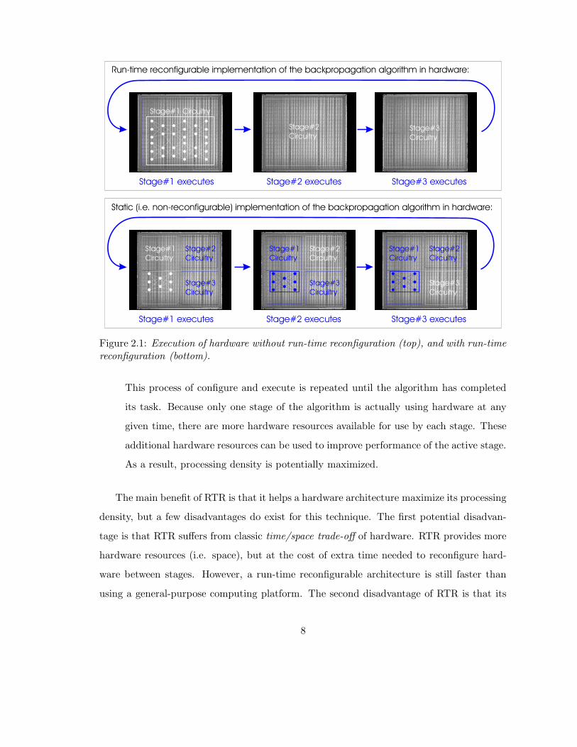
Stage#1 Circuitry
Stage#2
CircuitryStage#3
Circuitry
Run-time reconfigurable implementation of the backpropagation algorithm in hardware:
Stage#2 executesStage#1 executes Stage#3 executes
Stage#2
Circuitry
Stage#3
Circuitry
Stage#1
Circuitry
Stage#2
Circuitry
Stage#3
Circuitry
Stage#1
Circuitry
Static (i.e. non-reconfigurable) implementation of the backpropagation algorithm in hardware:
Stage#2 executesStage#1 executes Stage#3 executes
Stage#2
Circuitry
Stage#3
Circuitry
Stage#1
Circuitry
Figure 2.1: Execution of hardware without run-time reconfiguration (top), and with run-timereconfiguration (bottom).
This process of configure and execute is repeated until the algorithm has completed
its task. Because only one stage of the algorithm is actually using hardware at any
given time, there are more hardware resources available for use by each stage. These
additional hardware resources can be used to improve performance of the active stage.
As a result, processing density is potentially maximized.
The main benefit of RTR is that it helps a hardware architecture maximize its processing
density, but a few disadvantages do exist for this technique. The first potential disadvan-
tage is that RTR suffers from classic time/space trade-off of hardware. RTR provides more
hardware resources (i.e. space), but at the cost of extra time needed to reconfigure hard-
ware between stages. However, a run-time reconfigurable architecture is still faster than
using a general-purpose computing platform. The second disadvantage of RTR is that its
8

applicability is only feasible for algorithms that can be broken down into many stages. In
fact, the performance advantage of using a reconfigurable computing approach, whether it
be static (i.e. non-RTR) or run-time reconfigurable in nature, is the topic of focus in the
next section.
2.2.2 Performance Advantage of a Reconfigurable Computing Approach
How does one initially determine the performance advantage of using a reconfigurable com-
puting approach for a given algorithm? How does one justify if such an architecture should
be static (i.e. non-RTR) or run-time reconfigurable in nature? This section will review
these very issues.
Amdahl’s law [2] can act as a tool to help justify a hardware/software co-design. What
Amdahl’s law does is show the degree of software acceleration2 that can be achieved by a
certain algorithm. More formally, Amdahl’s law is stated as follows:
S(n) =S(1)
(1 − f) + fn
(2.1)
, where
S(n) = effective speedup by executing fraction f in hardware
f = fraction of algorithm that is parallelizable
n = number of processing elements (PEs) used
Equation 2.1 is best explained by considering a given algorithm which is initially im-
plemented entirely in software. Only a fraction f of this program is parallelizable, while
the remainder (1 − f) is purely sequential. Amdahl’s law makes an optimistic assumption
that the parallelizable part has a linear speedup. That is, with n processors, it will take
1nth the execution time needed on one processor. Hence, S(n) is the effective speedup with
2According to Edwards [31], this refers to the act of implementing computationally-intensive parts of analgorithm in hardware, while the remainder of the algorithm is implemented in software. Such an act isperformed to help satisfy timing constraints or reduce the overall execution of an algorithm.
9

n processors. It’s important to first conduct software profiling to identify the main bot-
tleneck in the software-only implementation of the algorithm. Only then can an engineer
estimate the speedup that can be achieved in the fraction of the algorithm (f) associated
with the bottleneck, which is representative of the typical speedup that can be achieved by
the system as a whole.
A hardware / software co-design is justified for algorithms which exhibit a large effective
speedup. Edwards [31] shows that the same is true in reconfigurable platforms (i.e. FPGA
co-processors). The key to success lies in the amount of hardware optimization, in terms
of the implementation of pipelining techniques and exploitation of parallelism, that can be
applied to a design. For example, backpropagation algorithm for ANNs is inherently mas-
sively parallel (i.e. f → 1). Therefore, Amdahl’s Law theoretically justifies a reconfigurable
approach for backprop-based ANNs by inspection.
Once Amdahl’s law has revealed that a reconfigurable computing approach is suitable
for a given algorithm, the next step is to justify whether this architecture should be either
run-time reconfigurable, or static (i.e. non-RTR) in nature.
Wirthlin’s functional density [51] metric can be used as a means of justifying the use
of RTR for a given algorithm. The primary condition which motivates / justifies
the use of RTR is the presence of idle or underutilized hardware. This metric is
based on the traditional way of quantifying the cost-performance of any hardware design,
as shown in Equation 2.2. For RTR designs, functional density is used to quantify the
trade-off between RTR performance and the added cost of configuration time, as shown
in Equation 2.3. For static (i.e. non-RTR) designs, configuration time is non-existent
when calculating functional density, as shown in Equation 2.4, since all stages of the given
algorithm are mapped into a single circuit. Justification of RTR is carried out by comparing
the functional density of run-time reconfigurable approach to its static equivalent for a given
algorithm. Note that RTR is only justified if it provides more functional density compared
10
to its static alternative, as shown in Equation 2.5.
FunctionalDensity(D) =Performance
Cost=
1/(ExecutionT ime)
(CircuitArea)(2.2)
DRTR =1
ARTR × (TE + TC)(2.3)
, where
DRTR = Functional Density of a run-time reconfigurable circuit
ARTR = Circuit area of configured stage used at any one time
TE = Total execution time of one complete iteration of algorithm
TC = Total configuration time of one complete iteration of algorithm
DS =1
AS × TE(2.4)
, where
DS = Functional Density of a static (i.e. non-RTR) circuit
AS = Total circuit area of static (i.e. non-RTR) architecture
DRTR > DS (2.5)
Wirthlin[51] showed that by using RTR, Eldredge’s RRANN architecture [15] for back-
propagation algorithm provided up to four times more functional density than that of its
static counterpart. However, the significant configuration overhead required by RRANN
would only allow RTR to be justified for ANN applications of at least 139 neurons.
11
2.2.3 Traditional Design Methodology for Reconfigurable Computing
A traditional hw/sw co-design methodology exists, which is most commonly used in embed-
ded systems design [32]. This same methodology can be applied to reconfigurable computing
designs, whose simplified design flow is shown in Figure 2.2.
At the System Definition Phase, the design functionality is specified and immediately
partitioned into hardware and software components. Hence, two paths of implementation
and verification are pursued in parallel: one for hardware; one for software. Hardware
design typically begins first, and is driven from HDL (Hardware Description Language) code.
Software capabilities are limited by the hardware architecture being designed. Therefore,
software design flow usually lags behind hardware design flow, and eventually waits for the
hardware before testing is complete. Once component testing for the two design flows has
been completed, the components are integrated together for system testing and validation.
Although this mature hw/sw co-design methodology can easily be applied to reconfig-
urable computing, the methodology does present some pitfalls:
System Design and Partitioning System Definition Phase is the only chance where de-
sign exploration is possible. Here, the fundamental design decisions which shape the
system architecture are often based on limited information gained from experimenta-
tion with an initial model (e.g. system modelling via general-purpose programming
language, or GPL). In addition, partitioning decisions are also done up front with
little means of knowing what implications will result. The problem is that there is no
easy way to revisit partitioning decisions. For example, once the hardware partition
of the model has been changed into a HDL/RTL (register transfer language) repre-
sentation, many design characteristics are effectively frozen, and cannot be changed
without significant effort. That is, in order to change significant design characteristics,
an new translation from model to HDL/RTL is required. This process is so costly in
terms of time / resources invested that, in most cases, the change is not feasible.
Hardware/Software Convergence The fact that two separate design flows exist in tra-
12
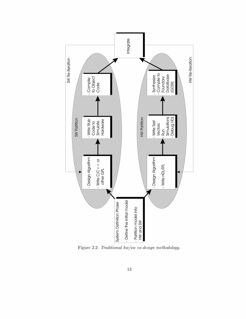
Syst
em
De
finiti
on P
ha
se
- D
efin
e the
initi
al m
od
el
- Pa
rtiti
on m
od
el i
nto
HW
and
SW
- D
esi
gn A
lgo
rithm
- W
rite
C/C
++
or
oth
er G
PL
- W
rite
Stu
b
Co
de
to
Sim
ula
te
Ha
rdw
are
- C
om
pile
to O
bje
ct
Co
de
Inte
gra
te
- D
esi
gn A
lgo
rithm
- W
rite
HD
L/RTL
- W
rite
Te
st
Ve
cto
rs
- Run
Sim
ula
tions
- D
eb
ug
HD
L
- Sy
nth
esi
ze
- C
om
pile
to
Found
ary
Da
tatb
ase
(GD
SII)
SW P
artiti
on
HW
Pa
rtiti
on
SW R
e-ite
ratio
n
HW
Re
-ite
ratio
n
Figure 2.2: Traditional hw/sw co-design methodology.
13
ditional hw/sw co-design results in a lack of convergence in the languages and design
methodologies used within each. As a result, hw/sw partitions are not easily inopera-
ble with one another, and two separate methodologies for one design can be complex
to manage.
System Verification Functional verification of the entire system is problematic. This
is due to the fact that verification strategies are dependent on partition type, be it
hardware or software. Here, hardware and software are verified independently, with
no way of knowing if system-level functionality has been achieved until Integration
stage.
System Implementation In traditional hw/sw co-design, there is discontinuity from sys-
tem definition (i.e. initial model) to hardware implementation. The original descrip-
tion used for algorithmic exploration (i.e. model) must be redesigned in RTL/HDL
before any hardware can be developed. Unfortunately, design problems can only be
realized at the end of the design flow integration.
Addressing these challenges is an ongoing research goal for the field of hw/sw co-design,
but are part of a working methodology for reconfigurable systems nonetheless. In summary,
this section has given an overview of a traditional hw/sw co-design methodology, which can
be used in the design and implementation of reconfigurable computing applications.
2.3 Field-Programmable Gate Array (FPGA) Overview
FPGAs are a form of programmable logic, which offer flexibility in design like software,
but with performance speeds closer to Application Specific Integrated Circuits (ASICs).
With the ability to be reconfigured an endless amount of times after it has already been
manufactured, FPGAs have traditionally been used as a prototyping tool for hardware
designers. However, as growing die capacities of FPGAs have increased over the years, so
has their use in reconfigurable computing applications too.
14
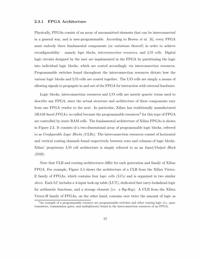
2.3.1 FPGA Architecture
Physically, FPGAs consist of an array of uncommitted elements that can be interconnected
in a general way, and is user-programmable. According to Brown et al. [6], every FPGA
must embody three fundamental components (or variations thereof) in order to achieve
reconfigurability – namely logic blocks, interconnection resources, and I/O cells. Digital
logic circuits designed by the user are implemented in the FPGA by partitioning the logic
into individual logic blocks, which are routed accordingly via interconnection resources.
Programmable switches found throughout the interconnection resources dictate how the
various logic blocks and I/O cells are routed together. The I/O cells are simply a means of
allowing signals to propagate in and out of the FPGA for interaction with external hardware.
Logic blocks, interconnection resources and I/O cells are merely generic terms used to
describe any FPGA, since the actual structure and architecture of these components vary
from one FPGA vendor to the next. In particular, Xilinx has traditionally manufactured
SRAM-based FPGAs; so-called because the programmable resources3 for this type of FPGA
are controlled by static RAM cells. The fundamental architecture of Xilinx FPGAs is shown
in Figure 2.3. It consists of a two-dimensional array of programmable logic blocks, referred
to as Configurable Logic Blocks (CLBs). The interconnection resources consist of horizontal
and vertical routing channels found respectively between rows and columns of logic blocks.
Xilinx’ proprietary I/O cell architecture is simply referred to as an Input/Output Block
(IOB).
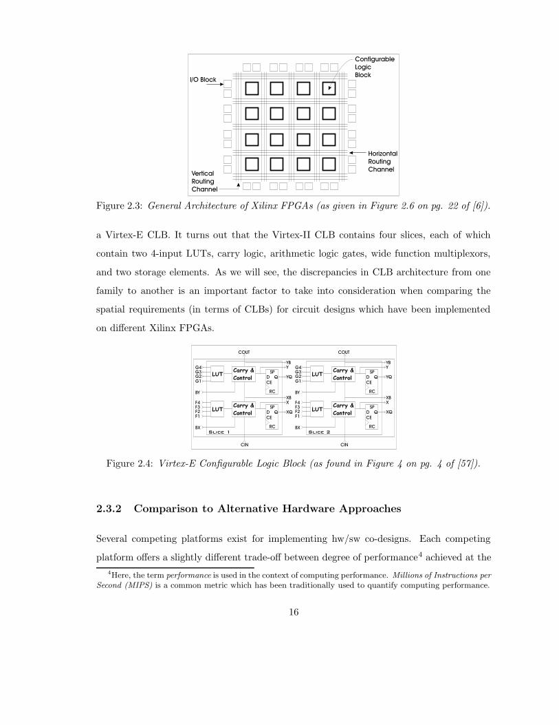
Note that CLB and routing architectures differ for each generation and family of Xilinx
FPGA. For example, Figure 2.4 shows the architecture of a CLB from the Xilinx Virtex-
E family of FPGAs, which contains four logic cells (LCs) and is organized in two similar
slices. Each LC includes a 4-input look-up table (LUT), dedicated fast carry-lookahead logic
for arithmetic functions, and a storage element (i.e. a flip-flop). A CLB from the Xilinx
Virtex-II family of FPGAs, on the other hand, contains over twice the amount of logic as
3An example of a programmable resource are programmable switches and other routing logic (i.e. pass-transistors, transmission gates, and multiplexors) found in the interconnection resources of an FPGA.
15
I/O Block
Vertical
Routing
Channel
Horizontal
Routing
Channel
Configurable
Logic
Block
Figure 2.3: General Architecture of Xilinx FPGAs (as given in Figure 2.6 on pg. 22 of [6]).
a Virtex-E CLB. It turns out that the Virtex-II CLB contains four slices, each of which
contain two 4-input LUTs, carry logic, arithmetic logic gates, wide function multiplexors,
and two storage elements. As we will see, the discrepancies in CLB architecture from one
family to another is an important factor to take into consideration when comparing the
spatial requirements (in terms of CLBs) for circuit designs which have been implemented
on different Xilinx FPGAs.
LUTCarry &
ControlSP
D Q
CE
RC
G4
G3
G2
G1
BY
COUT
YB
Y
YQ
LUTCarry &
ControlSP
D Q
CE
RC
F4
F3
F2
F1
BX
XB
X
XQ
CIN
Slice 1
LUTCarry &
ControlSP
D Q
CE
RC
G4
G3
G2
G1
BY
COUT
YB
Y
YQ
LUTCarry &
ControlSP
D Q
CE
RC
F4
F3
F2
F1
BX
XB
X
XQ
CIN
Slice 2
Figure 2.4: Virtex-E Configurable Logic Block (as found in Figure 4 on pg. 4 of [57]).
2.3.2 Comparison to Alternative Hardware Approaches
Several competing platforms exist for implementing hw/sw co-designs. Each competing
platform offers a slightly different trade-off between degree of performance4 achieved at the
4Here, the term performance is used in the context of computing performance. Millions of Instructions perSecond (MIPS) is a common metric which has been traditionally used to quantify computing performance.
16
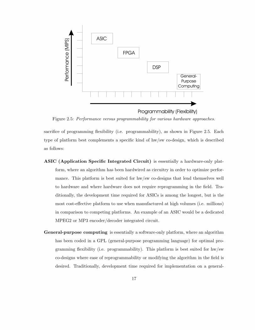
ASIC
FPGA
DSP
General-
Purpose
Computing
Programmability (Flexibility)
Perfo
rma
nc
e (M
IPS)
Figure 2.5: Performance versus programmability for various hardware approaches.
sacrifice of programming flexibility (i.e. programmability), as shown in Figure 2.5. Each
type of platform best complements a specific kind of hw/sw co-design, which is described
as follows:
ASIC (Application Specific Integrated Circuit) is essentially a hardware-only plat-
form, where an algorithm has been hardwired as circuitry in order to optimize perfor-
mance. This platform is best suited for hw/sw co-designs that lend themselves well
to hardware and where hardware does not require reprogramming in the field. Tra-
ditionally, the development time required for ASICs is among the longest, but is the
most cost-effective platform to use when manufactured at high volumes (i.e. millions)
in comparison to competing platforms. An example of an ASIC would be a dedicated
MPEG2 or MP3 encoder/decoder integrated circuit.
General-purpose computing is essentially a software-only platform, where an algorithm
has been coded in a GPL (general-purpose programming language) for optimal pro-
gramming flexibility (i.e. programmability). This platform is best suited for hw/sw
co-designs where ease of reprogrammability or modifying the algorithm in the field is
desired. Traditionally, development time required for implementation on a general-
17

purpose computing medium, such as microprocessor unit, is minimal compared to
competing technologies.
FPGA is a platform that provides performance similar to ASIC whilst maintaining pro-
gramming flexibility (i.e. programmability) similar to general-purpose computing.
This platform is best suited for hw/sw co-designs which require optimal trade-off be-
tween performance and programming flexibility, especially algorithms suitable enough
to utilize RTR.
DSP (Digital Signal Processing) is a niche platform, which offers dedicated hardware
resources commonly used to accelerate DSP algorithms. For example, this platform
could easily be reprogrammed to implement such algorithms as MPEG2 or MP3 de-
coder/encoder programs in GPL (i.e. general-purpose programming language). This
platform is best suited for quickly prototyping DSP algorithms, but has been tradi-
tionally shown to lack in performance compared to ASIC and FPGA (where RTR
utilized) platforms [44].
2.4 Artificial Neural Network (ANN) Overview
2.4.1 Introduction
Artificial neural networks (ANNs) are a form of artificial intelligence, which have been
modelled after, and inspired by the processes of the human brain. Structurally, ANNs
consist of massively parallel, highly interconnected processing elements. In theory, each
processing element, or neuron, is far too simplistic to learn anything meaningful on its own.
Significant learning capacity, and hence, processing power only comes from the culmina-
tion of many neurons inside a neural network. The learning potential of ANNs has been
demonstrated in different areas of application, such as pattern recognition [48], function
approximation/prediction [15], and robot control [42].
18
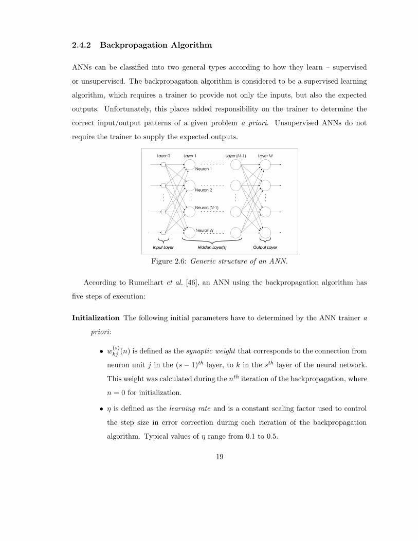
2.4.2 Backpropagation Algorithm
ANNs can be classified into two general types according to how they learn – supervised
or unsupervised. The backpropagation algorithm is considered to be a supervised learning
algorithm, which requires a trainer to provide not only the inputs, but also the expected
outputs. Unfortunately, this places added responsibility on the trainer to determine the
correct input/output patterns of a given problem a priori. Unsupervised ANNs do not
require the trainer to supply the expected outputs.
Input Layer Hidden Layer(s) Output Layer
Layer 0 Layer 1 Layer ( -1)M Layer M
Neuron 1
Neuron 2
Neuron ( -1)N
Neuron N
Figure 2.6: Generic structure of an ANN.
According to Rumelhart et al. [46], an ANN using the backpropagation algorithm has
five steps of execution:
Initialization The following initial parameters have to determined by the ANN trainer a
priori :
• w(s)kj (n) is defined as the synaptic weight that corresponds to the connection from
neuron unit j in the (s − 1)th layer, to k in the sth layer of the neural network.
This weight was calculated during the nth iteration of the backpropagation, where
n = 0 for initialization.
• η is defined as the learning rate and is a constant scaling factor used to control
the step size in error correction during each iteration of the backpropagation
algorithm. Typical values of η range from 0.1 to 0.5.
19
• θ(s)k is defined as the bias of a neuron, which is similar to synaptic weight in that
it corresponds to a connection to neuron unit k in the sth layer of the ANN,
but is NOT connected to any neuron unit j in the (s − 1)th layer. Statistically,
biases can be thought of as noise, which better randomizes initial conditions, and
increases the chances of convergence for an ANN. Typical values of θ(s)k are the
same as those used for synaptic weights(
w(s)kj (n)
)
in a given application.
Presentation of Training Examples Using the training data available, present the ANN
with one or more epoch. An epoch, as defined by Haykin [20], is one complete presen-
tation of the entire training set during the learning process. For each training example
in the set, perform forward followed by backward computations consecutively.
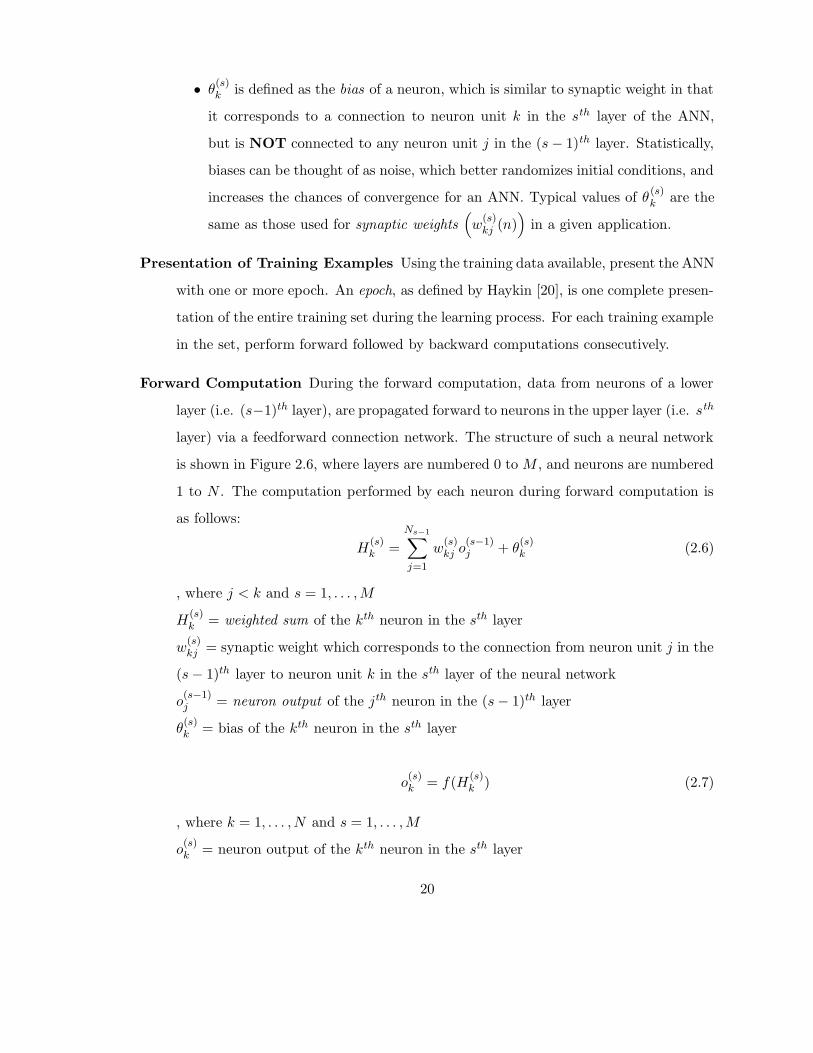
Forward Computation During the forward computation, data from neurons of a lower
layer (i.e. (s−1)th layer), are propagated forward to neurons in the upper layer (i.e. sth
layer) via a feedforward connection network. The structure of such a neural network
is shown in Figure 2.6, where layers are numbered 0 to M , and neurons are numbered
1 to N . The computation performed by each neuron during forward computation is
as follows:
H(s)k =
Ns−1∑
j=1
w(s)kj o
(s−1)j + θ
(s)k (2.6)
, where j < k and s = 1, . . . ,M
H(s)k = weighted sum of the kth neuron in the sth layer
w(s)kj = synaptic weight which corresponds to the connection from neuron unit j in the
(s − 1)th layer to neuron unit k in the sth layer of the neural network
o(s−1)j = neuron output of the jth neuron in the (s − 1)th layer
θ(s)k = bias of the kth neuron in the sth layer
o(s)k = f(H
(s)k ) (2.7)
, where k = 1, . . . , N and s = 1, . . . ,M
o(s)k = neuron output of the kth neuron in the sth layer
20
f(H(s)k ) = activation function computed on the weighted sum H
(s)k
Note that some sort of sigmoid function is often used as the nonlinear activation
function, such as the logsig function shown in the following:
f(x)logsig =1
1 + exp(−x)(2.8)
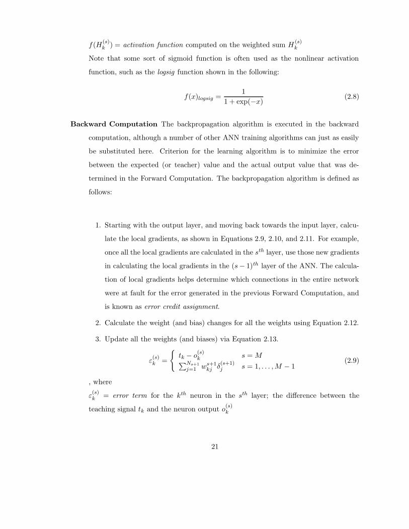
Backward Computation The backpropagation algorithm is executed in the backward
computation, although a number of other ANN training algorithms can just as easily
be substituted here. Criterion for the learning algorithm is to minimize the error
between the expected (or teacher) value and the actual output value that was de-
termined in the Forward Computation. The backpropagation algorithm is defined as
follows:
1. Starting with the output layer, and moving back towards the input layer, calcu-
late the local gradients, as shown in Equations 2.9, 2.10, and 2.11. For example,
once all the local gradients are calculated in the sth layer, use those new gradients
in calculating the local gradients in the (s− 1)th layer of the ANN. The calcula-
tion of local gradients helps determine which connections in the entire network
were at fault for the error generated in the previous Forward Computation, and
is known as error credit assignment.
2. Calculate the weight (and bias) changes for all the weights using Equation 2.12.
3. Update all the weights (and biases) via Equation 2.13.
ε(s)k =
{
tk − o(s)k s = M
∑Ns+1
j=1 ws+1kj δ
(s+1)j s = 1, . . . ,M − 1
(2.9)
, where
ε(s)k = error term for the kth neuron in the sth layer; the difference between the
teaching signal tk and the neuron output o(s)k
21
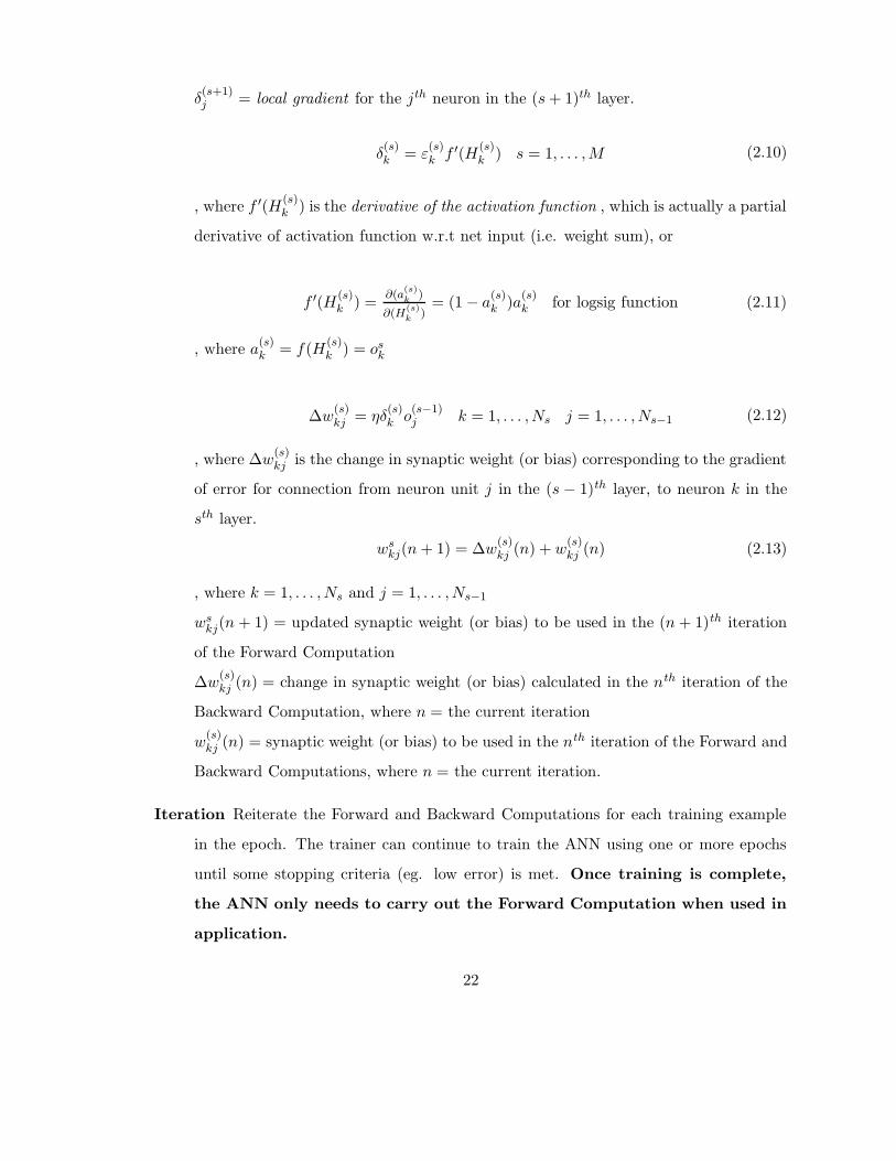
δ(s+1)j = local gradient for the jth neuron in the (s + 1)th layer.
δ(s)k = ε
(s)k f ′(H
(s)k ) s = 1, . . . ,M (2.10)
, where f ′(H(s)k ) is the derivative of the activation function , which is actually a partial
derivative of activation function w.r.t net input (i.e. weight sum), or
f ′(H(s)k ) =
∂(a(s)k
)
∂(H(s)k
)= (1 − a
(s)k )a
(s)k for logsig function (2.11)
, where a(s)k = f(H
(s)k ) = os
k
∆w(s)kj = ηδ
(s)k o
(s−1)j k = 1, . . . , Ns j = 1, . . . , Ns−1 (2.12)
, where ∆w(s)kj is the change in synaptic weight (or bias) corresponding to the gradient
of error for connection from neuron unit j in the (s − 1)th layer, to neuron k in the
sth layer.
wskj(n + 1) = ∆w
(s)kj (n) + w
(s)kj (n) (2.13)
, where k = 1, . . . , Ns and j = 1, . . . , Ns−1
wskj(n + 1) = updated synaptic weight (or bias) to be used in the (n + 1)th iteration
of the Forward Computation
∆w(s)kj (n) = change in synaptic weight (or bias) calculated in the nth iteration of the
Backward Computation, where n = the current iteration
w(s)kj (n) = synaptic weight (or bias) to be used in the nth iteration of the Forward and
Backward Computations, where n = the current iteration.
Iteration Reiterate the Forward and Backward Computations for each training example
in the epoch. The trainer can continue to train the ANN using one or more epochs
until some stopping criteria (eg. low error) is met. Once training is complete,
the ANN only needs to carry out the Forward Computation when used in
application.
22
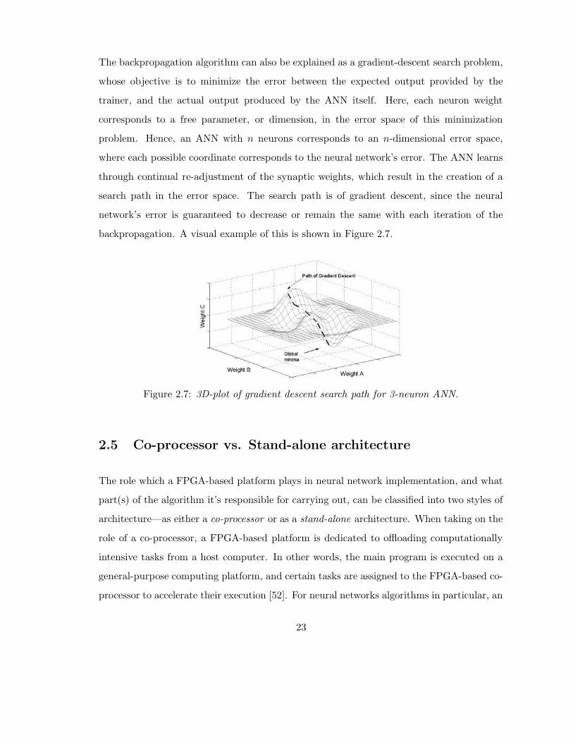
The backpropagation algorithm can also be explained as a gradient-descent search problem,
whose objective is to minimize the error between the expected output provided by the
trainer, and the actual output produced by the ANN itself. Here, each neuron weight
corresponds to a free parameter, or dimension, in the error space of this minimization
problem. Hence, an ANN with n neurons corresponds to an n-dimensional error space,
where each possible coordinate corresponds to the neural network’s error. The ANN learns
through continual re-adjustment of the synaptic weights, which result in the creation of a
search path in the error space. The search path is of gradient descent, since the neural
network’s error is guaranteed to decrease or remain the same with each iteration of the
backpropagation. A visual example of this is shown in Figure 2.7.
Figure 2.7: 3D-plot of gradient descent search path for 3-neuron ANN.
2.5 Co-processor vs. Stand-alone architecture
The role which a FPGA-based platform plays in neural network implementation, and what
part(s) of the algorithm it’s responsible for carrying out, can be classified into two styles of
architecture—as either a co-processor or as a stand-alone architecture. When taking on the
role of a co-processor, a FPGA-based platform is dedicated to offloading computationally
intensive tasks from a host computer. In other words, the main program is executed on a
general-purpose computing platform, and certain tasks are assigned to the FPGA-based co-
processor to accelerate their execution [52]. For neural networks algorithms in particular, an
23

FPGA-based co-processor has been traditionally used to accelerate the processing elements
(eg. neurons) [15].
On the other hand, when a FPGA-based platform takes on the role of a stand-alone
architecture, it becomes self-contained and does not depend on any other devices to function.
In relation to a co-processor, a stand-alone architecture does not depend on a host computer,
and is responsible for carrying out all the tasks of a given algorithm.
There are design tradeoffs associated with each style of architecture. In the case of the
stand-alone architecture, it is often more embedded and compact than a system containing
a general-purpose computing platform (i.e. host computer) and FPGA-based co-processor.
However, a FPGA-based co-processor allows for a hardware/software co-design, whereas a
stand-alone FPGA platform is restricted to a hardware-only design. Although hardware is
faster than software, an algorithm mapped entirely in hardware (i.e. on an FPGA) does
not imply that it will outperform an equivalent hardware/software co-design5.
Most often, the length of time required for software development is much less than that
of hardware development, depending on the algorithm being implemented. Therefore, ad-
ditional development overhead commonly associated with a hardware-only approach, com-
pared to hardware/software co-design may not be justifiable if the difference in performance
gain is minimal. This may have been the very reason why all seven FPGA-based ANN im-
plementations surveyed in the next chapter utilized co-processors, with the exception of
Perez-Uribe’s mobile robot application.
Before an algorithm can be ’mapped’ onto an FPGA architecture, an engineer must
first break down the algorithm into a number of finite steps. The next step is the process
of hardware/software co-design, where an engineer has to determine what subset of steps
he/she wishes to implement in hardware, and what remaining steps need to be implemented
in software. The proper execution of those steps the engineer has chosen to implement in
digital hardware can then be ’mapped’ using the traditional control unit/datapath method-
5This is especially the case when the implemented algorithm is largely sequential in nature. For moreinformation, please refer to the discussion on Amdahl’s Law, in section 2.2.2
24

ology of design [29]. The control unit acts as a finite state machine which is responsible for
ensuring the finite steps of the algorithm occur in the proper sequence, whereas the data-
path consists of various processing elements (eg. ALU). The subset of processing elements
chosen to operate on data (i.e. the path though which data flows) at any given time, and
order in which they’re used, is dictated by the control unit.
The various sub-components which make up the generic architecture of an FPGA co-
processor, as shown in Figure 2.8, are described as follows:
Host Computer
Main
Program
Memory
(RAM)
Processing Elements
(e.g. neurons)
Control
Unit
Co-processor
Interconnect
(i.e. 'glue logic')
Figure 2.8: Generic co-processor architecture for an FPGA-based platform.
Host Computer. A general-purpose computing platform is used to house the main pro-
gram which acts as the master controller of the entire system [50]. From the control
unit’s point of view, the main program is seen as a software driver, since it’s the main
program that actually ’drives’ the FPGA-based co-processor’s control unit. The main
program is often responsible for, but not limited to, the following tasks:
25
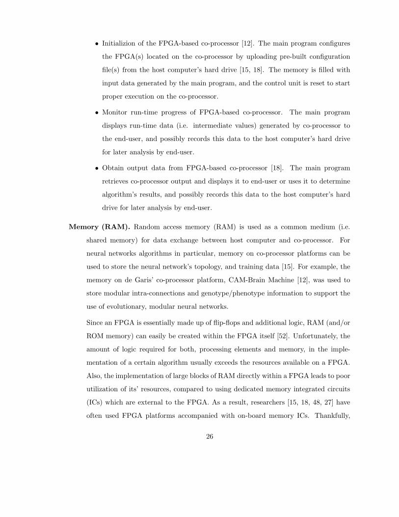
• Initializion of the FPGA-based co-processor [12]. The main program configures
the FPGA(s) located on the co-processor by uploading pre-built configuration
file(s) from the host computer’s hard drive [15, 18]. The memory is filled with
input data generated by the main program, and the control unit is reset to start
proper execution on the co-processor.
• Monitor run-time progress of FPGA-based co-processor. The main program
displays run-time data (i.e. intermediate values) generated by co-processor to
the end-user, and possibly records this data to the host computer’s hard drive
for later analysis by end-user.
• Obtain output data from FPGA-based co-processor [18]. The main program
retrieves co-processor output and displays it to end-user or uses it to determine
algorithm’s results, and possibly records this data to the host computer’s hard
drive for later analysis by end-user.
Memory (RAM). Random access memory (RAM) is used as a common medium (i.e.
shared memory) for data exchange between host computer and co-processor. For
neural networks algorithms in particular, memory on co-processor platforms can be
used to store the neural network’s topology, and training data [15]. For example, the
memory on de Garis’ co-processor platform, CAM-Brain Machine [12], was used to
store modular intra-connections and genotype/phenotype information to support the
use of evolutionary, modular neural networks.
Since an FPGA is essentially made up of flip-flops and additional logic, RAM (and/or
ROM memory) can easily be created within the FPGA itself [52]. Unfortunately, the
amount of logic required for both, processing elements and memory, in the imple-
mentation of a certain algorithm usually exceeds the resources available on a FPGA.
Also, the implementation of large blocks of RAM directly within a FPGA leads to poor
utilization of its’ resources, compared to using dedicated memory integrated circuits
(ICs) which are external to the FPGA. As a result, researchers [15, 18, 48, 27] have
often used FPGA platforms accompanied with on-board memory ICs. Thankfully,
26
newer FPGA architectures have dedicated memory blocks embedded within them.
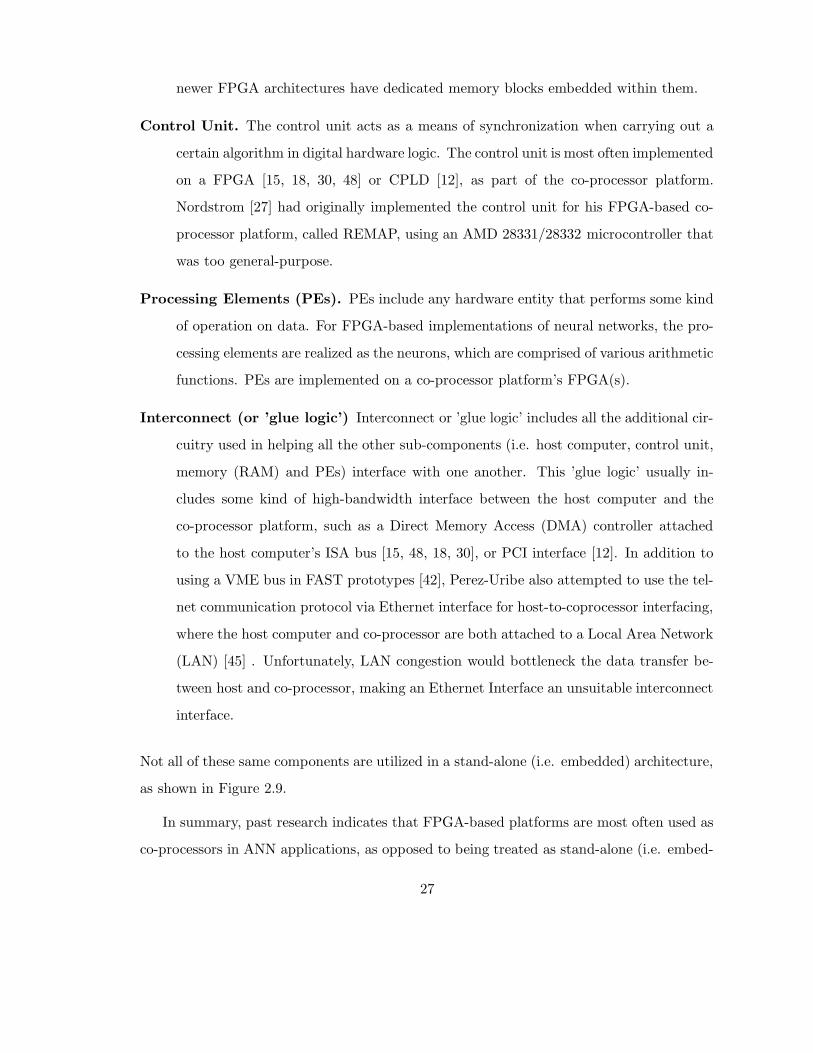
Control Unit. The control unit acts as a means of synchronization when carrying out a
certain algorithm in digital hardware logic. The control unit is most often implemented
on a FPGA [15, 18, 30, 48] or CPLD [12], as part of the co-processor platform.
Nordstrom [27] had originally implemented the control unit for his FPGA-based co-
processor platform, called REMAP, using an AMD 28331/28332 microcontroller that
was too general-purpose.
Processing Elements (PEs). PEs include any hardware entity that performs some kind
of operation on data. For FPGA-based implementations of neural networks, the pro-
cessing elements are realized as the neurons, which are comprised of various arithmetic
functions. PEs are implemented on a co-processor platform’s FPGA(s).
Interconnect (or ’glue logic’) Interconnect or ’glue logic’ includes all the additional cir-
cuitry used in helping all the other sub-components (i.e. host computer, control unit,
memory (RAM) and PEs) interface with one another. This ’glue logic’ usually in-
cludes some kind of high-bandwidth interface between the host computer and the
co-processor platform, such as a Direct Memory Access (DMA) controller attached
to the host computer’s ISA bus [15, 48, 18, 30], or PCI interface [12]. In addition to
using a VME bus in FAST prototypes [42], Perez-Uribe also attempted to use the tel-
net communication protocol via Ethernet interface for host-to-coprocessor interfacing,
where the host computer and co-processor are both attached to a Local Area Network
(LAN) [45] . Unfortunately, LAN congestion would bottleneck the data transfer be-
tween host and co-processor, making an Ethernet Interface an unsuitable interconnect
interface.
Not all of these same components are utilized in a stand-alone (i.e. embedded) architecture,
as shown in Figure 2.9.
In summary, past research indicates that FPGA-based platforms are most often used as
co-processors in ANN applications, as opposed to being treated as stand-alone (i.e. embed-
27
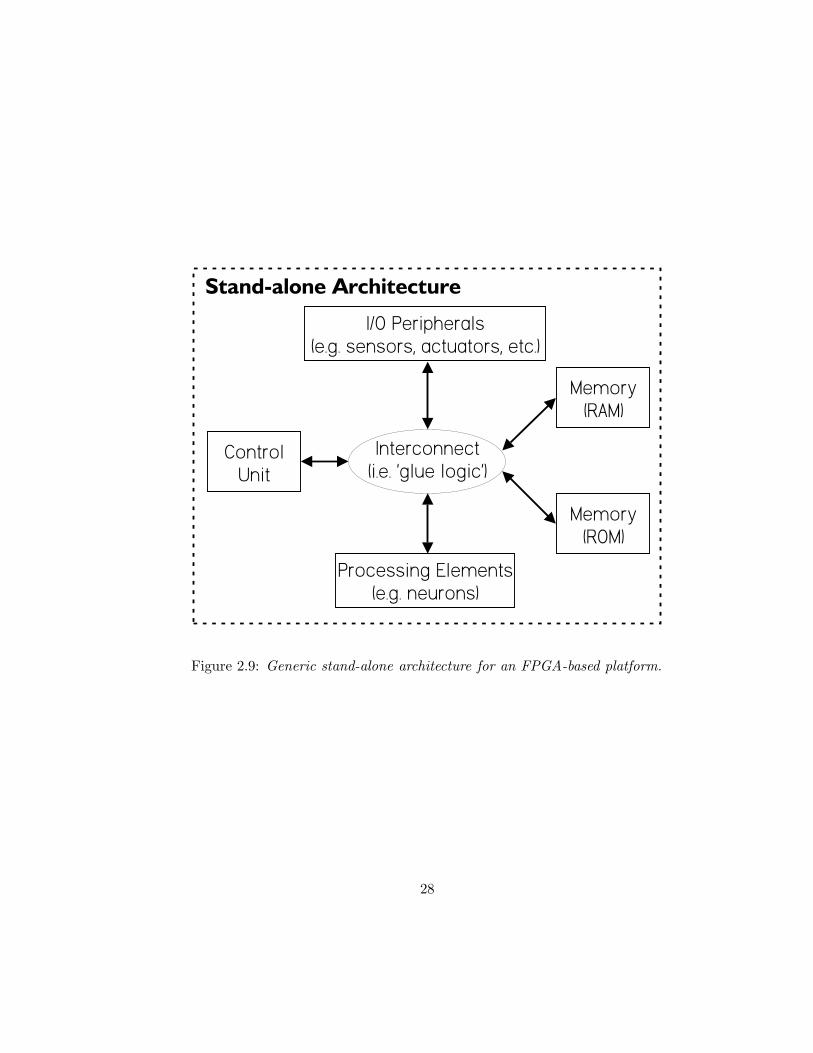
Stand-alone Architecture
Memory
(RAM)
Processing Elements
(e.g. neurons)
Control
Unit
Interconnect
(i.e. 'glue logic')
I/O Peripherals
(e.g. sensors, actuators, etc.)
Memory
(ROM)
Figure 2.9: Generic stand-alone architecture for an FPGA-based platform.
28
ded) architectures. This may be due to the fact that co-processors are traditionally more
flexible to design / implement with compared to stand-alone (i.e. embedded) architectures.
2.6 Conclusion
In summary, this chapter has clearly reviewed the different fields of study which cover all
aspects of reconfigurable architectures for ANNs, including:
Technique for Accelerating Performance - Reconfigurable computing can help im-
prove the processing density of a given application, which can only be maximized
when RTR is used. This chapter has shown how Amdahl’s law and Wirthlin’s func-
tional density metric can be used to justify a reconfigurable computing approach and
RTR respectively, for a given application. This chapter has also shown how a tra-
ditional hw/sw design methodology can be applied to the creation of reconfigurable
computing applications.
Physical Medium Used - FPGAs are the means by which reconfigurable computing is
achieved. Hence, this chapter gave an in-depth look at FPGA technology, and ex-
plained how it is the medium best suited for reconfigurable computing compared to
alternative h/w approaches.
Area of Application - ANNs were identified as an application area which can reap the
benefits of reconfigurable computing. In particular, this chapter focused on the expla-
nation of the backpropagation algorithm, since the popularity and slow convergence
rates of this type of ANN make it a good candidate for reconfigurable computing.
Several generic system architectures commonly used to build reconfigurable architectures
for ANNs were reviewed, the most popular type being the co-processor. The next chapter
will survey several specific FPGA-based ANN architectures created by past researchers in
the field.
29
Chapter 3
Survey of Neural Network
Implementations on FPGAs
3.1 Introduction
There has been a rich history of attempts at implementing ASIC-based approaches for
neural networks - traditionally referred to as neuroprocessors [50] or neurochips. FPGA-
based implementations, on the other hand, are still a fairly new approach which has only
been in effect since the early 1990s. Since the approach of this thesis is to use a reconfigurable
architecture for neural networks, this review is narrowed to FPGA implementations only.
Past attempts made at implementing neural network applications onto FPGAs will be
surveyed and classified based on the respective design decisions made in each case. Such
classification will provide a medium upon which the advantages / disadvantages of each
implementation can be discussed and clearly understood. Such discussion will not only
help identify some of the common problems that past researchers have been faced with in
this field (i.e. the design and implementation of FPGA-based ANNs), but will also identify
the problems that have yet to be fully addressed. A summary of each implementation’s
results will also be provided, whose past successes and failures were largely based on the
30

limitations of technologies / tools available at that time.
3.2 Classification of Neural Networks Implementations on
FPGAs
FPGA-based neural networks can be classified using the following features:
• Learning Algorithm Implemented
• Signal Representation
• Multiplier Reduction Schemes
3.2.1 Learning Algorithm Implemented
The type of neural network refers to the algorithm used for on-chip learning 1, and is de-
pendent upon its intended application. Backpropagation-based neural networks currently
stand out as the most popular type of neural network used to date ([42], [37], [17], [5]).
Eldredge [15] successfully implemented the backpropagation algorithm using a custom
platform he built out of Xilinx XC3090 FPGAs, called the Run-Time Reconfiguration Ar-
tificial Neural Network (RRANN). Eldredge proved that the RRANN architecture could
learn how to approximate centroids of fuzzy sets. Results showed that RRANN converged
on the training set, once 92% of the training data came within two quantization errors
(1/16) of the actual value, and that RRANN generalized well since 88% of approximations
calculated by RRANN (based on randomized inputs) came within two quantization values
[15]. Heavily influenced by the Eldredge’s RRANN architecture, Beuchat et al. [5] de-
veloped a FPGA platform, called RENCO–a REconfigurable Network COmputer. As it’s
1According to Perez [42], on-chip learning occurs when the learning algorithm is implemented in hardware,or in this case, on the FPGA. Offline learning occurs when learning (i.e. modification of neural weights)has already occurred on a general-purpose computing platform before the learned system is implemented inhardware.
31
name implies, RENCO contains four Altera FLEX 10K130 FPGAs that can be reconfigured
and monitored over any LAN (i.e. Internet or other) via an onboard 10Base-T interface.
RENCO’s intended application was hand-written character recognition.
Ferrucci and Martin [18, 30] built a custom platform, called Adaptive Connectionist
Model Emulator (ACME) which consists of multiple Xilinx XC4010 FPGAs. ACME was
successfully validated by implementing a 3-input, 3-hidden unit, 1-output network used
to learn the 2-input XOR problem [18]. Skrbek also used this problem to prove that his
own custom backpropagation-based FPGA platform worked [48]. Skrbek’s FPGA platform
[48], called the ECX card, could also implement Radial Basis Function (RBF) neural net-
works, and was validated using pattern recognition applications such as parity problem,
digit recognition, inside-outside test, and sonar signal recognition.
One challenge in implementing the backprop on FPGA is the sequential nature of pro-
cessing between layers (as shown in Equations 2.6 to 2.8). A major challenge is that pipelin-
ing of the algorithm on a whole cannot occur during training [15]. This problem arises due
to the weight update dependencies of backpropagation, and as a result, the utilization of
hardware resources dedicated to each of the neural network’s layers is wasted [5]. However,
it’s still possible to use fine-grain pipelining in each of the individual arithmetic functions
of the backpropagation algorithm, which could help increase both, data throughput and
global clock speeds [15].
There also exists various other reasons why researchers decide to use alternative neural
networks besides the backpropagation-based ones. Perez-Uribe’s research ([42]) was moti-
vated on the premise that neural networks used to adaptively control robots (i.e. neuro–
controllers) should learn from interaction or learn by example. Perez-Uribe found that
this kind of notion would be limited by the difficulty of determining a neural network’s
topology2, which he wanted to overcome using evolutionary3 neural networks.
2A neural network topology refers to the number of layers, the number of neurons in each layer, andinterconnection scheme used.
3’Evolutionary’ in the context of neural networks is defined as the systematic (i.e. autonomous) adaptationof a topology to the given task at hand.
32
As such he implements what he calls ontonogenic neural networks on a custom FPGA
platform, called Flexible Adaptable-Size Topology (FAST). FAST was used to implement
three different kinds of unsupervised, ontogenic neural networks—adaptive resonance theory
(ART), adaptive heuristic critic (AHC), and Dyna-SARSA.
The first implementation of FAST used an ART-based neural network. When applied to
a colour image segmentation problem, four FAST neurons successfully segmented a 294x353,
61-colour pixel image of Van Gogh’s Sunflowers painting into four colour classifications.
The second implementation of FAST used an AHC-based neural network [43]. In this
particular implementation, called FAST-AHC, eight neurons were used to control the in-
verted pendulum problem. The inverted pendulum problem is a classic example of an inher-
ently unstable system, used to test new approaches to learning control (Perez-Uribe, [42]).
The FAST-AHC couldn’t generalize as well as the backpropagation algorithm, but can learn
faster and more efficiently. This is due to the fact that AHC’s learning technique can be
generalized as a form of localized learning [41], where only the active nodes in the neural
network are updated, as opposed to the backpropagation which performs global learning.
The third, and final, implementation of FAST used a Dyna-SARSA neural network [42].
Dyna-SARSA is another type of reinforcement learning, was even less computationally
intensive compared to AHC, and well-suited for digital implementation. The FAST Dyna-
SARSA platform was integrated onto a stand-alone mobile robot, and used as a neurocon-
troller to demonstrate a navigation-learning task. The FAST Dyna-SARSA neurocontroller
was successful in helping the mobile robot avoid obstacles, which adapted to slight changes
in the position of obstacles.
The FAST architecture was the first of its kind to use unsupervised, ontogenic neural
networks, but admitted that the FAST architecture is somewhat limited, since it can only
handle toy problems which require dynamic categorization or online clustering.
Contrary to Perez-Uribe’s beliefs, de Garis et al [12, 11] implemented an evolutionary
neural network based on evolutionary techniques4, and still managed to achieve on-chip
4For a more in-depth discussion of evolutionary techniques, please refer to Yao’s [58] pioneering work in
33

learning. Largely influenced by MIT’s CAM project5, de Garis designed a FPGA-based
platform, called the CAM-Brain Machine (CBM), where a genetic algorithm (GA) is used
to evolve a cellular automata (CA) based neural network. Although CBM qualifies as hav-
ing on-chip learning, no learning algorithm was explicitly included into the CA. Instead,
localized learning indirectly occurs by first evolving the genetic algorithm’s phenotype chro-
mosome (i.e. in this case it initializes the configuration data of each cellular automata, which
dictates how the network will grow), followed by letting the topology of a neural network
module ’grow’, which is a functional characteristic of cellular automata.
CBM currently supports up to 75 million neurons, making it the worlds largest6 evolving
neural network to date, where thousands of neurons are evolved in a few seconds. The
CBM proved successful in function approximation/predictor applications, including a 3-bit
comparator, a timer, and a sinusoidal function. De Garis’ long-term goal is to use the CBM
to create extremely fast, large-scale modular 7 neural networks, which can be used in brain
building applications. For example, de Garis plans on using CBM as a neurocontroller in
the real-time control of a life-sized robot kitten called ”Robokitty”.
Support for modular neural networks on the CBM is somewhat limited, since the inter-
action of these modules or ’inter-modular’ connections have to be manually defined offline.
Nordstrom [40] also attempted to feature modular neural networks in a FPGA-based
platform he helped design, called REMAP (Real-time, Embedded, Modular, Adaptive,
Parallel processor). Nordstrom contemplated that reconfigurable computing could be used
as a suitable platform to easily support different types of modules (i.e. different neural
network algorithms). This kind of medium could be used in creating a heterogeneous
modular neural network, like the ’hierarchy of experts’ proposed by Jordan and Jacobs [36].
In 1992, Nordstrom made the following observations in regards to hardware support for
modular neural networks:
Evolutionary Neural Networks.5Margolus and Toffoli designed 8 versions of their Cellular Automata Machine (CAM) at MIT. The last
version developed in 1994, called CAM-8, could simulate over 10 million artificial neurons.6This has been confirmed by Guniess World Book of Records.7Please refer to the works of Auda and Kamel [4] for an in-depth survey of modular neural networks.
34

But when it comes to a number of cooperating ANN modules relatively few ex-
periments have been done, and there is no hardware around with the capacity to
do real-time simulation of multi-ANN systems big enough to be interesting [37].
With the possible exception of de Garis’ CAM-Brain Machine, much of Nordstrom’s obser-
vations about the field still remain valid today. Unfortunately, due to the limited FPGA
densities offered at the time of his research, Nordstrom was only able to implement single
module applications on REMAP. Ideally, Nordstrom wanted to support the use of modular
neural networks on REMAP, but was forced to leave this as a future research goal that was
never fulfilled ([40], pg. 11).
REMAP was a joint project of Lulea University of Technology, Chalmers University of
Technology, and Halmstad University, all of which are located in Sweden. As a result, many
researchers were involved with REMAP throughout it’s lifetime, during which a number of
prototypes were built. For example, Norstrom worked on designing and mapping neural
network algorithms onto the FPGAs of the first prototype, called REMAP-α, whereas
Taveniku and Linde [50] later concentrated their efforts on helping to develop a second
prototype, called REMAP-β.
The difference between the REMAP-α and REMAP-β are the size of FPGA densities
used in each. The REMAP-α used Xilinx XC3090 FPGAs for prototyping different neural
network algorithms, whereas the REMAP-β initially used Xilinx XC4005 FPGAs, but were
replaced with Xilinx XC4025. The REMAP-β was used as a neural network hardware
emulator and teaching tool, which could implement the following types of neural networks:
• Adaline and Madaline Networks
• Backpropagation algorithm
• Bidirectional Associative Memory Network
• Sparse Distributed Memory (SDM) Network [49, 38]
• Hopfield Associative Memory
35
• Counterpropagation Network
• Self-organizing Maps (SOM) [35]
• Adaptive Resonance Theory (ART)
In order to increase processing speed further, a third and final prototype called REMAP-γ
was built using an ASIC-based approach, the details of which are beyond the scope of this
thesis.
In summary, the type of neural network used in FPGA-based implementations is an
important feature used in classifying such architectures. The type of neural network applied
depends on the intended application used to solve the problem at hand. For each of the
seven FPGA-based neural network implementations surveyed, the intended application(s)
and type of neural network(s) used have been summarized and compared. Current trends in
the this field have shown that there have been very few attempts at implementing modular
neural networks on FPGA-based platforms. In the past, this can be attributed to the fact
that FPGA densities and speeds were inadequate for supporting modular neural networks.
However, FPGAs densities and speeds have now improved to the point where it’s far more
feasible to support modular neural networks, and attempts at doing so should be re-visited.
3.2.2 Signal Representation
The goal of this subsection is to classify past FPGA-based ANNs according to signal rep-
resentation used, and establish the design trade-off imposed by this feature with respect to
ANN performance.
ANN performance is highly dependent on the range and precision (i.e. range-precision)
of signal representation used, especially that of backpropagation [38]. Limiting numerical
range-precision increases the amount of quantization error found in neuron weights. For the
backpropagation algorithm, too much quantization error may cause the path of gradient
descent to deviate off course from its intended direction. In the large flat areas that are
36
characteristic to backprop error space, very little error is required before deviation starts to
occur. As a result, the convergence rate of backpropagation ANNs are sensitive to the range-
precision of signal representation used. Given enough quantization error in neuron weights,
similar scenarios can be seen in most other types of ANNs. For this reason alone, the choice
of range-precision and type of signal representation to use in a given ANN architecture is
one of the most important design decisions that has to be made.
Four common types of signal representations typically seen in ANN h/w architectures
are:
Frequency-based - is categorized as a time-dependent signal representation, since it
counts the number of analog spikes (or digital 1’s depending on h/w medium used8)
in a given time window (i.e. of n clock cycles). Table 3.2 demonstrates that none of
the surveyed FPGA-based ANNs used frequency-based signal representation, despite
its popularity in analog h/w ANNs [21].
Spike Train - is categorized as a time- and space-dependent signal representation, since
the information it contains is based on spacing between spikes (1’s) and is delivered
in the form of a real number (or integer) within each clock cycle. CAM-Brain ma-
chine [12] used SIIC (Spike Interval Information encoding), a pseudo-analog signal
representation that extracts multi-bit information (using 4-bit accumulator) from a
1-bit temporal encoded signal (i.e. spike train) using a convoluted filter. This archi-
tecture used a genetic algorithm to grow and evolve cellular automata based ANNs,
and was targeted for use in neuro-controller applications. Although it limits evolv-
ability, de Garis chose a spike train signal representation to ensure CAM-Brain logic
density would fit on the limited-capacity FPGAs (i.e. Xilinx XC624 FPGAs) used to
build up this architecture.
Floating-point - is considered to be position-dependent because numerical values are rep-
resented as strings of digits [42]. Floating-point as a signal representation for FPGA-
8Time-dependent analog signals are realized as a clocked binary number on digital h/w platforms.
37

based (i.e. digital) ANN architectures has been deemed as overkill [5]. This is due
to the fact that valuable circuit area is wasted in providing an over-abundance of
range-precision, which is never fully utilized by most ANN applications.
Table 3.1: Range-precision of Backpropagation variables in RRANN [15]Variable Range-Precision∗ Comments
Neuron Weight (18/14) Key variable known toNeuron Error (20/15) affect convergence
Neuron Activation (5/5) and generalizationLearning Rate (5/5)Weighted Sum (21/10) Required to prevent overflow
Scaled Error (Error x Wgt) (28/19) overflow / underflow errorsSum of Scaled Errors (35/19) up to 66 neurons maximum
Activation Derivative Multiplier∗∗ (40/24) Required for hidden layers onlyActivation Derivative Multiplier∗∗ (11/10) Required for output layers only
Neuron Output (5/5) Kept reducing range-precisionActivation Function (6/3) until input extremes would start
Activation Function Derivative (5/2) to saturate output values of function
∗ Range-precision is presented as (n/m), where n is total no. of bits, m of which is to theright of the decimal point.
∗∗ Logsig function was used as activation function in RRANN.
Fixed-point - is categorized as yet another position-dependent signal representation. Ta-
ble 3.2 confirms that fixed-point is the most popular signal representation used among
all the surveyed FPGA-based (i.e. digital) ANN architectures. This is due to the fact
that fixed-point has traditionally been more area-efficient than floating-point [26], and
is not as severely limited in range-precision as both, frequency and spike-train signal
representations.
Eldredge’s RRANN architecture [15] used fixed-point representation of various bit
lengths, and of mixed range-precision. The motivation behind this was to empirically
determine the range-precision and bit length of individual backpropagation parameters
shown in Table 3.1, based on the following criteria:
Overflow and Underflow precision was increased if values of backpropagation pa-
rameter overflowed / underflowed excessively.
Convergence range-precision and bit length increased until ANN application had
the ability to converge.
38
Quality of Generalization compared limited range-precision fixed-point ANN out-
put to real answers, and would increase if the difference between the two was
excessive.
Values of this format were sufficient enough to guarantee convergence in RRANN, in
application as a centroid function approximator for fuzzy training sets.
Perez-Uribe [42] used 8-bit fixed-point of range [0, 1) in all three variants of his FAST
architecture; a FPGA based ANN that used Adaptive Resonance Theory (ART) for
unsupervised learning. The first FAST prototype was applied to colour image seg-
mentation problems. The second and third FAST prototypes were extended using
adaptive heuristic critic (AHC) and SARSA learning respectively. These two differ-
ent kinds of reinforcement learning were used to solve the inverted pendulum problem
and autonomous robotic navigation problem respectively.
REMAP-β or REMAP3 [50] mapped multiple ANN learning algorithms including
backpropagation onto a multi-FPGA platform, and used 2-8 fixed-point depending on
learning algorithm chosen. This architecture proved successful in applications such as
sorting buffer and air-to-fuel estimator. Beuchat’s RENCO [5] platform successfully
used fixed-point in its backpropagation learning to converge handwritten character
recognition problems, but the range-precision of this RENCO was never documented.
ACME ( [18] [30]) used 8-bit fixed-point to converge logical-XOR problem using back-
propagation learning, due to the capacity-based FPGAs available at the time. Skr-
bek [48] also used 8-bit precision to converge the logical-XOR problem using back-
propagation learning, and was performed on a custom FPGA platform called the ECX
card. The difference is that the ECX card could perform either backpropagation or
Radial Basis Function (RBF) learning using 8-16–bit fixed-point representation.
What was significant about Skrbeks’ research was that he showed how lim-
ited range-precision, and hence limited neuron weight resolution, would lead
to longer convergence rates. Skrbek [48] demonstrated this by dropping resolution of
39
the logical-XOR problem running on his backpropagation h/w architecture (i.e. ECX card)
from 16-bit to 8-bit fixed-point. This problem can simply be avoided if a high degree of
range-precision is used. Eldredge [15] recommended using high range-precision of 32-bit
fixed-point in future implementations of RRANN, which he believed would allow for more
uniform convergence. Taveniku [50] was also in favour of bumping precision up to 32-bit
fixed-point for future ASIC versions of REMAP. However, a paradox exists whereby reduc-
ing range-precision helps ANN h/w researchers to minimize area (i.e. maximize processing
density). Therefore, the range-precision of signal type used presents a convergence rate vs.
area trade-off unique to ANN h/w designs.
ANN h/w engineers determine what the optimal trade-off is between convergence rate
and area by starting at a high degree of range-precision (e.g. 32-fixed point) which is
then reduced until the convergence rate starts to degrade. However, minimizing range-
precision (i.e. maximizing processing density) without affecting convergence
rates is applications-specific, and must be determined empirically9 [40]. For ex-
ample, the minimum range-precision achieved without compromising the convergence rate
differed between RRANN [15] and ECX card [48], since they were optimized for different
applications (even though both used backpropagation learning). Holt and Baker [22] showed
that 16-bit fixed-point provided the most optimal convergence rate vs. area trade-off for
generic backprop architectures, whose application is not known a priori.
In summary, FPGA-based ANNs can be distinguished by the type, precision and range
of signal representation. Figure 3.1 summarizes the hardware mediums and general category
associated with each type of signal representation typically used in ANN h/w architectures.
Position-dependent signal representations can be further sub-categorized into three encoding
schemes:
• sign-and-magnitude; mostly used for floating-point,
9This process of finding the minimum range-precision for neural networks is analogous to determiningShannon Information in compression schemes, or Nyquist Theorm in sampling DSP applications, since theobjective is to try to find the minimum information required for the neural network to learn a non-linearfunction.
40

Analog Digital
Hardware Medium
Signal Representation
Time Dependent Position DependentTime & PositionCo-dependent
Frequency-based Spike Train Fixed-point Floating-point
Figure 3.1: Signal Representations used in ANN h/w architectures.
• one’s complement, and
• two’s complement; most widely used for fixed-point.
Although possible10, position-dependent signal representations are not typically used in
analog ANN architectures because:
• Range-precision of analog signals are inherently limited compared to digital [42], as
demonstrated with native analog signal representations like frequency-based and spike
trains.
• Building analog memory storage used to read/write neuron weights is a daunting task
compared to that of digital memory [18].
• Analog signals can be susceptible to noise from electromagnetic interference (EMI),
sensitivity to temperature, and lack of accuracy [18]. For ANN architectures, a noisy
signal will have the same effect on convergence rates as limited range-precision. Such
sources of error do not exist in digital h/w.
10The amplitude of a analog voltage signal can be converted into a position-dependent digital signal usinga Analog-to-Digital Converter (ADC).
41
Thus, limited range-precision and other noise factors inherent to analog h/w makes dig-
ital h/w the preferred choice for noise-sensitive ANN types, including backpropagation.
The only disadvantage to using digital h/w for ANN applications is that digital adders,
multipliers and memories require much more circuit area than their analog counterparts.
Fixed-point is the most popular type used among surveyed FPGA-based ANNs, since
circuit area requirements of floating-point has been too costly for implementation on FPGAs
in the past. The low range-precision inherent to analog (and related signal representations)
makes digital the preferred h/w medium for implementing ANN h/w designs, especially
since convergence rates are highly dependent on the range-precision used. In fact, past
research has shown that limited range-precision, while minimizing logic area, will lead to
slower convergence rates. Thus, a convergence rate vs. area trade-off exists for h/w ANNs,
whose optimization is application-specific and empirically driven. Past research has shown
that the optimal trade-off is to minimize range-precision to the point where convergence
rates start to degrade, so area is minimized (i.e. processing density is maximized) without
compromising the ANN’s ability to learn.
3.2.3 Multiplier Reduction Schemes
The multiplier has been identified as the most area-intensive arithmetic operator used in
FPGA-based ANNs [42] [40]. In an effort to maximize processing density, a number of
multiplier reduction schemes have been attempted by past h/w ANN researchers, and are
listed as follows:
Use of bit-serial multipliers [15] [50] - This kind of digital multiplier only calculates
one bit at a time, whereas a fully parallel multiplier calculates all bits simultane-
ously. Hence, bit-serial can scale up to a signal representation of any range-precision,
while its area-efficient hardware implementation remains static. However, the time vs.
area trade-off of bit-serial means that multiplication time grows quadratically, O(n2),
with the length of signal representation used. Use of pipelining is one way to help
compensate for such long multiplication times, and increase data throughput.
42
Reduce range-precision of multiplier [41] - achieved by reducing range-precision of
signal representation used in (fully parallel-bit) multiplier. Unfortunately, this is not
a feasible approach since limited range-precision has a negative effect on convergence
rates [48], as discussed in previous section.
Signal representations that eliminate the need for multipliers - Certain types of
signal representations replace the need of multipliers with a less area-intensive logic
operator. Perez-Uribe considered using a stochastic-based spike train signal his FAST
neuron architecture, where multiplication of two independent signals could be carried
out using a two-input logic gate [42]. Nordstrom implemented a variant of REMAP
for use with Sparse Distributed Memory (SDM) ANN types, which allowed each mul-
tiplier to be replaced by a counter preceded by an exclusive-or logic gate [50] [39].
Another approach would be to limit values to powers of two, thereby reducing multi-
plications to simple shifts that can be achieved in hardware using barrel shifters [42].
Unfortunately, this type of multiplier reduction scheme is yet another example where
use of limited range-precision is promoted. Such a scheme would jeopardize ANN
performance (i.e. convergence rates) and should be avoided at all costs.
Use of a time-multiplexed algorithm - This has been traditionally used as a means to
reduce the quantity, as opposed to the range-precision, of multipliers used in neuron
calculations [42] [5]. Eldredge’s time-multiplexed algorithm [15] is the most popular
and intuitive version used in backprop-based ANNs. This algorithm only ever uses
one synaptic multiplier per neuron, where one multiplier must be shared among all
inputs connected to a particular neuron. As a result, the hardware growth of this
algorithm is only O(n), where n is the number of neurons contained in the network11.
However, the multiplexed-time algorithm comes at the cost of an execution time with
O(n) time complexity.
Use of ’virtual neurons’ Scaling up to the size of any ANN topology is made possible
11A fully interconnected ANN topology is assumed here, where each neuron in layer m is connected toevery neuron in layer m + 1
43

through the use of virtual processing elements (i.e. virtual neurons) [41]. Analogous to
the concept of virtual memory in desktop PCs, virtual neurons imply that a h/w ANN
platform that can only support x neurons at time can still support ANN topology sizes
of y neurons, where y � x. Since it’s not possible for the h/w ANN simulator to fit
all y neurons into its circuitry at once, all neuron parameters (i.e. weights, neuron
inputs / outputs) are instead stored in memory as ’virtual neurons’. A select number
of virtual neurons are converted into real neurons by ’swapping in’ (i.e. copying from
memory) only those portions of neuron values needed for processing at any given
point during execution of the ANN application. As a result, scalability comes at the
cost of additional ’swapping’ time needed to process all of the neurons of an ANN
application. The benefit is that the maximum number of ’virtual neurons’ supported
is dependent upon memory size, and not the number of ’real neurons’ that reside on
a h/w ANN platform.
In summary, five multiplier reduction schemes were evaluated. Utilization of a time-
multiplexed algorithm in FPGA-based ANN architectures helps generalize neuron architec-
tures for use with any application, while ’virtual neurons’ provides an area-efficient means
of scaling up to the problem at hand. Table 3.3 shows most ANN h/w researchers preferred
to use both of these techniques in their designs.
3.3 Summary Versus Conclusion
In summary, an in-depth survey was conducted of seven different FPGA-based ANN ar-
chitectures developed by past researchers, as summarized in Tables 3.2 and 3.3. Although
not exclusive to backpropagation types, the main purpose behind the survey presented in
this chapter was to discover the lessons learned and challenges faced that are common to
all ANN applications in this research area. As a result, several design trade-offs specific to
reconfigurable computing for ANNs were identified, all of which are commonly associated
with a generic feature set that can be used to classify any FPGA-based ANN. The FPGA-
44
based ANN classifications from this survey can be re-applied to the approach taken in this
thesis; to provide a FPGA platform with enough scalability / flexibility that would allow
researchers to achieve fast experimentation with various topologies for any backpropagation
ANN application. The classification of FPGA-based ANN best suited for this approach is
listed as follows:
Learning Algorithm Implemented - Backpropagation algorithm will be used.
Signal Representation - A position-dependent signal representation is preferred, which
offers maximum flexibility in choosing an appropriate range-precision that will guar-
antee convergence for ANN applications not known a priori.
Multiplier Reduction Schemes - Use of virtual neurons and a time-multiplexed algo-
rithm will help generalize the ANN h/w architecture for use with any application,
in terms of scalability and flexibility respectively. Use of bit-serial multipliers will
be addressed in the next chapter, while the remaining multiplier reduction schemes
should be avoided to prevent degradation in convergence rates.
As an addendum to this feature set, utilization of RTR is also preferred since it will maxi-
mize processing density, thereby justifying use of reconfigurable computing for this partic-
ular application. Implementing this feature set using the latest tools / methodologies will
strengthen the case of using reconfigurable computing for accelerating ANN testing, and
thus, show the degree to which reconfigurable computing has benefited from recent improve-
ments in the state of FPGA technologies / tools. Choosing a specific position-dependent
signal representation (i.e. type, range, and precision) for such an architecture is the focus
of the next chapter.
45

Table 3.2: Summary of Surveyed FPGA-based ANNsArchitecture Signal Neural Run-time Weight NeuronName Represent Network Reconfig updates Density1
(Author, Year) -ation Type [Y/N] per [neurons per(Precision) second logic gate]
(FPGA model)RRANN Fixed-point Backprop- Y 722 1/1000(James Eldredge (5–40 bit) agation thousand (Xilinx& Brad Hutchings, algorithm XC3090)1994)CAM-Brain Spike Cellular Y (partial Approx. 1152/100000Machine Train Automata- run-time 3.5–4 (Xilinx(Hugo de Garis, (1-bit) based reconfig billion XC6264)1997-2002) only)FAST algorithm Fixed-point Adaptive N N/A Prototype:(Andres Perez- (8-bit) Resonance 1/15000 (XilinxUribe, 1999) Theory XC4013-6)
(ART) Mobile Robot:1/300000(Xilinx XC4015)
FAST algorithm Fixed-point Adaptive N N/A 1/15000(Andres Perez- (8-bit) Resonance (XilinxUribe, 2000) Theory XC4013E)
(ART)RENCO Fixed-point Backprop- Y N/A N/A(L. Beuchat et al, (N/A) agation1998) algorithm
ACME Fixed-point Backprop- N 1640 1/20000(A. Ferrucci & (8-bit) agation (XilinxM. Martin, 1994) algorithm XC4010)REMAP-β Fixed-point Sparse N N/A 8/3000or REMAP3 (2–8 bit) Distributed (Xilinx(Tomas Nordstrom Memory + XC4005)et al., 1995) other typesECX card Fixed-point Backprop. N 3.5 1/10000(M. Skrbek, (8–16 bit) and Radial million (Xilinx1999) Basis Func- XC4010)
tion (RBF)1 Please refer to Appendix A to see how neuron density estimations were derived in each case.
46
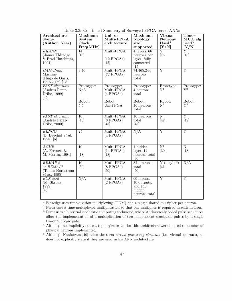
Table 3.3: Continued Summary of Surveyed FPGA-based ANNsArchitecture Maximum Uni- or Maximum Virtual Time–Name System Multi-FPGA topology Neurons MUX alg(Author, Year) Clock architecture size Used? used?
Freq(MHz) supported [Y/N] [Y/N]RRANN 14 Multi-FPGA 4 layers, 66 Y Y1
(James Eldredge [16] neurons per [15] [15]& Brad Hutchings, (12 FPGAs) layer, fully1994) [15] connected
[15]CAM-Brain 9.46 Multi-FPGA 74,465,244 Y YMachine (72 FPGAs) neurons(Hugo de Garis, total1997-2002) [12]FAST algorithm Prototype: Prototype: Prototype: Prototype: Prototype:(Andres Perez- N/A Multi-FPGA 4 neurons N4 Y2
Uribe, 1999) (4 FPGAs) total[42]
Robot: Robot: Robot: Robot: Robot:5.5 Uni-FPGA 16 neurons N4 Y3
total
FAST algorithm 10 Multi-FPGA 16 neurons N Y(Andres Perez- [45] (8 FPGAs) total [42] [42]Uribe, 2000) [45] [45]
RENCO 25 Multi-FPGA N/A Y Y(L. Beuchat et al, (4 FPGAs)1998) [5]
ACME 10 Multi-FPGA 1 hidden N4 N(A. Ferrucci & (14 FPGAs) layer, 14 [30] [18]M. Martin, 1994) [18] [18] neurons total
[30]REMAP-β 10 Mutli-FPGA 32 neurons Y (maybe5) N/Aor REMAP3 [50] (8 FPGAs) total [41](Tomas Nordstrom [50] [50]et al., 1995)ECX card N/A Mutli-FPGA 60 inputs, Y Y(M. Skrbek, (2 FPGAs) 10 outputs,1999) and 140[48] hidden
neurons total
1 Eldredge uses time-division multiplexing (TDM) and a single shared multiplier per neuron.2 Perez uses a time-multiplexed multiplication so that one multiplier is required in each neuron.3 Perez uses a bit-serial stochastic computing technique, where stochasticaly coded pulse sequences
allow the implementation of a multiplication of two independent stochastic pulses by a singletwo-input logic gate.
4 Although not explicitly stated, topologies tested for this architecture were limited to number ofphysical neurons implemented.
5 Although Nordstrom [40] coins the term virtual processing elements (i.e. virtual neurons), hedoes not explicitly state if they are used in his ANN architecture.
47
Chapter 4
Non-RTR FPGA Implementation
of an ANN.
4.1 Introduction
Certain design tradeoffs exist which must be dealt with in order to achieve fine-grain logic on
FPGAs. For range-precision vs. area in particular, the problem is twofold: how to balance
between the need of reasonable numeric precision, which is important for network accuracy
and speed of convergence, and the cost of more logic (i.e. FPGA resources) associated
with increased precision; how to choose a suitable numerical representation whose dynamic
range is large enough to guarantee that saturation will not occur for a particular application.
Floating-point would be the ideal numeric representation to use because it offers the greatest
amount of dynamic range, making it suitable for any application. This is the very reason
why floating-point representation is used in most general-purpose computing platforms.
However, due to the limited resources available on an FPGA, floating-point may not be as
feasible compared to more area-efficient numeric representations, such as fixed-point.
Artificial Neural Networks (ANNs) implemented on Field Programmable Gate Arrays
(FPGAs) have traditionally used a minimal allowable range-precision of 16-bit fixed-point.
48
This approach is considered to be an optimal range-precision vs area tradeoff for FPGA
based ANNs because quality of performance is maintained, while making efficient use of the
limited hardware resources available in a FPGA. However, limited precision of 16-bit allows
for quantization errors in calculations, while the limited dynamic range of fixed-point poses
risk of saturation. If 16-bit fixed-point is used, an engineer must deal with both of these
problems when testing and validating circuits. On the other hand, 32-bit floating-point
offers greater dynamic range and limits quantization errors, both of which make this form
of numerical representation more suitable in any application.
This chapter looks to determine the feasibility of using floating-point arithmetic in the
implementation of the backpropagation algorithm, using today’s single FPGA-based plat-
forms and related tools. In Section 4.2 various numerical representations of FPGA-based
ANNs are discussed. Section 4.3 summarizes the digital VLSI design of the backpropagation
algorithm, which was used as a common benchmark for evaluating the performance of the
floating-point and fixed-point arithmetic architectures. Validation of the proposed imple-
mentations, and benchmarked results of floating-point and fixed-point arithmetic functions
implemented on a FPGA are given in Section 4.4. Fixed-point and floating-point perfor-
mance in FPGA-based ANNs are also evaluated in comparison with an equivalent software-
based ANN. Section 4.5 summarizes the results of this investigation, and discusses how
they better reconfigurable computing as a platform for accelerating ANN testing. Limita-
tions of the proposed FPGA-based ANN architecture and ongoing design/implementation
challenges are discussed.
4.2 Range-Precision vs. Area Trade-off
One way to help achieve the density advantage of reconfigurable computing over general-
purpose computing is to make the most efficient use of the hardware area available. In
terms of an optimal range-precision vs area trade-off, this can be achieved by determining
the minimum allowable precision and minimum allowable range, where their criterion is
49
to minimize hardware area usage without sacrificing quality of performance. These two
concepts combined can also be referred to as the minimum allowable range-precision.
Because a reduction in precision introduces more error into the system, minimum allow-
able precision is actually a question of determining the maximum amount of uncertainty
(i.e. quantization error due to limited precision) an application can withstand before perfor-
mance begins to degrade. Likewise, by limiting the dynamic range there is an increase risk
that saturation may occur. Minimum allowable range is actually a question of determin-
ing the maximum amount of uncertainty (i.e. error due to saturation) an application can
withstand before performance begins to degrade. Hence, determining a minimum allowable
range-precision and suitable numeric representation to use in hardware is often dependent
upon the application at hand, and the algorithm used [40].
Fortunately, suitable range-precision for backpropagation-based ANNs has already been
empirically determined in the past. Holt and Baker [22] showed that 16-bit fixed-point was
the minimum allowable range-precision for the backpropagation algorithm. The minimum
allowable range-precision for the backpropagation algorithm minimizes the hardware area
used, without sacrificing the ANN’s ability to learn.
While 16-bit precision complements the density advantage found in FPGA based ANNs,
the quantization error of 32-bit precision is negligible. Without having to worry about
dealing with quantization error, the use of 32-bit precision helps reduce overhead in testing
and validation, and its use is justifiable if the relative loss in processing density is negligible
in comparison.
In a similar manner, fixed-point adds to the density advantage of FPGA based ANNs,
whereas the vast dynamic range of floating-point eliminates risk of saturation. In fact,
Ligon III et al. [26] have previously validated the density advantage of fixed-point over
floating-point for older generation Xilinx 4020E FPGAs, by showing that the space/time
requirements for 32-bit fixed-point adders and multipliers were less than that of their 32-bit
floating-point equivalents.
Since the size of a FPGA-based ANN is proportional to the multiplier used, it’s fair to
50

postulate that given a fixed area ’X’ on older generation FPGAs, a 32-bit signed (2’s comple-
ment) fixed-point ANN could house more neurons than a 32-bit IEEE floating-point ANN.
However, FPGA architectures and related development tools have become increasingly so-
phisticated in more recent years, including improvements in the space/time optimization
of arithmetic circuit designs. Perhaps the latest FPGA technology may have helped nar-
row the range-precision vs. area trade-off to the point where the benefits of using 32-bit
floating-point outweigh the increased density advantage that 16-bit fixed-point might still
have in comparison. As such, the objective of this chapter is to determine the feasibility of
floating-point arithmetic in ANNs using today’s FPGA technologies.
Both floating-point and fixed-point precision are considered for the FPGA-based ANN
implementation presented here, and are classified as position-dependent digital numeric
representations. Other numeric representations, such as digital frequency-based [21] and
analog were not considered because they promote the use of low precision, which is often
found to be inadequate for minimum allowable range-precision.
4.3 Solution Methodology
4.3.1 FPGA-based ANN Architecture Overview
The digital ANN architecture proposed here is an example of a non-RTR (run-time recon-
figuration) reconfigurable computing application, where all stages of the algorithm reside
together on the FPGA at once. A finite state machine was used to ensure proper sequential
execution of each step of the backpropagation algorithm as described in Section 2.4.2, which
consists of the following two states:
1. Forward state (F) - used to emulate the forward pass associated with the backprop-
agation algorithm. Only the ANN’s input signals, synapses, and neurons should be
active in this state, in order to calculate the ANN’s output. All forward pass opera-
tions (i.e. Forward Computations as described by Equations 2.6, 2.7, and 2.8) should
51

be completed by time the Forward State (F) ends.
2. Backward state (B) - used to emulate the backward pass associated with the back-
propagation algorithm. All the circuitry associated with helping the ANN learn (i.e.
essentially all the circuitry not active in Forward State) should be active here. All
backward pass operations (i.e. Backward Computations as described by Equations
2.9, 2.10, and 2.12) should be completed by time the Backward state ends.
It should be noted that both states of the finite state machine continually alternate, and
synaptic weights are updated (as described in Equation 2.13) during the transition from
Backward State to Forward State.
As far as the ANN’s components (eg. neurons, synapses) were concerned, the finite state
machine is generally a means of synchronizing when various sets of components should be
active. The duration of each state depends on the number of clock cycles required to
complete calculations in each state, the length of the system’s clock period, and the propa-
gation delay associated with each state1. The architecture of the active ANN components
associated with each state dictates the propagation delay for that state.
Each of the ANN components implemented in hardware, such as the synapse and neu-
ron, housed a chip select input signal in their architecture which is driven by the finite state
machine. This chip select feature ensured that only those components that were associated
with a particular state, were enabled or active throughout that state’s duration. With re-
gards to initialization of the circuit, the proposed FPGA-based ANN architecture was fitted
with a reset input signal, which would fulfill two important requirements when activated:
• Ensure the finite state machine initially starts in ’Forward State’.
• Initialize the synaptic weights of the ANN, to some default value.
1Note that propagation delay is platform dependent, and can only be determined after the digital VLSIdesign has been synthesized on a targeted FPGA. The propagation delay is then determined through atiming analysis/simulation using the platform’s EDA tools.
52
With all the synchronization and initialization taken care of, the only requirement left
for the FPGA-based ANN to satisfy was performing the typical calculations seen in the
backpropagation algorithm. In hardware, Equations 2.6–2.13 are realized using a series of
arithmetic components, including addition, subtraction, multiplication, and division. Stan-
dardized high-description language (HDL) libraries for digital hardware implementation can
be used in synthesizing all the arithmetic calculations involved with the backpropagation
algorithm, in analogous fashion of how typical math general programming language (GPL)
libraries are used in software implementations of ANNs. The FPGA-based ANN archi-
tecture described here is generic enough to support arithmetic HDL libraries of different
position-dependent signal representations, whether it be floating-point or fixed-point.
4.3.2 Arithmetic Architecture for FPGA-based ANNs
The FPGA-based ANN architecture was developed using a standardized HDL for digital
VLSI, known as VHDL. Unfortunately, there is currently no explicit support for fixed- and
floating-point arithmetic in VHDL2. As a result, two separate arithmetic VHDL libraries
were custom designed for use with the FPGA-based ANN. One of the libraries supports
the IEEE-754 standard for single-precision (i.e. 32-bit) floating-point arithmetic, and is re-
ferred to as uog fp arith, which is an abbreviation for University of Guelph Floating-Point
Arithmetic. The other library supports 16-bit fixed-point arithmetic, and is referred to as
uog fixed arith, which is an abbreviation for University of Guelph Fixed-Point Arithmetic.
Fixed-point representation is actually signed 2’s complement binary representation,
which is made rational with a virtual decimal point. The location of the virtual deci-
mal point is up to the discretion of the engineer, yet has no effect on the hardware used to
do the math. As suggested by Holt and Baker [22], the virtual decimal point location used
in uog fixed arith is SIII.FFFFFFFFFFFF , where
S = sign bit
2According to the IEEE Design Automation Standards Committee [3], an extension of IEEE Std 1076.3has been proposed to include support for fixed- and floating-point numbers in VHDL, and is to be addressedin a future review of the standard
53

I = integer bit, as implied by location of decimal point
F = fraction bit, as implied by location of decimal point
The range for a 16-bit fixed-point representation of this configuration is [-8.0, 8.0), with a
quantization error of 2.44140625E-4.
Description of the various arithmetic VHDL design alternatives considered for use in
the uog fp arith and uog fixed arith libraries are summarized in Table 4.1. All HDL
designs with the word std in their name signifies that one of the IEEE standardized VHDL
arithmetic libraries was used to create them. For example, uog std multiplier was easily
created using the following VHDL syntax:
z <= x ∗ y;
where x and y are the input signals, and z the output signal of the circuit. Such a high
level of abstract design is often associated with behavioural VHDL designs, where ease of
design comes at the sacrifice of letting the FPGA’s synthesis tools dictate the fine-grain
architecture of the circuit.
On the other hand, an engineer can explicitly define the fine-grain architecture of
a circuit by means of structural VHDL and schematic-based designs, as was done for
uog ripple carry adder and uog sch adder respectively. However, having complete con-
trol over the architecture’s fine-grain design comes at the cost of additional design overhead
for the engineer.
Many of the candidate arithmetic HDL designs described in Table 4.1 were created the
Xilinx CORE Generator System. This EDA tool helps an engineer parameterize ready-made
Xilinx intellectual property (IP) designs (i.e. LogiCOREs), which are optimized for Xilinx
FPGAs. For example, uog core adder was created using the Xilinx proprietary LogiCORE
for an adder design.
Approximation of the logsig function in both, floating-point and fixed-point precision,
were implemented in hardware using separate lookup-table architectures. In particular,
54

Table 4.1: Summary of alternative designs considered for use in custom arithmetic VHDLlibraries.HDL Design Descriptionuog fp add∗ IEEE 32-bit single precision floating-point pipelined parallel adderuog ripple carry adder 16-bit fixed-point (bit-serial) ripple-carry adderuog c l addr 16-bit fixed-point (parallel) carry lookahead adderuog std adder 16-bit fixed-point parallel adder created using standard VHDL
arithmetic librariesuog core adder 16-bit fixed-point parallel adder created using Xilinx LogiCORE
Adder Subtracter v5.0uog sch adder 16-bit fixed-point parallel adder created using Xilinx ADD16
schematic-based designuog pipe adder 16-bit fixed-point pipelined parallel adder created using Xilinx
LogiCORE Adder Subtractor v5.0uog fp sub∗ IEEE 32-bit single precision floating-point pipelined parallel sub-
tracteruog par subtracter 16-bit fixed-point carry lookahead (parallel) subtracter, based on
uog std adder VHDL entityuog std subtracter 16-bit fixed-point parallel subtracter created with standard VHDL
arithmetic librariesuog core subtracter 16-bit fixed-point parallel subtracter created using Xilinx Logi-
CORE Adder Subtracter v5.0uog fp mult∗ IEEE 32-bit single precision floating-point pipelined parallel mul-
tiplieruog booth multiplier 16-bit fixed-point shift-add multiplier based on Booth’s algorithm
(with carry lookahead adder)uog std multiplier 16-bit fixed-point parallel multiplier created using standard VHDL
arithmetic librariesuog core bs mult 16-bit fixed-point bit-serial (non-pipelined) multiplier created using
Xilinx LogicCORE Multiplier v4.0uog pipe serial mult 16-bit fixed-point bit-serial (pipelined) multiplier created using Xil-
inx LogiCORE Multiplier v4.0uog core par multiplier 16-bit fixed-point parallel (non-pipelined) multiplier created using
Xilinx LogiCORE Multiplier v4.0uog pipe par mult 16-bit fixed-point parallel (pipelined) multiplier created using Xil-
inx LogiCORE Multiplier v4.0
active func sigmoid Logsig (i.e. sigmoid) function with IEEE 32-bit single precisionfloating-point
uog logsig rom 16-bit fixed-point parallel logsig (i.e. sigmoid) function createdusing Xilinx LogiCORE Single Port Block Memory v4.0
∗ Based on VHDL source code dontated by Steven Derrien ([email protected]) from Insti-tut de Recherche en Informatique et systemes aleatoires (IRISA) in France. In turn, StevenDerrien had originally created this through the adaptation of VHDL source code found athttp://flex.ee.uec.ac.jp/ yamaoka/vhdl/index.html.
55
active func sigmoid was a modular HDL design, which encapsulated all the floating-
point arithmetic units necessary to carry out calculation of logsig function. According
Equation 2.8, this would require the use of a multiplier, adder, divider, and exponential
function. As a result, active func sigmoid was realized in VHDL using uog fp mult,
uog fp add, , a custom floating-point divider called uog fp div, and a table-driven floating-
point exponential function created by Bui et al [7].
The uog logsig rom HDL design utilized a Xilinx LogiCORE to implement single port
block memory. A lookup-table of 8192 entries was created with this memory, which was
used to approximate the logsig function in fixed-point precision.
In order to maximize the processing density of the digital VLSI ANN design proposed
in Section 4.3.1, only the most area-optimized arithmetic HDL designs offered in Table 4.1
should become part of the uog fp arith and uog fixed arith VHDL libraries. However,
the space-area requirements of any VHDL design will vary from one FPGA architecture
to the next. Therefore, all the HDL arithmetic designs found in Table 4.1 have to be
implemented on the same FPGA as was targeted for implementation of the digital VLSI
ANN design, in order to determine the most area-efficient arithmetic candidates. All that
remains is to decide on an example application that can be used to evaluate and compare
the performance of the various FPGA-based ANNs.
4.3.3 Logical-XOR problem for FPGA-based ANN
The logical-XOR problem is a classic example application used to benchmark the learning
ability of an ANN. In this application, the ANN is trained in an attempt to learn the logical-
XOR function, as shown in Table 4.2. The logical-XOR function is a simple example of a
non-linearly separable problem.
The minimum ANN toplogy3 required to solve a non-linearly separable problem consists
of at least one hidden layer. Hidden layers give an ANN the ability of non-linear per-
3A topology includes the number of neurons, number of layers, and the layer interconnections (i.e.synapses).
56

Table 4.2: Truth table for logical-XOR function.Inputs Outputx0 x1 y0 0 00 1 11 0 11 1 0
formance4. An overview of the ANNs topology used in this particular application, which
consists of only one hidden layer, is shown in Figure 4.1.
Input1
Input2
Output
Bias2 (b2)
Bias1 (b1)
Bias3 (b3)Neuron1
Neuron2
Neuron3
Input
Layer
Hidden
LayerOutput
Layer
W11
W22
W12
W21
W31
W32
Figure 4.1: Topology of ANN used to solve logic-XOR problem.
For ANN learning , it was best to use sequential mode training [20], as opposed to bach
mode training, because despite the fact that sequential mode converges to a solution at a
slower rate than that of batch mode, sequential mode training is the more likely of the two
to converge towards a correct solution.
For each ANN implementation, a set of thirty training sessions were performed individu-
ally. Each training session lasted for a length of 5000 epoch, and used a learning rate of 0.3.
Each of the training sessions in the set used slightly different initial conditions, in which all
weights and biases were randomly generated with a mean of 0, and a standard deviation of
4ANNs without hidden layers are known as perceptrons, and can only solve linearly-separable problems.
57
±0.3. Once generated, every ANN implementation was tested using the same set of thirty
training sessions. This way, the logical-XOR problem discussed acts as a common testing
platform, used to benchmark the performance of all ANN implementations.
Xilinx Foundation ISE 4.1i EDA tools were used to synthesize, and map (i.e. place and
route) two variations of the FPGA-based ANN designs – one using uog fp arith library,
and one using uog fixed arith library. All this, plus simulation were carried out on a PC
workstation running Windows NT (SP6) operating system, with 1 GB of memory and Intel
PIII 733MHz CPU.
These circuit designs were tested and validated in simulation only, using ModelTech’s
ModelSIM SE v5.5. Functional simulations were conducted to test the syntactical and
semantical correctness of HDL designs, under ideal FPGA conditions (i.e. where no propa-
gation delay exists). Timing simulations were carried out to validate the HDL design under
non-ideal FPGA conditions, where propagation delays associated with the implementation
as targeted on a particular FPGA are taken into consideration.
Specific to VHDL designs, timing simulations are realized using and IEEE standard
called VITAL (VHDL Initiative Toward ASIC Libraries). VITAL libraries contain informa-
tion used for modelling accurate timing of a particular FPGA at the gate level, as determined
a priori by the respective FPGA manufacturer. These VITAL libraries are then used by
HDL simulators, such as ModelSIM SE, to validate designs during timing simulations.
A software implementation of a backpropagation algorithm was created using MS Visual
C++ v6.0 IDE. Just like the FPGA-based ANNs, the software-based ANN was set up
to solve the logical-XOR problems using the topology shown in Figure 4.1. Purpose for
creating the software-based ANN was twofold: to generate expected results for testing and
validating FPGA-based ANNs; to demonstrate ANN performance on a general-purpose
computing platform. To speed up development and testing of FPGA-based ANNs, two other
software utilities were created to automate numeric format conversions–one for converting
real decimal to/from IEEE-754 single precision floating-point hexadecimal format, and one
for converting real decimal to/from 16-bit fixed-point binary format.
58
4.4 Numerical Testing/Comparison
4.4.1 Comparison of Digital Arithmetic Hardware
All the various arithmetic HDL designs considered for use in the FPGA-based ANNs were
implemented on Xilinx FPGAs, The resulting space-time requirements for each arithmetic
HDL design are summarized in Table 4.3.
In order to maximize the neuron density of the FPGA-based ANN , the area of the
various arithmetic HDL designs that a neuron is comprised of should be minimized. As a
result, the focus here is to determine the most area-optimized arithmetic HDL designs for
use in the FPGA-based ANN implementations
Comparison of the different adder results, shown in Table 4.3, reveals that the three
carry lookahead adders (i.e. uog std adder, uog core adder, and uog sch adder) require
the least amount of area and are the fastest among all non-pipelined adders. Note that
the sophistication of today’s EDA tools have allowed the VHDL-based designs for carry
lookahead adders to achieve the same fine-grain efficiency their equivalent schematic-based
designs.
Since a carry lookahead adder is essentially a ripple-carry adder with additional logic,
it isn’t immediately clear why a carry lookahead adder is shown here to use less area
compared to a ripple-carry adder when implemented on a Xilinx Virtex-E FPGA. It turns
out the Virtex-E CLBs contain dedicated fast lookahead logic that’s meant to accelerate
carry lookahead adder performance. As a result, it’s best to use HDL adder designs which
take advantage of the Virtex-E’s fast carry lookahead logic.
The Virtex-E’s fast carry-lookahead logic is again utilized to produce the best area-
optimized subtractors (i.e. uog std subtracter and uog core subtracter), as well as,
the best area-optimized multiplier (i.e. uog booth multiplier).
Only the most area-optimized arithmetic HDL designs discussed here were used in the
construction of custom arithmetic HDL libraries, as listed in Table 4.4. In the case were
59
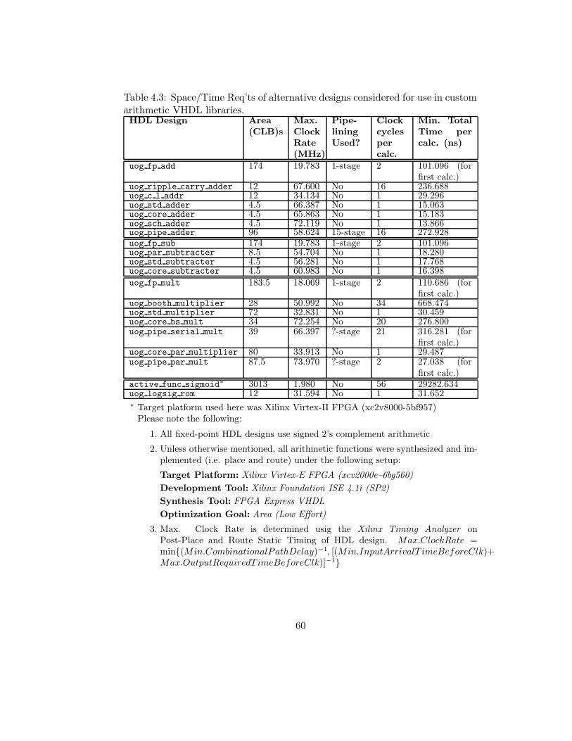
Table 4.3: Space/Time Req’ts of alternative designs considered for use in customarithmetic VHDL libraries.HDL Design Area
(CLB)sMax.ClockRate(MHz)
Pipe-liningUsed?
Clockcyclespercalc.
Min. TotalTime percalc. (ns)
uog fp add 174 19.783 1-stage 2 101.096 (forfirst calc.)
uog ripple carry adder 12 67.600 No 16 236.688uog c l addr 12 34.134 No 1 29.296uog std adder 4.5 66.387 No 1 15.063uog core adder 4.5 65.863 No 1 15.183uog sch adder 4.5 72.119 No 1 13.866uog pipe adder 96 58.624 15-stage 16 272.928uog fp sub 174 19.783 1-stage 2 101.096uog par subtracter 8.5 54.704 No 1 18.280uog std subtracter 4.5 56.281 No 1 17.768uog core subtracter 4.5 60.983 No 1 16.398
uog fp mult 183.5 18.069 1-stage 2 110.686 (forfirst calc.)
uog booth multiplier 28 50.992 No 34 668.474uog std multiplier 72 32.831 No 1 30.459uog core bs mult 34 72.254 No 20 276.800uog pipe serial mult 39 66.397 ?-stage 21 316.281 (for
first calc.)uog core par multiplier 80 33.913 No 1 29.487uog pipe par mult 87.5 73.970 ?-stage 2 27.038 (for
first calc.)active func sigmoid∗ 3013 1.980 No 56 29282.634uog logsig rom 12 31.594 No 1 31.652∗ Target platform used here was Xilinx Virtex-II FPGA (xc2v8000-5bf957)
Please note the following:
1. All fixed-point HDL designs use signed 2’s complement arithmetic
2. Unless otherwise mentioned, all arithmetic functions were synthesized and im-plemented (i.e. place and route) under the following setup:
Target Platform: Xilinx Virtex-E FPGA (xcv2000e–6bg560)
Development Tool: Xilinx Foundation ISE 4.1i (SP2)
Synthesis Tool: FPGA Express VHDL
Optimization Goal: Area (Low Effort)
3. Max. Clock Rate is determined usig the Xilinx Timing Analyzer onPost-Place and Route Static Timing of HDL design. Max.ClockRate =min{(Min.CombinationalPathDelay)−1, [(Min.InputArrivalT imeBeforeClk)+Max.OutputRequiredT imeBeforeClk)]−1}
60

there was more than one choice of best area-optimized arithmetic HDL design to choose
from, behavioural VHDL designs were preferred because they promote high-level abstract
designs and portability. For example, such was the case in selecting a fixed-point adder and
subtracter for the uog fixed arith library.
Table 4.4: Area comparison of uog fp arith vs. uog fixed arith.Arithmetic uog fixed arith uog fp arith Area OptimizationFunction HDL Design HDL Design (CLB/CLB)Adder uog std adder uog fp add 38.66x smallerSubtracter uog std subtracter uog fp sub 38.66x smallerMultiplier uog booth multiplier uog fp mult 6.55x smallerLogsig Function uog logsig rom activ func sigmoid 251.08x smaller
Table 4.4 also reveals how much more area-optimized the individual fixed-point arith-
metic HDL designs in uog fixed arith were compared to the floating-point arithmetic
HDL designs in uog fp arith. Since a floating-point adder is essentially a fixed-point
adder plus additional logic, not to mention the fact that floating-point uses more precision
than fixed-point arithmetic, it’s no surprise to find that the 16-bit fixed-point adder is much
smaller than the 32-bit floating-point adder. Similar in nature is the case for subtracter
and multiplier comparisons shown in Table 4.4.
The comparison of area-optimized logsig arithmetic HDL designs reveal that the 32-bit
floating-point version is over 250 times bigger than the 16-bit fixed-point version. Aside
from the difference in amount of precision used, the significant size difference between
logsig implementations is due the fact that floating-point implementation encapsulates a
table-lookup architecture in addition to other area-expensive arithmetic units, while the
fixed-point version only encapsulates a table-lookup via memory.
Uog fp arith and uog fixed arith have been clearly defined with only the best area-
optimized components, as shown in Table 4.4. This will help
to ensure that 32-bit floating-point and 16-bit fixed-point FPGA-based ANN implemen-
tations achieve a processing density advantage over the software-based ANN. As was shown
here, the larger area requirements of floating-point precision in FPGA-based ANNs makes
it not nearly as feasible as fixed-point precision.
61
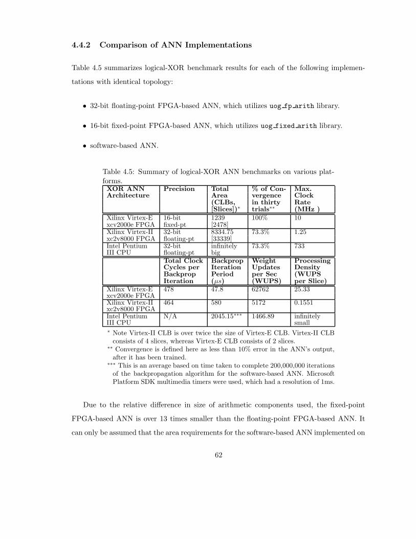
4.4.2 Comparison of ANN Implementations
Table 4.5 summarizes logical-XOR benchmark results for each of the following implemen-
tations with identical topology:
• 32-bit floating-point FPGA-based ANN, which utilizes uog fp arith library.
• 16-bit fixed-point FPGA-based ANN, which utilizes uog fixed arith library.
• software-based ANN.
Table 4.5: Summary of logical-XOR ANN benchmarks on various plat-forms.XOR ANN Precision Total % of Con- Max.Architecture Area vergence Clock
(CLBs, in thirty Rate[Slices])∗ trials∗∗ (MHz )
Xilinx Virtex-E 16-bit 1239 100% 10xcv2000e FPGA fixed-pt [2478]Xilinx Virtex-II 32-bit 8334.75 73.3% 1.25xc2v8000 FPGA floating-pt [33339]Intel Pentium 32-bit infinitely 73.3% 733III CPU floating-pt big
Total Clock Backprop Weight ProcessingCycles per Iteration Updates DensityBackprop Period per Sec (WUPSIteration (µs) (WUPS) per Slice)
Xilinx Virtex-E 478 47.8 62762 25.33xcv2000e FPGAXilinx Virtex-II 464 580 5172 0.1551xc2v8000 FPGAIntel Pentium N/A 2045.15∗∗∗ 1466.89 infinitelyIII CPU small∗ Note Virtex-II CLB is over twice the size of Virtex-E CLB. Virtex-II CLB
consists of 4 slices, whereas Virtex-E CLB consists of 2 slices.∗∗ Convergence is defined here as less than 10% error in the ANN’s output,
after it has been trained.∗∗∗ This is an average based on time taken to complete 200,000,000 iterations
of the backpropagation algorithm for the software-based ANN. MicrosoftPlatform SDK multimedia timers were used, which had a resolution of 1ms.
Due to the relative difference in size of arithmetic components used, the fixed-point
FPGA-based ANN is over 13 times smaller than the floating-point FPGA-based ANN. It
can only be assumed that the area requirements for the software-based ANN implemented on
62
a Intel PIII CPU (i.e. general-purpose computing platform) is infinitely big in comparison
to the FPGA-based ANNs.
Of concern was the fact that timing simulations via ModelSIM SE v5.5 required two
weeks for floating-point and six days for fixed-point FPGA-based ANNs just to complete
one training session in each. In general, any VLSI design which is not area-optimized may
impede the design and test productivity.
The fact that all three ANN implementations converged at all is enough to validate
the successful design of each. Note that ANNs are not always guaranteed to converge
towards a correct solution for non-linearly separable problems. Numerically speaking, the
gradient descent of an ANN might get trapped in local minima, which exists in these
kinds of problems. Just because the 16-bit fixed-point ANN implementation had a higher
convergence rate than the other two ANN implementations does not imply that it’s quality
of performance is necessarily better; only the same.
What’s interesting about the convergence percentages given in Table 4.5 is that they’re
the same for the software-based and 32-bit FPGA-based ANNs, but not for the 16-bit
FPGA-based ANNs. The software-based ANN and FPGA-based ANN that used uog fp arith
achieved the same convergence percentages because they both use 32-bit floating-point cal-
culations, and will follow identical paths of gradient descent when given the same initial
ANN parameters. Due to the quantization errors found in 16-bit fixed-point calculations, its
respective FPGA-based ANN will follow down a slightly different path of gradient descent
when exposed to the same initial ANN parameters as the other two implementations.
In the context of ANN applications, reconfigurable computing looks to increase the
neuron density above and beyond that of general-purpose computing. Due to the fact
that three neurons exist in the ANN topology used to solve the logical-XOR problem, and
based on the benchmarked speeds of backpropagation iteration for each particular ANN
implementation, the processing density can be calculated for each. For ANN applications,
processing density is realized as the number of weight updates per unit of space-time. As
shown in Table 4.5, the relative processing density of the 16-bit fixed-point FPGA-based
63

ANN implementation is significantly higher than the 32-bit floating-point FPGA-based
ANN. This reveals how a combination of minimum allowable range-precision and greater
degree of area-optimization found in 16-bit fixed-point version of the FPGA-based ANN
compared to the 32-bit fixed-point version had a direct impact on the processing density in
implementation.
In addition to infinitely large area requirements, the software-based ANN was shown to
be over 40x slower in comparison to the 16-bit fixed-point FPGA-based implementation.
Therefore, it can only be assumed that the relative processing density of the software-based
ANN is infinitely small in comparison to the other two implementations.
4.5 Conclusions
In general, we have shown that the choice of range-precision and arithmetic hardware archi-
tecture used in reconfigurable computing applications has a direct impact on the processing
density achieved. A minimal allowable range-precision of 16-bit fixed-point, as originally
determined by Holt and Baker [22], continues to provide the most optimal range-precision
vs. area trade-off for backprop-based ANNs implemented on today’s FPGAs.
The classic logical-XOR problem was used as a common benchmarking platform for
comparing the performance of a software-based ANN, and two FPGA-based ANNs – one
with 16-bit fixed-point precision, and the other with 32-bit floating-point precision. Despite
limited range-precision, the ANN with area-optimized fixed-point arithmetic managed to
maintain the same quality of performance (i.e. in terms of the ANNs ability to learn) as
demonstrated with floating-point arithmetic. Results showed that the fixed-point ANN
implementation was over 12x greater in speed, over 13x smaller in area, and achieved far
greater processing density compared to the floating-point FPGA-based ANN. Also, the
processing density achieved by the FPGA-based ANN with 16-bit fixed-point precision
compared to the software-based ANN best demonstrates the processing density advantage
of reconfigurable computing over general-purpose computing for this particular application.
64

As a result, floating-point precision is not as feasible as fixed-point in this type of application.
One disadvantage of using fixed-point, is that its’ limited range poses risk of saturation.
Saturation adds error to a system, the extent of which is application dependent. Fortunately,
the logical-XOR example demonstrated in this chapter still managed to achieve convergence,
despite saturation error caused by 16-bit fixed-pt with range [-8.0,8.0).
Besides the benefits related to reconfigurable computing, the area savings of using 16-bit
fixed-point rather than floating-point precision in a FPGA-based ANN helps to minimize
simulation durations when validating HDL designs. The current performance rate of digital
HDL simulators, like ModelSIM SE 5.5, is an ongoing concern. Not only does the duration
of timing simulations increase proportionally with size of the circuit being simulated, but
the magnitude of duration is in the order of ’days’ and even ’weeks’ for large VLSI HDL
designs.
Although proven successful for an isolated case, the FPGA-based ANN architecture pro-
posed here has several limitations, which makes it unfeasible for use in real-world applica-
tions. Aside from the fact that this architecture does not perform run-time reconfiguration,
and cannot reap the benefits which lie therein, it’s major limitation is that this ANN archi-
tecture has a fixed (i.e. hardwired) topology. Such an architecture prevents ANN engineers
from having the flexibility to experiment with various ANN topologies. Any attempts at
empirically deriving a suitable topology for a given application is not possible. The topol-
ogy hardwired into this non-RTR ANN architecture was known to solve the logical-XOR
example a priori. In the end, the only purpose this architecture managed to serve was to
act as a common benchmark for justifying the numeric representation, and area-optimized
arithmetic units suitable for reconfigurable computing applications (eg. backprop-based
ANNs) on today’s Xilinx FPGAs.
The next chapter will propose a new and improved ANN architecture; one which looks
to overcome limitations found in the non-RTR ANN architecture, and improve on the
tools/methodologies used to do so. Among other things, this new architecture will utilize
the area-optimized 16-bit fixed-point VHDL library demonstrated here, and will attempt
65

to maximize processing density through run-time reconfiguration (RTR).
66

Chapter 5
RTR FPGA Implementation of an
ANN.
5.1 Introduction
The FPGA-based ANN architecture presented in Chapter 4 helped demonstrate how 16-bit
fixed-point was the optimal range-precision vs. area tradeoff for backpropagation on today’s
reconfigurable computing platforms. It also showed which area-optimized arithmetic units
posed the best chance in maximizing processing density. Unfortunately, the Non-RTR ANN
architecture had the following shortcomings:
1. No run-time reconfiguration. All stages of ANN execution (i.e. feed-forward,
backpropagation and weight update) were packed into one big circuit for this design.
Hence, it was impossible to maximize processing density in this case.
2. ANN topology was fixed (i.e. hardwired). Hence, trainer can not experiment
with various topologies to optimize ANN performance (i.e. minimize error in output).
In the same respect, some challenges arose in the design methodology and implementation
approaches used. Time taken for behavioural / timing simulations using modern
67
digital HDL simulators (e.g. ModelSim) is on the order of days/weeks respec-
tively for VLSI designs. For example, it took months to test / debug the Non-RTR
ANN architecture proposed in Chapter 4. It might make more sense to pursue alternative
simulation methods / tools which don’t take as long to carry out the test / debug process.
The goal of this chapter is to overcome all of the above mentioned problems, which
will be achieved in two ways. First, a more modernized methodology which makes testing
with fixed-point much easier, whilst offering quicker simulation times, will be discussed and
utilized. Second, a new run-time reconfigurable ANN is proposed, which offers a much more
flexible / scalable architecture and supports user-defined topologies without the need for re-
synthesis. An architecture such as this would allow a trainer to easily define and test ANNs
of different shapes and sizes. Solving the above problems would ultimately strengthen the
case of using reconfigurable computing as a suitable platform for accelerating ANN testing.
Section 5.2 will introduce the benefits of using a unified systems design approach in
reconfigurable computing, as opposed to a traditional hw/sw co-design methodology. Sec-
tion 5.3 will give an overview of a new FPGA-based ANN architecture, called RTR-MANN,
who’s role is to demonstrate the performance enhancements that result from the utilization
of current-generation FPGA tools and methodologies. Section 5.4 and 5.5 will introduce
the design rationale and operation behind RTR-MANN’s memory map, and reconfigurable
stages of operation respectively. Both of these sections will help give the reader an apprecia-
tion of RTR-MANN’s technical merits. Next, a performance evaluation of RTR-MANN will
be conducted in Section 5.6 to quantify its learning capability and reconfigurable comput-
ing performance. Based on results, Section 5.7 will conclude which of RTR-MANN merits
correlate to recent improvements in tools / methodologies used.
5.2 A New Methodology for Reconfigurable Computing
The objective of this section is to establish a new methodology which will ease the design
and implementation of reconfigurable computing applications, especially ANN-based recon-
68
figurable platforms. This section will introduce a new system design methodology, which im-
proves upon the traditional hw/sw co-design methodology covered in Section 2.2.3. Clearly
explained is how a Higher-Level Language (HLL) not only supports this new methodology,
but how it acts as a solution to all traditional methodology problems. Highlights include
how a particular HLL, called SystemC, can be used to overcome some of the implementation-
specific challenges identified with the Non-RTR ANN architecture presented in Chapter 4.
It will be made evident that this new methodology (with SystemC as its’ HLL) should be
utilized for the new ANN architecture presented in this chapter, in order to prevent the
same problems from occurring.
5.2.1 System Design using High-Level Language (HLL)
”Today the biggest challenge in EDA is to resolve the incompatibility of the
hardware design methodology and the software methodology” – Gary Smith,
DataQuest’s Chief EDA analyst - Dataquest Briefing DAC 2002
A new software methodology has emerged, which overcomes traditional methodology
problems by offering a complete end-to-end system design flow; a unified hw/sw co-design
methodology. Sanguinetti and Pursley [47] argue that this new methodology is nothing more
but an evolution of traditional hw/sw co-design methodology, which attempts to fulfill the
following needs caused by legacy problems:
• General-purpose programming languages (GPLs) must be augmented to
facilitate both system modelling and hardware description. A unified hw/sw
co-design language is needed that would not only model software, but model hardware
down to and including the register-transfer level. Such a higher-level language (HLL)
could easily describe a ”virtual platform”; a high-level abstract model of an entire
system.
• High-Level Synthesis must use an augmented GPL as input and produce
output which can act as suitable input for standard hardware implementa-
69

System Def’n Phase- Explore Algorithm
- Define System
Functionality
- Write System HLL
Models
Design Phase- Integrate System Models
- Explore Optimal System
Partitions
- Verify System
Functionality
Implementation Phase- Compile SW to Object Code
- Compile HW to HDL/RTL or
FPGA (i.e. gate level)
- Explore Optimal
Implementation
Unified HW/SW Co-design Methodology
HW/SW Re-iteration
Figure 5.1: System design methodology for unified hw/sw co-design.
tion tools. High-Level Synthesis (or Architectural Synthesis [10]) provides a direct
connection between the system model and implementation. It is a necessary technol-
ogy to enable high-level modelling and top-down design for hardware systems.
Both HLL and High-Level Synthesis have only recently become a reality [10]. The
new system design methodology which utilizes these two tools is shown in Figure 5.1, and
contains the following phases:
System Definition Phase Specification of the system via HLL. What results is a higher-
level, executable model of the system that can be used to drive the design phase.
Not only does system description become more intuitive when a HLL is used, but the
HLL components used to realize each algorithm in the design can just as easily be
partitioned in hardware or software.
Design Phase This phase adopts the HLL descriptions of the system, where hw/sw co-
design is explored and simulated to determine optimal design partitioning in a unified
manner. Test vectors are created based on the system model, and used throughout
the remaining design flow stages to assure verification of system functionality.
Implementation Phase This is where hardware and software are finally implemented
according to their respective technologies. Software is compiled into object code to
run on a targeted general-purpose computing environment, whereas the hardware is
compiled from HLL into HDL to allow for optimization at the RTL level, or direct
synthesis from HLL to gate representation (e.g. EDIF or reprogrammable logic).
70

With support of HLLs and high-level synthesis, this new system methodology is much
improved compared to traditional hardware/software co-design methodologies. To be more
specific, this new methodology acts as a solution to the following traditional methodology
problems:
System Design and Partitioning Using HLLs to define the system functionality at the
algorithmic level is more intuitive and quicker to implement compared to development
at lower layers of abstraction (e.g. RTL or gate level). Optimal hw/sw partitioning is
much easier with system models since the effort taken to re-partition HLL logic blocks
from software to hardware and vice versa is trivial. Hence, performance tradeoffs of
a system model are easily discovered.
Hardware/Software Convergence HLL system models are a means of converging hw/sw
co-design into a more unified flow from start to finish. Verification and implementa-
tion are driven from the original system model. Here, hardware and software design
processes occur concurrently. Software is not as delayed/dependent on the hardware
design process since a system definition model is available for reference.
System Verification Functional verification is more intuitive, since it starts using HLL
system models based on algorithmic design. HLLs allow for co-verification of hardware
and software throughout the entire design flow. Hence, system functionality can be
assured throughout the design flow. No matter which phase of design, hardware and
software partitions within HLL system model can be easily modified or re-partitioned
as needed during the verification process.
System Implementation High-level synthesis is the missing link in traditional method-
ologies, which promotes use of HLLs for unified hw/sw co-design and co-verification.
Similar to compiling software, hardware can now be derived directly from hardware
partitions specified in the HLL system model. Designers can use this capability to
implement rapid prototypes in hardware, where design flow is sped up tremendously.
71
High-level synthesis is a crucial part of this emerging methodology, but the specific role
this technology plays is not clearly defined. The role of high-level synthesis was originally
intended for use in proof-of-concept implementations only, even though it can act as substi-
tute for lower-level (e.g. RTL/HDL) synthesis at any time [9]. Similar to software design,
an HLL promotes behavioural design since it describes systems at such as high-level of ab-
straction. On the other hand, RTL/HDL promotes structural design, which allows for more
detailed control hardware resources (i.e. area, speed, power) at the cost of longer design
times. Synthesis of behavioural designs often leads to coarse-grain logic, whereas synthesis
of structural designs leads to fine-grain logic desired in hardware optimization. The main
concern is that HLL synthesis is in its infancy, and is sub-optimal compared to RTL/HDL
synthesis. However, as high-level synthesis tools mature, they’ll tend towards producing op-
timized fine-grain logic. In future, high-level synthesis of HLLs will become an even match
for RTL/HDL synthesis tools, but with the benefit of quicker design flow.
In summary, this subsection has introduced a much improved systems design method-
ology, which can be applied to reconfigurable computing applications. Both HLL and high-
level synthesis play a major role in helping this new methodology overcome traditional
design flow problems. The next subsection will focus on a particular HLL, called SystemC,
whose features can be exploited to benefit a particular reconfigurable application, namely
ANN-based reconfigurable platforms.
5.2.2 SystemC: A Unified HW/SW Co-design Language
This subsection gives an overview of a particular HLL, called SystemC. Discussion will be
given on how SystemC’s features can be exploited to overcome some of the implementation
specific challenges identified with the Non-RTR ANN architecture.
Many HLLs1 are essentially a modified version of an existing GPL, which has added
nonproprietary extensions to describe system modelling and hardware. SystemCTMis an
1Other examples of C/C++ based HLLs include SpecC and Handel-C.
72
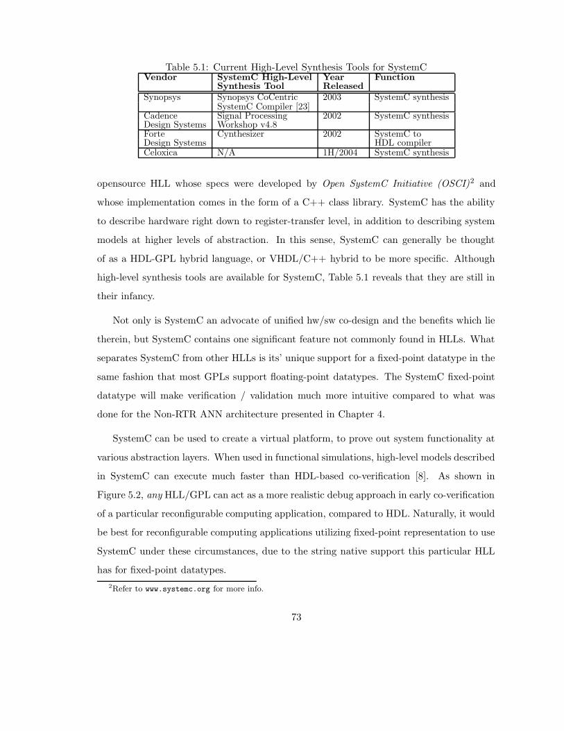
Table 5.1: Current High-Level Synthesis Tools for SystemCVendor SystemC High-Level Year Function
Synthesis Tool ReleasedSynopsys Synopsys CoCentric 2003 SystemC synthesis
SystemC Compiler [23]Cadence Signal Processing 2002 SystemC synthesisDesign Systems Workshop v4.8Forte Cynthesizer 2002 SystemC toDesign Systems HDL compilerCeloxica N/A 1H/2004 SystemC synthesis
opensource HLL whose specs were developed by Open SystemC Initiative (OSCI)2 and
whose implementation comes in the form of a C++ class library. SystemC has the ability
to describe hardware right down to register-transfer level, in addition to describing system
models at higher levels of abstraction. In this sense, SystemC can generally be thought
of as a HDL-GPL hybrid language, or VHDL/C++ hybrid to be more specific. Although
high-level synthesis tools are available for SystemC, Table 5.1 reveals that they are still in
their infancy.
Not only is SystemC an advocate of unified hw/sw co-design and the benefits which lie
therein, but SystemC contains one significant feature not commonly found in HLLs. What
separates SystemC from other HLLs is its’ unique support for a fixed-point datatype in the
same fashion that most GPLs support floating-point datatypes. The SystemC fixed-point
datatype will make verification / validation much more intuitive compared to what was
done for the Non-RTR ANN architecture presented in Chapter 4.
SystemC can be used to create a virtual platform, to prove out system functionality at
various abstraction layers. When used in functional simulations, high-level models described
in SystemC can execute much faster than HDL-based co-verification [8]. As shown in
Figure 5.2, any HLL/GPL can act as a more realistic debug approach in early co-verification
of a particular reconfigurable computing application, compared to HDL. Naturally, it would
be best for reconfigurable computing applications utilizing fixed-point representation to use
SystemC under these circumstances, due to the string native support this particular HLL
has for fixed-point datatypes.
2Refer to www.systemc.org for more info.
73
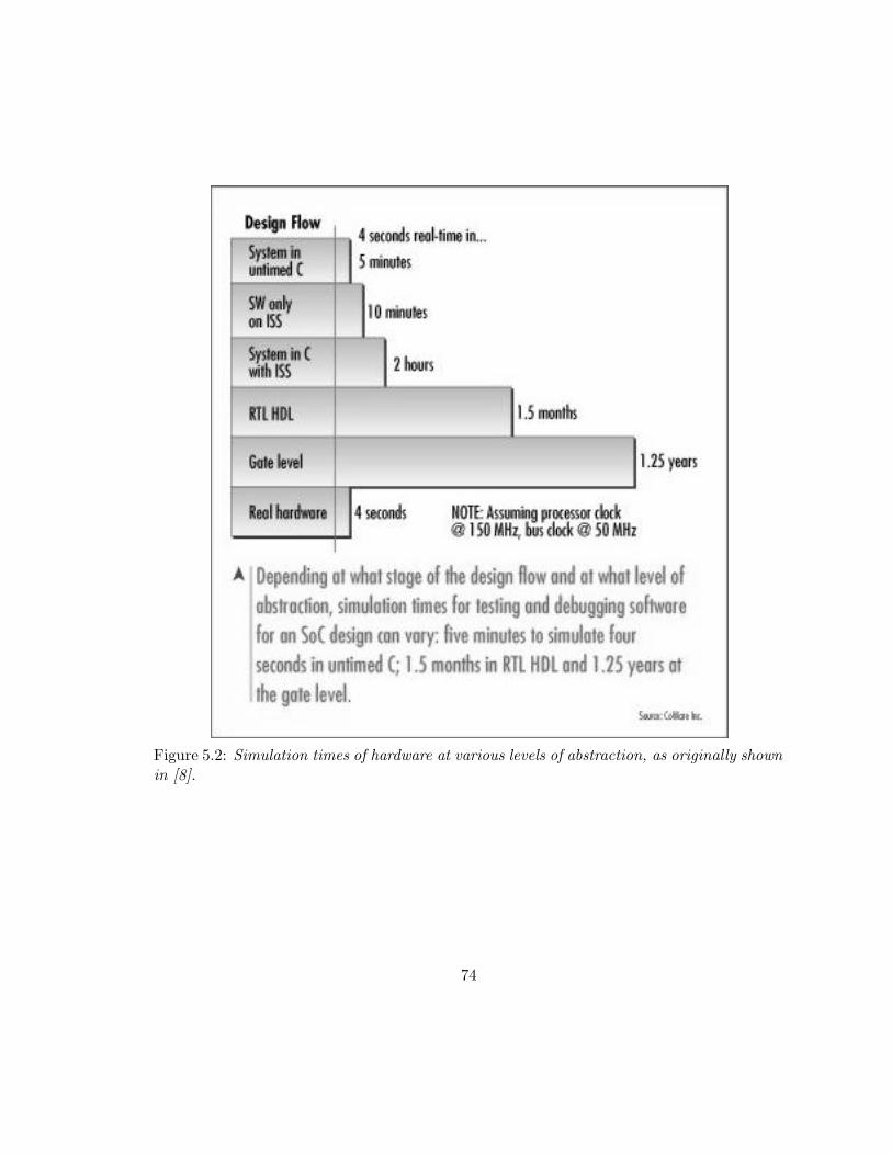
Figure 5.2: Simulation times of hardware at various levels of abstraction, as originally shownin [8].
74

In summary, this subsection has explained how SystemC’s native support for fixed-
point datatypes allows for much faster, more intuitive co-verification compared to HDL.
Not only is this the case for the Non-RTR ANN architecture, but such is the case for any
hw/sw co-design which uses fixed-point numerical representation. In fact, the RTR ANN
architecture introduced in the next section will utilize SystemC for these very reasons. If
applied, the benefits of using SystemC under the unified hw/sw co-design methodology will
help strengthen reconfigurable computing as a viable means of accelerating ANN platforms.
5.3 RTR-MANN: An Overview
This section introduces a new reconfigurable architecture for backpropagation, called RTR-
MANN3. The purpose this new architecture serves, a description of tools used in its con-
ception, and an overview of its’ operation (i.e. steps of execution) will all be addressed.
RTR-MANN is a new reconfigurable architecture which looks to improve on the short-
comings of the Non-RTR backprop architecture specified in Chapter 4. Hence, the primary
objective of RTR-MANN was to design a scalable / flexible backprop architecture that sup-
ports user-defined topologies without the need for re-synthesis. Using tools / methodologies
which allow for a faster, more intuitive verification / validation phase was RTR-MANN’s
secondary objective. In terms of reconfigurable computing, as with any architecture of this
nature, maximizing processing density was an ultimate goal for RTR-MANN.
Ideally, RTR-MANN was intended for execution on a co-processor architecture 4, where
a host computer offloads computationally intensive portions of the backpropagation algo-
rithm to a FPGA co-processor. In particular, the Celoxica RC1000-PP5 FPGA platform was
3RTR-MANN is an acronym for Run-Time Reconfigurable Modular Artificial Neural Network. Al-though its intention is to eventually support modular ANNs, the current incarnation of RTR-MANN canonly support single ANNs as demonstrated in this thesis. Please refer to [4] for more information on modularANNs
4The co-processor architecture referred to in this context is depicted in Figure 2.8 and reviewed inSubsection 3.2
5The RC1000-PP was originally designed and manufactured by Alpha Data Systems(www.alphadata.co.uk) under the name of ADC-RC1000, which Celoxica (www.celoxica.com) bought therights to sometime in 2001 and resold under its own product line.
75
targeted as RTR-MANN’s chosen co-processor for two reasons: it had the ability to perform
run-time reconfiguration, and the FPGA it housed was a Xilinx Virtex-E FPGA (xcv2000e-
6bg560) with approximately 2.5 million logic gates. Recall that the Non-RTR backprop
architecture used a custom 16-bit fixed-point arithmetic VHDL library (uog fixed arith),
which was area-optimized for this very same FPGA. Hence, an attempt to maximize process-
ing density (i.e. neuron density) for RTR-MANN is made through combined use of run-time
reconfiguration on the Celoxica RC1000-PP, and reuse of area-optimized uog fixed arith
for this particular architecture.
The Celoxica RC1000-PP is a commercial off-the-shelf PCI (33MHz) card that contains
a FPGA, 8MB (4 banks x 2MB SDRAM) on-board memory, and can achieve clock speeds
between 100–400 MHz. Low-level drivers6 for the RC1000-PP are encapsulated in a software
API, which allows a program running on the host PC to achieve the following:
• Communicate with RC1000-PP’s on-board memory banks.
• Communicate with RC1000-PP’s FPGA general I/O pins.
• Give the host PC ability to perform (run-time) reconfiguration at any time.
RTR-MANN’s system architecture is made up of the following components (as depicted
in Figure 5.3 ):
ANN Topology Definition File - This file is the means by which ANN researchers man-
ually define a topology to be executed by RTR-MANN. The ANN Topology Definition
File is simply a text file with a standardized format that ANN researchers can use to
easily assign values to all ANN topology parameters, including: learning rate; number
of layers; number of neurons in each layer; neuron weight and bias values; number of
training patterns and their corresponding values. An example of the ANN Topology
Definition File format is shown in Appendix C. The ’input’ version of this file is
6Celoxica low-level C/C++ drivers are compatible with Microsoft Windows 98/NT/2000 operating sys-tems.
76

Feed-forward
Stage
Backpropagation
Stage
Weight Update
Stage
FPGA
On-board memory
Celoxica
RC1000-PP
Host PC
SoftCU
Program
PCI Communication
(via Celoxica Low-Level Driver)
Hardwired
Communication
Run-time Reconfiguration
ANN
Topology
Definition
File
ANN
Topology
Definition
File input output
Figure 5.3: Real (Synthesized) implementation of RTR-MANN.
77
manually created by the ANN researcher, which is then parsed (using lexical analysis)
by RTR-MANN to extract all topology information at the start of execution. The
’output’ version of this file is automatically generated by RTR-MANN once execution
/ training has completed, using the latest topology parameter values stored in the
FPGA co-processor’s on-board memory.
Software Control Unit (SoftCU) - SoftCU is RTR-MANN’s main control unit; a soft-
ware program which resides on the host PC. The main objective of SoftCU is to
ensure the stages of operation are carried out in the correct order, and for the correct
number of iterations (e.g. correct number of epochs during ANN training). Ideally,
SoftCU encapsulates the Celoxica low-level driver API in order to fulfill the following
responsibilities during execution:
1. Reconfiguring Celoxica RC1000-PP - upload configuration information (i.e. a
FPGA bit file (*.bit) stored locally on the host PC’s hard drive) to the FPGA.
In order to support run-time reconfiguration, RTR-MANN will require the use
of multiple bit files; one for every stage of operation (i.e. one bit file per logic
circuit).
2. Load / Unload Celoxica RC1000-PP’s on-board memory - extract and upload the
contents of ANN Topology Definition File to on-board memory, and vise versa
when ANN execution / training has finished.
3. Synchronization with Celoxica RC1000-PP - reset the FPGA once it has been
configured to start proper execution if its logic, and detect when a given stage
of operation has completed. For each stage of operation, SoftCU will begin
execution of FPGA logic by toggling the reset signal (assigned to one of the
FPGA’s general-purpose I/O pins), then monitor a pre-defined FPGA output
pin used by the executing stage to flag when it has completed.
Three reconfigurable stages of operation - In an attempt to maximize processing den-
sity by minimizing idle circuity, the backpropagation algorithm can be split up into
78
three reconfigurable stages: feed-forward; backpropagation; and weight update.
Hence, a different logic design was created for each stage, and executed in sequential
order through run-time reconfiguration on the FPGA platform, as illustrated at the
bottom of Figure 2.1. A traditional control unit / datapath methodology was used
in the design of all three stages of operation. Common to all three stages were an
address generator (AddrGen) and memory controller (MemCont) logic units used to
properly interface with the FPGA platform’s on-board memory (in accordance with
RTR-MANN’s memory map). Consequently, SoftCU also conforms to RTR-MANN’s
memory map when interfacing with the FPGA platform’s on-board memory, by utiliz-
ing a software version of the AddrGen and MemCont logic units. Another commonality
between two out of the three stages of operation was the utilization of Eldredge’s
time-multiplexed algorithm, which is given as follows [15]:
1. First, in order to feed activation values forward, one of the neurons on
layer m places its activation value on the [interconnection] bus.
2. All neurons on layer m + 1 read this value from the bus and multiply
it by the appropriate weight storing the result.
3. Then, the next neuron in layer m places its activation value on the bus.
4. All of the neurons in layer m + 1 read this value and again multiply it
by the appropriate weight value.
5. The neurons in layer m + 1 then accumulate this product with the
product of the previous multiply.
6. This process is repeated until all of the neurons in layer m have had a
chance to transfer their activation values to the neurons in layer m+1.
In this manner, the neurons in a given layer communicate their activation
values to the next layer, as shown in Figure 5.4.
Eldredge’s time-multiplexed algorithm indirectly supports ’virtual neu-
rons’, the combination of which has allowed RTR-MANN to achieve the
scalability / flexibility needed to test ANNs of various topologies.
79

Interconnection
Bus
Hardware Neuron 1
Hardware Neuron 2
Hardware Neuron 3
Hardware Neuron M
Layer m Layer m+1
Figure 5.4: Eldredge’s Time-Multiplexed Algorithm (as originally seen in Figure 4.3 on pg.22 of [15]).
Ideally, a high-level description of RTR-MANN’s steps of execution are summarized as
follows:
1. The user manually constructs an ANN Topology Definition File for the application
80
under test.
2. The user then starts execution of SoftCU on the host PC, where the pre-defined ANN
Topology Definition File is used as input.
3. SoftCU uploads all information extracted from the ANN Topology Definition File
to the FPGA co-processor’s on-board memory (in accordance with RTR-MANN’s
memory map).
4. SoftCU reconfigures the FPGA platform with feedforward stage of operation, then
resets the corresponding logic circuit to start execution.
5. Feed-forward stage of operation reads all topology and training data from RTR-
MANN’s memory map (via AddrGen and MemCont logic units), processes this data
according to the subset of Backpropagation algorithm equations associated with the
feedforward stage, then writes the resulting output data back into RTR-MANN’s
memory map. During this time, SoftCU monitors for a ’DONE’ flag to be set in the
FPGA logic, which signifies when the feedforward stage has completed its’ phase of
operation.
6. Steps 4 and 5 are then repeated for the Backpropagation stage of operation carried
out on the FPGA platform (only if RTR-MANN is in training mode).
7. Steps 4 and 5 are then repeated for the Weight Update stage of operation carried
out on the FPGA platform (only if RTR-MANN is in training mode).
8. Repeat Steps 4–7 for each remaining input training pattern.
9. Repeat Step 8 for a total of (z − 1) iterations, where z is the number of epochs as
specified by the user. (NOTE: z = 1 if RTR-MANN is not in training mode.)
10. SoftCU will automatically write the contents of RTR-MANN’s memory map back into
an output ANN Topology Definition File, which contains ANN output (and trained
’topology’ data if RTR-MANN in training mode).
81
For this thesis, the concept of RTR-MANN was actually tested and validated using
behavioural simulations in SystemC, rather than HDL simulators. This was done with the
promise that SystemC would allow for a faster, more intuitive verification / validation
phase for RTR-MANN than was possible by HDL simulators. As a result, SystemC was
used to emulate the entire RTR-MANN system in software, where the ideal functionality of
both, Celoxica RC1000-PP’s on-board memory and uog fixed arith VHDL library, were
reproduced at the signal level (according to their respective interface specifications).
In order to emulate run-time reconfiguration in SystemC behavioural simulations, each
reconfigurable stage of operation was compiled into a separate SystemC software program,
and were autonomously executed in sequential order using a Tcl script7, as shown in Fig-
ure 5.5. The Tcl script also allowed the user to define the number of epochs to be carried
out on the ANN under test.
There is a difference in steps of execution between emulation in SystemC versus a real,
synthesized implementation of RTR-MANN running on the actual Celoxica RC1000-PP
co-processor. A problem arises only in the SystemC implementation, where the on-board
memory is effectively cleared (i.e. SystemC executable terminated) just before reconfig-
uration for the next stage occurs. This problem was remedied through automatic
generation of ANN Topology Definition File after each stage of operation, rather
than waiting until the very last stage of operation has finished. In this case, the
ANN Topology Definition File is used to temporarily store the contents of RTR-MANN’s
memory map during run-time reconfiguration.
In summary, this section has introduced a new reconfigurable architecture for backprop-
agation, which targets the Celoxica RC1000-PP (i.e. FPGA co-processor). As its name
implies, RTR-MANN utilizes run-time reconfiguration, in addition to the area-optimized
uog fixed arith library, to guarantee maximized processing density. The combined use of
Eldredge’s time-multiplexed algorithm and ’virtual neurons’ provide RTR-MANN with the
scalability / flexibility needed to support ANN topologies of any size (without the need for
7ActiveState ActiveTCL v8.4.1.0, a binary distribution of Tcl for Windows operating system was used
82

Run-t
ime
Re
co
nfig
ura
tio
n
(via
TC
L sc
rip
t)
AN
N
Top
olo
gy
De
finiti
on
File
Fee
d-f
ow
ard
Sta
ge
On-b
oa
rd
me
mo
ry
SoftC
U
Signal-level
Communication
Sys
tem
C
exe
cuta
ble
AN
N
Top
olo
gy
De
finiti
on
File
Ba
ckp
rop
Sta
ge
On-b
oa
rd
me
mo
ry
SoftC
U
Signal-level
Communication
Sys
tem
C
exe
cuta
ble
AN
N
Top
olo
gy
De
finiti
on
File
We
ight
Up
da
te
Sta
ge
On-b
oa
rd
me
mo
ry
SoftC
U
Signal-level
Communication
Sys
tem
C
exe
cuta
ble
Figure 5.5: SystemC model of RTR-MANN.83
re-synthesis). The ANN Topology Definition File was introduced as a means of specifying
user-defined topologies for RTR-MANN.
The entire system architecture has been modelled in SystemC, which promised a faster,
more intuitive verification / validation phase of design compared to HDL simulators. A TCL
script has been used to automatically execute all stages of RTR-MANN’s reconfigurable
stages of operation in sequential order, thus making TCL a tool for emulating run-time
reconfiguration during SystemC behavioural simulation.
Discrepancies found between the SystemC model versus real implementation of RTR-
MANN’s steps of execution are trivial in terms of functionality, since the SystemC model
simply required more of the same steps that already existed for the real implementation. The
next section will focus on the design specification and SystemC modelling of RTR-MANN’s
memory map, associated logic units (MemCont and AddrGen), and Celoxica RC1000-PP’s
on-board memory.
5.4 Memory Map and Associated Logic Units
This section will give details regarding RTR-MANN’s memory map, which was targeted to
reside on Celoxica RC1000-PP’s on-board memory. Next, an explanation will be given of
how this on-board memory was modelled in SystemC. Finally, an overview will be given of
the set of custom logic units built, which allowed all FPGA stages of operation to interface
with the on-board memory, in a manner that conformed with RTR-MANN’s memory map.
5.4.1 RTR-MANN’s Memory Map
RTR-MANN’s memory map was explicitly designed to stay within the constraints of the
Celoxica RC1000-PP’s on-board memory. The memory itself consists of four asynchronous
SRAM banks, each of which was constructed from four 512k x 8-bit memory chips (Cypress
CY7C1049-17VC). Concatenation of all four SRAM banks into one big conceptual memory
block gives a total memory size of 512k x 128-bits = 8Mbytes.
84
The RC1000-PP’s FPGA has four 32-bit memory ports; one for each memory bank.
Separate data, address and control signals are associated with each bank. The FPGA can
therefore access all four banks simultaneously and independently. Since RTR-MANN
uses 16-bit values, it’s memory map is thus constrained to a matrix of maximum
512k rows and (8 x 16-bit) columns, where one row of values can be accessed
simultaneously.
RTR-MANN’s memory map is shown in Figure 5.6, which is segmented into four con-
ceptual sub-blocks:
Block A - Neuron Layer Data Contains neuron data for each layer (excluding Input
Layer) and can store up to a maximum of M layers. Neuron data consists of the
weights(
w(s)kj (n)
)
, biases(
θ(s)k
)
, output(
o(s)k
)
, and local gradients(
δ(s+1)j
)
associ-
ated with each neuron in every layer. RTR-MANN’s memory map can store neuron
data for a maximum of (N + 1) neurons per layer.
Block B - Input and Output Training Patterns - This block simply stores all of the
ANN training data. In ’training’ mode, the user has to specify both the input(
o(0)k
)
and output (tk) training patterns, else just the input training data if not in ’training’
mode. This sub-block can store up to a maximum of (K +1) sets of training patterns.
Block C - Output Error - This block stores the output error(
ε(s)k
)
for each neuron in
the output layer, up to a maximum of (N + 1) neurons.
Block D - ANN Topology Data - This block stores miscellaneous topology data, which
RTR-MANN relies on to keep track of that input data that’s already been processed
through the ANN during execution, including: the Current Training Pattern, Total
Number of Patterns, Number of Non-Input Layers, and Learning Rate (η).
With the exception of Block D, all other memory sub-blocks do not have a fixed size and
are thus, dynamic in nature. Specific to the ANN application under test, the size of each
sub-block grows independent to one another. Hence, the maximum size of topology that
85
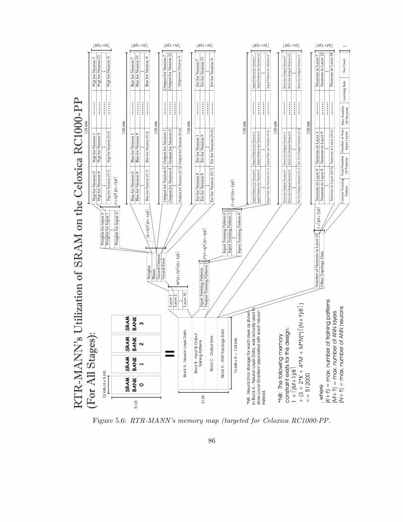
32
-bits
(4
x 8
-bit)
51
2K
SRAM
BANK
0
SRAM
BANK
1
SRAM
BANK
2
SRAM
BANK
3
12
8-b
its
51
2K
Blo
ck
A -
Ne
uro
n L
aye
r D
ata
Blo
ck
B -
Inp
ut &
Outp
ut
Tra
inin
g P
atte
rns
Blo
ck
C -
Outp
ut Erro
r
Blo
ck
D -
AN
N T
op
olo
gy
Da
ta
RT
R-M
AN
N’s
Uti
liza
tion
of
SR
AM
on
th
e C
eloxic
a R
C10
00
-PP
(For
All
Sta
ges
):
Lay
er 1
Lay
er 2
Lay
erM
Wei
gh
ts
Bia
ses
Neu
ral
Ou
tpu
t
Wei
gh
ts f
or
I np
ut
0
Wei
gh
ts f
or
I np
ut
1
Wei
gh
ts f
or
I np
ut
N
..
..
Neu
ral
Err
or
Bia
s fo
r N
euro
n 0
Bia
s fo
r N
euro
n 8
Bia
s fo
r N
euro
n (
)N
-7
..
Bia
s fo
r N
euro
n 1
Bia
s fo
r N
euro
n 9
Bia
s fo
r N
euro
n (
)N
-6
..
Bia
s fo
r N
euro
n 7
Bia
s fo
r N
euro
n 1
3
Bia
s fo
r N
euro
nN
..
......
....
....
......
....
....
Wg
t fo
r N
euro
n 0
Wg
t fo
r N
euro
n 8
Wg
t fo
r N
euro
n (
)N
-7
..
Wg
t fo
r N
euro
n 1
Wg
t fo
r N
euro
n 9
Wg
t fo
r N
euro
n (
)N
-6
..
Wg
t fo
r N
euro
n 7
Wg
t fo
r N
euro
n 1
3
Wg
t fo
r N
euro
nN
..
......
....
....
......
....
....
12
8-b
its
éù () N+1/8
(1+
N)
N+
1/8
*(
)é
ù
(4)*
()
+N
N+
1/8
éù
éù () N+1/8
M*(4
)*(
)+
NN
+1
/8é
ù
Inp
ut
Tra
inin
g P
atte
rns
Ou
tpu
t T
rain
ing
Pat
tern
s
Inp
ut
Tra
inin
g P
atte
rn 0
..
Inp
ut
Tra
inin
g P
atte
rn 1
Inp
ut
Tra
inin
g P
atte
rnK
Inp
ut
Pat
tern
fo
r N
euro
n 0
Inp
ut
Pat
tern
for
Neu
ron
8
Inp
ut
Pat
t.fo
r N
euro
n (
)N
-7
..
Inp
ut
Pat
tern
fo
r N
euro
n 1
Inp
ut
Pat
tern
for
Neu
ron
9
Inp
ut
Pat
t.fo
r N
euro
n (
)N
-6
..
Inp
ut
Pat
tern
for
Neu
ron
7
Inp
ut
Pat
tern
for
Neu
ron
13
Inp
ut
Pat
tern
for
Neu
ron
N
..
......
....
....
......
....
....
12
8-b
its
éù () N+1/8
(1+
K)
N+
1/8
*(
)é
ù
2*(1
+K)
N+
1/8
*(
)é
ù
16
-bits
x 8
= 1
28
-bits
Err
or
for
Ou
tpu
t N
euro
n 0
Err
or
for
Ou
tpu
t N
euro
n 8
Err
for
Ou
tpu
t N
euro
n (
)N
-7
..
Err
or
for
Ou
tpu
t N
euro
n 1
Err
or
for
Ou
tpu
t N
euro
n 9
Err
. Fo
r O
utp
ut
Neu
ron
()
N-6
..
Err
or
for
Ou
tpu
t N
euro
n 7
Err
or
for
Ou
tpu
t N
euro
n 1
3
Err
or
for
Ou
tpu
t N
euro
nN
..
......
....
....
......
....
....
12
8-b
its
éù () N+1/8
Nu
mb
er o
f N
euro
ns
in L
ayer
M
Oth
er T
op
olo
gy
Dat
aN
euro
ns
in L
ayer
0
Neu
ron
s in
Lay
er 8
Cu
rren
t T
rain
ing
Pat
tern
..
Neu
ron
s in
Lay
er 1
Neu
ron
s in
Lay
er 9
Neu
ron
s in
Lay
er (
)M
-6
..
Neu
ron
s in
Lay
er 7
Neu
ron
s in
Lay
er 1
3
Neu
ron
s in
Lay
erM
..
......
....
....
......
....
....
12
8-b
its
éù () M+1/8
To
tal
Nu
mb
erO
f P
atte
rns
Nu
mb
er o
f N
on
-In
pu
t L
ayer
sL
earn
ing
Rat
eM
ax N
um
ber
Of
Neu
ron
sN
ot
Use
d
1+
M+
1/8
éù
()
Ou
tpu
t fo
r N
euro
n 0
Ou
tpu
t fo
r N
euro
n 8
Ou
tpu
t fo
r N
euro
n (
)N
-7
..
Ou
tpu
t fo
r N
euro
n 1
Ou
tpu
t fo
r N
euro
n 9
Ou
tpu
t fo
r N
euro
n (
)N
-6
..
Ou
tpu
t fo
r N
euro
n 7
Ou
tpu
t fo
r N
euro
n 1
3
Ou
tpu
t fo
r N
euro
nN
..
......
....
....
......
....
....
12
8-b
its
éù () N+1/8
Err
fo
r N
euro
n 0
Err
fo
r N
euro
n 8
Err
fo
r N
euro
n (
)N
-7
..
Err
fo
r N
euro
n 1
Err
fo
r N
euro
n 9
Err
fo
r N
euro
n (
)N
-6
..
Err
fo
r N
euro
n 7
Err
fo
r N
euro
n 1
3
Err
fo
r N
euro
nN
..
......
....
....
......
....
....
12
8-b
its
éù () N+1/8
*N
B:
The
fo
llow
ing
me
mo
ry
co
nst
rain
t e
xist
s fo
r th
is d
esi
gn:
1 +
(+
1)/8
+ (3
+ 2
*+
4*
+*
)*(
()
)
<=
51
20
00
, w
he
re
() =
ma
x. n
um
be
r o
f tra
inin
g p
atte
rns
() =
ma
x. n
um
be
r o
f A
NN
laye
rs
() =
ma
x. n
um
be
r o
f A
NN
ne
uro
ns
éù
éù
M
KM
MN
N+
1/8
K+
1
M+
1
N+
1
Neu
ron
s in
Lay
er (
)M
-5
*N
B:
sto
rag
e fo
r e
ac
h la
yer a
s sh
ow
n
in B
loc
k A
- N
euro
n L
aye
r D
ata
, w
as
ac
tua
lly u
sed
to
sto
rea
sso
cia
ted
with
ea
ch n
euro
n
inst
ea
d.
Ne
ura
l Err
or
Loc
al G
rad
ient
1
Figure 5.6: RTR-MANN’s memory map (targeted for Celoxica RC1000-PP.
86
RTR-MANN can support is not fixed, and depends on the amount of training data used.
Equation 5.1 is derived in Figure 5.6, and gives a maximum size topology supported by
RTR-MANN in relation to the amount of training data used for the ANN application under
test, the combination of which is constrained by the size of RC1000-PP’s on-board memory.
1 + d(M + 1)/8e + (3 + 2 ∗ K + 4 ∗ M + M ∗ N) ∗ d(N + 1)/8e ≤ 512000 (5.1)
, where
(K + 1) = Maximum Number of Training Patterns
(M + 1) = Maximum Number of ANN Layers
(N + 1) = Maximum Number of ANN Neurons
The benefit of RTR-MANN’s dynamic memory map is that it makes more efficient use of
Celoxica RC1000-PP’s on-board memory (compared to a static memory map). As a result,
the scalability / flexibility designed into this dynamic memory map allows RTR-MANN to
support a greater number of ANN applications with different combinations of topology size
and amount of training data used.
5.4.2 SystemC Model of On-board Memory
Behavioural simulation of the FPGA co-processor’s on-board memory was performed in
SystemC. This was achieved by implementing the on-board memory as a SystemC ’object’
according to its signal-level interface specification and functional characteristics, as outlined
in the Celoxica RC1000-PP hardware reference manual [28]. Ideally, the intention was to
model each SRAM memory bank as a 512k variable array of sc lv< 32 > (i.e. a 32-
bit logic vector datatype); a datatype equivalent to the STD LOGIC VECTOR declaration in
VHDL. This array was then encapsulated in a SystemC ’object’, called RC1000 mem bank,
along with a logic signal interface that corresponded to the SRAM banks’ dedicated address
bus, data bus, and control signals. However, it turned out that the SystemC run-time kernel
87

was only able to support sc lv< 32 > arrays with a maximum of 5120 nodes8. This meant
that the maximum size of RTR-MANN’s dynamic memory map was smaller than originally
anticipated, but was still sufficient enough to conduct the behavioural simulations needed
to prove out this architecture. All that remained was to create the necessary logic in the
FPGA fabric that could properly interface with four instances of RC1000 mem bank.
5.4.3 MemCont and AddrGen
Eight 16-bit registers (MB0-MB7) were created on the FPGA to send / receive data in con-
junction with the on-board memory, as shown in Figure 5.7. MB0-MB7 were implemented
as instances of a SystemC ’object’ called uog register, which contained custom logic used
to emulate the generic behaviour of a register. However, it was later discovered that a
simpler approach would have been to implement each register using a ’signal’ declaration9
in SystemC, just like VHDL.
Registers (MB0-MB7) were divided into four sets of pairs, where each pair were mapped
and routed to the 32-bit data port of a different SRAM bank. Hence, all memory buffer
(MB0-MB7) registers could be written to / read simultaneously by a corresponding row in
the 512k x 128-bit memory block. In a similar manner, the individual address and control
signals for each SRAM bank was mapped and routed to RTR-MANN’s memory controller
unit (MemCont), which resides on the FPGA. When provided with an address, MemCont
would perform the necessary signalling (according to the SRAM bank read / write / access
timing models specified in Celoxica RC1000-PP’s H/W manual [28]) to ensure that the entire
memory row being addressed was properly transferred into the FPGA’s local memory buffer
(MB0-MB7) registers during a read operation, or vice versa for a write operation.
RTR-MANN’s address generator (AddrGen) is responsible for determining an on-board
8More specifically, the instantiation of sc lv< 32 > RC1000 mem bank[512000] object would causeSC METHOD memory stack to overflow, and generate an ’UNKNOWN ERROR EXCEPTION’ in the SystemC run-time kernel (version 2.0.1). The array size had to be shrunk down to 5120 in order to allow tracing to occurwhen the testbench ran.
9A ’signal’ is represented by the sc signal<> declaration in SystemC, which is equivalent to the SIGNAL
in VHDL.
88
memory address, which corresponds to the kind of topology data the FPGA stage of opera-
tion wants to have accessed. The resultant address can then be used as input into MemCont.
Hence, the combined functionality of MemCont and AddrGen provide an automated mecha-
nism in the FPGA fabric to access the on-board memory in conformance to RTR-MANN’s
memory map. Like all of the custom FPGA logic defined for this system, the design of
MemCont and AddrGen were both based on the control unit / datapath paradigm. Modelling
of MemCont, AddrGen, and memory data registers weren’t an issue, since implementation of
this paradigm in SystemC is very similar10 to how it would be done in VHDL. Appendix D
gives the interface specifications, FPGA floorplans, and ASM (Algorithmic State Machine)
diagrams for the group of logic units that were used to interface with RC1000-PP’s on-board
memory, including memory buffer registers (MB0-MB7), MemCont, AddrGen, and supporting
logic.
5.4.4 Summary
This section has provided an overview of RTR-MANN’s memory map, whose unique dy-
namic nature improves efficiency in memory usage, thereby allowing a greater range of
either ANN topology size, or ANN training data to be supported. It was revealed how limi-
tations in the SystemC run-time kernel led to the size-constrained emulation of all Celoxica
RC1000-PP SRAM Banks. However, the resultant size of the RC1000 mem bank SystemC
model was still sufficient enough to support the RTR-MANN behavioural simulations con-
ducted for this thesis. Rationale was provided behind the design and SystemC modelling
of all logic units used for interfacing with Celoxica RC1000-PP’s onboard memory, whereas
the associated specifications for each are detailed in Appendix D. The hierarchy of logic
units reviewed in this section are common to all of RTR-MANN’s stages of operation. The
next section will focus on providing a more in-depth look behind the architectural design
and implementation for all three of RTR-MANN’s stages of operation: feedforward; back-
10With regards to the control unit / datapath paradigm, both SystemC and VHDL use the concept of a’sensitivity list’ to notify the control unit when to react to signal changes in the datapath. In addition,SystemC and VHDL both implement a control unit as a finite state machine using ’case’ statements.
89

propagation; and weight update.
5.5 Reconfigurable Stages of Operation
What subset of the Backpropagation Algorithm equations (originally presented in Sec-
tion 2.4) are satisfied by given stage of operation in RTR-MANN, and how were these
equations translated into the resulting hardware architecture? Once designed, what chal-
lenges were faced when modelling a given stage of operation in SystemC? This section will
address this line of questioning for each of RTR-MANN’s reconfigurable stages: feed-forward
(ffwd fsm); backpropagation (backprop fsm); and weight update (wgt update fsm).
5.5.1 Feed-forward Stage (ffwd fsm)
The following is a high-level description of the feed-forward (ffwd fsm) stage’s steps of
execution on the Celoxica RC1000-PP:
1. For Each Non-Input Layer:
• Calculate activation function(
f(H(s)k )
)
, according to Equations 2.6 and 2.7 in
Section 2.4.2, using Eldredge’s Time-Multiplexed Interconnection Scheme [15].
(a) First, in order to feed activation values forward, one of the neurons on layer
m places its activation value on the [interconnection] bus.
(b) All neurons on layer m + 1 read this value from the bus and multiply it by
the appropriate weight storing the result.
(c) Then, the next neuron in layer m places its activation value in the bus.
(d) All of the neurons in layer m + 1 read this value and again multiply it by
the appropriate weight value.
(e) The neurons in layer m + 1 then accumulate this product with the product
of the previous multiply.
90
(f) This process is repeated until all of the neurons in layer m have had a chance
to transfer their activation values to the neurons in layer m + 1.
2. Calculate error term(
ε(M)k
)
for output layer only, according to Equation 2.9 in Sec-
tion 2.4.2.
These steps of execution were translated into a hardware logic design using a control
unit / datapath paradigm. In fact, the control unit is the feed-forward stage’s top-level
logic unit, which encapsulates the datapath (i.e. arithmetic operators) needed to satisfy the
subset of backpropagation algorithm equations called out in the feed-forward stage’s steps
of execution. This is why RTR-MANN’s feed-forward stage is referred to after the name
of its’ control unit, called ffwd fsm, which is an abbreviation for Feed-forward Finite State
Machine. Aside from the on-board memory interface, ffwd fsm only has two other external
I/O signals:
RESET - an input control signal, which allows the host PC to initialize ffwd fsm after
reconfiguration, in order to guarantee that the control unit carries out the feed-forward
stage’s steps of execution in the correct sequence.
DONE - an output status signal, which the host PC can monitor in order to detect when all
steps of execution in the feed-forward stage have completed.
So how were the subset of equations translated into the feed-forward stage’s resulting
hardware architecture? This can only be answered by taking a closer look at the datapath
controlled by ffwd fsm11, as shown in Figure 5.7. Assuming all registers (i.e. INPUT,
WGT0..N, BIAS0..N, etc.) in the datapath have been loaded with the appropriate data from
RTR-MANN’s memory map, the weighted sum(
H(s)k
)
from Equation 2.6 must be calculated
first. The weighted sum of the kth neuron in the sth layer is calculated using the ’Neuron
N’ logic unit (where N= k), which is simply an instance of the uog parallel mac arithmetic
unit from the uog fixed arith library, and is time-shared by all of the k th neuron inputs
11Consequently, the specifications for feed-forward stage ffwd fsm, including both control unit and data-path, are given in Appendix D
91

SRA
MBA
NK
0
SRA
MBA
NK
1
SRA
MBA
NK
2
SRA
MBA
NK
3
MA
RM
B1
MB2
MB3
MB4
MB5
MB6
MB7
MB0
MO
WN
MC
EM
RW Me
mo
ryC
ontro
ller
(FSM
)
Ne
uro
n 0
(Ac
cum
ula
tor)
INPU
T
Ne
uro
n 1
(Ac
cum
ula
tor)
Ne
uro
nN
(Ac
cum
ula
tor)
WG
T0
BIA
S0
WG
T1
BIA
S1
WG
TN
BIA
SN
WgtSumBus
NEU
RO
NO
UTP
UT0
NEU
RO
NO
UTP
UT1
NEU
RO
NO
UTP
UTN
NeuronOutBus
PatternOutBus
OU
TPU
TPA
TTERN
0
OU
TPU
TPA
TTERN
1
OU
TPU
TPA
TTERN
N
FFW
D_FS
M(T
op
-le
vel)
Ad
dre
ssG
ene
rato
r(L
UT)
Ne
ura
lRe
set
RESE
T
DO
NE
laye
r_c
ounte
r
ne
uro
n_c
ounte
r
pa
tte
rn_c
ounte
r
Xilinx
Virt
ex
20
00
e F
PG
A
NU
MN
EU
RO
NS0
NU
MN
EU
RO
NS1
NU
MN
EU
RO
NSM
Ad
drG
enRe
set
Me
mC
ontR
ese
t
TOTA
L_PA
TTERN
S
TOTA
L_LA
YERS
NO
TE:
OU
PU
T PA
TTERN
and
BIA
Sa
re o
ne
in the
sam
e re
gis
ter,
whe
re=
0...N
ii
i
Ac
tiva
tion
Func
tion
(LU
T)
Outp
ut Erro
rG
ene
rato
r
(Sub
tra
cto
r)
MA
X_N
EU
RO
N
OutE
rrG
enD
iff
Figure 5.7: RTR-MANN’s Datapath for Feed-forward Stage (ffwd fsm) on the CeloxicaRC1000-PP
92

NEU
RO
N
OU
TPU
T0
Ac
tiva
tion
Func
tion
(LU
T)
INPU
T
OU
TPU
T ERRO
R
GEN
ERATO
R
(SU
BTR
AC
TOR)
[if re
quire
d]
Ne
uro
n
(Ac
cum
ula
tor)
N
Ne
uro
n
OU
TPU
T0
OU
TPU
T
PATT
ERN
0
Pip
elin
e
Ite
ratio
nClo
ck
Cyc
les
1Q
2Q
3Q
4Q
5Q
6Q
7Q
1 2 3 4
Q =
clo
ck
cyc
les
req
uire
d fo
r lo
ng
est
pip
elin
e s
tag
e to
co
mp
lete
.
= 3
8 c
loc
k c
ycle
s, w
hic
h is
eq
ua
l to
dura
tio
n n
ee
de
d fo
r N
euro
nN
to
co
mp
lete
one
ca
lcula
tio
n.
Pip
elin
e u
sed
to
ca
lcula
te n
euro
n o
utp
uts
fo
r A
NN
laye
r.
M+
1In
itia
l Co
nd
itio
ns:
w
eig
hte
d s
um
s fro
m A
NN
laye
ra
re in
itia
lly a
va
ilab
le in
co
rre
spo
nd
ing
NEU
RO
NO
UTP
UT
reg
iste
rs.
MN
NO
TE:
Pip
elin
e e
xec
utio
n fo
r fir
st n
on-inp
ut la
yer o
f A
NN
isn’t
po
ssib
le b
ec
ause
initi
al c
ond
itio
ns
are
no
t m
et.
NEU
RO
N
OU
TPU
T1
Ac
tiva
tion
Func
tion
(LU
T)
INPU
T
OU
TPU
T ERRO
R
GEN
ERATO
R
(SU
BTR
AC
TOR)
[if re
quire
d]
Ne
uro
n
(Ac
cum
ula
tor)
N
Ne
uro
n
OU
TPU
T1
OU
TPU
T
PATT
ERN
1
NEU
RO
N
OU
TPU
T2
Ac
tiva
tion
Func
tion
(LU
T)
INPU
T
OU
TPU
T ERRO
R
GEN
ERATO
R
(SU
BTR
AC
TOR)
[if re
quire
d]
Ne
uro
n
(Ac
cum
ula
tor)
N
Ne
uro
n
OU
TPU
T2
OU
TPU
T
PATT
ERN
2
NEU
RO
N
OU
TPU
T3
Ac
tiva
tion
Func
tion
(LU
T)
INPU
T
OU
TPU
T ERRO
R
GEN
ERATO
R
(SU
BTR
AC
TOR)
[if re
quire
d]
Ne
uro
n
(Ac
cum
ula
tor)
N
Ne
uro
n
OU
TPU
T3
OU
TPU
T
PATT
ERN
3
Figure 5.8: Pipelined Execution of RTR-MANN’s Feed-forward Stage ffwd fsm on theCeloxica RC1000-PP 93
according to Eldredge’s Time-Multiplexing Algorithm. Once calculated, the weighted sum
for ’Neuron N’ is transferred to its’ corresponding ’Neuron Output N’ register.
Note that uog parallel mac is a non-pipelined 16-bit serial multiply–accumulator for
two signed numbers (two’s complement format), and was a late addition to the uog fixed arith
library for use in RTR-MANN. This entity is clock driven, and requires a total of 38 clock
cycles for one multiply-accumulate operation to finish. The uog parallel mac is inherently
area-optimized, since it is built from two of the original members from the uog fixed arith
library: uog booth multiplier and uog std adder.
Next in the feed-forward stage’s datapath, a single instance of the uog logsig rom look-
up table from uog fixed arith is encapsulated in the Activation Function logic unit,
which is time-shared by all the neurons in the sth layer to determine the neuron output(
o(s)k
)
of Equation 2.7 for each. If the current layer being processed by ffwd fsm’s datapath
happens to be the output layer (i.e. s = M), then the neuron output(
o(M)k
)
generated
by ’Activation Function’ is transferred (via 16-bit NeuronOutBus) as input to ’Output
Error Generator’ unit. The ’Output Error Generator’ is nothing more than an instance
of the uog std subtracter taken from the uog fixed arith library, which generates the
error term(
ε(M)k
)
of Equation 2.9 for the kth neuron in the output layer.
Even though all ffwd fsm neurons in the sth layer process a single neuron input(
o(s−1)j
)
in parallel, each of the neuron inputs themselves are introduced to the neurons (i.e. the
’Neuron 0 ...N’ logic units) in a sequential manner. Similarly, a single ’Activation
Function’ and ’Output Error Generator’ can only mean sequential processing of neu-
ron outputs(
o(s)k
)
and error terms(
ε(M)k
)
respectively. Fortunately, all of this sequential
processing in ffwd fsm was accelerated through pipelined execution. The ffwd fsm data-
path utilizes a 4-stage arithmetic pipeline for calculating the weighted sum, neuron
output, and error term (if output layer) for all neurons in a given layer, as shown
in Figure 5.8. The only exception is that the weighted sum(
H(0)k
)
for ANN input layer
(where s = 0) is not pipelined, since its neuron input (i.e. input training pattern) is pre-
determined, and does not need to be calculated by ffwd fsm’s datapath.
94

A walk-through of the first iteration of ffwd fsm’s 4-stage pipeline, as shown in Fig-
ure 5.8, is as follows (in accordance with the nomenclature used in Equations 2.6–2.9):
STAGE#1 Weighted sum(
H(s)k
)
of the kth neuron (where k = 0) in the (s− 1)th layer is
transferred to the ’NEURON OUTPUT N’ register (where N= k).
STAGE#2 Weighted sum(
H(s−1)k
)
for neuron k (where k = 0) in sth layer is transferred
as input to ’Activation Function’.
STAGE#3 Neuron output(
o(s−1)k
)
that was calculated for kth neuron (where k = 0) in
(s − 1)th layer is transferred to:
1. ’NEURON OUTPUT N’ register (where N= k) to be later stored in memory.
2. INPUT register to be used as neuron input for all neurons in sth layer (i.e. the
next layer).
3. ’OUTPUT ERROR GENERATOR’, if (s−1)th layer is the output layer (i.e. if (s−1) =
M).
STAGE#4 Neuron Output(
o(s)k
)
from kth neuron (where k = 0) in (s − 1)th layer is
transferred as neuron input for sth layer into ’Neuron 0...N units for processing.
Error term(
ε(M)k
)
for kth neuron in (s−1)th layer is transferred to ’OUTPUT PATTERN0’
register to be later stored in memory.
Re-iteration of this pipeline is done for each and every neuron in (s − 1)th layer.
To what degree did RTR-MANN’s ffwd fsm benefit from the use of a pipelined architec-
ture? In general, the performance benefit of using an m-stage pipeline is quantified in terms
of speedup of execution experienced by the application, as shown in Equation 5.2. Speedup
(Spipe) is simply a ratio between the execution times of sequential (i.e. non-pipelined)
and pipelined versions of the same application. Substituting equations 5.3 and 5.4 into
equation 5.2, the value (Spipe) approaches m when n → ∞.
Spipe = Tseq/Tpipe (5.2)
95
, where Spipe = Speedup of pipelined execution with respect to sequential execution
Tseq = Total time required to complete execution of sequential (i.e. non-pipelined) circuit
Tpipe = Total time needed to complete pipelined execution of circuit
Tseq = n ∗ m ∗ τ (5.3)
, and
Tpipe = m ∗ τ + (n − 1) ∗ τ (5.4)
, where
n = number of input tasks; total number of neurons for a given ANN topology
m = the number of stages in the pipeline
τ = delay of each pipelined stage (assuming all pipelined stages have equal delay)
limn→∞
Spipe = m (5.5)
For ffwd fsm in particular, a 4-stage arithmetic pipeline is used (i.e. m = 4), where
the number of input tasks (n) is equal to the maximum number of neurons (per layer)
supported by RTR-MANN12. Thus, according to equation 5.5, ffwd fsm can experience
a speedup (Spipe) in neuron processing of up to four times (400%) when pipelining
is used13. By accelerating neuron processing, ffwd fsm’s 4-stage arithmetic pipeline has
helped contribute toward the goal of maximizing RTR-MANN’s processing density.
When modelling the entire ffwd fsm in SystemC, the main challenge was porting uog logsig rom
over from VHDL. The uog logsig rom arithmetic unit represents the logsig function shown
in Equation 2.8, and was originally implemented as a look-up table of 8192 entries in VHDL.
An initial attempt was made to port the uog logsig rom’s LUT over to SystemC as a 1-D
12RTR-MANN needs to be synthesized in order to determine the maximum number of neurons supportedper layer.
13This maximum theoretical speedup does not account for latencies due to memory I/O operations andFPGA reconfiguration times.
96
array of 16-bit fixed-point datatypes, with a length of 8192 nodes. Unfortunately, it turned
out that the SystemC run-time kernel could not support an array of this magnitude, which
was a limitation that had already been established in the RC1000 mem bank SystemC model.
It was evident that taking such a structural (i.e. fine-grain) design approach in porting the
uog logsig rom over to SystemC was not acceptable. Doing so would have restricted the
size of LUT and hence, the number of datapoints used to represent the entire logsig curve,
to far less than 8192 entries. As a result, more uncertainty would have been introduced into
RTR-MANN’s system-level performance, where the ability to converge ANN applications
would have been jeopardized.
Instead, a second attempt at modelling uog logsig rom in SystemC was pursued, where
a behavioural (i.e. course grain) design approach was used to avoid having to deal with
limited-sized arrays in SystemC. Although the uog logsig rom signal interface and exter-
nal behaviour remained intact after porting over from VHDL, the truth is that the SystemC
behavioural model only emulates this functionality without the use of an actual LUT. Em-
ulation of LUT functionality in uog logsig rom was carried out in the following way:
1. Convert the datatype of logsig input from SystemC fixed-point (sc fixed<>) to
C/C++ floating-point (i.e. double)
2. Based on Equation 2.8, calculate the logsig output using the exponential function
exp() from C/C++ math programming library (i.e. math.h).
3. Convert the floating-point (i.e. double) value generated by C/C++ math functions
back into SystemC fixed-point (sc fixed<>) datatype.
Using uog logsig rom as a case study, it’s obvious that a behavioural design approach will
have to be adopted when modelling any large LUT hardware architecture in SystemC.
5.5.2 Backpropagation Stage (backprop fsm)
The following is a high-level description of the backpropagation (backprop fsm) stage’s
steps of execution on the Celoxica RC1000-PP:
97

1. Starting with the hidden layer closest to the output layer (i.e. s = (M − 1)) and
stepping backwards through the ANN one layer at a time:
• Calculate error term(
ε(s)k
)
for the kth neuron in the sth layer, according to Equa-
tions 2.9 and 2.10, using an adapted version of Eldredge’s Time-Multiplexed
Interconnection Scheme [15].
(a) First, in order to feed local gradient(
δ(s+1)j
)
values backwards, one of the
neurons (jth) in the (s + 1)th layer uses its existing error term(
ε(s+1)j
)
to
calculate its local gradient(
δ(s+1)j
)
, based on Equation 2.10 value is then
placed on the bus.
– Must initialize error term(
ε(s)k
)
for each neuron (kth) in the sth layer
equal to zero.
(b) All of the neurons in the sth layer read this value from the bus and multiply
it by the appropriate weight(
w(s+1)kj
)
storing the result.
(c) Then, the next neuron ((j+1)th) in the (s+1)th layer places its local gradient(
δ(s+1)(j+1)
)
on the bus.
(d) All of the kth neurons in the sth layer read this value and again multiply it(
δ(s+1)(j+1)
)
by the appropriate weight(
w(s+1)k(j+1)
)
value.
(e) The neurons in the sth layer then accumulate this product with the product
of the previous multiply.
(f) This process is repeated until all of the j th neurons in the (s+1)th layer have
had a chance to transfer their local gradients(
δ(s+1)j
)
to the kth neurons in
the sth layer.
It was possible to use the ffwd fsm architecture as a template, or reference design,
for building the backprop fsm, since both of these RTR-MANN stages of operation were
based on Eldredge’s Time-Multiplexed Interconnection Scheme. Such an approach not only
promoted reuse of the SystemC techniques learned from the design of ffwd fsm, but speed
up development of backprop fsm. Although the datapath remains relatively the same
98
between the two stages, the main difference lies in their respective control units. This is
due to the fact that ffwd fsm begins execution at the input layer and propagates forward
through the ANN’s layers, whereas backprop fsm starts its processing at the output layer
and propagates backwards towards the input layer of the ANN.
Backprop fsm has the exact same interface specification as ffwd fsm, which was done
intentionally so that SoftCU could interface with each of RTR-MANN’s three stages in
the exact same way. This reduced the complexity of SoftCU running on the host PC,
since the definition of only a single communications API (Application Program Interface)
was required to interface with any stage on the Celoxica RC1000-PP. Similar to the con-
vention used in naming the feed-forward stage, RTR-MANN’s backpropagation stage was
named after its top-level control unit. The backpropagation stage’s control unit was named
backprop fsm, which is an abbreviation for Backpropagation Finite State Machine.
So how were the subset of equations translated into the backpropagation stages resulting
hardware architecture? This can only be answered by taking a closer look at the datapath
controlled by backprop fsm14, as shown in Figure 5.9. Assuming all registers (i.e. LOCAL
GRADIENT, WGT N, ERROR TERM N, etc.) in the datapath have been loaded with the appropri-
ate data from RTR-MANN’s memory map, the error term(
ε(s)k
)
from Equation 2.9 must
be calculated first. The error term(
ε(s)k
)
of the kth neuron in the sth layer is calculated
using the ’Backprop Neuron N’ logic unit (where N= k), which is simply an instance of the
uog parallel mac arithmetic unit from the uog fixed arith library, and is time-shared by
all local gradients(
δ(s+1)j
)
in the (s + 1)th layer. Once calculation of the error term(
ε(s)k
)
from ’Backprop Neuron N’ is complete, this value is transferred to the corresponding ’ERROR
TERM N’ register.
With the error term(
ε(s)k
)
now waiting on standby, the corresponding derivative of
activation function(
f ′(H(s)k )
)
must be calculated. Only then can these two values be
used to determine the local gradient(
δ(s)k
)
of the kth neuron in the sth layer, as shown
in Equation 2.10. The ’Derivative of Activation Function’ logic unit is responsible
14Consequently, the specifications for the backpropagation stage backprop fsm is given in Appendix E.
99

SRA
MBA
NK
0
SRA
MBA
NK
1
SRA
MBA
NK
2
SRA
MBA
NK
3
MA
RM
B1
MB2
MB3
MB4
MB5
MB6
MB7
MB0
MO
WN
MC
EM
RW Me
mo
ryC
ontro
ller
(FSM
)
Ba
ckP
rop
Ne
uro
n 0
(Ac
cum
ula
tor)
LOC
AL
GRA
DIE
NT
Ba
ckP
rop
Ne
uro
n 1
(Ac
cum
ula
tor)
Ba
ckP
rop
Ne
uro
nN
(Ac
cum
ula
tor)
WG
T0
WG
T1
WG
TN
ErrorTermBus
ERRO
RTE
RM
0
ERRO
RTE
RM
1
ERRO
RTE
RM
N
DerivativeActivationBus
NeuronOutBus
NEU
RO
NO
UTP
UT0
NEU
RO
NO
UTP
UT1
NEU
RO
NO
UTP
UTN
BA
CKPRO
P_FS
M(T
op
-le
vel)
Ad
dre
ssG
ene
rato
r(L
UT)
Ba
ckp
rop
Ne
ura
lRe
set
RESE
T
DO
NE
laye
r_c
ounte
r
ne
uro
n_c
ounte
r
pa
tte
rn_c
ounte
r
Xilinx
Virt
ex
20
00
e F
PG
A
NU
MN
EU
RO
NS0
NU
MN
EU
RO
NS1
NU
MN
EU
RO
NSM
Ad
drG
enRe
set
Me
mC
ontR
ese
t
TOTA
L_PA
TTERN
S
TOTA
L_LA
YERS
LOC
AL
GRA
DIE
NT
GEN
ERATO
R(M
ULT
IPLI
ER)
De
riva
tive
of
Ac
tiva
tion
Func
tion
(LU
T)
MA
X_N
EU
RO
N
LOC
_G
RA
D0
LOC
_G
RA
D1
LOC
_G
RA
DM
Figure 5.9: RTR-MANN’s Datapath for Backpropagation Stage (backprop fsm) on theCeloxica RC1000-PP
100
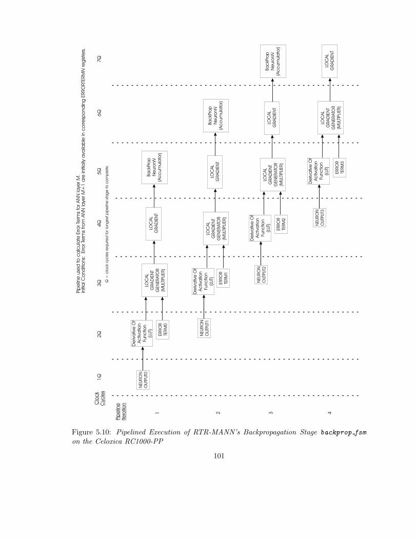
NEU
RO
N
OU
TPU
T0
De
riva
tive
Of
Ac
tiva
tion
Func
tion
(LU
T)LO
CA
L
GRA
DIE
NT
Pip
elin
e
Ite
ratio
nClo
ck
Cyc
les
1Q
2Q
3Q
4Q
5Q
6Q
7Q
1 2 3 4
Q =
clo
ck
cyc
les
req
uire
d fo
r lo
ng
est
pip
elin
e s
tag
e to
co
mp
lete
.
Pip
elin
e u
sed
to
ca
lcula
te E
rro
r Te
rms
for A
NN
laye
r.
MIn
itia
l Co
nd
itio
ns:
Erro
r Te
rms
fro
m A
NN
laye
r+
1 a
re in
itia
lly a
va
ilab
le in
co
rre
spo
nd
ing
ERRO
RTE
RM
reg
iste
rs.
MN
ERRO
R
TERM
0
LOC
AL
GRA
DIE
NT
GEN
ERATO
R
(MU
LTIP
LIER)
Ba
ckP
rop
Ne
uro
n
(Ac
cum
ula
tor)
N
NEU
RO
N
OU
TPU
T1
De
riva
tive
Of
Ac
tiva
tion
Func
tion
(LU
T)LO
CA
L
GRA
DIE
NT
ERRO
R
TERM
1
LOC
AL
GRA
DIE
NT
GEN
ERATO
R
(MU
LTIP
LIER)
Ba
ckP
rop
Ne
uro
n
(Ac
cum
ula
tor)
N
NEU
RO
N
OU
TPU
T2
De
riva
tive
Of
Ac
tiva
tion
Func
tion
(LU
T)LO
CA
L
GRA
DIE
NT
ERRO
R
TERM
2
LOC
AL
GRA
DIE
NT
GEN
ERATO
R
(MU
LTIP
LIER)
NEU
RO
N
OU
TPU
T3
De
riva
tive
Of
Ac
tiva
tion
Func
tion
(LU
T)
ERRO
R
TERM
3
LOC
AL
GRA
DIE
NT
LOC
AL
GRA
DIE
NT
GEN
ERATO
R
(MU
LTIP
LIER)
Ba
ckP
rop
Ne
uro
n
(Ac
cum
ula
tor)
N
Figure 5.10: Pipelined Execution of RTR-MANN’s Backpropagation Stage backprop fsm
on the Celoxica RC1000-PP
101
for calculating the derivative of logsig(
f ′(H(s)k )
)
, since the activation function(
f(H(s)k )
)
used in RTR-MANN’s feed-forward stage is the logsig function. The derivative of logsig(
f ′(H(s)k )
)
can easily be calculated directly from its associated neuron output(
o(s)k
)
, as
shown in Equation 2.11. Each neuron output in the sth layer is pre-loaded into backrop fsm’s
’NEURON OUTPUT N’ register (where N= k), and waits its turn to be transferred as input to
the ’Derivative of Activation Function’ unit (via NeuronOutBus data bus).
The ’Derivative of Activation Function’ was implemented as a look-up table (LUT),
and has become an unofficial member of the uog fixed arith library. The LUT architec-
ture used was exactly the same as the uog logsig rom architecture, except that the table
entries were modified to resemble the derivative of logsig(
f ′(H(s)k )
)
curve.
Once the ’Derivative of Activation Function’ output(
f ′(H(s)k )
)
is ready, it is
transferred along with the associated error term(
ε(s)k
)
in parallel to the input ports of
’LOCAL GRADIENT GENERATOR’ over separate data buses (i.e. DerivativeActivationBus
and ErrorTermBus respectively).
As its name implies, the ’LOCAL GRADIENT GENERATOR’ logic unit is simply a multiplier
used to generate the local gradient(
δ(s)k
)
for the kth neuron in the sth layer, as required
by Equation 2.10. The ’LOCAL GRADIENT GENERATOR’ was implemented as an instance of
uog booth multiplier multiplier found in the area-optimized uog fixed arith library.
Even though all of backprop fsm’s ’Backprop Neurons 0...N’ in the sth layer process
a single local gradient(
δ(s)k
)
in parallel, each of the local gradients themselves are intro-
duced to this group of logic units in a sequential manner. Similarly, a single ’Derivative
of Activation Function’ and ’LOCAL GRADIENT GENERATOR’ can only mean sequential
processing of derivative of activation(
f ′(H(s)k )
)
and error term(
ε(s)k
)
respectively. Just
like ffwd fsm, all of this sequential processing in backprop fsm was accelerated through
pipelined execution. The backprop fsm datapath utilizes a 5-stage arithmetic pipeline
for calculating derivative of activation, local gradient, and error term (if hidden layer)
for all neurons in a given layer.
102

A walk-through of the first iteration of backprop fsm’s 5-stage pipeline, as shown in
Figure 5.10, is as follows (in accordance with the nomenclature used in Equations 2.9–2.10):
STAGE#1 Neuron output(
o(s+1)j
)
of the jth neuron (where j = 0) is transferred to the
’NEURON OUTPUT 0’ register.
STAGE#2 Neuron output(
o(s+1)j
)
for neuron 0 in (s + 1)th layer is transferred as input
to ’Derivative of Activation Function’, and error term(
ε(s+1)j
)
should already
have been transferred to ’ERROR TERM N’ register (where N=j).
STAGE#3 Both the ’Derivative of Activation Function’(
f ′(H(s+1)j )
)
calculated in
the previous stage of pipeline, and error term(
ε(s+1)j
)
in ’ERROR TERM N’ register
(where N= j) are transferred as input into the ’LOCAL GRADIENT GENERATOR’.
STAGE#4 Local gradient(
δ(s+1)j
)
for the jth neuron in the (s + 1)th layer is transferred
from ’LOCAL GRADIENT GENERATOR’ to ’LOCAL GRADIENT’ register.
STAGE#5 Local gradient(
δ(s+1)j
)
from ’LOCAL GRADIENT’ register is transferred into
’Backprop Neuron 0...N’ units for processing.
Re-iteration of this pipeline is done for each and every neuron in the (s + 1)th layer, where
s = 1, . . . , (M − 1).
When applied to backprop fsm’s 5-stage arithmetic pipeline, Equation 5.5 revealed
that backprop fsm can experience a speedup (Spipe) in neuron processing of up to five
times (500%) when pipelining is used15. By accelerating neuron processing, backprop fsm’s
5-stage arithmetic pipeline has helped contribute toward the goal of maximizing RTR-
MANN’s processing density.
15This maximum theoretical speedup does not account for latencies due to memory I/O operations andFPGA reconfiguration times.
103

5.5.3 Weight Update Stage (weight update fsm)
The following is a high-level description of the weight update weight update fsm stage’s
steps of execution on the Celoxica RC1000-PP:
1. Starting with the hidden layer closest to the output layer (i.e. s = (M − 1)) and
stepping backwards through the ANN one layer at a time:
• Calculate change in synaptic weight (or bias) ∆w(s+1)kj corresponding to the gra-
dient of error for connection from neuron unit j in the (s)th layer, to neuron k
in the (s+1)th layer. This calculation is done in accordance with Equation 2.12.
• Calculate the updated synaptic weight (or bias) w(s+1)kj (n + 1) to be used in the
next Feed-Forward stage, according to Equation 2.13.
Unlike RTR-MANN’s other two stage’s of operation, the weight update (wgt update fsm)
stage was not based on Eldredge’s Time Multiplexed Interconnection scheme. However,
what the weight update (wgt update fsm) stage does share in common with the other two
stage is the same external I/O interface, the logic used to interface with RC1000-PP’s on-
board memory, and utilization of area-optimized arithmetic units from uog fixed arith.
Similar to the convention used in naming RTR-MANN’s other two stages, the weight update
stage was named after its top-level control unit. The weight update stage’s control unit was
named wgt update fsm, which is an abbreviation for Weight Update Finite State Machine.
So how were the subset of equations translated into the weight update wgt update fsm
stages resulting hardware architecture? This can only be answered by taking a closer look
at the datapath controlled by wgt update fsm16, as shown in Figure 5.11. Assuming all
registers (i.e. ’NUM NEURONS N’, ’PrevLayerOut N’, ’LOCAL GRAD N’, etc.) in the datapath
have been loaded with the appropriate data from RTR-MANN’s memory map, the change in
synaptic weight(
∆w(s)kj
)
(or change in bias(
∆θ(s)k
)
) from Equation 2.12 must be calculated
first. The change in bias(
∆θ(s)k
)
or change in synaptic weight(
∆w(s)kj
)
, which conjoin the
16Consequently, the specifications for the weight update stage wgt update fsm are given in Appendix F
104

SRA
MBA
NK
0
SRA
MBA
NK
1
SRA
MBA
NK
2
SRA
MBA
NK
3
MA
RM
B1
MB2
MB3
MB4
MB5
MB6
MB7
MB0
MO
WN
MC
EM
RW Me
mo
ryC
ontro
ller
(FSM
)
LOC
AL
GRA
D0
LEA
RN
ING
RATE
Pre
vLa
yer
Outp
ut
NEW
WG
T0
NEW
WG
T1
NEW
WG
TN
WG
T_U
PD
ATE
(To
p-le
vel)
Ad
dre
ssG
ene
rato
r(L
UT)
MultlReset
RESE
T
DO
NE
laye
r_c
ounte
r
ne
uro
n_c
ounte
r
pa
tte
rn_c
ounte
r
Xilinx
Virt
ex
20
00
e F
PG
A
Ad
drG
enRe
set
Me
mC
ontR
ese
t
TOTA
L_PA
TTERN
S
TOTA
L_LA
YERS
NO
TE:
(N
+1
) =
ma
x ne
uro
ns
ina
ny
giv
en la
yer
Wg
tM
ulti
plie
r0
MA
X_N
EU
RO
N
Sca
led
Gra
dM
ult0
Wg
tM
ulti
plie
r1
Wg
tM
ulti
plie
rN
NU
M_
NEU
RO
NS0
NU
M_
NEU
RO
NS1
NU
M_
NEU
RO
NSN
WG
T0
WG
T1
WG
TN
Wg
tA
dd
er0
Wg
tA
dd
er1
Wg
tA
dd
erN
LOC
AL
GRA
D1
Sca
led
Gra
dM
ult1
LOC
AL
GRA
DN
Sca
led
Gra
dM
ultN
Pre
vLa
yer
Out0
Pre
vLa
yer
Out1
Pre
vLa
yer
OutN
Figure 5.11: RTR-MANN’s Datapath for Weight Update Stage (wgt update fsm) on theCeloxica RC1000-PP
105
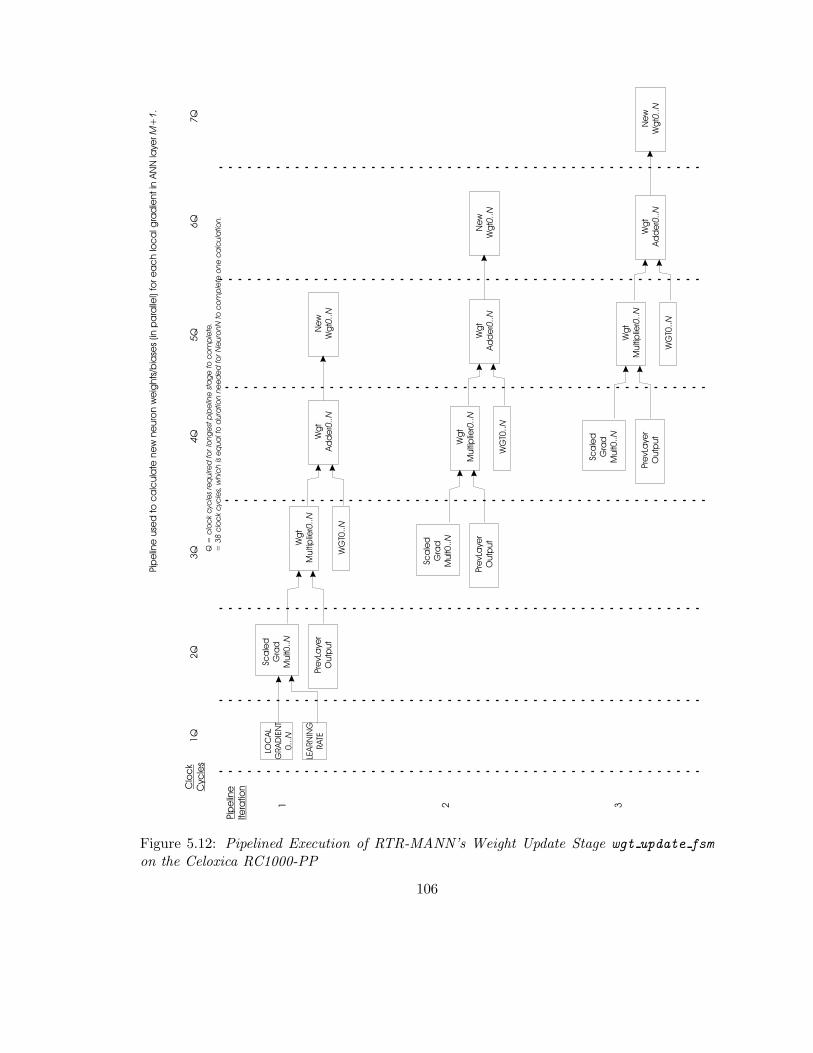
LOC
AL
GRA
DIE
NT
0..
.N
Sca
led
Gra
d
Mult0
..N
Wg
t
Multi
plie
r0..N
Pre
vLa
yer
Outp
ut
Pip
elin
e
Ite
ratio
nClo
ck
Cyc
les
1Q
2Q
3Q
4Q
5Q
6Q
7Q
1 2 3
Q =
clo
ck
cyc
les
req
uire
d fo
r lo
ng
est
pip
elin
e s
tag
e to
co
mp
lete
.
= 3
8 c
loc
k c
ycle
s, w
hic
h is
eq
ua
l to
dura
tio
n n
ee
de
d fo
r N
euro
nN
to
co
mp
lete
one
ca
lcula
tio
n.
Pip
elin
e u
sed
to
ca
lcula
te n
ew
ne
uro
n w
eig
hts
/bia
ses
(in p
ara
llel)
for e
ac
h lo
ca
l gra
die
nt in
AN
N la
yer
.M
+1
LEA
RN
ING
RATE
WG
T0..
N
Wg
t
Ad
de
r0..N
Ne
w
Wg
t0..N
Sca
led
Gra
d
Mult0
..N
Wg
t
Multi
plie
r 0..N
Pre
vLa
yer
Outp
ut
WG
T0..
N
Wg
t
Ad
de
r0..N
Ne
w
Wg
t0..N
Sca
led
Gra
d
Mult0
..N
Wg
t
Multi
plie
r 0..N
Pre
vLa
yer
Outp
ut
WG
T0..
N
Wg
t
Ad
de
r0..N
Ne
w
Wg
t0..N
Figure 5.12: Pipelined Execution of RTR-MANN’s Weight Update Stage wgt update fsm
on the Celoxica RC1000-PP
106
jth neuron in the (s − 1)th layer to kth neuron in sth layer, is calculated using the ’Scaled
Grad Mult N’ and ’Wgt Multiplier N’ logic units (where N= k). Both of these logic units
are instances of the uog booth multiplier multipliers from the uog fixed arith custom
arithmetic library. As its name implies, the ’Scaled Grad Mult N’ multiplier calculates
the scaled local gradient(
ηδ(s)k
)
, which is then used in conjunction with one of the corre-
sponding neuron output(
o(s−1)j
)
as input into ’Wgt Multiplier N’ (where N= k) to satisfy
Equation 2.12.
Next, the change in synaptic weight(
∆w(s)kj
)
that was just output by ’Wgt Multiplier
N’ (where N= k) can then be added to the corresponding synaptic weight(
w(s)kj (n)
)
to satisfy
Equation 2.13. Alternatively, if change in bias(
∆θ(s)k
)
was just output by ’Wgt Multiplier
N’ (where N= k), it can instead be added to the corresponding bias(
θ(s)k
)
to satisfy Equa-
tion 2.13. Either way, these two values are added together using the ’Wgt Adder N’ logic
unit (where N= k), which is an instance of uog std adder from the uog fixed arith arith-
metic library. Once ’Wgt Adder N’ has calculated the updated synaptic weight(
w(s)kj (n + 1)
)
(or updated bias(
θ(s)kj (n + 1)
)
), this value is written to RTR-MANN’s memory map for use
in the next iteration of the ffwd fsm stage.
Even though all of wgt update fsm’s ’Wgt Multiplier 0...N’ process a single neuron
output(
o(s−1)j
)
from the (s−1)th layer in parallel, each of the neuron output(
o(s−1)j
)
them-
selves are introduced to this group of logic units in a sequential manner. This arrangement
allows wgt update fsm to maintain the same scalability as RTR-MANN’s other two stages
of operation, which limits hardware growth of wgt update fsm to O(n) (where n is the total
number of neurons contained in the network). Fortunately, the sequential behaviour
seen wgt update fsm was accelerated by means of a 5-stage arithmetic pipeline
for calculating scaled local gradient, change in synaptic weight (or bias), and updated
synaptic weight (or bias) for all neurons in a given layer.
A walkthrough of the first iteration of wgt update fsm’s 5-stage pipeline, as shown in
Figure 5.12, is as follows:
STAGE#1 (For first iteration of pipeline only) Each local gradient(
δ(s)k
)
associated
107

with the kth neuron in the sth layer is transferred to the ’LOCAL GRADIENT k’ register
(where k = 0, . . . ,N). In parallel, the learning rate (η) is transferred to the ’LEARNING
RATE’ register.
STAGE#2 For first iteration of pipeline only, the local gradient(
δ(s)k
)
associated the kth
neuron in the sth layer, and learning rate (η) are all simultaneously transferred as
input into ’Scaled Grad k’ (where k = 0, . . . ,N). For every iteration of the pipeline,
the jth neuron output(
o(s−1)j
)
(where j = 0) in the (s − 1)th layer is loaded into its
respective ’PrevLayerOutput k’ registers (where k = 0, . . . ,N).
STAGE#3 In order to determine change in synaptic weight(
∆w(s)kj
)
, the scaled local
gradient(
ηδ(s)k
)
, and associated neuron output(
o(s−1)j
)
are transferred as input into
’Wgt Multiplier k’ (where k = 0, . . . ,N), whereas the value 1.0 is substituted for
neuron output if calculating the change in bias(
∆θ(s)k
)
instead. Depending on what’s
being calculated, either the synaptic weight(
w(s)kj (n)
)
or bias(
θ(s)k (n)
)
is transferred
into a respective ’WGT k’ register (where k = 0, . . . ,N).
STAGE#4 For calculating updated synaptic weight(
w(s)kj (n + 1)
)
, the change in synaptic
weight(
∆w(s)kj (n)
)
and current synaptic weight(
w(s)kj (n)
)
are transferred from ’Wgt
Multiplier k’ and ’Wgt k’ respectively, to ’Wgt Adder k’ (where k = 0, . . . ,N) in par-
allel. For calculating updated bias(
θ(s)k (n + 1)
)
, the change in bias(
∆θ(s)k (n)
)
and
current bias(
θ(s)k (n)
)
are transferred from ’Wgt Multiplier k’ and ’Wgt k’ respec-
tively, to ’Wgt Adder k’ (where k = 0, . . . ,N) in parallel.
STAGE#5 The output of ’Wgt Adder k’, whether it be either an updated synaptic weight(
w(s)kj (n + 1)
)
or updated bias(
θ(s)k (n + 1)
)
, is transferred to ’New Wgt k’ register
(where k = 0, . . . ,N), and waits to be stored in RTR-MANN’s memory map.
Re-iteration of this pipeline is done until all neuron weights (and biases) in the sth layer
have been calculated (where s = 1, . . . ,M).
Despite a two-stage delay before the 2nd iteration of wgt update fsm’s 5-stage pipeline
begins, Equation 5.5 can still be used to determine that maximum theoretical speedup
108
(Spipe) can still be applied. As a result, it turned out wgt update fsm can experience a
speedup (Spipe) in neuron weight / bias updates of up to five times (500%) when pipelining
is used17 By accelerating the rate of neuron weight / bias updates, wgt update fsm’s 5-stage
arithmetic pipeline has helped contribute toward the goal of maximizing RTR-MANN’s
processing density. Lastly, it should be noted that modelling the entire wgt update fsm
in SystemC presented no real challenges, which is due in part to the lessons learned and
practical experience that had been gained in modelling RTR-MANN’s previous two stages
in SystemC.
5.5.4 Summary
This section has explained how the Backpropagation Algorithm equations (originally pre-
sented in Section 2.4) were divvied up among RTR-MANN’s three stages of operation and
translated into hardware using uog fixed arith arithmetic library. Some sequential exe-
cution had to be tolerated in all three of RTR-MANN’s stages of operation in order to limit
hardware growth to O(n) (where n is equal to the total number of neurons contained in
the network), thereby allowing the architecture to easily scale up to any size ANN topol-
ogy being tested. Fortunately, RTR-MANN was able to use arithmetic pipelines in each
of its three stages of operation, which was shown to accelerate sequential execution up to
four or five times (400%–500%), thereby increasing the overall processing density of this
architecture.
Some challenges were faced when modelling RTR-MANN entirely in SystemC. The lim-
ited capacity of SystemC’s memory stack made it impossible to model any of RTR-MANN’s
logic units using large array declarations in SystemC. As a result, LUT functionality
in the uog fixed arith library (i.e. uog logsig rom and ’Derivative of Activation
Function’) had to be emulated in SystemC using C/C++ math functions, rather than
modelling LUTs using SystemC array declarations. Taking a behavioural design approach
17The maximum theoretical speedup does not account for latencies due to memory I/O operations andFPGA reconfiguration times.
109
such as this was acceptable for simulation purposes. However, a structural design approach
using SystemC array declarations would have been more preferable, since it offers a more
accurate representation of LUTs in hardware. The next section will give a performance
evaluation of the RTR-MANN architecture, where SystemC behavioural simulations were
carried out for several different ANN application examples.
5.6 Performance Evaluation of RTR-MANN
This section will quantify the performance of RTR-MANN, in addition to the benefits gained
in using a systems design methodology (via SystemC HLL). The following three studies used
to evaluate the performance of RTR-MANN will be covered:
Performance using a simple ’toy’ problem - where RTR-MANN will be used to solve
the classic logical-XOR problem.
Performance using a more complex real-world problem - where RTR-MANN will
be used to solve the classic Iris problem.
Quantification of RTR-MANN’s processing density - where RTR-MANN’s recon-
figurable computing performance will be quantified using Wirthlin’s functional density
metric. RTR-MANN will then be compared to Eldredge’s RRANN architecture ac-
cording to their respective processing densities.
Ultimately, RTR-MANN’s performance evaluation is benchmark of how well the recent
improvement in tools and methodologies used have strengthened reconfigurable computing
as a platform for accelerating ANN testing.
5.6.1 Logical-XOR example
RTR-MANN’s architecture was initially proved out (i.e. verified / validated) using a sim-
ple ANN application; the classic logical-XOR problem. The exact same initial topology
110

parameters and thirty trials of training data originally generated for the Non-RTR ANN
implementation to solve the logical-XOR problem in Chapter 4 were re-applied to the RTR-
MANN architecture. Each training session lasted either a length of 5000 epochs, or until
RTR-MANN successfully converged (i.e. < 10% error) to solve the logical-XOR problem,
which ever came first. Similar to the Non-RTR ANN implementation in Chapter 4, RTR-
MANN is limited to sequential (pattern-by-pattern) training only, and does not currently
support batch training.
All training sessions were simulated using the SystemC model of RTR-MANN, which
was carried out on a PC workstation running Windows 2000 operating system, with 512MB
of memory and an Intel P4 1.6GHz CPU. Development was also carried out on the same
PC workstation, where each stage of RTR-MANN’s SystemC model was created using MS
Visual C++ v6.0 IDE and SystemC v2.0.1 class library. ActiveState ActiveTcl 8.4.1.0 was
required for the simulations to run, since a Tcl script was used to automate sequential exe-
cution of the SystemC binary software program; once for each RTR-MANN stage. The Tcl
script also guaranteed that training occurred for the correct number of epochs, as specified
by the user. To ensure semantic correctness, the output of each of RTR-MANN’s logic
units were manually calculated in a spreadsheet and compared to the actual output ob-
served during it’s first few logical-XOR ANN training sessions18. SystemC’s native support
for displaying fixed-point datatypes in a real number format made it extremely easy to
interpret RTR-MANN’s output during simulation.
Not only was RTR-MANN found to be semantically correct, but all thirty
training sessions of the logical-XOR problem successfully converged (i.e. 100%
convergence) for this architecture. It only took four hours to run one trial of
5000 epochs using the SystemC model of RTR-MANN. It’s no surprise that just
like the 16-bit Non-RTR ANN implementation of Chapter 4, RTR-MANN converged for all
thirty trials of the logical-XOR training data. Not only are both architectures were based
on uog fixed arith library, but they were both given the same initial topology parameters
18Manual validation was only done for the first few iterations of the backpropagation algorithm.
111
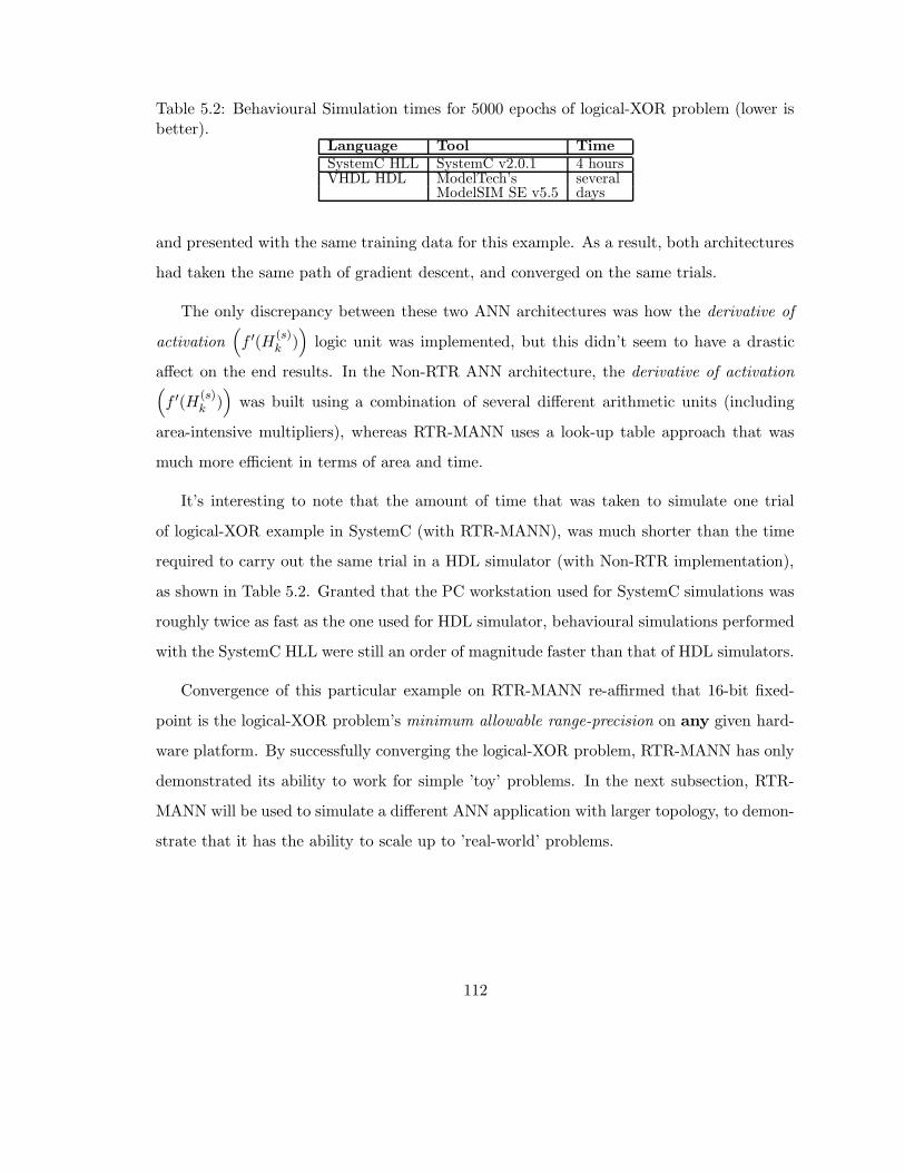
Table 5.2: Behavioural Simulation times for 5000 epochs of logical-XOR problem (lower isbetter).
Language Tool TimeSystemC HLL SystemC v2.0.1 4 hoursVHDL HDL ModelTech’s several
ModelSIM SE v5.5 days
and presented with the same training data for this example. As a result, both architectures
had taken the same path of gradient descent, and converged on the same trials.
The only discrepancy between these two ANN architectures was how the derivative of
activation(
f ′(H(s)k )
)
logic unit was implemented, but this didn’t seem to have a drastic
affect on the end results. In the Non-RTR ANN architecture, the derivative of activation(
f ′(H(s)k )
)
was built using a combination of several different arithmetic units (including
area-intensive multipliers), whereas RTR-MANN uses a look-up table approach that was
much more efficient in terms of area and time.
It’s interesting to note that the amount of time that was taken to simulate one trial
of logical-XOR example in SystemC (with RTR-MANN), was much shorter than the time
required to carry out the same trial in a HDL simulator (with Non-RTR implementation),
as shown in Table 5.2. Granted that the PC workstation used for SystemC simulations was
roughly twice as fast as the one used for HDL simulator, behavioural simulations performed
with the SystemC HLL were still an order of magnitude faster than that of HDL simulators.
Convergence of this particular example on RTR-MANN re-affirmed that 16-bit fixed-
point is the logical-XOR problem’s minimum allowable range-precision on any given hard-
ware platform. By successfully converging the logical-XOR problem, RTR-MANN has only
demonstrated its ability to work for simple ’toy’ problems. In the next subsection, RTR-
MANN will be used to simulate a different ANN application with larger topology, to demon-
strate that it has the ability to scale up to ’real-world’ problems.
112

5.6.2 Iris example
Fisher’s Iris problem [19] is a classic in the field of pattern recognition, and is referenced
frequently to this day ([14], pg. 218). The dataset for this problem contains three classes
of 50 instances (i.e. 150 instances in total), where each class refers to a specific type of Iris
plant:
• Iris Setosa
• Iris Versicolour
• Iris Virginica
Given an Iris plant whose type is unknown, the following four unique features can be used
to distinguish its type:
• septal length in cm
• septal width in cm
• petal length in cm
• petal width in cm
One Iris class is linearly separable from the other two, but the latter are not linearly
separable from each other. Hence, Fisher’s Iris dataset is a non-linear separable problem,
which was used to demonstrate RTR-MANN’s ability to solve a typical ’real-world’ example.
The ANN topology required to solve the Iris problem was dependent on its data set.
The number of neuron inputs was equal to the number of Iris features, whereas the number
of neurons in the output layer was equal to the number of classes (i.e. Iris plant types).
Like most ANN applications, at least one hidden layer was required in the topology to
solve this non-linear separable problem, the size of which had to be determined through
experimentation. As a result, a 4–x–3 topology was used (where x = number of neurons
113

in hidden layer). RTR-MANN’s goal was to classify the input, and assign a value of ’1’ to
the output neuron that corresponded to the correct class of Iris plant (whereas all other
neurons in the output layer would be assigned a value of ’0’).
5.6.2.1 Ideal ANN Simulations in Matlab
A Matlab script was first used to determine the ideal19 solution space required for a fully-
connected backprop ANN (with 3–x–4 topology) to successfully converge on the Iris data
set. Once this was established, the Matlab script, called iris3 incremental.m, would then
be used to generate initial topology parameters, which were known to successfully converge
the Iris data set. As a means of verification / validation, RTR-MANN’s architecture could
then be trained using these same sets of initial parameters to see if it would be able to
re-produce this expected behaviour in simulation.
The Matlab script determined the Iris data set’s solution space using the following
topology parameters:
• Only 4–2–3 and 4–3–3 fully-connected topologies were used.
• Neuron inputs were normalized to [0, 1] since the logsig function was used as the
activation function.
• Only the first 100 patterns from the Iris data set were used for training, whereas the
remaining 50 patterns were used for testing.
• Initial neuron weights / biases used were randomly generated between [−1, 1].
• Learning Rates used were 0.1, 1, 2, 5, and 8.
• Training goal was to converge to a mean squared error ≤ 0.10.
• Sequential (pattern-by-pattern) training was used.
19An ideal solution space for ANNs corresponds to one determined using 32-bit floating-point calculations(as opposed to a non-ideal case where fixed-point calculations are used.
114
The PC workstation used to carry out these Matlab ANN simulations, plus the RTR-
MANN Iris training that was conducted shortly thereafter, was the same environment that
had been previously used for RTR-MANN’s logical-XOR example. In addition, MATLAB
v6.5.0 (Release 13) and the Matlab Neural Network Toolbox v4.0 were both required to run
the iris3 incremental.m Matlab script. The following observations were noted when the
Iris ANN simulations were conducted in Matlab:
1. ANN converged to a correct solution using all combinations of topology parameters
tested.
2. Convergence for all simulations occurred in under 1500 epochs of training.
3. As the network started to converge, change in synaptic weight (or bias)(
∆w(s+1)kj
)
observed had magnitudes of 10−5 when a learning rate (η) = 0.1 was used, whereas a
magnitude of 10−4 was seen for learning rates (η) = 1, 2, 5, and 8.
4. During and after training, neuron weights / biases had values within a range of
[−4.25, 3.0]
These observations helped predict some sources of error (i.e. noise factors) in RTR-MANN,
which may result should it use the same combinations of ANN topology parameters in its
own training to solve the Iris problem.
1. Change in synaptic weight (or bias)(
∆w(s+1)kj
)
of magnitude 10−5 for learning rate
(η) = 0.1 in Matlab would result in change in synaptic weight (or bias)(
∆w(s+1)kj
)
= 0 for RTR-MANN. Unfortunately, RTR-MANN range-precision can only represent
values as small as 2−12 � 10−5. Hence, learning rates of magnitude 10−1 were never
tested with RTR-MANN since small weight updates would have been set to zero and
no learning would have taken place. Instead, RTR-MANN used only learning rates of
magnitude 100, where chances of underflow were less likely to occur.
2. Hardware overflow may occur in RTR-MANN’s weighted sum(
H(s)k
)
calculations for
any layers having two or more neurons. With weights / biases of range [-4.25,3.0]
115
and neuron outputs of range [0, 1.0], a layer with two neurons could produce weight
weighted sum(
H(s)k
)
with range [-12.75, 9.0] (according to Equation 2.6), whereas
RTR-MANN only supports a range of [−8.0, 8.0) Errors due to overflow would cause
the ANN to deviate away from its intended path of gradient descent in weight error
space. Such behaviour could result in slower convergence rates or no convergence at
all.
These two issues cause a paradox in the choice of range-precision used by RTR-MANN to
solve the Iris problem. Increasing precision to 2−14 would allow RTR-MANN to represent
numbers of magnitude 10−5 to prevent underflow from occurring, but would further reduce
the range in a 16-bit fixed-point representation down to [−2, 2). Similarly, increasing range
to prevent overflow errors would only further limit the precision. In any case, this paradox
suggests that RTR-MANN may lack the range-precision needed to successfully converge the
Iris data set without compromise. RTR-MANN simulations of the Iris example were run to
see how these predicted noise factors affected convergence rates.
5.6.2.2 RTR-MANN Simulations w/o Gamma Function
The RTR-MANN SystemC model was setup using initial parameters that were known to
solve the Iris problem in Matlab. Three separate trials20 were run in total, where RTR-
MANN used a 4–3–3 topology and a learning rate of 1.0. In order to comply with the
Matlab ANN model, RTR-MANN’s weight update(
wskj(n + 1)
)
had to be negated, as
shown in Equation 5.6, for all Iris training sessions. To ensure semantic correctness of
RTR-MANN, manual verification was done in addition to SystemC simulations, just as it
had been previously done for RTR-MANN’s logical-XOR example.
wskj(n + 1) = ∆w
(s)kj (n) − w
(s)kj (n) (5.6)
20Also referred to as Iris Trial#1, #2, and #3.
116
, where nomenclature used is same as described in Equation 2.13
Although RTR-MANN was found to be semantically correct, the SystemC model did
not converge to the ’correct’ solution. In all three trials, RTR-MANN had converged after
only 10 epochs, where neuron errors(
ε(s)k
)
in the output layer were observed to have
values of either ±2−12, or ±(1 − 2−12)). When these values were used in combination with
neuron output(
o(s)k
)
values of same magnitude, all remaining neuron error (and hence,
local gradient) calculations had underflow to a value of zero, and no learning took place. It
should also be noted that it took six hours for RTR-MANN’s SystemC model to simulate
200 epochs of Iris training. Compared to the SystemC simulation of logical-XOR problem,
Iris training sessions took substantially longer due to bigger topology and more training
data used.
The fact that the RTR-MANN 16-bit platform failed to converge using initial parameters
that were known to converge for its 32-bit floating-point equivalent in Matlab showed that
16-bit fixed-point is NOT the minimum allowable range-precision of every backpropagation
application. Further review of Holt and Baker’s [22] research confirmed that 16-bit range-
precision was, in fact, not sufficient for hardware ANNs to learn ’real-world’ problems. Holt
and Baker have previously introduced special mechanisms to improve performance lost due
to lack of range-precision, which is re-cited as follows [22]:
Slight deviations from standard backpropagation are used on a few of the prob-
lems as noted. These include:
1. Gamma Function: A small offset factor, γ, is added to the derivative of the
sigmoid to prevent nodes from becoming stuck on the tails of the sigmoide
where the derivative is zero. This change improves the rate of convergence
for both the integer [i.e. fixed-point] and the floating-point simulators.
2. Marginal Function: In training, if the error at the output of a neuron is less
than a specified margin, then the error is set to zero and no learning takes
117

place. A small margin is reported in many of the papers on backpropagation
training and sometimes help a network converge.
It seems as though RTR-MANN’s Iris training suffers from the same problems documented
by Holt and Baker, in addition to risk of overflow errors which may have occurred in
weighted sum(
H(s)k
)
calculations. Initial results have made it clear that RTR-MANN by
itself cannot learn the Iris example due to noise factors (i.e. errors), which resulted from
the lack of range-precision required for this problem.
5.6.2.3 RTR-MANN Simulations with Gamma Function
A Gamma Function, γ, was introduced into RTR-MANN’s architecture as a second attempt
at trying to solve the Iris problem. The Gamma Function (γ) is simply an offset which is
added to the derivative of activation function(
f ′(H(s)k )
)
, as shown in Equation 5.7.
f ′(H(s)k )gamma = f ′(H
(s)k ) + γ = os
k(1 − osk) + γ for logsig function (5.7)
Five more trials were generated by Matlab, each of which consist of a set of initial topology
parameters known to successfully converge the Iris problem. Each of these five trials were
then applied to RTR-MANN with Gamma Function (γ) enabled, and are referred to as Iris
Trial #4 thru #8.
Iris Trial #4 demonstrates the impact the Gamma Function (γ) made on RTR-MANN’s
performance, as shown in Table 5.3. When γ = 0, no gamma function was present and the
network stopped learning after just ten epochs of training. Table 5.3 reveals that no matter
how many epochs were ran, RTR-MANN with γ = 0 only ever converged on 16% of the Iris
test data21.
With γ = 0.01, RTR-MANN’s output layer was able to continuously learn. However, as
the network started to converge and error term(
ε(s)k
)
got smaller, all error credit assignment
21This test result corresponds to 8 out of 50 Iris test patterns with output error“
ε(s)k
”
less than or equal
to ±0.022460937500.
118

Table 5.3: RTR-MANN convergence for Iris ExampleEpochs Trial#4
0 0/50 (0%) 0/50 (0%) 0/50 (0%)10 8/50 (16%) N/A N/A200 8/50 (16%) 11/50 (22%) 44/50 (88%)400 8/50 (16%) 14/50 (28%) 36/50 (72%)600 8/50 (16%) 29/50 (58%) 0/50 (0%)800 8/50 (16%) 9/50 (18%) 41/50 (91%)1000 8/50 (16%) 7/50 (14%) 34/50 (68%)1200 8/50 (16%) 6/50 (12%) N/A
GammaFunction 0.0 0.01 0.10
Table 5.4: Repeatability of RTR-MANN convergence for Iris exampleEpochs Trial#5 Trial#6 Trial#7 Trial#8
0 0/50 (0%) 0/50 (0%) 0/50 (0%) 0/50 (0%)50 N/A N/A 35/50 (70%) N/A100 N/A 38/50 (76%) 26/50 (52%) N/A150 N/A 43/50 (86%) 23/50 (46%) N/A200 43/50 (86%) 26/50 (52%) 15/50 (30%) 44/50 (88%)
GammaFunction 0.10 0.10 0.10 0.10
propagated back to the hidden later was too small, and no learning took place. So while
the output layer continued to learn, the hidden layer did not, which caused the ANN’s path
of gradient descent to deviate from the intended path. Table 5.3 shows that this occurred
after about 600 epochs, where convergence peaked at 58%. Although γ = 0.01 did improve
RTR-MANN’s convergence for Iris Trial#4, it was not sufficient enough to be considered a
successful convergence.
With γ = 0.10, both hidden and output layers continued learning no matter how small
the error terms(
ε(s)k
)
got as the network converged. Table 5.3 reveals that for γ = 0.1,
convergence percentages started to fluctuate once the RTR-MANN successfully converged
at 200 epochs. This is due to the fact that γ = 0.10 forces RTR-MANN to continue
learning even after it has converged; after the path of gradient descent has made its way
to some local / global minimum in the neuron weight’s error space. The Gamma Function
introduced weight changes that were significant enough to cause the path of gradient descent
to then jump out of local / global minimum onto a nearby hill of a local / global maximum.
RTR-MANN would then start to search for another local / global minimum thereafter, and
119
so on and so forth. Note that such behaviour is commonly seen in any backpropagation
ANN which continues to learn once it has successfully achieved convergence. In RTR-
MANN’s case, this behaviour may have been amplified by its’ noise factors. Nonetheless,
these observations show that RTR-MANN was finally able to successfully converge on Iris
Trial#4 (when a value of γ = 0.10 was used). Iris Trial#5 thru #8 in Table 5.4 were
run simply to demonstrate that the success of Iris Trial#4 wasn’t an isolated case, and
that RTR-MANN could repeat this kind of performance for different sets of initial topology
parameters.
In summary, convergence of the Iris example could only be achieved when a Gamma
Function (γ) was employed. This confirms that 16-bit fixed-point is below the minimum al-
lowable range-precision required for the Iris problem to guarantee same convergence rates as
a 32-bit floating-point platform. This also confirms that minimum allowable range-precision
is application dependent, which must be determined empirically. In this subsection, the key
to determining minimum allowable range-precision empirically was to first build an ideal
ANN model for the application, then observe the maximum numerical range seen in weighted
sum(
H(s)k
)
calculations and minimum numerical precision seen in change in synaptic weight(
∆w(s)kj (n)
)
as the error term gets ever smaller until successful convergence occurs. For the
Iris problem, such observations suggested that 24-bit fixed-point (1 sign bit, 4 bits for in-
teger part, and 19 bits for fraction part, which allows for range [−16, 16) and precision of
10−6) is its’ minimum allowable range-precision that would allow RTR-MANN to converge
without having to use a Gamma Function (γ). With the help of the Gamma Function (γ),
RTR-MANN has demonstrated its ability to work for the Iris problem, and hence, its ability
to scale up to ’real-world’ problems. Now that RTR-MANN’s performance in terms of ANN
simulation has been verified / validated, the next subsection will quantify its’ performance
in terms of reconfigurable computing.
120

5.6.3 RTR-MANN Density Enhancement
This section will quantify RTR-MANN’s reconfigurable computing performance by means
of Wirthlin’s functional density metric. The objective is to show how the recent maturity
in FPGA technology, tools, and related methodologies have helped improve performance in
reconfigurable computing platforms. This will be accomplished by comparing the density
enhancement (if any) of RTR-MANN relative to Eldredge’s RRANN architecture. The other
objective is to justify the reconfigurable computing approach of RTR-MANN itself. This
will be accomplished by comparing the functional density of RTR-MANN with run-time
reconfiguration employed versus a static (i.e. non-RTR) version of RTR-MANN.
Wirthlin [51] had previously quantified RRANN’s functional density, as shown in Equa-
tion 5.8, in an application whose topology required a maximum of 60 neurons per layer.
This metric was measured in terms of weight updates per second per configurable
logic block (WUPS/CLB). However, as discussed in Appendix A, the size of a CLB
varies from one FPGA family to the next. Instead, logic gates are a more suitable, more
atomic measurement of area that should be used when comparing platforms from different
FPGA families. Based upon Xilinx XC3090 specifications [55], the functional density for
RRANN was recalculated in terms of logic gates, as shown in Equation 5.9. All that re-
mained was the derivation of RTR-MANN’s functional density of RTR-MANN, before the
reconfigurable computing performance of these two architectures could be compared.
Drtr(RRANN) = 2079
(
WUPS
CLB
)
(5.8)
= 2079 ×
(
320 CLB
6000 logic gate
)
= 110.88
(
WUPS
logic gate
)
(5.9)
Keeping in mind that RTR-MANN supports a fully-connected N×N matrix of neurons,
the theoretical22 functional density of its run-time reconfigurable architecture is shown as
follows:
22Actual calculation of RTR-MANN’s functional density remains to be seen, since it has yet to be synthe-sized on RC1000-PP FPGA platform.
121

Drtr(RTR-MANN) = WUPSArea
=N2M
M [Tpipe(FFWD) + Tpipe(BACKPROP ) + Tpipe(WGTUP )] A(5.10)
,where
N = maximum number of neurons supported per layer
M = total number of layers supported
Tpipe(FFWD) = Total time (per layer) needed to complete pipeline execution of ffwd fsm
Tpipe(BACKPROP ) = Total time (per layer) needed to complete pipeline execution of
backprop fsm
Tpipe(WGTUP ) = Total time (per layer) needed to complete pipeline execution of wgt update fsm
A = Area of FPGA platform
Based on nomenclature from Equation 5.4, pipelined execution time in ffwd fsm can be
determined as follows:
Tpipe(FFWD) = mP + (n − 1)P
= (N + 3)(95 × 10−9) (5.11)
, since
m = 4 = number of stages in ffwd fsm arithmetic pipeline
P = 38400×106 because 38 clock cycles of execution time per pipelined stage, and Celoxica
RC1000-PP has a maximum clock speed of 400MHz [28]
n = N = maximum number of neurons supported per layer
122
Similarly, the pipelined execution time in backprop fsm can be determined as follows:
Tpipe(BACKPROP ) = mP + (n − 1)P
= (N + 4)(95 × 10−9) (5.12)
, since all parameters are the same as was used in Equation 5.11, except that m = 5 for back-
prop fsm. The irregular 2-stage delay in the initial iteration of the wgt update fsm pipeline
requires a modified version Equation 5.4, in order to calculate its pipelined execution time:
Tpipe(WGTUP ) = (m + 2)P + (n − 2)P
= (N + 4)(95 × 10−9) (5.13)
, since all parameters are the same as was used in Equation 5.11, where m = 4 for
wgt update fsm. In addition, the area (A) used for RTR-MANN is the maximum typical
gate count for the Xilinx Virtex-E XCV2000E FPGA [57], which is as follows:
A = (80 × 120 CLBs) = 2541952 logic gates (5.14)
Hence, substituting Equations 5.11 thru 5.14 back into Equation 5.10, the result is:
Drtr(RTR-MANN) =N2
(3N + 11)(95 × 10−9)(80 × 120 CLBs)(5.15)
=N2
(3N + 11)(95 × 10−9)(2541952 logic gates)(5.16)
Use of Equation 5.15 or 5.16 made it possible to calculate the theoretical functional
density of RTR-MANN for comparison with RRANN, using the assumption that a maximum
of sixty neurons was supported per layer (i.e. N = 60). Results of RTR-MANN functional
density calculations were compared to Eldredge’s RRANN architecture, as summarized in
Table 5.5. Looking at functional density in units of(
WUPSCLB
)
only, results showed that
RTR-MANN has 10x more functional density compared to that of RRANN. Although in
123
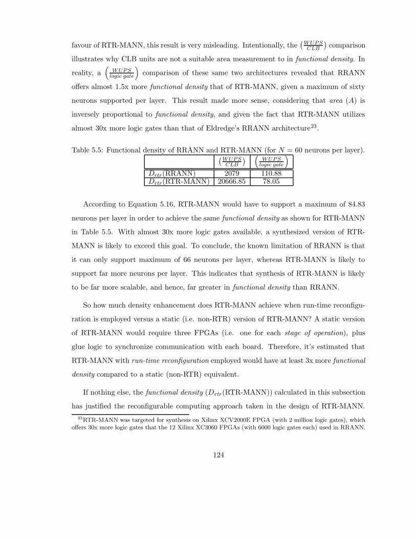
favour of RTR-MANN, this result is very misleading. Intentionally, the(
WUPSCLB
)
comparison
illustrates why CLB units are not a suitable area measurement to in functional density. In
reality, a(
WUPSlogic gate
)
comparison of these same two architectures revealed that RRANN
offers almost 1.5x more functional density that of RTR-MANN, given a maximum of sixty
neurons supported per layer. This result made more sense, considering that area (A) is
inversely proportional to functional density, and given the fact that RTR-MANN utilizes
almost 30x more logic gates than that of Eldredge’s RRANN architecture23.
Table 5.5: Functional density of RRANN and RTR-MANN (for N = 60 neurons per layer).(
WUPSCLB
)
(
WUPSlogic gate
)
Drtr(RRANN) 2079 110.88Drtr(RTR-MANN) 20666.85 78.05
According to Equation 5.16, RTR-MANN would have to support a maximum of 84.83
neurons per layer in order to achieve the same functional density as shown for RTR-MANN
in Table 5.5. With almost 30x more logic gates available, a synthesized version of RTR-
MANN is likely to exceed this goal. To conclude, the known limitation of RRANN is that
it can only support maximum of 66 neurons per layer, whereas RTR-MANN is likely to
support far more neurons per layer. This indicates that synthesis of RTR-MANN is likely
to be far more scalable, and hence, far greater in functional density than RRANN.
So how much density enhancement does RTR-MANN achieve when run-time reconfigu-
ration is employed versus a static (i.e. non-RTR) version of RTR-MANN? A static version
of RTR-MANN would require three FPGAs (i.e. one for each stage of operation), plus
glue logic to synchronize communication with each board. Therefore, it’s estimated that
RTR-MANN with run-time reconfiguration employed would have at least 3x more functional
density compared to a static (non-RTR) equivalent.
If nothing else, the functional density (Drtr(RTR-MANN)) calculated in this subsection
has justified the reconfigurable computing approach taken in the design of RTR-MANN.
23RTR-MANN was targeted for synthesis on Xilinx XCV2000E FPGA (with 2 million logic gates), whichoffers 30x more logic gates that the 12 Xilinx XC3060 FPGAs (with 6000 logic gates each) used in RRANN.
124

Should a synthesized version of RTR-MANN on RC1000-PP platform be able to support
more than 84.83 neurons, it will have more functional density and scalability than Eldredge’s
RRANN architecture. RTR-MANN is likely to far exceed this, which is due in part by
the increased logic densities seen in current-generation FPGAs, and better optimization
capabilities seen in associated synthesis tools.
It should be made clear that the functional density metric derived for RTR-MANN in
this subsection is purely theoretical. Calculation of actual functional density is easy enough
to do once RTR-MANN has been synthesized on a real platform (e.g. RC1000-PP). Only
then will the maximum number of neurons (and hence, weight updates) that RTR-MANN
can support be truly known, in addition to the actual FPGA area requirements of each
reconfigurable stage as determined by EDA synthesis tools. A benchmark of actual time
required for the real platform to complete execution of a given ANN application would
provide the last piece of information needed to calculate the actual functional density. The
original and best example of how to go about determining the actual functional density of a
synthesized ANN architecture is provided by Wirthlin [51], in his empirical determination
of this metric for Eldredge’s RRANN architecture.
5.6.4 Summary
This section has shown how RTR-MANN has benefited from using a systems design method-
ology (via SystemC HLL). As expected, the behavioural simulation rates of RTR-MANN
in SystemC were an order of magnitude faster compared to that of HDL simulators. In
addition, SystemC’s native support for displaying fixed-point datatypes in a real number
format made it extremely easy to interpret RTR-MANN’s output during simulation. The
combination of these two benefits lead to a much quicker verification / validation phase of
RTR-MANN’s system design, compared to past experiences with HDL simulators.
The following was concluded for each of the three studies used to evaluate the perfor-
mance of RTR-MANN:
125

Performance using a simple ’toy’ problem - RTR-MANN was able to solve the clas-
sic logical-XOR problem, which proved that this architecture is capable of solving
’toy’ problems.
Performance using a more complex problem - RTR-MANN by itself was not capable
of solving the classic Iris problem due to errors caused by lack of range-precision. Using
ideal ANN simulations in Matlab, a new method of empirically determining minimum
allowable range-precision was proposed, which suggested that 24-bit fixed-point would
have been sufficient for RTR-MANN to solve the Iris problem. Alternatively, RTR-
MANN’s 16-bit platform was able to successfully solve the Iris problem once a Gamma
Function (γ = 0.10) was added to the architecture. Repeatability of RTR-MANN’s
performance with Gamma Function (γ) employed was demonstrated multiple times,
where a different set of initial parameters were used in each. This proved that with the
help of a Gamma Function, RTR-MANN is capable of solving real-world problems.
Quantification of RTR-MANN’s processing density - Calculation of RTR-MANN’s
theoretical functional density helped determine that this architecture needs to support
at least 85 neurons per layer to achieve a density enhancement over Eldredge’s RRANN
architecture. RRANN can support a maximum of 66 neurons per layer, and RTR-
MANN is 30x the size of RRANN. This suggests that RTR-MANN exceeds RRANN
in both scalability and functional density. These merits are due in part by current-
generation FPGA densities and mature EDA tools used to develop RTR-MANN,
which have much improved since the creation of RRANN almost ten years ago.
5.7 Conclusions
RTR-MANN is an FPGA-based ANN architecture that has been designed from the begin-
ning to support user-defined topologies without the need for re-synthesis. The flexibility
and scalability required to do so has been made possible through the use of Eldredge’s time-
multiplexed algorithm, and RTR-MANN’s dynamic memory map. By successfully solving
126
the classic logical-XOR and Iris problems, this architecture has demonstrated how trainers
can easily define and test fully-connected ANN topologies of any size. However, the only
stipulation is that RTR-MANN must use a Gamma Function (γ) in order to scale up to
’real-world’ problems.
The hypothesis that 16-bit fixed-point would be sufficient enough to guarantee conver-
gence for all backpropagation applications turned out to be false, proving that minimum
allowable range-precision is application dependent. For example, RTR-MANN simulations
(without Gamma Function) proved that logical-XOR problem could be solved using a mini-
mum allowable range-precision of 16-bit fixed-point, whereas 24-bit fixed-point should have
been used for the Iris problem. Fortunately, this chapter has proposed a method that can
be used to empirically determine the minimum allowable range-precision of any backprop-
agation application.
A number of factors have allowed RTR-MANN to maximize its processing density, which
is the ultimate goal of reconfigurable computing:
• Run-time reconfiguration was utilized in executing each of RTR-MANN’s stages of
operation (i.e. feed-forward, backpropagation, and weight update), which is estimated
to have increased processing density by at least 3x compared to its static (i.e. non-
RTR) equivalent.
• The uog fixed arith custom 16-bit fixed-point arithmetic library was used, which is
area-optimized for RTR-MANN’s targeted platform.
• Each stage of operation employs an arithmetic pipeline, which has accelerated execu-
tion of RTR-MANN by 300%-400%.
Quantization of processing density was done using Wirthlin’s functional density met-
ric, which helped indicate that RTR-MANN has a significant density enhancement over
Eldredge’s RRANN architecture. Hence, RTR-MANN is far more scalable than RRANN,
which can be attributed to the increase in FPGA density used. In addition, use of a sys-
127
tem design methodology (via HLL) resulted in a much quicker, more intuitive verification
/ validation phase for RTR-MANN.
In conclusion, the biggest contribution that system design methodology (via HLL) has
given to reconfigurable computing is a faster, more intuitive design phase, whereas ad-
vancements in FPGA technology / tools over the last decade have led to improvement in
the scalability and functional density of such architectures. RTR-MANN is proof of how
these recent advancements have helped strengthen the case of reconfigurable computing as
a platform for accelerating ANN testing.
128
Chapter 6
Conclusions and Future Directions
A summary will be given of the role each previous chapter has played, and the contributions
each has made towards meeting thesis objectives. This exercise will also help identify
the novel contributions this thesis has made, as a whole, to the field of reconfigurable
computing. Next, limitations of RTR-MANN will be summarized, followed up with direction
on several research problems that can be conducted in future to alleviate this architecture’s
shortcomings. Lastly, some final words will be given on what advancements to expect in
next-generation FPGA technology, tools, and methodologies, and the impact it may have
on the future of reconfigurable computing.
The role of Chapter 1 was nothing more than an explanation of the motivation behind
thesis objectives; to determine the degree to which reconfigurable computing has benefited
from recent improvements in the state of FPGA technology / tools. This translated into the
case study of a newly proposed FPGA-based ANN architecture, which was used to demon-
strate how recent advancements of the tools / methodologies used have helped strengthened
reconfigurable computing as a means of accelerating ANN testing. Chapter 1 made no real
contributions towards meeting thesis objectives, other to define them.
Chapter 2 gave a thorough review of the fields of study involved in this thesis, including
reconfigurable computing, FPGAs (Field Programmable Gate Arrays), and the backpropa-
129

gation algorithm. It did nothing more than provide the necessary background required for
the reader to understand all topics covered in this thesis.
The role of Chapter 3 was to survey the reconfigurable tools / methodologies used and
challenges faced from past attempts in the acceleration of various types of ANNs (including
backpropagation). As a result of the survey, several design tradeoffs specific to reconfigurable
computing for ANNs were identified, all of which were compiled into a generic feature set
that can be used to classify any FPGA-based ANN. Tailoring this feature set for a specific
ANN application is good practice for identifying how the associated design trade-offs will im-
pact performance early in the design lifecycle. ANN h/w researchers can then tweak or tune
this feature set to ensure performance requirements for a specific ANN application are met
before implementation occurs. This very framework was Chapter 2’s contribution towards
meeting thesis objectives, since it was used to discover the ideal feature set of what would
later become RTR-MANN. This framework was a means of ensuring that RTR-MANN
would be designed from the start with enough scalability / flexibility that would allow re-
searchers to achieve fast experimentation with various topologies for any backpropagation
ANN application. This new framework can be applied to any reconfigurable computing
architecture, and is thus considered a novel contribution to the field.
The role of Chapter 4 was to determine the specific positional-dependent signal represen-
tation type, range and precision to be used in RTR-MANN. Contributions towards meeting
thesis objectives were as follows:
• The analysis and conclusion that 32-bit floating-point is still not as feasible in terms
of space / time requirements as using 16-bit fixed-point for current-generation FPGA
designs. This conclusion is by no means novel to the field, but is more of an updated
conclusion that is specific to current-generation FPGAs.
• The uog fixed arith VHDL library was custom built for use in RTR-MANN, which
contained 16-bit fixed-point arithmetic operators that were area-optimized for the
Xilinx XCV2000E Virtex-E FPGA. This library helped RTR-MANN achieve better
130
scalability and functional density, and in doing so contributed towards meeting thesis
objectives.
• New problems were found in current-generation HDL simulators. In particular, sim-
ulation times of current-generation HDL simulators were found to be very long (on
the order of ’days’ or ’weeks’ for VLSI designs), which led to tedious verification /
validation phases in design.
• As an extension to Holt and Baker [22] original findings, the non-RTR ANN architec-
ture in Chapter 4 was used to re-affirm that the logical-XOR problem has a minimum
allowable range-precision of 16-bit fixed-point. In addition, Chapter 4 actually coined
the term and concept behind minimum allowable range-precision, which is considered
a novel contribution to the field.
The role of Chapter 5 was to learn how recent improvements in tools and method-
ologies have helped advance the field of reconfigurable computing. What followed was a
demonstration of how such knowledge was exploited to better reconfigurable computing as
a platform for accelerating ANN testing. All aspects of RTR-MANN covered in Chapter 5
had contributed towards meeting thesis objectives, including:
• A modern systems design methodology (via HLL) was used to overcome lengthly sim-
ulation times and lack of native support for fixed-point datatypes seen in traditional
hw/sw co-design methodologies (via HDL).
• RTR-MANN was able to maximize processing density through the combined utiliza-
tion of:
– ’architectural’ best practices gathered from surveyed FPGA-based ANNs;
– current-generation FPGA technology, which offered greater logic density and
speed compared to older generations;
– and, the area-optimized uog fixed arith arithmetic library.
131
• Performance evaluation of RTR-MANN. Not only was RTR-MANN’s functionality
verified and validated using several example applications, but the results helped quan-
tify the recent improvements seen in tools / methodologies used.
In addition, several aspects of RTR-MANN were novel contributions to the field of recon-
figurable computing:
• RTR-MANN is the first known example of an FPGA-based ANN architecture to be
modelled entirely in SystemC HLL.
• RTR-MANN was the first to demonstrate how run-time reconfiguration can be simu-
lated in SystemC with the help of a scripting language. Traditionally, there has been
virtually no support for simulation of run-time reconfiguration in EDA tools.
• RTR-MANN was the first FPGA-based ANN to demonstrate use of a dynamic memory
map as a means of enhancing the flexibility of a reconfigurable computing architecture.
• A new method for empirically determining minimum allowable range-precision of any
backpropagation ANN application was established. For example, this method deter-
mined that at least 24-bit fixed-point should be used to guarantee convergence of
Fisher’s Iris problem.
• Most importantly, new conclusions were drawn based on benchmarks taken from RTR-
MANN’s performance evaluation. These results concluded that continued improve-
ments in the logic density of FPGAs (and maturity of EDA tools) over the last decade
have allowed current-generation reconfigurable computing architectures to achieve
greater scalability and functional density. For FPGA-based ANNs, this improvement
was estimated to be an order of magnitude higher (30x) compared to past architec-
tures. In addition, research concluded that use of a systems design methodology (via
HLL) in reconfigurable computing leads to verification / validation phases that are
not only more intuitive, but were found to reduce lengthy simulations times by an
132
order of magnitude compared to that of a traditional hw/so co-design methodology
(via HDL).
Despite the many merits which have led to the success of RTR-MANN, this architecture
currently suffers from the following limitations:
1. RTR-MANN’s method of learning is limited to backpropagation using se-
quential (pattern-by-pattern) training. As a future research problem in reconfig-
urable computing, RTR-MANN’s learning capacity could be benchmarked and com-
pared using other artificial intelligence learning methods, such as generic algorithms.
This would require that RTR-MANN’s backpropagation (backprop fsm) and weight
update (wgt update fsm) stages be substituted with reconfigurable stages created for
a different learning algorithm, while the feed-forward (ffwd fsm) stage remains.
2. By itself, RTR-MANN’s 16-bit fixed-point lacks the range-precision re-
quired to converge real-world problems. Although the Gamma Function (γ) has
been proven to overcome this limitation, it’s implementation becomes a modified ver-
sion of the backpropagation algorithm. Instead, a future research could be to extend
the uog fixed arith arithmetic library to 24- or 32-bit fixed-point, whose flexibility
could afterwards be compared to 32-bit floating-point, similar to what was done in
Chapter 4. Results would likely show that a Gamma Function would no longer be
needed to converge any real-world problems, yet more functional density could still be
in comparison to a 32-bit floating-point equivalent architecture.
3. Although implied by it’s name, RTR-MANN does not currently support
modular ANNs. As originally stated by Nordstrom[37], the field of reconfigurable
computing has yet to see an example of a FPGA-based ANN architecture that sup-
ports modular ANNs. For example, a 4th reconfigurable stage could be added with
RTR-MANN’s original three stages (i.e. feedforward, backpropagation, and weight
update) to support the ’gating’ networks of Jordan and Jacobs’ modular ANNs [25].
A long-term goal would be to combine this new version of RTR-MANN with other
133

forms of artificial intelligence to create an implementation of Jordan and Jacobs [24]
heterogeneous ’mixture of experts’, for use in real-world robotic applications.
4. RTR-MANN has yet to be synthesized on the RC1000-PP board. This task
would be a future research goal in itself, which could be achieved in a number of ways:
(a) Manual port of SystemC to RTL - Manually re-write SystemC version into
an HDL. VHDL would be preferred so that the uog fixed arith VHDL library
wouldn’t have to be ported into another HDL.
(b) SystemC to RTL using EDA tools - same as manual port, but EDA tools
like Forte’s Cynthesizer could be used to automate this task. SystemC stubs
could be used for all uog fixed arith library calls, and then replaced with the
actual library source code after conversion into HDL, and prior to synthesis onto
the targeted FPGA.
(c) Systems synthesized directly to FPGA - Although it seems like the most
direct and seamless path of implementation, most EDA vendors like Celoxica are
still in the midst of developing first-generation SystemC synthesis tools.
This thesis has established what benefits the field of reconfigurable computing has seen
from recent advancements in FPGA tools / methodologies. So what new advancements will
be seen in this field in response to next-generation FPGA technology? In addition to the
existing trend of ever-increasing FPGA logic densities, the next wave of FPGA platforms
will start to show a synergy between FPGA logic and general-purpose computing. The
bulky, distributed co-processors of today will be replaced with a single chip solution with
FPGA fabric embedded into a microcontroller unit (MCU), or vice versa. This new platform
will demand better support of systems design methodology in EDA tools, where HLLs will
be optimized and enhanced to seamlessly unify computational flow of these two mediums.
Not only will synthesizable HLL tools begin to improve in speed and area optimization,
but HLL co-verification / co-simulation tools will be in support of run-time reconfiguration.
The future of reconfigurable computing will likely benefit from a more seamless, even more
134

intuitive systems design flow, so that focus can be placed in its practical usage in a wider
scope of application areas, such as embedded ANN architectures for ’worker’ robots.
135
Bibliography
[1] Altera. Flex 10k embedded programmable logic device family. Data Sheet Version 4.1,
Altera, Inc., March 2001.
[2] G.M. Amdahl. Validity of the single-processor approach to achieving large scale com-
puting capabilities. In AFIPS Conference Proceedings, volume 30, pages 483–485,
Atlantic City, N.J., April 18-20 1967. AFIPS Press, Reston, Va.
[3] Peter J. Ashenden. Vhdl standards. IEEE Design & Test of Computers, 18(6):122–123,
September–October 2001.
[4] G. Auda and M. Kamel. Modular neural networks: a survey. International Journal of
Neural Systems, 9(2):129–151, April 1999.
[5] J.-L. Beuchat, J.-O. Haenni, and E. Sanchez. Hardware reconfigurable neural net-
works. In 5th Reconfigurable Architectures Workshop (RAW’98), Orlando, Florida,
USA, March 30 1998.
[6] Stephen D. Brown, Robert J. Francis, Jonathan Rose, and Zvonko G. Vranesic. Field-
Programmable Gate Arrays. Kluwer Academic Publishers, USA, 1992.
[7] Hung Tien Bui, Bashar Khalaf, and Sofiene Tahar. Table-driven floating-point ex-
ponential function. Technical report, Concordia University, Department of Computer
Engineering, October 1998.
136
[8] Pete Hardee (Director Product Marketing CoWare Inc. Santa Clara Calif.). System c:
a realistic soc debug strategy. EETimes, June 3 2001.
[9] Dr. Stephen Chappell and Celoxica Ltd. Oxford UK Chris Sullivan. Handel-c for co-
processing & co-design of field programmable system on chip FPSoC. In Jornadas som-
bre Computacion Reconfiguable y Aplicaciones (JCRA), Almuneca, Granada, Septem-
ber 18-20 2002.
[10] Don Davis. Architectural synthesis: Unleasing the power of fpga system-level design.
Xcell Journal, (44):30–34, Winter 2002.
[11] Hugo de Garis, Felix Gers, and Michael Korkin. Codi-1bit: A simplified cellular au-
tomata based neuron model. In Artificial Evolution Conference (AE97), Nimes, France,
Oct. 1997.
[12] Hugo de Garis and Michael Korkin. The cam-brain machine (cbm) an fpga based
hardware tool which evolves a 1000 neuron net circuit module in seconds and updates
a 75 million neuron artificial brain for real time robot control. Neurocomputing journal,
Vol. 42, Issue 1-4, February 2002.
[13] Andre Dehon. The density advantage of configurable computing. IEEE Computer,
33(5):41–49, April 20 2000.
[14] R O Duda and P E Hart. Pattern Classification and Scene Analysis. John Wiley and
Sons, 1973.
[15] J. G. Eldredge. Fpga density enhancement of a neural network through run-time
reconfiguration. Master’s thesis, Department of Electrical and Computer Engineering,
Brigham Young University, May 1994.
[16] J. G. Eldridge and B. L. Hutchings. Density enhancement of a neural network us-
ing fpgas and run-time reconfiguration. In IEEE Workshop on FPGAs for Custom
Computing Machines, pages 180–188, Napa, CA, April 10-13 1994.
137
[17] J. G. Eldridge and B. L. Hutchings. Rrann: A hardware implementation of the back-
propagation algorithm using reconfigurable fpgas. In IEEE International Conference
on Neural Networks, Orlando, FL, Jun 26-Jul 2 1994.
[18] Aaron Ferrucci. Acme: A field-programmable gate array implementation of a self-
adapting and scalable connectionist network. Master’s thesis, University of California,
Santa Cruz, January 1994.
[19] R A Fisher. The use of multiple measurements for taxonomic problems. Annual
Eugenics, 7(Part II):179–188, 1936.
[20] Simon Haykin. Neural Networks: A Comprehensive Foundation. Prentice-Hall, Engle-
wood Cliffs, New Jersey, 1999.
[21] Hikawa Hiroomi. Frequency-based multilayer neural network with on-chip learning and
enhanced neuron characterisitcs. IEEE Transactions on Neural Networks, 10(3):545–
553, May 1999.
[22] Jordan L Holt and Thomas E Baker. Backpropagation simulations using limited preci-
sion calculations. In International Joint Conference on Neural Networks (IJCNN-91),
volume 2, pages 121 – 126, Seattle, WA, USA, July 8-14 1991.
[23] Synopsys Inc. Describing synthesizable rtl in systemc v1.1. White paper, Synopsys,
Inc., January 2002.
[24] R A Jacobs, M I Jordan, S J Nowlan, and G E Hinton. Adaptive mixtures of local
experts. Neural Computation, 3:79–87, 1991.
[25] M I Jordan and R A Jacobs. Hierarchies of adaptive experts. In J Moody, S Hanson,
and R Lippmann, editors, Advances in Neural Information Processing Systems 4, pages
985–993. Morgan Kaufmann, 1992.
[26] W.B. Ligon III, S. McMillan, G. Monn, K. Schoonover, F. Stivers, and K.D. Under-
wood. A re-evaluation of the practicality of floating point operations on FPGAs. In
138

Kenneth L. Pocek and Jeffrey Arnold, editors, IEEE Symposium on FPGAs for Cus-
tom Computing Machines, pages 206–215, Los Alamitos, CA, 1998. IEEE Computer
Society Press.
[27] Arne Linde, Tomas Nordstrom, and Mikael Taveniku. Using FPGAs to implement a re-
configurable highly parallel computer, pages 199–210. Springer-Verlag, Berlin, Septem-
ber 1992. Also found in Proceedings of the 2nd international Workshop on Field-
Programmable Logic and Applications (FPL 1992), and Lecture Notes in Computer
Science 705.
[28] Celoxica Ltd. RC1000 Hardware Reference Manual. Celoxica Ltd, Oxfordshire, United
Kingdom, v2.3 edition, 2001.
[29] M. Morris Mano and Charles R. Kime. Logic And Computer Design Fundamentals.
Prentice Hall Inc., New Jersey, USA, second edition, 2000.
[30] Marcelo H. Martin. A reconfigurable hardware accelerator for back-propagation con-
nectionist classifiers. Master’s thesis, University of California, Santa Cruz, January
1994.
[31] UMIST Martyn Edwards. Software acceleration using coprocessors: Is it worth
the effort? In 5th International Workshop on Hardware/Software Co-design
Codes/CASHE’97, pages 135–139, Braunschneig, Germany, March 24-26 1997.
[32] Giovanni De Micheli and Rajesh K. Gupta. Hardware/software co-design. Proceedings
of the IEEE, 85(3):349–365, March 1997.
[33] M Moussa, S Areibi, and K Nichols. Arithmetic precision for bp networks. In Amos
Omondi and Jagath Rajapakse, editors, FPGA Implementations of Neural Networks.
Kluwer Academic Publishers, December 2003.
[34] K Nichols, M Moussa, and S Areibi. Feasibility of floating-point arithmetic in fpga
based artificial neural networks. In CAINE, pages 8–13, San Diego California, Novem-
ber 2002.
139
[35] T. Nordstrom. Designing parallel computers for self organizing maps. In Proceedings
of the 4th Swedish Workshop on Computer System Architecture (DSA-92), Linkoping,
Sweden, January 13-15 1992.
[36] T. Nordstrom. On-line localized learning systems part 1 - model description. Re-
search Report TULEA 1995:01, Division of Computer Science and Engineering, Lulea
University of Technology, Sweden, 1995.
[37] T. Nordstrom, E. W. Davis, and B. Svensson. Issues and applications driving research
in non-conforming massively parallel processors. In I. D. Scherson, editor, Proceedings
of the New Frontiers, a Workshop of Future Direction of Massively Parallel Processing,
pages 68–78, McLean, Virginia, 1992.
[38] T. Nordstrom and B. Svensson. Using and designing massively parallel computers
for artificial neural networks. Journal of Parallel and Distributed Computing, Vol. 14,
1992.
[39] Tomas Nordstrom. Sparse distributed memory simulation on remap3. Research Report
TULEA 1991:16, Division of Computer Science and Engineering, Lulea University of
Technology, Sweden, 1991.
[40] Tomas Nordstrom. Highly Parallel Computers for Artificial Neural Networks. Ph.d.
thesis (1995:162 f), Division of Computer Science and Engineering, Lulea University
of Technology, Sweden, March 1995.
[41] Tomas Nordstrom. On-line localized learning systems part ii - parallel computer im-
plementation. Research Report TULEA 1995:02, Division of Computer Science and
Engineering, Lulea University of Technology, Sweden, 1995.
[42] Andres Perez-Uribe. Structure-Adaptable Digital Neural Networks. Ph.d. thesis 2052,
Logic Systems Laboratory, Computer Science Department, Swiss Federal Institute of
Technology-Lausanne, October 1999.
140

[43] Andres Perez-Uribe and Eduardo Sanchez. Speeding-up adaptive heuristic critic learn-
ing with fpga-based unsupervised clustering. In Proceedings of the IEEE International
Conference on Evolutionary Computation ICEC’97, pages 685–689, Indianapolis, April
14-17 1997.
[44] Russell J. Petersen. An assessment of the suitability of reconfigurable systems for
digital signal processing. Master’s thesis, Department of Electrical and Computer
Engineering, Brigham Young University, September 1995.
[45] H. F. Restrepo, R. Hoffman, A. Perez-Uribe, C. Teuscher, and E. Sanchez. A net-
worked fpga-based hardware implementation of a neural network application. In Pro-
ceedings of the IEEE Symposium on Field Programmable Custom Computing Machines
(FCCM’00), pages 337–338, Napa, California, USA, April 17-19 2000.
[46] David E Rumelhart, James L McClelland, and PDP Research Group. Parallel Dis-
trubuted Processing: Explorations in the Microstructure of Cognition, volume Volume
1: Foundations. MIT Press, Cambridge, Massachusetts, 1986.
[47] John Sanguinetti and David Pursley. High-level modeling and hardware implemen-
tation with general- purpose languages and high-level synthesis. White paper, Forte
Design Systems, 2002.
[48] M. Skrbek. Fast neural network implementation. Neural Network World, Vol. 9(No.
5):375–391, 1999.
[49] B. Svensson, T. Nordstrom, K. Nilsson, and P.-A. Wiberg. Towards modular, massively
parallel neural computers. In L. F. Niklasson and M. B. Boden, editors, Connectionism
in a Broad Perspective: Selected Papers from the Swedish Conference on Connectionism
- 1992, pages 213–226. Ellis Harwood, 1994.
[50] Mikael Taveniku and Arne Linde. A reconfigurable simd computer for artificial neural
networks. Licentiate Thesis No. 189L, Department of Computer Engineering, Chalmers
University of Technology, Goteborg, Sweden, 1995.
141

[51] Michael J. Wirthlin. Improving Functional Density Through Run-time Circuit Reconfig-
uration. Ph.d. thesis, Brigham Young University, Electrical and Computer Engineering
Department, 1997.
[52] Xilinx. Introducing the xc6200 fpga architecture: The first fpga architecture optimized
for coprocessing in embedded system applications. Xcell, (No. 18 : Third Quarter):22–
23, 1995.
[53] Xilinx. Xc6200 field programmable gate arrays. Data Sheet Version 1.7, Xilinx, Inc.,
October 17 1996.
[54] Xilinx. Gate count capacity metrics for fpgas. Application Note XAPP 059 - Version
1.1, Xilinx, Inc., Feb. 1 1997.
[55] Xilinx. Xc3000 series field programmable gate arrays. Product Description Version
3.1, Xilinx, Inc., November 9 1998.
[56] Xilinx. Xc4000xla/xv field programmable gate arrays. Product Specification DS015 -
Version 1.3, Xilinx, Inc., October 18 1999.
[57] Xilinx. Virtex-e 1.8 v field programmable gate arrays. Perliminary Product Specifica-
tion DS022-2 (v2.3), Xilinx, Inc., November 9 2001.
[58] Xin Yao and Tetsuya Higuchi. Promises and challenges of evolvable hardware.
IEEE Trans. on Systems, Man, and Cybernetics – Part C: Applications and Reviews,
29(1):87–97, 1999.
142

Appendix A
Neuron Density Estimation
The neuron density metric given in Table 3.2 is quantified in terms of neurons per logic
gate. Unfortunately, determining the neuron density of each FPGA-based implementations
surveyed in Chapter 3 is not a straightforward process for several reasons.
The first reason lies in the fact that the neuron density wasn’t always explicitly stated
by the researchers of a surveyed implementation. However, most researchers would at least
give the total number of neurons implemented on a FPGA, as well as the specific FPGA
model they used. Under these circumstances, the neural density could be estimated by
dividing the total number of neurons by the total logic gate capacity of the specific FPGA
used, even though the entire capacity of the FPGA may not have been utilized.
The second reason is that it’s not possible to directly measure the logic gate capacity of a
FPGA, which is needed when an estimation of the neural density is required. However, when
comparing FPGA devices from different vendors, logic gates are virtually the only metric
that can be used as a common benchmark in determining the capacity of any FPGA device.
Hence, in order to compare the neural densities of two FPGAs from different vendors, the
logic gate capacity is needed in their estimation. The act of counting logic gates, as defined
by Xilinx, is as follows:
In an effort to provide guidance to their users, Field Programmable Gate Ar-
143
ray (FPGA) manufacturers, including Xilinx, describe the capacity of FPGA
devices in terms of ”gate counts.” ”Gate counting” involves measuring logic ca-
pacity in terms of the number of 2-input NAND gates that would be required to
implement the same number and type of logic functions. The resulting capacity
estimates allow users to compare the relative capacity of different Xilinx FPGA
devices ([54], pg. 1).
Since FPGAs are not constructed exclusively with 2-input NAND gates, it is now clear why
it’s impossible to directly measure the logic gate capacity, or ’gate counts’, of a FPGA.
As an alternative, the logic gate capacity of a FPGA is estimated based on its’ propri-
etary logic cell architecture, which varies from vendor to vendor, and possibly even between
different FPGA product families of the same vendor. For example, the proprietary logic
cell architecture of a Xilinx and Altera FPGAs consists of Configurable Logic Blocks
(CLBs)1 and Logic Elements (LEs) respectively. In particular, the Logical Element in
the Altera FLEX 10K FPGA family ([1]) includes one flipflop and one 4-bit LUT (in some
cases only 3 LUT inputs can be used for the implementation of the logic function, e.g. if
flipflop clock enable is used), whereas the CLB in the Xilinx XC4000 FPGA family includes
two flipflops and two 4-bit LUTs. Therefore comparing FPGA capacities of Altera and
Xilinx FPGAs using LEs and CLBs respectively is like comparing ’apples to oranges’. This
is why FPGA vendors use various methods to convert their proprietary logic cell count into
an ’equivalent logic gates’ count.
As pointed out by Xilinx [54], the methods used to convert a vendor’s proprietary logic
cell count into ’gate counts’ are under considerable variation from one FPGA vendor to
the next, and that a detailed examination and analysis of the type and number of logic
resources provided in the device should be taken instead. However, the ’gate counts’ can
still be used as a good indicator when major design decisions are not relying on these
measurements. Note that the neural density metric used in Table 3.2 was only intended
to be used as an general indication of relative densities between the FPGA-based, neural
1Please refer to section 2.3 of Chapter 2 for a detailed explanation of Xilinx FPGAs, including CLBs
144
network implementations surveyed in Chapter 3, not to mention the fact that most of the
surveyed implementations used FPGAs from the Xilinx XC4000 family. Therefore, it’s
feasible to use the ’gate counts’ in estimating the neuron density in this context.
It turns out that the actual neuron densities weren’t given with any of the neural network
implementations surveyed in Chapter 3. As a result, the estimated neuron density had to
be calculated for each surveyed implementation, as shown in Table A.1. The ’Typical Gate
Count Range’ column in Table A.1, corresponds to the ’gate counts’ of a particular FPGA
device as estimated by the respective vendor, using methods which are beyond the scope
of this discussion. Assuming worst case conditions, the upper limit of the ’Typical Gate
Count Range’ was used in calculating the ’Estimated Neuron Density’. These very results
are used as the neuron density metrics for Table 3.2.
145

Table A.1: Estimated Neuron density for surveyed FPGA-based ANNs.Architecture Given Given FPGA Typical EstimatedName Neuron Neurons Model Gate Neuron(Author, Year) Density per Used Count Density
FPGA RangeRRANN N/A six Xilinx 5000– 1/1000(James Eldredge neurons XC3090 6000 gates neuron& Brad Hutchings, ([15]) (320 CLBs)1 per logic1994) gateCAM-Brain N/A 1152 Xilinx 64000– 1152/100000Machine neurons XC6264 100000 neuron(Hugo de Garis, ([12]) gates2 per logic1997-2002) gateFAST algorithm N/A Prototype: Prototype: Prototype: Prototype:(Andres Perez- 2 neurons Xilinx 10K–30K 1/15000Uribe, 1999) ([42]) XC4013 (576 CLBs)3
Robot: Robot: Robot: Mobile Robot:16 neurons Xilinx 100K–300K 16/300000([42]) XC40150XV (5184 CLBs)3
FAST algorithm N/A two Xilinx 10K–30K 1/15000(Andres Perez- neurons XC4013E (576 CLBs)1 neuronUribe, 2000) ([45]) per logic
gateRENCO N/A N/A Altera 130K-211K N/A(L. Beuchat et al, FLEX 10K gates1998) 130 (6656 CLBs)4
([5])ACME N/A one Xilinx 7000– 1/20000(A. Ferrucci & neuron XC4010 20000 neruonM. Martin, ([18], [30]) gates per logic1994) (400 CLBs)5 gateREMAP-β 3000 gates eight Xilinx Not 8/3000or REMAP3 used per neurons XC4005 Needed neuron(Tomas Nordstrom FPGA given ([40]) per logicet al., 1995) ([50], pg. 22) gateECX card N/A two Xilinx 7000– 1/10000(M. Skrbek, neurons XC4010 20000 neuron1999) ([48]) gates per logic
(400 CLBs)5 gate1 from Table found in ([55], pg. 7-3)2 from Table 1: The XC6200 Family of Field Programmable Gate Arrays in ([53], pg. 2)3 from Table 1: XC4000XLA Series Field Programmable Gate Arrays in ([56], pg. 6-175)4 from Table 2: FLEX 10K Device Features in ([1], pg. 2)5 from Table 1: XC4000 Series FPGA Capacity Metrics in ([54], pg. 1)
146

Appendix B
Logical-XOR ANN HDL
specifications.
A non-RTR (run-time reconfigurable) ANN architecture with fixed topology was used to
solve logical-XOR problem. This architecture was built from a collection of custom logic
blocks, known as entities in VHDL, which represent the various arithmetic calculations used
to carry out the backpropagation algorithm. Figure B.1 depicts how the various VHDL
entities were arranged in order to achieve this specific ANN topology.
Please refer to the set of CDs included with this thesis for the respective VHDL source
code used to implement this architecture, including arithmetic operators. Two versions of
the source code exist: one version dependent on 16-bit fixed-point arithmetic VHDL library
called uog fixed arith; one version dependent on 32-bit floating-point arithmetic VHDL
library called uog fp arith. Each of the VHDL entities specified in this appendix are
generic enough to accommodate either numerical representation. Hence, the specific size
of the std logic vector1 signals are not specified here to imply that are implementation
dependent, or could even be flexible in design using generic specifications in VHDL2.
1Note that the std logic vector and std logic are standard types that belong to the ieee.std logic 1164VHDL library.
2For example, std logic vector(31 downto 0) is a 32-bit construct used to support IEEE-754 single
147
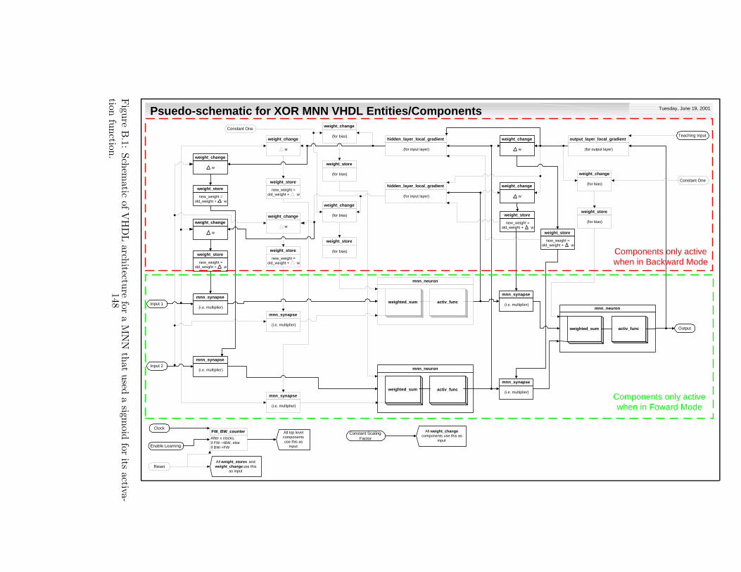
All weight_stores and weight_change use this
as input
Clock
Enable Learning
All top level components use this as
input
Teaching Input
Constant Scaling Factor
weight_change
w
weight_change
w
weight_change
w
mnn_synapse
(i.e. multiplier)
mnn_synapse
(i.e. multiplier)
weight_store
new_weight = old_weight + w
weight_store
new_weight = old_weight + w
Input 1
mnn_synapse
(i.e. multiplier)
mnn_synapse
(i.e. multiplier)
weight_store
new_weight = old_weight + w
weight_store
new_weight = old_weight + w
Input 2 mnn_neuron
weighted_sum activ_func
mnn_neuron
weighted_sum activ_func Output
All weight_change components use this as
input
weight_change
w
Tuesday, June 19, 2001 Psuedo-schematic for XOR MNN VHDL Entities/Components
Components only active when in Foward Mode
Components only active when in Backward Mode
Reset
FW_BW_counter
After x clocks, if FW ->BW, else if BW->FW
hidden_layer_local_gradient
(for input layer)
hidden_layer_local_gradient
(for input layer)
output_layer_local_gradient
(for output layer)
mnn_neuron
weighted_sum activ_func
weight_change
w
weight_store
new_weight = old_weight + w
weight_change
w
weight_store
new_weight = old_weight + w
mnn_synapse
(i.e. multiplier)
mnn_synapse
(i.e. multiplier)
weight_store
(for bias)
Constant One weight_change
(for bias)
weight_store
(for bias)
weight_change
(for bias)
weight_change
(for bias)
weight_store
(for bias)
Constant One
Figu
reB
.1:Sch
ematic
ofV
HD
Larch
itecture
fora
MN
Nth
atused
asigm
oidfor
itsactiva-
tionfu
nction
.148
Entity Name: FW BW counter
Input Signals: std logic clock
std logic learn enable
std logic reset
Output Signals: std logic FW BW
Internal Signals: std logic vector cycle counter
Dependencies: This component depends on the system clock of the FPGA device
used for this implementation.
Functional Purpose: This component is a small Finite State Machine, which emulates
the two states of a neural network - Forward Pass and Backward Pass of the Backpropagation
algorithm. The states FW and BW corresponds to the circuit reacting in accordance
with the Forward Pass and Backward Pass functionality respectively. Since the FW state
duration lasts until all Forward Pass related calculations are complete, and is based on the
propagation delay of the components involved with the Forward Pass, let nT represent the
time it takes for the FW state to compete, where T is the period of the clock cycle used,
and n is some constant which is determined from timing analysis performed on Forward
Pass implementation. Similarly, let mT represent the time it takes for the BW state to
complete, where m is some constant, which is determined from timing analysis of Backward
Pass implementation. Hence, using max (dme , dne), (where dxe represents the ceiling on
real number x) the FW BW counter can be represented by the following finite state
machines:
The FW BW counter can be implemented as a counter that counts clock cycles, and
reacts based on the state table:
,where
• X = don’t care conditions
precision floating-point standard, whereas std logic vector(15 downto 0) is a 16-bit construct used tosupport 16-bit fixed point
149
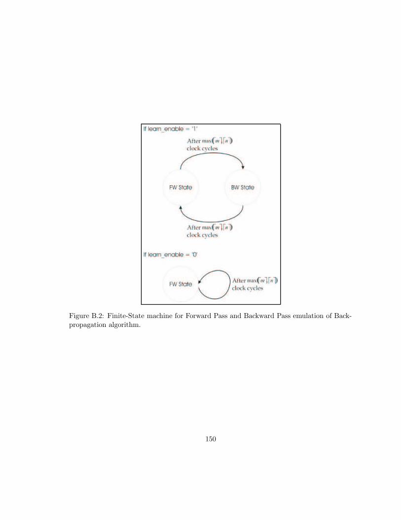
Figure B.2: Finite-State machine for Forward Pass and Backward Pass emulation of Back-propagation algorithm.
150

Inputs Current State Next Statereset clock learn enable FW BW cycle counter FW BW* cycle counter*
1 X X X X 1 Zero0 0 X X X FW BW cycle counter0 1 0 X < max (dme , dne) 1 cycle counter + 10 1 0 X = max (dme , dne) 1 Zero0 1 1 X < max (dme , dne) FW BW cycle counter + 10 1 1 X = max (dme , dne) FW BW Zero
• Zero = 00000000 if, for example, cycle counter was std logic vector(7 downto
0)
• FW BW = the state of the finite state machine, where ’0’ represents the BW state and
’1’ represents the FW state.
• cycle counter = an unsigned binary number, whose size is dependent on representing
the value max (dme , dne)
• reset = will ’RESET’ the circuit to FW state and cycle counter back to zero when
it has a value of logical ’1’.
• FW BW = the complement of FW BW.
• Note that the network can only learn (i.e. Backward Pass is enabled) when learn enable
= logical ’1’, otherwise the neural network is continually in Forward Pass mode (i.e.
FW BW always equals ’1’)
• **Note that all logic of the FW BW entity is synchronous with the rising edge of the
system clock, except for the reset signal, which is asynchronous (i.e. so reset can
occur at any time.)
Entity Name: weight store
Input Signals: std logic vector weight change
std logic BW enable
std logic reset
151
Output Signals: std logic vector synapse weight
Internal Signals: std logic vector weight value
std logic vector default weight
Dependencies: This component depends on FW BW counter and weight change
components.
Functional Purpose: This component will store a synapse weight, whose initializa-
tion value is implementation specific. All signals that are of type std logic vector, are
signed binary representations, whose sizes are implementation dependent. When reset is
a logical ’1’, the weight value is defaulted to the value stored in default weight. Only
when the circuit is in Backward Pass (i.e BW enable is a logical ’0’), will the weight be
updated according to the following equation:
w(s)kj (n) = w
(s)kj (n − 1) + ∆w
(s)kj (n)
, where
• wskj (n) = weight value = synapse weight that corresponds to the connection from
neuron unit j to k, in the sth layer of the neural net. This weight was calculated
during the nth Backward Pass of the backpropagation algorithm.
• wskj (n − 1) = (weight value*) = synapse weight that corresponds to the connection
from neuron unit j to k, in the sth layer of the neural net. This weight was calculated
during the (n − 1)th Backward Pass of the backpropagation algorithm.
• ∆w(s)kj (n) = weight change = change in weights corresponding the gradient of error
for connection from neuron unit j to k, in the sth layer of the neural net. This
weight change was calculated during the nth Backward Pass of the backpropagation
algorithm.
The weight store VHDL entity should adhere to the following state table:
152

Inputs Current State Next StateBW enable weight change reset synapse weight synapse weight*
X X 1 X default weight1 X 0 X synapse weight0 X 0 X synapse weight + weight change
, where
• X = don’t care conditions
• BW enable = a ’chip select’ which enables the weight store VHDL entity whenever
this signal is equal to logical ’0’ (i.e. in Backward Pass)
Entity Name: output layer local gradient
Input Signals: std logic vector teaching input
std logic vector neuron output
std logic BW enable
Output Signals: std logic vector local gradient
Internal Signals: std logic vector new gradient
Dependencies: This component depends on mnn neuron and FW BW counter com-
ponents.
Functional Purpose: This component is essentially the implementation of the local gradi-
ent function [20] for output layers, and implements for following function when in Backward
Pass (i.e. when BW enable is a logical ’0’):
δ(s)k = o
(s)k
(
1 − o(s)k
)(
tk − o(s)k
)
, where
• δ(s)k = local gradient = local gradient associated with the kth neuron, in the sth
layer in the neural net.
153

• o(s)k = neuron output = output of the kth neuron in the sth layer of the neural net,
when s = output layer.
• tk = teaching input = teaching input associated with kth neuron of output layer in
the neural network.
The output layer local gradient VHDL entity should adhere to the following state
table:
Inputs Current State Next StateBW enable teaching input neuron output new gradient new gradient*
1 X X X new gradient0 X X X Gradient Calculation
, where
• X = don’t care conditions
• BW enable = a ’chip select’ which enables the output layer local gradient VHDL
entity whenever this signal is equal to logical ’0’ (i.e. in Backward Pass)
• Gradient Calculation = (neuron output) × (1 − neuron output) ...
... × (teaching input− neuron output)
Entity Name: hidden layer local gradient
Input Signals: std logic vector gradient in3
std logic vector synaptic weight
std logic vector neuron output
std logic BW enable
3Note that there may be multiple versions of gradient in and synaptic weight (e.g. gradient in1,synaptic weight1, gradient in2, synaptic weight2, etc.) depending on how many connections the neuronoutput goes to.
154

Output Signals: std logic vector local gradient
Internal Signals: std logic vector new gradient
Dependencies: This component depends on mnn neuron component, FW BW counter
and could possibly encapsulate weighted sum.
Functional Purpose: This component is essentially the implementation of the local gra-
dient function for hidden layers, and implements for following function when in Backward
Pass (i.e. when BW enable is a logical ’0’):
δ(s)k = o
(s)k
(
1 − o(s)k
)
Ns−1∑
k
(
δ(s+1)k w
(s+1)kj
)
, where
• δ(s)k = local gradient = local gradient associated with the kth neuron, in the sth
layer in the neural net.
• δ(s+1)k = gradient in = local gradient associated with the kth neuron, in the (s + 1)th
layer in the neural net.
• o(s)k = neuron output = output of the kth neuron in the sth layer of the neural net,
when s = hidden layer.
• w(s+1)kj = synaptic weight = synapse weight that corresponds to the connection from
neuron unit j to k, in the (s + 1)th layer of the neural net.
Entity Name: weight change
Input Signals: std logic vector learning rate
std logic vector local gradient
std logic vector neuron output
155

std logic BW enable
Output Signals: std logic vector weight change
Internal Signals: std logic vector change value
Dependencies: This is dependent on mnn neuron, FW BW counter and out-
put layer local gradient or hidden layer local gradient components.
Functional Purpose: This is the implementation of the weight update function (i.e.
or cost function when used in the context of optimization) and implements the following
function when in Backward Pass (i.e. when BW enable is a logical ’0’):
∆w(s)kj = ηδ
(s)k o
(s−1)j
, where
• ∆w(s)kj = weight change = change in synapse weight that corresponds to the connec-
tion from neuron unit j to k, in the sth layer of the neural net.
• η = learning rate = a constant scaling factor for defining step size for gradient
descent.
• δ(s)k = local gradient = local gradient associated with the kth neuron, in the sth
layer in the neural net.
• o(s−1)j = neuron output = output of the kth neuron in the sth layer of the neural net,
when s = hidden layer.
The weight change VHDL entity should adhere to the following state table:
Inputs Current State Next StateBW enable other inputs weight change weight change*
1 X X weight change0 X X Change Calculation
, where
156

• X = don’t care conditions
• other inputs = all other inputs in the weight change VHDL entity, including
learning rate, local gradient, and neuron output.
• BW enable = a ’chip select’ which enables the weight change VHDL entity whenever
this signal is equal to logical ’0’ (i.e. in Backward Pass)
• Change Calculation = (learning rate) × (local gradient) × (neuron output)
Entity Name: weighted sum
Input Signals: std logic FW enable
std logic vector input a
std logic vector input b
Output Signals: std logic vector output
Internal Signals: std logic vector bias
Dependencies: This VHDL entity isn’t dependent on any other MNN entities.
Functional Purpose: This entity is used by mnn neuron to sum together input a,
input b and a constant bias. This VHDL entity only functions when in Forward Pass (i.e.
when FW enable is a logical ’1’), and adheres to the following state table:
Inputs Current State Next StateFW enable input a input b output output*
0 X X X output1 X X X Output Calculation
, where
• X = don’t care conditions
• FW enable = a ’chip select’ which enables the weighted sum VHDL entity whenever
this signal is equal to logical ’1’ (i.e. in Forward Pass)
157

• Output Calculation = (input a) + (input b) + (bias)
Entity Name: activ func
Input Signals: std logic FW enable
std logic vector input
Output Signals: std logic vector output
Internal Signals: std logic vector threshold
Dependencies: This VHDL entity isn’t dependent on any other MNN entities.
Functional Purpose: This is the implementation of the activation function [20]. This
VHDL entity implements the following step function when in Forward Pass (i.e. when
FW enable is a logical ’1’):
f(
H(s)k
)
=
{
1, if input > threshold
0, if input ≤ threshold
}
, where
• f(
H(s)k
)
= activation function
• threshold = a constant threshold that is application dependent.
Entity Name: mnn neuron
Input Signals: std logic enable
std vector logic incoming a
std vector logic incoming b
Output Signals: std vector logic outgoing
Internal Signals: std vector logic intermediate
158

Dependencies: This component depends on weighted sum and activ func VHDL
entities.
Functional Purpose: This is the implementation of a neuron, which performs the fol-
lowing functionality when in Forward Pass (i.e. when enable is a logical ’1’):
o(s)k = f
(
H(s)k
)
= f
Ns−1∑
j=1
w(s)kj o
(s−1)j + θ
(s)k
, where
• o(s)k = outgoing = output of the kth neuron in the sth layer of the neural net.
•∑Ns−1
j=1 w(s)kj o
(s−1)j = incoming a + incoming b = weighted sum of errors (from upper
layers only)
• θ(s)k = bias weight associated with the kth neuron in the sth layer of the neural net.
• H(s)k = intermediate = total weighted sum
Entity Name: mnn multiplier
Input Signals: std logic FW enable
std vector logic input a
std vector logic input b
Output Signals: std vector logic output
Internal Signals: None.
Dependencies: This component doesn’t depend on any other MNN components.
Functional Purpose: This is the implementation of a multiplier, which simply multiplies
input a and input b together when in Forward Pass (i.e. when enable is a logical ’1’).
159

Entity Name: mnn synapse
Input Signals: std logic FW enable
std vector logic incoming
std vector logic weight value
Output Signals: std vector logic outgoing
Internal Signals: None.
Dependencies: This component depends on mnn multiplier VHDL entity.
Functional Purpose: This is the implementation of a synapse, which simply multiplies
incoming and weight value together when in Forward Pass (i.e. when FW enable is a
logical ’1’).
160
Appendix C
Sample ANN Topology Def’n File
This appendix demonstrates the file format of two sample ANN Topology Definition Files
used by the RTR-MANN system. First, a user-defined ’input’ sample is given followed by
the associated ’output’ sample that was automatically generated by RTR-MANN thereafter.
The sample files shown in this appendix correspond to a 2-2-1 fully connected ANN topology
used to solve the ’XOR’ problem.
C.1 Sample ’Input’ File
ANN Topology Definition File is a text file with a pre-defined format, which contains decla-
rations of tunable parameters for the topology, training data, and other ANN-related data.
This type of file can be used as input into the RTR-MANN system, which is manually
defined by the user.
#RTR-MANN ANN DATA FILE USED TO SOLVE XOR PROBLEM
#IDENTICAL ANN TOPOLOGY AND TRAINING DATA USED
#IN NON-RTR PHASE OF MY THESIS
#KRIS NICHOLS - OCT. 5/2002
161
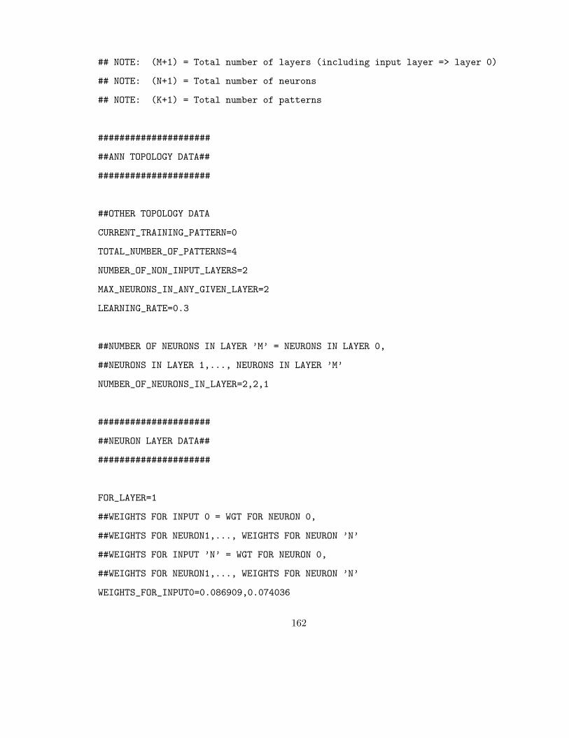
## NOTE: (M+1) = Total number of layers (including input layer => layer 0)
## NOTE: (N+1) = Total number of neurons
## NOTE: (K+1) = Total number of patterns
#####################
##ANN TOPOLOGY DATA##
#####################
##OTHER TOPOLOGY DATA
CURRENT_TRAINING_PATTERN=0
TOTAL_NUMBER_OF_PATTERNS=4
NUMBER_OF_NON_INPUT_LAYERS=2
MAX_NEURONS_IN_ANY_GIVEN_LAYER=2
LEARNING_RATE=0.3
##NUMBER OF NEURONS IN LAYER ’M’ = NEURONS IN LAYER 0,
##NEURONS IN LAYER 1,..., NEURONS IN LAYER ’M’
NUMBER_OF_NEURONS_IN_LAYER=2,2,1
#####################
##NEURON LAYER DATA##
#####################
FOR_LAYER=1
##WEIGHTS FOR INPUT 0 = WGT FOR NEURON 0,
##WEIGHTS FOR NEURON1,..., WEIGHTS FOR NEURON ’N’
##WEIGHTS FOR INPUT ’N’ = WGT FOR NEURON 0,
##WEIGHTS FOR NEURON1,..., WEIGHTS FOR NEURON ’N’
WEIGHTS_FOR_INPUT0=0.086909,0.074036
162

WEIGHTS_FOR_INPUT1=-0.126841,-0.130732
##BIAS = BIAS FOR NEURON 0,..., BIAS FOR NEURON ’N’
BIAS=-0.077525,0.093786
##NEURAL OUTPUT=OUTPUT FOR NEURON 0,
##OUTPUT FOR NEURON 1,..., OUTPUT FOR NEURON ’N’
NEURAL_OUTPUT=
##NEURAL ERROR FOR LAYER = ERR FOR NEURON 0,
##ERR FOR NEURON 1,...,ERROR FOR NEURON ’N’
NEURAL_ERROR=
FOR_LAYER=2
##WEIGHTS FOR INPUT 0 = WGT FOR NEURON 0,
##WEIGHTS FOR NEURON1,..., WEIGHTS FOR NEURON ’N’
##WEIGHTS FOR INPUT ’N’ = WGT FOR NEURON 0,
##WEIGHTS FOR NEURON1,..., WEIGHTS FOR NEURON ’N’
WEIGHTS_FOR_INPUT0=0.044572
WEIGHTS_FOR_INPUT1=-0.207922
##BIAS = BIAS FOR NEURON 0,..., BIAS FOR NEURON ’N’
BIAS=0.207083
##NEURAL OUTPUT=OUTPUT FOR NEURON 0,
##OUTPUT FOR NEURON 1,..., OUTPUT FOR NEURON ’N’
NEURAL_OUTPUT=
##NEURAL ERROR FOR LAYER = ERR FOR NEURON 0,
##ERR FOR NEURON 1,...,ERROR FOR NEURON ’N’
NEURAL_ERROR=
####################################
##INPUT & OUTPUT TRAINING PATTERNS##
####################################
163

##INPUT TRAINING PATTERN ’K’ = INPUT PATTERN FOR NEURON 0,
##INPUT PATTERN FOR NEURON 1,..., INPUT PATTERN FOR NEURON ’N’
INPUT_TRAINING_PATTERN0=0.0,0.0
INPUT_TRAINING_PATTERN1=0.0,1.0
INPUT_TRAINING_PATTERN2=1.0,0.0
INPUT_TRAINING_PATTERN3=1.0,1.0
##OUTPUT TRAINING PATTERN ’K’ = OUTPUT PATTERN FOR NEURON 0,
##OUTPUT PATTERN FOR NEURON 1,..., OUTPUT PATTERN FOR NEURON ’N’
OUTPUT_TRAINING_PATTERN0=0.0
OUTPUT_TRAINING_PATTERN1=1.0
OUTPUT_TRAINING_PATTERN2=1.0
OUTPUT_TRAINING_PATTERN3=0.0
################
##OUTPUT ERROR##
################
##OUTPUT NEURAL ERROR =ERROR FOR OUTPUT NEURON 0,
##ERROR FOR OUTPUT NEURON 1,..., ERROR FOR OUTPUT NEURON’N’
OUTPUT_NEURAL_ERROR=
C.2 Sample ’Output’ File
RTR-MANN automatically outputs a ANN Topology Definition File with updated values
after training / execution is complete. It’s essentially a log of the final results for the ANN
application under test, which the user can later analyze.
164

#ANN DATA FILE GENERATED BY RTR-MANN
## NOTE: (M+1) = Total number of layers (including input layer => layer 0)
## NOTE: (N+1) = Total number of neurons
## NOTE: (K+1) = Total number of patterns
#####################
##ANN TOPOLOGY DATA##
#####################
##OTHER TOPOLOGY DATA
CURRENT_TRAINING_PATTERN=2
TOTAL_NUMBER_OF_PATTERNS=4
NUMBER_OF_NON_INPUT_LAYERS=2
MAX_NEURONS_IN_ANY_GIVEN_LAYER=2
LEARNING_RATE=0.299804687500
##NUMBER OF NEURONS IN LAYER ’M’ = NEURONS IN LAYER 0,
##NEURONS IN LAYER 1,..., NEURONS IN LAYER ’M’
NUMBER_OF_NEURONS_IN_LAYER=2,2,1
#####################
##NEURON LAYER DATA##
#####################
FOR_LAYER=1
##WEIGHTS FOR INPUT 0 = wGT FOR NEURON 0,
##WEIGHTS FOR NEURON1,..., WEIGHTS FOR NEURON ’N’
##WEIGHTS FOR INPUT ’N’ = wGT FOR NEURON 0,
165

##WEIGHTS FOR NEURON1,..., WEIGHTS FOR NEURON ’N’
WEIGHTS_FOR_INPUT0=-2.601318359375,-5.162841796875
WEIGHTS_FOR_INPUT1=-2.647216796875,-5.166992187500
##BIAS = BIAS FOR NEURON 0,..., BIAS FOR NEURON ’N’
BIAS=-2.567626953125,1.435302734375
##NEURAL OUTPUT=OUTPUT FOR NEURON 0,
##OUTPUT FOR NEURON 1,..., OUTPUT FOR NEURON ’N’
NEURAL_OUTPUT=0.005615234375,0.023437500000
##NEURAL ERROR FOR LAYER = ERR FOR NEURON 0,
##ERR FOR NEURON 1,...,ERROR FOR NEURON ’N’
NEURAL_ERROR=0.000000000000,0.000000000000
FOR_LAYER=2
##WEIGHTS FOR INPUT 0 = wGT FOR NEURON 0,
##WEIGHTS FOR NEURON1,..., WEIGHTS FOR NEURON ’N’
##WEIGHTS FOR INPUT ’N’ = wGT FOR NEURON 0,
##WEIGHTS FOR NEURON1,..., WEIGHTS FOR NEURON ’N’
WEIGHTS_FOR_INPUT0=-2.646728515625
WEIGHTS_FOR_INPUT1=-7.846191406250
##BIAS = BIAS FOR NEURON 0,..., BIAS FOR NEURON ’N’
BIAS=3.246337890625
##NEURAL OUTPUT=OUTPUT FOR NEURON 0,
##OUTPUT FOR NEURON 1,..., OUTPUT FOR NEURON ’N’
NEURAL_OUTPUT=0.954589843750
##NEURAL ERROR FOR LAYER = ERR FOR NEURON 0,
##ERR FOR NEURON 1,...,ERROR FOR NEURON ’N’
NEURAL_ERROR=-0.000244140625
####################################
166
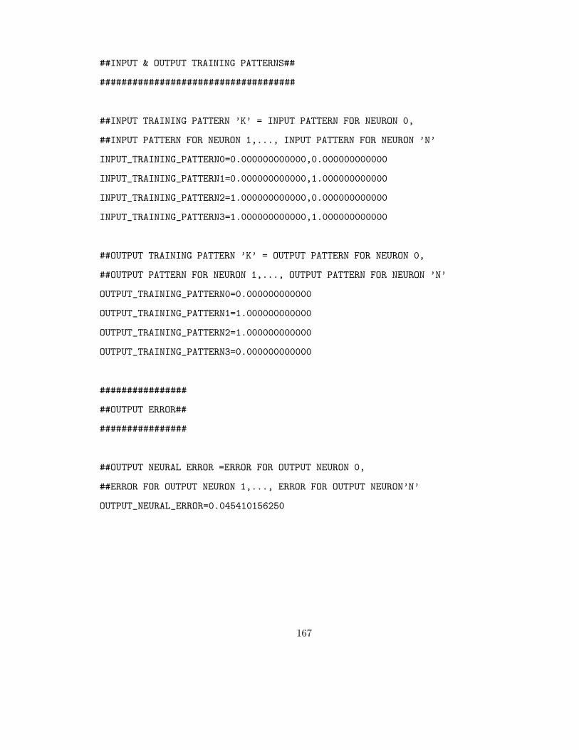
##INPUT & OUTPUT TRAINING PATTERNS##
####################################
##INPUT TRAINING PATTERN ’K’ = INPUT PATTERN FOR NEURON 0,
##INPUT PATTERN FOR NEURON 1,..., INPUT PATTERN FOR NEURON ’N’
INPUT_TRAINING_PATTERN0=0.000000000000,0.000000000000
INPUT_TRAINING_PATTERN1=0.000000000000,1.000000000000
INPUT_TRAINING_PATTERN2=1.000000000000,0.000000000000
INPUT_TRAINING_PATTERN3=1.000000000000,1.000000000000
##OUTPUT TRAINING PATTERN ’K’ = OUTPUT PATTERN FOR NEURON 0,
##OUTPUT PATTERN FOR NEURON 1,..., OUTPUT PATTERN FOR NEURON ’N’
OUTPUT_TRAINING_PATTERN0=0.000000000000
OUTPUT_TRAINING_PATTERN1=1.000000000000
OUTPUT_TRAINING_PATTERN2=1.000000000000
OUTPUT_TRAINING_PATTERN3=0.000000000000
################
##OUTPUT ERROR##
################
##OUTPUT NEURAL ERROR =ERROR FOR OUTPUT NEURON 0,
##ERROR FOR OUTPUT NEURON 1,..., ERROR FOR OUTPUT NEURON’N’
OUTPUT_NEURAL_ERROR=0.045410156250
167

Appendix D
Design Specifications for
RTR-MANN’s Feed-Forward Stage
D.1 Feed-forward Algorithm for Celoxica RC1000-PP
The control unit and datapath of RTR-MANN’s feed-forward stage was designed based on
the algorithm specified in this section. The following assumptions are made in order for the
Feed-forward algorithm to properly execute on the FPGA platform:
1. SoftCU has already Reconfigured the Celoxica RC1000-PP.
2. SoftCU has already pre-loaded Celoxica’s SRAM banks with correct data.
3. SoftCU has already reset circuit.
The following is a high-level description of the feed-forward algorithm, which was targeted
for execution on the Celoxica RC1000-PP:
1. For Each Non-Input Layer:
• Calculate activation function(
f(H(s)k )
)
, according to Equations 2.6 and 2.7 in
Section 2.4.2, using Eldredge’s Time-Multiplexed Interconnection Scheme [15].
168

(a) First, in order to feed activation values forward, one of the neurons on layer
m places its activation value on the [interconnection] bus.
(b) All neurons on layer m + 1 read this value from the bus and multiply it by
the appropriate weight storing the result.
(c) Then, the next neuron in layer m places its activation value in the bus.
(d) All of the neurons in layer m + 1 read this value and again multiply it by
the appropriate weight value.
(e) The neurons in layer m + 1 then accumulate this product with the product
of the previous multiply.
(f) This process is repeated until all of the neurons in layer m have had a chance
to transfer their activation values to the neurons in layer m + 1.
2. Calculate error term(
ε(M)k
)
for output layer only, according to Equation 2.9 in Sec-
tion 2.4.2.
The following is a more detailed pseudo-algorithm of how this feed-forward algorithm would
execute on the Celoxica platform:
1. Assumptions
Resetting the circuit results in the following:
• Sets all counters (e.g. layer counter, neuron counter, etc.) to zero
• Asserts reset signal of all neurons to logical ’1’
• Asserts reset signal of Memory Controller (MemCont) to ’1’
• Asserts reset signal of Address Generator (AddrGen) to ’1’
• Sets DONE flag to logical ’0’
2. Execution
Retrieve the following from memory: Number of Non-Input Layers,
169

Current Training Pattern, Total Number Of Patterns, and transfer this
data to TOTAL_LAYERS, pattern_counter, and TOTAL_PATTERNS registers
respectively.
Retrieve Number of Neurons for each layer, and transfer to
corresponding NUMNEURONSM register.
For layer_counter = n, where n = 0 to (TOTAL_LAYERS)
Determine Neurons in Layer (i.e. appropriate NUMNERONSM register
based on layer_counter)
Retrieve the following from memory: Biases for current layer
(based on neuron_counter)
Transfer biases to respective BIAS registers
if(layer_counter == 0) then
Retrieve the following from memory: Input Training Patterns
(based on Current Training Pattern)
Transfer Input Patterns to respective NEURON_OUTPUTM registers
End if;
De-assert resets signal for each neuron entity, sets output of
entity equal to bias
For neuron_counter = i, where i = 0 to (Neurons in Layer+1)
Retrieve the following from memory: Neuron Weights for Input
i (based on layer_counter and neuron_counter)
Transfer weights to respective WGT registers
switch(layer_counter)
case 0:
170

Do each of the following statements in parallel(i.e.
like separate threads in software):
switch(neuron_counter)
case (Neurons in Layer+1):
break;
default:
Transfer NEURON_OUTPUTi to INPUT register
If(neuron_counter>0)
Assert chip_enable signal on neuron entity
to let it accumulate inputs, which signals
when done one accumulation calculation.
End if;
End parallel;
Break;
case TOTAL_LAYERS:
if(neuron_counter >= 2) &&
(neuron_counter <= Neurons in Layer + 1)
transfer Output Error Generator results to
OutputPattern(i-2);
which is the same as saying
OUTPUT_PATTERN(i-2) = OUTPUT_PATTERN(i-2) -
NeuronOutBus (via Output Err Generator);
End if;
If(neuron_counter >= 1) &&
(neuron_counter <= Neurons in Layer)
Transfer Activation Function output to NeuronOutBus
(i.e. input to Output Error Generator);
Transfer Activation Function output to
NEURON_OUTPUT(i-1)
171

End if;
if(neuron_counter >=0) &&
(neuron_counter <= Neurons in Layer-1)
transfer NEURON_OUTPUTi to WgtSumBus (i.e. input
for Activation Function);
end if;
break;
default:
if(neuron_counter >=2) &&
(neuron_counter <= Neurons in Layer+1)
transfer INPUT register contents to all NeuronN
accumulators;
transfer INPUT to NEURON_OUTPUT(i-2) register;
end if;
if(neuron_counter >=1) &&
(neuron_counter <= Neurons in Layer)
transfer Activation Function output to INPUT
register;
end if;
if(neuron_counter >=0) &&
(neuron_counter <= Neurons in Layer-1)
transfer NEURON_OUTPUTi to WgtSumBus (i.e. input
for Activation Function);
end if;
end switch;
Increment neuron_counter;
End for;
switch(layer_counter)
172

case 0: // move weight sums in layer_counter into
//appropriate NEURON_OUTPUT registers
NEURON_OUTPUTi = NEURONi;
Break;
case TOTAL_LAYERS:
//write activation output from (layer_counter-1)
//to memory
Write all NEURON_OUTPUTi registers to "Neural Output
in Layer (layer_counter-1)" memory;
Write all OUTPUT_PATTERNi registers to "Error for
Output Neuron i" memory;
Break;
Default:
//write activation output from (layer_counter-1)
//to memory
Write all NEURON_OUTPUTi registers to Neural Output
in Layer (layer_counter-1)memory;
//move weight sums in layer_counter into appropriate
//NEURON_OUTPUT registers
NEURON_OUTPUTi = NEURONi;
Break;
end switch;
//De-assert chip_enable signal on neuron entity to stop
//it from accumulating anymore inputs.
//Retrieve the following from memory: Output Training
//Patterns (based on Current Training Pattern)
//Transfer Output Training Patterns to OUTPUT_PATTERNi register
/*For neuron_counter = i, where i = 0 to Neurons in Layer
173

Transfer output of Neuron i to Netbus (i.e. Activation
Function), and wait 1 clk cycle
Transfer resulting output of Activation Function to
NEURON_OUTPUTi register
Start in parallel (i.e. like a thread in software):
if(layer_counter == number of Non-Input Neurons) then
OUTPUT_PATTERNi = OUTPUT_PATTERNi - NEURON_OUTPUTi
(via Output Err Generator)
End if;
End in parallel;
Increment neuron_counter;
End for;
/*
Increment layer_counter
Assert reset signal for each neuron
End for;
/*
Write all OUTPUT_PATTERNi registers (which contain neural
output error) to memory.
*/
Set DONE signal to logical 1, which notifies SoftCU that
processing is finished.
174
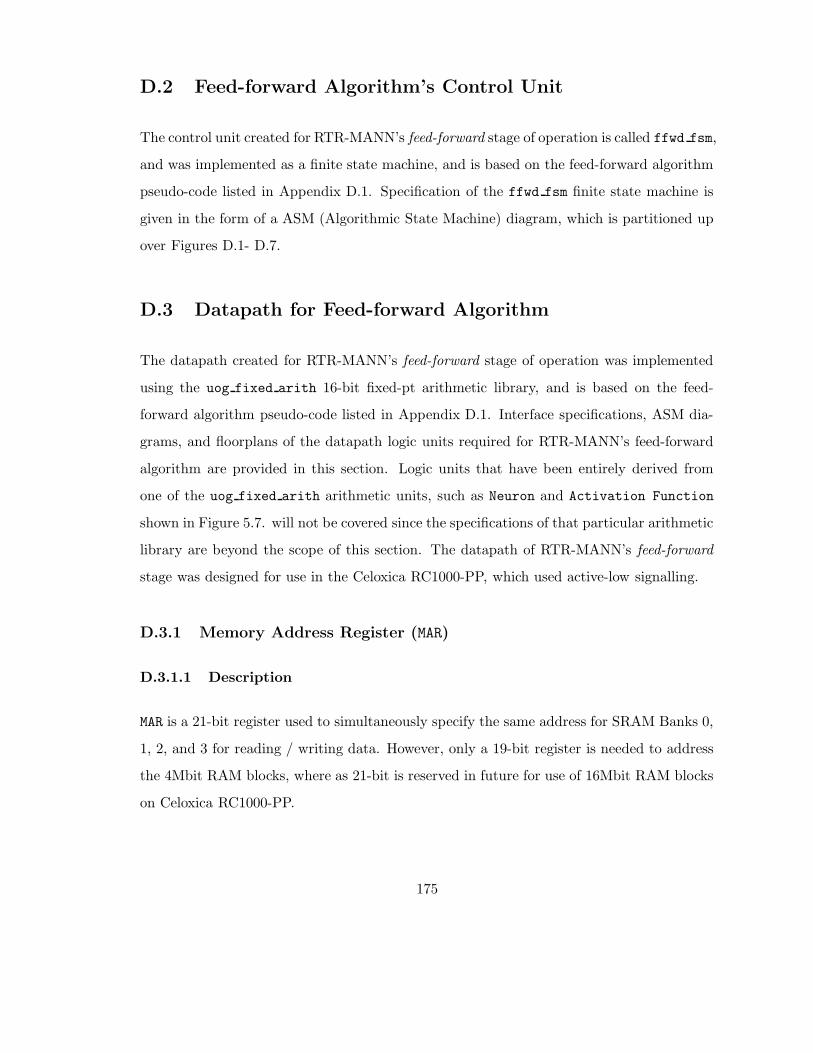
D.2 Feed-forward Algorithm’s Control Unit
The control unit created for RTR-MANN’s feed-forward stage of operation is called ffwd fsm,
and was implemented as a finite state machine, and is based on the feed-forward algorithm
pseudo-code listed in Appendix D.1. Specification of the ffwd fsm finite state machine is
given in the form of a ASM (Algorithmic State Machine) diagram, which is partitioned up
over Figures D.1- D.7.
D.3 Datapath for Feed-forward Algorithm
The datapath created for RTR-MANN’s feed-forward stage of operation was implemented
using the uog fixed arith 16-bit fixed-pt arithmetic library, and is based on the feed-
forward algorithm pseudo-code listed in Appendix D.1. Interface specifications, ASM dia-
grams, and floorplans of the datapath logic units required for RTR-MANN’s feed-forward
algorithm are provided in this section. Logic units that have been entirely derived from
one of the uog fixed arith arithmetic units, such as Neuron and Activation Function
shown in Figure 5.7. will not be covered since the specifications of that particular arithmetic
library are beyond the scope of this section. The datapath of RTR-MANN’s feed-forward
stage was designed for use in the Celoxica RC1000-PP, which used active-low signalling.
D.3.1 Memory Address Register (MAR)
D.3.1.1 Description
MAR is a 21-bit register used to simultaneously specify the same address for SRAM Banks 0,
1, 2, and 3 for reading / writing data. However, only a 19-bit register is needed to address
the 4Mbit RAM blocks, where as 21-bit is reserved in future for use of 16Mbit RAM blocks
on Celoxica RC1000-PP.
175

Table D.1: MAR FPGA floorplan for Celoxica RC1000-PPMAR Bits Celoxica RC1000-PP I/O PinMAR 0 FA0 2, FA1 2, FA2 2, and FA3 2MAR 1 FA0 3, FA1 3, FA2 3, and FA3 3MAR 2 FA0 4, FA1 4, FA2 4, and FA3 4MAR 3 FA0 5, FA1 5, FA2 5, and FA3 5MAR 4 FA0 6, FA1 6, FA2 6, and FA3 6MAR 5 FA0 7, FA1 7, FA2 7, and FA3 7MAR 6 FA0 8, FA1 8, FA2 8, and FA3 8MAR 7 FA0 9, FA1 9, FA2 9, and FA3 9MAR 8 FA0 10, FA1 10, FA2 10, and FA3 10MAR 9 FA0 11, FA1 11, FA2 11, and FA3 11MAR 10 FA0 12, FA1 12, FA2 12, and FA3 12MAR 11 FA0 13, FA1 13, FA2 13, and FA3 13MAR 12 FA0 14, FA1 14, FA2 15, and FA3 15MAR 13 FA0 15, FA1 15, FA2 15, and FA3 15MAR 14 FA0 16, FA1 16, FA2 16, and FA3 16MAR 15 FA0 17, FA1 17, FA2 17, and FA3 17MAR 16 FA0 18, FA1 18, FA2 18, and FA3 18MAR 17 FA0 19, FA1 19, FA2 19, and FA3 19MAR 18 FA0 20, FA1 20, FA2 20, and FA3 20MAR 19 FA0 21, FA1 21, FA2 21, and FA3 21MAR 20 FA0 22, FA1 22, FA2 22, and FA3 22
D.3.1.2 FPGA Floormapping of Register
This register is mapped to the SRAM address ports on the Celoxica RC1000-PP (refer to
RC1000-PP Hardware Reference Manual [28]), as shown in Table D.1.
D.3.2 Memory Buffer Register 0 – 7 (MB0 - MB7)
D.3.2.1 Description
Eight memory buffers, called MB0 - MB7, were each implemented as a 16-bit register, and
whose purpose was to temporarily store data read from, or to be written to the Celoxica
RC1000-PP SRAM banks.
D.3.2.2 FPGA Floormapping of Register
Each register is mapped from SRAM data port on the Celoxica RC1000-PP (refer to
RC1000-PP Hardware Reference Manual [28]), as shown in Tables D.2 and D.3.
176

Table D.2: MBn(where n = 0, 2, 4, 6) FPGA floorplan for Celoxica RC1000-PPMBn Bits (where n = 0, 2, 4, 6) Celoxica RC1000-PP I/O PinMBn 0 FDn 0MBn 1 FDn 1MBn 2 FDn 2MBn 3 FDn 3MBn 4 FDn 4MBn 5 FDn 5MBn 6 FDn 6MBn 7 FDn 7MBn 8 FDn 8MBn 9 FDn 9MBn 10 FDn 10MBn 11 FDn 11MBn 12 FDn 12MBn 13 FDn 13MBn 14 FDn 14MBn 15 FDn 15
Table D.3: MBn(where n = 1, 3, 5, 7) FPGA floorplan for Celoxica RC1000-PPMBn Bits (where n = 1, 3, 5, 7) Celoxica RC1000-PP I/O PinMBn 0 FDn 16MBn 1 FDn 17MBn 2 FDn 18MBn 3 FDn 19MBn 4 FDn 20MBn 5 FDn 21MBn 6 FDn 22MBn 7 FDn 23MBn 8 FDn 24MBn 9 FDn 25MBn 10 FDn 26MBn 11 FDn 27MBn 12 FDn 28MBn 13 FDn 29MBn 14 FDn 30MBn 15 FDn 31
177

Table D.4: MRW FPGA floorplan for Celoxica RC1000-PPMRW Bits Celoxica RC1000-PP I/O Pin Control Description
MRW 0 WE0 L, inverse(OE0 L) Read / Write control for SRAM Bank 0MRW 1 WE1 L, inverse(OE1 L) Read / Write control for SRAM Bank 1MRW 2 WE2 L, inverse(OE2 L) Read / Write control for SRAM Bank 2MRW 3 WE3 L, inverse(OE3 L) Read / Write control for SRAM Bank 3∗∗∗ NOTE: All WEn L and OEn L pins are active-low, which means they are active when
asserted low (i.e. asserted to logical ’0’).
D.3.3 Memory Read / Write Register (MRW)
D.3.3.1 Description
MRW is a 4-bit register used to choose ’read’ or ’write’ mode for each of the SRAM Banks
0-4.
D.3.3.2 FPGA Floormapping of Register
Each register is mapped to SRAM Control ports on the Celoxica RC1000-PP (refer to
RC1000-PP Hardware Reference Manual [28]), as shown in Tables D.4.
D.3.4 Memory Chip Enable Register (MCE)
D.3.4.1 Description
MCE is a 4-bit register used to ’enable’ each memory bank for reading / writing individually.
D.3.4.2 FPGA Floormapping of Register
Each register is mapped to SRAM Enable ports on the Celoxica RC1000-PP (refer to
RC1000-PP Hardware Reference Manual [28]), as shown in Tables D.5.
178

Table D.5: MCE FPGA floorplan for Celoxica RC1000-PPMCE Bits Celoxica RC1000-PP I/O Pin Enable DescriptionMCE 0 CE0 L0, CE0 L1, CE0 L2, CE0 L3 Enables SRAM Bank 0MCE 1 CE1 L0, CE1 L1, CE1 L2, CE1 L3 Enables SRAM Bank 1MCE 2 CE2 L0, CE2 L1, CE2 L2, CE2 L3 Enables SRAM Bank 2MCE 3 CE3 L0, CE3 L1, CE3 L2, CE3 L3 Enables SRAM Bank 3∗∗∗ NOTE: All CEn 0, CEn 1 CEn 2, and CEn 3 pins are active-low, which
means they are active when asserted low (i.e. asserted to logical ’0’).
Table D.6: MOWN FPGA floorplan for Celoxica RC1000-PPMOWN Bits Celoxica RC1000-PP I/O Pin Ownership DescriptionMOWN 0 REQn L, where n = 0, 1, 2, 3 Request for ownership
of all SRAM BanksMOWN 1 GNT0 L AND GNT1 L Flags when ownership
AND GNT2 L AND GNT3 L is granted∗∗∗ NOTE: All REQn L and GNTn L pins are active-low, which means they are
active when asserted low (i.e. asserted to logical ’0’).
D.3.5 Memory Ownership Register (MOWN)
D.3.5.1 Description
MOWN is a 2-bit register used by the FPGA to request ownership of memory, before it can
be either read or written. SRAM Banks on the Celoxica Platform can be owned by either
the host PC or FPGA, but not both.
D.3.5.2 FPGA Floormapping of Register
Each register is mapped to SRAM Arbitration ports on the Celoxica RC1000-PP (refer to
RC1000-PP Hardware Reference Manual [28]), as shown in Tables D.6.
D.3.6 Reset Signal (RESET)
D.3.6.1 Description
RESET is a 1-bit signal under control of SoftCU and is used to reset the circuit.
179

Table D.7: RESET FPGA floorplan for Celoxica RC1000-PPRESET Bits Celoxica RC1000-PP I/O PinRESET PLX USER1
Table D.8: DONE FPGA floorplan for Celoxica RC1000-PPDONE Bits Celoxica RC1000-PP I/O PinDONE PLX USER0
D.3.6.2 FPGA Floormapping of Register
Each register is mapped to PLX User I/O on the Celoxica RC1000-PP (refer to RC1000-PP
Hardware Reference Manual [28]), as shown in Tables D.7.
D.3.7 DONE Signal (DONE)
D.3.7.1 Description
DONE is a 1-bit signal that acts as a flag to SoftCU, which signals when feed-forward stage
processing has completed.
D.3.7.2 FPGA Floormapping of Register
Each register is mapped to PLX User I/O on the Celoxica RC1000-PP (refer to RC1000-PP
Hardware Reference Manual [28]), as shown in Tables D.8.
D.3.8 Celoxica RC1000-PP Case Study: Writing Data From FPGA To
SRAM Banks Simultaneously
FPGA can read / write all four 32-bit memory banks simultaneously. For RTR-MANN,
this means that eight 16-bit neuron weight values can be read from memory simultaneously.
Please refer to sections 6, 12.9, and 12.10 of Celoxica RC1000-PP Hardware Manual [28] for
more information regarding memory bank interfacing. This case study demonstrates how
the FPGA on the RC1000-PP platform can write data to memory. This can be used as a
180

sample to test the platform with, or can be used as a reference for more complex designs
on the RC1000-PP platform.
D.3.8.1 Initial Conditions
This case study assumes the following initial conditions:
1. RC1000-PP has been reset (i.e. host PC has ownership of memory banks on power-
up).
2. FPGA has already been reconfigured with circuit.
3. Host PC has signalled the release of ownership over the RC1000-PP’s memory.
D.3.8.2 Proposed Algorithm
The proposed algorithm for this case study is based on the available hardware I/O resources
described in Celoxica RC1000-PP Hardware Manual [28], which is carried out as follows:
STEP#1: Disable SRAM chip enable bits (i.e. set CE0 L0-CE0 3, CE1 L0-CE1 L3,
CE2 L0-CE2 L3, and CE3 L0-CE3 L3 to ’1’).
STEP#2: Disable WRITE ENABLE SRAM control bits (i.e. set WE0 L-WE3 L to ’1’) and
disable OUTPUT ENABLE SRAM control bits (i.e. set WE0 L-OE3 L to ’1’).
STEP#3: FPGA must assert all REQn signals (i.e. REQ0-REQ3 set to ’0’).
STEP#4: FPGA waits until all GNTn signals (i.e. wait until GNT0-GNT3 set to ’0’)
STEP#5: Place desired data on SRAM 0 DATA – SRAM 3 DATA memory ports.
STEP#6: Select desired address to write to on each memory bank; set SRAM 0 Address
– SRAM 3 Address memory ports.
181
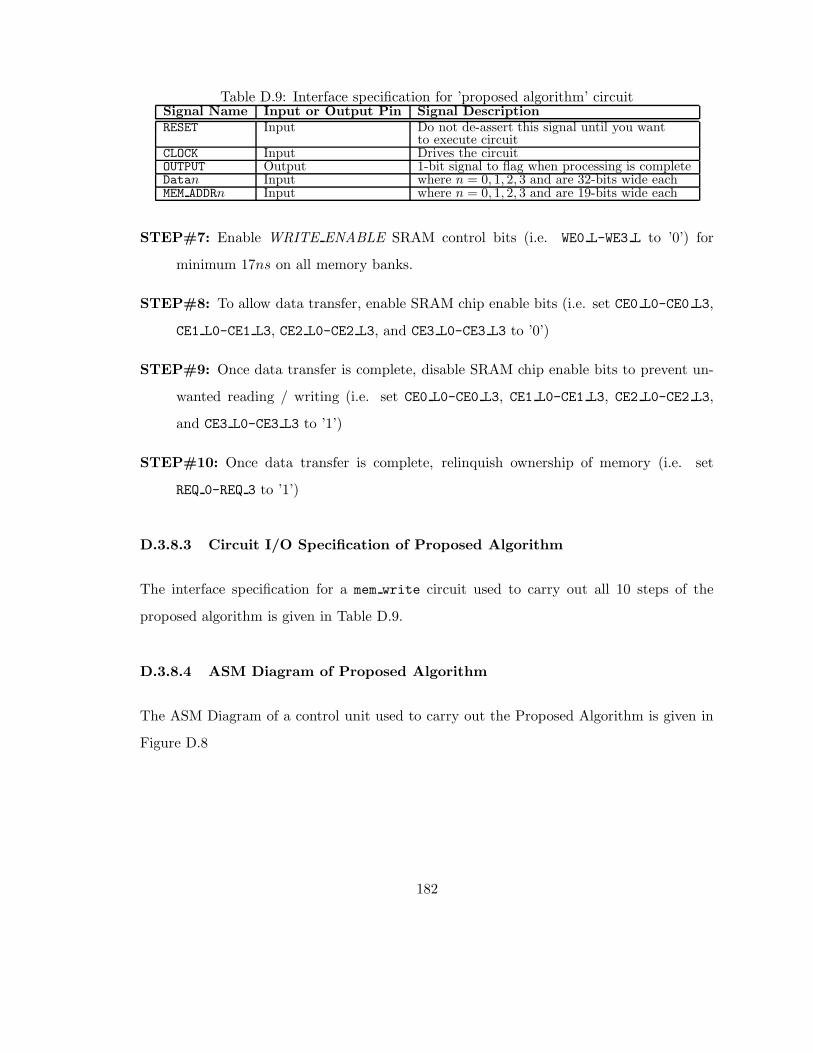
Table D.9: Interface specification for ’proposed algorithm’ circuitSignal Name Input or Output Pin Signal DescriptionRESET Input Do not de-assert this signal until you want
to execute circuitCLOCK Input Drives the circuitOUTPUT Output 1-bit signal to flag when processing is completeDatan Input where n = 0, 1, 2, 3 and are 32-bits wide eachMEM ADDRn Input where n = 0, 1, 2, 3 and are 19-bits wide each
STEP#7: Enable WRITE ENABLE SRAM control bits (i.e. WE0 L-WE3 L to ’0’) for
minimum 17ns on all memory banks.
STEP#8: To allow data transfer, enable SRAM chip enable bits (i.e. set CE0 L0-CE0 L3,
CE1 L0-CE1 L3, CE2 L0-CE2 L3, and CE3 L0-CE3 L3 to ’0’)
STEP#9: Once data transfer is complete, disable SRAM chip enable bits to prevent un-
wanted reading / writing (i.e. set CE0 L0-CE0 L3, CE1 L0-CE1 L3, CE2 L0-CE2 L3,
and CE3 L0-CE3 L3 to ’1’)
STEP#10: Once data transfer is complete, relinquish ownership of memory (i.e. set
REQ 0-REQ 3 to ’1’)
D.3.8.3 Circuit I/O Specification of Proposed Algorithm
The interface specification for a mem write circuit used to carry out all 10 steps of the
proposed algorithm is given in Table D.9.
D.3.8.4 ASM Diagram of Proposed Algorithm
The ASM Diagram of a control unit used to carry out the Proposed Algorithm is given in
Figure D.8
182
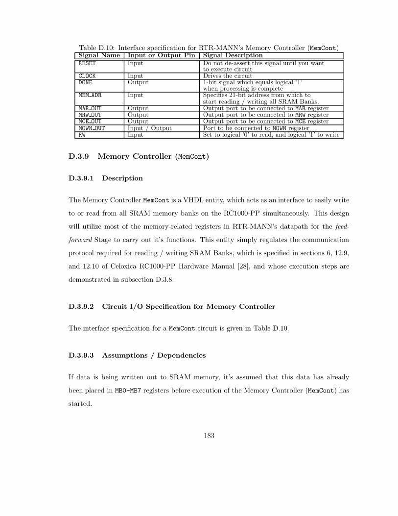
Table D.10: Interface specification for RTR-MANN’s Memory Controller (MemCont)Signal Name Input or Output Pin Signal DescriptionRESET Input Do not de-assert this signal until you want
to execute circuitCLOCK Input Drives the circuitDONE Output 1-bit signal which equals logical ’1’
when processing is completeMEM ADR Input Specifies 21-bit address from which to
start reading / writing all SRAM Banks.MAR OUT Output Output port to be connected to MAR registerMRW OUT Output Output port to be connected to MRW registerMCE OUT Output Output port to be connected to MCE registerMOWN OUT Input / Output Port to be connected to MOWN registerRW Input Set to logical ’0’ to read, and logical ’1’ to write
D.3.9 Memory Controller (MemCont)
D.3.9.1 Description
The Memory Controller MemCont is a VHDL entity, which acts as an interface to easily write
to or read from all SRAM memory banks on the RC1000-PP simultaneously. This design
will utilize most of the memory-related registers in RTR-MANN’s datapath for the feed-
forward Stage to carry out it’s functions. This entity simply regulates the communication
protocol required for reading / writing SRAM Banks, which is specified in sections 6, 12.9,
and 12.10 of Celoxica RC1000-PP Hardware Manual [28], and whose execution steps are
demonstrated in subsection D.3.8.
D.3.9.2 Circuit I/O Specification for Memory Controller
The interface specification for a MemCont circuit is given in Table D.10.
D.3.9.3 Assumptions / Dependencies
If data is being written out to SRAM memory, it’s assumed that this data has already
been placed in MB0-MB7 registers before execution of the Memory Controller (MemCont) has
started.
183
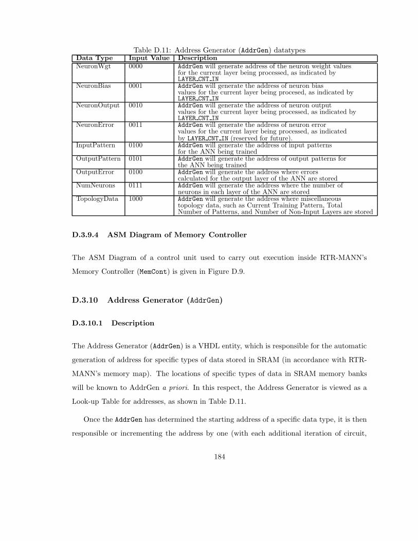
Table D.11: Address Generator (AddrGen) datatypesData Type Input Value DescriptionNeuronWgt 0000 AddrGen will generate address of the neuron weight values
for the current layer being processed, as indicated byLAYER CNT IN
NeuronBias 0001 AddrGen will generate the address of neuron biasvalues for the current layer being procesed, as indicated byLAYER CNT IN
NeuronOutput 0010 AddrGen will generate the address of neuron outputvalues for the current layer being processed, as indicated byLAYER CNT IN
NeuronError 0011 AddrGen will generate the address of neuron errorvalues for the current layer being processed, as indicatedby LAYER CNT IN (reserved for future).
InputPattern 0100 AddrGen will generate the address of input patternsfor the ANN being trained
OutputPattern 0101 AddrGen will generate the address of output patterns forthe ANN being trained
OutputError 0100 AddrGen will generate the address where errorscalculated for the output layer of the ANN are stored
NumNeurons 0111 AddrGen will generate the address where the number ofneurons in each layer of the ANN are stored
TopologyData 1000 AddrGen will generate the address where miscellaneoustopology data, such as Current Training Pattern, TotalNumber of Patterns, and Number of Non-Input Layers are stored
D.3.9.4 ASM Diagram of Memory Controller
The ASM Diagram of a control unit used to carry out execution inside RTR-MANN’s
Memory Controller (MemCont) is given in Figure D.9.
D.3.10 Address Generator (AddrGen)
D.3.10.1 Description
The Address Generator (AddrGen) is a VHDL entity, which is responsible for the automatic
generation of address for specific types of data stored in SRAM (in accordance with RTR-
MANN’s memory map). The locations of specific types of data in SRAM memory banks
will be known to AddrGen a priori. In this respect, the Address Generator is viewed as a
Look-up Table for addresses, as shown in Table D.11.
Once the AddrGen has determined the starting address of a specific data type, it is then
responsible or incrementing the address by one (with each additional iteration of circuit,
184

and if START is enabled). Each additional increment corresponds to the address of the next
six values, or row across all SRAM banks, of the same data type in sequential order. If no
more values of this same data type (i.e. no more additional addresses) exist, the AddrGen
will set it’s OUT OF RANGE signal to logical ’1’.
D.3.10.2 Assumptions / Dependencies
The Address Generator (AddrGen) is highly dependent on the static memory architecture
used for RTR-MANN’s feed-forward stage. If the design of this static memory architecture
changes in the future, so too will the design of AddrGen change.
D.3.10.3 ASM Diagram for Address Generator (AddrGen)
The ASM Diagram of a control unit used to carry out execution inside RTR-MANN’s
Address Generator (AddrGen) is given in Figure D.10.
185

AddrGen:START<-0 AddrGen:RESET<-1
AddrGen:DATA_TYPE<-NumNeurons i:=0
FFWD_NN1
AddrGen:Reset <- 0
FFWD_NN2
AddrGen:DONE
RESET
DONE<- 0 layer_counter <-1 neuron_counter<-0 pattern_counter <-0 NeuralReset<-1 Neuron[0,..., N ]:Start<-0 //Ensures no continuous iteration of MAC calcs,
//where N=max Neuron registers instantiated AddrGen:START <- 0 //Ensures no false address offset is generated AddrGen:RESET <- 1 MemCont:RESET <- 1
FFWD_INIT 1
MBn:din <- "ZZZZZZZZZZZZZZZZ" ; n=0,...,7 //high impedance or floatingallows Celoxica RC1000
memory //to write to memory buffer registers (i.e. MBn)
AddrGen:DATA_TYPE <- TopologyData
FFWD_OTD1
FFWD_OTD2
AddrGen:RESET <- 0
AddrGen:DONE
FFWD_OTD3
MemCont:RW<-0 //read from memory
FFWD_OTD4
MemCont:RESET<-0
MemCont:DONE
FFWD_OTD5
MemCont:RESET<-1
FFWD_OTD6
pattern_counter := MB0:dout TOTAL_PATTERNS := MB1:dout TOTAL_LAYERS := (MB2:dout+1)//NON-INPUT LAYERS+1 MAX_NEURONS := MB3:dout AddrGen:MAX_LAYERS<-TOTAL_LAYERS AddrGen:MAX_PATTERNS<-TOTAL_PATTERNS AddrGen:MAX_NEURONS<-MAX_NEURONS AddrGen:PATT_CNT_IN<- pattern_counter AddrGen:LAYER_CNT_IN<-layer_counter AddrGen:NEURON_CNT_IN<-neuron_counter
0
AddrGen:OUT_OF_ RANGE
1
1 Go To FFWD_GETBIAS1
MemCont:RW<-0 //read from memory
FFWD_NN3 0
FFWD_NN4
MemCont:RESET<-0
MemCont:DONE
If((n +8*i)<TOTAL_LAYERS) NUMNEURONS[n+8*i]<-MBn:dout // where n=0,...,7
FFWD_NN5
i:=i+1 AddrGen:START <- 1 MemCont:RESET <- 1
FFWD_NN6
AddrGen:START <- 0
FFWD_NN7
**NOTE: FFWD_OTD = Other Traning Data FFWD_NN = Number of Neurons (for each layer)
ASM diagrams with VHDL pseudo-code for FFWD_FSM module
Figure D.1: ASM diagram for ffwd fsm control unit (Part 1 of 7)
186
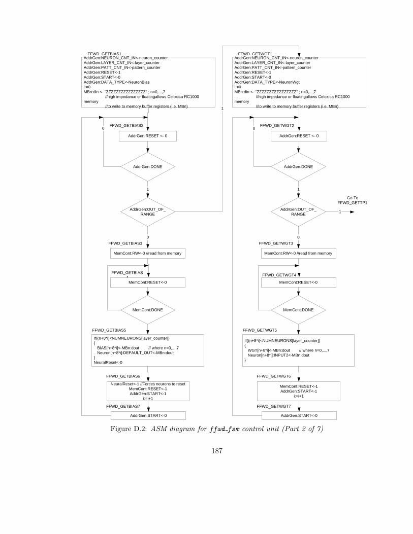
AddrGen:NEURON_CNT_IN<-neuron_counter AddrGen:LAYER_CNT_IN<-layer_counter AddrGen:PATT_CNT_IN<-pattern_counter AddrGen:RESET<-1 AddrGen:START<-0 AddrGen:DATA_TYPE<-NeuronBias i:=0 MBn:din <- "ZZZZZZZZZZZZZZZZ" ; n=0,...,7
//high impedance or floatingallows Celoxica RC1000 memory
//to write to memory buffer registers (i.e. MBn)
FFWD_GETBIAS1
FFWD_GETBIAS2
AddrGen:RESET <- 0
AddrGen:DONE
FFWD_GETBIAS3
MemCont:RW<-0 //read from memory
FFWD_GETBIAS 4
MemCont:RESET<-0
MemCont:DONE
FFWD_GETBIAS5
NeuralReset<-1 //Forces neurons to reset MemCont:RESET<-1 AddrGen:START<-1
i:=i+1
FFWD_GETBIAS6
If((n+8*i)<NUMNEURONS[layer_counter]) { BIAS[n+8*i]<-MBn:dout // where n=0,...,7 Neuron[n+8*i]:DEFAULT_OUT<-MBn:dout } NeuralReset<-0
AddrGen:OUT_OF_ RANGE
1
0
1
0
AddrGen:START<-0
FFWD_GETBIAS7
AddrGen:NEURON_CNT_IN<-neuron_counter AddrGen:LAYER_CNT_IN<-layer_counter AddrGen:PATT_CNT_IN<-pattern_counter AddrGen:RESET<-1 AddrGen:START<-0 AddrGen:DATA_TYPE<-NeuronWgt i:=0 MBn:din <- "ZZZZZZZZZZZZZZZZ" ; n=0,...,7
//high impedance or floatingallows Celoxica RC1000 memory
//to write to memory buffer registers (i.e. MBn)
FFWD_GETWGT1
FFWD_GETWGT2
AddrGen:RESET <- 0
AddrGen:DONE
FFWD_GETWGT3
MemCont:RW<-0 //read from memory
FFWD_GETWGT4
MemCont:RESET<-0
MemCont:DONE
FFWD_GETWGT5
MemCont:RESET<-1 AddrGen:START<-1
i:=i+1
FFWD_GETWGT6
If((n+8*i)<NUMNEURONS[layer_counter]) { WGT[n+8*i]<-MBn:dout // where n=0,...,7 Neuron[n+8*i]:INPUT2<-MBn:dout }
AddrGen:OUT_OF_ RANGE
1
0
1
0
AddrGen:START<-0
FFWD_GETWGT7
Go To FFWD_GETTP1
Figure D.2: ASM diagram for ffwd fsm control unit (Part 2 of 7)
187

layer_counter
FFWD_N_SUM1
INPUT<-NEURONOUTPUT[neuron_counter] when (neuron_counter<NUMNEURONS[layer_counter -1]) AND (neuron_counter>=0) (Neuron[0,...,N]:Start <- 1) AND (NeuralReset <- 0) AND (Neuron[0,...,N]:INPUT1 <- NEURONOUTPUT[neuron_counter]) when (neuron_counter > 0) AND (neuron_counter < NUMNEURONS[layer_counter-1])
FFWD_INIT_PIPE1 1
Neuron[0,...,N]:Start<-0 //Ensures no continuous iteration of MAC calcs, //where N=max Neuron registers instantiated
FFWD_INIT_PIPE2
Neuron[0,...,N]:DONE when (neuron_counter <= 0) AND (neuron_counter
< NUMNEURONS[layer_counter-1]) else 1
0
neuron_counter <- neuron_counter + 1
FFWD_INIT_PIPE3 1
neuron_counter <- neuron_counter + 1
FFWD_INIT_PIPE4
neuron_counter
(NUMNEURONS[layer_counter-1]) OR
(NUMNEURONS[layer_counter- 1]+1)
(< NUMNEURONS[layer_counter - 1])
(>NUMNEURONS[layer_counter- 1]+1)
GO TO FFWD_GETWGT1
neuron_counter 1
NOT(1)
GO TO FFWD_WR_NO1
GO TO FFWD_END_PIPE1
(1 < layer_counter < TOTAL_LAYERS)
TOTAL_LAYER S
Go To FFWD_HID_PIPE1
Go To FFWD_OUT_PIPE1
**NOTE: FFWD_INIT_PIPE = PIPELINE for INPUT LAYER FFWD_HID_PIPE = PIPELINE for HIDDEN LAYER FFWD_OUT_PIPE = PIPELINE for OUTPUT LAYER FFWD_WR_NO = WRITE NEURONOUTPUT to memory
Figure D.3: ASM diagram for ffwd fsm control unit (Part 3 of 7)
188

AddrGen:NEURON_CNT_IN<-neuron_counter AddrGen:LAYER_CNT_IN<-layer_counter AddrGen:PATT_CNT_IN<-pattern_counter AddrGen:RESET<-1 AddrGen:START<-0 AddrGen:DATA_TYPE<-InputPattern i:=0
FFWD_GETTP2
FFWD_GETTP3
AddrGen:RESET <- 0
AddrGen:DONE
FFWD_GETTP4
MemCont:RW<-0 //read from memory
FFWD_GETTP5
MemCont:RESET<-0
MemCont:DONE
FFWD_GETTP6
MemCont:RESET<-1 AddrGen:START<-1
i:=i+1
FFWD_GETTP7
If((n+8*i)<NUMNEURONS[layer_counter-1]) { NEURONOUTPUT[n+8*i]<-MBn:dout // where n=0,...,7 }
AddrGen:OUT_OF_ RANGE
1
0
0
AddrGen:START<-0 FFWD_GETTP8
layer_counter
1
FFWD_GETTP1 Go to FFWD_N_SUM1
NOT(1)
1
Figure D.4: ASM diagram for ffwd fsm control unit (Part 4 of 7)
189

PipeOffset := (neuron_counter + 2) WgtSumBus <- NEURONOUTPUT[PipeOffset] when (PipeOffset < NUMNEURONS[layer_counter-1] (INPUT<-NeuronOutBus) AND (NEURONOUTPUT[PipeOffset-1]<-NeuronOutBus) when (PipeOffset>0) AND (PipeOffset<(NUMNEURONS[layer_counter-1]+1)) (Neuron[0,...,N]:Start <- 1) AND (NeuralReset <- 0) AND (Neuron[0,...,N]:INPUT1 <- INPUT) when (PipeOffset > 1) AND (PipeOffset < (NUMNEURONS[layer_counter-1]+2))
FFWD_HID_PIPE1
Neuron[0,...,N]:Start<-0 //Ensures no continuous iteration of MAC calcs, //where N=max Neuron registers instantiated
FFWD_HID_PIPE2
Neuron[0,...,N]:DONE when (PipeOffset>1) AND (PipeOffset <=
NUMNEURONS[layer_counter-1]) else 1
0
Go To FFWD_INIT_PIPE3
1
WgtSumBus <- NEURONOUTPUT[neuron_counter] when (neuron_counter < NUMNEURONS[layer_counter-1] (NEURONOUTPUT[neuron_counter-1]<-NeuronOutBus)AND(PatternOutBus<-Bias[neuron_counter-1]) //here BIAS[N] = OUTPUTPATTERN[N] when (neuron_counter>0) AND (neuron_counter<(NUMNEURONS[layer_counter-1]+1)) BIAS[neuron_counter-2] <- OutputErrorGenerator:DIFFERRENCE //here BIAS[N] = OUTPUTPATTERN[N] when (neuron_counter > 1) AND (neuron_counter < (NUMNEURONS[layer_counter-1]+2))
FFWD_OUT_PIPE1
neuron_counter <- neuron_counter + 1
FFWD_OUT_PIPE2
neuron_counter
Go To FFWD_N_SUM1
<= (NUMNEURONS[layer_counter- 1]+1)
FFWD_OUT_PIPE3
(>NUMNEURONS[layer_counter- 1]+1)
Go To FFWD_WR_NO1
Figure D.5: ASM diagram for ffwd fsm control unit (Part 5 of 7)
190

AddrGen:NEURON_CNT_IN<-neuron_counter AddrGen:LAYER_CNT_IN<-(layer_counter-1) //depends on previous layer AddrGen:PATT_CNT_IN<-pattern_counter AddrGen:RESET<-1 AddrGen:START<-0 AddrGen:DATA_TYPE<-NeuronOutput i:=0 MBn:din <- "ZZZZZZZZZZZZZZZZ" ; n=0,...,7
//high impedance or floatingallows Celoxica RC1000 memory
//to write to memory buffer registers (i.e. MBn)
FFWD_WR_NO1
FFWD_WR_NO2
AddrGen:RESET <- 0
AddrGen:DONE
FFWD_WR_NO4
MemCont:RW<-1 //write to memory
FFWD_WR_NO5
MemCont:RESET<-0
MemCont:DONE
FFWD_WR_NO3
MemCont:RESET<-1 AddrGen:START<-1
i:=i+1
FFWD_WR_NO6
If((n+8*i)<NUMNEURONS[layer_counter-1]) { MBn:din<-NEURONOUTPUT[n+8*i] // where n=0,...,7 }
0
AddrGen:OUT_OF_ RANGE
1
0
AddrGen:START<-0 FFWD_WR_NO7
AddrGen:NEURON_CNT_IN<-neuron_counter AddrGen:LAYER_CNT_IN<-(layer_counter-1) //depends on previous layer AddrGen:PATT_CNT_IN<-pattern_counter AddrGen:RESET<-1 AddrGen:START<-0 AddrGen:DATA_TYPE<-OutputError i:=0 MBn:din <- "ZZZZZZZZZZZZZZZZ" ; n=0,...,7
//high impedance or floatingallows Celoxica RC1000 memory
//to write to memory buffer registers (i.e. MBn)
FFWD_WR_NE2
FFWD_WR_NO2
AddrGen:RESET <- 0
AddrGen:DONE
FFWD_WR_NO4
MemCont:RW<-1 //write to memory
FFWD_WR_NO5
MemCont:RESET<-0
MemCont:DONE
FFWD_WR_NO3
MemCont:RESET<-1 AddrGen:START<-1
i:=i+1
FFWD_WR_NO6
If((n+8*i)<NUMNEURONS[layer_counter-1]) { MBn:din<-BIAS[n+8*i] // where n=0,...,7 //This is where Neuron Error for output layer is stored }
0
AddrGen:OUT_OF_ RANGE
1
0
AddrGen:START<-0 FFWD_WR_NO7
TOTAL_LAYER S
layer_counter
0
FFWD_WR_NE1
NOT(TOTAL_LAYERS )
Go To FFWD_END_PIPE1
Go To FFWD_END_PIPE2
Figure D.6: ASM diagram for ffwd fsm control unit (Part 6 of 7)191

NEURONOUTPUT[k]<-Neuron:MAC_OUT[k] where k=0 to (MAX_NEURONS-1)
layer_counter
FFWD_END_PIPE1
layer_counter<- layer_counter+1 NeuralReset<-1
Neuron:START<-0 neuron_counter<-0
FFWD_END_PIPE2
FFWD_END_PIPE3
WgtSumBus <- NEURONOUTPUT[0]
FFWD_END_PIPE4
WgtSumBus <- NEURONOUTPUT[1] INPUT <- NeuronOutBus NEURONOUTPUT[0]<-
NeuronOutBus
FFWD_END_PIPE5
Go To FFWD_GETBIAS1
((layer_counter > 1) AND (layer_counter < TOTAL_LAYERS))
(TOTAL_LAYERS+1 )
FFWD_FSM:DONE<-1
FFWD_FIN
AddrGen:NEURON_CNT_IN<-neuron_counter AddrGen:LAYER_CNT_IN<-(layer_counter-1) AddrGen:PATT_CNT_IN<-pattern_counter AddrGen:RESET<-1 AddrGen:START<-0 AddrGen:DATA_TYPE<-OutputPattern i:=0 MBn:din <- "ZZZZZZZZZZZZZZZZ" ; n=0,...,7
//high impedance or floatingallows Celoxica RC1000 memory
//to write to memory buffer registers (i.e. MBn)
FFWD_GETOTP1
FFWD_GETOTP2
AddrGen:RESET <- 0
AddrGen:DONE
FFWD_GETOPT3
MemCont:RW<-0 //read from memory
FFWD_GETOPT4
MemCont:RESET<-0
MemCont:DONE
FFWD_GETOPT5
MemCont:RESET<-1 AddrGen:START<-1
i:=i+1
FFWD_GETOPT6
If((n+8*i)<NUMNEURONS[layer_counter-1]) { BIAS[n+8*i] <- MBn:dout // where n=0,...,7 }
AddrGen:OUT_OF_ RANGE
1
0
1
0
AddrGen:START<-0
FFWD_GETOPT7
Go To FFWD_N_SUM1
Figure D.7: ASM diagram for ffwd fsm control unit (Part 7 of 7)
192
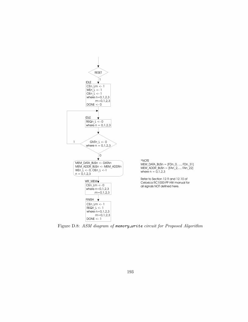
RESET
1IDLE
CE _L <- 1WE _L <- 1OE _L <- 1where =0,1,2,3
=0,1,2,3DONE <- 0
n m
n
n
n
m
REQ _L <- 0where = 0,1,2,3
n
n
IDLE
GNT _L <- 0where n = 0,1,2,3
n1
0
MEM_DATA_BUS <- DATAMEM_ADDR_BUS <- MEM_ADDRWE _L <- 0, OE _L <-1
= 0,1,2,3
n n
n n
n n
n
CE _L <- 0where =0,1,2,3
=0,1,2,3
n m
n
m
WR_MEM
FINISH
CE _L <- 1REQ _L <- 1where =0,1,2,3
=0,1,2,3DONE <- 1
n m
n
n
m
*NOTEMEM_DATA_BUSn = [FDn_0, ..., FDn_31]MEM_ADDR_BUSn = [FAn_2,..., FAn_22]where n = 0,1,2,3
Refer to Section 12.9 and 12.10 ofCeloxica RC1000-PP HW manual forall signals NOT defined here.
Figure D.8: ASM diagram of memory write circuit for Proposed Algorithm
193

PREP
MAR_OUT <- MEM_ADDRMCE_OUT <- 0
RESET
1INITDONE <- FALSEMAR_OUT <- 0MWRITE_OUT <- 1MREAD_OUT <- 1MCE_OUT <- 1MREQ_OUT <- 1\\MBX_ENABLE <- TRUE
REQMREQ_OUT <- 0
MOWN_OUT1
0
RW
TRUE FALSE
MWRITE_OUT <- 0 MREAD_OUT <- 0
DO
RW
TRUE FALSE
MWRITE_OUT <- 1 MREAD_OUT <- 1
FINMCE_OUT <- 1MREQ_OUT <- 1DONE <- 1
\\ MBX_ENABLE <- FALSE
Figure D.9: ASM diagram of Memory Controller (MemCont) unit
194
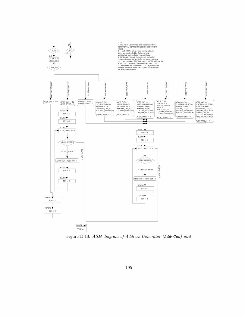
RESET
1IDLE
DONE <- 0RDY <- 0
CE
1
0
DATA_TYPE
Ne
uro
nW
gt (0
00
0)
Ne
uro
nBia
s (00
01
)
Ne
uro
nO
utp
ut (0
01
0)
Ne
uro
nErro
r (00
11
)
Inp
utPa
ttern
(01
00
)
Outp
utPa
ttern
(01
01
)
Outp
utE
rror (0
11
0)
Num
Ne
uro
ns (0
11
1)
Top
olo
gyD
ata
(10
00
)
ADDR_OUT <-<ERRADDR in Layer1>
+LAYER_CNT_IN*(3 + MAX_NEURONS)*CEIL(MAX_NEURONS/8)
ADDR_OFFSET <- 0
FOR NEURON0
ADDR_OUT <- TBDADDR_OFFSET<- 0
ADDR_OUT <- TBD
FINISH
DONE <- 1
(ADDR_OFFSET*8)
ADDR_OFFSET += 1
LOOP
<= MAX_LAYERS
ADDR_OUT = ADDR_OUT + 1
> M
AX
_LA
YERS
(ADDR_OFFSET*8)
LOOP
<= MAX_NEURONS
ADDR_OUT = ADDR_OUT + 1
> M
AX
_N
EU
RO
NS
ADDR_OFFSET += 1
ADDR_OUT <-<BIAS FOR NEURON0ADDR in LAYER1>+LAYER_CNT_IN*(3 + MAX_NEURONS)*CEIL(MAX_NEURONS/8)
ADDR_OFFSET <- 0
ADDR_OUT <-<WGT FOR NEURON0ADDR in LAYER1>+( NEURON_CNT_IN*
LAYER_CNT_IN*(3 + MAX_NEURONS)*CEIL(MAX_NEURONS/8)
ADDR_OFFSET <- 0
CEIL(MAX_NEURONS/8) )+
ADDR_OUT <-<OUTPUTNEURON0 ADDR inLayer1>+LAYER_CNT_IN*(3 + MAX_NEURONS)*CEIL(MAX_NEURONS/8)
ADDR_OFFSET <- 0
FORADDR_OUT <- TBDADDR_OFFSET <- 0
ADDR_OUT <-<INPUT TRAININGPATTERN0 ADDR>+PATTERN_CNT_IN*CEIL(MAX_NEURONS/8)
ADDR_OFFSET <- 0
ADDR_OUT <-<OUTPUT TRAININGPATTERN0 ADDR>+PATTERN_CNT_IN*CEIL(MAX_NEURONS/8)
ADDR_OFFSET <- 0
NOTE:1) TBD - To Be Determined (and is dependent onstatic memory architecture used for Feed-ForwardStage).2) <BASE ADDR> is base address of particulardata type as dictated by static memoryarchitecture used for Feed-Forward Stage.3) RDY (Ready) - Ready output is high for the firstclock cycle when the result of a generated addressbecomes available. ‘RDY’ indicates that ADDR_OUT is valid.4) Clock Enable input. CE enables the clock to theaddress generator, output and control registers in themodule. When CE is low, the clock may not changethe state of the module.
READY1
RDY <- 1
READY2
RDY <- 0
READY1
RDY <- 1
READY2
RDY <- 0
READY1
RDY <- 1
READY2
RDY <- 0
READY1
RDY <- 1
READY2
RDY <- 0
READY1
RDY <- 1
READY2
RDY <- 0
Figure D.10: ASM diagram of Address Generator (AddrGen) unit
195
Appendix E
Design Specifications for
RTR-MANN’s Backpropagation
Stage
E.1 Backpropagation Algorithm for Celoxica RC1000-PP
The control unit and datapath of RTR-MANN’s backpropagation stage was designed based
on the algorithm specified in this section. The following assumptions are made in order for
the Backpropagation algorithm to properly execute on the FPGA platform:
1. SoftCU has already pre-loaded Celoxica’s SRAM with correct data.
2. Feed-forward Stage has already run, and calculated error term(
ε(s)k
)
for output layer
(i.e. s = M).
3. SoftCU has already Reconfigured the Celoxica RC1000-PP with backpropagation
stage.
4. SoftCU has already reset circuit.
196

The following is a high-level description of the backpropagation algorithm, which was tar-
geted for execution on the Celoxica RC1000-PP:
1. Starting with the hidden layer closest to the output layer (i.e. s = (M − 1)) and
stepping backwards through the ANN one layer at a time:
• Calculate error term(
ε(s)k
)
for the kth neuron in the sth layer, according to Equa-
tions 2.9 and 2.10, using an adapted version of Eldredge’s Time-Multiplexed
Interconnection Scheme [15].
(a) First, in order to feed local gradient(
δ(s+1)j
)
values backwards, one of the
neurons (jth) in the (s + 1)th layer uses its existing error term(
ε(s+1)j
)
to
calculate its local gradient(
δ(s+1)j
)
, based on Equation 2.10 value is then
placed on the bus.
– Must initialize error term(
ε(s)k
)
for each neuron (kth) in the sth layer
equal to zero.
(b) All of the neurons in the sth layer read this value from the bus and multiply
it by the appropriate weight(
w(s+1)kj
)
storing the result.
(c) Then, the next neuron ((j+1)th) in the (s+1)th layer places its local gradient(
δ(s+1)(j+1)
)
on the bus.
(d) All of the kth neurons in the sth layer read this value and again multiply it(
δ(s+1)(j+1)
)
by the appropriate weight(
w(s+1)k(j+1)
)
value.
(e) The neurons in the sth layer then accumulate this product with the product
of the previous multiply.
(f) This process is repeated until all of the j th neurons in the (s+1)th layer have
had a chance to transfer their local gradients(
δ(s+1)j
)
to the kth neurons in
the sth layer.
The following is a more detailed pseudo-algorithm of how this backpropagation algorithm
would execute on the Celoxica platform:
197

1. Assumptions
Resetting the circuit results in the following:
• Sets all counters (e.g. layer counter, neuron counter, etc.) to zero
• Asserts reset signal of all neurons to logical ’1’
• Asserts reset signal of Memory Controller (MemCont) to ’1’
• Asserts reset signal of Address Generator (AddrGen) to ’1’
• Sets BACKPROP:DONE flag to logical ’0’
NOTE: SoftCU will not release ownership of memory until it has configured and
reset this circuit.
2. Execution
Retrieve the following from memory: Number of Non-Input Layers,
Current Training Pattern, Total Number Of Patterns, Max. neurons
in any given layer, and transfer this data to TOTAL_LAYERS,
pattern_counter, TOTAL_PATTERNS, and MAX_NEURON registers respectively.
Retrieve Number of Neurons for each layer, and transfer to
corresponding NUMNEURONSM register.
For (layer_counter= (TOTAL_LAYERS-1); j>=1; j--)
Determine Neurons in Layer (i.e. appropriate NUMNERONSM register
based on layer_counter)
Transfer Neuron Outputs to respective NEURON_OUTPUT registers
if(layer_counter == (TOTAL_LAYERS-1)) then
Retrieve the following from memory: Output Error
Transfer Error Term to respective ERROR_TERMM registers
198

End if;
Set DEFAULT_INPUT of all neuron entities to zero
Assert reset signal for each backprop_neuron entity, sets
output of entity equal to zero
Assert reset signal for LOCAL GRADIENT GENERATOR (i.e. multiplier)
For neuron_counter = i, where i = 0 to (Neurons in Layer+2)
//Allows 5-stage pipeline to finish
{
if(neuron_counter>=3)&&(neuron_counter<=Neurons in Layer + 2)
//if(neuron_counter > 2) needed to sync when local...
//...gradient arrives at Backprop Neuron
For each input neuron from previous layer
Retrieve the following from memory:Neuron Weight connected
to neuron in current layer (based on neuron_counter)
Transfer weight to respective WGT register
End for loop;
End if;
Do each of the following statements in parallel(i.e. like
separate threads in software):
if(neuron_counter>=0)&&(neuron_counter<=(Neurons in Layer-1))
Transfer NEURON_OUTPUTi to NeuronOutBus
End if;
If(neuron_counter>=1)&&(neuron_counter<=Neurons in Layer)
Transfer output of Derivative of Activation to input of
Local Gradient Generator
Transfer Error Term[i-1] to input of Local Gradient Generator
199
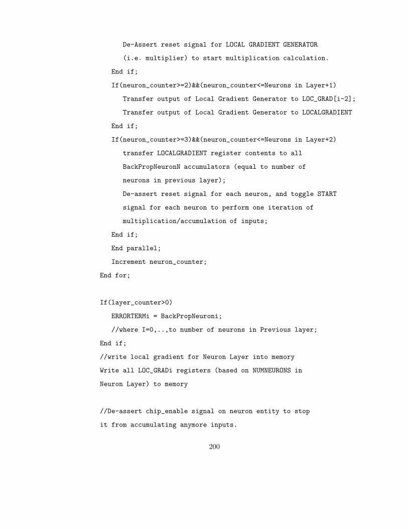
De-Assert reset signal for LOCAL GRADIENT GENERATOR
(i.e. multiplier) to start multiplication calculation.
End if;
If(neuron_counter>=2)&&(neuron_counter<=Neurons in Layer+1)
Transfer output of Local Gradient Generator to LOC_GRAD[i-2];
Transfer output of Local Gradient Generator to LOCALGRADIENT
End if;
If(neuron_counter>=3)&&(neuron_counter<=Neurons in Layer+2)
transfer LOCALGRADIENT register contents to all
BackPropNeuronN accumulators (equal to number of
neurons in previous layer);
De-assert reset signal for each neuron, and toggle START
signal for each neuron to perform one iteration of
multiplication/accumulation of inputs;
End if;
End parallel;
Increment neuron_counter;
End for;
If(layer_counter>0)
ERRORTERMi = BackPropNeuroni;
//where I=0,..,to number of neurons in Previous layer;
End if;
//write local gradient for Neuron Layer into memory
Write all LOC_GRADi registers (based on NUMNEURONS in
Neuron Layer) to memory
//De-assert chip_enable signal on neuron entity to stop
it from accumulating anymore inputs.
200
Increment layer_counter
End for;
Set DONE signal to logical 1, which notifies SoftCU that
processing is finished.
E.2 Backpropagation Algorithm’s Control Unit
The control unit created for RTR-MANN’s backpropagation stage of operation is called
backprop fsm, and was implemented as a finite state machine, and is based on the backprop
algorithm pseudo-code listed in Appendix E.1. Specification of the backprop fsm finite
state machine is given in the form of a ASM (Algorithmic State Machine) diagram, which
is partitioned up over Figures E.1- E.6.
E.3 Datapath for Feed-forward Algorithm
The datapath created for RTR-MANN’s backpropagation stage of operation was imple-
mented using the uog fixed arith 16-bit fixed-pt arithmetic library, and is based on the
backpropagation algorithm pseudo-code listed in Appendix E.1. Interface specifications,
ASM diagrams, and floorplans of the datapath logic units required for RTR-MANN’s back-
prop algorithm are provided in this section. Logic units that have been entirely derived
from one of the original uog fixed arith arithmetic units, such as ”BackProp Neuron”
and ”LOCAL GRADIENT GENERATOR” shown in Figure 5.9, will not be covered since the orig-
inal specifications of that particular arithmetic library are beyond the scope of this section.
Similarly, reused logic units that have already been defined for the feed-forward stage, such
as MemCont and AddrGen, will not be covered since specifications have already been made
201
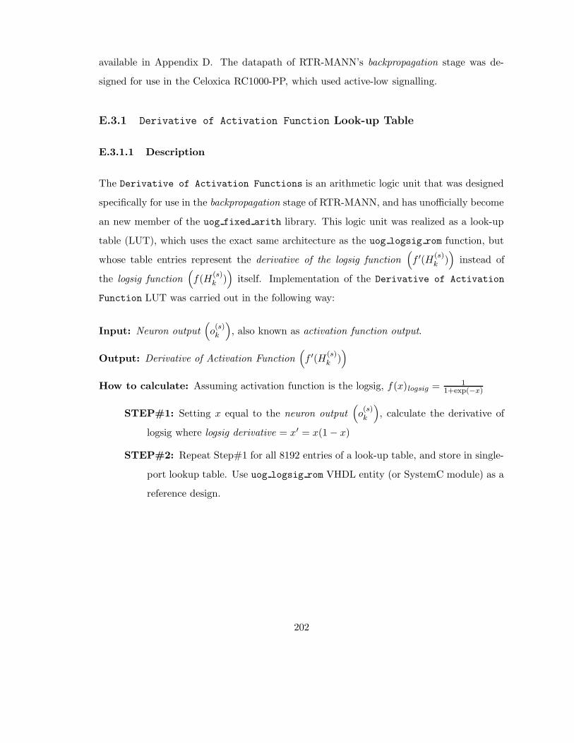
available in Appendix D. The datapath of RTR-MANN’s backpropagation stage was de-
signed for use in the Celoxica RC1000-PP, which used active-low signalling.
E.3.1 Derivative of Activation Function Look-up Table
E.3.1.1 Description
The Derivative of Activation Functions is an arithmetic logic unit that was designed
specifically for use in the backpropagation stage of RTR-MANN, and has unofficially become
an new member of the uog fixed arith library. This logic unit was realized as a look-up
table (LUT), which uses the exact same architecture as the uog logsig rom function, but
whose table entries represent the derivative of the logsig function(
f ′(H(s)k )
)
instead of
the logsig function(
f(H(s)k )
)
itself. Implementation of the Derivative of Activation
Function LUT was carried out in the following way:
Input: Neuron output(
o(s)k
)
, also known as activation function output.
Output: Derivative of Activation Function(
f ′(H(s)k )
)
How to calculate: Assuming activation function is the logsig, f(x)logsig = 11+exp(−x)
STEP#1: Setting x equal to the neuron output(
o(s)k
)
, calculate the derivative of
logsig where logsig derivative = x′ = x(1 − x)
STEP#2: Repeat Step#1 for all 8192 entries of a look-up table, and store in single-
port lookup table. Use uog logsig rom VHDL entity (or SystemC module) as a
reference design.
202

AddrGen:START<-0 AddrGen:RESET<-1
AddrGen:DATA_TYPE<-NumNeurons i:=0
BACKPROP_NN1
AddrGen:Reset <- 0
BACKPROP_NN2
AddrGen:DONE
RESET
LOCALGRADIENTGENERATOR:RESET<-1 DONE<- 0 layer_counter <-1 neuron_counter<-0 pattern_counter <-0 BackpropNeuron[0,...,N]:DEFAULT_OUT<-0
//where N=(MAX_NEURON-1) BackpropNeuralReset<-1 BackpropNeuron[0,..., N ]:Start<-0
//Ensures no continuous iteration of MAC calcs, //where N=max Neuron registers instantiated
AddrGen:START <- 0 //Ensures no false address offset is generated AddrGen:RESET <- 1 MemCont:RESET <- 1
BACKPROP_INIT
1
MBn:din <- "ZZZZZZZZZZZZZZZZ" ; n=0,...,7 //high impedance or floatingallows Celoxica RC1000 memory //to write to memory buffer registers (i.e. MBn)
AddrGen:DATA_TYPE <- TopologyData
BACKPROP_OTD1
BACKPROP_OTD2
AddrGen:RESET <- 0
AddrGen:DONE
BACKPROP_OTD3
MemCont:RW<-0 //read from memory
1
BACKPROP_OTD4
MemCont:RESET<-0
MemCont:DONE
0
BACKPROP_OTD5
MemCont:RESET<-1
BACKPROP_OTD6
layer_counter <- MB2:dout //TOTAL_LAYERS-1 pattern_counter := MB0:dout TOTAL_PATTERNS := MB1:dout TOTAL_LAYERS := (MB2:dout+1)//NON-INPUT LAYERS+1 MAX_NEURONS := MB3:dout AddrGen:MAX_LAYERS<-TOTAL_LAYERS AddrGen:MAX_PATTERNS<-TOTAL_PATTERNS AddrGen:MAX_NEURONS<-MAX_NEURONS AddrGen:PATT_CNT_IN<- pattern_counter AddrGen:LAYER_CNT_IN<-layer_counter AddrGen:NEURON_CNT_IN<-neuron_counter
1
0
AddrGen:OUT_OF_ RANGE
1
1 Go To BACKPROP_GET_NO1
MemCont:RW<-0 //read from memory
BACKPROP_NN3 0
BACKPROP_NN4
MemCont:RESET<-0
MemCont:DONE
0
1
If((n +8*i)<TOTAL_LAYERS) NUMNEURONS[n+8*i]<-MBn:dout // where n=0,...,7
BACKPROP_NN5
i:=i+1 AddrGen:START <- 1 MemCont:RESET <- 1
BACKPROP_NN6
AddrGen:START <- 0
BACKPROP_NN7
**NOTE: BACKPROP_OTD = Other Traning Data BACKPROP_NN = Number of Neurons (for each layer)
ASM diagrams with VHDL pseudo-code for BACKPROP_FSM module
0
Figure E.1: ASM diagram for backprop fsm control unit (Part 1 of 6)203
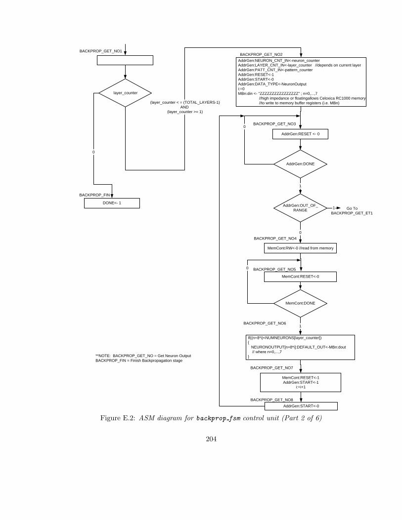
AddrGen:NEURON_CNT_IN<-neuron_counter AddrGen:LAYER_CNT_IN<-layer_counter //depends on current layer AddrGen:PATT_CNT_IN<-pattern_counter AddrGen:RESET<-1 AddrGen:START<-0 AddrGen:DATA_TYPE<-NeuronOutput i:=0 MBn:din <- "ZZZZZZZZZZZZZZZZ" ; n=0,...,7
//high impedance or floatingallows Celoxica RC1000 memory //to write to memory buffer registers (i.e. MBn)
BACKPROP_GET_NO2
BACKPROP_GET_NO3
AddrGen:RESET <- 0
AddrGen:DONE
BACKPROP_GET_NO4
MemCont:RW<-0 //read from memory
BACKPROP_GET_NO5
MemCont:RESET<-0
MemCont:DONE
0
BACKPROP_GET_NO6
MemCont:RESET<-1 AddrGen:START<-1
i:=i+1
BACKPROP_GET_NO7
If((n+8*i)<NUMNEURONS[layer_counter]) { NEURONOUTPUT[n+8*i]:DEFAULT_OUT<-MBn:dout // where n=0,...,7 }
1
AddrGen:OUT_OF_ RANGE
1
0
0
AddrGen:START<-0
BACKPROP_GET_NO8
BACKPROP_GET_NO1
layer_counter
BACKPROP_FIN
DONE<- 1
0
(layer_counter < = (TOTAL_LAYERS-1) AND
(layer_counter >= 1)
1 Go To BACKPROP_GET_ET1
**NOTE: BACKPROP_GET_NO = Get Neuron Output BACKPROP_FIN = Finish Backpropagation stage
Figure E.2: ASM diagram for backprop fsm control unit (Part 2 of 6)
204
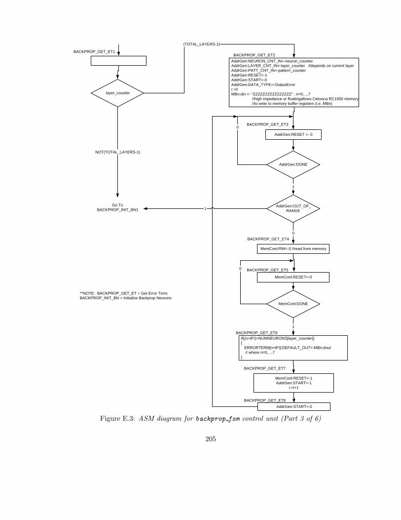
AddrGen:NEURON_CNT_IN<-neuron_counter AddrGen:LAYER_CNT_IN<-layer_counter //depends on current layer AddrGen:PATT_CNT_IN<-pattern_counter AddrGen:RESET<-1 AddrGen:START<-0 AddrGen:DATA_TYPE<-OutputError i:=0 MBn:din <- "ZZZZZZZZZZZZZZZZ" ; n=0,...,7
//high impedance or floatingallows Celoxica RC1000 memory //to write to memory buffer registers (i.e. MBn)
BACKPROP_GET_ET2
BACKPROP_GET_ET3
AddrGen:RESET <- 0
AddrGen:DONE
BACKPROP_GET_ET4
MemCont:RW<-0 //read from memory
BACKPROP_GET_ET5
MemCont:RESET<-0
MemCont:DONE
0
BACKPROP_GET_ET6
MemCont:RESET<-1 AddrGen:START<-1
i:=i+1
BACKPROP_GET_ET7
If((n+8*i)<NUMNEURONS[layer_counter]) { ERRORTERM[n+8*i]:DEFAULT_OUT<-MBn:dout // where n=0,...,7 }
1
AddrGen:OUT_OF_ RANGE
1
0
0
AddrGen:START<-0
BACKPROP_GET_ET8
BACKPROP_GET_ET1
layer_counter
NOT(TOTAL_LAYERS-1)
(TOTAL_LAYERS-1)
1 Go To
BACKPROP_INIT_BN1
**NOTE: BACKPROP_GET_ET = Get Error Term BACKPROP_INIT_BN = Initialize Backprop Neurons
Figure E.3: ASM diagram for backprop fsm control unit (Part 3 of 6)
205
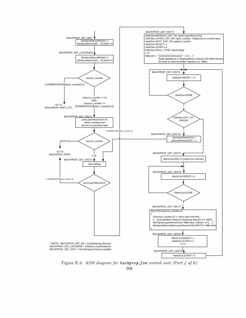
AddrGen:NEURON_CNT_IN<-(prevLayerNeuronCtr) AddrGen:LAYER_CNT_IN<-layer_counter //depends on current layer AddrGen:PATT_CNT_IN<-pattern_counter AddrGen:RESET<-1 AddrGen:START<-0 AddrGen:DATA_TYPE<-NeuronWgt i:=0 MBn:din <- "ZZZZZZZZZZZZZZZZ" ; n=0,...,7
//high impedance or floatingallows Celoxica RC1000 memory //to write to memory buffer registers (i.e. MBn)
BACKPROP_GET_WGT3
BACKPROP_GET_WGT4
AddrGen:RESET <- 0
AddrGen:DONE
BACKPROP_GET_WGT5
MemCont:RW<-0 //read from memory
BACKPROP_GET_WGT6
MemCont:RESET<-0
MemCont:DONE
0
BACKPROP_GET_WGT7
MemCont:RESET<-1 AddrGen:START<-1
i:=i+1
BACKPROP_GET_WGT8
If((n+8*i)<(neuron_counter-3) { //(neuron_counter-3) => don't start until first... //... local gradient ready for Backprop Neuron (i.e. MAC) WGT[prevLayerNeuronCtr]<-MBn:dout //where n=0,...,7 BackpropNeuron[prevLayerNeuronCtr]:INPUT2<-MBn:dout }
1
AddrGen:OUT_OF_ RANGE
1
0
0
AddrGen:START<-0
BACKPROP_GET_WGT9
BACKPROP_INIT_BN1 BackpropNeuralReset<-1
BackpropNeuron[0,...,N]:Start<-0
neuron_counter
(neuron_counter <= 0) AND
(neuron_counter <= (NUMNEURONS[layer_counter]+2))
1
BackpropNeuralReset<-1 BackpropNeuron[0,...,N]:Start<-0
BACKPROP_INIT_LOCGRAD1
(>NUMNEURONS[layer_counter]+2)
Go To BACKPROP_SHIFT_ET1
prevLayerNeuronCtr:=0 //start counting num
neurons in previous layer
BACKPROP_GET_WGT1
neuron_counter
//do nothing
(>2)
NOT(>2)
Go To BACKPROP_PIPE1
BACKPROP_GET_WGT2
prevLayerNeuronCtr
(>=NUMNEURON[layer_counter-1])
(<NUMNEURON[layer_counter-1])
perLayerNeuronCtr:= perLayerNeuronCtr + 1
BACKPROP_GET_WGT10
**NOTE: BACKPROP_INIT_BN = Init Backprop Neurons BACKPROP_INIT_LOCGRAD = Initialize LocalGradients BACKPROP_GET_WGT = Get Backprop Neuron weights
Figure E.4: ASM diagram for backprop fsm control unit (Part 4 of 6)
206
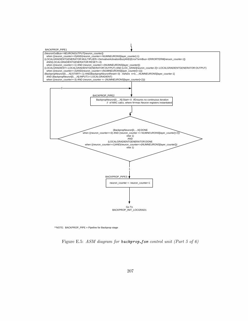
(NeuronOutBus<-NEURONOUTPUT[neuron_counter]) when ((neuron_counter>=0)AND(neuron_counter<=NUMNEURONS[layer_counter]-1) (LOCALGRADIENTGENERATOR:MULTIPLIER<-DerivativeActivationBus)AND(ErrorTermBus<-ERRORTERM[neruon_counter-1]) AND(LOCALGRADIENTGENERATOR:RESET<-0) when ((neuron_counter>=1) AND (neuron_counter<=(NUMNEURONS[layer_counter])) (LOCALGRADIENT<-LOCALGRADIENTGENERATOR:OUTPUT) AND (LOC_GRAD[neuron_counter-2]<-LOCALGRADIENTGENERATOR:OUTPUT) when ((neuron_counter>=2)AND(neuron_counter<=(NUMNEURONS[layer_counter]+1))) (BackpropNeuron[0,...,N]:START<-1) AND(BackpropNeuronReset<-0) //where n=0,...,NUMNEURONS[layer_counter-1] AND (BackpropNeuron[0,...,N]:INPUT1<-LOCALGRADIENT) when ((neuron_counter>=3) AND (neuron_counter <= (NUMNEURONS[layer_counter]+2)))
BACKPROP_PIPE1
BackpropNeuron[0,...,N]:Start<-0 //Ensures no continuous iteration // of MAC calcs, where N=max Neuron registers instantiated
BACKPROP_PIPE2
(BackpropNeuron[0,...,N]:DONE when ((neuron_counter>=3) AND (neuron_counter <= NUMNEURONS[layer_counter]+2))
else 1) AND
(LOCALGRADIENTGENERATOR:DONE when ((neuron_counter>=1)AND(neuron_counter<=(NUMNEURONS[layer_counter]))
else 1)
0
Go To BACKPROP_INIT_LOCGRAD1
1
neuron_counter <- neuron_counter+1
BACKPROP_PIPE3
**NOTE: BACKPROP_PIPE = Pipeline for Backprop stage
Figure E.5: ASM diagram for backprop fsm control unit (Part 5 of 6)
207
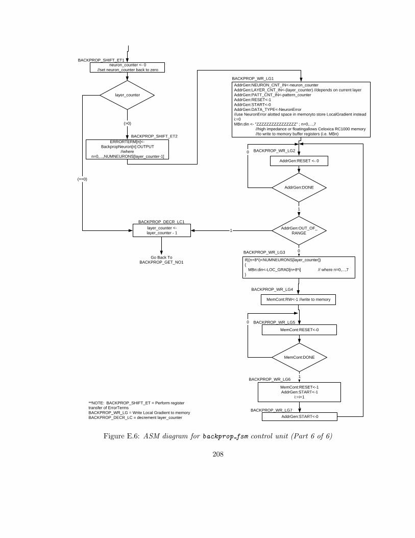
AddrGen:NEURON_CNT_IN<-neuron_counter AddrGen:LAYER_CNT_IN<-(layer_counter) //depends on current layer AddrGen:PATT_CNT_IN<-pattern_counter AddrGen:RESET<-1 AddrGen:START<-0 AddrGen:DATA_TYPE<-NeuronError //use NeuronError alotted space in memoryto store LocalGradient instead i:=0 MBn:din <- "ZZZZZZZZZZZZZZZZ" ; n=0,...,7
//high impedance or floatingallows Celoxica RC1000 memory //to write to memory buffer registers (i.e. MBn)
BACKPROP_WR_LG1
BACKPROP_WR_LG2
AddrGen:RESET <- 0
AddrGen:DONE
BACKPROP_WR_LG4
MemCont:RW<-1 //write to memory
BACKPROP_WR_LG5
MemCont:RESET<-0
MemCont:DONE
0
BACKPROP_WR_LG3
MemCont:RESET<-1 AddrGen:START<-1
i:=i+1
BACKPROP_WR_LG6
If((n+8*i)<NUMNEURONS[layer_counter]) { MBn:din<-LOC_GRAD[n+8*i] // where n=0,...,7 }
1
0
AddrGen:OUT_OF_ RANGE
1
0
AddrGen:START<-0
BACKPROP_WR_LG7
BACKPROP_SHIFT_ET1 neuron_counter <- 0
//set neuron_counter back to zero
layer_counter
ERRORTERM[n]<- BackpropNeuron[n]:OUTPUT
//where n=0,...,NUMNEURONS[layer_counter-1]
BACKPROP_SHIFT_ET2
(>0)
1
(==0)
layer_counter <- layer_counter - 1
BACKPROP_DECR_LC1
Go Back To BACKPROP_GET_NO1
**NOTE: BACKPROP_SHIFT_ET = Perform register transfer of ErrorTerms BACKPROP_WR_LG = Write Local Gradient to memory BACKPROP_DECR_LC = decrement layer_counter
Figure E.6: ASM diagram for backprop fsm control unit (Part 6 of 6)
208

Appendix F
Design Specifications for
RTR-MANN’s Weight Update
Stage
F.1 Weight Update Algorithm for Celoxica RC1000-PP
The control unit and datapath of RTR-MANN’s weight update stage was designed based
on the algorithm specified in this section. The following assumptions are made in order for
the Weight Update algorithm to properly execute on the FPGA platform:
1. SoftCU has already pre-loaded Celoxica’s SRAM with correct data.
2. Feed-forward Stage has already run
3. Backpropagation Stage has already run, and calculated local gradient associated with
each neuron.
4. SoftCU has already Reconfigured the Celoxica RC1000-PP with Weight Update stage.
5. SoftCU has already reset this circuit.
209

The following is a high-level description of the Weight Update algorithm, which was targeted
for execution on the Celoxica RC1000-PP:
1. Starting with the hidden layer closest to the output layer (i.e. s = (M − 1)) and
stepping backwards through the ANN one layer at a time:
• Calculate change in synaptic weight (or bias) ∆w(s+1)kj corresponding to the gra-
dient of error for connection from neuron unit j in the (s)th layer, to neuron k
in the (s+1)th layer. This calculation is done in accordance with Equation 2.12.
• Calculate the updated synaptic weight (or bias) w(s+1)kj (n + 1) to be used in the
next Feed-Forward stage, according to Equation 2.13.
The following is a more detailed pseudo-algorithm of how this backpropagation algorithm
would execute on the Celoxica platform:
1. Assumptions
Resetting the circuit results in the following:
• Sets all counters (e.g. layer counter, neuron counter, etc.) to zero
• Asserts reset signal of all neurons to logical ’1’
• Asserts reset signal of Memory Controller (MemCont) to ’1’
• Asserts reset signal of Address Generator (AddrGen) to ’1’
• Sets WGT UPDATE:DONE flag to logical ’0’
NOTE: SoftCU will not release ownership of memory until it has configured and
reset this circuit.
2. Execution
Retrieve the following from memory: Number of Non-Input Layers,
Current Training Pattern, Total Number Of Patterns, Max. neurons
in any given layer, learning rate and transfer this data to
210
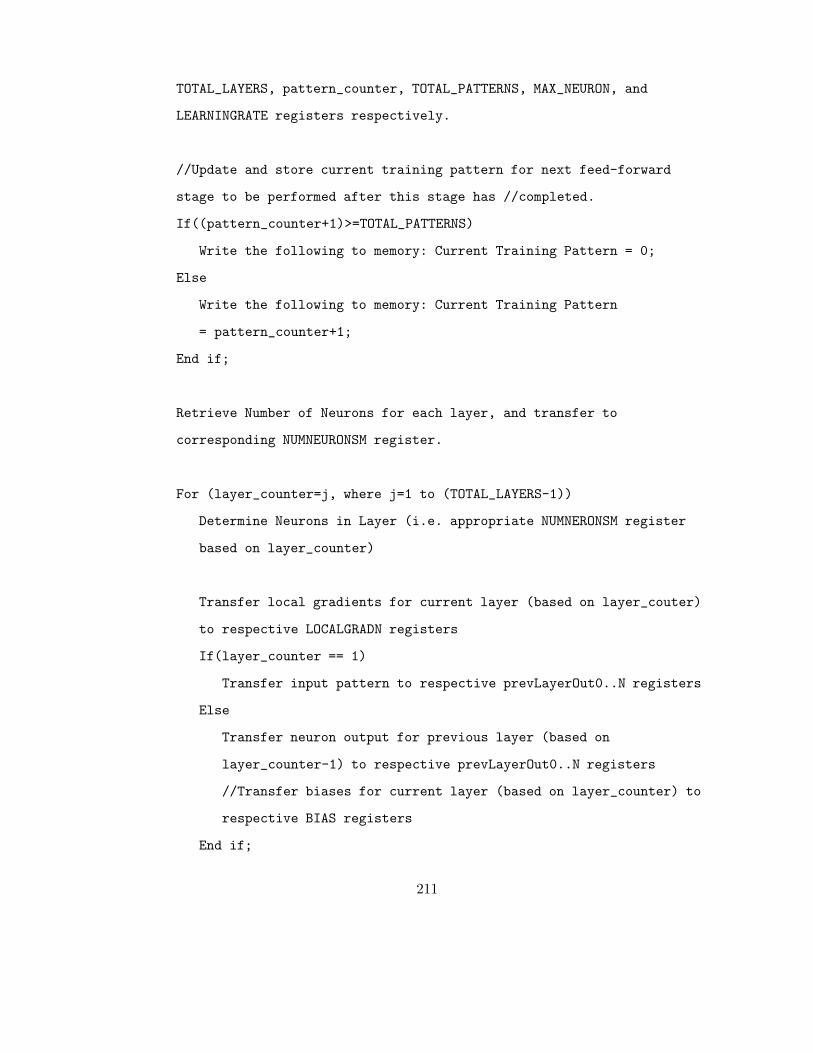
TOTAL_LAYERS, pattern_counter, TOTAL_PATTERNS, MAX_NEURON, and
LEARNINGRATE registers respectively.
//Update and store current training pattern for next feed-forward
stage to be performed after this stage has //completed.
If((pattern_counter+1)>=TOTAL_PATTERNS)
Write the following to memory: Current Training Pattern = 0;
Else
Write the following to memory: Current Training Pattern
= pattern_counter+1;
End if;
Retrieve Number of Neurons for each layer, and transfer to
corresponding NUMNEURONSM register.
For (layer_counter=j, where j=1 to (TOTAL_LAYERS-1))
Determine Neurons in Layer (i.e. appropriate NUMNERONSM register
based on layer_counter)
Transfer local gradients for current layer (based on layer_couter)
to respective LOCALGRADN registers
If(layer_counter == 1)
Transfer input pattern to respective prevLayerOut0..N registers
Else
Transfer neuron output for previous layer (based on
layer_counter-1) to respective prevLayerOut0..N registers
//Transfer biases for current layer (based on layer_counter) to
respective BIAS registers
End if;
211
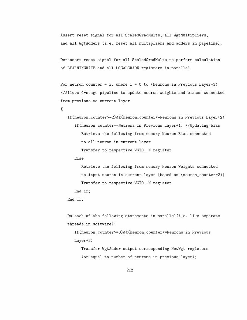
Assert reset signal for all ScaledGradMults, all WgtMultipliers,
and all WgtAdders (i.e. reset all multipliers and adders in pipeline).
De-assert reset signal for all ScaledGradMults to perform calculation
of LEARNINGRATE and all LOCALGRADN registers in parallel.
For neuron_counter = i, where i = 0 to (Neurons in Previous Layer+3)
//Allows 4-stage pipeline to update neuron weights and biases connected
from previous to current layer.
{
If(neuron_counter>=2)&&(neuron_counter<=Neurons in Previous Layer+2)
if(neuron_counter==Neurons in Previous Layer+1) //Updating bias
Retrieve the following from memory:Neuron Bias connected
to all neuron in current layer
Transfer to respective WGT0..N register
Else
Retrieve the following from memory:Neuron Weights connected
to input neuron in current layer [based on (neuron_counter-2)]
Transfer to respective WGT0..N register
End if;
End if;
Do each of the following statements in parallel(i.e. like separate
threads in software):
If(neuron_counter>=3)&&(neuron_counter<=Neurons in Previous
Layer+3)
Transfer WgtAdder output corresponding NewWgt registers
(or equal to number of neurons in previous layer);
212
End if;
If(neuron_counter>=2)&&(neuron_counter<=Neurons in Previous
Layer+2)
Transfer WgtMultiplier output corresponding WgtAdder
input (or equal to number of neurons in previous layer);
Transfer WGT registers to corresponding WgtAdder input
(or equal to number of neurons in previous layer);
De-assert reset signal for all WgtAdder (i.e. adders)
End if;
If(neuron_counter>=1)&&(neuron_counter<=Neurons in Previous
Layer+1)
Transfer PrevLayerOutput register to all WgtMultiplier
inputs (or equal to number of neurons in previous layer);
De-Assert reset signal for WgtMultiplier0..N
(i.e. multiplier) to start multiplication calculation.
End if;
Assert reset signal for WgtMultiplier0..N (i.e. multiplier) to
prepare for next multiplication calculation in pipeline.
if(neuron_counter>=0)&&(neuron_counter<=(Neurons in Previous
Layer))
if(neuron_counter==Neurons in Previous Layer)
//if updating bias
prevLayerOutput=1;
else
Transfer prevLayerOut[neuron_counter] to prevLayerOutput
(input signal of WgtMultiplier0..N)
//output signal of ScaledGrandMult0..N already initialized
end if;
213
End if;
End parallel;
//Write results to memory
If(neuron_counter>=3)&&(neuron_counter<=Neurons in Previous
Layer+3)
if(neuron_counter==Neurons in Previous Layer+3)
//if updating bias
Write the following to memory: NewWgt to corresponding
NeuronBias
memory (equal to number of neurons in previous layer);
Else
Write the following to memory: NewWgt to corresponding
NeuronWgt
memory (equal to number of neurons in previous layer);
End if;
End If;
Increment neuron_counter;
End for;
Increment layer_counter;
End for;
Set DONE signal to logical 1, which notifies SoftCU that processing
is finished.
214
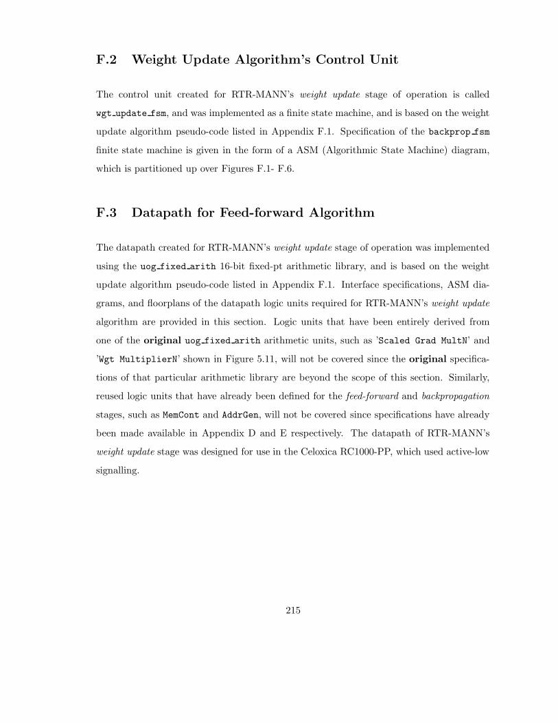
F.2 Weight Update Algorithm’s Control Unit
The control unit created for RTR-MANN’s weight update stage of operation is called
wgt update fsm, and was implemented as a finite state machine, and is based on the weight
update algorithm pseudo-code listed in Appendix F.1. Specification of the backprop fsm
finite state machine is given in the form of a ASM (Algorithmic State Machine) diagram,
which is partitioned up over Figures F.1- F.6.
F.3 Datapath for Feed-forward Algorithm
The datapath created for RTR-MANN’s weight update stage of operation was implemented
using the uog fixed arith 16-bit fixed-pt arithmetic library, and is based on the weight
update algorithm pseudo-code listed in Appendix F.1. Interface specifications, ASM dia-
grams, and floorplans of the datapath logic units required for RTR-MANN’s weight update
algorithm are provided in this section. Logic units that have been entirely derived from
one of the original uog fixed arith arithmetic units, such as ’Scaled Grad MultN’ and
’Wgt MultiplierN’ shown in Figure 5.11, will not be covered since the original specifica-
tions of that particular arithmetic library are beyond the scope of this section. Similarly,
reused logic units that have already been defined for the feed-forward and backpropagation
stages, such as MemCont and AddrGen, will not be covered since specifications have already
been made available in Appendix D and E respectively. The datapath of RTR-MANN’s
weight update stage was designed for use in the Celoxica RC1000-PP, which used active-low
signalling.
215
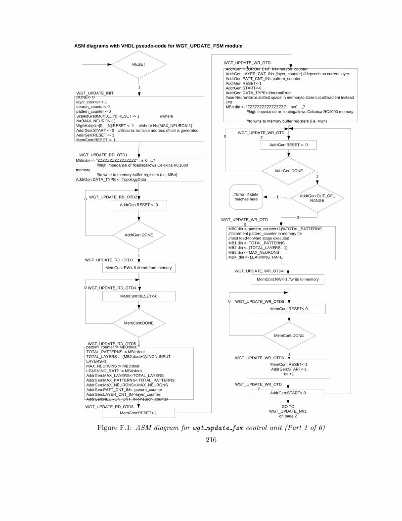
ASM diagrams with VHDL pseudo-code for WGT_UPDATE_FSM module
RESET
DONE<- 0 layer_counter <-1 neuron_counter<-0 pattern_counter <-0 ScaledGradMult[0,...,N]:RESET <- 1 //where N=(MAX_NEURON-1) WgtMultiplier[0,...,N]:RESET <- 1 //where N=(MAX_NEURON-1) AddrGen:START <- 0 //Ensures no false address offset is generated AddrGen:RESET <- 1 MemCont:RESET <- 1
WGT_UPDATE_INIT
1
MBn:din <- "ZZZZZZZZZZZZZZZZ" ; n=0,...,7 //high impedance or floatingallows Celoxica RC1000
memory //to write to memory buffer registers (i.e. MBn)
AddrGen:DATA_TYPE <- TopologyData
WGT_UPDATE_RD_OTD1
WGT_UPDATE_RD_OTD2
AddrGen:RESET <- 0
AddrGen:DONE
WGT_UPDATE_RD_OTD3
MemCont:RW<-0 //read from memory
1
WGT_UPDATE_RD_OTD4
MemCont:RESET<-0
MemCont:DONE
0
WGT_UPDATE_RD_OTD5
MemCont:RESET<-1
WGT_UPDATE_RD_OTD6
pattern_counter := MB0:dout TOTAL_PATTERNS := MB1:dout TOTAL_LAYERS := (MB2:dout+1)//NON-INPUT LAYERS+1 MAX_NEURONS := MB3:dout LEARNING_RATE := MB4:dout AddrGen:MAX_LAYERS<-TOTAL_LAYERS AddrGen:MAX_PATTERNS<-TOTAL_PATTERNS AddrGen:MAX_NEURONS<-MAX_NEURONS AddrGen:PATT_CNT_IN<- pattern_counter AddrGen:LAYER_CNT_IN<-layer_counter AddrGen:NEURON_CNT_IN<-neuron_counter
1
0
AddrGen:NEURON_CNT_IN<-neuron_counter AddrGen:LAYER_CNT_IN<-(layer_counter) //depends on current layer AddrGen:PATT_CNT_IN<-pattern_counter AddrGen:RESET<-1 AddrGen:START<-0 AddrGen:DATA_TYPE<-NeuronError //use NeuronError alotted space in memoryto store LocalGradient instead i:=0 MBn:din <- "ZZZZZZZZZZZZZZZZ" ; n=0,...,7
//high impedance or floatingallows Celoxica RC1000 memory
//to write to memory buffer registers (i.e. MBn)
WGT_UPDATE_WR_OTD 1
WGT_UPDATE_WR_OTD 2
AddrGen:RESET <- 0
AddrGen:DONE
WGT_UPDATE_WR_OTD4
MemCont:RW<-1 //write to memory
WGT_UPDATE_WR_OTD5
MemCont:RESET<-0
MemCont:DONE
0
WGT_UPDATE_WR_OTD 3
MemCont:RESET<-1 AddrGen:START<-1
i:=i+1
WGT_UPDATE_WR_OTD6
MB0:din <- pattern_counter+1)%TOTAL_PATTERNS //increment pattern_counter in memory for //next feed-forward stage executed MB1:din <- TOTAL_PATTERNS MB2:din <- (TOTAL_LAYERS - 1) MB3:din <- MAX_NEURONS MB4_din <- LEARNING_RATE
1
0
AddrGen:OUT_OF_ RANGE
1
0
AddrGen:START<-0
WGT_UPDATE_WR_OTD 7
GO TO WGT_UPDATE_NN1
on page 2
//Error if state reaches here
1
Figure F.1: ASM diagram for wgt update fsm control unit (Part 1 of 6)
216

AddrGen:START<-0 AddrGen:RESET<-1 AddrGen:DATA_TYPE <- NumNeurons i := 0 MBn:din <- "ZZZZZZZZZZZZZZZZ" ; n=0,...,7
//high impedance or floatingallows Celoxica RC1000 memory
//to write to memory buffer registers (i.e. MBn)
WGT_UPDATE_NN1
WGT_UPDATE_NN2
AddrGen:RESET <- 0
AddrGen:DONE
WGT_UPDATE_NN3
MemCont:RW<-0 //read from memory
0
WGT_UPDATE_NN4
MemCont:RESET<-0
MemCont:DONE
0
WGT_UPDATE_NN5
i:= i+1 AddrGen:START <- 1 MemCont:RESET <- 1
WGT_UPDATE_NN6
If( (n+8*i) < TOTAL_LAYERS) { NUMNEURONS[n+8*i] <- MBn:dout //where n=0,...,7 }
1
0
AddrGen:OUT_OF_ RANGE
1
AddrGen:START <- 0
WGT_UPDATE_NN7
//do nothing WGT_UPDATE_LAYER_LOOP
AddrGen:DONE
WGT_UPDATE_FIN
DONE <- 1 (>=
TOTAL_LAYERS)
AddrGen:START<-0 AddrGen:RESET<-1 AddrGen:DATA_TYPE <- NeuronError //NeuronError type memory storage utilized for Local Gradient instead i := 0 MBn:din <- "ZZZZZZZZZZZZZZZZ" ; n=0,...,7 //high impedance or floatingallows Celoxica
//RC1000 memory to write to memory buffer registers (i.e. MBn) AddrGen:NEURON_CNT_IN <- neuron_counter AddrGen:LAYER_CNT_IN <- layer_counter //depends on current layer AddrGen:PATT_CNT_IN <- pattern_counter
WGT_UPDATE_LOCGRAD1
WGT_UPDATE_LOCGRAD2
AddrGen:RESET <- 0
AddrGen:DONE
WGT_UPDATE_LOCGRAD3
MemCont:RW<-0 //read from memory
0
WGT_UPDATE_LOCGRAD4
MemCont:RESET<-0
MemCont:DONE
0
WGT_UPDATE_LOCGRAD5
i:= i+1 AddrGen:START <- 1 MemCont:RESET <- 1
WGT_UPDATE_LOCGRAD6
If( (n+8*i) < NUMNEURONS[layer_counter]) { LOCALGRAD[n+8*i] <- MBn:dout //where n=0,...,7 }
1
0
AddrGen:OUT_OF_ RANGE
1
AddrGen:START <- 0
WGT_UPDATE_LOCGRAD7
1
Go To WGT_UPDATE_PREVLAYEROUT
on page 3
Figure F.2: ASM diagram for wgt update fsm control unit (Part 2 of 6)217

AddrGen:START<-0 AddrGen:RESET<-1 (AddrGen:DATA_TYPE <- InputPattern) AND (AddrGen:LAYER_CNT_IN <- layer_counter) when (layer_counter == 1) else (AdrGen:DATA_TYPE <- NeuronOutput) AND (AddrGen:LAYER_CNT_IN <- layer_counter-1) i := 0 MBn:din <- "ZZZZZZZZZZZZZZZZ" ; n=0,...,7
//high impedance or floatingallows Celoxica RC1000 memory
//to write to memory buffer registers (i.e. MBn) AddrGen:NEURON_CNT_IN <- neuron_counter AddrGen:PATT_CNT_IN <- pattern_counter
WGT_UPDATE_PREVLAYEROUT1
WGT_UPDATE_PREVLAYEROUT2
AddrGen:RESET <- 0
AddrGen:DONE
WGT_UPDATE_PREVLAYEROUT3
MemCont:RW<-0 //read from memory
0
WGT_UPDATE_PREVLAYEROUT4
MemCont:RESET<-0
MemCont:DONE
0
WGT_UPDATE_PREVLAYEROUT5
i:= i+1 AddrGen:START <- 1 MemCont:RESET <- 1
WGT_UPDATE_PREVLAYEROUT6
If( (n+8*i) < NUMNEURONS[layer_counter-1]) { //depends on previous layer prevLayerOut[n+8*i] <- MBn:dout //where n=0,...,7 }
1
0
AddrGen:OUT_OF_ RANGE
1
AddrGen:START <- 0
WGT_UPDATE_PREVLAYEROUT7
Go To WGT_UPDATE_SCALED1
on page 4
Figure F.3: ASM diagram for wgt update fsm control unit (Part 3 of 6)218

WGT_UPDATE_SCALED1
ScaledGradMult[0,...,N]:RESET <- 1 WgtMultiplier[0,...,N]:RESET <- 1
WgtAdder[0,...,N]:RESET <- 1 //where N+1 = (MAX_NEURON-1)
WGT_UPDATE_SCALED2
ScaledGradMult[0,...,N]:RESET<-0
ScaledGradMult[0,...,N]: DONE
0
WGT_UPDATE_SCALED3
//do nothing
WGT_UPDATE_NEURON_LOOP
neuron_counter <- 0
1
neuron_counte r
neuron_counte r
(> NUMNEURONS [layer_counter-
1]+3)
(<= NUMNEURONS [layer_counter-1]+3
Go
To
WG
T_U
PD
AT
_LA
YE
R_I
NC
R
on p
age
??
((neuron_counter >= 2) AND (neuron_counter <=
NUMNEURONS[layer_counter- 1]+2))
NOT((neuron_counter >= 2) AND (neuron_counter <=
NUMNEURONS[layer_counter- 1]+2))
Go To WGT_UPDATE_PIPE1
on page ??
AddrGen:START<-0 AddrGen:RESET<-1 (AddrGen:DATA_TYPE <- NeuronBias) when (neuron_counter == NUMNEURONS[layer_counter-1]+2) else (AddrGen:DATA_TYPE <- NeuronWgt) i := 0 MBn:din <- "ZZZZZZZZZZZZZZZZ" ; n=0,...,7
//high impedance or floatingallows Celoxica RC1000 memory
//to write to memory buffer registers (i.e. MBn) AddrGen:NEURON_CNT_IN <- (neuron_counter - 2) //depends on (neuron_counter -2) due to delay in pipeline AddrGen:LAYER_CNT_IN <- layer_counter AddrGen:PATT_CNT_IN <- pattern_counter
WGT_UPDATE_RD_WGT1
WGT_UPDATE_RD_WGT2
AddrGen:RESET <- 0
AddrGen:DONE
WGT_UPDATE_RD_WGT3
MemCont:RW<-0 //read from memory
0
WGT_UPDATE_RD_WGT4
MemCont:RESET<-0
MemCont:DONE
0
WGT_UPDATE_RD_WGT5
i:= i+1 AddrGen:START <- 1 MemCont:RESET <- 1
WGT_UPDATE_RD_WGT6
If( (n+8*i) < NUMNEURONS[layer_counter]) { //depends on current layer WGT[n+8*i] <- MBn:dout //where n=0,...,7 }
1
0
AddrGen:OUT_OF_ RANGE
1
AddrGen:START <- 0
WGT_UPDATE_RD_WGT7
Go To WGT_UPDATE_PIPE1
on page ??
Figure F.4: ASM diagram for wgt update fsm control unit (Part 4 of 6)219
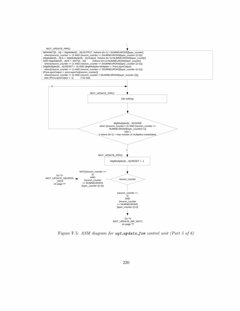
NEWWGT[0,..,N] <- WgtAdder[0,..,N]:OUTPUT //where (N+1) = NUMNEURONS[layer_counter] when((neuron_counter >= 3) AND (neuron_counter <= (NUMNEURONS[layer_counter-1]+3))) (WgtAdder[0,..,N]:A <- WgtMultiplier[0,..,N]:Output) //where (N+1)=NUMNEURONS[layer_counter] AND (WgtAdder[0,..,N]:B <- WGT[0,..,N]) //where (N+1)=NUMNEURONS[layer_counter] when((neuron_counter >= 2) AND (neuron_counter <= (NUMNEURONS[layer_counter-1]+2))) (WgtMultiplier[0,..,N]:RESET <- 0) AND (WgtMultiplier:Multiplier <- PrevLayerOutput) when((neuron_counter >= 1) AND (neuron_counter <= (NUMNEURONS[layer_counter-1]+1))) (PrevLayerOutput <- prevLayerOut[neuron_counter]) when((neuron_counter >= 0) AND (neuron_counter < (NUMNEURONS[layer_counter-1]))) else (PrevLayerOutput <- 1) // for bias
WGT_UPDATE_PIPE1
//do nothing
WGT_UPDATE_PIPE2
WgtMultiplier[0,..,N]:DONE when ((neuron_counter>=1) AND (neuron_counter <=
NUMNEURONS[layer_counter]+1)) else 1
// where (N+1) = max number of multipliers instantiated
0
1
WgtMultiplier[0,..,N]:RESET <- 1
WGT_UPDATE_PIPE3
neuron_counter
(neuron_counter >= 3)
AND (neuron_counter
<= NUMNEURONS [layer_counter-1]+3)
NOT((neuron_counter >= 3)
AND (neuron_counter
<= NUMNEURONS [layer_counter-1]+3))
Go To WGT_UPDATE_NEURON
_INCR on page ??
Go To WGT_UPDATE_WR_WGT1
on page ??
Figure F.5: ASM diagram for wgt update fsm control unit (Part 5 of 6)
220

AddrGen:NEURON_CNT_IN<-(neuron_counter-3) //sync with pipeline AddrGen:LAYER_CNT_IN<-(layer_counter) //depends on current layer AddrGen:PATT_CNT_IN<-pattern_counter AddrGen:RESET<-1 AddrGen:START<-0 AddrGen:DATA_TYPE<-NeuronWgt when ((neuron_counter >= 3) AND (neuron_counter <= (NUMNEURONS[layer_counter-1]+2))) else (AddrGen:DATA_TYPE <- (NUMNEURONS[layer_counter-1]+2)) i:=0 MBn:din <- "ZZZZZZZZZZZZZZZZ" ; n=0,...,7
//high impedance or floatingallows Celoxica RC1000 memory
//to write to memory buffer registers (i.e. MBn)
WGT_UPDATE_WR_WGT1
WGT_UPDATE_WR_WGT2
AddrGen:RESET <- 0
AddrGen:DONE
WGT_UPDATE_WR_WGT4
MemCont:RW<-1 //write to memory
WGT_UPDATE_WR_WGT5
MemCont:RESET<-0
MemCont:DONE
0
WGT_UPDATE_WR_WGT 3
MemCont:RESET<-1 AddrGen:START<-1
i:=i+1
WGT_UPDATE_WR_WGT6
If((n+8*i)<NUMNEURONS[layer_counter]) { MBn:din<-NEWWGT[n+8*i] // where n=0,...,7 }
1
0
AddrGen:OUT_OF_ RANGE
1
0
AddrGen:START<-0
WGT_UPDATE_WR_WGT7
neuron_counter <- neuron_counter + 1
WGT_UPDATE_NEURON_INCR
Go Back To WGT_UPDATE_NEURON
_LOOP on page ??
layer_counter <- layer_counter + 1
WGT_UPDATE_LAYER_INCR
Go Back To WGT_UPDATE_LAYER_INCR
on page ??
Figure F.6: ASM diagram for wgt update fsm control unit (Part 6 of 6)
221
Related Documents