A Racetrack Memory Based In-memory Booth Multiplier for Cryptography Application Tao Luo 1 , Wei Zhang 2 , Bingsheng He 1 and Douglas Maskell 1 1 School of Computer Engineering, Nanyang Technological University, Singapore 2 Department of Electronic & Computer Engineering, Hong Kong University of Science and Technology, Hong Kong Abstract— Security is an important concern in cloud comput- ing nowadays. RSA is one of the most popular asymmetric en- cryption algorithms that are widely used in internet based appli- cations for its public key strategy advantage over symmetric en- cryption algorithms. However, RSA encryption algorithm is very compute intensive, which would affect the speed and power effi- ciency of the encountered applications. Racetrack Memory (RM) is a newly introduced promising technology in future storage and memory system, which is perfect to be used in memory intensive scenarios because of its high data density. However, novel designs should be applied to exploit the advantages of RM while avoid- ing the adverse impact of its sequential access mechanism. In this paper, we present an in-memory Booth multiplier based on race- track memory to alleviate this problem. As the building block of our multiplier, a racetrack memory based adder is proposed, which saves 56.3% power compared with the state-of-the-art mag- netic adder. Integrated with the storage element, our proposed multiplier shows great efficiency in area, power and scalability. I. I NTRODUCTION With the development of information technology, we are en- tering the big data era, where large amount of data need to be created, processed and transferred in the cloud, which imposes high requirement on the security. RSA is one of the most pop- ular asymmetric encryption algorithms that are widely adopted by internet based applications [1]. Asymmetric encryption is more suitable and efficient than symmetric encryption because that its public key strategy well solves the difficulty of key ex- change existed in symmetric encryption systems. However, the encryption and decryption operations in the RSA scheme in- volve massive exponentiation, which makes the RSA encryp- tion scheme time and resource consuming. Besides, the in- creasing key length (more than 521 bits) required to ensure the security level makes the problem more severe. Racetrack memory is a newly introduced memory technol- ogy that has the advantages of high density, non-volatility, low power and high speed [2]. It is a promising technology that not only can be used in all hierarchy of memory system from exter- nal storage to main memory, but also has the capability as in- memory computing for logic design. Since racetrack memory has great potential to be used as data storage in data center, in order to accelerate the encryption and decryption of the stored data, in this work, we present the first design of a racetrack memory based in-memory Booth multiplier for RSA cryptog- raphy applications. With the in-memory encryption, firstly, it avoids the efforts for shifting the target data to the access port due to the sequential access mechanism of racetrack memory. Secondly, the I/O requirement is significantly reduced because there is no need to transfer the data between the memory and processor just for encryption. The basic operation of RSA is multiplication, which is also the fundamental arithmetic operation in various kinds of data intensive applications such as compression, image processing, etc. Hence, our racetrack multiplier design could be general and applicable to many in-memory computing applications. We choose to implement a Booth multiplier since it is one of the most efficient multiplication algorithms for binary digit multi- plication. We first present a racetrack memory based adder as the building block of the multiplier and then develop the multi- plier through an efficient connection of the adders. Compared with previous magnetic adder design, our adder saves 66% of area and 56.3% of power [3]. The key contributions of this work can be summarized as: 1. A compact racetrack memory based adder is proposed to optimize the area and power of the basic addition opera- tion. 2. The Booth decoder and encoder are designed for the pro- posed Booth multiplier to exploit the inherent sequential access mechanism of racetrack memory for generating the partial products in parallel. 3. A compact pipelined structure is designed to further im- prove the area and speed efficiency of the proposed multi- plier. The rest of the paper is organized as follows. In Section 2, background and previous related works are discussed. Sec- tion 3 presents our design of the racetrack memory based adder and details the Booth multiplier built with the proposed adder. In Section 4, experimental results are presented and analyzed. Section 5 concludes the paper and highlights potential work in the future. II. BACKGROUND AND RELATED WORKS A. Racetrack memory Fig. 1 shows the basic structure of vertical magnetic tunnel junction (MTJ) and the racetrack memory. As shown in Fig. 1, 978-1-4673-9569-4/16/$31.00 ©2016 IEEE 3C-3 286

Welcome message from author
This document is posted to help you gain knowledge. Please leave a comment to let me know what you think about it! Share it to your friends and learn new things together.
Transcript

A Racetrack Memory Based In-memory Booth Multiplier for CryptographyApplication
Tao Luo1, Wei Zhang2, Bingsheng He1 and Douglas Maskell1
1School of Computer Engineering, Nanyang Technological University, Singapore2Department of Electronic & Computer Engineering, Hong Kong University of Science and Technology,
Hong Kong
Abstract— Security is an important concern in cloud comput-ing nowadays. RSA is one of the most popular asymmetric en-cryption algorithms that are widely used in internet based appli-cations for its public key strategy advantage over symmetric en-cryption algorithms. However, RSA encryption algorithm is verycompute intensive, which would affect the speed and power effi-ciency of the encountered applications. Racetrack Memory (RM)is a newly introduced promising technology in future storage andmemory system, which is perfect to be used in memory intensivescenarios because of its high data density. However, novel designsshould be applied to exploit the advantages of RM while avoid-ing the adverse impact of its sequential access mechanism. In thispaper, we present an in-memory Booth multiplier based on race-track memory to alleviate this problem. As the building blockof our multiplier, a racetrack memory based adder is proposed,which saves 56.3% power compared with the state-of-the-art mag-netic adder. Integrated with the storage element, our proposedmultiplier shows great efficiency in area, power and scalability.
I. INTRODUCTION
With the development of information technology, we are en-
tering the big data era, where large amount of data need to be
created, processed and transferred in the cloud, which imposes
high requirement on the security. RSA is one of the most pop-
ular asymmetric encryption algorithms that are widely adopted
by internet based applications [1]. Asymmetric encryption is
more suitable and efficient than symmetric encryption because
that its public key strategy well solves the difficulty of key ex-
change existed in symmetric encryption systems. However, the
encryption and decryption operations in the RSA scheme in-
volve massive exponentiation, which makes the RSA encryp-
tion scheme time and resource consuming. Besides, the in-
creasing key length (more than 521 bits) required to ensure the
security level makes the problem more severe.
Racetrack memory is a newly introduced memory technol-
ogy that has the advantages of high density, non-volatility, low
power and high speed [2]. It is a promising technology that not
only can be used in all hierarchy of memory system from exter-
nal storage to main memory, but also has the capability as in-
memory computing for logic design. Since racetrack memory
has great potential to be used as data storage in data center, in
order to accelerate the encryption and decryption of the stored
data, in this work, we present the first design of a racetrack
memory based in-memory Booth multiplier for RSA cryptog-
raphy applications. With the in-memory encryption, firstly, it
avoids the efforts for shifting the target data to the access port
due to the sequential access mechanism of racetrack memory.
Secondly, the I/O requirement is significantly reduced because
there is no need to transfer the data between the memory and
processor just for encryption.
The basic operation of RSA is multiplication, which is also
the fundamental arithmetic operation in various kinds of data
intensive applications such as compression, image processing,
etc. Hence, our racetrack multiplier design could be general
and applicable to many in-memory computing applications.
We choose to implement a Booth multiplier since it is one of the
most efficient multiplication algorithms for binary digit multi-
plication. We first present a racetrack memory based adder as
the building block of the multiplier and then develop the multi-
plier through an efficient connection of the adders. Compared
with previous magnetic adder design, our adder saves 66% of
area and 56.3% of power [3]. The key contributions of this
work can be summarized as:
1. A compact racetrack memory based adder is proposed to
optimize the area and power of the basic addition opera-
tion.
2. The Booth decoder and encoder are designed for the pro-
posed Booth multiplier to exploit the inherent sequential
access mechanism of racetrack memory for generating the
partial products in parallel.
3. A compact pipelined structure is designed to further im-
prove the area and speed efficiency of the proposed multi-
plier.
The rest of the paper is organized as follows. In Section 2,
background and previous related works are discussed. Sec-
tion 3 presents our design of the racetrack memory based adder
and details the Booth multiplier built with the proposed adder.
In Section 4, experimental results are presented and analyzed.
Section 5 concludes the paper and highlights potential work in
the future.
II. BACKGROUND AND RELATED WORKS
A. Racetrack memory
Fig. 1 shows the basic structure of vertical magnetic tunnel
junction (MTJ) and the racetrack memory. As shown in Fig. 1,
978-1-4673-9569-4/16/$31.00 ©2016 IEEE
3C-3
286

I shift
Parallel Direction: RL
Antiparallel Direction: RH
I write I read
Domain Wall Shift Direction
W
Fixed Layer
Free Layer
Oxide Barrier
MTJW MTJR
Fig. 1. Basic structure of vertical magnetic tunnel junction and the racetrack
memory
the MTJ consists of two ferromagnetic (FM) layers with an ox-
ide barrier between them. One of the FM layers has fixed mag-
netization direction while the other one has a free one. When
the magnetization direction of the two layers is the same, the
resistance of the MTJ is low, otherwise, the resistance is high.
Once we have the magnetization direction of the fixed FM layer
in the MTJ as a reference, we can use the magnetization direc-
tion in the free FM layer to denote two different states. Thus,
the “0”, “1” state in computer system can be perfectly repre-
sented and stored.
Fig. 1 also shows the structure of the racetrack memory
which stores data on a magnetic stripe. Along with the stripe,
each storage unit has a very short width (e.g., 50-100 nm) di-
vided by the magnetic domain wall (DW). With the shifting
current at the end of magnetic stripe, the domain wall between
each unit can be shifted along with the direction of the current.
Hence, the racetrack memory is also called DW shift regis-
ter [4]. The magnetic stripe can be very long, which can contain
256 bits demonstrated by the racetrack memory manufactured
so far [5]. Two MTJs are used for DW nucleation and detec-
tion as shown in Fig. 1. According to the figure, the MTJW is
used to write data into the racetrack memory, while the MTJRis used to read the data out. Such a structure makes the race-
track memory extremely high data density and low read/write
energy. However, when the data need to be accessed, it has
to be shifted to the MTJR port, which will cause overhead in
terms of energy and access time. Therefore, a careful design
should be applied to avoid the adverse effect of the sequential
access mechanism of the racetrack.
There are many works proposed to utilize the advantages of
racetrack memory [6], [7]. Among these works, some use RM
as register files to break the limit of scaling of GPGPU [8], [9]
while some focus on the RM itself [10], [11]. In 2014, Yuhao
Wang et al. proposed an in-memory AES encryption design
based on RM [12]. However, their design is for AES, a sym-
metric encryption scheme which needs many unique logic op-
erations. Thus, the generality of the design is limited, which
lower the cost efficiency of the design.
B. Booth Multiplier and Adder
Multiplication is the fundamental arithmetic operation in
various kinds of data intensive applications such as asymmet-
ric encryption, image processing and so on. Multipliers can
be mainly classified into serial multipliers and parallel multi-
pliers. The serial multiplier uses “shift and add” algorithm to
realize multiplication with limited area and power while having
relatively large delay. The parallel multiplier computes the par-
tial products in parallel first, then sums them together to obtain
the final result. The parallel multiplier has shorter delay but
larger area and power overhead compared with the serial mul-
tiplier. There also exist many algorithms to optimize the multi-
plication such as Karatsuba’s algorithm [13], Toom-Cook algo-
rithm [14] and Booth algorithm [15]. Among various kinds of
optimization algorithms, Booth optimization algorithm is one
of the most efficient multiplication algorithms for binary digit
multiplication, while other optimization algorithms are more
efficient in scenario where operands are not binary digits [16].
Booth algorithm focuses on the optimization of generating par-
tial products. With different radix, the Booth algorithm is mod-
ified into radix-2 modified Booth algorithm, radix-4 modified
Booth algorithm and so on. Among these modified Booth algo-
rithms, modified Booth algorithm with radix-4 is the most suit-
able one for binary implementation. It also has a fixed number
of partial products and thus eases the implementation of related
Booth encoder and decoder.
The adder is the most basic building unit of any kind of
multiplier and other arithmetic units. In addition to conven-
tional CMOS adders, there are many magnetic full adders pro-
posed [17], [18]. Among these magnetic adders, some of them
are partially non-volatile due to use of the MTJ as only one
of their operands. Some of them use MTJs as both operands,
however, their designs require a large number of MTJs, result-
ing in large overhead in terms of area and power, especially the
writing power. For example, Hong-Phuc et al. proposed a mag-
netic adder based on racetrack memory in 2013 [3]. According
to their design, 1-bit magnetic full adder costs 14 transistors
and 16 MTJs, which means that 16 bits data need to be writ-
ten and shifted to the adder, consuming considerable amount of
power. The writing operation is the most power consuming op-
eration among the operations of racetrack memory, and hence
should be avoided whenever possible. As far as we know, our
proposed in-memory multiplier is the first magnetic multiplier
built in memory, which can be used to support in-memory ad-
dition and multiplication for many data intensive applications.
III. PROPOSED BOOTH MULTIPLIER
A. Racetrack Memory Based Adder
Before we present the Booth multiplier, we first illustrate
our adder design as the building block of the multiplier. The
logic functions of a full adder (FA) are given by the following
equations:
Sum = A⊕B ⊕ Ci (1)
Co = A ·B +A · Ci +B · Ci (2)
where A and B are two addends, Sum is the result bit while
Ci and Co are carry-in from previous stage and carry-out to the
next stage respectively.
3C-3
287
CLK CLK CLKMP1 MP3MP2 MP4 MP5 MP6 MP7 MP8
MN1 MN2 MN3 MN4
MN5 MN6
VDD
GND GNDCLK CLK
Co Co
2-2 MUX
SumSum
A
B
Ci
AB
Ci
Sumin Sumin
B R1 R2
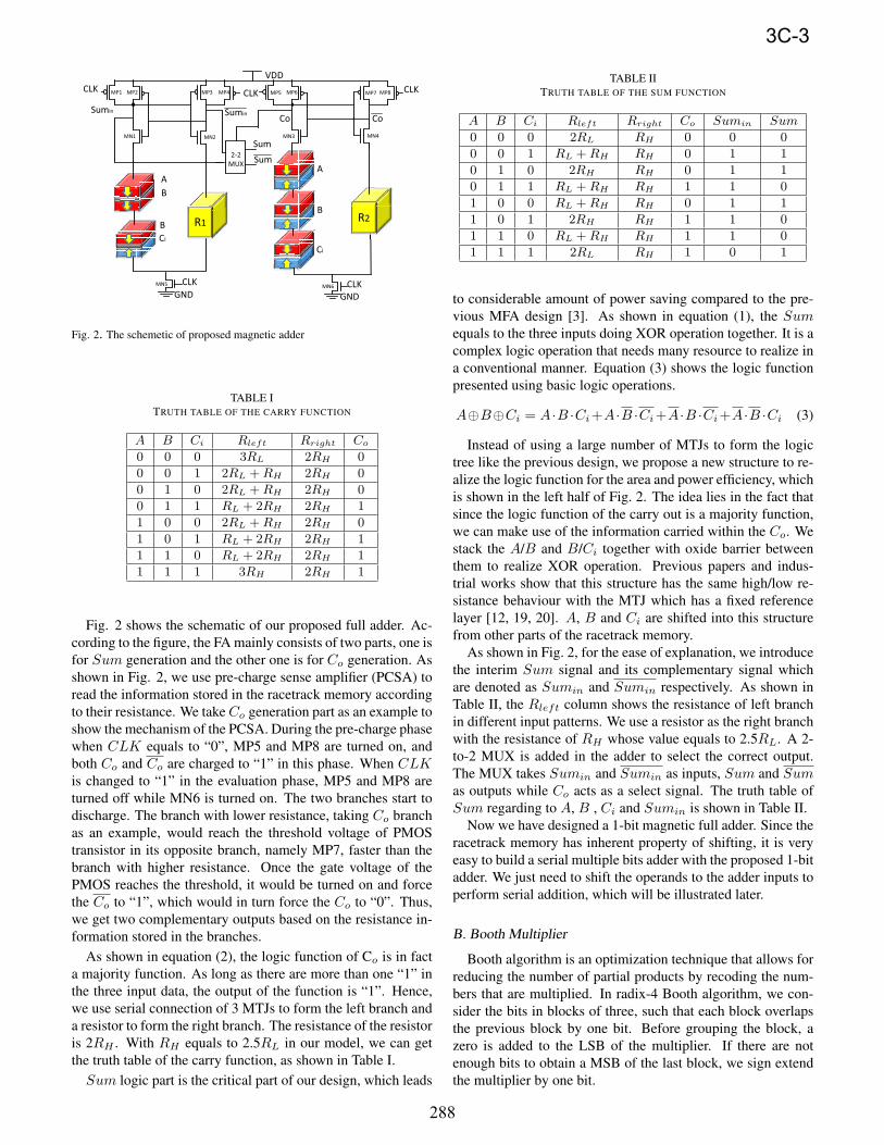
Fig. 2. The schemetic of proposed magnetic adder
TABLE I
TRUTH TABLE OF THE CARRY FUNCTION
A B Ci Rleft Rright Co
0 0 0 3RL 2RH 0
0 0 1 2RL +RH 2RH 0
0 1 0 2RL +RH 2RH 0
0 1 1 RL + 2RH 2RH 1
1 0 0 2RL +RH 2RH 0
1 0 1 RL + 2RH 2RH 1
1 1 0 RL + 2RH 2RH 1
1 1 1 3RH 2RH 1
Fig. 2 shows the schematic of our proposed full adder. Ac-
cording to the figure, the FA mainly consists of two parts, one is
for Sum generation and the other one is for Co generation. As
shown in Fig. 2, we use pre-charge sense amplifier (PCSA) to
read the information stored in the racetrack memory according
to their resistance. We take Co generation part as an example to
show the mechanism of the PCSA. During the pre-charge phase
when CLK equals to “0”, MP5 and MP8 are turned on, and
both Co and Co are charged to “1” in this phase. When CLKis changed to “1” in the evaluation phase, MP5 and MP8 are
turned off while MN6 is turned on. The two branches start to
discharge. The branch with lower resistance, taking Co branch
as an example, would reach the threshold voltage of PMOS
transistor in its opposite branch, namely MP7, faster than the
branch with higher resistance. Once the gate voltage of the
PMOS reaches the threshold, it would be turned on and force
the Co to “1”, which would in turn force the Co to “0”. Thus,
we get two complementary outputs based on the resistance in-
formation stored in the branches.
As shown in equation (2), the logic function of Co is in fact
a majority function. As long as there are more than one “1” in
the three input data, the output of the function is “1”. Hence,
we use serial connection of 3 MTJs to form the left branch and
a resistor to form the right branch. The resistance of the resistor
is 2RH . With RH equals to 2.5RL in our model, we can get
the truth table of the carry function, as shown in Table I.
Sum logic part is the critical part of our design, which leads
TABLE II
TRUTH TABLE OF THE SUM FUNCTION
A B Ci Rleft Rright Co Sumin Sum
0 0 0 2RL RH 0 0 0
0 0 1 RL +RH RH 0 1 1
0 1 0 2RH RH 0 1 1
0 1 1 RL +RH RH 1 1 0
1 0 0 RL +RH RH 0 1 1
1 0 1 2RH RH 1 1 0
1 1 0 RL +RH RH 1 1 0
1 1 1 2RL RH 1 0 1
to considerable amount of power saving compared to the pre-
vious MFA design [3]. As shown in equation (1), the Sumequals to the three inputs doing XOR operation together. It is a
complex logic operation that needs many resource to realize in
a conventional manner. Equation (3) shows the logic function
presented using basic logic operations.
A⊕B⊕Ci = A ·B ·Ci+A ·B ·Ci+A ·B ·Ci+A ·B ·Ci (3)
Instead of using a large number of MTJs to form the logic
tree like the previous design, we propose a new structure to re-
alize the logic function for the area and power efficiency, which
is shown in the left half of Fig. 2. The idea lies in the fact that
since the logic function of the carry out is a majority function,
we can make use of the information carried within the Co. We
stack the A/B and B/Ci together with oxide barrier between
them to realize XOR operation. Previous papers and indus-
trial works show that this structure has the same high/low re-
sistance behaviour with the MTJ which has a fixed reference
layer [12, 19, 20]. A, B and Ci are shifted into this structure
from other parts of the racetrack memory.
As shown in Fig. 2, for the ease of explanation, we introduce
the interim Sum signal and its complementary signal which
are denoted as Sumin and Sumin respectively. As shown in
Table II, the Rleft column shows the resistance of left branch
in different input patterns. We use a resistor as the right branch
with the resistance of RH whose value equals to 2.5RL. A 2-
to-2 MUX is added in the adder to select the correct output.
The MUX takes Sumin and Sumin as inputs, Sum and Sumas outputs while Co acts as a select signal. The truth table of
Sum regarding to A, B , Ci and Sumin is shown in Table II.
Now we have designed a 1-bit magnetic full adder. Since the
racetrack memory has inherent property of shifting, it is very
easy to build a serial multiple bits adder with the proposed 1-bit
adder. We just need to shift the operands to the adder inputs to
perform serial addition, which will be illustrated later.
B. Booth Multiplier
Booth algorithm is an optimization technique that allows for
reducing the number of partial products by recoding the num-
bers that are multiplied. In radix-4 Booth algorithm, we con-
sider the bits in blocks of three, such that each block overlaps
the previous block by one bit. Before grouping the block, a
zero is added to the LSB of the multiplier. If there are not
enough bits to obtain a MSB of the last block, we sign extend
the multiplier by one bit.
3C-3
288

1 01010110
-1-1-12
0011001111111111
00110011111111
001100111111
0001011000
0011110110101000
00101100Multiplicand (52)
Multiplier(107)
Booth encoding of multiplier
Partial products
Result(5564)
Fig. 3. The operation of the Booth multiplication
TABLE III
ENCODING AND DECODING REGARDING TO MULTIPLICAND
Y2i−1 Y2i Y2i+1 Partial Product
0 0 0 0* Multiplicand
0 0 1 1* Multiplicand
0 1 0 1* Multiplicand
0 1 1 2* Multiplicand
1 0 0 -2* Multiplicand
1 0 1 -1* Multiplicand
1 1 0 -1* Multiplicand
1 1 1 0* Multiplicand
For example, if we have a multiplier and a multiplicand
which are “01101011” and “00110100” respectively, then we
can get four blocks, which are “110”, “101”, “101” and “011”.
According to the bits in the four blocks, denoted as Y2i−1, Y2i
and Y2i+1, we can get four partial products by the correspond-
ing recoding rule shown in Table III. In our example case, the
four partial products are multiplication of multiplicand with “-
1”, “-1”, “-1” and “2” consecutively. Then the sum up of the
four partial products gives the multiplication result. The opera-
tion of the Booth multiplication is illustrated in Fig. 3. The pro-
cedure of the Booth multiplier can be classified into two steps:
partial products generation and partial products addition. First
we present our implementation of the partial products genera-
tion.
B.1 Partial Products Generation
For the performance concern, we implement partial products
generation in parallel. Since we choose radix-4 Booth algo-
rithm, we need to implement radix-4 based Booth encoder and
decoder. Table III shows the encoding and decoding regarding
to different block inputs.
As shown in the table, Y2i−1, Y2i and Y2i+1 are digits of the
input blocks of the multiplier. “0*” means the partial product
equals to zero multiplying the multiplicand. It is the same for
“1*”, “2*”, “-1*” and “-2*” respectively. First, we need to de-
code the block inputs to decide which partial products is needed
for the multiplication. Then control signals are computed in
the encoding step according to the following equations (4)-(8)
to control the generation of corresponding partial products.
zero = Y2i−1 · Y2i · Y2i+1 + Y2i−1 · Y2i · Y2i+1 (4)
one = Y2i−1 · Y2i · Y2i+1 + Y2i−1 · Y2i · Y2i+1 (5)
two = Y2i−1 · Y2i · Y2i+1 (6)
ne two = Y2i−1 · Y2i · Y2i+1 (7)
ne one = Y2i−1 · Y2i · Y2i+1 + Y2i−1 · Y2i · Y2i+1 (8)
These logic functions can be very easily implemented by
CMOS logic. Since we need to generate the partial products
in parallel, the data stored in the racetrack memory need to be
re-organized in a certain fashion to enable the parallel opera-
tion.
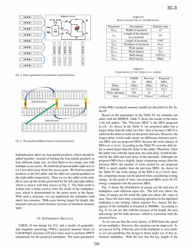
Fig. 4 shows the data organization of the multiplier and the
multiplicand. Although our design has great scalability and can
be applied to 64-bit multiplier, for simplicity, we use 8-bit data
as an example to illustrate the data organization and the data
flow in the multiplier. As shown in Fig. 4, the multiplicand Xis stored in the memory stripe in series, while the multiplier Yis stored in the separate memory stripes. This data organization
ensures that the bits of multiplier can be accessed concurrently,
so that the partial products can be generated in parallel. As
we can see from Fig. 4, if the multiplier has 8-bit, then there
are four partial products needed to be generated based on the
four 3-bit groups in the multiplier. According to different par-
tial products, there are different transformations needed to be
applied.
For radix-4 Booth algorithm, there are five kinds of trans-
formations which are “remain”, “negation”, “left-shifting”,
“plusing-one” and “setting-to-zero”. Among the five transfor-
mations, “remain” would not cause any change, and can be ig-
nored. “Negation” can be realized by applying a 2-to-2 MUX
controlled by control signals in front of writing circuits, which
is shown in Fig. 4. The selecting signal of the MUX can be
the result of OR function of ne one and ne two, which means
either signal is valid, negation would be applied to the multipli-
cand to generate the required partial products. “Left-shifting”
and “setting-to-zero” can be realized by controlling the shift-
ing circuit, which is shared with the racetrack memory itself.
Since the initial state of the racetrack memory is zero, “setting-
to-zero” means doing nothing. “Plusing-one” can be realized
by setting the initial Ci to “1” when conducting the addition
operation.
B.2 Addition of Partial Productions
After obtaining all the required partial products, we need to
sum them together. In order to exploit the inherent advantages
of racetrack memory, we pipeline the addition operation. Since
the racetrack memory itself can be used as the stage register,
the pipelined addition can be very deep, which is very efficient
for data intensive applications.
Fig. 5 shows the pipelined addition based on racetrack mem-
ory. For simplicity, we take 8-bit multiplication as an example,
which means the final result has the length of 16 bits. For the
ease of illustration, we use a single stripe in the figure to rep-
resent the stripe set of the corresponding operand. For 8-bit
3C-3
289
... Y14 Y6...
... Y13 Y5...
... Y12 Y4...
... Y11 Y3...
... Y10 Y2...
... Y9 Y1...
... Y8 Y0...
0 0 00
... Y15 Y7...
...X
1X
0...
...P
12P
11...
...P
22P
21...
...P
32P
31...
...P
42P
41...
W
W W
W
2-2MUX
input
input
W
W
ne_one ne_two
Negation circuit
Fig. 4. Data organization for generation of partial products
... ... ...W/R ... ... ...
W
/R ......... ... ... ...
... ... ......W
/R ... ... ... ... ... ......... ... ... ...
adde
r
... ... ...W/R ... ... ...
W
/R ......... ... ... ...
... ... ... ...
... ... ... ...
... ... ...W
/R
... ... ...W
/R
adde
rStripes of the operand
Stripes of the operandadde
r
Stripes of the result
Fig. 5. The pipelined addition based on racetrack memory
multiplication, there are four partial products, which should be
added together. Instead of feeding the four partial products to
four different stripe sets, we feed them to two stripes sets with
multiple access ports. We build the proposed adder right next to
(or a few units away from) the access ports. We feed two partial
products to the left adder and the other two partial products to
the right adder respectively. Then we use the adder in the mid-
dle to sum up the results generated by the left and right adders,
which is shown with blue arrows in Fig. 5. The final result is
written into a stripe used to store the result of the multiplica-
tion, which is demonstrated by the green arrow in the figure.
With such a structure, we can implement the multiplier with
much less resource. With cases having longer bit length, this
structure can save more resource in terms of racetrack memory
units.
IV. EXPERIMENT RESULTS
CMOS 45 nm design kit [21] and a model of perpendic-
ular magnetic anisotropy (PMA) racetrack memory based on
CoFeB/MgO structure [22] have been used to perform SPICE
simulations for the proposed multiplier. The main parameters
TABLE IV
MAIN PARAMETERS IN THE RM MODEL
Parameter Description Default value
WRT Width of racetrack 1F
LDLength of the domain
in a racetrack2F
LRT Length of racetrack 128F
TRT Thickness of racetrack 6nm
WEN Write energy 1pJ
WDE Write latency 5ns
SEN Shift energy 0.051pJ
SDE Shift latency 500ps
TABLE V
COMPARISON OF THE THREE FULL ADDERS
CMOS
FA
Previous
MFA
Proposed
MFA
Delay 100ps 180ps 240 ps
Energy 15fJ 7.6fJ 19fJ
Write operation NA 16 7
Area 11.04um2 3.36um2 1.142um2
of this PMA racetrack memory model are described in the Ta-
ble IV.
Based on the parameters in the Table IV, we simulate our
adder with the HSPICE. Table V shows the results of the three
1-bit full adders. The “Previous MFA” is the MFA proposed
in [3]. As shown in the Table V, our proposed adder has a
longer delay than the other two FAs. This is because a MUX is
added in the adder to trade for the power and area. However, the
longer delay would make nearly no difference between previ-
ous MFA and our proposed MFA, because the write latency of
RM is at ns level. According to the Table IV, even the shift de-
lay is much larger than the delay of the adder. Therefore, when
the adder runs with the input data, the total delay would be lim-
ited by the shift and write delay of the operands. Although our
proposed MFA has a slightly larger computing energy than the
previous MFA, the number of write needed by our proposed
MFA is much smaller than the previous MFA. As shown in
the Table IV, the write energy of the RM is at pJ level, thus,
the computing energy can be ignored when considering writing
energy. In this point of view, our proposed MFA saves 56.3%
energy compared with the previous MFA.
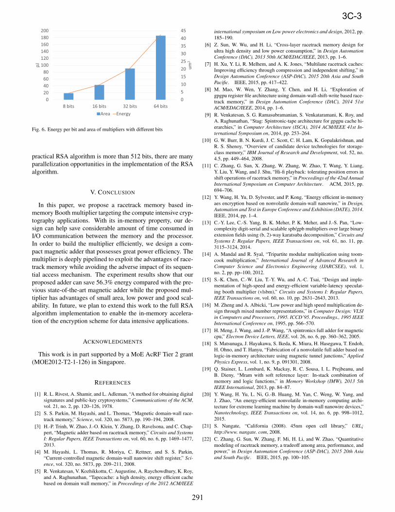
Fig. 6 shows the distribution of energy per bit and area of
multipliers with different input bits. The left axis shows the
value of energy per bit while the right axis shows the value of
area. Since the most time consuming operation in the pipelined
multiplier is the writing, which requires 5ns, hence, the fre-
quency of the multiplier is bounded at 200MHz. According to
Fig. 6, we can see that with the increase of bit length, the area
and energy per bit both increase, which is consistent with the
practical facts.
As we can see that the write latency of RM limits the speed
of our multiplier. However, this situation can be improved. As
we can see in Fig. 6 that the area of the multiplier is very small,
so we can parallelize the design to better make use of this in-
memory multiplier. With the fact that the key length of the
3C-3
290
051015202530354045
020406080
100120140160180200
8 bits 16 bits 32 bits 64 bits
um2
pJ
Area Energy
Fig. 6. Energy per bit and area of multipliers with different bits
practical RSA algorithm is more than 512 bits, there are many
parallelization opportunities in the implementation of the RSA
algorithm.
V. CONCLUSION
In this paper, we propose a racetrack memory based in-
memory Booth multiplier targeting the compute intensive cryp-
tography applications. With its in-memory property, our de-
sign can help save considerable amount of time consumed in
I/O communication between the memory and the processor.
In order to build the multiplier efficiently, we design a com-
pact magnetic adder that possesses great power efficiency. The
multiplier is deeply pipelined to exploit the advantages of race-
track memory while avoiding the adverse impact of its sequen-
tial access mechanism. The experiment results show that our
proposed adder can save 56.3% energy compared with the pre-
vious state-of-the-art magnetic adder while the proposed mul-
tiplier has advantages of small area, low power and good scal-
ability. In future, we plan to extend this work to the full RSA
algorithm implementation to enable the in-memory accelera-
tion of the encryption scheme for data intensive applications.
ACKNOWLEDGMENTS
This work is in part supported by a MoE AcRF Tier 2 grant
(MOE2012-T2-1-126) in Singapore.
REFERENCES
[1] R. L. Rivest, A. Shamir, and L. Adleman, “A method for obtaining digital
signatures and public-key cryptosystems,” Communications of the ACM,
vol. 21, no. 2, pp. 120–126, 1978.
[2] S. S. Parkin, M. Hayashi, and L. Thomas, “Magnetic domain-wall race-
track memory,” Science, vol. 320, no. 5873, pp. 190–194, 2008.
[3] H.-P. Trinh, W. Zhao, J.-O. Klein, Y. Zhang, D. Ravelsona, and C. Chap-
pert, “Magnetic adder based on racetrack memory,” Circuits and SystemsI: Regular Papers, IEEE Transactions on, vol. 60, no. 6, pp. 1469–1477,
2013.
[4] M. Hayashi, L. Thomas, R. Moriya, C. Rettner, and S. S. Parkin,
“Current-controlled magnetic domain-wall nanowire shift register,” Sci-ence, vol. 320, no. 5873, pp. 209–211, 2008.
[5] R. Venkatesan, V. Kozhikkottu, C. Augustine, A. Raychowdhury, K. Roy,
and A. Raghunathan, “Tapecache: a high density, energy efficient cache
based on domain wall memory,” in Proceedings of the 2012 ACM/IEEE
international symposium on Low power electronics and design, 2012, pp.
185–190.
[6] Z. Sun, W. Wu, and H. Li, “Cross-layer racetrack memory design for
ultra high density and low power consumption,” in Design AutomationConference (DAC), 2013 50th ACM/EDAC/IEEE, 2013, pp. 1–6.
[7] H. Xu, Y. Li, R. Melhem, and A. K. Jones, “Multilane racetrack caches:
Improving efficiency through compression and independent shifting,” in
Design Automation Conference (ASP-DAC), 2015 20th Asia and SouthPacific. IEEE, 2015, pp. 417–422.
[8] M. Mao, W. Wen, Y. Zhang, Y. Chen, and H. Li, “Exploration of
gpgpu register file architecture using domain-wall-shift-write based race-
track memory,” in Design Automation Conference (DAC), 2014 51stACM/EDAC/IEEE, 2014, pp. 1–6.
[9] R. Venkatesan, S. G. Ramasubramanian, S. Venkataramani, K. Roy, and
A. Raghunathan, “Stag: Spintronic-tape architecture for gpgpu cache hi-
erarchies,” in Computer Architecture (ISCA), 2014 ACM/IEEE 41st In-ternational Symposium on, 2014, pp. 253–264.
[10] G. W. Burr, B. N. Kurdi, J. C. Scott, C. H. Lam, K. Gopalakrishnan, and
R. S. Shenoy, “Overview of candidate device technologies for storage-
class memory,” IBM Journal of Research and Development, vol. 52, no.
4.5, pp. 449–464, 2008.
[11] C. Zhang, G. Sun, X. Zhang, W. Zhang, W. Zhao, T. Wang, Y. Liang,
Y. Liu, Y. Wang, and J. Shu, “Hi-fi playback: tolerating position errors in
shift operations of racetrack memory,” in Proceedings of the 42nd AnnualInternational Symposium on Computer Architecture. ACM, 2015, pp.
694–706.
[12] Y. Wang, H. Yu, D. Sylvester, and P. Kong, “Energy efficient in-memory
aes encryption based on nonvolatile domain-wall nanowire,” in Design,Automation and Test in Europe Conference and Exhibition (DATE), 2014.
IEEE, 2014, pp. 1–4.
[13] C.-Y. Lee, C.-S. Yang, B. K. Meher, P. K. Meher, and J.-S. Pan, “Low-
complexity digit-serial and scalable spb/gpb multipliers over large binary
extension fields using (b, 2)-way karatsuba decomposition,” Circuits andSystems I: Regular Papers, IEEE Transactions on, vol. 61, no. 11, pp.
3115–3124, 2014.
[14] A. Mandal and R. Syal, “Tripartite modular multiplication using toom-
cook multiplication,” International Journal of Advanced Research inComputer Science and Electronics Engineering (IJARCSEE), vol. 1,
no. 2, pp. pp–100, 2012.
[15] S.-K. Chen, C.-W. Liu, T.-Y. Wu, and A.-C. Tsai, “Design and imple-
mentation of high-speed and energy-efficient variable-latency speculat-
ing booth multiplier (vlsbm),” Circuits and Systems I: Regular Papers,IEEE Transactions on, vol. 60, no. 10, pp. 2631–2643, 2013.
[16] M. Zheng and A. Albicki, “Low power and high speed multiplication de-
sign through mixed number representations,” in Computer Design: VLSIin Computers and Processors, 1995. ICCD’95. Proceedings., 1995 IEEEInternational Conference on, 1995, pp. 566–570.
[17] H. Meng, J. Wang, and J.-P. Wang, “A spintronics full adder for magnetic
cpu,” Electron Device Letters, IEEE, vol. 26, no. 6, pp. 360–362, 2005.
[18] S. Matsunaga, J. Hayakawa, S. Ikeda, K. Miura, H. Hasegawa, T. Endoh,
H. Ohno, and T. Hanyu, “Fabrication of a nonvolatile full adder based on
logic-in-memory architecture using magnetic tunnel junctions,” AppliedPhysics Express, vol. 1, no. 9, p. 091301, 2008.
[19] Q. Stainer, L. Lombard, K. Mackay, R. C. Sousa, I. L. Prejbeanu, and
B. Dieny, “Mram with soft reference layer: In-stack combination of
memory and logic functions,” in Memory Workshop (IMW), 2013 5thIEEE International, 2013, pp. 84–87.
[20] Y. Wang, H. Yu, L. Ni, G.-B. Huang, M. Yan, C. Weng, W. Yang, and
J. Zhao, “An energy-efficient nonvolatile in-memory computing archi-
tecture for extreme learning machine by domain-wall nanowire devices,”
Nanotechnology, IEEE Transactions on, vol. 14, no. 6, pp. 998–1012,
2015.
[21] S. Nangate, “California (2008). 45nm open cell library,” URL¡http://www. nangate. com, 2008.
[22] C. Zhang, G. Sun, W. Zhang, F. Mi, H. Li, and W. Zhao, “Quantitative
modeling of racetrack memory, a tradeoff among area, performance, and
power,” in Design Automation Conference (ASP-DAC), 2015 20th Asiaand South Pacific. IEEE, 2015, pp. 100–105.
3C-3
291
Related Documents