INTRODUCTION TO PSPICE A QUICK GUIDE TO USING PSPICE 9.2 by Larry J. Klingenberg School of Engineering and Computer Science San Francisco State University January 2002 Introduction to PSpice

Welcome message from author
This document is posted to help you gain knowledge. Please leave a comment to let me know what you think about it! Share it to your friends and learn new things together.
Transcript
INTRODUCTION TO PSPICE
A QUICK GUIDE TO USING PSPICE 9.2
by
Larry J. Klingenberg
School of Engineering and Computer Science San Francisco State University
January 2002
Introduction to PSpice

TABLE OF CONTENTS INSTALL PSPICE FROM THE CD ROM.....................................................................................1
INITIALIZE GROUND REFERENCE FOR FIRST TIME USE.................................. 2
ADD PSPICE LIBRARIES ............................................................................................ 5
START A NEW PSPICE SCHEMATIC.........................................................................................8
PLACE PARTS IN SCHEMATIC ............................................................................... 10
SELECT PARTS FOR MOVING, DELETING, ROTATING.................................... 13
WIRE PARTS TOGETHER......................................................................................... 14
CHANGE A PART’S VALUE OR NAME ................................................................. 15
OPEN AN EXISTING SCHEMATIC...........................................................................................16
CHANGE A PART’S MODEL PARAMETERS..........................................................................18
CREATE A ± POWER SUPPLY WITH NET ALIAS ................................................................20
POWER SUPPLY CONNECTIONS ........................................................................... 20
CIRCUIT CONNECTIONS ......................................................................................... 21
COPY A PSPICE SCHEMATIC INTO A WORD DOCUMENT ...............................................22
COPY A PSPICE WAVEFORM INTO A WORD DOCUMENT ...............................................24
DC NODAL ANALYSIS ..............................................................................................................25
TRANSIENT ANALYSIS.............................................................................................................27
USE ALIASES TO IDENTIFY CIRCUIT AREAS..................................................... 27
ESTABLISH PARAMETERS (PROFILE) FOR TRANSIENT ANALYSIS............. 29
CREATE TRANSIENT ANALYSIS PLOT................................................................ 30
CREATE A STEP VOLTAGE SOURCE ................................................................................ 32
Introduction to PSpice

CREATE A REPEATING VOLTAGE SOURCE ................................................................... 33
CREATE AN IMPULSE .............................................................................................. 35
CREATE A SQUARE WAVE ..................................................................................... 35
CREATE A TRIANGULAR WAVE ........................................................................... 35
DC SWEEP....................................................................................................................................36
ESTABLISH PARAMETERS (PROFILE) FOR DC SWEEP .................................... 37
CREATE DC SWEEP PLOT ....................................................................................... 38
CHANGE AXIS FROM LINEAR TO LOG PLOT..................................................... 40
DC SWEEP – FAMILY OF CURVES..........................................................................................41
PRIMARY SWEEP ...................................................................................................... 42
SECONDARY SWEEP................................................................................................ 43
PLOT FAMILY OF CURVES ..................................................................................... 44
AC SWEEP....................................................................................................................................46
AC SWEEP – BODE PLOTS....................................................................................... 48
PARAMETRIC PLOT...................................................................................................................51
PLACE TEXT, LINES, ARROWS, ETC. IN THE PLOTS .........................................................55
USING CURSORS IN THE PLOT ...............................................................................................56
MARK CURSOR COORDINATES INTO THE PLOT.............................................. 57
Introduction to PSpice

INSTALL PSPICE FROM THE CD ROM To install PSpice from the CD ROM, insert the CD into the computer. The installation program
will auto-start.
Check Capture, PSpice, and Layout in the installation process.
Select Next > on this screen and the following screens until installation is complete.
Introduction to PSpice 1

INITIALIZE GROUND REFERENCE FOR FIRST TIME USE
o When PSpice is initially installed (for the first time from the CDROM), the “Ground”
reference must be configured so circuits can be simulated. The default “Ground” with
the installation will not work for simulations. First start a new PSpice schematic (page8).
o To install the proper ground, Select Place Æ Ground.
o Highlight CAPSYM; Select Remove Library to remove these symbols.
o Select Add Library to access Library folder.
Introduction to PSpice 2

o When the Library folder appears, double click to open the PSpice folder.
Note: Only the libraries located in the PSpice folder will work with simulations.
The other libraries in the Library folder can be used for the convenience of
drawing schematics when simulation is not required.
o
PSpice folder
Introduction to PSpice 3

o In the PSpice folder, select source.olb; select Open. This adds the library that contains a
Ground reference that is compatible with simulations.
o In the “Place Ground” screen that follows there are three choices: $D_HI, $D_LO, and 0.
Always select the “0” for the ground reference on schematics that you create.
o Select Cancel to quit. The initialization process for the ground reference is complete.
o The ground configuration process will not have to be performed again unless PSpice is
reinstalled.
Introduction to PSpice 4

ADD PSPICE LIBRARIES
o To install the most commonly used libraries, select Place Æ Part.
o o Select Add Library to bring up the PSpice library screen.
o
Introduction to PSpice 5

o In the PSpice library, select analog.olb, eval.olb, and source.olb. Select Open to install
these libraries.
All three libraries can be installed at once by using the CTL key on the keyboard
when selecting the library with the mouse. The alternative is to install each one
separately by selecting Add Library as before and selecting the library to install.
Introduction to PSpice 6

o The libraries are now installed and the parts are available for placement into schematics.
o
o Press Cancel when done.
Installed Libraries
Available Parts in the selected Libraries
Introduction to PSpice 7

START A NEW PSPICE SCHEMATIC
o The file that executes PSpice is called “capture.exe”. Create a shortcut to the
“capture.exe” file to run PSpice from the Windows Desktop, if not already done.
o After starting PSpice, select from the menu, File Æ New Æ Project.
o Fill in Name ______ (name the schematic with any name).
o Select ∑ Analog or Mixed A/D.
o Select Location _____ (select any location for your schematic files to be saved).
Note: The use of the floppy drive (usually A: ) location is much slower in terms
of saving the schematic than a hard drive location, but may be more useful.
o
o Select OK
Introduction to PSpice 8

o In the next screen, select ∑Create a blank project
o Select OK.
o
o A schematic page will appear. Parts are ready to be placed in the schematic.
o
Schematic page
Introduction to PSpice 9

PLACE PARTS IN SCHEMATIC
o With the schematic page in view, from the menu, select Place Æ Part.
o Select ANALOG library to pick components from the Part List such as resistors,
capacitors, or inductors.
o Select OK to place the part in your schematic.
o
Introduction to PSpice 10

o The part is now placed into the schematic.
Part List
Library
Part is placed to schematicin
o Continue placing parts from the available three libraries: ANALOG, EVAL, and
SOURCE.
Select SOURCE library to pick power sources, such as VDC, IDC, VAC, etc.
Select a power source from the Part List. Select OK to enter each part.
Select EVAL library to pick components from the Part List such as diodes,
transistors, JFETs, MOSFETs, Op Amps, and switches.
o After placing a part in the schematic, use the ESC key to return the cursor to normal
mode, otherwise each click of the mouse will continue placing copies of the part.
Introduction to PSpice 11

o To place a ground reference in a schematic, select Place Æ Ground.
o
o Select 0/SOURCE; select OK.
o
o The part will now be attached to the cursor and with each click of the cursor a copy will
be pasted into the schematic.
o Use the ESC key when done to return the cursor to normal mode, otherwise each
click of the mouse will continue placing copies of the part.
Introduction to PSpice 12

SELECT PARTS FOR MOVING, DELETING, ROTATING o To select a part in the schematic for deleting, rotating, etc., click the part once. A red box
appears around the part.
An alternative to selecting a part is to press and hold the left mouse button down
and move the mouse down and to the right. A selection box appears. All parts
inside this box will be selected when the mouse is released.
•
Selection box
o To move a part, select the part, press and hold the left mouse button down on top of the
part and drag to new position.
o To delete a part, select it, then delete using the DELETE key.
o To rotate or mirror a part select it, then from the menu Edit Æ Rotate, or Edit Æ Mirror.
•
Introduction to PSpice 13

WIRE PARTS TOGETHER
o From the menu, select Place Æ Wire.
o Click and release left mouse button on first terminal to connect.
o Drag mouse to second terminal to connect. A red dot appears momentarily when a
connection is made. Click the left mouse button to connect.
V15Vdc
R1
1k
0
R2
1k
Wire
Momentary red dot showing that a connection has
been made
o Continue in this manner until all parts are wired. Move and rotate parts as necessary
before wiring. Parts can be moved after wiring. Use ESC key to terminate the wiring
mode and return the cursor to the normal mode.
V15Vdc
R1
1k
0
R2
1k
Introduction to PSpice 14
CHANGE A PART’S VALUE OR NAME
o Double click the value or name to display the properties.
o Change the value or name. Select OK.
V1
5Vdc
R1
1k
0
LOAD
25k
Part value
Part name
o Note: For resistors in the megohm region, use the suffix Meg, such as 2.2Meg. The
upper and lower case “M” are interpreted by PSpice as “milli”.
Introduction to PSpice 15

OPEN AN EXISTING SCHEMATIC
To open an existing schematic, go to File → Open → Project ... and choose the
schematic (project) you want to open from the Windows menu of files and
folders.
o
Introduction to PSpice 16

Note: When opening an existing project that contains the schematic, sometimes
the “Heirarchy” box will appear instead of the schematic. Click all the “+” signs
until you reach “Page 1”. Double-click that. The schematic will then open.
•
Double-click this to open schematic
Introduction to PSpice 17

CHANGE A PART’S MODEL PARAMETERS
o Sometimes it is necessary to change a part’s default parameters (such as for a diode or
transistor).
Select the part in the schematic. A red dotted box appears around the part.
From the menu, select Edit Æ PSpice Model.
Diode is “selected” when box is visible
around it
o A screen appears showing the part’s parameters. Change the desired parameters.
o Select File Æ Save in the PSpice Model screen and close that screen. The parameters
are now changed for that part and each instance of its use in the current schematic; i.e., all
diodes of that type in the schematic are also changed. New (project) schematics are not
affected.
Introduction to PSpice 18

Model parameters
Introduction to PSpice 19

CREATE A ± POWER SUPPLY WITH NET ALIAS
o To save a lot of wiring in the schematic especially with power supply connections, a Net
Alias can be used to identify a circuit connection. A Net Alias is simply a tag that is
attached to the wire to associate the connection with a name. Other connections with the
same Net Alias (tag name) are considered connected.
POWER SUPPLY CONNECTIONS
o From the menu, use Place Æ Net Alias...
o A box appears requesting an Alias name. Use Vcc for the Positive power supply
connection. For the Negative power supply connection, use Vee. Any name will actually
work.
o Select OK.
Introduction to PSpice 20
CIRCUIT CONNECTIONS
o Shown below are examples of how Net Aliases can be used to “connect” wires together
instead of directly connecting them. (Note: pin 4 labeled “V+” is connected to “Vcc”
and pin 11 labeled “V-“ is connected to “Vee”. Always connect the “V+” of the op amp
to the positive power supply and the “V-“ to the negative power supply.)
o Net Aliases are not restricted for use on power supply connections. Notice in the
schematic how point A also completes a circuit.
R21k1.091V
0V
R110k
R4
1k
R7
3k
0V-12.00V
RL330
4.000V
6.000V
R3
1k
1.090V
0
R6
1k 6.000V
U3A
LM324
1
3
2
114
OUT
+
-
V-V+
V412Vdc
12.00V
0V
0
R5
1k
V312Vdc
-4.000V
0
Vee
Vcc
Vcc
Vcc
Vee
AA
LOAD
Vcc
Vee
Net Alias
Net Alias
The voltages displayed are in response to a DC Nodal Analysis, showing that the circuits are
“connected” together.
Introduction to PSpice 21

COPY A PSPICE SCHEMATIC INTO A WORD DOCUMENT
o To select the schematic parts that you want to paste into the Word document, drag a box
around those parts. The parts within the box are selected.
Note: Use Edit Æ Select All from the menu if you want to include everything in
the schematic page including the title box in the lower right hand corner of the
schematic.
Box created by dragging mouse
Parts inside box are “selected”
o When the parts are selected, go to the menu and select Edit Æ Copy.
•
Introduction to PSpice 22

o The parts selected in the schematic are now in the Windows Clipboard.
o Go to the Word document and place the cursor where you want the schematic to be
placed. In the Microsoft Word menu, select Edit Æ Paste to paste the schematic into the
Word document.
o
Introduction to PSpice 23

COPY A PSPICE WAVEFORM INTO A WORD DOCUMENT
o The method used to copy schematics does not work for waveforms generated by PSpice.
If you use Edit Æ Copy from the waveform menu, it will copy only columns of numbers.
o Instead, use Window Æ Copy to Clipboard... ; use the defaults for Background and
Foreground. For best printout, use “change all colors to black” for Foreground.
o Go to the Word document and
place the cursor in the document
where you want to put the
waveform. In Word, select Edit
Æ Paste to paste the waveform
in the document.
Introduction to PSpice 24

DC NODAL ANALYSIS
o Assume a schematic has a VDC source, two Resistors, and a Ground wired together.
o First create simulation settings for DC Nodal Analysis. Select from the menu, PSpice Æ
New Simulation Profile (or Edit Simulation Profile if a profile was previously done.)
o Fill in any name for Name: ______; select Create.
o Select Analysis tab if it is not already selected; select Analysis type: (drop down menu)
Bias Point; select OK.
o
Analysis tab
o Select PSpice Æ Run to begin the DC Nodal Analysis.
o If there were no errors, close the blank simulation screen to get back to the schematic.
Introduction to PSpice 25

o To show Current, Voltage, and/or Power; select from the menu, PSpice Æ Bias Points
Æ Enable (Current, Voltage, and/or Power).
o
o Your schematic will then appear with markers showing the Voltage, Current, and/or
Power values depending on which Display was enabled.
o
V110Vdc
10.00V
R3
1k6.667V
R2
1k
0
3.333V
R1
1k
Voltage Marker
Introduction to PSpice 26

TRANSIENT ANALYSIS
o Transient analysis is used when plotting the magnitude of a waveform versus time. This
is what is viewed on an oscilloscope.
o Assume we have a schematic with a VDC source (change the value to a desired voltage),
a Resistor and Capacitor (change to desired values), and a Ground wired together in
series.
USE ALIASES TO IDENTIFY CIRCUIT AREAS
o In order to make the traces in analysis easier to identify, you should name the significant
points with a Net Alias. A Net Alias is simply a tag that is attached to the wire to
associate the connection with a name.
o Examples of Net Alias’ are Vin, Vsource, Vout, etc.
o Placing a Net Alias is recommended before plotting. The plot will then have names of
traces corresponding to the Alias you created.
To create a Net Alias, from the menu, use Place Æ Net Alias...
Introduction to PSpice 27

A box appears requesting an Alias name. Use a name such as Vout or Vsource,
Vs, V1, etc.; select OK.
The Alias name is now attached to the cursor in your schematic. Attach it to a
wire that you want to identify as your alias. The alias name will attach only to a
wire (top or right side of the wire only). Use ESC to finish placing the alias
part and return cursor to normal mode.
R1
1k
0
C1
1uF
V15Vdc
VoutVsource
Net Alias called “Vsource”
Net Alias called “Vout”
Introduction to PSpice 28

ESTABLISH PARAMETERS (PROFILE) FOR TRANSIENT ANALYSIS
o After placing aliases, the Transient Analysis profile must be created.
o From the menu, select PSpice Æ New Simulation Profile. If you’ve already done other
simulations, you can simply use PSpice Æ Edit Simulation Profile and change the
necessary parameters.
o Fill in any name for Name: ______; select Create.
This step is not necessary if you Edit Simulation Profile.
o Select Analysis tab if it is not already selected; select Analysis type: (drop down menu)
Time Domain (Transient) which is usually the default; select OK.
o Select Run Time ______ (enter a value for how much time is to be displayed in the time
domain).
o Enter a check in the box called: √Skip the initial transient bias point calculation for
initial conditions to be zero (this is a very important step).
o Select OK.
o
This must have a checkmark
Introduction to PSpice 29

CREATE TRANSIENT ANALYSIS PLOT
o Establish the dependent variable to be plotted. In this example the voltage on the
schematic with the alias called Vout is to be plotted.
o From the menu, go to PSpice → Markers → Voltage Level and attach a Voltage Level
probe corresponding to the desired output.
Voltage Level Probe
Introduction to PSpice 30

o From the menu, select PSpice Æ Run to begin the Transient Analysis.
o
o If there are no errors, the plot will appear. If the plot was used before, sometimes the plot
will remain minimized in the Windows taskbar. Click the minimized box called
“SCHEMATIC” to maximize the plot.
Time
0s 1ms 2ms 3ms 4ms 5ms 6ms 7ms 8ms 9ms 10msV(VOUT)
0V
1.0V
2.0V
3.0V
4.0V
5.0V
Introduction to PSpice 31

CREATE A STEP VOLTAGE SOURCE
o Using a switch gives the added flexibility for creating a step voltage anywhere in the
schematic. A ‘time delay before closing’ parameter is adjustable on the switch.
o Use the Place Æ Part Æ EVAL Æ Sw_tClose
Assuming you have a schematic with a power source (usually VDC), place the
Sw_tClose in series with the load. This is a normally open switch which will
close at time=0 (default). The ‘time delay before closing’ can be redefined by
clicking the TCLOSE and changing the value from 0 to another value; for
example, 0.1mS. In this example, the switch will close at time = 0.1 mS.
o
R1
1k
0
C1
1uF
V15Vdc
U1
TCLOSE = 0.1mS
1 2
V
Vout
Vsource
Voltage Level Probe
In the setup of transient analysis (see TRANSIENT ANALYSIS), the √Skip the
initial transient bias point calculation box must be checked for initial
conditions to be zero.
o As before, provide a Net Alias and a Voltage Level probe.
PSpice → Markers → Voltage Level and attach the Voltage Level probe
corresponding to the output desired, Vout
o From the menu, select PSpice Æ Run to begin the Transient Analysis.
o The plot will appear on the screen (or sometimes as a minimized icon called
“SCHEMATIC” in the Windows taskbar at the bottom).
Introduction to PSpice 32

CREATE A REPEATING VOLTAGE SOURCE
o To create a repeating impulse, square wave, or triangular wave, use the Place Æ Part Æ
SOURCE Æ VPULSE from the menu.
Note: For a current source, use IPULSE. The same technique applies.
Introduction to PSpice 33

o There are seven parameters to set up which will determine the waveform.
V1 is the lower voltage level.
V2 is the upper voltage level.
TD is the time delay before starting the waveform. Usually this is set to zero.
TR is the rise time. PSpice will not allow this to be zero!
• A reasonable value for a very fast risetime is 1mS for a pulse or square
wave.
• For a triangular wave, this will be whatever time for the triangle ramp to
ramp up.
TF is the fall time. PSpice will not allow this to be zero!
• A reasonable value for a very fast falltime is 1mS for a pulse or square
wave.
• For a triangular wave, this will be whatever time for the triangle ramp to
ramp down.
PW is the width of the pulse. PSpice will not allow this to be zero!
PER is the period of the waveform.
PER
PW
TF TR
V2
V1
WAVEFORM DEFINITIONS
Introduction to PSpice 34

CREATE AN IMPULSE
V1 will ordinarily be zero. V2 is the upper voltage level and should be a large value. 10 Volts is an
acceptable value. TD usually set to zero. TR and TF should be fast, on the order of 1mS or less. PW should be very short, 1mS or less. PER should be very long, typically 100mS to 1S depending on the circuit so that
the impulses appear very far apart. Example for an impulse
• V1=0; V2=10; TD=0; TR=0.1mS; TF=0.1mS; PW=0.1mS; PER=1S
CREATE A SQUARE WAVE
V1 is the lower voltage level. V2 is the upper voltage level. TD usually set to zero. TR and TF should be fast, on the order of 1mS. PW should be whatever is desired. PER should be 2 x (PW+TR+TF) for a symmetrical square wave.
Example for 1kHz, 0-5v, 50% duty cycle square wave
• V1=0; V2=5; TD=0; TR=1mS; TF=1mS; PW=498mS; PER=1000mS
Example for 100kHz, 0-5v, 50% duty cycle square wave • V1=0; V2=5; TD=0; TR=0.01mS; TF=0.01mS; PW=4.98mS; PER=10mS
CREATE A TRIANGULAR WAVE
V1 is the lower voltage level. V2 is the upper voltage level. TD usually set to zero. TR and TF should be a ramp with desired ramp time. PW should ideally be zero for a triangular wave, but PSpice will not work
correctly if it is zero. Therefore, make PW very short, on the order of 1mS or less. PER should be TR + PW + TF for a continuous symmetrical triangular waveform.
Example for 1kHz, 0-5v, symmetrical triangular wave
• V1=0; V2=5; TD=0; TR=500mS; TF=499mS; PW=1mS; PER=1000mS
Example for 100kHz, 0-5v, symmetrical triangular wave • V1=0; V2=5; TD=0; TR=5mS; TF=4.99mS; PW=0.01mS; PER=10mS
Introduction to PSpice 35

DC SWEEP
o The DC Sweep capability allows you to change currents or voltages to many values in
one test.
o For a voltage sweep, from the menu use the Place Æ Part Æ SOURCE Æ VDC as the
voltage source.
(For a current sweep, use the Place Æ Part Æ SOURCE Æ IDC).
o Assume we want the i-v curve for a diode. Our schematic consists of a VDC and a diode,
D1.
The VDC source defaults to a name V1. If you decide to change the name, it
must start with a “V” for DC Sweep to work; such as Vin, Vout, etc.
If you had used an IDC source it would default to a name I1. If you decided to
change the name, it must start with a “I” for DC Sweeps to work; such as Iin, Iout,
etc.
o When the schematic is complete, you are ready to set up the DC Sweep.
•
D1
D1N4002
0
V10Vdc
o Select PSpice Æ New Simulation Profile.
Note: Choose PSpice Æ Edit Simulation Profile if a profile was previously
done to your schematic. Otherwise additional files will be created for the new
simulation profile.
o Fill in any name for Name: ______; select Create.
Note: This applies only if a New Simulation Profile was created.
Introduction to PSpice 36

ESTABLISH PARAMETERS (PROFILE) FOR DC SWEEP
o Select Analysis tab if it is not already selected; select Analysis type: (drop down menu)
DC Sweep. In Options, make sure only the Primary Sweep is checked.
o In the same screen under Sweep Variable, select Voltage source, since that is our
independent variable.
Note: In the Name box, you must use the same name of the voltage source as on
the schematic. The voltage source must start with “V”; for example, Vin.
If we used current as the independent variable instead of voltage, the current
source in the schematic must start with “I”; for example, Iin.
o Under Sweep Type, select Linear or Logarithmic, depending on your needs. For semi-
log, use Linear.
Next fill in the Start value, End value, and Increment. For our diode example
where we are sweeping the voltage, we would set the Start value as 0V, the End
value as 1V, and the Increment as 0.001V.
o
o Select OK to return to the schematic.
Introduction to PSpice 37

CREATE DC SWEEP PLOT
o Establish the dependent variable (y-axis), which in this case is the diode current.
o From the menu, go to PSpice → Markers → Current Into Pin and attach the Current
probe corresponding to the output desired, the diode current. The Current Into Pin
probe cannot be placed on a wire. It must be placed on the pin of a part.
o
Current Into Pin Probe
Introduction to PSpice 38

o After the probe is placed, go to PSpice → Run to view results of the simulation.
o The plot will appear on the screen.
Note: If the plot had been used before, it sometimes remains as a minimized icon
called “SCHEMATIC” in the Windows taskbar at the bottom. Click the icon to
enlarge.
Probe Current (diode current)
Y-axis Diode current
X-axis Voltage sweep from 0 to 1 volt
Introduction to PSpice 39

CHANGE AXIS FROM LINEAR TO LOG PLOT
o To make the plot a semi-log plot, change the y-axis, which is the current through the
diode in our example, to a logarithmic scale.
In the plot menu, select Plot Æ Axis Settings... Æ Y Axis.
Under Scale, select Log.
In Axis Title box, put in a name for the Y-axis which will show up in the plot.
Select OK .
You now have a semi-log plot with the X-axis linear and the Y-axis logarithmic.
Note: In this menu that you can also modify the X Axis, X Grid, and Y Grid.
Introduction to PSpice 40

DC SWEEP – FAMILY OF CURVES
o This procedure would typically be used for the characteristic family of curves for a
bipolar junction transistor, in which the voltage is the “sweep” variable. The sweep
variable for a transistor is the collector-emitter voltage, shown on the x-axis typically
from 0 to 15 volts.
o The sweep variable could also be current or temperature when used in other family of
curves applications.
o Assume we want the family of curves for a bipolar transistor in which we want to know
the collector current for different values of base current throughout a range of collector-
emitter (C-E) voltage.
The sweep voltage, therefore, is the C-E voltage, which will be the x-axis.
Typically it will sweep from 0 volts to 15 volts.
Place a transistor in the schematic, Place Æ Part Æ EVAL Æ Q2N2222.
Place a DC Current Source, Place Æ Part Æ SOURCE Æ IDC, to the base of the
transistor. The value of the DC current is irrelevant and ignored in this procedure.
Therefore, the default value of 0Adc will work fine. If the name is changed, it
must start with an “I”.
Q1Q2N2222V1
0Vdc
0
I1
0Adc
I1 is the Secondary Sweep which corresponds to the
number of traces on the plot.
V1 is the Primary Sweep which corresponds to the
x-axis of the plot
Place a DC Voltage Source, Place Æ Part Æ SOURCE Æ VDC, between the
collector and emitter of the transistor. The value of the DC voltage attached to the
part is irrelevant and ignored in this procedure. Therefore, the default value of
0Vdc will work.
If the name is changed from the default V1, it must also start with a “V”.
Introduction to PSpice 41

PRIMARY SWEEP
o In the Simulation Settings, ensure that Options: Primary Sweep has a checkmark.
o Choose Voltage source since that is to be the x-axis.
o Name is filled in for the voltage source that corresponds to the name on the schematic.
In our example, V1 is the voltage source in the schematic and is filled in the Name box.
o Sweep type is chosen as either Linear or Logarithmic.
o Start value, End value, and Increment are filled out. For our example, use the voltage
start value as 0 volts, the end value as 15 volts, and the increment as 0.05 volts. The
range in this case should be somewhere between 0.0015 to 0.015.
Note: A small increment value makes a smoother plot but takes longer for the
program to draw. As a rule-of-thumb, the range should be:
100
1000ValueEndMaximumValueIncrement
ValueEndMinimumValueIncrement
=
=
•
Name of Voltage source Primary Sweep
is a Voltage source
Primary Sweep must have a checkmark
Introduction to PSpice 42

SECONDARY SWEEP
o Next we need to establish the different values of base current that we would like to use in
the plot. We do this by using a secondary variable, I1.
o In the same Simulation Settings screen, in the Options box, put a check mark by
Secondary Sweep.
o Use Current source as the Sweep variable with the Name that corresponds to the current
source in the schematic, I1.
o Make the Sweep type → Linear.
o Fill in Start value, End value, and Increment as desired.
These values will determine the number of traces displayed on the plot. In this
example, a plot with traces 10mA, 20mA, 30mA, 40mA, 50mA, 60mA, 70mA, 80mA,
90mA, and 100mA will be on the plot.
As an alternative to using the Start, End, and Increment values, you can use the
Value list, with the values separated by a comma or a space.
o Select OK.
Secondary Sweep must have a checkmark
Name of Current source The Secondary Sweep
is a Current source
Introduction to PSpice 43

PLOT FAMILY OF CURVES
o Now set up the dependent variable in the schematic that we want to plot (y-axis), which
in this case is the collector current.
o Go to PSpice → Markers → Current Into Pin and attach the Current probe
corresponding to the output desired, the collector current of Q1.
o
Current Into Pin Probe which corresponds to the y-axis on the plot
Introduction to PSpice 44

o Go to PSpice → Run to view DC Sweep Family of Curves.
V_V1
0V 2V 4V 6V 8V 10V 12V 14V 16VIC(Q1)
-5mA
0A
5mA
10mA
15mA
20mA
25mA
Base current 100uA
Base current 10uA
Secondary Sweep 10 Traces
(base current) Y-axis
Current Into Pin Probe (collector current)
X-axis Primary Sweep, 0 to 15 volts (collector – emitter voltage)
Introduction to PSpice 45
AC SWEEP
o AC Sweep is used for observing magnitude and phase of voltages and currents.
Use only the VAC or IAC for power sources.
o Create a schematic with VAC as the power source. (See example below). Use a Net
Alias to help identify relevant circuit areas when plotting is complete.
o Select PSpice Æ New Simulation Profile (or choose PSpice Æ Edit Simulation Profile
if a profile was previously done to your schematic).
If using New Simulation Profile, fill in any name for Name: ______.
Select Create.
o Select Analysis tab if it is not already selected; select Analysis type: (drop down menu),
AC Sweep/Noise; AC Sweep Type as Linear or Logarithmic; Start Frequency, End
Frequency, and Points/Decade. (Note: When used, always specify MegHz, not MHz).
o Click OK.
A reasonable value for Points/Decade is 100 to 1000. The more Points the longer
it takes to simulate and the smoother the curves.
Introduction to PSpice 46

o Go to PSpice → Markers → Voltage Level and attach the Voltage Level probe to the
output desired.
o o Go to PSpice → Run to view results of the simulation.
o
Voltage Level Probe
Voltage Level Probe results
Introduction to PSpice 47

AC SWEEP – BODE PLOTS
o Bode plots consist of two plots: magnitude of output to input (dB) versus frequency
(Hz), and phase (deg) versus frequency (Hz).
The schematic utilizes the VAC source and the Simulation Settings are set to AC
Sweep Type and Logarithmic in decades. Assume that the phase of the VAC
source is 0 degrees.
The phase vs frequency will be plotted automatically in a separate plot.
o The VAC source magnitude in the schematic must be equal to 1.
o Assume that you have drawn your schematic.
o Set up the Simulation Profile with AC Sweep, Logarithmic → Decade, Start
Frequency, End Frequency, Points/Decade.
Note: 100 to 1000 points per decade is a reasonable value.
o Select OK.
o
Introduction to PSpice 48

o Go to PSpice → Markers → Plot Window Templates ...
o Select Bode Plot dB – separate; select Place.
o A small probe appears at the end of you cursor. Attach this probe to the output desired
on your schematic. Next go to PSpice → Run to create the Bode plot.
o
Vac source voltage must be 1Vac
o
Bode Plot dB Probe
Introduction to PSpice 49

o The Bode Plot appears as two plots:
Magnitude (dB) vs frequency (Hz).
Phase (deg) vs frequency (Hz).
Frequency
10Hz 30Hz 100Hz 300Hz 1.0KHz 3.0KHz 10KHz 30KHz 100KHzP(V(VOUT))
0d
20d
40d
60dDB(V(VOUT))
-30
-20
-10
0
SEL>>
Introduction to PSpice 50

PARAMETRIC PLOT
o The Parametric Plot allows you to use different values of a part on the same plot. For
example, suppose you wanted to do a Transient Analysis of an RC circuit with three
different values of capacitance, 1mF, 10mF, and 100mF. Do the following:
Name the part value with a variable name (any name will do, but we shall use
“cval” as the variable name) enclosed in curly brackets. That is, instead of using
1mF for the value, use {cval}.
Note: Be sure to use a probe so that the plots will automatically be generated
when simulating. In this example, a voltage probe has been placed at Vout. As a
result, three plots will be generated showing the voltage vs. time for three values
of capacitance.
o Instead of a value such as 1uF,
we are giving it a variable name, in this case cval, and enclosing it
in curly brackets.
Introduction to PSpice 51

Declare the variable by going to PSpice Æ Place Optimizer Parameters and
place the Optimizer part in the schematic. (Declaring the variable means that we
are setting it up for PSpice to recognize it with more than one value.)
•
Optimizer part
• Open the Optimizer Parameter part just placed by double-clicking it.
• Fill in the Name with the variable name used, in this case, cval. Do not
use the curly brackets when filling in Name. Ignore the remaining boxes.
• Click Add to place the variable name in the window. Click OK. The
variable “cval” is now declared.
Double-click this to bring up window.
Clicking “Add” places cval in the window. Click “OK” when done.
Introduction to PSpice 52

After creating a Simulation Profile as Time Domain (Transient), select the Parametric Sweep to
bring up the parametric sweep options.
o Check the Parametric Sweep box
o Select the Global parameter
o Fill in the Parameter name, cval
o Select the Value list and fill in 1uF,10uF,100uF. The values must be in the order of
smallest value (1uF in this case) to the highest value (100uF). There must be no spaces
after the commas.
o Select OK when done.
Introduction to PSpice 53

Simulate the schematic as usual.
Before simulation is complete, a screen will appear. Click OK.
Click “OK” when this screen appears.
Three plots corresponding to three values of capacitance will be produced.
Time
0s 10ms 20ms 30ms 40ms 50ms 60ms 70ms 80ms 90ms 100msV(VOUT)
0V
1.0V
2.0V
3.0V
4.0V
5.0V
1uF
10uF
100uF
Introduction to PSpice 54

PLACE TEXT, LINES, ARROWS, ETC. IN THE PLOTS
o Clicking in the upper or lower plot, go to Plot → Label → Text ... (Line, Poly-line,
Arrow, Box, Circle, Ellipse).
Note: The SEL>> to the left of the plot informs you which plot is active for
inserting text (or other items).
o Select the item to place in the plot.
o Click in the plot to place the item.
o Move text (or other item) by clicking mouse cursor on it and dragging to new position.
Arrow placed into plot Text placed into plot
Introduction to PSpice 55
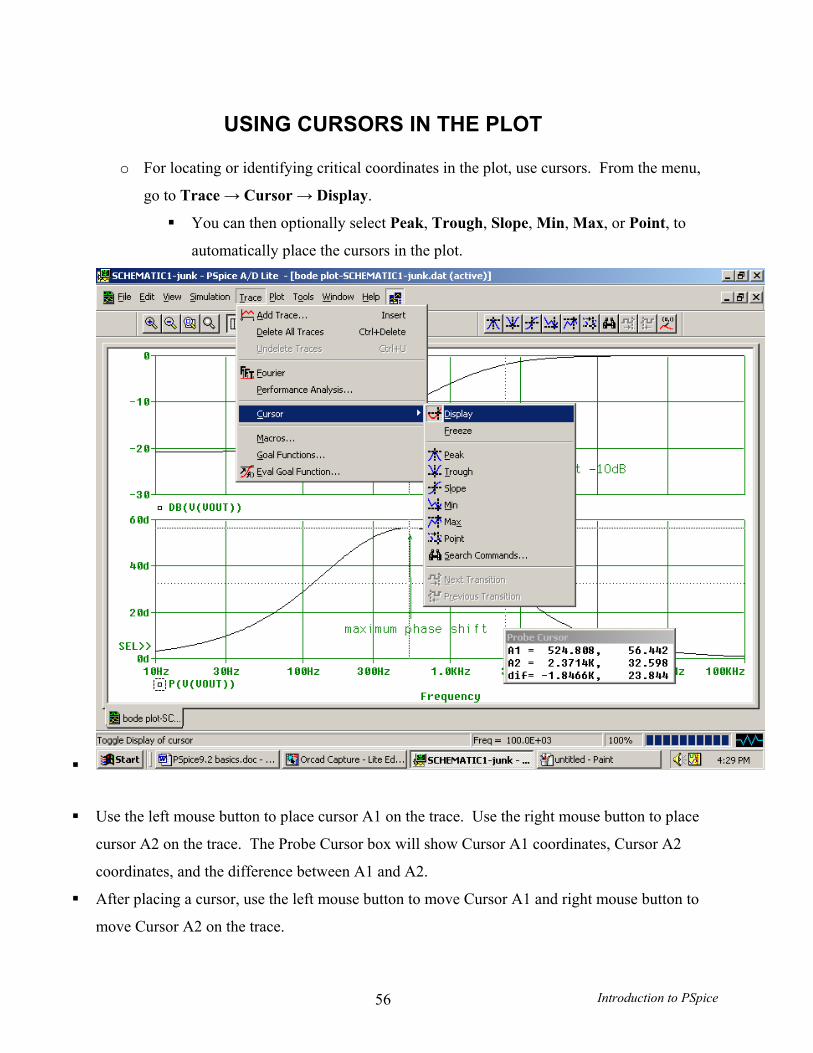
USING CURSORS IN THE PLOT
o For locating or identifying critical coordinates in the plot, use cursors. From the menu,
go to Trace → Cursor → Display.
You can then optionally select Peak, Trough, Slope, Min, Max, or Point, to
automatically place the cursors in the plot.
Use the left mouse button to place cursor A1 on the trace. Use the right mouse button to place
cursor A2 on the trace. The Probe Cursor box will show Cursor A1 coordinates, Cursor A2
coordinates, and the difference between A1 and A2.
After placing a cursor, use the left mouse button to move Cursor A1 and right mouse button to
move Cursor A2 on the trace.
Introduction to PSpice 56
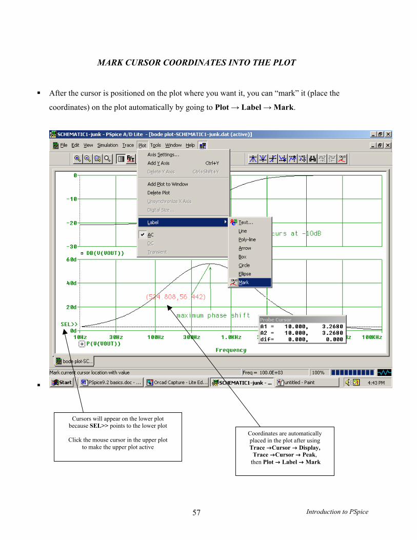
MARK CURSOR COORDINATES INTO THE PLOT After the cursor is positioned on the plot where you want it, you can “mark” it (place the
coordinates) on the plot automatically by going to Plot → Label → Mark.
Cursors will appear on the lower plot because SEL>> points to the lower plot
Click the mouse cursor in the upper plot
to make the upper plot active
Coordinates are automatically placed in the plot after using Trace ÆCursor Æ Display,
Trace ÆCursor Æ Peak, then Plot Æ Label Æ Mark
Introduction to PSpice 57

NOTES
Introduction to PSpice 58
Related Documents