1392 Journal of Engineering Sciences Assiut University Faculty of Engineering Vol. 42 No. 6 November 2014 PP. 1392 – 1413 * Corresponding author. E-mail address: [email protected] A PROPOSED DESIGN OF UWB MONOPOLE ANTENNA AND ITS LINEAR ARRAYS Hosny El Metaafy 1 , Mahmoud Mohana 2 , Ali Gomaa 3 , Mamdouh Shaker Yacoub 4 and Gamal Kassem *, 5 1, 5 Higher Technological Institute 10 th of Ramadan city (H.T.I) 2 National Research Institute of Astronomy and geophysics (NRIAG) 3 Faculty of Engineering, Shoubra, Benha University 4 High Obour Institute (Received 12 November 2014; Revised 12 December 2014; Accepted 15 December 2014) ABSTRACT A proposed design of ultra-wideband (UWB) monopole antenna has been presented to cover frequency range 2.49–14.42 GHz with small size. An equivalent circuit model with the parameter values of the optimized UWB antenna has been modeled. Moreover, a compatible lumped-elements utilized in equivalent circuit modeling for the proposed monopole antenna is established using the Advanced Design System (ADS). An UWB feeding network circuit has been designed in order to be used for exciting 2x1 and 4x1 linear antenna array. The measured and simulated results for the proposed feed network has a good return loss, isolation and power division ratio at all ports within the whole UWB frequency range. Two and four element UWB linear antenna arrays are presented. The average gain for the two-element antenna array is about 5.3 dBi and reaches to7.15 dBi for the four-element antenna array, over the whole UWB frequency range. A good agreement between the measured and the simulated results of all parameters for the antenna element and antenna arrays is appeared. Keywords: monopole antenna, Ultra-wide band, antenna array, power divider, stubs matching. 1. Introduction Recently, the unlicensed Ultra-wideband (UWB) technology for commercial communications released by the Federal Communication Commission (FCC) is used in several applications. The concept of UWB radio was first developed several decades ago exactly in the late1960’s. The U.S. Development of Defense first founded the term ‘Ultra wideband’ in 1989 [1]. In the beginning, UWB was mainly for military purposes such as radar applications which use wideband signals in frequency domain or very short duration pulses in the time domain to get fast, reliable and accurate information about moving targets such missiles. UWB technology has a great interest especially in 2002 since the US Federal Communication Commission (FCC) allowed the using of the unlicensed frequency

Welcome message from author
This document is posted to help you gain knowledge. Please leave a comment to let me know what you think about it! Share it to your friends and learn new things together.
Transcript

1392
Journal of Engineering Sciences
Assiut University
Faculty of Engineering
Vol. 42
No. 6
November 2014
PP. 1392 – 1413
* Corresponding author.
E-mail address: [email protected]
A PROPOSED DESIGN OF UWB MONOPOLE
ANTENNA AND ITS LINEAR ARRAYS
Hosny El Metaafy 1, Mahmoud Mohana
2,
Ali Gomaa 3, Mamdouh Shaker Yacoub
4 and Gamal Kassem
*, 5
1, 5 Higher Technological Institute 10
th of Ramadan city (H.T.I)
2 National Research Institute of Astronomy and geophysics (NRIAG)
3 Faculty of Engineering, Shoubra, Benha University
4 High Obour Institute
(Received 12 November 2014; Revised 12 December 2014; Accepted 15 December 2014)
ABSTRACT
A proposed design of ultra-wideband (UWB) monopole antenna has been presented to cover frequency
range 2.49–14.42 GHz with small size. An equivalent circuit model with the parameter values of the
optimized UWB antenna has been modeled. Moreover, a compatible lumped-elements utilized in
equivalent circuit modeling for the proposed monopole antenna is established using the Advanced
Design System (ADS). An UWB feeding network circuit has been designed in order to be used for
exciting 2x1 and 4x1 linear antenna array. The measured and simulated results for the proposed feed
network has a good return loss, isolation and power division ratio at all ports within the whole UWB
frequency range. Two and four element UWB linear antenna arrays are presented. The average gain for
the two-element antenna array is about 5.3 dBi and reaches to7.15 dBi for the four-element antenna array,
over the whole UWB frequency range. A good agreement between the measured and the simulated
results of all parameters for the antenna element and antenna arrays is appeared.
Keywords: monopole antenna, Ultra-wide band, antenna array, power divider, stubs matching.
1. Introduction
Recently, the unlicensed Ultra-wideband (UWB) technology for commercial
communications released by the Federal Communication Commission (FCC) is used in
several applications. The concept of UWB radio was first developed several decades ago
exactly in the late1960’s. The U.S. Development of Defense first founded the term ‘Ultra
wideband’ in 1989 [1]. In the beginning, UWB was mainly for military purposes such as
radar applications which use wideband signals in frequency domain or very short duration
pulses in the time domain to get fast, reliable and accurate information about moving
targets such missiles. UWB technology has a great interest especially in 2002 since the US
Federal Communication Commission (FCC) allowed the using of the unlicensed frequency

1393
Gamal kassem et al., A proposed design of UWB monopole antenna and its linear arrays
band starting from 3.1 to 10.6 GHz for commercial communication applications [2]. The
allocated FCC bandwidth is 7.5 GHz which represent 110% fractional bandwidth of the
center frequency. Ultra wide band technology plays a paramount role in the development
of modern wireless communication devices by transmitting videos, audios and other high
bandwidth data between multiples of devices in the vicinity of 10 m or 30 ft, which covers
the appliances used in home or office achieving high speed transfer, between 40 to 60
megabits per seconds and recently may reach up to 1 gigabits per second, low cost and low
power consumption (0.5mW). The major applications for the UWB are the commercial
communication systems, like vehicular radar systems, imaging systems such as ground-
penetrating radar, wall-imaging systems, medical systems, and surveillance systems. Also,
in Wireless Personal Area Networks (WPANs) environments, UWB technology is an
excellent solution for the ultra-high-speed data services up to 500 Mbps. These speeds can
be greatly increased by using antenna arrays instead of single antenna element and
different beam forming techniques. In order to design UWB antenna array, the power
divider circuits are required. The most popular power divider is the Wilkinson power
divider [3]. However, it operates only in a narrow bandwidth so; it is a serious problem for
the UWB application. In order to achieve the bandwidth of UWB (3.1-10.6GHz), a three-
section Wilkinson power divider has been reported, which increases the bandwidth [4].
Many efforts have been introduced to meet this challenge. One is to use a narrow rectangle
slot to couple the wave from the input to output ports [5]. Also, adding open stubs can
broaden the bandwidth. By placing one open stub at the center of each branch, the nth
harmonic component is suppressed [6]. Also, one can use additional transmission lines
and open stubs to increase the bandwidth [7]. But both of them just reconstruct the circuit
of the single-section Wilkinson power divider. Many UWB antennas have been reported in
recent years [12-16]. Many UWB antenna arrays have been reported in recent years [17-
20]. The proposed antenna shown in Fig.1 has been simulated by CST simulation software
and fabricated on FR4 substrate with h=1.5 mm and εr=4.5. All measurements are
measured by using STARLAB18 in Scientific and Technology Center of Excellence
(STCE) Egypt compact multi probe antenna test station.
2. Effect of design parameters
It has been shown in the simulation result that the operating band width of the proposed
monopole antenna dependent on many effective parameters such as Lf, Lg, Lt, Wt2,Wg, r,
L1, L2, W1,and W2 as shown at Fig.1. A parametric study has been done for ten independent
parameters and the dielectric substrate material and substrate height are kept constant at
4.5 and 1.5 mm respectively. The parametric study has been done utilizing the CST
Microwave Studio [8]. The effect of each parameter individually where the other
parameters are kept constant, on the matching of the antenna is presented in next section.
2.1. Effect of the microstrip feed line (Lf).
Fig.2 shows investigation of the influence of the microstrip feed line (Lf) dimensions.
Four values of the microstrip feed line (Lf) are assumed (11.5, 12.5, 13.5 and 14.5 mm). The
values Lg, Lt, Wt2,Wg, r, L1, L2, W1,and W2 are kept constant at 10.8 mm, 9.4 mm, 1.2 mm,
30 mm, 7.5 mm, 2.5 mm, 2.5 mm, 3.6 mm, and 1 mm respectively. It is clear that as the
microstrip feed line (Lf) increases the impedance band width at the lower and upper resonant
frequency bands decreased then it increased until we get the optimal value of Lf =12.5 mm.

1394
JES, Assiut University, Faculty of Engineering, Vol. 42, No. 6, November 2014, pp. 1392 – 1413
(a) (b)
Fig.1. The geometry of the proposed UWB antenna structure:
(a) Patch layer (b) Ground plane layer.
Fig.2. Parametric study of the microstrip feed line (Lf) dimensions.
2.2. Effect of the ground plane length (Lg).
Fig.3 shows investigation of the influence of the ground plane length (Lg) dimensions.
Three values of the ground plane length (Lg) are assumed (9.8, 10.8, and 11.8 mm). The
values Lf, Lt, Wt2,Wg, r, L1, L2, W1,and W2 are kept constant at 12.5 mm, 9.4 mm, 1.2 mm, 30
mm, 7.5 mm, 2.5 mm, 2.5 mm, 3.6 mm, and 1 mm respectively. It is clear from the Fig.3
that at the lower vales the ground plane length (Lg) a less matching occurred at the lower
operating impedance band width while at the high /large vales the ground plane length (Lg)
the less matching occurred at the shifted values of the operating impedance band width.
2.3. Effect of the length of the etched tapper (Lt) on the ground plane.
Fig.4 shows investigation of the influence of the length of the etched tapper (Lt) on the
ground plane dimensions. Four values of the length of the etched tapper (Lt) on the ground
plane are assumed (3.4, 5.4, 7.4, and 9.4mm). The values Lf, Lg, Wt2,Wg, r, L1, L2, W1,and
W2 are kept constant at 12.5 mm, 10.8 mm, 1.2 mm, 30 mm, 7.5 mm, 2.5 mm, 2.5 mm, 3.6
mm, and 1 mm respectively. It is clear from the Fig. 4 that as the length of the etched
tapper (Lt) on the ground plane increases the matching of the impedance band width over
the operating impedance band width increases.
Lt

1395
Gamal kassem et al., A proposed design of UWB monopole antenna and its linear arrays
Fig.3. Parametric study of the ground plane length (Lg).
Fig.4. Parametric study of the length of the etched tapper (Lt) on the ground plane.
2.4. Effect of the bottom width of the etched tapper (Wt2) on the ground plane.
Fig.5 shows investigation of the influence of the bottom width of the etched tapper
(Wt2) on the ground plane dimensions. Four values of the bottom width of the etched
tapper (Wt2) on the ground plane are assumed (1.2, 1.6, 2.4, and 3.2 mm). The values Lf,
Lg, Lt, Wg, r, L1, L2, W1,and W2 are kept constant at 12.5 mm, 10.8 mm, 9.4 mm, 30 mm,
7.5 mm, 2.5 mm, 2.5 mm, 3.6 mm, and 1 mm respectively. It is clear from the Fig.5 that
as the bottom width of the etched tapper (Wt2) on the ground plane increases the matching
of the impedance band width over the operating impedance band width decreases.
Fig.5. Parametric study of the bottom width of the etched tapper (Wt2) on the
ground plane.

1396
JES, Assiut University, Faculty of Engineering, Vol. 42, No. 6, November 2014, pp. 1392 – 1413
2.5. Effect of the width of the ground plane (Wg).
Fig.6 shows investigation of the influence of the width of the ground plane (Wg)
dimensions. Four values of the width of the ground plane (Wg) are assumed (20, 25, 30,
and 40 mm). The values Lf, Lg, Lt, Wt2, r, L1, L2, W1,and W2 are kept constant at 12.5 mm,
10.8 mm, 9.4 mm, 1.2 mm, 7.5 mm, 2.5 mm, 2.5 mm, 3.6 mm, and 1 mm respectively. It
is clear from the Fig.6 that as the width of the ground plane increases the matching of the
impedance band width over the operating impedance band width increases.
Fig.6. Parametric study of the ground plane width (Wg).
2.6. Effect of the radius of the circular patch antenna (r).
Fig.7 shows investigation of the influence of the radius of the circular patch antenna (r)
dimensions. Four values of the radius of the circular patch antenna (r) are assumed (5.5,
6.5, 7.5, and 9.5 mm). The values Lf, Lg, Lt, Wt2, Wg, L1, L2, W1,and W2 are kept constant
at 12.5 mm, 10.8 mm, 9.4 mm, 1.2 mm, 30 mm, 2.5 mm, 2.5 mm, 3.6 mm, and 1 mm
respectively. It is clear from the Fig.7 that as the radius of the circular patch antenna (r)
increases the matching of the impedance band width over the operating impedance band
width increases then decreased.
Fig.7. Parametric study of the radius of the circular patch antenna (r).
2.7. Effect of the first step length for the patch antenna (L1).
Fig.8 shows investigation of the influence of the first step length for the patch antenna
(L1) dimensions. Three values of the first step length for the patch antenna (L1) are assumed
(1.5, 2.5, and 3.5 mm). The values Lf, Lg, Lt, Wt2, Wg, r, L2, W1,and W2 are kept constant at
12.5 mm, 10.8 mm, 9.4 mm, 1.2 mm, 30 mm, 7.5 mm, 2.5 mm, 3.6 mm, and 1 mm

1397
Gamal kassem et al., A proposed design of UWB monopole antenna and its linear arrays
respectively. It is clear from the Fig.8 that as the first step length for the patch antenna (L1)
increases the matching of the impedance band width at the lower operating impedance band
width decreases and increases at the upper operating impedance band width.
Fig.8. Parametric study of the first step length for the patch antenna (L1)
2.8. Effect of the second step length for the patch antenna (L2).
Fig.9 shows investigation of the influence of the second step length for the patch antenna
(L2) dimensions. Three values of the second step length for the patch antenna (L2) are assumed
(1.5, 2.5, and 3.5 mm). The values Lf, Lg, Lt, Wt2, Wg, r, L1, W1,and W2 are kept constant at
12.5 mm, 10.8 mm, 9.4 mm, 1.2 mm, 30 mm, 7.5 mm, 2.5 mm, 3.6 mm, and 1 mm
respectively. It is clear from the Fig.9 that as the second step length for the patch antenna (L2)
increases the matching of the impedance band width at the lower operating impedance band
width decreases and increases at the upper operating impedance band width.
Fig. 9. Parametric study of the second step length for the patch antenna (L2)
2.9. Effect of the first step width for the patch antenna (W1).
Fig.10 shows investigation of the influence of the first step width for the patch antenna
(W1) dimensions. Four values of the first step width for the patch antenna (W1) are
assumed (1.6, 2.6, 3.6 and 4.6 mm). The values Lf, Lg, Lt, Wt2, Wg, r, L1, L2,and W2 are
kept constant at 12.5 mm, 10.8 mm, 9.4 mm, 1.2 mm, 30 mm, 7.5 mm, 2.5 mm, 2.5 mm,
and 1 mm respectively. It is clear from the Fig.10 that as the first step width for the patch
antenna (W1) increases the matching of the impedance band width over all the operating
impedance band width increases then it decreases at the center of the operating band width.

1398
JES, Assiut University, Faculty of Engineering, Vol. 42, No. 6, November 2014, pp. 1392 – 1413
Fig. 10. Parametric study of the first step width for the patch antenna (W1)
2.10- Effect of the second step length for the patch antenna (W2).
Fig.11 shows investigation of the influence of the second step width for the patch antenna
(W2) dimensions. Four values of the second step width for the patch antenna (W2) are assumed
(0.5, 1, 1.5, and 2 mm). The values Lf, Lg, Lt, Wt2, Wg, r, L1, L2,and W1 are kept constant at
12.5 mm, 10.8 mm, 9.4 mm, 1.2 mm, 30 mm, 7.5 mm, 2.5 mm, 2.5 mm and 3.6 mm
respectively. It is clear from the Fig.11 that as the second step width for the patch antenna (W2)
increases the matching of the impedance band width at the lower operating impedance band
width increases and decreases at the upper operating impedance band width.
Fig. 11. Parametric study of the second step width for the patch antenna (W2)
3. UWB antenna design and configuration
A proposed design of UWB monopole microstrip antenna is presented. A prototype of the
proposed microstrip monopole antenna with optimal design parameters is shown in Fig. 12.
The configuration of the proposed antenna consists of a circular patch with two steps, a partial
ground plane with tapered trapezoidal defected ground structure (DGS), and a microstrip feed-
line. The antenna structure is designed on FR4 substrate with dielectric constant of ɛr= 4.5, loss
tangent 0.025 and substrate thickness of 1.5 mm. The antenna was simulated using CST
Microwave studio [8]. The optimized antenna parameters are shown in table 1.

1399
Gamal kassem et al., A proposed design of UWB monopole antenna and its linear arrays
Fig.12. The geometry of the proposed UWB antenna structure:
(a) Patch layer (b) Ground plane layer.
Table 1.
The optimized parameters for the proposed UWB antenna.
Parameter Value
(mm)
Parameter Value
(mm)
Parameter Value
(mm)
Lg 10.8 L2 2.5 d 1.7
Wg 30 L3 2.5 Wt1 3.2
Lf 12.5 W1 3.6 Wt2 1.2
Wf 2.8 W2 1 r 7.5
L1 2.5 W3 1.5 Lt 9.4
4. Results and discussions
The proposed antenna was designed using CST Microwave studio software package,
which utilizes the finite integration technique for electromagnetic computation. Fig. 13
shows the measured and simulated return loss of the proposed antenna. The design is
simulated on a machine with core i5 processor and 4GB RAM and took a time of 29
minutes for each run.
Fig. 13. The measured and simulated return loss of the proposed monopole
antenna.
The simulated 10-dB return loss bandwidth is from 2.49 GHz to 14.42 GHz and is from
2.69 GHz to 14.93 GHz for the measured one. The simulated gain and directivity curve

1400
JES, Assiut University, Faculty of Engineering, Vol. 42, No. 6, November 2014, pp. 1392 – 1413
versus the frequency is shown in Fig. 14. It is seen that the gain has a good level through
the high frequency band. Fig. 15 and Fig. 16 show the measured and simulated far-field
radiation pattern (E-plane and H-plane) for the proposed antenna at frequencies 3.1GHz
and 5 GHz respectively. Fig. 17 shows the photos of the fabricated antenna connected with
the vector network analyzer R&S Model (ZVB20).
Fig. 14. The simulated gain and directivity versus the frequency.
Fig. 15. The measured and simulated far-field radiation pattern at frequency 3.3GHz.
Fig. 16. The measured and simulated far-field radiation pattern at frequency 5 GHz.
Fig. 17. The fabricated photos of the proposed UWB antenna

1401
Gamal kassem et al., A proposed design of UWB monopole antenna and its linear arrays
5. UWB antenna equivalent circuit
A simplified lumped element circuit model of the UWB patch antenna has been
proposed. This model was obtained by studying the scattering parameter (S11) of the
antenna structure by simulating the antenna in CST Microwave Studio. By obtaining this
S-parameter the overall structure of the circuit model had been transformed to imply the
characteristics of the antenna. The equivalent circuit of patch antenna is shown in Fig. 18
where patch cavity is modeled as a parallel RLC circuit, while the probe inductance is
modeled as a series inductor. Fig. 19(a) shows the structure of step discontinuity. The
equivalent circuit of the unit of step discontinuity is modeled as Fig. 19(b).
Fig. 18 . Equivalent circuit of patch antenna.
Fig. 19. (a) Structure of step discontinuity (b) The equivalent circuit of the unit
of step discontinuity
Fig. 20 shows the equivalent circuit of UWB circular patch antenna. The proposed
antenna is designed by using equivalent circuit of step discontinuity, circular patch
antenna. In this model the patch is modeled as a parallel RLC circuit. The circuit model
had been simulated using Advanced Design System 2008 (ADS) simulator and the S-
parameter is compared with the obtained scattering parameter from simulating the EM
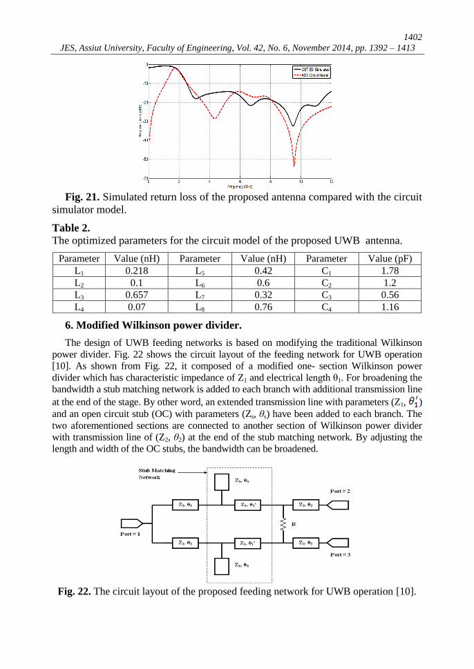
structure in CST microwave studio simulator. Fig.21 shows a simulated return loss of the
UWB patch antenna compared with the circuit simulator model. Table 2 shows the
optimized parameters for the equivalent circuit model of the proposed UWB antenna.
Fig. 20. The equivalent circuit of UWB circular proposed patch antenna
1402
JES, Assiut University, Faculty of Engineering, Vol. 42, No. 6, November 2014, pp. 1392 – 1413
Fig. 21. Simulated return loss of the proposed antenna compared with the circuit
simulator model.
Table 2.
The optimized parameters for the circuit model of the proposed UWB antenna.
Parameter Value (nH) Parameter Value (nH) Parameter Value (pF)
L1 0.218 L5 0.42 C1 1.78
L2 0.1 L6 0.6 C2 1.2
L3 0.657 L7 0.32 C3 0.56
L4 0.07 L8 0.76 C4 1.16
6. Modified Wilkinson power divider.
The design of UWB feeding networks is based on modifying the traditional Wilkinson
power divider. Fig. 22 shows the circuit layout of the feeding network for UWB operation
[10]. As shown from Fig. 22, it composed of a modified one- section Wilkinson power
divider which has characteristic impedance of Z1 and electrical length θ1. For broadening the
bandwidth a stub matching network is added to each branch with additional transmission line
at the end of the stage. By other word, an extended transmission line with parameters (Z1, )
and an open circuit stub (OC) with parameters (Zs, θs) have been added to each branch. The
two aforementioned sections are connected to another section of Wilkinson power divider
with transmission line of (Z2, θ2) at the end of the stub matching network. By adjusting the
length and width of the OC stubs, the bandwidth can be broadened.
Fig. 22. The circuit layout of the proposed feeding network for UWB operation [10].

1403
Gamal kassem et al., A proposed design of UWB monopole antenna and its linear arrays
First, a conventional Wilkinson power divider is designed with its center frequency f0 =
6.85 GHz and bandwidth ratio (fU/fL) equal 3.42 for covering the whole UWB frequency
range (3.1-10.6 GHz). It is shown from Fig. 22 that it consists of a modified two-section
Wilkinson power divider in [8] with removing the resistor of the second section R2. The
input and output impedance are chosen to be 50 Ω. Only one resistor is placed between the
output ports to prevent the signal transmission and obtain a good isolation between them.
According to the desired bandwidth ratio (m = fU/fL) the initial values for the divider
parameters Z1, θ1, Z2, θ2 and Bs can be determined by means of elementary transmission
line theory [9]. Then the length of the extended line is chosen arbitrarily to be different
than that of the main line ( ) to obtain more flexibility and degree of freedom and
hence the bandwidth can be enhanced. In order to get the values of Z1, Z2, Zs, θ1, θ2, and
Bs an even mode and odd mode analysis is derived in [4, 9, 10, 11] with removing the
resistor of the second section R2 using equations (1-5). The initial value of θ1 can be
calculated according to the operating bandwidth from equation (1) [9]:
(1)
(2)
(3)
n = 1 the frequency ratio between (1 < m < 3)
(4)
(5)
7. Single and double stage modified Wilkinson power divider.
The initial investigations of the proposed UWB feed network parameters were made
from summarized table 3. The proposed UWB feed network is designed on FR4 substrate
with dielectric substrate ɛr =4.5 and substrate height =1.5 mm. The overall size of proposed
UWB feed network is 23 x 19.5 mm2. The parameters of the proposed feed network were
optimized using CST-Microwave Studio to obtain a good reflection coefficient at all ports
and good isolation over the whole UWB frequency range. The final dimension of the
optimized parameters for the proposed feeding network is summarized in table 4.
Table 3.
The initial parameters of the proposed UWB feed network
Parameter Z1 θ1 Z2 θ2 Zs θs
Value 89 Ω 48.76o 27.1
o 61 Ω 137
o 52.1 Ω 11.2
o

1404
JES, Assiut University, Faculty of Engineering, Vol. 42, No. 6, November 2014, pp. 1392 – 1413
Table 4.
The optimized parameters of the proposed UWB feeding network.
Parameter W1 L1 W2 L2 Ws Ls
Value(mm) 0.67 2.18 2.015 1.98 10.12 2.63 0.55
The measured and simulated return loss at the input port (S11) in addition to, the
isolation between the output ports (S23) for the proposed feed network is shown in Fig. 23.
Fig. 24 shows the measured and simulated power division ratio at the output ports (S21,
S31). The return loss at the input port is reaches to -40.45 dB at the middle of the interesting
band and it reaches to 11.5 dB at the end of the band. The return losses at the output ports
reach to-12.5 dB at the frequency 8 GHz and reaches to -40 dB at the end of the band. It
can be seen that the power is divided equally between the output ports. The isolation
between the two outputs ports (S23 =S32) better than 12.8 dB at the start of the interesting
band (3.1 GHz) and better than 15.8 dB throughout the other frequency range.
Fig. 23. The measured and simulated return loss at the input port (S11) and the
isolation between the output ports (S23).
Fig. 24. The measured and simulated power ratio at the output ports (S21, S31).
As shown from Fig. 24 the values of measured and simulated power ratio at the output
ports (S21 and S31) are equal at the same frequency over the all range of frequencies.
However, these values (S21 and S31) at the start of frequency range are different from that at
the end of frequency range due to the use of FR4 material where the losses increased with
the increase the frequency. Fig. 25 shows the measured and simulated return loss at the
output ports (S22, S33).Two Cascaded Modified Wilkinson power Divider is shown in Fig.
26. The two cascaded modified WPD are used to excite 4x1 linear UWB antenna array.

1405
Gamal kassem et al., A proposed design of UWB monopole antenna and its linear arrays
The separating distance (d1 = 35 mm) between the each adjacent output port is assigned to
suitable to connect with the input microstrip transmission line of the UWB antenna array.
The simulated return loss at the input port (S11) and the isolation between the output ports
(S23, S34, S45) for the two cascaded modified Wilkinson power divider are shown in Fig. 27.
Fig. 28 shows the simulated return loss at the output ports (S22, S33, S44, and S55) for two
cascaded modified Wilkinson power divider. Fig. 29 shows the power ratios at the output
ports (S21, S31, S41, and S51) for two cascaded modified Wilkinson power divider. Also, ,
the difference between values of power ratios at the output ports (S21, S31, S41, and S51) at
the start of frequency range than that at the end of frequency range due to the use of FR4
material where the losses increased with the increase the frequency.
Fig. 25. The measured and simulated return loss at the output ports (S22, S33).
Fig. 26. Two Cascaded Modified Wilkinson power Divider
Fig. 27. The simulated return loss at the input (S11) and the isolation between the
output ports (S23, S34, S45) for two cascaded modified Wilkinson power
divider.

1406
JES, Assiut University, Faculty of Engineering, Vol. 42, No. 6, November 2014, pp. 1392 – 1413
Fig. 28. The simulated return loss at the output ports (S22, S33, S44, and S55) for
two cascaded modified Wilkinson power divider.
Fig. 29. The simulated power ratios at the output ports (S21, S31, S41, S51) for
two cascaded modified Wilkinson power divider.
8. Two element ultra-wide band linear antenna array
The two-element UWB linear antenna arrays is composed of UWB feed network circuit which
is previously designed and two UWB antenna elements. The geometry of the proposed two-element
linear antenna array prototypes is shown in Fig. 30. The spacing between the antenna elements has a
great effect on the overall performance of the array where the optimized value is 35 mm. Two
UWB antennas without power divider circuit have been studied in order to show the effect of the
distance between the antennas. Fig. 31 (a-c) shows the simulated return loss at the input of the two
antennas and the coupling between the antenna elements. The target here is to design a two-element
linear antenna arrays with good impedance matching characteristics across the desired UWB
frequency range. Moreover, the designed arrays should obtain higher gain, and stable radiation
patterns throughout the desired frequency band of interest. It has been found from the parametric
studies that using a rectangular cut in the common ground plane of dimensions (Wg and Lg) in the
two-element antenna array, the impedance matching of the antenna array is enhanced through the
UWB frequency range. This rectangular cut reduces the mutual coupling between the two antenna
elements. The optimized values for the rectangular cut in the common ground plane are: Wg= 5 mm
and Lg = 10.8 mm. The interspacing distance between the two antenna effects on the impedance
matching characteristic of the antenna and the grating lobe. The larger inter-element spacing, the
higher grating lobe will be occurred. The smaller inter-element spacing, the mutual coupling
between the two elements is increased as shown in Fig. 20. In case of d1=30 mm the two ground

1407
Gamal kassem et al., A proposed design of UWB monopole antenna and its linear arrays
planes of the two adjacent antennas are stuck (no rectangular cut between the two ground planes)
which is cause the coupling between them.
Fig. 30. The geometry of the proposed two-element linear antenna array prototypes
(a)
(b)
(c)
Fig. 31. The simulated return losses at the two antenna input ports: (a) S11 and
(b) S22 (c) The coupling between the two antenna elements at different distance
values (S21).

1408
JES, Assiut University, Faculty of Engineering, Vol. 42, No. 6, November 2014, pp. 1392 – 1413
The measured and simulated return loss curve for two elements antenna array
connected with its power divider circuit are shown in Fig. 32. Fig. 33 shows the gain and
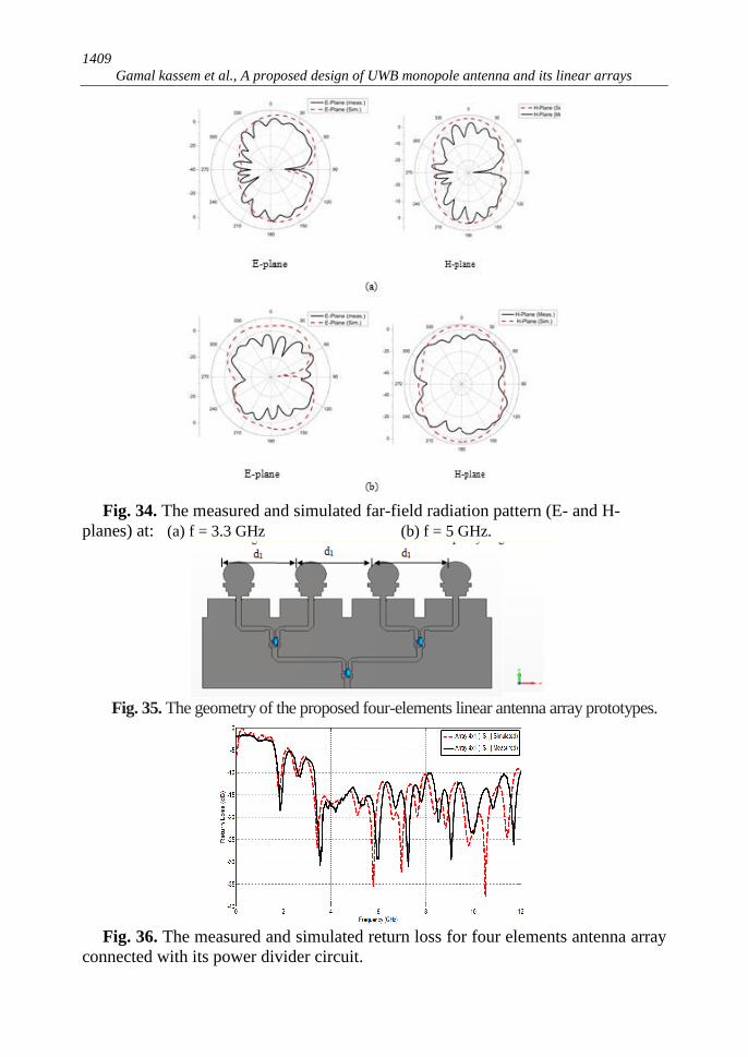
the directivity curves over the interesting bands of frequency. Fig. 34 shows the measured
and simulated far-field radiation pattern (E- plane and H-plane) at different values of
frequency (3.3 GHz and 5 GHz). The matching at frequency equal 3.3 GHz is -11 dB and
at frequency 5 GHz is -35 dB.
Fig. 32. The measured and simulated return loss for two elements antenna array
connected with its power divider circuit.
Fig. 33. The simulated gain and the directivity curves over the UWB frequency range.
9. Four elements ultra-wide band antenna array.
The four-element UWB linear antenna arrays is composed of UWB feed network
circuit which is previously designed and four UWB antenna elements. The geometry of the
proposed four-element linear antenna array prototypes is shown in Fig. 35. The target is to
design four-element linear antenna arrays with good impedance matching characteristics
across the desired UWB frequency range.
The measured and simulated return loss for four elements antenna array connected with
its power divider circuit is shown in Fig. 36. Fig. 37 shows the gain and the directivity
curves over the interesting bands of frequency where the target of using array is to increase
the gain. Fig. 38 shows the measured and simulated far-field radiation pattern (E- plane
and H-plane) at different values of frequency. It is clear from Fig. 38 that the beam is more
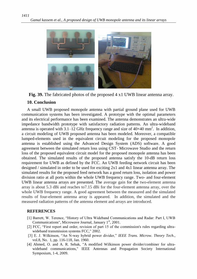
directive in the plane where the linear array is placed (Phi=0). Fig. 39 shows the fabricated
photos of the proposed 4 x1 UWB linear antenna array.
1409
Gamal kassem et al., A proposed design of UWB monopole antenna and its linear arrays
Fig. 34. The measured and simulated far-field radiation pattern (E- and H-
planes) at: (a) f = 3.3 GHz (b) f = 5 GHz.
Fig. 35. The geometry of the proposed four-elements linear antenna array prototypes.
Fig. 36. The measured and simulated return loss for four elements antenna array
connected with its power divider circuit.

1410
JES, Assiut University, Faculty of Engineering, Vol. 42, No. 6, November 2014, pp. 1392 – 1413
Fig. 37. The simulated gain and the directivity curves over the UWB frequency range.
Fig. 38. The measured and simulated far-field radiation pattern (E- plane and H-
plane) at: (a) f = 3.35 GHz (b) f = 7 GHz (c) f = 10 GHz
1411
Gamal kassem et al., A proposed design of UWB monopole antenna and its linear arrays
Fig. 39. The fabricated photos of the proposed 4 x1 UWB linear antenna array.
10. Conclusion
A small UWB proposed monopole antenna with partial ground plane used for UWB
communication systems has been investigated. A prototype with the optimal parameters
and its electrical performance has been examined. The antenna demonstrates an ultra-wide
impedance bandwidth prototype with satisfactory radiation patterns. An ultra-wideband
antenna is operated with 3.1–12 GHz frequency range and size of 40×40 mm2. In addition,
a circuit modeling of UWB proposed antenna has been modeled. Moreover, a compatible
lumped-elements used in the equivalent circuit modeling for the proposed monopole
antenna is established using the Advanced Design System (ADS) software. A good
agreement between the simulated return loss using CST- Microwave Studio and the return
loss of the proposed equivalent circuit model for the proposed monopole antenna has been
obtained. The simulated results of the proposed antenna satisfy the 10-dB return loss
requirement for UWB as defined by the FCC. An UWB feeding network circuit has been
designed / simulated in order to be used for exciting 2x1 and 4x1 linear antenna array. The
simulated results for the proposed feed network has a good return loss, isolation and power
division ratio at all ports within the whole UWB frequency range. Two- and four-element
UWB linear antenna arrays are presented. The average gain for the two-element antenna
array is about 5.3 dBi and reaches to7.15 dBi for the four-element antenna array, over the
whole UWB frequency range. A good agreement between the measured and the simulated
results of four-element antenna array is appeared. In addition, the simulated and the
measured radiation patterns of the antenna element and arrays are introduced.
REFERENCES
[1] Barrett, W. Terence, “History of Ultra Wideband Communications and Radar: Part I, UWB
Communications", Microwave Journal, January 1st, 2001.
[2] FCC, “First report and order, revision of part 15 of the commission's rules regarding ultra-
wideband transmission systems FCC," 2002.
[3] E. J. Wilkinson, “An N-way hybrid power divider,” IEEE Trans. Microw. Theory Tech.,
vol.8, No. 1, pp. 116-118, Jan. 1960.
[4] Ahmed, O. and A. R. Sebak, "A modified Wilkinson power divider/combiner for ultra-
wideband communications," IEEE Antennas and Propagation Society International
Symposium, 1-4, 2009.
Top view Bottom view

1412
JES, Assiut University, Faculty of Engineering, Vol. 42, No. 6, November 2014, pp. 1392 – 1413
[5] M. E. Bialkowski and A. M. Abbosh, “Design of a Compact UWB Out of-Phase Power
Divider,” IEEE Microw. Wireless Compon. Lett., vol. 17, No. 4, pp. 289-291, Apr. 2007.
[6] Yang, L. and Q.-X. Chu, "Design of a compact UWB Wilkinson power divider,"
International Conference on Microwave and Millimeter Wave Technology (ICMMT), Vol.
1, 360-362, 2008.
[7] Lin, Z. and Q.-X. Chu, 'A novel compact UWB power divider for spatial power combining,"
Journal of Electromagnetic Waves and Applications, Vol. 23, No. 13, 1803-1812, 2009.
[8] CST Microwave Studio Electromagnetic Field Simulation Soft-ware, Computer Simulation
Technology, Darmstadt, Germany. Progress In Electromagnetics Research C, Vol. 25, 2012.
[9] Zhou, B., H. Wang, and W.-X. Sheng, "A modified UWB Wilkin-son power divider using
delta stub," Progress In Electromagnetics Research Letters, Vol. 19, pp 49-55, 2010.
[10] R. Pazoki, M. R. Ghafouri Fard and H. Ghafouri Fard, “A Modification in the Single-Stage
Wilkinson Power Divider to Obtain Wider Bandwidth,” Proc. Asia-Pacific Microw, Conf.,
pp. 2325-2328, Dec. 2007.
[11] X.-P. Ou and Q.-X. Chu, “A Modified Two-section UWB Wilkinson Power Divider”,
International Conference on Microwave and Millimeter Wave Technology ( ICMMT) ,
China, vol.3, pp.1258-1260,April 21-29,2008.
[12] Sadat, S., M. Fardis, F. G. Gharakhili, and G. R. Dadashzadeh,"A compact microstrip
square-ring slot antenna for UWB applications," Progress In Electromagnetics Research,
Vol. 67, 173-179, 2007.
[13] Fallahi, R., A. A. Kalteh, and M. G. Roozbahani, "A novel UWB elliptical slot antenna with
band-notched characteristics, "Progress In Electromagnetics Research, Vol. 82, 127-136, 2008.
[14] Yin, X.-C., C.-L. Ruan, C.-Y. Ding, and J.-H. Chu, "A planar U type monopole antenna for
UWB applications," Progress In Electromagnetics Research Letters, Vol. 2, 1-10, 2008.
[15] Wang, H., H. Zhang, X. Liu, and K. Huang, "A CPW-FED ultra-wideband planar inverted
cone antenna," Progress In Electromagnetics Research C, Vol. 12, 101-112, 2010.
[16] Kumar, M., A. Basu, and S. K. Koul, "UWB printed slot antenna with improved
performance in time and frequency domains,"Progress In Electromagnetics Research C, Vol.
18, 197-210, 2011.
[17] Li, P., J. Liang, X. Chen, and C. Parini, "A 4-element ultra-wideband tapered- slot-fed
antenna array," IEEE Antennas and Propagation Society International Symposium, 4475-
4478, Jul. 9-14, 2006.
[18] SÄorgel, W., C. Sturm, and W. Wiesbeck, "Impulse responses of linear UWB antenna
arrays and the application to beam steering,"Proc. IEEE International Conference on Ultra-
wideband, 275-280,Sep. 2005.
[19] Liao, C.-H., P. Hsu, and D.-C. Chang, "Side lobe control of UWB antenna array for real
beam radar imaging," International Conference on Applications of Electromagnetism and
Student Innovation Competition Awards (AEM2C 2010), 284-288, Aug. 2010.
[20] Chen, M. and J. Wang, "Planar UWB antenna array with CPW feeding network,"
Proceedings of Asia-Pacific Microwave Conference (APMC 2008), 1-4, 2008.

1413
Gamal kassem et al., A proposed design of UWB monopole antenna and its linear arrays
"تصميم مقترح لهوائى أحادى القطبية على النطاق الترددى العريض ومصفوفاته الخطية"
لعربىملخص اال
-2.49تم عمل تصميم مقترح لهوائى صغير الحجم أحادى القطبية لكى يغطى النطاق الترددى العريض )
باستخدام نظام القطبيةاألحادى المقترح ميجا هرتز( ثم تم تصميم نموذج للدائرة المكافئة للهوائى 14.42
قياسات المحاكاة والقياسات المعملية لجميع تطابق بين التصميم المتقدم. تم تصنيع الهوائى المقترح وُوجد
اشعاعات المجال......الخ(. ولتصميم مصفوفة خطية ثنائية ورباعية -الكسب-بارامترات الهوائى )الفقد المرتد
لتوزيع القدرة على جميع الهوائيات بالتساوى وحتى اليحدث فقد فى للهوائى المقترح تم تصميم مجزئ القدرة
اإلشارات. كذلك تم تصنيع المصفوفات الثنائية والرباعية وُوجد تطابق بين قياسات المحاكاة والقياسات
-اشعاعات المجال-الكسب-)الفقد المرتد المعملية لجميع بارامترات المصفوفات الثنائية والرباعية
العزل......الخ(.
Related Documents