A Programmable Embedded Microprocessor for Bit-scalable In-memory Computing Hongyang Jia ([email protected] ), H. Valavi, Y. Tang, J. Zhang, N. Verma HotChips 2019 1

Welcome message from author
This document is posted to help you gain knowledge. Please leave a comment to let me know what you think about it! Share it to your friends and learn new things together.
Transcript

A Programmable Embedded Microprocessor for Bit-scalable In-memory Computing
Hongyang Jia ([email protected]),
H. Valavi, Y. Tang, J. Zhang, N. Verma
HotChips 2019 1

Memory
()
Digital Acceleration
MULT (INT8): 0.3pJ
MULT (INT32): 3pJMULT (FP32): 5pJ
MULT (INT4): 0.1pJ
Memory Size (𝑫𝑫)
En
erg
y p
er
Acc
ess
64b
Wo
rd (
pJ)
• … BUT, not data movement & memory accessing
Programmability overhead (instruction/operand fetch/decode)
Compute
>90% <10%
CPU
GPU
Accelerator(TPU)
1 5 10 50
Performance/Watt
• 10-100× gains in compute energy efficiency & speed
(https://cloud.google.com)
(45nm CMOS)
2
Typical Instruction Energy Breakdown

Focusing on Embedded Memory (SRAM)
• Even models for Edge AI can be large
(courtesy IBM)
• …BUT, reducing bit precision makes feasible to store on chip
28nm: <20mm2 embedded SRAM 16nm: <12mm2 embedded SRAM
Data Type Application Model # Params
Vision
Image
classificationResNet-50 26M
Object
detectionSSD300 24M
Language
Keyword
spotting
Deep
Speech 238M
Machine
translation
Base
Transformer50M
3

Outline
1. Basics of In-Memory Computing (IMC)• Amortizing data movement
2. IMC challenges• Compute SNR due to analog operation
3. High-SNR capacitor-based (charge-domain) IMC
4. Programmable heterogeneous IMC architecture• Bit-scalability, integration in memory space, near-memory data path
5. Prototype measurements• Chip measurements, SW libraries, neural-network demonstrations
4
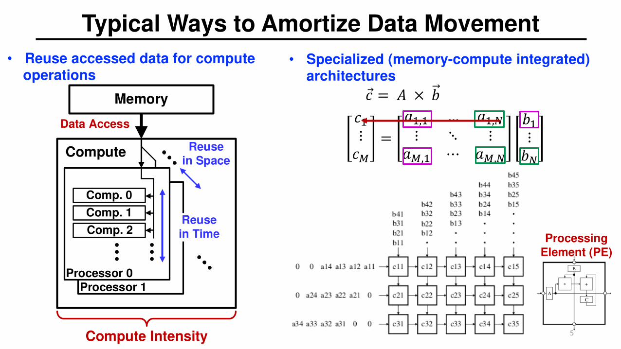
Typical Ways to Amortize Data Movement
• Specialized (memory-compute integrated) architectures𝑐𝑐1⋮𝑐𝑐𝑀𝑀 =
𝑎𝑎1,1 … 𝑎𝑎1,𝑁𝑁⋮ ⋱ ⋮𝑎𝑎𝑀𝑀,1 ⋯ 𝑎𝑎𝑀𝑀,𝑁𝑁𝑏𝑏1⋮𝑏𝑏𝑁𝑁
Processing Element (PE)
• Reuse accessed data for computeoperations 𝑐𝑐 = 𝐴𝐴 × 𝑏𝑏
5
Memory
Processor 0Processor 1
Comp. 0
Comp. 1
Comp. 2
Compute
Data Access
Reusein Time
Reusein Space
Compute Intensity

In-Memory Computing (IMC) to Amortize Data Movement
IMC Mode(row parallel)
SRAM Mode(row-by-row)
𝒃𝒃𝒄𝒄
[J. Zhang, VLSI’16][J. Zhang, JSSC’17]
𝑐𝑐1⋮𝑐𝑐𝑀𝑀 =
𝑎𝑎1,1 … 𝑎𝑎1,𝑁𝑁⋮ ⋱ ⋮𝑎𝑎𝑀𝑀,1 ⋯ 𝑎𝑎𝑀𝑀,𝑁𝑁𝑏𝑏1⋮𝑏𝑏𝑁𝑁
Digital output
Analog output
BL BLB
1 0
10
a1,1=-1
PRE
a1,N=+1
b1 →
bN →
(big)
(small)
𝑐𝑐 = 𝐴𝐴 × 𝑏𝑏 ⇒
→ Critical tradeoff: energy/throughput vs. SNR
6

Limited by Analog Computation
• Use analog circuits to ‘fit’ computation in bit cells⟶ Compute SNR limited by circuit non-idealities (nonlinearity, variation, noise)
WL
BL BLB
WLDAC
MA
MD
0 1.20.4 0.8
0
20
40
60
80
WL Voltage (V)
Bit
cell
Cu
rren
t (𝛍𝛍A) (10k-pt Monte Carlo sim.)
Nonlinearity
Variation
7

Where does IMC Stand Today?
Energy Efficiency (TOPS/W)
No
rmal
ized
Th
rou
gh
pu
t
(GO
PS
/mm
2 )
Bankman,
ISSCC’18, 28nm
Yuan, VLSI’18, 65nm
Moons, ISSCC’17, 28nm
Ando, VLSI’17, 65nm
Chen, ISSCC’16, 65nm Gonug,
ISSCC’18, 65nm
Biswas,
ISSCC’18, 65nm
Jiang,
VLSI’18, 65nm
10
10e2
10e3
10e4
Valavi, VLSI’18, 65nm
Khwa, ISSCC’18, 65nm
Zhang, VLSI’16, 130nm
Lee, ISSCC’18, 65nm
Shin, ISSCC’17, 65nm
Yin, VLSI’17, 65nm
10e-2 10e-1 1 10 10e2 10e3
Energy Efficiency (TOPS/W)
On
-ch
ip M
emo
ry S
ize
(kB
)
Yuan, VLSI’18, 65nm
10e3
10e2
10
1
10e-2 10e-1 1 10 10e2 10e3
Valavi,
VLSI’18, 65nm
Bankman,
ISSCC’18, 28nm
Lee, ISSCC’18,
65nm
Zhang,
VLSI’16,
130nmKhwa, ISSCC’18, 65nm
Jiang, VLSI’18,
65nm
Biswas, ISSCC’18, 65nm
Gonug, ISSCC’18, 65nm
Chen, ISSCC’16,
65nm
Yin, VLSI’17, 65nm
Ando, VLSI’17, 65nmMoons,
ISSCC’17,
28nm
IMC
Not IMC
• Potential for 10× higher energy efficiency & throughput
• … BUT, limited scalability (size, workloads, architectures)
8
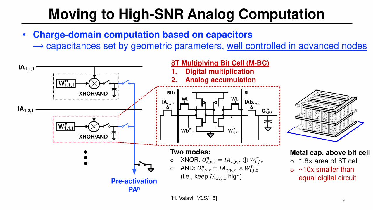
Moving to High-SNR Analog Computation
• Charge-domain computation based on capacitors⟶ capacitances set by geometric parameters, well controlled in advanced nodes
[H. Valavi, VLSI’18]
W1,1,1n
W1,1,1n
IA1,1,1
IA1,2,1
Pre-activation PAn
8T Multiplying Bit Cell (M-BC)1. Digital multiplication2. Analog accumulation
Two modes: o XNOR: 𝑂𝑂𝑥𝑥,𝑦𝑦,𝑧𝑧𝑛𝑛 = 𝐼𝐼𝐴𝐴𝑥𝑥,𝑦𝑦,𝑧𝑧 ⊕𝑊𝑊𝑖𝑖,𝑗𝑗,𝑧𝑧𝑛𝑛o AND: 𝑂𝑂𝑥𝑥,𝑦𝑦,𝑧𝑧𝑛𝑛 = 𝐼𝐼𝐴𝐴𝑥𝑥,𝑦𝑦,𝑧𝑧 × 𝑊𝑊𝑖𝑖,𝑗𝑗,𝑧𝑧𝑛𝑛
(i.e., keep 𝐼𝐼𝐴𝐴𝑥𝑥,𝑦𝑦,𝑧𝑧 high)
WLWLIAbx,y,z
Wbi,j,zn
Wi,j,zn
BL
Ox,y,zn
IAx,y,z
BLb
Metal cap. above bit cello 1.8× area of 6T cell
o ~10x smaller than
equal digital circuit
9
XNOR/AND
XNOR/AND

Previous Demonstration: 2.4Mb, 64-tile IMC
Moons,
ISSCC’17
Bang,
ISSCC’17
Ando,
VLSI’17
Bankman,
ISSCC’18
Valavi,
VLSI’18
Technology 28nm 40nm 65nm 28nm 65nm
Area (𝐦𝐦𝐦𝐦𝟐𝟐) 1.87 7.1 12 6 17.6
Operating VDD 1 0.63-0.9 0.55-10.8/0.8
(0.6/0.5)0.94/0.68/1.2
Bit precision 4-16b 6-32b 1b 1b 1b
on-chip Mem. 128kB 270kB 100kB 328kB 295kB
Throughput
(GOPS)400 108 1264 400 (60) 18,876
TOPS/W 10 0.384 6 532 (772) 866
• 10-layer CNN demos for MNIST/CIFAR-10/SVHN at energies of 0.8/3.55/3.55 μJ/image
• Equivalent performance to software implementation
[H. Valavi, VLSI’18]10

Need Programmable Heterogeneous Architectures
[B. Fleischer, VLSI’18]
General matrix multiplywith many elements (IMC)
Single/few-word operands(traditional, near-mem. acceleration)
• Matrix-vector multiply is only 70-90% of operations⟶ IMC must integrate in programmable, heterogenous architectures
11

Programmable IMC
CPU
(RISC-V)
AXI Bus
DMATimers GPIO UART
32
Program
Memory
(128 kB)
Boot-
loader
Data
Memory
(128 kB)
Compute-In-Memory
Unit (CIMU)
• 590 kb
• 16 bank
Ext.
Mem. I/F
Config.
Regs.
To E2PROM To DRAM Controller
Config
APB Bus 32
32
Tx Rx
8 13(data) (addr.)
32(data/addr.)
12
1. Interfaces to standard processor memory space2. Digital near-mem. accelerator (element compute)3. Bit scalability from 1 to 8 bits
w2b
Res
hap
ing
Bu
ffer
Inp
ut-
Vec
tor
Gen
erat
or
x
Ro
w D
eco
der
/ WL
Dri
vers
Memory Read/Write I/F
32b
8b
Near-Mem. Data Path
32b
AD
C
A
32b
Bit
Cell
Compute-In-
Memory Array
(CIMA)
f(y = A x)
AD
C

Bit-Parallel/Bit-Serial (BP/BS) Multi-bit IMC
10
20
30
40
6
10
14
18
2 3 4 5 6 7 8
2
4
6
BA
SQ
NR
(d
B)
Bx=2
Bx=4
Bx=8
N=2304, 2000, 1500, 1000, 500, 255
N=2304, 2000, 1500, 1000, 500, 255
N=2304, 2000, 1500, 1000, 500, 255
• SQNR different that standard INT compute- rounding effects are well modeled- SQNR is high at precisions of interest
13
N=2304
8-b SAR ADC(15|18% energy|areaoverhead)
Max. Dynamic Range: 2305
Dynamic Range: 256
1 1 0 1 0 0
AD
C
8b
x0[Bx-1:0] : 0-1-0
a0,0 a1,0
xN-1[Bx-1:0] : 0-0-0
x2303[Bx-1:0] : 1-1-0
[BA-1:0] [BA-1:0]
BX : Input-vector bit precision (E.g., 3b)
BA : Matrix bit precision (E.g., 3b)

Word-to-bit (w2b) Reshaping Buffer
Highly configurable connection network
Sequenced data for bit-serial compute
Circular interface for configurable convolutional striding
(Bx : Input-vector bit precision, E.g., 2b)
14
Reg.
File<0>
96b
72b
32b <0> <23>
Shifting
(conv.)
To Sparsity/AND-logic Controller
8b R
eg
8b R
eg
8b R
eg
8b R
eg
8b R
eg
8b R
eg
8b R
eg
8b R
eg
0[ ]1[ ]
0[ ]1[ ]
0[ ]1[ ]
0[ ]1[ ]
Reg.
File<7>
0[ ]1[ ]
0[ ]1[ ]
0[ ]1[ ]
0[ ]1[ ]
Sparsity-proportionalenergy savings
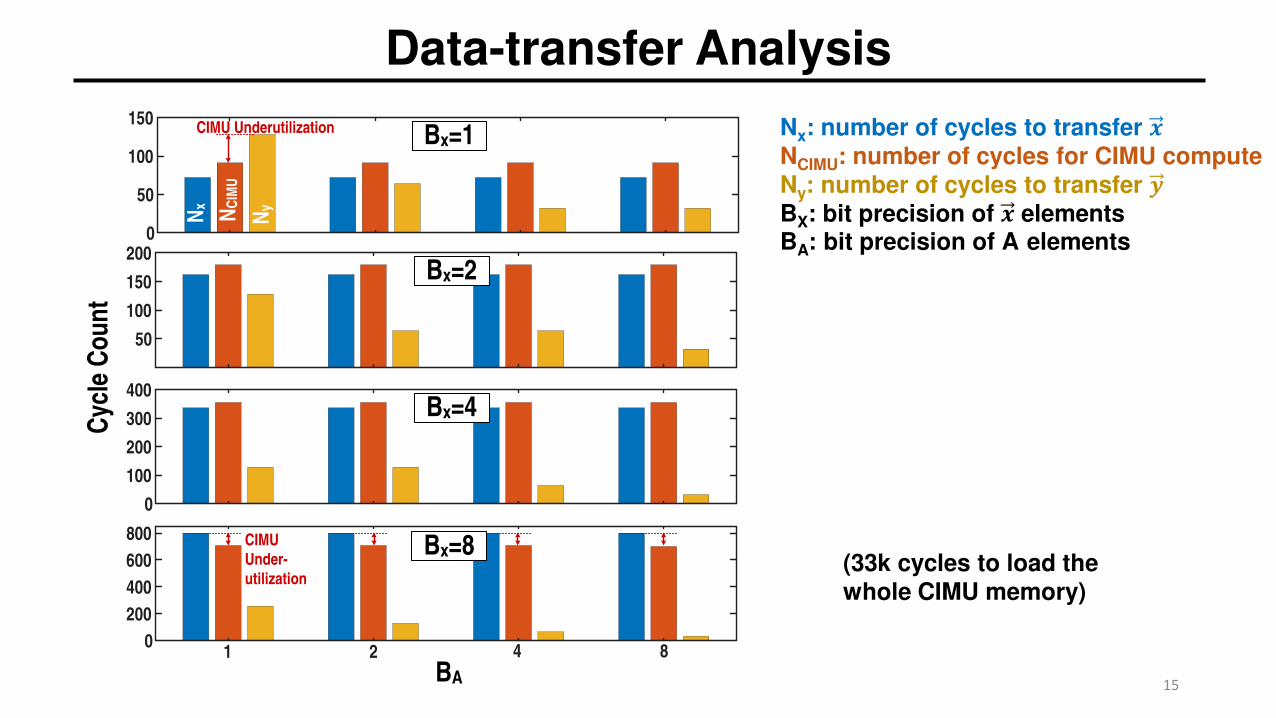
Data-transfer Analysis
0
50
100
150
50
100
150
200
0
100
200
300
400
Bx=1
Bx=2
Bx=4
0
200
400
600
800Bx=8
CIMU Underutilization
Nx
NC
IMU
Ny
CIMU
Under-
utilization
BA
1 2 4 8
Cyc
le C
ou
nt
Nx: number of cycles to transfer 𝒙𝒙NCIMU: number of cycles for CIMU computeNy: number of cycles to transfer 𝒚𝒚BX: bit precision of 𝒙𝒙 elementsBA: bit precision of A elements
15
(33k cycles to load the whole CIMU memory)

Near-memory Datapath (NMD)
Local
Scale
Local
Exp.
Global
Exp.
Global
Offset
9b
8b
19b 32b
32b
9b
Local
Offset
11b
ReLU Unit
8b ADC
Cross-column
mux’ing
BPBS Buffering
Non-linearfunctions
16

Prototype
DM
EM
PM
EM
CP
U AD
C
Te
st
Str
uc
t.
DM
A e
tc.
4×4CIMATiles
3m
m
4.5mm
Nea
r-m
em
. D
ata
pa
th
Technology (nm) 65
CIMU Area (mm2) 8.5
VDD (V) 1.2|0.85
On-chip mem. (kB) 74
Bit precision (b) 1-8
Thru.put (1b-GOPS/mm2) 0.26|0.10
Energy Eff. (1b-TOPS/W) 192|400
• Recent work has moved to advanced CMOS nodes⟶ Observe energy/density scaling like digital, while maintaining analog precision
17
Column Computation
0 1000 2000 3000 4000 5000
Ideal Pre-activation Value
0
50
100
150
200
250
AD
C O
utp
ut
Co
de
(Error bars show std.
deviation over 256 CIMA
columns)
8b ADC output
1Breakdown within CIMU accelerator
18
SummaryTech. (nm)VDD (V)
CPU
(pJ/instru)DMA
(pJ/32b-transfer)
Reshap. Buf.1
(pJ/32b-input)
FCLK (MHz)
Total area (mm2)
CIMA1
(pJ/column)ADC1
(pJ/column)
Dig. Datapath1
(pJ/output)
1.2 | 0.7/0.8565
52 | 26
13.5 | 7.0
35 | 12
13.5100 | 40
20.4 | 9.7
3.56 | 1.79
14.7 | 8.3
Energy Breakdown @VDD = 1.2V | 0.7V (P/D MEM, Reshap. Buf), 0.85V (rest)

Characterization and Demonstrations
Neural-Network Demonstrations
Network A
(4/4-b activations/weights)
Network B
(1/1-b activations/weights)
Accuracy of chip
(vs. ideal)
92.4%
(vs. 92.7%)
89.3%
(vs. 89.8%)
Energy/10-way
Class.1105.2 μJ 5.31 μJ
Throughput1 23 images/sec. 176 images/sec.
Neural Network
Topology
L1: 128 CONV3 – Batch norm
L2: 128 CONV3 – POOL – Batch norm.
L3: 256 CONV3 – Batch. norm
L4: 256 CONV3 – POOL – Batch norm.
L5: 256 CONV3 – Batch norm.
L6: 256 CONV3 – POOL – Batch norm.
L7-8: 1024 FC – Batch norm.
L9: 10 FC – Batch norm.
L1: 128 CONV3 – Batch Norm.
L2: 128 CONV3 – POOL – Batch Norm.
L3: 256 CONV3 – Batch Norm.
L4: 256 CONV3 – POOL – Batch Norm.
L5: 256 CONV3 – Batch Norm.
L6: 256 CONV3 – POOL – Batch Norm.
L7-8: 1024 FC – Batch norm.
L9: 10 FC – Batch norm.
CIFAR-10 Image Classification
19
2 4 6 8
2
4
6
8
2 4 6 85
10
15
20
SQ
NR
(d
B)
Multi-bit Matrix-Vector Multiplication
DX=1152Bit-true Sim.
DX=1152
MeasuredDX=1152DX=1152
Bx=2
BA
Bx=4
0 20 40 60 80-500
0
500
0 20 40 60 80-60
-40
-20
0
20
Data Index
Co
mp
ute
Val
ue
Bx=2, BA=2 Bx=4, BA=4
Bit True Sim.
Measured
BA
Data Index

Development board
To Host
Processor
20

Application-mapping Flows
NN Libs.Keras etc.
Int. Quant.
Chip Quant.Chip
Dev. SDKPython/Matlab
NN Layers
Chip Config.
Imp. SDKEmbedded C
NN Layers
Chip Config.
MVM
TrainingData
Params.
Runtime Ctrl.
User
DesignDeployment Flow
On-ChipHost Processor
Training Inference
Dev
. Flo
w
21

Training/Inference Libraries1. Deep-learning Training Libraries
(Keras)
2. Deep-learning Inference Libraries (Python, MATLAB, C)
Dense(units, ...)
Conv2D(filters, kernel_size, ...)
...
Standard Keras libs:
QuantizedDense(units, nb_input=4, nb_weight=4,
chip_quant=True, ...)
QuantizedConv2D(filters, kernel_size, nb_input=4,
nb_weight=4, chip_quant=True, ...)
...
QuantizedDense(units, nb_input=4, nb_weight=4,
chip_quant=False, ...)
QuantizedConv2D(filters, kernel_size, nb_input=4,
nb_weight=4, chip_quant=False, ...)
...
Custom libs:(INT/CHIP quant.)
chip_mode = True
outputs = QuantizedConv2D(inputs,
weights, biases, layer_params)
outputs = BatchNormalization(inputs,
layer_params)
...
High-level network build (Python):
Embedded C:
Function calls to chip (Python):
chip.load_config(num_tiles, nb_input=4,
nb_weight=4)
chip.load_weights(weights2load)
chip.load_image(image2load)
outputs = chip.image_filter()
chip_command = get_uart_word();
chip_config();
load_weights(); load_image();
image_filter(chip_command);
read_dotprod_result(image_filter_command);22

Conclusions
Matrix-vector multiplies (MVMs) are a little different than other computations⟶ high-dimensionality operands lead to data movement / memory accessing
Capacitor-based IMC enables high-SNR analog compute⟶ enables scale and robust functional specification of IMC for architectural design
Programmable IMC is demonstrated (with supporting SW libraries)⟶ physical IMC tradeoffs will drive specialized mapping/virtualization algorithms
Acknowledgements: funding provided by ADI, DARPA, NRO23
Resent work has moved to advanced nodes⟶ energy and density scaling similar to standard digital logic

Backup
24
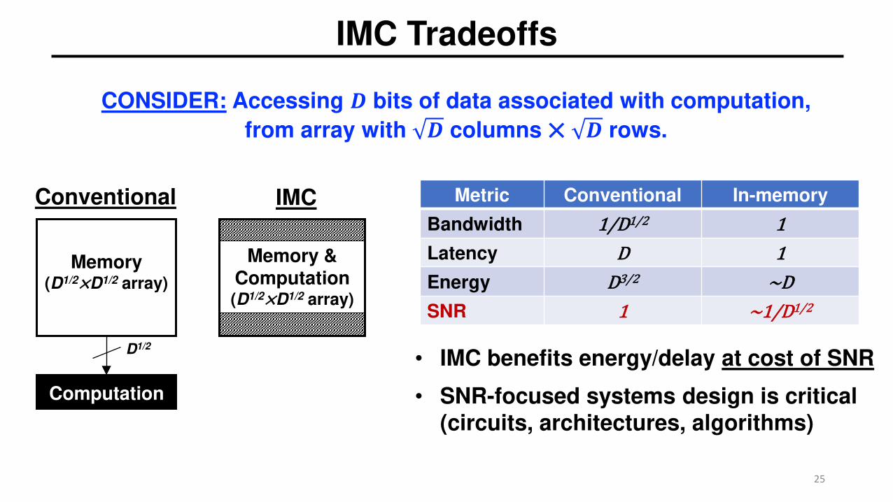
IMC Tradeoffs
CONSIDER: Accessing 𝑫𝑫 bits of data associated with computation,
from array with 𝑫𝑫 columns ⨉ 𝑫𝑫 rows.
Memory(D1/2×D1/2 array)
Computation
Memory &Computation(D1/2×D1/2 array)
D1/2
Conventional IMC Metric Conventional In-memory
Bandwidth 1/D1/2 1
Latency D 1
Energy D3/2 ~D
SNR 1 ~1/D1/2
• IMC benefits energy/delay at cost of SNR
• SNR-focused systems design is critical (circuits, architectures, algorithms)
25

Algorithmic Co-design(?)
••
• • ••• •• ••
•••••
•
WEAK classifier K
WEAK classifier 2Weighted
Voter
Classifier
Trainer
WEAK classifier 1
Feature 1
Fe
atu
re 2
••
• • ••• •• ••
•••••
•
••
• • ••• •
• ••
••••••
••
• • ••• •• ••
•••••
•
• Chip-specific weight tuning
[Z. Wang, TVLSI’15]
[Z. Wang, TCAS-I’15]
[S. Gonu., ISSCC’18]
• Chip-generalized weight tuning
G gi
Training InferenceParameters𝜃𝜃(𝑥𝑥,𝐺𝐺,ℒ)
Normalized MRAM cell standard dev.1 2 3 4 5 6 7 8 9 1010
2030405060708090
100
Acc
ura
cy
L = |𝑦𝑦 − �𝑦𝑦(𝑥𝑥,𝜃𝜃)|2L = |𝑦𝑦 − �𝑦𝑦(𝑥𝑥,𝜃𝜃,𝐺𝐺)|2
E.g.: BNN Model (applied to CIFAR-10)
[B. Zhang, ICASSP 2019]26

M-BC Layout
2fF:
1fF:
0.5fF:
E.g., MOM-capacitor matching (130nm):
[H. Omran, TCAS-I’16]
WL
BLGND
GND
WL
BLb
VDD
VDD
GND (shield)
VDD
GND
BLBLb
VDD
GND
𝑰𝑰𝑰𝑰𝒙𝒙,𝒚𝒚,𝒛𝒛𝑰𝑰𝑰𝑰𝒃𝒃𝒙𝒙,𝒚𝒚,𝒛𝒛
WL(6T area: 1.0 A.U.) (M-BC area: 1.8 A.U.)
GN
D
• >14-b capacitor matching across M-BCs
• >14k IMC rows for matching-limited SNR
[H. Valavi, VLSI’18]
27
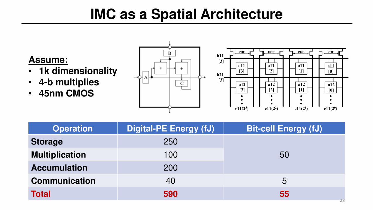
IMC as a Spatial Architecture
Operation Digital-PE Energy (fJ) Bit-cell Energy (fJ)
Storage 250
50Multiplication 100
Accumulation 200
Communication 40 5
Total 590 55
Assume:• 1k dimensionality• 4-b multiplies• 45nm CMOS
PRE
c11(23)
PRE PRE PRE
a11
[3]
b11
[3]a11
[2]
a11
[1]
a11
[0]
a12
[3]
a12
[2]
a12
[1]
a12
[0]
b21
[3]
c11(22) c11(21) c11(20)
28

Application mapping
• IMC engines must be ‘virtualized’⟶ IMC amortizes MVM costs, not weight loading ⟶ Need new mapping algorithms (physical tradeoffs very diff. than digital engines)
(output activations)
𝑾𝑾𝒊𝒊,𝒋𝒋,𝒛𝒛𝒏𝒏(N - I⨉J⨉Z filters)
𝑰𝑰𝑰𝑰𝒙𝒙,𝒚𝒚,𝒛𝒛(X⨉Y⨉Z input
activations)
• EDRAM→IMC/4-bit: 40pJ
• Reuse: 𝑁𝑁 × 𝐼𝐼 × 𝐽𝐽 (10-20 lyrs
• EMAC,4-b: 50fJ
Activation Accessing:Weight Accessing:
• EDRAM→IMC/4-bit: 40pJ
• Reuse: 𝑋𝑋 × 𝑌𝑌• EMAC,4-b:50fJ
Reuse ≈ 1k
MemoryBound
ComputeBound
Ex.: X⨉Y sets reuse of filter weights
29
Related Documents