954 IEEEJOURNAL OFSOLID-STATECIRCUITS,VOL.SC-22,NO. 6, DECEMBER 1987 A Pipelined 5-Msample/s 9-bit Analog-to-Digital Converter STEPHEN H. LEWIS ANDPAUL R. GRAY, FELLOW,IEEE ,Ost?act —A pipelined, 5-Msample/s, 9-bit anafog-to-digital (A/~) con- verter with digital correction has been designed and fabricated in 3-pm CMOS technology. It requires 8500 mi12, consumes 180 mW, and has an input capacitance of 3 pF. A fully differential architecture is used only a two-phase nonoverlapping clock is required, and an on-chip sample-and-hold (S/H) amplifier is included. I. INTRODUCTION T RADITIONAL designs of high-speed CMOS analog- to-digital (A/D) converters have used parallel (flash) architectures [1]–[13]. While flash architectures usually yield the highest throughput rate, they tend to require large silicon. areas because of the many comparators required. An important objective is the realization of high-speed A/D converters in much less area than that required by flash converters so that the A/D interface function can be integrated on the same chip with associ- ated complex, high-speed, image-processing functions. Multistage conversion architectures reduce the required area by reducing the total number of comparators [14]–[19]. Using a pipelined mode of operation in these architectures allows the stages to operate concurrently and makes the maximum throughput rate almost independent of the num- ber of stages. Also, digital correction techniques signifi- cantly reduce the sensitivity of the architecture to certain component nonidealities. Pipelined configurations have been previously applied in high-performance board-level converters, but they have not been applied to monolithic CMOS A/D converters because of the difficulty of realiz- ing high-speed interstage sample-and-hold (S/H) gain functions in CMOS technologies. In this paper, an experi- mental four-stage pipelined A/D converter with digital correction that has 9-bit resolution and 5-Msample/s con- version rate in a 3-pm CMOS technology is described. The experimental converter uses high-speed differential switched-capacitor circuitry to carry out the interstage gain functions. This paper is divided into four additional parts. In Section II, pipelined A/D architectures are described con- Manuscript received May 8, 1987; revised July 24, 1987. This work was supported by DARPA under Contract NOOO39-C-O1O7 and by the Na- tional Science Foundation under Contract DCI-8603430. The authors are with the Electronics Research Laboratory, University of California, Berkeley, CA 94720. IEEE Log Number 8716973. ceptually, and their advantages over llasn ana two-step subranging architectures [17] are explained. In Section III, the error sources present in pipelined A/D converters are identified, and the way in which digital correction eliminates the effects of some of these errors is shown. In Section IV, the circuits in an experimental prototype are described. Finally, experimental results from the prototype converters are given in Section V. II. CONCEPTUALDESCRIPTION A block diagram of a general pipelined A/D converter with k stages is shown in Fig. 1. Each stage contains an S/H circuit, a low-resolution A/D subconverter, a low- resolution digital-to-analog (D/A) converter, and a dif- ferencing fixed-gain amplifier. In operation, each stage initially samples and holds the output from the previous stage. Each stage then does a low-resolution A/D conver- sion on the held input, and the code just produced is converted back into an analog signal by a D/A converter. Finally, the D/A converter output is subtracted from the held input, producing a residue that is amplified and sent to the next stage. The primary potential advantages of the pipelined archi- tecture are high throughput rate and low hardware cost. The high throughput rate of the pipelined architecture stems from concurrent operation of the stages. At any time, the first stage operates on the most recent sample, while the next stage operates on the residue from the previous sample, and so forth. If the A/D subconversions are done with flash converters, a pipelined architecture only needs two clock phases per conversion. Flash archi- tectures also require two clock phases per conversion, one each for sampling and A/D conversion, and use pipelining to do the digital decoding operation. The throughput rate of flash converters is maximized because their pipelined information is entirely digital and can be transferred to l-bit accuracy in less time than it takes to generate and transfer the analog residue in a pipelined multistage archi- tecture. The area and consequent manufacturing cost of pipelined converters is small compared to those of flash converters, however, because pipelined converters require fewer comparators than flash converters. For example, the 9-bit prototype pipelined converter described in Section IV 0018-9200/’87/1200-0954$01.00 01987 IEEE

Welcome message from author
This document is posted to help you gain knowledge. Please leave a comment to let me know what you think about it! Share it to your friends and learn new things together.
Transcript

954 IEEEJOURNAL OF SOLID-STATECIRCUITS,VOL. SC-22,NO. 6, DECEMBER 1987
A Pipelined 5-Msample/s 9-bitAnalog-to-Digital Converter
STEPHEN H. LEWIS ANDPAUL R. GRAY, FELLOW,IEEE
,Ost?act —A pipelined, 5-Msample/s, 9-bit anafog-to-digital (A/~) con-verter with digital correction has been designed and fabricated in 3-pmCMOS technology. It requires 8500 mi12, consumes 180 mW, and has aninput capacitance of 3 pF. A fully differential architecture is used only a
two-phase nonoverlapping clock is required, and an on-chip sample-and-hold(S/H) amplifier is included.
I. INTRODUCTION
T RADITIONAL designs of high-speed CMOS analog-to-digital (A/D) converters have used parallel (flash)
architectures [1]–[13]. While flash architectures usuallyyield the highest throughput rate, they tend to requirelarge silicon. areas because of the many comparatorsrequired. An important objective is the realization ofhigh-speed A/D converters in much less area than thatrequired by flash converters so that the A/D interfacefunction can be integrated on the same chip with associ-ated complex, high-speed, image-processing functions.Multistage conversion architectures reduce the requiredarea by reducing the total number of comparators [14]–[19].Using a pipelined mode of operation in these architecturesallows the stages to operate concurrently and makes themaximum throughput rate almost independent of the num-ber of stages. Also, digital correction techniques signifi-cantly reduce the sensitivity of the architecture to certaincomponent nonidealities. Pipelined configurations havebeen previously applied in high-performance board-levelconverters, but they have not been applied to monolithicCMOS A/D converters because of the difficulty of realiz-ing high-speed interstage sample-and-hold (S/H) gainfunctions in CMOS technologies. In this paper, an experi-mental four-stage pipelined A/D converter with digitalcorrection that has 9-bit resolution and 5-Msample/s con-version rate in a 3-pm CMOS technology is described.The experimental converter uses high-speed differentialswitched-capacitor circuitry to carry out the interstage gainfunctions.
This paper is divided into four additional parts. InSection II, pipelined A/D architectures are described con-
Manuscript received May 8, 1987; revised July 24, 1987. This work wassupported by DARPA under Contract NOOO39-C-O1O7 and by the Na-tional Science Foundation under Contract DCI-8603430.
The authors are with the Electronics Research Laboratory, Universityof California, Berkeley, CA 94720.
IEEE Log Number 8716973.
ceptually, and their advantages over llasn ana two-stepsubranging architectures [17] are explained. In Section III,the error sources present in pipelined A/D converters areidentified, and the way in which digital correctioneliminates the effects of some of these errors is shown. InSection IV, the circuits in an experimental prototype aredescribed. Finally, experimental results from the prototypeconverters are given in Section V.
II. CONCEPTUALDESCRIPTION
A block diagram of a general pipelined A/D converterwith k stages is shown in Fig. 1. Each stage contains anS/H circuit, a low-resolution A/D subconverter, a low-resolution digital-to-analog (D/A) converter, and a dif-ferencing fixed-gain amplifier. In operation, each stageinitially samples and holds the output from the previousstage. Each stage then does a low-resolution A/D conver-sion on the held input, and the code just produced isconverted back into an analog signal by a D/A converter.Finally, the D/A converter output is subtracted from theheld input, producing a residue that is amplified and sentto the next stage.
The primary potential advantages of the pipelined archi-tecture are high throughput rate and low hardware cost.The high throughput rate of the pipelined architecturestems from concurrent operation of the stages. At anytime, the first stage operates on the most recent sample,while the next stage operates on the residue from theprevious sample, and so forth. If the A/D subconversionsare done with flash converters, a pipelined architectureonly needs two clock phases per conversion. Flash archi-tectures also require two clock phases per conversion, oneeach for sampling and A/D conversion, and use pipeliningto do the digital decoding operation. The throughput rateof flash converters is maximized because their pipelinedinformation is entirely digital and can be transferred tol-bit accuracy in less time than it takes to generate andtransfer the analog residue in a pipelined multistage archi-tecture. The area and consequent manufacturing cost ofpipelined converters is small compared to those of flashconverters, however, because pipelined converters requirefewer comparators than flash converters. For example, the9-bit prototype pipelined converter described in Section IV
0018-9200/’87/1200-0954$01.00 01987 IEEE

LEWISAND GRAY: PIPELINED5-MSAMPLE/S9-BITANALOC+-TO-LXGITAI_CONVERTER 955
‘%T-F3”””-E3nl bits n2 bits nk bits
Residue
1
g
INS/H ‘+
~nl
m bit nl bitADC I DAC
unl bits
Fig. 1. Block diagram of a general pipelined A/D converter
uses 28 comparators and requires a core area of 8500mi12 in a 3-pm CMOS technology. A 9-bit flash converterwould use 512 comparators and would be more than tentimes larger than the pipelined prototype in the sametechnology. Not only is the area small for pipelined con-verters, but also it is linearly related to the resolutionbecause if the necessary accuracy can be achieved throughcalibration or trimming, the resolution can be increased byadding stages to the end of the pipeline without increasingthe number of clock phases required per conversion. Incontrast, flash and subranging architectures need exponen-tial, rather than linear, increases in area to increase theirresolution and also require trimming or calibration forgreater than 8- or 9-bit linearity.
Other advantages of the pipelined architecture stemfrom the use of S/H amplifiers to isolate the stages. First,because an S/H amplifier can also be used on the input ofthe A/D converter, pipelined architectures can accuratelysample high-frequency input signals. Second, the interstagegains from these amplifiers diminish the effects of non-idealities in all stages after the first stage on the linearity ofthe entire conversion; furthermore, this allows the con-verter to use a digital correction technique in which non-linearity in the A/D subconversions has little effect on theoverall linearity. This subject is presented in Section III.
The main disadvantage of pipelined A/D converters isthat they require the use of operational amplifiers (opamps) to realize parasitic-insensitive S/H amplifiers. Al-though the S/H amplifiers improve many aspects of theconverter performance, the op amps within the S/Hamplifiers limit the speed of the pipelined converters. Incontrast, op amps are not required in subranging architec-tures. Because high-speed op amps are difficult to realize, acommon goal in the design of subranging A/D convertersis to avoid using op amps. If op amps are not used,however, it is impossible to realize, parasitic-insensitiveS/H amplifiers. The consequent high-frequency inputsampling is poor, stage operation is sequential, and toler-ance to error sources in stages after the first is unimprovedfrom that of the first stage. Also, flash converters usuallydo not use an input S/H amplifier because ,of the diffi-culty in realizing an op amp in CMOS technologies that isfast enough to drive the inherently large input load. There-fore, flash converters often suffer reduced performance athigh input signal frequencies.
Fig. 2.
The
Gain :
IN
mnl-bit nl -bitADC I DAC
{1nl bits
un2-bitADC
n2 bits
Block diagram of a two-stage pipelined A/D converter withoffset and gain errors.
III. ERROR SOURCES
primary error sources present in a pipelined A/D. .converter are offset errors in the S/H circuits and ampli-fiers, gain errors in the S/H circuits and amplifiers, A/Dsubconverter nonlinearity, D/A subconverter nonlinearity,and op-amp settling-time errors. With digital correction, asshown below, the effects of offset, gain, and A/D subcon-verter nonlinearity are reduced or eliminated; therefore,the D/A converter nonlinearity and op-amp settling-timeerrors limit the performance of pipelined A/D converters.To begin the error analysis, the effects of offset and gainerrors are considered next.
A block diagram of a two-stage pipelined A/D con-verter with offset and gain errors in each of the S/Hcircuits and the interstage amplifier is shown as a repre-sentative example in Fig. 2. The nonideal S/H circuits andinterstage amplifier are replaced by ideal elements in serieswith gain and offset errors, and each of these replacementsis surrounded by a dotted line. The gain error in thefirst-stage S/H circuit changes the conversion range of theA/D converter and does not affect linearity. The gainerrors in the interstage amplifier and second-stage S/Hcircuit can be combined into one equivalent error that doesaffect linearity. However, because the interstage gain onlyhas to be accurate enough to preserve the linearity of thestages after the first stage, the effect of this gain error onlinearity is small. For example, if both stages in Fig, 2 have4-bit resolution, and if the only error is in the gain of theinterstage amplifier, the interstage amplifier gain should beequal to 16 and must be accurate to within + 3 percent.
The offset error in the first-stage S/H circuit causes aninput-referred offset but does not affect linearity. Theoffset errors in the interstage amplifier and second-stageS/H circuit can be combined into one equivalent offsetthat does not affect linearity if digital correction is used.Because addition is commutative, the equivalent offset canbe pushed to the left of the first-stage subtracter. To movethe equivalent offset to the input branch, where is causesan input-referred offset, an equal but opposite offset mustbe inserted in the first-stage A/D subconverter branch. Asshown below, the effect of the offset in the first-stage A/Dsubconverter is eliminated by the digital correction.
Next, the effect of nonlinearity in the first-stage A/Dsubconversion is considered. A block diagram of one stagein a pipelined A/D converter is shown in Fig. 3(a). A 2-bitstage is used as a representative example. Nonlinearity in

956 IEEEJOURNALOFSOLID-STATECIRCUITS,VOL.SC-22,NO. 6, DECEMBER1987
Residue
++14
‘E
Vinw+
Input ; -ReferredLinearity + :
Error
2-bit 2-bitADC DAC
I2 bits
(a)
ResidueA
00 ; 01 lo~lll/2LsB -
0/<:.1 . . . . . . . . . . .
Conv. RangeVin of Next Stage
-1/2 LSB -
Fig. 3, (a)converter.
(b)
Residue
w“’”””””,~~B o, 01 i 10 11,
1/2 LS,B ~......... ........ . ...
0Conv”. Range
Vin...of NxtStagege-1/2LsB ----- ““””““””””‘ I
-1 LSB ;,l— -
Negative Decision Positive DecisionLevel Error Level Error
(c)
Block diagram of one 2-bit stage in a pipelined A/D(b) Ideal residue versus input. (c) Residue versus input with
A/D subconverter nonlinearity.
the A/D subconverter is modeled as an input-referredlinearity error. The effect of this nonlinearity is studied byexamining plots of the residue versus the input. Two suchplots are shown in Fig. 3(b) and (c).
In Fig. 3(b), both the A/Dsubconverter andthe D/Aconverter are assumed to be ideal. The plot has a sawtoothshape because when the input is between the decisionlevels determined by the A/D subconverter, the A/Dsubconverter and D/A converter outputs are constant;therefore, the residue rises with the input. When the inputcrosses a decision level, the A/D subconverter and D/Aconverter outputs increase by one least significant bit(LSB) at a 2-bit level, so the residue decreases by 1 LSB.Here, the residue is always between f 1/2 LSB and con-sists only of the part of the input that is not quantized bythe first stage. With the interstage gain equal to 4, themaximum residue is amplified into a full-scale input to thenext stage; therefore, the conversion range of the nextstage is equal to the maximum residue out of the firststage.
A similar curve is shown in Fig. 3(c) for a case when theA/D subconverter has some nonlinearity, but the D/Aconverter is still ideal. In this example, two of the A/Dsubconverter decision levels are shifted, one by – 1/2 LSBand the other by + 1/2 LSB. When the input crosses ashifted decision level, the residue decreases by 1 LSB. Ifthe decision levels are shifted by less than 1/2 LSB, theresidue is always between + 1 LSB. Here, the residueconsists of both the unquarttized part of the input and theerror caused by the A/D subconverter nonlinearity. Be-
~ Stage1 Stage 2
n2 bit Ereg
y Correction
: nl bit E Logicreg
,,, .,nl+n2-1
outputs
Fig. 4. Block diagram of a two-stage pipelined A/D converter withdigital correction.
cause the D/A converter is assumed to be ideal, theseincreased residues are accurate for the codes to which theycorrespond; therefore, at this point, no information is lost.If the interstage gain is still 4, however, information is lostwhen the larger residues saturate the next stage and pro-duce missing codes in the conversion. Therefore, if theconversion range of the second stage is increased to handlethe larger residues, they can be encoded and the errorscorrected. This process is called digital correction [20], [21]and is described next.
A block diagram of a two-stage pipelined A/D con-verter with digital correction is shown in Fig. 4. The newelements in this diagram are the pipelined latches, thedigital correction logic circuit, and the amplifier with again of 0.5. The amplifier with a gain of 0.5 is conceptualonly and is drawn to show that the interstage gain isreduced by a factor of 2 so that nonlinearity error in anamount between f 1/2 LSB at a nl-bit level in the first-stage A/D subconversion does not produce residues thatsaturate the second stage. If the first stage is perfectlylinear, only half the conversion range of the second stage isused. Therefore, 1 bit from the second stage is saved todigitally correct the outputs from the first stage; the othern 2-1 bits from the second stage are added to the overallresolution. After the pipelined latches align the outputs intime so that they correspond to one input, the digitalcorrection block detects overrange in the outputs of thesecond stage and changes the output of the first stage by 1LSB at a nl-bit level if overrange occurs. Digital correc-tion improves linearity by allowing the converter to post-pone decisions on inputs that are near the first-stage A/Dsubconverter decision levels until the residues from theseinputs are amplified to the point where similar nonlinear-ity in later-stage A/D subconverters is insignificant.
To do the digital correction, a correction logic circuit isrequired. Also, if flash converters are used in the stages, allstages after the first require twice as many comparators aswithout digital correction. The logic is simple, however,and none the comparators needs to be offset canceled.
It is shown above that with digital correction, nonlinear-ity in the A/D subconverters can be corrected if the D/Aconverter is ideal. Therefore, the D/A converter in thefirst stage determines the linearity of the entire A/Dconverter. Such D/A converters can be realized with resis-tor strings for Iinearities in the 8–9-bit range. For integrallinearity greater than 9 bits, the design of such a D/Aconverter is not trivial and either requires calibration or
trimming. Also, fast settling op amps are reqvired to doanalog subtraction and amplification at the sampling rateof the A/D converter. The 3-pm CMOS prototype de-scribed in Section IV is able to do these functions at 5Msample/s. The maximum speed of such processing in-creases in scaled technologies, and video conversion ratesshould be achievable in 1.5–2-pm CMOS technologies.
IV. PROTOTYPE
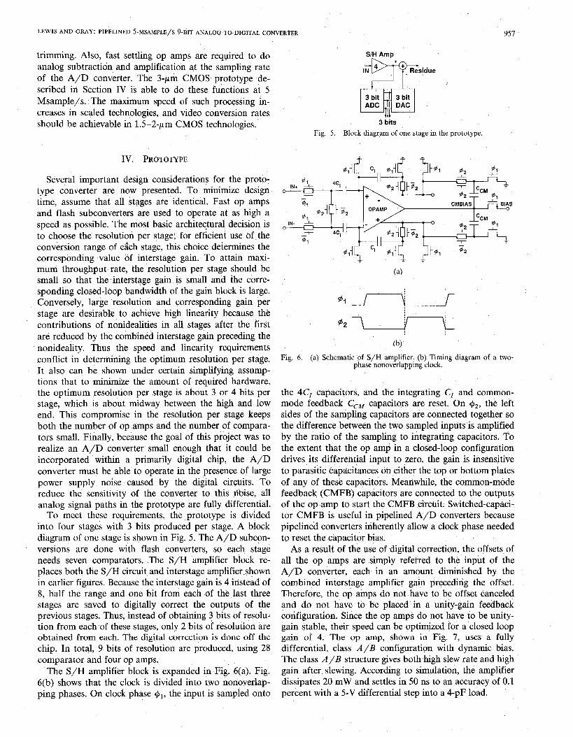
Several important design considerations for the proto-type converter are now presented. To minimize designtime, assume that all stages are identical. Fast op ampsand flash subconverters are used to operate at as high aspeed as possible. The mcist basic architectural decision isto choose the resolution per stage; for efficient use of theconversion range of each stage, this choice determines thecorresponding value of interstage gain. To attain mmii-mum throughput rate, the resolution “per stage should besmall so that the interstate gain is small and the corre-sponding closed-loop bandwidth of the gain block is large.Conversely, large ‘resolution and corresponding gain perstage are desirable to achieve high linearity because thecontributions of nonidealities in all stages after the i’irstare reduced by the combined interstage gain preceding thenonidealit y. Thus the speed and linearity requirementsconflict in determinifig the optimum resolution per stage.It also can be shown under certain simplifying assump-tions that to minimize the amount of required hardware,the optimum resolution per stage is about 3 or 4 bits perstage, which is about midway between the high and lowend. This compromise in the resolution per stage keepsboth the number of op amps and the number of compara-tors small. Finally, because the goal of this project was torealize an A/D converter small enough that it could beincorporated within a primarily digital chip, the A/Dconverter must be able to operate in the presence bf largepower supply noise caused by the digital circttits. Toreduce the sensitivity of the converter to this @ise, allanalog signal paths in the prototype are fully differential.
To meet these requirements, the prototype is dividedinto four stages with 3 bits produced per stage. A blockdiagram of one stage is shown in Fig. 5. The A/D subcon-versions are done with flash converters, so each stageneeds seven comparators. The S/H amplifier block re-places both the S/H circuit and interstage amplifier shownin earlier figures. Because the interstage gain is 4 instead of8, half the range and one bit from each of the last threestages are saved to digitally correct the outputs of theprevious stages. Thus, instead of obtaining 3 bits of resolu-tion from each of these stages, only 2 bits of resolution areobtained from each. The digital correction is done off thechip. In total, 9 bits of resolution are produced, using 28comparator and four op amps. ,,
The S/H amplifier block is expanded in Fig. 6(a). Fig.6(b) shows that the clock is divided into two nonoverlap-ping phases. On clock phase 1#1,the input is sampled onto
957
SIH Amp
3
+
IN 4+
. Residue
3 bit 3 bitADC I DAC
13 bits
Fig. 5. Block diagram of one stage in the protot~e.
‘#,
31
?1
%L cl” %i~ Jt@l 32
(a)
(b)
Fig. 6. (a) Schematic of S/H amplifier. (b) Timing diagram of a two-phase nonoverlapping clock.
the 4C1 capacitors, and the integrating C1 and common-mode feedback C~&fcapacitors are reset. On Oz, the leftsides of the sampling capacitors are connected together sothe difference between the two sampled inputs is amplifiedby the ratio of the sampling to integrating capacitors. Tothe extent that the op amp in a closed-loop configurationdrives its differential input to zero, the gain is insensitiveto parasitic ~ap~citances on either the top or bottom platesof any of these capacitors. Meanwhile, the common-modefeedback (CMFB) capacitors are connected to the outputsof the op amp to start the CMFB circuit. Switched-capaci-tor CMFB is useful in pipelined A/D converters becausepipelined converters inherently allow a clock phase neededto reset the capacitor bias.
As a result of the use of digital correction, the offsets ofall the op amps are simply referred to the input of theA/D converter, each in an amount diminished by thecombined interstage amplifier gain preceding the offset.Therefore, the op amps do not have to be offset canceledand do not have to be placed in a unity-gain feedbackconfiguration. Since the op amps do not have to be unity-gain stable, their speed can be optimized for a closed loopgain of 4: The op amp, shown in Fig. 7, uses a fullydifferential, class A/B configuration with dynamic bias.The class A/B structure gives both high slew rate and highgain after slewing. According to simulation, the amplifierdissipates 20 mW and settles in 50 ns to an accuracy of 0.1percent with a 5-V differential step into a 4-pF load.
LEWISAND GRAY PIPELINED5-MSAMPLE\S9-BITANALOG-TO-LMCjlLILCONVERTER

958 IEEEJOURNAL OF SOLID-STATECIRCUITS, VOL. SC-22,NO. 6, DECEMBER1987
Ml
OAeOUT+
M!
j. 3<PCMB
Ml 7+
.
JI I JI I
VDD
wM206 Ml o M207— —
M9 – ----1[
MB1 MB2
!5 Vss Vss
VDD VDD
MI06
?)?
Ml 07
Ml M2
{ $$
M5 M6
OA Vss vss oA
IN VOD VOD lN-
$(
M7 M8
M3 M4
Ml 08 Ml 09
Vss Vss
VDD VDD ‘3
MB3P ‘ -r
MB4
Ml 1
1[](’33 t----( ;E M127T(j Mzo,
J Vss
CMBIAS
Fig. 7. Op-amp schematic
!0
CMBIAS
2
OAo
OUT
4
The op amp is similar to one reported by Castello andGray [22], and its operation is now described. TransistorsMl- Mq form the input stage and generate the class A/Baction. Source followers M5– Mg are used to bias the inputstage so that it conducts some current even for zerodifferential input. For an increase in the voltage on thepositive input and a corresponding decrease on the nega-tive input, the gate-to-source voltages of both Ml and M.increase while those of Mz and M3 decrease; therefore, thecurrent in Ml and Md increases and that in Ml and M3decreases from their standby values. Transistors M9 andMl~, MIO and M14, Mll and i1415,and M12 and M16 formcurrent mirrors that reflect and amplify current from theinput branches to the output branches. Cascode transistorsM17– M20 increase the gain of the op amp by increasingthe output resistance of the output nodes to ground. Ahigh-swing dynamic bias circuit composed of transistorsM31– M38 adjusts the gate bias on the cascode transistors
so that the output branches can conduct large currents
during slewing and have high swings during settling. Tran-
sistors M41– M44 together with the Cc~ capacitors andassociated switches in Fig. 6(a), form the CMFB circuit.Because the gates of M41 and M42 are tied to a constantbias voltage, these transistors are constant-current sources.The gates of M43 and Ma are connected to the CMBIASterminal shown in Fig. 6(a). This point is alternativelyswitched from a bias voltage on @l to a capacitivelycoupled version of the output on +2. During +Z, theCMBIAS point rises and falls with changes in the com-mon-mode output voltage. This change adjusts the currentdrawn through M43 and M44 so that the common-mode
output voltage is held constant near O V. Note that if thetwo halves of the differential circuit match perfectly,
changes in the differential output voltage do not change
the CMBIAS point.Because the speed of this op amp is limited by the speed
of its current mirrors, wide-band current mirrors are usedto increase the speed. To this end, transistors Mg– M12 arenot simply diode connected, but instead are buffered by
source followers MB1 – MB4. Because of this change, thecurrents needed to supply the parasitic capacitance be-tween the gates and sources of the current mirrors at highfrequencies come from the power supplies instead of fromthe input branch. The drawback to this approach is thatthe drain-to-source voltages of transistors M9 – M12 are
increased by the gate-to-source voltages of transistors
MB1 – MB4, respectively. Therefore, input stage transistors
Ml – M4 operate with less drain-to-source voltage than if
kfg – M12 were diode connected. As a result, Ml – M4 enter
the triode region for smaller differential inputs than with
diode-connected loads, and the amount of current that the
input stage can produce while slewing is limited. Because a
high-swing dynamic bias circuit is used, this is not a
problem for ~ 5-V operation; however, for + 5-V oper-
ation, these wide-band current mirrors probably would
limit the slew rate of the op amp.
A block diagram of an A/D, D/A subsection is shownin Fig. 8. To save area, one resistor string is shared forboth the A/D and D/A functions. The resistor stringdivides the reference into equal segments and provides theboundaries between these segments as thresholds for abank of comparators. The comparators are clocked at theend of +Z. On @l, eight D/A converter outputs are en-abled and one is selected based on control signals gener-ated from the comparator outputs (yl,. . . . y8). AlthoughFig. 8 shows a single-ended representation of both the
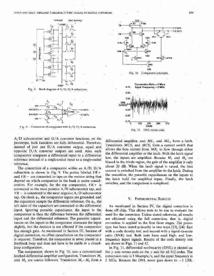
LEwIs AND CiRAY: PIPELINED 5-MsAkfpLE/s 9-BIT ANALOG-TO-DKHTALcONvERTER 959
S/H OUT DAC OUTPUT
y ;1 i8-VREF
Fig. 8. Block diagram of A/D, D\A subsection.
Fig. 9. Connection of comparator with A/D, D/A subsection.
A/D subconverter and D/A converter functions, on theprototype, both functions are fully differential. Therefore,instead of just one D/A converter output, equal andopposite D/A converter outputs are used. Also, eachcomparator compares a differential input to a differentialreference instead of a single-ended input to a single-endedreference.
The connection of a comparator within an A/D, D/Asubsection is shown in Fig. 9. The points labeled W? +and VR – are connected to taps on the resistor string thatdepend on which comparator in the bank is under consid-eration. For example, for the top comparator, VR + isconnected to the most positive A/D subconverter tap, andVR – is connected to the most negative A/D subconvertertap. On clock @l, the comparator inputs are grounded, andthe capacitors sample the differential reference. On @z,theleft sides of the capacitors are connected to the differentialinput. Ignoring parasitic capacitance, the ,input to thecomparator is then the difference between the differentialinput and the differential reference. The parasitic capaci-tances on the inputs to the comparator attenuate the inputslightly, but the decision is not affected if the comparatorhas enough gain. As mentioned in Section III, because ofdigital correction, no offset cancellation on the comparatoris required. Therefore, the comparator is never placed in afeedback loop and does not have to be stable in a closed-loop configuration.
The comparator, shown in Fig. 10, uses a conventionallatched-differential-amplifier configuration. Transistors Mland Mz are source followers. Transistors M3– Mg form a
4’ C OUT+
CB ~ ‘5 M6
VDD VDD ‘L1ML2
LT
C IN+; Ml M2 I C lN-
CSB+
‘B’”’ ; MS3
V;s
Fig. 10. Comparator schematic.
Conversion Rste. 5 Ms/s0.75
1Input Frequency ❑ 2 MHz
0.25
(L!!%)”.o
-0.25
-0.50
-o.750~12
Code
Fig. 11. DNL versus code.
differential amplifier, and ML1 and ML2 form a latch.Transistors MCS1 and MCS2 form a current switch thatallows the bias current from MB2 to flow through eitherthe differential amplifier or the latch. With the latch signallow, the inputs are amplified. Because M7 and M8 arebiased in the triode region, the gain of the amplifier is onlyabout 20 dB. When the latch signal is raised, the biascurrent is switched from the amplifier to the latch. Duringthe transition, the parasitic capacitances on the inputs tothe latch hold the amplified input. Finally, the latchswitches, and the comparison is completed.
V. EXPERIMENTAL RESULTS
As mentioned in Section IV, the digital correction isdone off chip. This allows tests to be run to evaluate theneed for the correction. Unless stated otherwise, all resultsare obtained using the full correction; that is, digitalcorrection is applied to the first three stages. The proto-type has been tested primarily in two ways [23], [24]: firstwith a code density test, and second with a signal-to-noiseratio (SNR) test. Both tests have used high- and low-frequency input signals. Results of the code density testare shown in Figs. 11 and 12.
In Fig. 11, differential nonlinearity (DNL) is plotted onthe y axis versus code on the x axis for all 512 codes. Theconversion rate is 5 Msample/s, and the input frequency is2 MHz. Because the DNL never goes down to – 1 LSB,

960 IEEEJOURNAL OF SOLID-STATECIRCUITS, VOL. SC-22, NO. 6, DECEMBER1987
Conversion Rate ❑ 5 MSIS1.25
1.00
0.75
0.50
0.25
(L!N~s) O.O-0.25-0.50-0.75-1.00
-1.250-512
Code
Fig. 12. INL versus code.
561 Conversion Rste = 5 Ms/s,
50!
SNR38(dB)32
201
1411.
-42 -36 -30 -24 -18 -12 -6 0Input Level (dB)
Fig, 13. SNR versus input level.
there are no missing codes. The maximum DNL is lessthan 0.6 LSB.
In Fig, 12, integral nonlinearity (INL) is plotted on they axis versus code on the x axis. Again, the conversion rateis 5 Msample/s and the input frequency is 2 MHz. Themaximum INL is 1.1 LSB. The nonideality in the curve iscaused by both nonlinearity in the first-stage D/A con-verter and incomplete settling of the first-stage op-ampoutput.
Under the same conditions as in Figs. 11 and 12 butwith the digital correction completely disabled, the maxi-mum DNL and INL are about 10 LSB at a 9-bit level,owing to comparator offsets. If the correction is appliedonly on the first stage, the maximum DNL and INL dropto about 3 LSB. When digital correction is applied on thefirst two stages, the maximum DNL is about 0.9 LSB andthe maximum INL is about 1.5 LSB; therefore, there areno missing codes in this case. Also, the uncorrected histo-gram data from the code density test show that there areno codes for which any residue is greater than the refer-ence level for comparator Cl or less than the referencelevel for comparator C’7as labeled in Fig. 8. This meansthat the maximum absolute value of nonlinearity in anA/D subconversion is less than or equal to 1/4 LSB at a3-bit level, and the full digital correction range (~ 1/2LSB) is not used. Therefore, comparators Cl and CT arenot needed in the last three stages.
SNR measurements were made by taking fast Fouriertransforms on 1024 samples from the A/D converter atthe downsampled rate of 20 kHz while the converter wasrunning at 5 Msample/s. In Fig. 13, SNR is plotted on they axis versus input level on the x axis for five input
TABLE IDATA SUMMARYOVERINPUT FREQUENCYVARIATION
9-bit Resolution; 5-Msample/s ConversionRate; ~ 5-V Power Supplies
frequencies: 2 kHz, 22 kHz, 202 kHz, 2.002 MHz, and5.002 MHz. The curve for 5.002 MHz represents a beatfrequency test on the converter when compared to thecurve for 2 kHz because the converter is running at thedifference between these two frequencies or 5 Msample/s.An ideal 9-bit curve is also shown. The peak SNR isaround 50 dB instead of 56 dB, as would be expected witha 9-bit converter; this difference is accounted for by distor-tion generated from the INL for large input signals. Whenthe input signal is reduced in amplitude, the distortion isreduced and the real curves approach the ideal 9-bit curve.Note that there is little difference in the curves for differ-ent input frequencies, showing that the first-stage S/Hamplifier is able to accurately sample high-frequency inputsignals.
The results of the code density and SNR tests forvariations in the input frequency are summarized in TableI. Peak DNL, INL, and SNR are shown for three inputfrequencies, and the performance is almost constant. Thisis important because it shows that the first-stage S/Hamplifier is able to accurately sample high-frequency inputsignals.
A photograph of the core of a prototype chip is shownin Fig. 14. The core is about 50 mil high by 150 rnil wide.The stages follow one after another and are identicalexcept that the fourth stage does not have a D/A con-verter or a subtracter and the two-phase nonoverlappingclock alternates from stage to stage. A test op amp and atest comparator are at the end. The prototype was madeby MOSIS in a 3-pm, double-polysilicon, p-well, CMOSprocess.
VI. SUMMARY
This paper reports on a prototype pipelined A/D con-verter with typical characteristics summarized in Table II.In summary, the prototype demonstrates that pipelinedarchitectures and digital correction techniques are ofpotential interest for high-speed CMOS A/D conversionapplications.
ACKNOWLEDGMENT
The authors gratefully acknowledge the help of R.Kavaler and J. Doernberg with the testing of the prototypeconverters.

LEWISAND GRAY: PIPELINED5-MSAMPLE\S9-BITANALOG-TO-DIGITALcONVERTER 961
[1]
[2]
[3]
[4]
[5]
[6]
[7]
[8]
[9]
[10]
[11]
Fig. 14. Photograph of the core of the prototype.
TABLE IITYPICAL PERFORMANCE:25°C
ITechnology 3-u CMOS
Resolution 9 bits
Conversion Rate 5 Msls
Area” 85(X3 mifs2
Power Supplies is v
Power Dissipation 180 mWInputCapaeiaurce 3 PFInputOffset <1 LSBCM InputRange k5 vDC PSRR 50dB
*Does not include clock gen-erator, bias generator, refer-ence generator, digital errorcorrection logic, and pads.
l@FERENCES
A. G. F. Dingwall, “Monolithic expandable 6 bit 20 MHzCMOS/SOS A/D converter; IEEE J. Solid-State Circuits, vol.SC-14, pp. 926-932, Dec. 1979.J. G, Peterson, “A monolithic video A/D converter,” IEEE J.Solid-State Circuits, vol. SC-14, pp. 932-937, Dec. 1979.T. Takemoto et al., “A fully parallel 10-blt A/D converter withvideo speed,” IEEE J. ,%lid-State Circuits, vol. SC-17, pp.1133-1138, Dec. 1982.Y. Fuiita et al.. “A bulk CMOS 20MSIS lb flash ADC.” in ISSCCDig. kech. Papers (San Francisco, CA), Feb. 1984, pp~ 56-57.A. G. F. Dingwall and V. Zazzu, ‘<High speed CMOS A/D andD/A conversion: in Dig. Tech. Papers, 1984 IEEE Int. Symp.Circuits Syst., May 1984, pp. 420-424.M. Inoue et al., “A monolithic 8-bit A/D converter with 120 MHzconversion rate; IEEE J, Solid-State Circuits, vol. SC-19, pp.837-841, Dec. 1984.T. Tsukada ef al., “CMOS 8b 25 MHz flash ADCfl in lSSCC Dig.Tech. Papers (New York, NY), Feb. 1985?pp. 34-35.A. K. Jov et a/.. “An inherently monotoruc 7-bit CMOS ADC forvideo ap~lication$” IEEE J. ;olid-State Circuits, vol. SC-21, pp.436–440. June 1986.T. Kumamoto et al., “An 8-bit high-speed CMOS A/D converter,”IEEE J. Solid-State Circuits, vol. SC-21, pp. 976-982, Dec. 1986.B. Peetz, B. D. Hamilton, and J. Kang, “An 8-bit 250 megasampleper second analog-to-digital converter: Operation without a sampleand hold,” IEEE. J. Solid-State Circuits, vol. SC-21, pp. 997–1002,Dec. 1986.Y. Yoshii et al., “An 8b 350MHz flash ADCj” in LSSCC Dig.Tech. Papers (New York, NY), Feb. 1987, pp. 96-97.
[12]
[13]
[14]
[15]
[16]
[17]
[18]
[19]
[20]
[21]
[22]
[23]
[24]
Y, Akazawa et al. “A 400MSPS 8b flash AD conversion LSIJ’ inJSSCC Dig. Tech. Papers (New York, NY), Feb. 1987, pp. 98-99.J. Corcoran et al., “A lGHz 6b ADC system,” in ZSSCC Dig.Tech. Papers (New York, NY) Feb. 1987, pp. 102-103.R. J. van de Plassche, “A high-speed 7 bit A/D converter,” IEEEJ. Solid-State Circuits, vol. SC-14, pp. 938-943, Dec. 1979.R. A. Blauschild. “An 8b 50ns monolikc A\D converter withinternal S/H,” in’ ISSCC Dig. Tech. Papers (N’ew York, NY) Feb.1983, pp. 178-179.R. E. J. van de Grift and R. J. van de Plassche, “A monolithic 8-bitvideo A/D converter,” IEEE J. Solid-State Circuits, vol. SC-19,pp. 374:378, June 1984.A. G. F. Dirmwall and V. Zazzu. “Au 8-MHz CMOS subranzirw8-bit A/D co&erter~ IEEE J. Solid-State Circuits, vol. SC-20,”pp~1138–1143, Dec. 1985.R. E. J. van de Grift and M. van der Veen, “An 8b 50 MHz ADCwith folding and interpolation techniques,” in LSSCC Dig. Tech.Papers (New York, NY), Feb. 1987, pp. 94-95.S. H. Lewis and P. R. Gray, “A pipelined 5MHz 9b ADCfl inISSCC Dig. Tech. Papers (New York, NY), Feb. 1987, pp. 210-211.0. A. Homa, “A 150 Mbps AID and D\A conversion system,”Comsat Tech .- Rev., vol. 2, no. 1, pp. 52-57, 1972.S. Taylor, “High speed analog-to-digital conversion in ;ntegratedcircuits,” Ph.D. dissertation, Univ. of Calif., Berkeley, pp. 30-42,1978R-.’Castello and P. R. Gray, “A high-performance micropowerswitched-capacitor filter,” IEEE J. Solid-State Circuits, vol. SC-20,pp. 1122–1132, Dec. 1985.W. A. Kester. “ Characterizirw and testin~ A/D and D/A con-verters for color video applic~tions,” IEEUE Trans. Circu;ts Syst.,vol. CAS-28, pp. 539–550, Jdy 1978.J, Doernberg, H. Lee, and D. A. Hodges, “Full-speed testing ofA \D converters.” IEEE J. Solid-State Circuits. vol. SC-19. DD.
8~0-827, Dec. 1984.. . .
Stephen H. Lewis received the B.S. degree fromRutgers University, New Brunswick, NJ, in 1979and the M.S. degree from Stanford University,Stanford, CA, in 1980.
From 1980 to 1982 he was with Bell Laborato-ries in Whippany, NJ, where he was involved incircuit design for magnetic recording. He is cnr-rently a student at the University of California,Berkeley, working toward the Ph.D. degree in thearea of integrated circuits.
Paul R. Gray (S’65-M69-SM’76-F’81), for photograph and biographyplease see this issue, p. 938.
Related Documents


