energies Article A New High-Gain DC-DC Converter with Continuous Input Current for DC Microgrid Applications Javed Ahmad 1 , Mohammad Zaid 2, *, Adil Sarwar 2 , Chang-Hua Lin 1 , Mohammed Asim 3 , Raj Kumar Yadav 4 , Mohd Tariq 2 , Kuntal Satpathi 5, * and Basem Alamri 6 Citation: Ahmad, J.; Zaid, M.; Sarwar, A.; Lin, C.-H.; Asim, M.; Yadav, R.K.; Tariq, M.; Satpathi, K.; Alamri, B. A New High-Gain DC-DC Converter with Continuous Input Current for DC Microgrid Applications. Energies 2021, 14, 2629. https://doi.org/10.3390/en14092629 Academic Editor: Teuvo Suntio Received: 18 March 2021 Accepted: 27 April 2021 Published: 4 May 2021 Publisher’s Note: MDPI stays neutral with regard to jurisdictional claims in published maps and institutional affil- iations. Copyright: © 2021 by the authors. Licensee MDPI, Basel, Switzerland. This article is an open access article distributed under the terms and conditions of the Creative Commons Attribution (CC BY) license (https:// creativecommons.org/licenses/by/ 4.0/). 1 Department of Electrical Engineering, National Taiwan University of Science and Technology, Taipei City 10607, Taiwan; [email protected] (J.A.); [email protected] (C.-H.L.) 2 Department of Electrical Engineering, ZHCET, Aligarh Muslim University, Aligarh 202002, India; [email protected] (A.S.); [email protected] (M.T.) 3 Electrical Engineering Department, Integral University, Lucknow 226021, India; [email protected] 4 Electronics Instrumentation & Control Engineering Department, College of Engineering, Ajmer 305001, India; [email protected] 5 Energy Exemplar (Singapore) Pte Ltd., 9 Battery Road, Singapore 049910, Singapore 6 Department of Electrical Engineering, College of Engineering, Taif University, Taif 21944, Saudi Arabia; [email protected] * Correspondence: [email protected] (M.Z.); [email protected] (K.S.) Abstract: The growth of renewable energy in the last two decades has led to the development of new power electronic converters. The DC microgrid can operate in standalone mode, or it can be grid-connected. A DC microgrid consists of various distributed generation (DG) units like solar PV arrays, fuel cells, ultracapacitors, and microturbines. The DC-DC converter plays an important role in boosting the output voltage in DC microgrids. DC-DC converters are needed to boost the output voltage so that a common voltage from different sources is available at the DC link. A conventional boost converter (CBC) suffers from the problem of limited voltage gain, and the stress across the switch is usually equal to the output voltage. The output from DG sources is low and requires high- gain boost converters to enhance the output voltage. In this paper, a new high-gain DC-DC converter with quadratic voltage gain and reduced voltage stress across switching devices was proposed. The proposed converter was an improvement over the CBC and quadratic boost converter (QBC). The converter utilized only two switched inductors, two capacitors, and two switches to achieve the gain. The converter was compared with other recently developed topologies in terms of stress, the number of passive components, and voltage stress across switching devices. The loss analysis also was done using the Piecewise Linear Electrical Circuit Simulation (PLCES). The experimental and theoretical analyses closely agreed with each other. Keywords: voltage stress; distributed generation (DG); high gain; quadratic boost 1. Introduction In recent years, the development of electricity-generation systems with nonconven- tional energy sources has called for a new generation of high-gain DC-DC converters [1]. High-gain converters can be nonisolated or isolated. Transformerless topologies are be- coming important in medium power applications up to 400–500 W due to their low cost and good efficiency. Conventional topologies of a DC-DC converter, like boost, SEPIC, and ZETA, have a simple structure, but their efficiency is low and for achieving high gain they need to be operated at high duty ratios, which leads to a substantial increase in the stress across the switching devices. Several topologies of high-gain DC-DC converters have been developed by researchers. Each of the configurations has its advantages and disadvantages. Usually, switched capacitors, voltage multiplier cells (VMCs), and switched inductors are used for increasing the gain. Common ground, isolation, and high efficiency are the key features that are available in isolated topologies [2] for high-power applications. High-gain Energies 2021, 14, 2629. https://doi.org/10.3390/en14092629 https://www.mdpi.com/journal/energies

Welcome message from author
This document is posted to help you gain knowledge. Please leave a comment to let me know what you think about it! Share it to your friends and learn new things together.
Transcript

energies
Article
A New High-Gain DC-DC Converter with Continuous InputCurrent for DC Microgrid Applications
Javed Ahmad 1 , Mohammad Zaid 2,*, Adil Sarwar 2 , Chang-Hua Lin 1 , Mohammed Asim 3,Raj Kumar Yadav 4, Mohd Tariq 2 , Kuntal Satpathi 5,* and Basem Alamri 6
Citation: Ahmad, J.; Zaid, M.;
Sarwar, A.; Lin, C.-H.; Asim, M.;
Yadav, R.K.; Tariq, M.; Satpathi, K.;
Alamri, B. A New High-Gain DC-DC
Converter with Continuous Input
Current for DC Microgrid
Applications. Energies 2021, 14, 2629.
https://doi.org/10.3390/en14092629
Academic Editor: Teuvo Suntio
Received: 18 March 2021
Accepted: 27 April 2021
Published: 4 May 2021
Publisher’s Note: MDPI stays neutral
with regard to jurisdictional claims in
published maps and institutional affil-
iations.
Copyright: © 2021 by the authors.
Licensee MDPI, Basel, Switzerland.
This article is an open access article
distributed under the terms and
conditions of the Creative Commons
Attribution (CC BY) license (https://
creativecommons.org/licenses/by/
4.0/).
1 Department of Electrical Engineering, National Taiwan University of Science and Technology,Taipei City 10607, Taiwan; [email protected] (J.A.); [email protected] (C.-H.L.)
2 Department of Electrical Engineering, ZHCET, Aligarh Muslim University, Aligarh 202002, India;[email protected] (A.S.); [email protected] (M.T.)
3 Electrical Engineering Department, Integral University, Lucknow 226021, India; [email protected] Electronics Instrumentation & Control Engineering Department, College of Engineering, Ajmer 305001, India;
[email protected] Energy Exemplar (Singapore) Pte Ltd., 9 Battery Road, Singapore 049910, Singapore6 Department of Electrical Engineering, College of Engineering, Taif University, Taif 21944, Saudi Arabia;
[email protected]* Correspondence: [email protected] (M.Z.); [email protected] (K.S.)
Abstract: The growth of renewable energy in the last two decades has led to the development ofnew power electronic converters. The DC microgrid can operate in standalone mode, or it can begrid-connected. A DC microgrid consists of various distributed generation (DG) units like solar PVarrays, fuel cells, ultracapacitors, and microturbines. The DC-DC converter plays an important rolein boosting the output voltage in DC microgrids. DC-DC converters are needed to boost the outputvoltage so that a common voltage from different sources is available at the DC link. A conventionalboost converter (CBC) suffers from the problem of limited voltage gain, and the stress across theswitch is usually equal to the output voltage. The output from DG sources is low and requires high-gain boost converters to enhance the output voltage. In this paper, a new high-gain DC-DC converterwith quadratic voltage gain and reduced voltage stress across switching devices was proposed. Theproposed converter was an improvement over the CBC and quadratic boost converter (QBC). Theconverter utilized only two switched inductors, two capacitors, and two switches to achieve the gain.The converter was compared with other recently developed topologies in terms of stress, the numberof passive components, and voltage stress across switching devices. The loss analysis also was doneusing the Piecewise Linear Electrical Circuit Simulation (PLCES). The experimental and theoreticalanalyses closely agreed with each other.
Keywords: voltage stress; distributed generation (DG); high gain; quadratic boost
1. Introduction
In recent years, the development of electricity-generation systems with nonconven-tional energy sources has called for a new generation of high-gain DC-DC converters [1].High-gain converters can be nonisolated or isolated. Transformerless topologies are be-coming important in medium power applications up to 400–500 W due to their low costand good efficiency. Conventional topologies of a DC-DC converter, like boost, SEPIC, andZETA, have a simple structure, but their efficiency is low and for achieving high gain theyneed to be operated at high duty ratios, which leads to a substantial increase in the stressacross the switching devices. Several topologies of high-gain DC-DC converters have beendeveloped by researchers. Each of the configurations has its advantages and disadvantages.Usually, switched capacitors, voltage multiplier cells (VMCs), and switched inductors areused for increasing the gain. Common ground, isolation, and high efficiency are the keyfeatures that are available in isolated topologies [2] for high-power applications. High-gain
Energies 2021, 14, 2629. https://doi.org/10.3390/en14092629 https://www.mdpi.com/journal/energies

Energies 2021, 14, 2629 2 of 14
non-isolated converters can also be used in microgrid applications with a bidirectionalpower flow [3]. In [4], a new non-isolated switched-capacitor based new boost converterwas proposed by the authors. The converter utilized two inductors and a single switch,but the gain was limited. The PV system mostly requires a step-up converter to enhancevoltage by utilizing the MPPT tracking function. In [5], a new improved boost converterfor renewable energy applications was proposed by the authors. In [6,7], a new high-gainboost and SEPIC converter with a continuous input current are proposed by the authors.Many techniques have been developed to enhance the gain with lower price and higherefficiency. A generalized structure of a high gain DC-DC converter with a single switchand switched inductors is proposed in [8]. The boost converter gain has been increasedby using the quadratic boost technique with high component voltage stress [9]. Despitethat, the output voltage was equal to the voltage stress. As a result, a higher rated switchwas used to compensate for the voltage stress on the provided switch, making excessiveconduction loss [10]. The quadratic boost converter can produce high voltage withoutextreme duty ratios. The conventional quadratic boost converter (CQBC) proposed in [11]had a single switch with a voltage stress equal to VO. In [12], a voltage doubler circuitwas introduced by the authors. With the help of diodes and switched capacitors, thevoltage at the output could be increased significantly. In [13], a new DC-DC Luo converterhaving positive output voltage was introduced. Only switched capacitors and diodeswere employed for increasing gain. Coupled inductor-based topologies are also popularto achieve very high gain. To achieve the desired gain, the coupled inductor’s turn ra-tio is adjusted, but this results in higher input current ripple. The high-gain convertersproposed in [14–17] addressed the problems associated with coupled inductor topologies.New boost converters with a voltage multiplier cell (VMC) were proposed by the authorsin [18–20]. VMC can be incorporated with conventional converters like boost, SEPIC, andconventional quadratic boost (CQBC) to increase the gain. A VMC employing switchedcapacitors suffers from the problem of high charging current, which results in additionalpower losses. Moreover, the number of components also increases when a VMC is used,leading to an increase in the cost and decrease in the reliability of the converter. Anotherfamily of converters are interleaved boost converters. These converters produce highgain at smaller duty ratios. An interleaved converter needs several VMCs [21–24] at theoutput to increase the voltage. In [25], a three-port DC-DC converter suitable for solar PVapplications was proposed by the authors. In [26], an extendable switched inductor basedhigh-gain converter was proposed by authors. The converter in [26] had continuous inputcurrent and reduced stress across switches, but many inductors were used to achieve highgain. In [27], a new hybrid switched-capacitor high-gain converter for DC microgrids wasproposed. In [28], a modified SEPIC converter was proposed for solar PV applications.In [29], a boost converter with a VMC was explained and discussed. However, the con-verter had many voltage-multiplier levels, but the converter still provided low voltage gain.A new high-gain converter with built-in transformers and a VMC was proposed in [30].In [31], a non-isolated high-gain converter with switched capacitors and voltage doublerswas proposed by the authors. In [32], a new QBC with a voltage doubler and a singleswitch was proposed by the authors. Some other recently developed high-gain convertershave been proposed by authors in [33–35]. Although these converters have high gain, thenumber of passive components is high. The main novelty of the converter proposed in thecurrent study is that it has a quadratic gain with only four passive elements. The otherfeatures of the converter are:
• Continuous input current;• Quadratic voltage gain with reduced voltage stress across switches;• High efficiency and easy control.
In subsequent sections, the workings of the proposed converter is discussed. Experi-mental results and efficiency of converter are reported in Sections 5 and 6. The conclusionsare discussed in Section 7.
Energies 2021, 14, 2629 3 of 14
2. Structure and Working of the Proposed Converter
The circuit diagram of the proposed converter is shown in Figure 1. The control signalis the same for both the switches. Based on the control signal, there are two modes ofoperation; that is, switch-on mode of operation and switch-off mode of operation. Themodes of operations can be explained as follows:
Energies 2021, 14, 2629 3 of 14
In subsequent sections, the workings of the proposed converter is discussed. Experimental
results and efficiency of converter are reported in Sections 5 and 6. The conclusions are
discussed in Section 7.
2. Structure and Working of the Proposed Converter
The circuit diagram of the proposed converter is shown in Figure 1. The control signal
is the same for both the switches. Based on the control signal, there are two modes of oper-
ation; that is, switch-on mode of operation and switch-off mode of operation. The modes of
operations can be explained as follows:
Vin S2 R
D2
VOC2
D1 L1
L2
S1 C1
+
+
+_
_VC1
VL1
VL2
+
_
-
Figure 1. The proposed converter.
Mode 1: Both the switches are turned ON simultaneously, and hence diodes D1 and
D2 are reverse-biased. The conduction diagram is given in Figure 2. In this operation
mode, both the capacitors discharge and transfer their energy to the inductors and to the
load, respectively, while both inductors store energy, and the inductor current subse-
quently increases linearly.
Vin R VOC2
L1
L2
C1
+
+
+_
_
_
VC1
VL1
VL2
+
_
Figure 2. Conduction diagram for the first mode of operation.
The governing equations for the first mode are as follows:
𝑉𝐿1 = 𝑉𝑖𝑛 + 𝑉𝐶1 (1)
𝑉𝐿2 = 𝑉𝑖𝑛 (2)
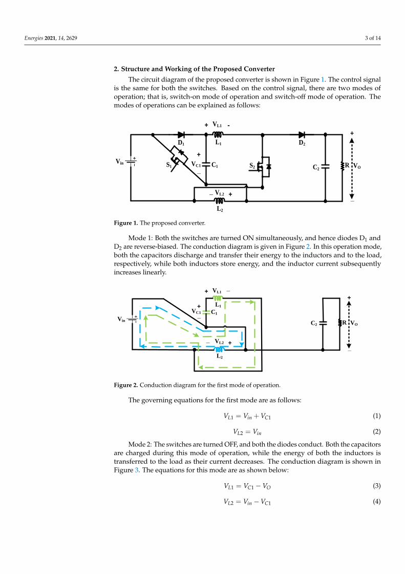
Mode 2: The switches are turned OFF, and both the diodes conduct. Both the capaci-
tors are charged during this mode of operation, while the energy of both the inductors is
transferred to the load as their current decreases. The conduction diagram is shown in
Figure 3. The equations for this mode are as shown below:
𝑉𝐿1 = 𝑉𝐶1 − 𝑉𝑂 (3)
Figure 1. The proposed converter.
Mode 1: Both the switches are turned ON simultaneously, and hence diodes D1 andD2 are reverse-biased. The conduction diagram is given in Figure 2. In this operation mode,both the capacitors discharge and transfer their energy to the inductors and to the load,respectively, while both inductors store energy, and the inductor current subsequentlyincreases linearly.
Energies 2021, 14, 2629 3 of 14
In subsequent sections, the workings of the proposed converter is discussed. Experimental
results and efficiency of converter are reported in Sections 5 and 6. The conclusions are
discussed in Section 7.
2. Structure and Working of the Proposed Converter
The circuit diagram of the proposed converter is shown in Figure 1. The control signal
is the same for both the switches. Based on the control signal, there are two modes of oper-
ation; that is, switch-on mode of operation and switch-off mode of operation. The modes of
operations can be explained as follows:
Vin S2 R
D2
VOC2
D1 L1
L2
S1 C1
+
+
+_
_VC1
VL1
VL2
+
_
-
Figure 1. The proposed converter.
Mode 1: Both the switches are turned ON simultaneously, and hence diodes D1 and
D2 are reverse-biased. The conduction diagram is given in Figure 2. In this operation
mode, both the capacitors discharge and transfer their energy to the inductors and to the
load, respectively, while both inductors store energy, and the inductor current subse-
quently increases linearly.
Vin R VOC2
L1
L2
C1
+
+
+_
_
_
VC1
VL1
VL2
+
_
Figure 2. Conduction diagram for the first mode of operation.
The governing equations for the first mode are as follows:
𝑉𝐿1 = 𝑉𝑖𝑛 + 𝑉𝐶1 (1)
𝑉𝐿2 = 𝑉𝑖𝑛 (2)
Mode 2: The switches are turned OFF, and both the diodes conduct. Both the capaci-
tors are charged during this mode of operation, while the energy of both the inductors is
transferred to the load as their current decreases. The conduction diagram is shown in
Figure 3. The equations for this mode are as shown below:
𝑉𝐿1 = 𝑉𝐶1 − 𝑉𝑂 (3)
Figure 2. Conduction diagram for the first mode of operation.
The governing equations for the first mode are as follows:
VL1 = Vin + VC1 (1)
VL2 = Vin (2)
Mode 2: The switches are turned OFF, and both the diodes conduct. Both the capacitorsare charged during this mode of operation, while the energy of both the inductors istransferred to the load as their current decreases. The conduction diagram is shown inFigure 3. The equations for this mode are as shown below:
VL1 = VC1 − VO (3)
VL2 = Vin − VC1 (4)
Energies 2021, 14, 2629 4 of 14
Energies 2021, 14, 2629 4 of 14
𝑉𝐿2 = 𝑉𝑖𝑛 − 𝑉𝐶1 (4)
VinR VOC2
L1
L2
C1
+
+
+_
_
_
VC1
VL1
VL2
+
_
Figure 3. Conduction diagram for the second mode of operation.
Applying the principle of volt-sec balance in inductor L2 and L1:
∫ 𝑉𝐿2(𝑡) · 𝑑𝑡 = 0𝑇
0
(5)
𝑉𝑖𝑛 × 𝐷𝑇 + (𝑉𝑖𝑛 − 𝑉𝐶1) × (1 − 𝐷)𝑇 = 0 (6)
𝑉𝐶1 =𝑉𝑖𝑛
1 − 𝐷 (7)
∫ 𝑉𝐿1(𝑡) · 𝑑𝑡 = 0𝑇
0
(8)
(𝑉𝑖𝑛 + 𝑉𝐶1) × 𝐷𝑇 + (𝑉𝐶1 − 𝑉𝑂) × (1 − 𝐷)𝑇 = 0 (9)
From Equations (7) and (9), the gain (M) is written as:
𝑀 =𝑉𝑜
𝑉𝑖𝑛=
(1 + 𝐷 − 𝐷2)
(1 − 𝐷)2 (10)
From Equation (10), it can be inferred that the voltage gain of the proposed converter
is quadratic.
3. Design of Passive Components and Stress across Switches
3.1. Design of Inductors
Rewriting the equation of the first mode of operation in a differential form, we get:
𝐿1
𝑑𝐼𝐿1
𝑑𝑡= 𝑉𝑖𝑛 + 𝑉𝐶1, 𝐿2
𝑑𝐼𝐿2
𝑑𝑡= 𝑉𝑖𝑛 (11)
Δ𝐼𝐿1 =(𝑉𝑖𝑛 + 𝑉𝐶1)𝐷𝑇
𝐿1, 𝛥𝐼𝐿2 =
𝑉𝑖𝑛𝐷𝑇
𝐿2 (12)
After combining Equations (7) and (12), we get:
Δ𝐼𝐿1 =𝑉𝑖𝑛(2 − 𝐷)𝐷𝑇
(1 − 𝐷)𝐿1 (13)
The average current through L1 and L2 are:
𝐼𝐿1 =𝑉𝑂
𝑅(1 − 𝐷), 𝐼𝐿2 =
𝑉𝑂(2𝐷 − 𝐷2)
𝑅(1 − 𝐷)2 (14)
Figure 3. Conduction diagram for the second mode of operation.
Applying the principle of volt-sec balance in inductor L2 and L1:∫ T
0VL2(t)·dt = 0 (5)
Vin × DT + (Vin − VC1)× (1 − D)T = 0 (6)
VC1 =Vin
1 − D(7)
∫ T
0VL1(t)· dt = 0 (8)
(Vin + VC1)× DT + (VC1 − VO)× (1 − D)T = 0 (9)
From Equations (7) and (9), the gain (M) is written as:
M =Vo
Vin=
(1 + D − D2)(1 − D)2 (10)
From Equation (10), it can be inferred that the voltage gain of the proposed converteris quadratic.
3. Design of Passive Components and Stress across Switches3.1. Design of Inductors
Rewriting the equation of the first mode of operation in a differential form, we get:
L1dIL1
dt= Vin + VC1, L2
dIL2
dt= Vin (11)
∆IL1 =(Vin + VC1)DT
L1, ∆IL2 =
VinDTL2
(12)
After combining Equations (7) and (12), we get:
∆IL1 =Vin(2 − D)DT(1 − D)L1
(13)
The average current through L1 and L2 are:
IL1 =VO
R(1 − D), IL2 =
VO(2D − D2)
R(1 − D)2 (14)
The minimum current through the inductors are as follows:
(IL1)Min =VO
R(1 − D)− Vin(2 − D)DT
2(1 − D)L1(15)

Energies 2021, 14, 2629 5 of 14
(IL2)Min =VO(2D − D2)
R(1 − D)2 − VinDTL2
(16)
For the continuous conduction operation mode, the minimum inductance requiredcan be calculated as given:
L1 ≥ (2 − D)D(1 − D)2Rfs(1 + D − D2)
(17)
L2 ≥ D(1 − D)4Rfs(1 + D − D2)
(18)
3.2. Design of Capacitor
The selection of a capacitor depends on the minimum permissible ripple in the voltageacross the capacitor. The charge stored by the capacitor is as follows:
∆Q = C∆VC (19)
IC∆T = C∆VC (20)
when the switch is ON, the current through each capacitor is as follows:
(IC1)ON =Vo
R(1 − D), (IC2)ON =
VoR
(21)
After combining (20), (21), and (10), the value of capacitors can be calculated as follows:
C1 =Vin(1 + D − D2)D
R(1 − D)3∆VC1 fs(22)
C2 =Vin(1 + D − D2)D
R(1 − D)2∆VC2 fs(23)
3.3. Voltage Stress across Switches
The voltage stress across the various components is given by (24) and (25). It can beseen from (24) and (25) that stress across the switch S1 and S2 is less than VO.
VS1 =Vin
1 − D=
VO(1 − D)
(1 + D − D2)(24)
VS2 =Vin
(1 − D)2 =VO
(1 + D − D2)(25)
The related waveforms during continuous conduction mode are shown in Figure 4.
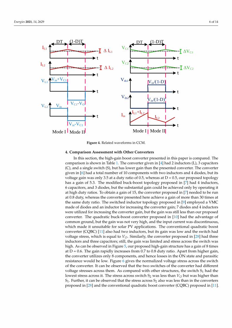
Energies 2021, 14, 2629 6 of 14Energies 2021, 14, 2629 6 of 14
IL2
IL1
VL1
VL2
DT (1-D)T
Mode I Mode II
t
t
t
t
Δ IL1
Δ IL2
VC1
VC2
Mode I Mode II
t
t
DT (1-D)T
Vin
Vin-VC1
VC1-VO
Vin+VC1
ΔVC1
ΔVC2
t
t
Vin/(1-D)
Vin/(1-D)2
Vds1
Vds2
Iin
t
IL1+IL2
IL2
Figure 4. Related waveforms in CCM.
4. Comparison Assessment with Other Converters
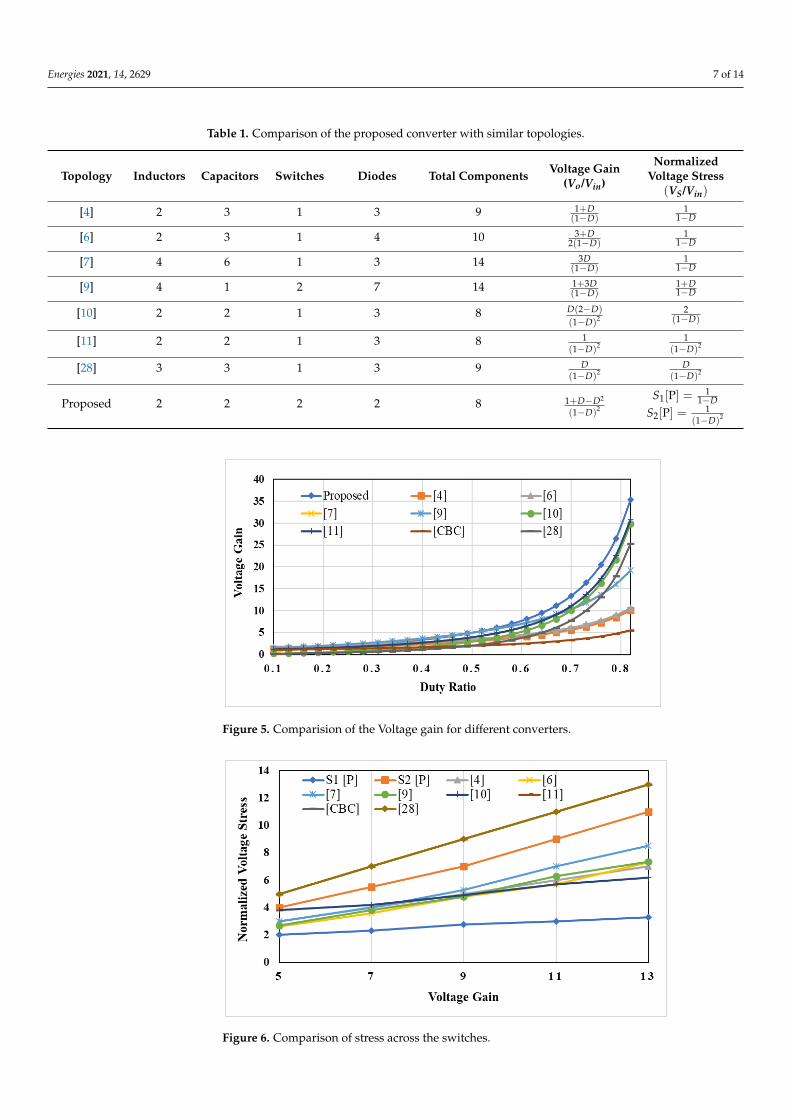
In this section, the high-gain boost converter presented in this paper is compared.
The comparison is shown in Table 1. The converter given in [4] had 2 inductors (L), 3
capacitors (C), and a single switch (S), but has lower gain than the presented converter.
The converter given in [6] had a total number of 10 components with two inductors and 4
diodes, but its voltage gain was only 3.5 at a duty ratio of 0.5, whereas at D = 0.5, our
proposed topology has a gain of 5.3. The modified buck-boost topology proposed in [7]
had 4 inductors, 6 capacitors, and 3 diodes, but the substantial gain could be achieved
only by operating it at high duty ratios. To obtain a gain of 15, the converter proposed in
[7] needed to be run at 0.8 duty, whereas the converter presented here achieve a gain of
more than 30 times at the same duty ratio. The switched inductor topology proposed in
[9] employed a VMC made of diodes and an inductor for increasing the converter gain; 7
diodes and 4 inductors were utilized for increasing the converter gain, but the gain was
still less than our proposed converter. The quadratic buck-boost converter proposed in
[10] had the advantage of common ground, but the gain was not very high, and the input
current was discontinuous, which made it unsuitable for solar PV applications. The con-
ventional quadratic boost converter (CQBC) [11] also had two inductors, but its gain was
low and the switch had voltage stress, which is equal to Vo. Similarly, the converter pro-
posed in [28] had three inductors and three capacitors; still, the gain was limited and stress
across the switch was high. As can be observed in Figure 5, our proposed high-gain struc-
ture has a gain of 8 times at D = 0.6. The gain rapidly increases from 0.7 to 0.8 duty ratio.
Apart from higher gain, the converter utilizes only 8 components, and hence losses in the
ON state and parasitic resistance would be low. Figure 6 gives the normalized voltage
stress across the switch of the converter. It can be observed that the two switches of the
converter had different voltage stresses across them. As compared with other structures,
the switch S1 had the lowest stress across it. The stress across switch S2 was less than Vo
but was higher than S1. Further, it can be observed that the stress across S2 also was less
than in the converters proposed in [28] and the conventional quadratic boost converter
(CQBC) proposed in [11].
Figure 4. Related waveforms in CCM.
4. Comparison Assessment with Other Converters
In this section, the high-gain boost converter presented in this paper is compared. Thecomparison is shown in Table 1. The converter given in [4] had 2 inductors (L), 3 capacitors(C), and a single switch (S), but has lower gain than the presented converter. The convertergiven in [6] had a total number of 10 components with two inductors and 4 diodes, but itsvoltage gain was only 3.5 at a duty ratio of 0.5, whereas at D = 0.5, our proposed topologyhas a gain of 5.3. The modified buck-boost topology proposed in [7] had 4 inductors,6 capacitors, and 3 diodes, but the substantial gain could be achieved only by operating itat high duty ratios. To obtain a gain of 15, the converter proposed in [7] needed to be runat 0.8 duty, whereas the converter presented here achieve a gain of more than 30 times atthe same duty ratio. The switched inductor topology proposed in [9] employed a VMCmade of diodes and an inductor for increasing the converter gain; 7 diodes and 4 inductorswere utilized for increasing the converter gain, but the gain was still less than our proposedconverter. The quadratic buck-boost converter proposed in [10] had the advantage ofcommon ground, but the gain was not very high, and the input current was discontinuous,which made it unsuitable for solar PV applications. The conventional quadratic boostconverter (CQBC) [11] also had two inductors, but its gain was low and the switch hadvoltage stress, which is equal to VO. Similarly, the converter proposed in [28] had threeinductors and three capacitors; still, the gain was limited and stress across the switch washigh. As can be observed in Figure 5, our proposed high-gain structure has a gain of 8 timesat D = 0.6. The gain rapidly increases from 0.7 to 0.8 duty ratio. Apart from higher gain,the converter utilizes only 8 components, and hence losses in the ON state and parasiticresistance would be low. Figure 6 gives the normalized voltage stress across the switchof the converter. It can be observed that the two switches of the converter had differentvoltage stresses across them. As compared with other structures, the switch S1 had thelowest stress across it. The stress across switch S2 was less than VO but was higher thanS1. Further, it can be observed that the stress across S2 also was less than in the convertersproposed in [28] and the conventional quadratic boost converter (CQBC) proposed in [11].
Energies 2021, 14, 2629 7 of 14
Table 1. Comparison of the proposed converter with similar topologies.
Topology Inductors Capacitors Switches Diodes Total Components Voltage Gain(Vo/Vin)
NormalizedVoltage Stress
(VS/Vin)
[4] 2 3 1 3 9 1+D(1−D)
11−D
[6] 2 3 1 4 10 3+D2(1−D)
11−D
[7] 4 6 1 3 14 3D(1−D)
11−D
[9] 4 1 2 7 14 1+3D(1−D)
1+D1−D
[10] 2 2 1 3 8 D(2−D)
(1−D)22
(1−D)
[11] 2 2 1 3 8 1(1−D)2
1(1−D)2
[28] 3 3 1 3 9 D(1−D)2
D(1−D)2
Proposed 2 2 2 2 8 1+D−D2
(1−D)2
S1[P] = 11−D
S2[P] = 1(1−D)2
Energies 2021, 14, 2629 7 of 14
Table 1. Comparison of the proposed converter with similar topologies.
Topology Inductors Capacitors Switches Diodes Total Components Voltage Gain
(𝑽𝒐 𝑽𝒊𝒏⁄ ) Normalized Voltage Stress
(𝑽𝑺 𝑽𝒊𝒏)⁄
[4] 2 3 1 3 9 1 + 𝐷
(1 − 𝐷)
1
1 − 𝐷
[6] 2 3 1 4 10 3 + 𝐷
2(1 − 𝐷)
1
1 − 𝐷
[7] 4 6 1 3 14 3𝐷
(1 − 𝐷)
1
1 − 𝐷
[9] 4 1 2 7 14 1 + 3𝐷
(1 − 𝐷)
1 + 𝐷
1 − 𝐷
[10] 2 2 1 3 8 𝐷(2 − 𝐷)
(1 − 𝐷)2
2
(1 − 𝐷)
[11] 2 2 1 3 8 1
(1 − 𝐷)2
1
(1 − 𝐷)2
[28] 3 3 1 3 9 𝐷
(1 − 𝐷)2
𝐷
(1 − 𝐷)2
Proposed 2 2 2 2 8 1 + 𝐷 − 𝐷2
(1 − 𝐷)2
𝑆1[P] =1
1 − 𝐷
𝑆2[P] =1
(1 − 𝐷)2
Figure 5. Comparision of the Voltage gain for different converters
Figure 6. Comparison of stress across the switches.
Figure 5. Comparision of the Voltage gain for different converters.
Energies 2021, 14, 2629 7 of 14
Table 1. Comparison of the proposed converter with similar topologies.
Topology Inductors Capacitors Switches Diodes Total Components Voltage Gain
(𝑽𝒐 𝑽𝒊𝒏⁄ ) Normalized Voltage Stress
(𝑽𝑺 𝑽𝒊𝒏)⁄
[4] 2 3 1 3 9 1 + 𝐷
(1 − 𝐷)
1
1 − 𝐷
[6] 2 3 1 4 10 3 + 𝐷
2(1 − 𝐷)
1
1 − 𝐷
[7] 4 6 1 3 14 3𝐷
(1 − 𝐷)
1
1 − 𝐷
[9] 4 1 2 7 14 1 + 3𝐷
(1 − 𝐷)
1 + 𝐷
1 − 𝐷
[10] 2 2 1 3 8 𝐷(2 − 𝐷)
(1 − 𝐷)2
2
(1 − 𝐷)
[11] 2 2 1 3 8 1
(1 − 𝐷)2
1
(1 − 𝐷)2
[28] 3 3 1 3 9 𝐷
(1 − 𝐷)2
𝐷
(1 − 𝐷)2
Proposed 2 2 2 2 8 1 + 𝐷 − 𝐷2
(1 − 𝐷)2
𝑆1[P] =1
1 − 𝐷
𝑆2[P] =1
(1 − 𝐷)2
Figure 5. Comparision of the Voltage gain for different converters
Figure 6. Comparison of stress across the switches.
Figure 6. Comparison of stress across the switches.

Energies 2021, 14, 2629 8 of 14
5. Experimental Results
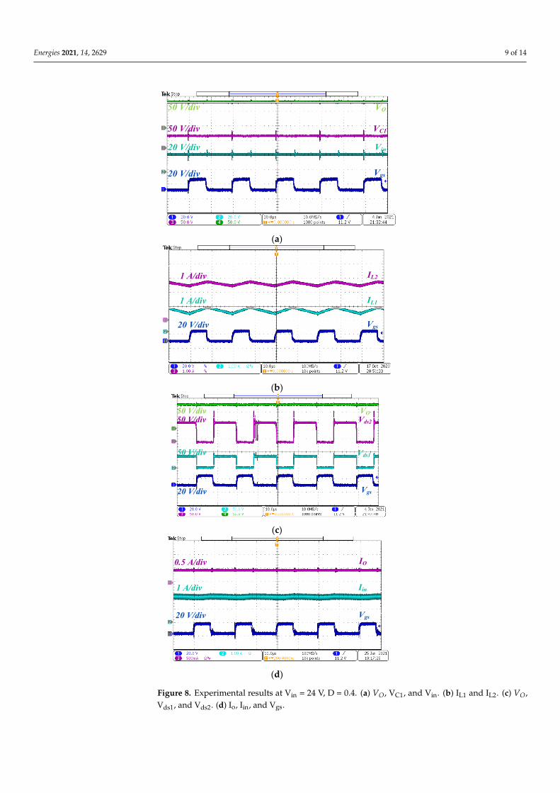
Table 2 shows the specifications of the presented converter. The simulation resultswere validated by running it on a hardware prototype. The working of the converter wastested by building a 150 W prototype as given in Figure 7. The prototype was operatedat a 0.4 duty ratio. From Figure 8a, the output voltage VO was equal to 80 V, which wasproximate to the theoretical value. The voltage across the capacitor was found to be 40 V,which was half the VO. The converter was operating in continuous conduction mode, asevident from the waveforms of the inductor currents shown in Figure 8b. The voltage stressacross switch S1 was found to be 40 V, and the stress across the switch S2 was found to be65 V, as observed in Figure 8c. The stress across both switches was less than VO, which wasan improvement over the other conventional topologies, thereby improving the efficiency.The converter had a continuous input current, which is its main advantage. The averageinput current Iin and output current IO were found to be 1.5 A and 0.4 A, respectively.Furthermore, the input current had a very low voltage ripple, which eliminated the needfor any input filter.
Table 2. Ratings of components.
Elements Rating/Model
Vin 24 V, 10 VPo (max) 150 W
fs 50 kHzR (Load) 250 Ω, 300 ΩInductors L1 = L2 = 330 µH, ESR = 0.2 ΩCapacitors C1 = C2 = 33 µF 200 V, ESR = 0.15 ΩS1 and S2 SPW52N50C3D1 and D2 SF8L60USM
Gate Drivers IC TLP250HMicrocontroller STM32 Nucleo H743ZI2
Energies 2021, 14, 2629 8 of 14
5. Experimental Results
Table 2 shows the specifications of the presented converter. The simulation results
were validated by running it on a hardware prototype. The working of the converter was
tested by building a 150 W prototype as given in Figure 7. The prototype was operated at
a 0.4 duty ratio. From Figure 8a, the output voltage Vo was equal to 80 V, which was prox-
imate to the theoretical value. The voltage across the capacitor was found to be 40 V, which
was half the Vo. The converter was operating in continuous conduction mode, as evident
from the waveforms of the inductor currents shown in Figure 8b. The voltage stress across
switch S1 was found to be 40 V, and the stress across the switch S2 was found to be 65 V,
as observed in Figure 8c. The stress across both switches was less than Vo, which was an
improvement over the other conventional topologies, thereby improving the efficiency.
The converter had a continuous input current, which is its main advantage. The average
input current Iin and output current IO were found to be 1.5 A and 0.4 A, respectively.
Furthermore, the input current had a very low voltage ripple, which eliminated the need
for any input filter.
Table 2. Ratings of components.
Elements Rating/Model
Vin 24 V, 10 V
Po (max) 150 W
fs 50 kHz
R (Load) 250 Ω, 300 Ω
Inductors L1 = L2 = 330 µH, ESR = 0.2 Ω
Capacitors C1 = C2 = 33 µF 200 V, ESR = 0.15 Ω
S1 and S2 SPW52N50C3
D1 and D2 SF8L60USM
Gate Drivers IC TLP250H
Microcontroller STM32 Nucleo H743ZI2
Figure 7. Prototype of the proposed converter. Figure 7. Prototype of the proposed converter.
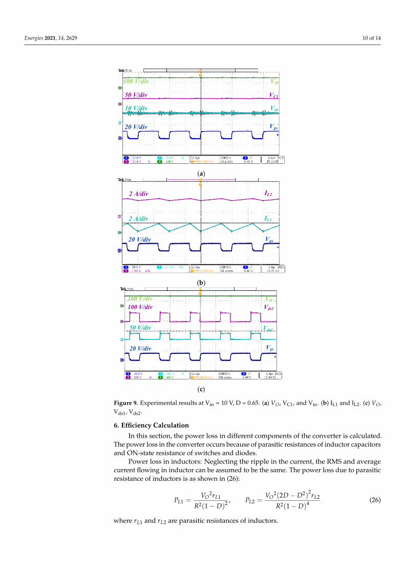
Figure 9a shows the experimental results at a duty ratio of 0.65 and input voltage of10 V, and it was found that the output voltage was almost 100 V, which also verified thecalculated gain of 10 times. The voltage across the capacitor C1 was 27 V, which was almostthe same as that of the calculated value. The inductor currents and voltage across switchesare shown in Figure 9b,c.
Energies 2021, 14, 2629 9 of 14Energies 2021, 14, 2629 9 of 14
Vgs20 V/div
Vin20 V/div
50 V/div
50 V/div
VC1
VO
(a)
Vgs20 V/div
IL21 A/div
IL11 A/div
(b)
Vgs20 V/div
Vds150 V/div
50 V/div50 V/div
Vds2
VO
(c)
Vgs20 V/div
IO0.5 A/div
Iin1 A/div
(d)
Figure 8. Experimental results at Vin = 24 V, D = 0.4. (a) Vo, VC1, and Vin. (b) IL1 and IL2. (c) Vo, Vds1, and Vds2. (d) Io, Iin, and Vgs.
Figure 9a shows the experimental results at a duty ratio of 0.65 and input voltage of 10 V, and it was found that the output voltage was almost 100 V, which also verified the
Figure 8. Experimental results at Vin = 24 V, D = 0.4. (a) VO, VC1, and Vin. (b) IL1 and IL2. (c) VO,Vds1, and Vds2. (d) Io, Iin, and Vgs.
Energies 2021, 14, 2629 10 of 14
Energies 2021, 14, 2629 10 of 14
calculated gain of 10 times. The voltage across the capacitor C1 was 27 V, which was almost the same as that of the calculated value. The inductor currents and voltage across switches are shown in Figure 9b,c.
Vgs20 V/div
Vin10 V/div
50 V/div
100 V/div
VC1
VO
(a)
Vgs20 V/div
IL22 A/div
IL12 A/div
(b)
Vgs20 V/div
Vds150 V/div
100 V/div100 V/div
Vds2
VO
(c)
Figure 9. Experimental results at Vin = 10 V, D = 0.65. (a) Vo, VC1, and Vin. (b) IL1 and IL2. (c) Vo, Vds1, Vds2.
6. Efficiency Calculation In this section, the power loss in different components of the converter is calculated.
The power loss in the converter occurs because of parasitic resistances of inductor capac-itors and ON-state resistance of switches and diodes.
Power loss in inductors: Neglecting the ripple in the current, the RMS and average current flowing in inductor can be assumed to be the same. The power loss due to parasitic resistance of inductors is as shown in (26):
Figure 9. Experimental results at Vin = 10 V, D = 0.65. (a) VO, VC1, and Vin. (b) IL1 and IL2. (c) VO,Vds1, Vds2.
6. Efficiency Calculation
In this section, the power loss in different components of the converter is calculated.The power loss in the converter occurs because of parasitic resistances of inductor capacitorsand ON-state resistance of switches and diodes.
Power loss in inductors: Neglecting the ripple in the current, the RMS and averagecurrent flowing in inductor can be assumed to be the same. The power loss due to parasiticresistance of inductors is as shown in (26):
PL1 =VO
2rL1
R2(1 − D)2 , PL2 =VO
2(2D − D2)2rL2
R2(1 − D)4 (26)
where rL1 and rL2 are parasitic resistances of inductors.

Energies 2021, 14, 2629 11 of 14
Power loss in capacitors: Similarly, the loss in capacitors due to ESR is as given below:
PC1 = i2C1RMSrC1
PC1 = VO2DrC1
R2(1−D)3
(27)
PC2 = i2C2RMSrC2
PC2 = VO2DrC2
R2(1−D)
(28)
Power loss in diodes: By knowing the RMS current, the average current of the totalpower loss across each diode is calculated as follows:
PD1 = VDiD1avg + i2D1RMSrD1
PD1 = VDVOR(1−D)
+ VO2rD
R2(1−D)4
(29)
PD1 = VDiD1avg + i2D1RMSrD1
PD2 = VDVOR(1−D)
+ VO2rD
R2(1−D)
(30)
where VD is the voltage drop across the diode.Power loss in the switch: There are two types of switch losses: conduction loss (PswCond)
and switching loss (Psw). These losses can be calculated as follows:
Psw = PswCond + PswON + PswOFF (31)
PswCond = I2swRMS rswON (32)
where rswON is ON-state resistance of MOSFET.
Psw1Cond =VO
2(2D − D2)2
R2(1 − D)4DrswON (33)
Psw2Cond =VO
2
R2(1 − D)2 rswON (34)
PswON =IswON VDD
2×
tri + t f v
2× fs (35)
Psw1ON =VO(2D − D2)Vin
2R(1 − D)3 ×tri + t f v
2× fs (36)
Psw2ON =VOVin
2R(1 − D)3 ×tri + t f v
2× fs (37)
Psw1OFF =VO(2D − D2)Vin
2R(1 − D)3 ×t f i + trv
2× fs (38)
Psw2OFF =VOVin
2R(1 − D)3 ×t f i + trv
2× fs (39)
where:tri+t f v
2 is turn ON time;t f i+trv
2 is turn OFF time; andfs is switching frequency.

Energies 2021, 14, 2629 12 of 14
To find the actual output voltage equation, we can combine all the losses and applythe law of conservation of power. A simplified output voltage equation considering onlyinductor and capacitor losses is provided in (40):
VO =
[Vin(1 − D)
(1 + D − D2)]R(1 − D)
R(1 − D)4 + rL1(1 − D)2 + rL2(4D2 + D2 − 4D3) + rC1D(1 − D) + rC2D(1 − D)3 (40)
Equation (40) can be verified by using the values of parameters from Table 2. Thevalue of VO is found to be 82.1 V for Vin = 24 V and D = 0.4, which is very close to theexperimental value of 80 V.
VO =
[24(1 − 0.4)
(1 + 0.4 − 0.42)](300)(1 − 0.4)
39 + 0.072 + 0.0272 + 0.036 + 0.013= 82.1 V (41)
The bifurcation of losses in converter is shown in Figure 10. The total losses in theMOSFETs accounted for 40% of the total losses. The total losses in diodes were 31%. InFigure 11, efficiency of converter is plotted at different values of input voltages. At lowinput voltages, the peak efficiency was found to be low. This is because high current flowsin the circuit for achieving the same output power, and hence more losses occurred in theconverter. The converter efficiency was high if the input voltages were between 24 and40 V. Usually, the output from the solar PV module is 24 V. Hence, the proposed convertermay be applied for stepping-up the voltage with high efficiency in the power range of200–300 W.
Energies 2021, 14, 2629 12 of 14
where:𝑡𝑟𝑖+𝑡𝑓𝑣
2 is turn ON time;
𝑡𝑓𝑖+𝑡𝑟𝑣
2 is turn OFF time; and
𝑓𝑠 is switching frequency.
To find the actual output voltage equation, we can combine all the losses and apply
the law of conservation of power. A simplified output voltage equation considering only
inductor and capacitor losses is provided in (40):
𝑉𝑂 =[𝑉𝑖𝑛(1 − 𝐷)(1 + 𝐷 − 𝐷2)]𝑅(1 − 𝐷)
𝑅(1 − 𝐷)4 + 𝑟𝐿1(1 − 𝐷)2 + 𝑟𝐿2(4𝐷2 + 𝐷2 − 4𝐷3) + 𝑟𝐶1𝐷(1 − 𝐷) + 𝑟𝐶2𝐷(1 − 𝐷)3 (40)
Equation (40) can be verified by using the values of parameters from Table 2. The
value of Vo is found to be 82.1 V for Vin = 24 V and D = 0.4, which is very close to the
experimental value of 80 V.
𝑉𝑂 =[24(1 − 0.4)(1 + 0.4 − 0.42)](300)(1 − 0.4)
39 + 0.072 + 0.0272 + 0.036 + 0.013= 82.1 𝑉 (41)
The bifurcation of losses in converter is shown in Figure 10. The total losses in the
MOSFETs accounted for 40% of the total losses. The total losses in diodes were 31%. In
Figure 11, efficiency of converter is plotted at different values of input voltages. At low
input voltages, the peak efficiency was found to be low. This is because high current flows
in the circuit for achieving the same output power, and hence more losses occurred in the
converter. The converter efficiency was high if the input voltages were between 24 and 40
V. Usually, the output from the solar PV module is 24 V. Hence, the proposed converter
may be applied for stepping-up the voltage with high efficiency in the power range of
200–300 W.
Figure 10. The breakup of losses of the proposed converter at 25 W output.
Figure 11. Efficiency of converter at different input voltages.
Figure 10. The breakup of losses of the proposed converter at 25 W output.
Energies 2021, 14, 2629 12 of 14
where:𝑡𝑟𝑖+𝑡𝑓𝑣
2 is turn ON time;
𝑡𝑓𝑖+𝑡𝑟𝑣
2 is turn OFF time; and
𝑓𝑠 is switching frequency.
To find the actual output voltage equation, we can combine all the losses and apply
the law of conservation of power. A simplified output voltage equation considering only
inductor and capacitor losses is provided in (40):
𝑉𝑂 =[𝑉𝑖𝑛(1 − 𝐷)(1 + 𝐷 − 𝐷2)]𝑅(1 − 𝐷)
𝑅(1 − 𝐷)4 + 𝑟𝐿1(1 − 𝐷)2 + 𝑟𝐿2(4𝐷2 + 𝐷2 − 4𝐷3) + 𝑟𝐶1𝐷(1 − 𝐷) + 𝑟𝐶2𝐷(1 − 𝐷)3 (40)
Equation (40) can be verified by using the values of parameters from Table 2. The
value of Vo is found to be 82.1 V for Vin = 24 V and D = 0.4, which is very close to the
experimental value of 80 V.
𝑉𝑂 =[24(1 − 0.4)(1 + 0.4 − 0.42)](300)(1 − 0.4)
39 + 0.072 + 0.0272 + 0.036 + 0.013= 82.1 𝑉 (41)
The bifurcation of losses in converter is shown in Figure 10. The total losses in the
MOSFETs accounted for 40% of the total losses. The total losses in diodes were 31%. In
Figure 11, efficiency of converter is plotted at different values of input voltages. At low
input voltages, the peak efficiency was found to be low. This is because high current flows
in the circuit for achieving the same output power, and hence more losses occurred in the
converter. The converter efficiency was high if the input voltages were between 24 and 40
V. Usually, the output from the solar PV module is 24 V. Hence, the proposed converter
may be applied for stepping-up the voltage with high efficiency in the power range of
200–300 W.
Figure 10. The breakup of losses of the proposed converter at 25 W output.
Figure 11. Efficiency of converter at different input voltages. Figure 11. Efficiency of converter at different input voltages.
Energies 2021, 14, 2629 13 of 14
7. Conclusions
A new high-gain converter was proposed and analyzed. The proposed converterutilized only a total of eight components to achieve high quadratic voltage gain. Usually,converters that produce quadratic voltage gain utilize more than three inductors andseveral diodes. The converter has a continuous input current, which is its main featureas it increases the life of solar PV panels. A hardware prototype of 150 W was developedin laboratory. Experimental results validated the workings and performance of converter.The converter was superior to quadratic boost, conventional boost, and other high-gainconverters in terms of gain and voltage stress across switch. The peak efficiency of theconverter was found to be 93.7% for Vin = 24 V. The merits of converter make it worthy forrenewable energy applications for an output power in the range of 200–300 W.
Author Contributions: All authors contributed equally in the preparation and revision of themanuscript. All authors have read and agreed to the published version of the manuscript.
Funding: The authors would like to acknowledge financial support from the Taif University Re-searchers Supporting Project (Number TURSP-2020/278), Taif University, Taif, Saudi Arabia. Theauthors also acknowledge the support provided by the Hardware-In-the-Loop (HIL) Lab and Non-Conventional Energy (NCE) Lab., Department of Electrical Engineering, Aligarh Muslim Univer-sity, India.
Institutional Review Board Statement: Not Applicable.
Informed Consent Statement: Not Applicable.
Data Availability Statement: Not Applicable.
Conflicts of Interest: The authors declare no conflict of interest.
References1. Forouzesh, M.; Siwakoti, Y.P.; Gorji, S.A.; Blaabjerg, F.; Lehman, B. Step-Up DC–DC Converters: A Comprehensive Review of
Voltage-Boosting Techniques, Topologies, and Applications. IEEE Trans. Power Electron. 2017, 32, 9143–9178. [CrossRef]2. Tofoli, F.L.; Pereira, D.D.C.; de Paula, W.J.; Júnior, D.D.S.O. Survey on non-isolated high-voltage step-up dc–dc topologies based
on the boost converter. IET Power Electron. 2015, 8, 2044–2057. [CrossRef]3. Cornea, O.; Andreescu, G.-D.; Muntean, N.; Hulea, D. Bidirectional Power Flow Control in a DC Microgrid Through a Switched-
Capacitor Cell Hybrid DC–DC Converter. IEEE Trans. Ind. Electron. 2017, 64, 3012–3022. [CrossRef]4. Shahir, F.M.; Babaei, E.; Farsadi, M. Voltage-Lift Technique Based Nonisolated Boost DC–DC Converter: Analysis and Design.
IEEE Trans. Power Electron. 2017, 33, 5917–5926. [CrossRef]5. Padmanaban, S.; Bhaskar, M.S.; Maroti, P.K.; Blaabjerg, F.; Fedák, V. An original transformer and switched capacitor (T &
SC)- based extension for DC-DC boost converter for high-voltage/low- current renewable energy applica-tions: Hardwareimplementation of a new T & SC boost converter. Energies 2018, 11, 783. [CrossRef]
6. Saravanan, S.; Babu, N.R. Design and Development of Single Switch High Step-Up DC–DC Converter. IEEE J. Emerg. Sel. Top.Power Electron. 2017, 6, 855–863. [CrossRef]
7. Banaei, M.R.; Sani, S.G. Analysis and Implementation of a New SEPIC-Based Single-Switch Buck–Boost DC–DC Converter WithContinuous Input Current. IEEE Trans. Power Electron. 2018, 33, 10317–10325. [CrossRef]
8. Shanthi, T.; Prabha, S.U.; Sundaramoorthy, K. Non-isolated n-stage High Step-up DC-DC Converter for Low voltage DC SourceIntegration. IEEE Trans. Energy Convers. 2021. [CrossRef]
9. Wu, B.; Li, S.; Liu, Y.; Smedley, K.M. A New Hybrid Boosting Converter for Renewable Energy Applications. IEEE Trans. PowerElectron. 2016, 31, 1203–1215. [CrossRef]
10. Gorji, S.A.; Mostaan, A.; My, H.T.; Ektesabi, M. Non-isolated buck–boost dc–dc converter with quadratic voltage gain ratio. IETPower Electron. 2019, 12, 1425–1433. [CrossRef]
11. Diaz-Saldierna, L.; Morales-Saldaña, J.; Ortiz-Lopez, M. Switching regulator using a quadratic boost converter for wide DCconversion ratios. IET Power Electron. 2009, 2, 605–613. [CrossRef]
12. Starzyk, J.A.; Jan, Y.-W.; Qiu, F. A DC-DC charge pump design based on voltage doublers. IEEE Trans. Circ. Syst. I Regul. Pap.2001, 48, 350–359. [CrossRef]
13. Luo, F.L.; Ye, H. Positive output multiple-lift push–pull switched capacitor Luo-converters. IEEE Trans. Ind. Electron. 2004, 51,594–602. [CrossRef]
14. Lee, S.-W.; Do, H.-L. Quadratic Boost DC–DC Converter With High Voltage Gain and Reduced Voltage Stresses. IEEE Trans.Power Electron. 2018, 34, 2397–2404. [CrossRef]

Energies 2021, 14, 2629 14 of 14
15. Wai, R.-J.; Lin, C.-Y.; Duan, R.-Y. High-efficiency DC-DC converter with high voltage gain and reduced switch stress. IEEE Trans.Ind. Electron. 2007, 54, 354–364. [CrossRef]
16. Lee, J.; Liang, T.; Chen, J. Isolated coupled-inductor-integrated DC-DC converter with non-dissipative snubber for solar energyapplications. IEEE Trans. Ind. Electron. 2014, 61, 3337–3348. [CrossRef]
17. Azizkandi, M.E.; Sedaghati, F.; Shayeghi, H.; Blaabjerg, F. A High Voltage Gain DC–DC Converter Based on Three WindingCoupled Inductor and Voltage Multiplier Cell. IEEE Trans. Power Electron. 2019, 35, 4558–4567. [CrossRef]
18. Duong, T.-D.; Nguyen, M.-K.; Tran, T.-T.; Lim, Y.-C.; Choi, J.-H. Transformerless High Step-Up DC-DC Converters with Switched-Capacitor Network. Electronics 2019, 8, 1420. [CrossRef]
19. Ahmad, J.; Zaid, M.; Sarwar, A.; Tariq, M.; Sarwer, Z. A New Transformerless Quadratic Boost Converter with High Voltage Gain.Smart Sci. 2020, 8, 1–21. [CrossRef]
20. Park, K.B.; Moon, G.W.; Youn, A.J. Non isolated high step-up boost converter integrated with sepic converter. IEEE Trans. PowerElectron. 2010, 25, 2266–2275. [CrossRef]
21. Meraj, M.; Bhaskar, M.S.; Iqbal, A.; Al-Emadi, N.; Rahman, S. Interleaved Multilevel Boost Converter With Minimal VoltageMultiplier Components for High-Voltage Step-Up Applications. IEEE Trans. Power Electron. 2020, 35, 12816–12833. [CrossRef]
22. Zhu, B.; Chen, S.; Zhang, Y.; Huang, Y. An Interleaved Zero-Voltage Zero-Current Switching High Step-Up DC-DC Converter.IEEE Access 2021, 9, 5563–5572. [CrossRef]
23. Alzahrani, A.; Ferdowsi, M.; Shamsi, P. A Family of Scalable Non-Isolated Interleaved DC-DC Boost Converters with VoltageMultiplier Cells. IEEE Access 2019, 7, 11707–11721. [CrossRef]
24. Dwari, S.; Parsa, L. An Efficient High-Step-Up Interleaved DC–DC Converter with a Common Active Clamp. IEEE Trans. PowerElectron. 2010, 26, 66–78. [CrossRef]
25. Deng, J.; Wang, H.; Shang, M. A ZVS Three-Port DC/DC Converter for High-Voltage Bus-Based Photovoltaic Systems. IEEETrans. Power Electron. 2019, 34, 10688–10699. [CrossRef]
26. Babaei, E.; Maheri, H.M.; Sabahi, M.; Hosseini, S.H. Extendable Non-isolated High Gain DC-DC Converter Based on Active–Passive Inductor Cells. IEEE Trans. Ind. Electron. 2018, 65, 9478–9487. [CrossRef]
27. Lakshmi, M.; Hemamalini, S. Non-isolated High Gain DC–DC Converter for DC Microgrids. IEEE Trans. Ind. Electron. 2018, 65,1205–1212. [CrossRef]
28. Iqbal, A.; Member, S. A New Structure of High Voltage Gain SEPIC Converter for Renewable Energy Applications. IEEE Access2019, 7, 89857–89868.
29. Rosas-Caro, C.J.; Mancilla-David, F.; Mayo-Maldonado, J.C.; Gonzalez-Lopez, J.M.; Torres-Espinosa, H.L.; Valdez-Resendiz, J.E. ATransformer-less High-Gain Boost Converter with Input Current Ripple Cancelation at a Selectable Duty Cycle. IEEE Trans. Ind.Electron. 2013, 60, 4492–4499. [CrossRef]
30. Guepfrih, M.F.; Waltrich, G.; Lazzarin, T.B. High Step-Up Dc-Dc Converter Using Built-in Transformer Voltage Multiplier Celland Dual Boost Concepts. IEEE J. Emerg. Sel. Top. Power Electron. 2021. [CrossRef]
31. Andrade, A.M.S.S.; Faistel, T.; Guisso, R.A.; Toebe, A. Hybrid High Voltage Gain Transformerless DC-DC Converter. IEEE Trans.Ind. Electron. 2021. [CrossRef]
32. Mahmood, A.; Zaid, M.; Ahmad, J.; Khan, M.A.; Khan, S.; Sifat, Z.; Lin, C.-H.; Sarwar, A.; Tariq, M.; Alamri, B. A Non-invertingHigh Gain DC-DC Converter with Continuous Input Current. IEEE Access 2021, 9, 54710–54721. [CrossRef]
33. Khan, S.; Mahmood, A.; Tariq, M.; Zaid, M.; Khan, I.; Rahman, S. Improved Dual Switch Non-Isolated High Gain Boost Converterfor DC microgrid Application. In Proceedings of the 2021 IEEE Texas Power and Energy Conference (TPEC), College Station, TX,USA, 2–5 February 2021; pp. 1–6. [CrossRef]
34. Khan, S.; Zaid, M.; Mahmood, A.; Ahmad, J.; Alam, A. A Single Switch High Gain DC-DC converter with Reduced Voltage Stress.In Proceedings of the 2020 IEEE 7th Uttar Pradesh Section International Conference on Electrical, Electronics and ComputerEngineering (UPCON), Prayagraj, India, 27–29 November 2020; pp. 1–6.
35. Zaid, M.; Ahmad, J.; Sarwar, A.; Sarwer, Z.; Tariq, M.; Alam, A. A Transformerless Quadratic Boost High Gain DC-DC Converter.In Proceedings of the 2020 IEEE International Conference on Power Electronics, Drives and Energy Systems (PEDES), Jaipur,India, 16–19 December 2020; pp. 1–6.
Related Documents