This article appeared in a journal published by Elsevier. The attached copy is furnished to the author for internal non-commercial research and education use, including for instruction at the authors institution and sharing with colleagues. Other uses, including reproduction and distribution, or selling or licensing copies, or posting to personal, institutional or third party websites are prohibited. In most cases authors are permitted to post their version of the article (e.g. in Word or Tex form) to their personal website or institutional repository. Authors requiring further information regarding Elsevier’s archiving and manuscript policies are encouraged to visit: http://www.elsevier.com/copyright

Welcome message from author
This document is posted to help you gain knowledge. Please leave a comment to let me know what you think about it! Share it to your friends and learn new things together.
Transcript

This article appeared in a journal published by Elsevier. The attachedcopy is furnished to the author for internal non-commercial researchand education use, including for instruction at the authors institution
and sharing with colleagues.
Other uses, including reproduction and distribution, or selling orlicensing copies, or posting to personal, institutional or third party
websites are prohibited.
In most cases authors are permitted to post their version of thearticle (e.g. in Word or Tex form) to their personal website orinstitutional repository. Authors requiring further information
regarding Elsevier’s archiving and manuscript policies areencouraged to visit:
http://www.elsevier.com/copyright

Author's personal copy
A microcontroller-based variable voltage variable frequency sinusoidalpower source with a novel PWM generation strategy
Pijus Kanti Sadhu, Gautam Sarkar ⇑, Anjan RakshitDepartment of Electrical Engineering, Jadavpur University, Kolkata, West Bengal 700 032, India
a r t i c l e i n f o
Article history:Received 22 April 2011Received in revised form 12 August 2011Accepted 26 September 2011Available online 12 October 2011
Keywords:Variable voltage variable frequency powersourceSinusoidal pulse width modulationMicrocontrollerMOSFET H-bridge inverterLCD display
a b s t r a c t
The present paper describes the development of a low cost, microcontroller-based variablevoltage variable frequency sinusoidal power source, which is the demand of the day forvarious applications. The power source is developed using MOSFET H-bridge inverterand with a stand alone LCD display system. The design methodology proposes to utilizea novel concept of generating sinusoidal pulse width modulation signals for the driver cir-cuit of the inverter. The system proposes to incorporate a ROM-based LUT within thepower source itself for the sinusoidal signal generation with enhanced stability. This lowcost, yet accurate power source has been successfully developed for wide range of voltagecommands (30–80 V rms) and frequency commands (40–70 Hz), and their real-life perfor-mances in voltage wave generation were also found to be quite satisfactory.
� 2011 Elsevier Ltd. All rights reserved.
1. Introduction
The efficient use of available power for various types ofdemand has remained an important issue in electricalengineering domain and hence has attracted attentionfrom many research communities all over the world. Thefocus has very often been to develop dedicated types ofpower sources according to specific, tailor-made demands.Very often, such requirements are specified in form of gen-eration of ac sources having variable magnitude, variablefrequency and different types of waveform shapes [1–5].Depending on requirement, there may be design anddevelopment of single phase [1,3] or three phase powersources [2,4,5]. Studies and analyses of suitable power con-verters in this regard have been going on for quite sometime [6–8]. Such power sources will be specifically usefulin characterization of performance of ac sources, e.g., inthree phase induction motor drive traction and also in tor-que and speed control, single phase induction motor forresidential applications. The quality of electrical power
developed is gradually becoming a matter of major con-cern as the new generation equipments installed forincreasing productivity very often turn out to be the majorsources of creating additional power quality problems.Hence, in an overall consideration, design of high quality,variable voltage variable frequency (VVVF) power sourcewith a wide range of peak-to-peak pure sine waveforms,with a wide range of frequency and with minimum distor-tion in the generated waveform, still remains a majorchallenge.
In [1], a DSP-based variable ac source was developedusing sliding mode control and Kalman filter methodology.This system achieved harmonic distortion of less than 2%in steady state response, while driving a linear, resistiveload. In [3], a microcontroller-based variable frequencypower inverter design was proposed for both single-phaseand three-phase systems. The microcontroller was used toprovide the pulse width modulation (PWM) signal for gatevoltage control drive of the IGBT inverter bridge. However,this system was only implemented in simulation. In [4], athree phase stable VVVF power source was developedusing a class D topology of power amplifiers and hysteresiscontrol strategy. In [5], a microcontroller-based threephase, three level voltage source inverter was developed
0263-2241/$ - see front matter � 2011 Elsevier Ltd. All rights reserved.doi:10.1016/j.measurement.2011.09.024
⇑ Corresponding author. Tel.: +91 9433088773; fax: +91 3324146184.E-mail address: [email protected] (G. Sarkar).
Measurement 45 (2012) 59–67
Contents lists available at SciVerse ScienceDirect
Measurement
journal homepage: www.elsevier .com/ locate/measurement
Author's personal copy
using two-level inverter topology. In recent times, effectiveinstantaneous frequency estimation schemes for a singlesinusoid [13,14] and for multiple sinusoids have also beenproposed. In [14], a scheme has been proposed for a porta-ble DSP-based instrumentation system where the fre-quency estimation is carried out on the basis of fourequal spaced samples. However, developments of such fre-quency estimators are known to be sensitive to deviationin sampling rate and quantization noise. In [15], an effec-tive scheme for estimation of quantized multiple sinusoidswas proposed using an iterative approach for optimizationof a nonlinear cost function. However, this efficient schemewas developed in simulation only, and no real-life imple-mentation was presented.
The present work describes the development of amicrocontroller-based single phase VVVF sinusoidal powersource employing MOSFET H-bridge inverter. The pro-posed scheme uses a novel concept of generating suitablePWM signals, called sinusoidal pulse width modulation(SPWM) technique, where constant amplitude pulses aregenerated with different duty cycles for each period. Thewidths of these pulses are suitably modulated to obtain in-verter output. The scheme is so designed that a read onlymemory (ROM)-based look-up table (LUT) is embeddedwithin the power source itself for the sinusoidal signalgeneration within the power source itself. This method of-fers several advantages such as improved stability andhigh-performance control over the generated sinusoidalsignal. The scheme uses two microcontrollers where onemicrocontroller is used to generate the proposed variablefrequency sine wave PWM drive and the other microcon-troller is used for controlling the stand alone LCD displayof the developed real power source. The developed schemehas been successfully employed for an ac voltage range of0–100 V rms and a frequency range of 40–70 Hz. The util-ity of the developed system is aptly demonstrated by cal-culating the desired performance in terms of totalharmonic distortion (THD) over a wide range of desiredcommands.
The rest of the manuscript is organized as follows.Section 2 describes the overall proposed VVVF power source.Section 3 details the power circuit design, Section 4 detailsthe control circuit and display circuit design, Section 5
details the driver circuit design, Section 6 details the powersupply circuit design and Section 7 details the protectioncircuit design. The performance evaluation is presented inSection 8. Conclusions are presented in Section 9.
Microcontroller-based VoltageController withFeed-forward
Compensation
Opto-isolatedVariable DC Source
230V50Hz
MOSFET H-bridge
VoltageControl
IsolationTransformer
FilterVariable Voltage
Variable FrequencyAC Output
High-side/Low-side Driver
Microcontroller-based PWM Drive
Microcontroller-based User Interface
FrequencyControl
LCD Display basedOutput Voltage andFrequency Monitor
StepdownTransformer and
Rectifier
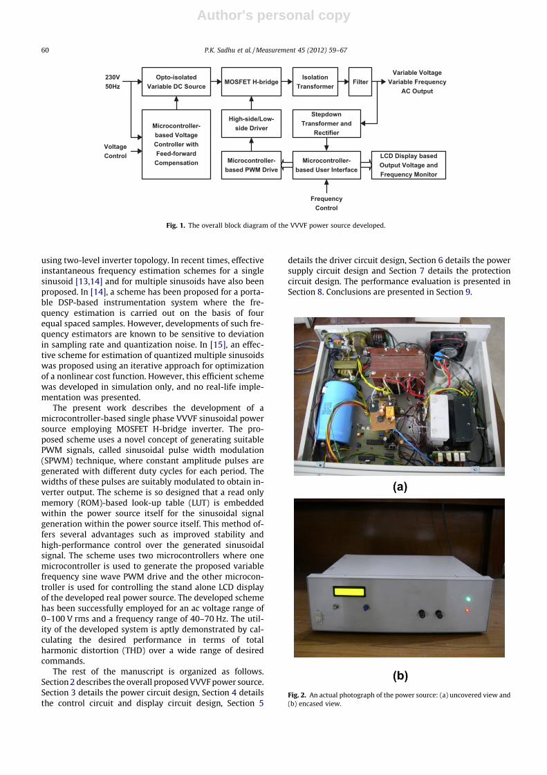
Fig. 1. The overall block diagram of the VVVF power source developed.
Fig. 2. An actual photograph of the power source: (a) uncovered view and(b) encased view.
60 P.K. Sadhu et al. / Measurement 45 (2012) 59–67
Author's personal copy
230V50Hz 9V
7805
++
+5V
+5V
PIC12F675
+9V unregulated
Voltagecontrol
To opto-isolatedvariable DC source
Signal for feed-forwardcompensation
Zero crossingdetector
P
N
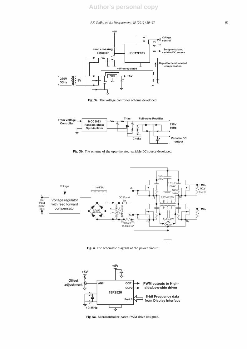
Fig. 3a. The voltage controller scheme developed.
MOC3023Random-phaseOpto-isolator
From VoltageController
Triac
230V50Hz
P
N
++
-
Variable DCoutput
Choke
Full-wave Rectifier
Fig. 3b. The scheme of the opto-isolated variable DC source developed.
In54084A/800V
Fig. 4. The schematic diagram of the power circuit.
18F2520
Offsetadjustment
+5V
10 MHz
+5V
8-bit Frequency datafrom Display InterfacePort B
CCP1 PWM outputs to High-side/Low-side driverCCP2
AN0
Fig. 5a. Microcontroller-based PWM drive designed.
P.K. Sadhu et al. / Measurement 45 (2012) 59–67 61
Author's personal copy
2. PIC microcontroller-based variable voltage variablefrequency (VVVF) power source
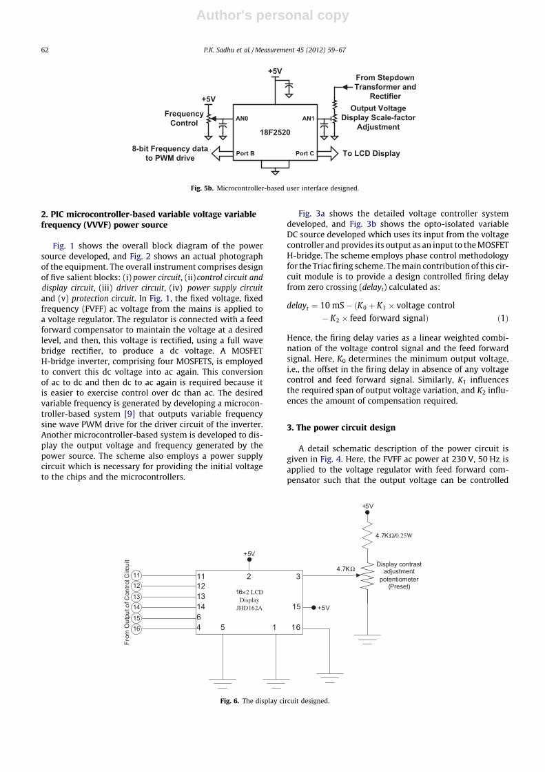
Fig. 1 shows the overall block diagram of the powersource developed, and Fig. 2 shows an actual photographof the equipment. The overall instrument comprises designof five salient blocks: (i) power circuit, (ii) control circuit anddisplay circuit, (iii) driver circuit, (iv) power supply circuitand (v) protection circuit. In Fig. 1, the fixed voltage, fixedfrequency (FVFF) ac voltage from the mains is applied toa voltage regulator. The regulator is connected with a feedforward compensator to maintain the voltage at a desiredlevel, and then, this voltage is rectified, using a full wavebridge rectifier, to produce a dc voltage. A MOSFETH-bridge inverter, comprising four MOSFETS, is employedto convert this dc voltage into ac again. This conversionof ac to dc and then dc to ac again is required because itis easier to exercise control over dc than ac. The desiredvariable frequency is generated by developing a microcon-troller-based system [9] that outputs variable frequencysine wave PWM drive for the driver circuit of the inverter.Another microcontroller-based system is developed to dis-play the output voltage and frequency generated by thepower source. The scheme also employs a power supplycircuit which is necessary for providing the initial voltageto the chips and the microcontrollers.
Fig. 3a shows the detailed voltage controller systemdeveloped, and Fig. 3b shows the opto-isolated variableDC source developed which uses its input from the voltagecontroller and provides its output as an input to the MOSFETH-bridge. The scheme employs phase control methodologyfor the Triac firing scheme. The main contribution of this cir-cuit module is to provide a design controlled firing delayfrom zero crossing (delayt) calculated as:
delayt ¼ 10 mS� ðK0 þ K1 � voltage control� K2 � feed forward signalÞ ð1Þ
Hence, the firing delay varies as a linear weighted combi-nation of the voltage control signal and the feed forwardsignal. Here, K0 determines the minimum output voltage,i.e., the offset in the firing delay in absence of any voltagecontrol and feed forward signal. Similarly, K1 influencesthe required span of output voltage variation, and K2 influ-ences the amount of compensation required.
3. The power circuit design
A detail schematic description of the power circuit isgiven in Fig. 4. Here, the FVFF ac power at 230 V, 50 Hz isapplied to the voltage regulator with feed forward com-pensator such that the output voltage can be controlled
18F2520
FrequencyControl
+5V
From StepdownTransformer and
Rectifier
+5V
8-bit Frequency datato PWM drive To LCD Display
Output VoltageDisplay Scale-factor
AdjustmentAN0 AN1
Port B Port C
Fig. 5b. Microcontroller-based user interface designed.
1112
11 2 3121314 1564 5 1 16
4.7K
+5V
+5V
+5V
16×2 LCD Display
JHD162A
4.7K /0.25W
Display contrast adjustment
potentiometer (Preset)
1314
1516
From
Out
puto
fCon
trolC
ircui
t
Fig. 6. The display circuit designed.
62 P.K. Sadhu et al. / Measurement 45 (2012) 59–67

Author's personal copy
at any desired level within the range 0–150 V, in steps of1 V, by a simple resistance potentiometer. The output fromthe regulator is applied to the full wave bridge rectifierthrough an inductor (i.e. a choke coil) to limit the currentduring switching. The rectifier performs the dc conversion,and at the output, a high value capacitor is connected toobtain a smooth, ripple free, dc output. A bleeder resis-tance is connected in parallel to provide a discharge pathfor the capacitor during off conditions.
The output from the rectifier is applied across a MOSFETH-bridge inverter, where four n-channel enhancementtype MOSFETs are connected in H shape. The switchingof these MOSFETs is controlled by the driver circuit. Thedriver circuit sends pulse to the gate and source of each
MOSFET. When the driver circuit sends pulse to a particu-lar MOSFET, it immediately turns ON, and when the pulseis withdrawn, the MOSFET is turned OFF. This sequence ofswitching is so designed that, at a particular switching in-stant, a pair of MOSFETs (say MOSFET1 and MOSFET4) is inON condition and the other pair (MOSFET2 and MOSFET3)is in OFF condition. In the next switching instant, just thereverse happens, i.e., MOSFET2 and MOSFET3 are turnedON and MOSFET1 and MOSFET4 are turned OFF. Here, eachMOSFET is protected by an R-C snubber circuit. The VVVFoutput from the power source is obtained by tapping theAC output from the MOSFET H-bridge inverter throughan isolation transformer, which is equipped with a filterbank in its secondary side.
IR2110
+5V
100µ
F/35
V
UF4007
UF4007
0.5
µF/3
0VD
isc10µF/
35V
UF4007
+12V
G1
S1
G2
S2
IR2110
+5V
100µ
F/35
V
UF4007
UF400710µF/35V
UF4007
+12V
G3
S3
G4
S4
10µF/35V
10µF/35V
Shut Down
10 /0.25W
10 /0.25W
0.1µ
F/30
VD
isc
0.1µ
F/30
VD
isc
18V/
1WZe
ner
18V/
1W
Zene
r
2N22
22
2N22
22
+5V
0.25W
0.25W
0.25W
FromProtection Circuit
0.5µ
F/30
VD
isc
0.5µ
F/30
VD
isc
0.5µ
F/30
VD
isc
From
Out
put o
f Con
trol C
ircui
t & D
ispl
ay C
ircui
t
1
2
3
4
0.25
0.25
Fig. 7. The driver circuit designed.
P.K. Sadhu et al. / Measurement 45 (2012) 59–67 63

Author's personal copy
4. The control circuit and display circuit design
This part of the circuit basically comprises a controlcircuit and a display circuit.
4.1. Control circuit
The design of the control circuit is achieved by usingtwo PIC18F2520 [10] microcontrollers: one, for managingthe analog frequency input and the display and the other,for production of the PWM pulse. Figs. 5a and 5b showthe two PIC 18F2520 microcontroller-based circuits indi-vidually, which are employed for microcontroller-basedPWM drive and microcontroller-based user interface de-sign and development, respectively. In the microcontrol-ler-based PWM drive module designed, CCP1 and CCP2are utilized to provide PWM outputs to high-side/low-sidedriver. Specifically, CCP1 generates the PWM firing signalwith 64 steps for the positive half cycle, and CCP2 gener-ates the PWM firing signal with 64 steps for the negative
half cycle. The novelty of this module designed lies inproviding an offset to the generation of a sinusoidal voltagestep value as a function of the PWM duty cycle look-uptable (LUT). This offset is instrumental in minimizing thetotal harmonic distortion (THD) of the sinusoidal outputdue to a finite ON/OFF time of MOSFET switching devicesfor a given PWM carrier frequency. A higher offset is re-quired for higher PWM carrier frequency for a given THDand vice versa. Hence, in this work, it is proposed to calcu-late the working PWM duty cycle (DPWM_W), for a givenstep, as:
DPWM W ¼ Offset þ ðDPWM � ðDPWM P � ð2� OffsetÞÞ=DPWM PÞð2Þ
where DPWM P is the peak duty cycle corresponding to thepeak of the sinusoidal voltage. This is selected as less than100% to cope with the problem of finite OFF-time of MOS-FET switching devices.
In the overall control circuit, the desired analog fre-quency is input by a resistance potentiometer, and this
Fig. 8. Schematic diagram of the power supply circuit designed.
Fig. 9. The protection circuit designed.
N2C.C.
Wattmeter
VavVrms
P.C.
A
N1
Lloyd-Fisher Magnetic Square
Variable Voltage Variable
Frequency Power Source
AC Supply 230V,50Hz
Fig. 10. Test setup for measurement of iron losses.
64 P.K. Sadhu et al. / Measurement 45 (2012) 59–67

Author's personal copy
information is converted to its digital form by using anADC, as shown in Fig. 5b. This digital frequency controlinformation is transmitted to the other microcontroller,shown in Fig. 5a, that produces the desired PWM pulseaccording to this digital frequency control, which is thentransmitted to the logic circuit. The microcontroller inFig. 5b, which is interfaced with the LCD display, receivesa feedback from the ac output of the power circuit, in a re-duced dc form (obtained using a step down transformerand a half wave rectifier), for display in the display circuit.
4.2. Display circuit
The display circuit comprises JHD162A, a 16 charac-ter � 2 row display chip [12]. Fig. 6 shows this circuit usedhere for display of output ac voltage and frequency.
5. The driver circuit design
The driver circuit designed is shown in detail in Fig. 7. Itis designed to receive input signal from the logic circuitand to produce suitable drives for the MOSFETs connectedin the H-bridge inverter. This driver circuit is designedutilizing the popular chip IR 2110 [11] which has the fol-lowing features:
(i) gate drive supply ranges from 10 V to 20 V,(ii) under voltage lockout for both channels,
(iii) matched propagation delay for both channels tosimplify use in high frequency applications,
(iv) the outputs produced are in phase with the inputs,(v) can drive independently high- and low-side refer-
enced output channels,
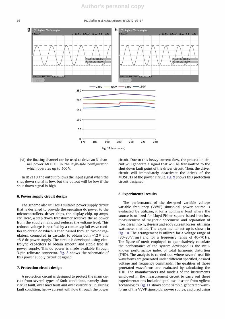
Fig. 11. DC output vs. line voltage variation for different voltage settings with feed forward compensation. (a) Captured waveform at 150 V (peak to peak)and 40 Hz, (b) captured waveform at 150 V (peak to peak) and 50 Hz, (c) captured waveform at 150 V (peak to peak) and 60 Hz, (d) captured waveform at150 V (peak to peak) and 70 Hz, (e) captured waveform at 200 V (peak to peak) and 40 Hz, (f) captured waveform at 200 V (peak to peak) and 50 Hz, (g)captured waveform at 200 V (peak to peak) and 60 Hz, (h) captured waveform at 200 V (peak to peak) and 70 Hz.
P.K. Sadhu et al. / Measurement 45 (2012) 59–67 65
Author's personal copy
(vi) the floating channel can be used to drive an N-chan-nel power MOSFET in the high-side configurationwhich operates up to 500 V.
In IR 2110, the output follows the input signal when theshut down signal is low, but the output will be low if theshut down signal is high.
6. Power supply circuit design
The scheme also utilizes a suitable power supply circuitthat is designed to provide the operating dc power to themicrocontrollers, driver chips, the display chip, op-amps,etc. Here, a step down transformer receives the ac powerfrom the supply mains and reduces the voltage level. Thisreduced voltage is rectified by a center tap full wave recti-fier to obtain dc which is then passed through two dc reg-ulators, connected in cascade, to obtain both +12 V and+5 V dc power supply. The circuit is developed using elec-trolytic capacitors to obtain smooth and ripple free dcpower supply. This dc power is made available through3-pin relimate connector. Fig. 8 shows the schematic ofthis power supply circuit designed.
7. Protection circuit design
A protection circuit is designed to protect the main cir-cuit from several types of fault conditions, namely shortcircuit fault, over load fault and over current fault. Duringfault condition, heavy current will flow through the power
circuit. Due to this heavy current flow, the protection cir-cuit will generate a signal that will be transmitted to theshut down fault point of the driver circuit. Then, the drivercircuit will immediately deactivate the drives of theMOSFETs of the power circuit. Fig. 9 shows this protectioncircuit designed.
8. Experimental results
The performance of the designed variable voltagevariable frequency (VVVF) sinusoidal power source isevaluated by utilizing it for a nonlinear load where thesource is utilized for Lloyd-Fisher square-based iron-lossmeasurement of magnetic specimens and separation ofiron losses into hysteresis and eddy current losses, utilizingwattmeter method. The experimental set up is shown inFig. 10. The arrangement is utilized for a voltage range of(30–80 V rms) and for a frequency range of 40–70 Hz.The figure of merit employed to quantitatively calculatethe performance of the system developed is the well-known performance index of total harmonic distortion(THD). The analysis is carried out where several real-lifewaveforms are generated under different specified, desiredvoltage and frequency commands. The qualities of thosegenerated waveforms are evaluated by calculating theTHD. The manufacturers and models of the instrumentsemployed in the measurement circuit to carry out theseexperimentations include digital oscilloscope from AgilentTechnologies. Fig. 11 shows some sample, generated wave-forms of the VVVF sinusoidal power source, captured using
Fig. 11 (continued)
66 P.K. Sadhu et al. / Measurement 45 (2012) 59–67

Author's personal copy
a digital storage oscilloscope. Table 1 shows the quantita-tive performance evaluation in some sample cases. Table 1and Fig. 11 in combination demonstrate that the proposedscheme can faithfully construct voltage waveforms overthe desired range of voltage and frequency commands.
Fig. 10 shows the utility of employing feed forwardcompensation in conjunction with the voltage controller.Here, the DC output voltage is plotted vs. line voltage var-iation for different voltage settings. This scheme is veryuseful in those situations where the line voltage does notremain steady at its nominal value (in our case, 230 V)and undergoes variation, usually in the lower side. Hadthere been no compensation provided, this curve wouldhave been a straight line passing through origin, with aslope of 45� with the horizontal axis. With incorporationof feed forward compensation, the scheme showed goodaccuracy in providing almost a straight line variation par-allel to the horizontal axis for different desired output DCvoltage settings (e.g. 160/180/200/220V DC).
9. Conclusion
A precision type, low cost, microcontroller-based vari-able voltage variable frequency sinusoidal power sourcehas been designed in this work. The developed schemehas been successfully employed for an ac voltage rangeof 30–80 V rms and a frequency range of 40–70 Hz. TheVVVF source has been developed employing MOSFETH-bridge inverter, and it introduces a novel concept ofgenerating suitable PWM signals, called sinusoidal pulsewidth modulation (SPWM) technique, where constantamplitude pulses are generated with different duty cyclesfor each period. Incorporation of a ROM-based LUT withinthe power source itself provides additional robustness anddesired performance achieving capability for the proposedscheme. The performance of the designed source has beensuccessfully demonstrated by its capability to faithfullyreproduce the commanded sine wave of desired amplitude
and frequency over their respective wide ranges. This pro-vides a simple, accurate, easy in operation power sourcewhich is a low cost solution compared to the standard,off-the-self products readily available in the market. Someof the commercially available products include those avail-able from Agilent� [16] (6811B AC Power Source/PowerAnalyzer), California Instruments [17] (251 TL), etc. How-ever, each such instrument is a high end equipment thatis highly expensive and may not be affordable for peoplein the research communities or in small industries, purelyfrom the economic point of view. One of the main objec-tives of the present work is to offer them a readymadesolution, at a much cheaper price. The scheme has beenpresently developed for generation of single phase ac volt-ages. The future scope of work will concentrate on devel-opment of similar power sources for generation of threephase voltages.
References
[1] K-S. Low, A DSP-based variable AC power source, IEEE Transaction onInstrumentation and Measurement 47 (4) (1998) 992–996.
[2] A. Cheritti, K. Al-Haddad, L. Dessaint, D. Mukhedkar, V. Rajagopalan,A variable frequency soft commutated voltage source inverterdelivering sinusoidal waveforms, industry applications societyannual meeting, in: Conference Record of the 1990 IEEE, vol. 1, pp.697–702.
[3] K.A. Madi-Ali, M.E. Salem Abozaed, Microcontroller based variablefrequency power inverter, in: Proc. International Multi Conference ofEngineers and Computer Scientists (IMECS), Hong Kong, March 17–19, 2010.
[4] F.R.S. Vincenzi et al., Programmable AC power source used to analyzeelectronic equipment performance in the electrical power systemquality concept, in: Twenty-third Annual IEEE Applied PowerElectronics Conference and Exposition, 2008, pp. 1931–1937.
[5] E. Mahrous, N.A. Rahim, W.P. Hew, Three phase three level voltagesource inverter with low switching frequency based on the two-levelinverter topology, IET Electrical Power Applications 1 (4) (2007)637–641.
[6] Ned Mohan, Tore M. Undeland, William P. Robins, Power Electronics:Converters, Applications, and Design, third ed., John Willy & Sons(Asia) Private Limited, 2002.
[7] R.W. Erickson, D. Maksimovic, Fundamentals of Power Electronics,second ed., Springer Science, 2001.
[8] M.H. Rashid, Power Electronics: Circuits, Devices and Applications,third ed., Prentice Hall of India Private Limited, 2003.
[9] A. Deshmukh, Microcontroller Theory and Applications, TataMcGraw-Hill Publishing Company Limited, New Delhi, 2007.
[10] Data Sheet of PIC 18F2520 Microcontroller from Microchip Inc.<http://www.microcontroller.com>.
[11] Data Sheet of IR 2110 from International Rectifier. <http://www.irf.com/product-info/datasheets/data/ir2110.pdf>.
[12] Data Sheet of LCD Display JHD162A. <http://www.electrokit.se/download/JHD162A%20SERIES.pdf>.
[13] D.N. Vizireanu, S.V. Halunga, Single sine wave parametersestimation method based on four equally spaced samples,International Journal of Electronics 98 (7) (2011) 941–948.
[14] D.N. Vizireanu, A simple and precise real-time four point singlesinusoid signals instantaneous frequency estimation method forportable DSP based instrumentation, Measurement 44 (2) (2011)500–502.
[15] R.M. Udrea, D.N. Vizireanu, Quantized multiple sinusoids signalestimation algorithm, Journal of Instrumentation (2008) 1–7.
[16] http://www.home.agilent.com/.[17] www.ProgrammablePower.com.
Table 1Sample THD evaluations for the power source designed.
Sl. no. RMS voltage output (V) Frequency (Hz) THD (%)
1 74.6 50.57 8.82 69.4 44.40 2.83 77.1 53.62 4.04 77.7 59.42 3.55 90.2 64.30 3.76 90.3 69.20 3.27 77.9 54.53 2.98 88.1 68.24 3.49 83.2 65.27 6.2
10 82.2 65.03 5.611 75.6 50.58 9.012 64.9 45.67 5.113 59.0 40.73 3.714 76.3 50.50 3.515 86.1 60.39 6.3
P.K. Sadhu et al. / Measurement 45 (2012) 59–67 67
Related Documents