Journal of the Mechanics and Physics of Solids 51 (2003) 47 – 67 www.elsevier.com/locate/jmps A methodology for determining mechanical properties of freestanding thin lms and MEMS materials H.D. Espinosa ∗ , B.C. Prorok, M. Fischer Department of Mechanical Engineering, Northwestern University, 2145 Sheridan Road, Evanston, IL 60208-3111, USA Received 16 October 2001; accepted 13 July 2002 Abstract We have developed a novel chip-level membrane deection experiment particularly suited for the investigation of sub-micron thin lms and microelectro-mechanical systems. The experiment consists of loading a xed–xed membrane with a line load applied at the middle of the span using a nanoindenter. A Mirau microscope interferometer is positioned below the membrane to observe its response in real time. This is accomplished through a micromachined wafer con- taining a window that exposes the bottom surface of the specimen. A combined atomic force microscope/nanoindenter incorporates the interferometer to allow continuous monitoring of the membrane deection during both loading and unloading. As the nanoindenter engages and de- ects the sample downward, fringes are formed and acquired by means of a CCD camera. Digital monochromatic images are obtained and stored at periodic intervals of time to map the strain eld. Stresses and strains are computed independently without recourse to mathematical assumptions or numerical calibrations. Additionally, no restrictions on the material behavior are imposed in the interpretation of the data. In fact, inelastic mechanisms including strain gradient plasticity, piezo and shape memory eects can be characterized by this technique. The test methodology, data acquisition and reduction are illustrated by investigating the re- sponse of 1-m thick gold membranes. A Young’s modulus of 53 GPa, a yield stress of 55 MPa and a residual stress of 12 MPa are consistently measured. The post-yield behavior leading to fracture exhibits typical statistical variations associated to plasticity and microcrack initiation. ? 2002 Elsevier Science Ltd. All rights reserved. Keywords: Thin lms; MEMS materials; Micro-tensile test; Mechanical properties ∗ Corresponding author. Tel.: +1-847-4675989; fax: +1-847-4913540. E-mail address: [email protected] (H.D. Espinosa). URL: http://clifton.mech.nwu.edu/∼espinosa 0022-5096/02/$ - see front matter ? 2002 Elsevier Science Ltd. All rights reserved. PII: S0022-5096(02)00062-5

Welcome message from author
This document is posted to help you gain knowledge. Please leave a comment to let me know what you think about it! Share it to your friends and learn new things together.
Transcript

Journal of the Mechanics and Physics of Solids51 (2003) 47–67
www.elsevier.com/locate/jmps
A methodology for determining mechanicalproperties of freestanding thin (lms and MEMS
materialsH.D. Espinosa∗, B.C. Prorok, M. Fischer
Department of Mechanical Engineering, Northwestern University, 2145 Sheridan Road, Evanston,IL 60208-3111, USA
Received 16 October 2001; accepted 13 July 2002
Abstract
We have developed a novel chip-level membrane de7ection experiment particularly suited forthe investigation of sub-micron thin (lms and microelectro-mechanical systems. The experimentconsists of loading a (xed–(xed membrane with a line load applied at the middle of the spanusing a nanoindenter. A Mirau microscope interferometer is positioned below the membrane toobserve its response in real time. This is accomplished through a micromachined wafer con-taining a window that exposes the bottom surface of the specimen. A combined atomic forcemicroscope/nanoindenter incorporates the interferometer to allow continuous monitoring of themembrane de7ection during both loading and unloading. As the nanoindenter engages and de-7ects the sample downward, fringes are formed and acquired by means of a CCD camera.Digital monochromatic images are obtained and stored at periodic intervals of time to map thestrain (eld. Stresses and strains are computed independently without recourse to mathematicalassumptions or numerical calibrations. Additionally, no restrictions on the material behavior areimposed in the interpretation of the data. In fact, inelastic mechanisms including strain gradientplasticity, piezo and shape memory e=ects can be characterized by this technique.
The test methodology, data acquisition and reduction are illustrated by investigating the re-sponse of 1-�m thick gold membranes. A Young’s modulus of 53 GPa, a yield stress of 55 MPaand a residual stress of 12 MPa are consistently measured. The post-yield behavior leading tofracture exhibits typical statistical variations associated to plasticity and microcrack initiation.? 2002 Elsevier Science Ltd. All rights reserved.
Keywords: Thin (lms; MEMS materials; Micro-tensile test; Mechanical properties
∗ Corresponding author. Tel.: +1-847-4675989; fax: +1-847-4913540.E-mail address: [email protected] (H.D. Espinosa).URL: http://clifton.mech.nwu.edu/∼espinosa
0022-5096/02/$ - see front matter ? 2002 Elsevier Science Ltd. All rights reserved.PII: S0 0 2 2 -5 0 9 6 (02)00062 -5

48 H.D. Espinosa et al. / J. Mech. Phys. Solids 51 (2003) 47–67
1. Introduction
Thin (lms are customarily employed in microelectronic components and microelectro-mechanical systems (MEMS) devices. Their properties frequently allow essential devicefunctions and therefore accurate identi(cation of these properties is key to the develop-ment of new technologies. In some applications, the demands placed on thin (lms cansometimes subject them to various mechanical conditions leading to fracture, plasti-city, friction and wear, creep, fatigue, etc. Unfortunately, most of our knowledge inthese areas is based on bulk material behavior, which many times fails to describematerial response in this size regime. This is the case due primarily to surface andinterface e=ects, limited number of grains in a given volume, and the role played bythe manufacturing process. This last feature is very important in view that specimensurfaces are the result of the process employed to remove material. For instance, dryand wet etching lead to di=erences in surface roughness. Likewise, di=erent chemicalsutilized as etchings as well as process parameters, such as temperature and time, con-tribute to produce surfaces with well-de(ned features and defects, e.g., striations. Manyresearchers are currently investigating the mechanical response of thin (lms, e.g., Yuanand Sharpe (1997), Vlassak and Nix (1992), Chasiotis and Knauss (1998), Drory andHutchinson (1995), Evans et al. (1997), and Huang and Spaepen (1996). Frequently,each particular investigation involving MEMS tends to be device dependent and intro-duces new fundamental questions. Progress in this (eld has leaned towards providingmore speci(c technological solutions rather than generating a basic understanding ofmechanical behavior.
Techniques to study MEMS materials’ response to mechanical loading are diverseand can be classi(ed as static or dynamic. Although both will yield the materials’mechanical properties, they accomplish it in completely di=erent manners. Within thestatic group are nanoindentation (in standard DC mode), (Nix, 1989, Oliver and Pharr,1992), micro-tensile (Yuan and Sharpe, 1997) bending (Sharpe, 1995, 1996; Zeng andSharpe, 1996) and bulge tests (Small and Nix, 1992; Vlassak and Nix, 1992; Smallet al., 1994). Nanoindentation, when the continuous sti=ness measurement feature isused, resonance and fatigue methods (Kiesewetter et al., 1992; Osterberg and Senturia,1997; Manceau et al., 1996) belong to the dynamic group.
Conventional understanding of material yielding and fracture does not apply at thisscale because of the increased role that interface-driven processes play. Thus, there isa need to establish novel testing methodologies that measure stress and strain directlyand independently on a variety of specimen geometries. The equivalent of a tensiletest customary performed on bulk samples is desirable in this regard. Loads and strainsare measured directly and independently, and no mathematical assumptions are neededto identify quantities describing the material response. Techniques that use a special(xture to load small tensile samples have been developed (Sharpe, 1995, 1996; Zengand Sharpe, 1996; Chasiotis and Knauss, 1998). These techniques employ a dog-bonetype specimen that is (xed at one end and freestanding at the other end. A probe isattached to the freestanding end to elongate/load the specimen. Sophisticated proceduresfor attaching the probes, by employing electrostatic forces or UV curing glues, weredeveloped by Sharpe at Johns Hopkins University and W. Knauss at Caltech. However,

H.D. Espinosa et al. / J. Mech. Phys. Solids 51 (2003) 47–67 49
stress–strain curves cannot be uniquely determined when the various techniques arecompared (Sharpe et al., 1998). This is due in part to microfabrication steps, such aschemical etching, which a=ect the specimens and tests’ outcome in di=erent manners.Note that specimens employed in di=erent testing techniques have not only di=erencesin geometry but also in microfabrication steps.
An ideal architecture to achieve a direct tensile testing scheme involves a freestandingmembrane (xed at both ends. A line load applied at the middle of the span producesa uniform stretch on the two halves of the thin membrane. We have demonstrated thistesting scheme by the investigation of radio frequency (RF) MEMS switches, producedby Raytheon Systems Co. (Fischer, 1999; Espinosa et al., 2001a–c). In this method wemade use of a nanoindenter to apply a line load at the center of the membrane. Pushingthe membrane down tests the specimen structural response and provides informationon its elastic behavior and residual stress state. In this manner, simple tension of themembrane is achieved except for boundary bending e=ects.
A critical concern in this membrane de7ection experiment (MDE) was accountingfor the thermal drift and spring constant of the nanoindenter column. Since the columndimension is orders of magnitude larger than the membrane de7ection, minute changesin temperature, a fraction of a degree C, can signi(cantly a=ect displacement measure-ments. To account for these two factors, we made indents on either post supporting themembrane. Corrections for thermal drift and spring constant were then calculated fromthe approach segment data before contact with the posts. Other important information isalso gained from these indents such as; device tilt, height of the membrane at contact,and middle position in the plane of the (lm. The load-displacement data can then beadjusted accordingly. We use a similar testing methodology here to examine elasticity,plasticity and fracture of thin (lms although the specimen geometry and wafer aremodi(ed to achieve homogeneous deformations.
The paper is organized as follows. The specimen design and microfabrication proce-dure are (rst discussed. Details on testing methodology and setup are then given withparticular attention to features that a=ect the measurements accuracy. The algorithmfor data reduction, accounting for the optical path of the interferometer light and mem-brane geometry, is presented and followed by discussion of experimentally obtainedstress–strain curves in gold (lms. Test repeatability and size e=ects on elasticity, plas-ticity and fracture are addressed to illustrate the potential of the developed chip-levelexperiment.
2. Membrane de�ection experiment (MDE)
2.1. Specimen design
The specimen geometry utilized in this study resembles the typical dog-bone tensilespecimen but with an area of additional width in the center designed as the contactarea where the line load is applied, Fig. 1. This measure is taken to minimize stressconcentrations where the loading device contacts the membrane. The suspended mem-branes are (xed to the wafer at either end such that they span the bottom view window.

50 H.D. Espinosa et al. / J. Mech. Phys. Solids 51 (2003) 47–67
Fig. 1. Optical image of three Au membranes showing characteristic dimensions. LM is half the membranespan, and W is the membrane width.
In the areas where the membrane is attached to the wafer and in the central contactarea, the width is varied in such a fashion to minimize boundary-bending e=ects. Thesee=ects are also minimized through large specimen gauge lengths. Thus, a load appliedin the center of the span results in direct stretching of the membrane in the areas ofthin constant width in the same manner as in a direct tension test.
Several types and sizes of membrane specimens were designed on a single wafer.Fig. 2 is a schematic drawing indicating particulars of the membrane dimensions. Actualvalues are listed in Table 1. The di=erent types and sizes of membranes are representedin individual windows of each die, 68 dies per 4 in wafer, where membranes are placed5 per window, Fig. 3. In this study we will report on only two di=erent sized tensilespecimens as a proof of concept for this methodology, tensile specimens “d” and “e”.These two specimens possess identical shape, but at di=erent length scales.
2.2. Micro fabrication of specimens
The suspended membrane specimens were fabricated on (1 0 0) Si wafers with doublesided polishing. Fig. 4 is a schematic drawing summarizing the microfabrication steps.A layer of Si3N4 was deposited in both sides of the wafer to act as etch stops toaid in de(ning the bottom view windows and to protect the membranes during wetetching of Si. Windows were then dry etched into the Si3N4 on the bottom side.

H.D. Espinosa et al. / J. Mech. Phys. Solids 51 (2003) 47–67 51
Fig. 2. Schematic of membrane geometry indicating the di=erent parameters used to de(ne specimen dimen-sions.
Table 1Membrane dimensions for di=erent sized specimens
Dimensions (�m) Sample type
Tensile specimens Fracture specimens
A B C D E F G H
±2 514 362 286 1425 818 514 818 1425E ±0:5 45 22.5 11.25 180 90 45 90 180L ±0:5 100 50 25 400 200 100 200 400W ±0:1 5 2.5 1.25 20 10 10 20 40M ±0:5 10 10 10 10 10 10 10 10N ±1 100 100 100 100 100 100 100 100R ±0:5 20 10 5 80 40 20 40 80S ±0:5 17.32 8.66 4.33 69.28 34.64 17.32 34.64 69.28H ±0:1 — — — — — 1 2 4.5
±0:1 — — — — — 1 1 1LW ±2 2078.5 2078.5 2078.5 2078.5 2078.5 2078.5 2078.5 2078.5WW ±2 1112.7 960.8 884.8 2024.5 1416.7 1112.7 1416.7 2024.5Limit(−) — 333.9 182 106 1245.7 637.8 333.9 637.8 1245.7Limit(+) — 404.7 252.8 176.8 1316.5 708.6 404.7 708.6 1316.5
Patterning of the membranes on the topside of the wafer was accomplished by lift-o=.A negative photoresist was exposed and developed followed by e-beam evaporation ofa few nanometers of Ti, to aid adhesion, and then Au to a speci(ed thickness (0.25–1 �m). A Te7on chuck was used to protect the top surface of the wafer during wetetching of Si (10% KOH) to open the bottom view windows. The membranes werethen released by wet etching of Si3N4 with hot phosphoric acid (H3PO4) at 180◦C.

52 H.D. Espinosa et al. / J. Mech. Phys. Solids 51 (2003) 47–67
Fig. 3. Schematic representations of the wafer and the die layout of the di=erently shaped membranes.
Fig. 4. Schematic representation of the three general microfabrication steps used to process the specimens.
2.3. Experimental setup and test methodology
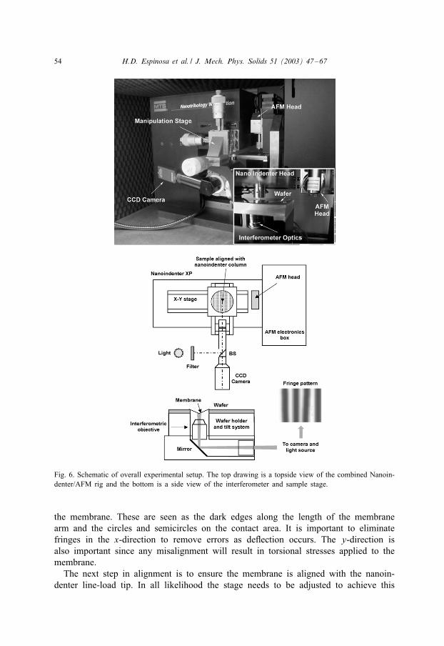
A schematic of the membrane de7ection experimental setup is shown in Figs. 5and 6. It consists of a nanoindenter, to apply load to the center of the membrane from

H.D. Espinosa et al. / J. Mech. Phys. Solids 51 (2003) 47–67 53
PV
Wafer
Optics
MirauMicroscopeObjective
PMPM
θ ∆
LM
Fig. 5. Side view of the MDE test showing vertical load being applied by the nanoindenter, PV, the membranein-plane load, PM, and the position of the Mirau microscope objective.
the top, and a Mirau microscope interferometer positioned directly below the speci-men to independently measure de7ection through the microfabricated die window. Acombined Nanoindenter and atomic force microscope (AFM) apparatus was used inthis investigation to apply a line load to the center of the membranes. The typicalexperimental procedure can be described in three steps. The (rst step is to locate andcharacterize the membrane geometry by means of the optical and scanning capabilitiesof the AFM. Once the pro(le and surface geometry are stored, the wafer is movedto the test position to begin the second step. This is accomplished by means of anx–y translation stage with a positioning accuracy of 1 �m or better. The second stepis the MDE itself. Parameters are set and a drift test is executed. Once the test cri-terion is reached, the membrane is loaded. Simultaneously, the aligned interferometricstation is focused on the back surface of the (lm. The camera is then set to acquiredigital images within a desired period of time. Force and displacement data are storedin the Nanoindenter controller PC, and full-(eld displacements are stored by acquir-ing monochromatic images. Prior to acquiring each set of images, the focus on thesurface is updated to correct for the out-of-plane motion resulting from the downwarddisplacement of the membrane.
The third step of the experiment is data reduction. Using the measured distance be-tween fringes, obtained from the interferometer, and load and de7ection data, obtainedfrom the nanoindenter measurements, Cauchy stress and stretch are independently com-puted.
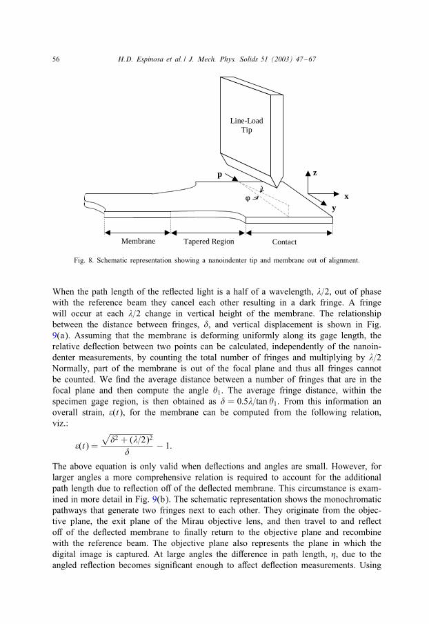
2.3.1. AlignmentIn the MDE it is important to ensure that the membrane is loaded in a uniform
manner to avoid spurious e=ects such as torsional forces and/or errors in true de7ection.This is accomplished by ensuring that the nanoindenter line-load tip, membrane, andinterferometer are all in alignment. The (rst step in the process is to align the membraneand the interferometer. The x- and y-axis rotational adjustments of the interferometerare tuned until all fringes disappear. Fig. 7(a) is an optical image of a membranealigned with the interferometer. Some fringes are present due to the curved surface of
54 H.D. Espinosa et al. / J. Mech. Phys. Solids 51 (2003) 47–67
Fig. 6. Schematic of overall experimental setup. The top drawing is a topside view of the combined Nanoin-denter/AFM rig and the bottom is a side view of the interferometer and sample stage.
the membrane. These are seen as the dark edges along the length of the membranearm and the circles and semicircles on the contact area. It is important to eliminatefringes in the x-direction to remove errors as de7ection occurs. The y-direction isalso important since any misalignment will result in torsional stresses applied to themembrane.
The next step in alignment is to ensure the membrane is aligned with the nanoin-denter line-load tip. In all likelihood the stage needs to be adjusted to achieve this

H.D. Espinosa et al. / J. Mech. Phys. Solids 51 (2003) 47–67 55
Fig. 7. Monochromatic images obtained from the interferometer showing: (a) a membrane perfectly alignedwith the interferometer; (b) a membrane under load in which the nanoindenter tip, membrane, and interfer-ometer are well aligned; note that fringes are developed evenly; and (c) a membrane under load in whichthe tip and membrane are out of alignment, fringes are not developed uniformly.
alignment. We have added two orthogonal cuts and countersink screws to be able totilt the surface of the stage supporting the wafer. De7ecting the membrane by a modestamount in order to develop a few fringes checks alignment. If these fringes developuniformly, noting that they will be slightly curved in the y-direction due to surfacecurvature, then the two are in alignment. If the fringes develop on an angle, then thestage must be adjusted to correctly position the membrane. The di=erence between analigned and misaligned membrane is shown in Fig. 7(b) and (c). The proper directionin which the stage should be rotated around the x-axis is determined by observingthe fringes on the contact area of the membrane. As the tip makes contact with oneside of a misaligned membrane, point “p” in Fig. 8, the opposite side will developfringes because the contact area, being signi(cantly wider than the arms, will twistin the positive z-direction to bring it in contact with the tip and out of the plane ofalignment with the interferometer. Thus, in the case of the schematic in Fig. 8, thestage must be rotated in the negative z-direction along the x-axis. The interferometeris then realigned with the membrane as described above. This process is repeated untilfringes are developed uniformly.
2.3.2. Fringe development and measurementAs the membrane is de7ected by the nanoindenter, the interferometer, which works
based on the Michelson Interferometer principle, records the membrane de7ection byresolving surface fringes. The fringes are a result of phase di=erences of monochro-matic light re7ecting o= the surface by traveling di=erent path lengths to and fromthe membrane. This light is recombined with a reference beam of (xed path length.
56 H.D. Espinosa et al. / J. Mech. Phys. Solids 51 (2003) 47–67
φφ x y
zp
Tapered Region Contact Membrane
Line-LoadTip
Fig. 8. Schematic representation showing a nanoindenter tip and membrane out of alignment.
When the path length of the re7ected light is a half of a wavelength, �=2, out of phasewith the reference beam they cancel each other resulting in a dark fringe. A fringewill occur at each �=2 change in vertical height of the membrane. The relationshipbetween the distance between fringes, �, and vertical displacement is shown in Fig.9(a). Assuming that the membrane is deforming uniformly along its gage length, therelative de7ection between two points can be calculated, independently of the nanoin-denter measurements, by counting the total number of fringes and multiplying by �=2Normally, part of the membrane is out of the focal plane and thus all fringes cannotbe counted. We (nd the average distance between a number of fringes that are in thefocal plane and then compute the angle �1. The average fringe distance, within thespecimen gage region, is then obtained as � = 0:5�=tan �1. From this information anoverall strain, �(t), for the membrane can be computed from the following relation,viz.:
�(t) =
√�2 + (�=2)2
�− 1:
The above equation is only valid when de7ections and angles are small. However, forlarger angles a more comprehensive relation is required to account for the additionalpath length due to re7ection o= of the de7ected membrane. This circumstance is exam-ined in more detail in Fig. 9(b). The schematic representation shows the monochromaticpathways that generate two fringes next to each other. They originate from the objec-tive plane, the exit plane of the Mirau objective lens, and then travel to and re7ecto= of the de7ected membrane to (nally return to the objective plane and recombinewith the reference beam. The objective plane also represents the plane in which thedigital image is captured. At large angles the di=erence in path length, �, due to theangled re7ection becomes signi(cant enough to a=ect de7ection measurements. Using

H.D. Espinosa et al. / J. Mech. Phys. Solids 51 (2003) 47–67 57
Fig. 9. Schematic representation showing the relationship between distance between fringes (�) and verticaldisplacement (a) and the correction in path length, �, to account for the angled re7ection at large values of�1 (b).
geometrical relations, a correction factor can be found to accurately relate the measureddistance between two fringes on the objective plane, �′, with the associated distancebetween fringes at the membrane plane, �, namely,
�= 4�′ cos2 �1 and tan �1 =�=2�:
The (nite strain, s(t), can then be computed with this new �, viz.
s(t) =
√�2 + (�=2)2
�:
By acquiring images at periodic intervals, the de7ection and strain can be mappedas a function of time. Fig. 10 shows a series of acquired digital images and fringedevelopment on a membrane. Between 400 and 425 s, the membrane begins to exhibita large localized plastic deformation, seen as discontinuous fringes, which eventually

58 H.D. Espinosa et al. / J. Mech. Phys. Solids 51 (2003) 47–67
Fig. 10. Composite of monochromatic images obtained from the interferometer at periodic intervals, from0 s to fracture at 456 s.
led to failure. The frame at 456 s shows only the right part of the membrane; the leftpart is out of focus.
Although this measurement of strain is obtained in a local area on the membranesurface, it represents an overall strain for the entire gauged region and is thus, assumedto be uniformly distributed. This type of assumption allows the possibility of edgee=ects to enter the data, however, as mentioned in Section 2.1 the specimens weredesigned with specially tapered regions and suRcient length to remove these e=ectsfrom the gauged region. In fact, tests performed on di=erent specimen lengths providedidentical Young’s modulus, residual stress, and yield stress (see Section 4). In futurestudies, the authors will employ other strain measuring techniques, such as digitalspeckle correlation (DSC), to obtain localized strain data.

H.D. Espinosa et al. / J. Mech. Phys. Solids 51 (2003) 47–67 59
Another aspect of strain measurement stems from the fact that the nanoindenter alsorecords the displacement history of the indenter tip. Much like the interferometer, thisdata also provides an overall strain for the specimen. Both methods yield strain val-ues that match well for small angles of de7ection. However, the nanoindenter methodlacks some key aspects provided by the interferometer data. Primarily, the video im-age of fringe development clearly pinpoints the exact moment of contact between thenanoindenter tip and membrane. Determination of this point via the nanoindenter datais not so accurate with estimation errors resulting in distortions of residual stress andYoung’s modulus. The interferometer also allows veri(cation that the membrane isloaded uniformly in its plane, see Fig. 7. Another advantage is that the onset of shearlocalization, see Fig. 10, and membrane failure are also observed.
3. Data reduction
The data recorded during the MDE test is in raw form and must be processed toobtain in-plane load and stress. The data obtained from a typical test is the Nanoindenterdisplacement in nanometers, load in milli-Newtons, and time in seconds as well as avideo (le of the fringe development recorded in Audio Video Interleave format (.avi).
3.1. Correcting the raw load signature
Reduction of the load data requires two steps. The (rst is the correction of the rawload obtained from the Nanoindenter. The second is the calculation of the membranein-plane load. Besides the response of the membrane, the raw load signature is com-posed of other factors such as: sti=ness of the gantry, sti=ness of the support springs,changes in resistivity of the load coil, and thermal drift of the column. Of these factorsthe e=ect of the gantry sti=ness is considered negligible since it is several orders ofmagnitude larger than the sti=ness of the support springs or membrane. We also assumeload coil resistance variability to be negligible. Thermal drift occurs when the gantryis expanding or contracting as a result of temperature 7uctuations. The (nal e=ect onthe measured load is due to the sti=ness of the support springs. These springs supportthe nanoindenter column and have high sti=ness in the direction perpendicular to thecolumn, to avoid lateral deviations, while in the direction of the column their sti=-ness is approximately 100 N=m. Usually this e=ect is easily accounted for in standardnanoindentation, but in the case of membrane de7ection experiments the load responseof the membrane is one order of magnitude smaller than the springs’ sti=ness. As aresult, a much more accurate procedure is needed.
The combined e=ect of the support spring sti=ness and thermal drift factors resultsin a load response signi(cantly larger than that of the typical membrane with thesti=ness of the support springs being the largest contribution by far. In order to properlyand accurately subtract these e=ects, they must be measured when the tip is not incontact with the membrane. This was accomplished by performing the test in air priorto de7ecting the membrane. It was also determined that this air test needed to beperformed at least four times to elicit an equilibrium and repetitive response from the

60 H.D. Espinosa et al. / J. Mech. Phys. Solids 51 (2003) 47–67
0.01.02.03.04.05.06.07.08.09.0
10.0
0 20000 40000 60000 80000 100000 120000
Displacement (nm)
Loa
d (m
N) Membrane Failure
MembraneRun 2-4 Run 1
Fig. 11. Plot of raw load vs. displacement for air runs (thin lines) and membrane run (thick line). Runs2–4 are close together and appear as one thick line.
0
0.1
0.2
0.3
0.4
0.5
0.6
0.7
0.8
0 10000 20000 30000 40000 50000 60000 70000Displacement (nm)
Loa
d (m
N)
Membrane Load
NanoindenterLoad
Fig. 12. Load–displacement signatures for the corrected nanoindenter vertical load and the computed mem-brane in-plane load.
springs. A typical load-de7ection signature of an air run is shown in Fig. 11. Theresponse appears linear, but in actuality it is slightly nonlinear.
The air tests are immediately followed up by the actual membrane de7ection. Load–de7ection signatures of the membrane and (nal air test are compared to determinethe actual load response of the membrane. First, a polynomial representation of theload–displacement signature of air test is made. In the second step, the polynomial isdirectly subtracted from the membrane vertical load–displacement signature to removethermal drift and spring sti=ness e=ects. Typical membrane vertical load–displacementsignatures of raw and corrected data are shown in Figs. 11 and 12, respectively. Theload response of the membrane is dwarfed by the magnitude of the spring and drifte=ects. At the point of fracture the raw membrane load signature returns to follow thatof the air test.

H.D. Espinosa et al. / J. Mech. Phys. Solids 51 (2003) 47–67 61
3.2. Conversion from nanoindenter vertical load to membrane load
The second processing to the measured vertical load response is geometric in nature,in that, the component of load in the membrane plane (PV), in the direction normal tothe cross section must be computed from the load measured by the nanoindenter column(PM). A schematic of their relationship is shown in Fig. 5. As de7ection increases, sodoes the angle �. By using the de7ection and the initial length of the membrane (Lm),� and PM can be computed at any point during the test from the following equations:
tan �=�LM
and PM =PV
2 sin �:
Fig. 12 shows the di=erence in load signatures between the Nanoindenter (PV) andmembrane loads (PM). The magnitude of the membrane load is signi(cantly largerthan that of the nanoindenter load. This disparity is a result of very small values ofthe sin(�) at low de7ections. At extremely low values of displacement this e=ect isalso observed to magnify the scatter at the low end of resolution for the load cell, i.e.,loads below 10 �N, as seen at the beginning of the membrane load signature. Thisscatter exists in the nanoindenter load as well, but is masked by the small magnitudeof the measured loads. Upon fracture the loads of both signatures do not return to zerosince half of the membrane is still engaged with the nanoindenter tip and is behavingas a cantilever. Once the actual load in the membrane is found, Cauchy stress, �(t),can be computed from
�(t) =PM
A;
where A is the cross-section area of the membrane in the gauge region.
4. Experimental data
4.1. Repeatability
An important feature of every new experimental method is repeatability in the mea-surements. To examine this issue, (ve experiments were performed on membranesof the same size within two wafers of di=erent thickness (T ), 0.5 and 1:0 �m. Theload–de7ection signatures from these thin (lm Au membranes are shown in Fig. 13(a)for T = 0:5 �m and (b) for T = 1:0 �m. The membranes compared all have identicaldimensions; length (LM) = 372 �m, width (W ) = 10 �m. The signatures of each thick-ness are signi(cantly di=erent and result from size e=ects that are clari(ed in part II ofthis article. At small magnitudes of displacement, in both plots, the membranes of eachthickness exhibited identical behavior except for the region of very small displacementswhere the load cell is at its low end of sensitivity. This region corresponds to the earlyelastic deformation regime. As displacement increased, the membranes began to showevidence of plasticity and varying failure behavior. The strong agreement between theload–displacement signatures of the (ve membranes of each thickness indicates that

62 H.D. Espinosa et al. / J. Mech. Phys. Solids 51 (2003) 47–67
0
0.2
0.4
0.6
0.8
1
1.2
1.4
Mem
bran
e L
oad
(mN
)
0
0.1
0.2
0.3
0.4
0.5
0.6
0.7
0.8
0.9
1
Mem
bran
e L
oad
(mN
)
(a)
(b)
0 10000 20000 30000 40000 50000 60000
Displacement (nm)
0 10000 20000 30000 40000 50000
Displacement (nm)
Fig. 13. Membrane load vs. displacement plots of (ve di=erent identically sized membranes with (lmthickness of: (a) 0:5 �m; and (b) 1:0 �m.
the MDE procedure is a repeatable and reliable method to uniformly stretch, much likea direct tensile test, thin (lms and MEMS materials.
4.2. Stress–strain curves
Stress–strain curves for the membranes in Fig. 13 are shown in Fig. 14(a) forT = 0:5 �m and (b) for T = 1:0 �m. Each membrane for both wafers followed iden-tical elastic behavior with a measured Young’s modulus of 53–55 GPa. As with theload–displacement signatures, the stress–strain curves di=er greatly between each thick-ness. The measured modulus is signi(cantly lower than the value of 78 GPa for bulkAu, however, values reported for thin (lm Au have varied from 30 to 78 GPa (Nix,1989). The di=erence may result from the strong 〈1 1 1〉 texture exhibited by thin gold(lms (Harris and King, 1994,1998). The gold (lms used in this study also exhibit astrong 〈1 1 1〉 texture, see Section 3.1 in Part II of this article for further details. Itis known that the Young’s modulus of single crystal gold varies with orientation. Forinstance, E〈111〉 = 117 GPa and E〈1 0 0〉 = 43 GPa (Courtney, 1990). Thus, with 〈1 1 1〉

H.D. Espinosa et al. / J. Mech. Phys. Solids 51 (2003) 47–67 63
0
50
100
150
200
250
300
350
0 0.002 0.004 0.006 0.008 0.01Strain
Stre
ss (
MP
a)
0
10
20
30
40
50
60
70
80
0 0.002 0.004 0.006 0.008 0.01Strain
Stre
ss (
MP
a)
Slope =53-55 GPa
(a)
(b)
Slope = 53-55 GPa
Fig. 14. Stress–strain curves of (ve di=erent, but identically sized membranes with (lm thickness of:(a) 0:5 �m and (b) 1:0 �m.
primarily normal to the (lm surface, the 53–55 GPa measured moduli are realistic. Theuniform behavior of the membranes in the elastic regime lends further support to therepeatability and reliability of the MDE test.
Extrapolation of the elastic regime to the vertical axis provides an estimate of themembrane residual stress. This stress is for the suspended (lm after it has been releasedfrom its substrate. It should not be confused with the residual stress state of the (lmwhile on a substrate. In the case of the examined specimens the residual stress is tensileand in the range 10–12 MPa, see Fig. 14.
Yield stress was found to be approximately 170 MPa for all (ve of the 0:5 �m thickspecimens and 50–55 MPa for the 1:0 �m thick membranes. The elastic regime ofthe 1:0 �m thick specimens is expanded, to illustrate the variability in measured yieldstress, in Fig. 15. It is known that the yield stress of polycrystalline metallic thin (lmsstrongly depends on their crystallographic texture (Thompson, 1993). In part II of thisarticle we report on details of the (lms grain morphology and texture and their e=ecton yield stress. Here we just point to the fact that the scatter in yield stress, in thecase of the 1:0 �m thick membranes is 10% while the change in yield stress due to

64 H.D. Espinosa et al. / J. Mech. Phys. Solids 51 (2003) 47–67
0
10
20
30
40
50
60
70
0 0.0005 0.001 0.0015 0.002Strain
Stre
ss (
MP
a)
Slope = 53-55 GPa
Fig. 15. Expansion of the elastic region for Fig. 14(b).
a change in thickness from 1.0 to 0:5 �m is about 340%! Likewise, the 1 �m thickmembranes show quite interesting post-yield behavior. Upon reaching their yield stress,each membrane began to undergo plastic deformation and quickly began exhibiting in-dividual deformation behavior, especially for the 1:0 �m thick specimens, followed byfailure at varied stresses and strains. The 0:5 �m thick membranes all exhibited sharpchanges in stress and catastrophic failure. Some 1:0 �m thick specimens showed catas-trophic failure after a period of ductility while others showed a progressive reductionto zero stress. Also present in the plastic regime of the 1:0 �m thick specimens aresharp undulations of stress indicating that plastic yielding happened in discrete manner.This feature is very much in contrast to the smooth hardening behavior of bulk metals.
4.3. Membrane size e9ects
Fig. 16 is a load–displacement plot for two di=erent sized membranes. The solid cir-cles (•) represent the same sized membrane presented earlier, length (LM) = 372 �m,width (W ) = 10 �m, thickness (T ) = 1:0 �m, while the open circles (©) representa membrane of dimensions, length (LM) = 674 �m, width (W ) = 20 �m, thickness(T ) = 1:0 �m. Both membranes have identical shapes and thickness, but their geome-tries are at di=erent size scales. It should also be mentioned that they were processedon the same wafer. The load–displacement signatures of the two di=er in some re-spects. The (rst is that the greater cross-section area of the larger membrane resultedin a larger load magnitude, as expected, as well as a greater displacement before failureoccurred. Both membranes appear to have ruptured in a similar manner. The secondnoticeable di=erence between the two sizes is the load behavior at small displacements.In particular, the larger membrane exhibits a di=erent loading behavior until a displace-ment of 15 �m where it abruptly changes its loading response to follow what wouldappear to be the extension of the smaller membrane load–displacement curve.
The stress–strain curves of the two di=erent sized membranes are shown in Fig. 17.As in Fig. 16, the solid circles (•) represent the smaller membrane and the open

H.D. Espinosa et al. / J. Mech. Phys. Solids 51 (2003) 47–67 65
0
0.2
0.4
0.6
0.8
1
1.2
1.4
1.6
0 10000 20000 30000 40000 50000 60000 70000Displacement (nm)
Loa
d (m
N)
( ) LM = 372µm, W=10 µm( ) LM = 674µm, W=20 µm
Fig. 16. Comparison of membrane load–displacement signatures for two di=erently sized membranes; (•)represents the membrane of dimensions length (LM) = 372 �m, width (W ) = 10 �m, thickness (T ) = 1:0 �mand (©) represents the membrane of dimensions length (LM) = 674 �m, width (W ) = 20 �m, thickness(T ) = 1:0 �m.
0
10
20
30
40
50
60
70
80
90
100
0 0.001 0.002 0.003 0.004 0.005 0.006Strain
Stre
ss (
MPa
)
Slope = 53-55 GPa ( ) LM = 372µm, W=10 µm( ) LM = 674µm, W=20 µm
Fig. 17. Comparison of stress–strain curves for the two membranes described in Fig. 16 using correspondingsymbols.
circles (©) represent the larger membrane. Both curves match rather well with identicalYoung’s modulus of 53–55 GPa, identical yield stress of 55 MPa, and similar fracturestresses and strains. Some di=erences in the post-yielding behavior are clearly observedin the stress–strain plots. Further details of size e=ects in gold thin (lms are elucidatedin part II of this work. Further results are presented in part II of this work.
5. Conclusions
A novel chip-level test has been presented to investigate mechanical properties of thin(lms used in the microelectronics industry as well as in the design of MEMS. The main

66 H.D. Espinosa et al. / J. Mech. Phys. Solids 51 (2003) 47–67
advantages of the proposed test and methodology are their simplicity, the independentmeasurement of stress and strain, without recourse to mathematical assumptions ornumerical interpretations of the experiments, and its accuracy and repeatability. Thetechnique can be used to investigate a variety of materials ranging from metals toceramics including piezo-materials, shape memory alloys, ultra-nano-crystalline (lms,etc. By using the specimen ends as electrodes, direct measurement of current–voltage(I–V ) diagrams resulting from the coupling between electrical and mechanical (eldsis feasible.
The MDE test results on Au (lms shows that micron-thick (lms can be testedby direct tension using a properly designed membrane specimen. The equipment em-ployed was shown to possess the sensitivity and control required for such precisemeasurements. Our future work will involve testing Au (lms of various thickness andcross-section areas as well as other materials including membranes with oxide layers,simulating passivation. Investigations will also be performed to further study plasticityand fracture at the submicron scale.
Acknowledgements
The (rst author would like to express his gratitude to John Hutchinson for manyenlightening discussions during HDE sabbatical at Harvard University. This work wassponsored by the National Science Foundation under Career Award No. CMS-9624364and the ORce of Naval Research YIP through Award No. N00014-97-1-0550. Workwas also supported in part by the Nanoscale Science and Engineering Initiative of theNational Science Foundation under NSF Award Number EEC-0118025. Special thanksare due to G. Donahue and V. Diadiuk of the Microsystems Technology Laboratoryat the Massachusetts Institute of Technology for their aid in microfabrication and W.Oliver and B. Peters of MTS Systems Corporation for their assistance in the utilizationof the nanoindenter during this investigation.
References
Chasiotis, I., Knauss, W., 1998. Mechanical properties of thin polysilicon (lms by means of probemicroscopy. Proc. SPIE—Int. Soc. Opt. Eng. 3512, 66–75.
Courtney, T.H., 1990. Mechanical Behavior of Materials. McGraw-Hill, New York, p. 60.Drory, M., Hutchinson, J., 1995. An indentation test for measuring adhesion toughness of thin (lms under
high residual compression with application to diamond (lms. Mater. Res. Soc. Symp. Proc. 383, 173–182.Espinosa, H.D., Fischer, M., Zhu, Y., Lee, S., 2001a. 3-D Computational modeling of RF MEMS switches.
In: Laudon, M., Romanowicz, B. (Eds.), Proceedings of the Fourth International Conference on Modelingand Simulation of Microsystems, pp. 402–405.
Espinosa, H.D., Prorok, B.C., Zhu, Y., Fischer, M., 2001b. An investigation of plasticity in MEMS materials.Proceedings of InterPACK ’01, July 8–13, Kauai, HI, USA.
Espinosa, H.D., Prorok, B.C., Fischer, M., 2001c. A novel experimental technique for testing thin (lmsand MEMS materials. Proceedings of the SEM Annual Conference on Experimental and AppliedMechanics, June 4–6, Portland, OR, pp. 446–449.
Evans, A.G., He, M.Y., Hutchinson, J.W., 1997. E=ect of interface undulations on the thermal fatigue ofthin (lms and scales on metal substrates. Acta Mater. 45, 3543–3554.

H.D. Espinosa et al. / J. Mech. Phys. Solids 51 (2003) 47–67 67
Fischer, M., 1999. MEMS materials testing. Master Thesis. Purdue University, West Lafayette, IN.Harris, K.E., King, A.H., 1994. Localized texture formation and its detection in polycrystalline thin (lms of
gold. Mater. Res. Soc. Symp. Proc. 317, 425–430.Harris, K.E., King, A.H., 1998. Direct observation of di=usional creep via TEM in polycrystalline thin (lms
of gold. Acta Mater. 46, 6195–6203.Huang, H., Spaepen, F., 1996. Measurement of Young’s modulus and Poisson’s ratio of free standing Au/Cu
multilayered thin (lms. Mater. Res. Soc. Symp. Proc. 405, 501–505.Kiesewetter, L., Zhang, J., Houdeau, D., Stecborn, A., 1992. Determination of Young’s modulus of
micromechanical thin (lms using the resonance method. Sensors Actuators A 35, 153–159.Manceau, J., Robert, L., Bastien, F., Oytana, C., Biwersi, S., 1996. Measurement of residual stresses in
a plate using a vibrational technique-application to electrolytic nickel coatings. J. Microelectromech. Syst.5, 243–249.
Nix, W., 1989. Mechanical properties of thin (lms. Metall. Trans. A 20, 2217–2245.Oliver, W., Pharr, G., 1992. An improved technique for determining hardness and elastic modulus using load
and displacement sensing indentation experiments. J. Mater. Res. 7, 1564–1583.Osterberg, P., Senturia, S., 1997. A test chip for MEMS material property measurement using electrostatically
actuated test structures. J. Microelectromech. Syst. 6, 107–118.Sharpe Jr., W., 1995. Elastoplastic stress and strain concentrations. J. Eng. Mater. Technol. 117, 1–7.Sharpe Jr., W., 1996. A new technique for measuring poisson’s ratio of MEMS materials. Mater. Res. Soc.
Symp. Proc. 444, 185–190.Sharpe Jr., W.N., Brown, S., Johnson, G.C., Knauss, W.G., 1998. Round robin tests of modulus and strength
of polysilicon. Mater. Res. Soc. Symp. Proc. 518, 57–65.Small, M., Nix, W., 1992. Analysis of the accuracy of the bulge test in determining the mechanical properties
of thin (lms. J. Mater. Res. 7, 326–335.Small, M., Daniels, B., Clemens, B., Nix, W., 1994. The elastic biaxial modulus of Ag–Pd multilayered thin
(lms using the bulge test. J. Mater. Res. 9, 126–133.Thompson, C., 1993. The yield stress of polycrystalline thin (lms. J. Mater. Res. 8, 237–238.Vlassak, J., Nix, W., 1992. A new bulge test technique for the determination of Young’s modulus and
Poisson’s ratio of thin (lms. J. Mater. Res. 7, 401–413.Yuan, B., Sharpe Jr., W., 1997. Mechanical testing of polysilicon thin (lms with the ISDG. Exp. Tech. 21,
32–35.Zeng, H., Sharpe Jr., W., 1996. A system for measuring biaxial creep strains over short gage lengths. Exp.
Mech. 36, 84–90.
Related Documents