A main frame semiconductor memory for fourth generation computers by THOMAS W. HART, JR., DURRELL W. HILLIS, JOHN MARLEY, ROBERT C. LUTZ and CHARLES R. HOFFMAN MOTOROLA, SPD Phoenix, Arizona INTRODUCTION It has been obvious for several years that Large Scale Integration could be applied to memories. Memories offer several advantages in that a large volume of one type of device can be manufactured, and that the de- sign can be optimized for one application. There exists a wide spectrum of memory product areas with varying size, costs, speed and enviromental performance. Most of these application areas are presently serviced by various forms of magnetic storage. Semiconductor memories have been encroaching into some of these areas. First, the "scratchpad" was re- placed by semiconductor memories yielding a better performance at lower cost. Secondly, the small buffer memories are now being implemented by various forms of semiconductor storage, mainly by MOS shift regis- ters. Large very high speed semiconductor buffers are being built for large systems such as the IBM 360/85 to "effect a hardware performance increase of slower core main memories. It is felt that the advent of an all semiconductor main frame memory is fast approaching. The initial market penetration will be in the high performance area (100-300 ns) replacing flat-film memory designs where costs per bit are quite high. Eventually, most memory application areas will be vulnerable to semi- conductor implementation on a price and performance basis. This paper "ill describe a memory module which will be used as a building block to implement high performance memories in the next generation of com- puters. 479 Jlodule description Under various engineering and marketing con- straints, a module building block concept evolved. This module in its general form .contains 8192 bits. Inter- face to and from the module is performed with standard current-mode logic levels. MECL levels were chosen because that logic family provides the fastest inter- face when connecting many modules into a large mem- 0ry system. Also, most of the customers and potential customers working on high speed systems are using some form of current-mode logic. In any event, it is not dif- ficult to interface from other logic families to MECL levels. . By varying the logical connections to the module, an organization of 8192Xl, 4096X2, 2048X4, or l024X8, can be Figure 1 shows a block diagram of the module. Addressing is binary. Inputs and outputs may be bussed with other modules for expansion of the number of locations in a memory system. No com- plicated timing is necessary to operate the module. When an address is applied, the contents of the speci- fied address will appear at the output terminals within 85 ns and remain until a new address is presented. Writing in a specified location is accomplished by pulsing the write enable line after the address and data have been presented. The module can be cycled every lOOns. The memory module uses p-channel MOS flip-flops for storage. Address decoding, word drive, sense, and digit drive are accomplished with bipolar circuits. This combination results in a low power, low cost From the collection of the Computer History Museum (www.computerhistory.org)

Welcome message from author
This document is posted to help you gain knowledge. Please leave a comment to let me know what you think about it! Share it to your friends and learn new things together.
Transcript

A main frame semiconductor memory
for fourth generation computers
by THOMAS W. HART, JR., DURRELL W. HILLIS, JOHN MARLEY, ROBERT C. LUTZ and CHARLES R. HOFFMAN
MOTOROLA, SPD Phoenix, Arizona
INTRODUCTION
It has been obvious for several years that Large Scale Integration could be applied to memories. Memories offer several advantages in that a large volume of one type of device can be manufactured, and that the design can be optimized for one application. There exists a wide spectrum of memory product areas with varying size, costs, speed and enviromental performance. Most of these application areas are presently serviced by various forms of magnetic storage.
Semiconductor memories have been encroaching into some of these areas. First, the "scratchpad" was replaced by semiconductor memories yielding a better performance at lower cost. Secondly, the small buffer memories are now being implemented by various forms of semiconductor storage, mainly by MOS shift registers. Large very high speed semiconductor buffers are being built for large systems such as the IBM 360/85 to "effect a hardware performance increase of slower core main memories.
It is felt that the advent of an all semiconductor main frame memory is fast approaching. The initial market penetration will be in the high performance area (100-300 ns) replacing flat-film memory designs where costs per bit are quite high. Eventually, most memory application areas will be vulnerable to semiconductor implementation on a price and performance basis. This paper "ill describe a memory module which will be used as a building block to implement high performance memories in the next generation of computers.
479
Jlodule description
Under various engineering and marketing constraints, a module building block concept evolved. This module in its general form . contains 8192 bits. Interface to and from the module is performed with standard current-mode logic levels. MECL levels were chosen because that logic family provides the fastest interface when connecting many modules into a large mem-0ry system. Also, most of the customers and potential customers working on high speed systems are using some form of current-mode logic. In any event, it is not difficult to interface from other logic families to MECL levels. .
By varying the logical connections to the module, an organization of 8192Xl, 4096X2, 2048X4, or l024X8, can be obtain~d. Figure 1 shows a block diagram of the module. Addressing is binary. Inputs and outputs may be bussed with other modules for expansion of the number of locations in a memory system. No complicated timing is necessary to operate the module. When an address is applied, the contents of the specified address will appear at the output terminals within 85 ns and remain until a new address is presented. Writing in a specified location is accomplished by pulsing the write enable line after the address and data have been presented. The module can be cycled every lOOns.
The memory module uses p-channel MOS flip-flops for storage. Address decoding, word drive, sense, and digit drive are accomplished with bipolar circuits. This combination results in a low power, low cost
From the collection of the Computer History Museum (www.computerhistory.org)
480 Fall Joint Computer Conference, 1969
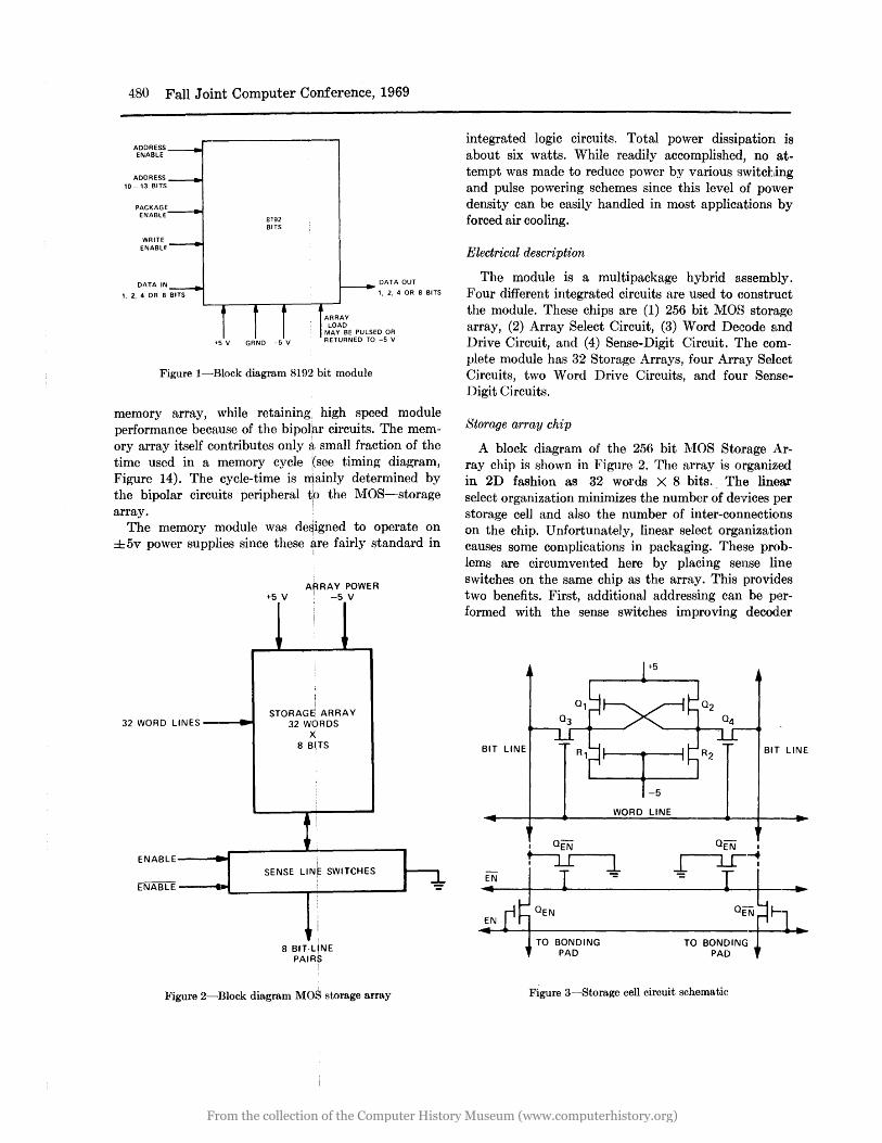
----------------------------------------------------------ADDRESS ENABLE
ADDRESS 10 - 13 BITS
1, 2, 4 OR 8 BITS
8192 BITS
+5 V GRND -5 V
ARRAY LOAD
DATA OUT
1, 2, 4 OR 8 BITS
MAY BE PULSED OR RETURNED TO -5 V
Figure I-Block diagram 8192 bit module
memory array, while retaining, high speed module performance because of the bipolar circuits. The memory array itself contributes only a small fraction of the time used in a memory cycle (see timing diagram, Figure 14). The cycle-time is mainly determined by the bipolar circuits peripheral ~o the lVIOS-storage array.
The memory module was de~igned to operate on ±5v power supplies since these ~re fairly standard in
32 WORD L INES --
ENABLE ---
ARRAY POWER +5 V '-5 V
11
;
i STORAGE ARRAY
32 WORDS X
8 BITS
• !
, SENSE lIN~ SWITCHES
:
1. : ~
8 BIT-L!NE PAIRS
Figure 2-Block diagram M OS storage array
Il:
integrated logic circuits. Total power dissipation is about six watts. While readily accomplished, no attempt was made to reduce power by various Bwitching and pulse powering schemes since this level of power density can be easily handled in most applic~ttions by forced air cooling.
Electrical description
The module is a multi package hybrid assembly. Four different integrated circuits are used to eonstruct the module. These chips are (1) 256 bit MOS storage array, (2) Array Select Circuit, (3) Word Deeode and Drive Circuit, and (4) Sense-Digit Circuit. The complete module has 32 Storage Arrays, four Array Select Circuits, two Word Drive Circuits, and four SenseDigit Circuits.
Storage array chip
A block diagram of the 256 bit lVIOS Sto:rage Array chip is shown in Figure 2. The array is organized in 2D fashion as 32 words X 8 bits. _ The linoar select organization minimizes the number of devices per storage cell and also the number of inter-connections on the chip. Unfortunately, linear select organization causes some complications in packaging. These problems are circumvented here by placing sense line switches on the same chip as the array. This provides two benefits. First, additional addressing can be plerformed with the sense switches improving decodler
BIT LINE BIT LINE
-5
~ __ --+_ __ ~------~W~O~R~D~L~IN~E~------~--+_---~
EN ~----~--~~---------------------4_---~---___.
~E.N-4--~--__ --------------------------~--r1_.. TO BONDING
PAD TO BONDING
PAD
Figure 3-Storage cell circuit schematic
From the collection of the Computer History Museum (www.computerhistory.org)

efficiency. Second, the internal capacitance of the bit-lines can be isolated from the external bit lines by the sense switches, substantially improving the sense loop time constant.
A schematic of a storage cell and the MOS senseswitches at the end of the bit line is shown in Figure 3. Ql and Q2 are the active devices of the flip-flop, RI and R2 are the flip-flop load devices, and Q3 and Q4 are the series gating devices which connect a selected
Main Frame Semiconductor Memory 481
cell to the bit line pair. Each bit line has a transistor QEN in series with the connection to the bonding pad and a transistor QEN which terminates the bit line to ground when QEN is on. The geometries of the active devices are designed to provide a sense current of 80 microamperes under worst case processing and operating conditions. The load resistor device geometries determine the standby power dissipation of the chip which in this case is about 40 milliwatts.
Figure 4-256 Bit M08 storage array
From the collection of the Computer History Museum (www.computerhistory.org)
482 Fall Joint Computer Conference, 1969
Figure 4 is a photomicrograph of the chip. The dimensions of the chip are 138 mils X 141 mils. A low threshold process using < 100> material is used. The substrate serves as the buss for the +5 volt supply.
One layer of metal interconnection is used. A high concentration P-diffusion (15-20in/square) is used for crossunders so as to minimize series resistance. In the layout the bit lines have no crossunders. The word lines have nine crossunders. The resistance of these crossunders and capacitance associated with the word gates on the memory cell form :an RC delay line. In this design the delay is about 2.5 us.
Chip 8election circuit
A bipolar circuit which decodes three binary bits is used to select one of eight MOS Storage Array Chips. Each of the output driver stages provides the complimentary signals EN and EN necessary to drive the sense switches on the MOS Storage Array. Additional inputs to the·· chip-selection Cu;cuit are provided to select groups of eight arrays.
Emitter Coupled Logic (EC~) input signals are translated to saturated logic which is referenced to the negative supply (-5.0). The complimentary output stages provide logic levels near the positive (+5) and negative (-5) supplies for driving the MOS sense switches. Block and Logic Diagrams are shown in Figures 5 and 6.
Memory package
Eight MOS Storage Array chips and one chip selection circuit are contained in a 1.2·5 inch square memory package. Interconnection of these nine chips is made by a beam lead laminate as described later in this paper. Each memory package contains a total of 2048 bits
THREE-BIT( ADDRESS
ADDRESS ENAB LE (2)
+5 V
GRND
-5 V
~ )TOCHI.='
ENABLE ) TO CHIP =8 'E"fiJ'A'BIT
Figure 5-Chip select circuit
ADDRESS ENABLE ADDRESS INPUT
ADDRESS ENABLE ADDRESS INPUT
ADDRESS INPUT
TO ENABLE & ENABLE LINES OF MEMORY .ARRAY CHIPS
~""""'---='-~E A E EE'
Figure 6-Chip select circuit logic
as shown in Figure 7. Four such packages form 'the storage portion of the 8192 bit memory modlllle. This assembly of four packages results in a total capacitance buildup of 250 picofarads on the word lineH and 70 picofarads on the sense-digit lines.
Decoding word driver
Selection of the storage array word lines i:3 accomplished by a bipolar circuit which decodes fowr address bits and drives one out of sixteen word lines. As in the Chip Selection Circuit, ECL input signals are transla'ted to saturated logic whose outputs provide . logic levels near + 5 and - 5 volts. Block and logic diagrams are shown in Figures 8 and 9. Two of these chips are packaged in a 1.25 inch square package similar to -the memory array package except that interconnection within the package is made with a thick film met:Etlization and wire bonds. Two address enable inputs are provided. One is used as a master enable and 1~he other is used as a one bit decode to select one or 1~he
16 WORD lINES-~-.t
8 BIT·lINE PAIRS
256 WORDS X 8 BITS
NINE CHIP HYBRID ASS'BLY
-5 V GRND +5 V
..... --16 WORD LINES
.... --ENAEILE
..... --ARR.Ay POWER
Figure 7-Memory package
From the collection of the Computer History Museum (www.computerhistory.org)

DECODING WORD
DRIVER
'1 WORD LINE OUTPUTS
2 ADDRESS ENABLES----t-t
ENABLE
ADDRESS INPUT
ENABLE
ADDRESS INPUT
ADDRESS INPUT
ADDRESS INPUT
-5 V GRND +5 V
Figure 8-Decoding word driver chip
TO WORD SELECT LINES OF MEMORY ARRAY PLANES "
......... ----+lI---++-~+-""*__t+- - - - - - -~----~~~-~-+~~------
Figure 9-Decoding word driver chip logic
other of two Decoding Word Driver chips sharing the same package. A block diagram of this package is shown in Figure 10.
Sense amplijier"digit driver
The sense amplifier"digit driver subassembly contains four identical sense amplifier~digit driver integrated circuit chips. Each chip receives and sends read and write signals to the MOS storage array, accepts EeL level data input and data enable signals, and generates EeL data output signals.
The purpose of each chip is, of course, twofold.
16 WOF.lD LINES ..... --4 1---..... 16 WORD LINES
7 BIT ADDRESS---t~
-5 V GRND +5 V
Figure l~Decoding word driver package
Main Fr~me Semiconductor Memory 483
First! . when it ha~b~en properly enabled for writing, it must transmita'-W:r..it~ signal to appropriate bites) of the selected word ·in the storage array. Second, when properly enabled, it must sense the storage cell currents. of the s~lected word and translate them to EeL signals at the data output terminals.
The logic diagram shown in Figure 11 is functionally equivalent to the sense amplifier-digit driver circuit. In addition to showing the basic sense amplifier, digit driver, and gate blocks of the sense amplifier-digit driver chip, Figure 11 also shows the existence of a bit line recovery circuit. The purpose of this circuit is to rapidly return all bit line voltages to zero, immediately after each write operation.
To thoroughly understand the sense amplifierdigit driver logical organization, consider the sequence of events which must occur to perform the read and write operations.
To accomplish a write operation, the desired input data is placed at the DATA IN terminals of the chip. The data is enabled by a coincidence of logical zeroes at the DATA ENABLE inputs. When the WRITE ENABLE input is forced to a logical zero, one of the bit line voltage drivers in each half of the circuit drives one line of each bit line pair to approximately +4v. This voltage impressed on a bit line accomplishes the write in the storage array. The leading negative edge of the WRITE ENABLE signal also sets the recovery . circuit flip-flop. The following positive edge of the WRITE EN ABLE signal turns the digit driver (8) off and turns the recovery circuit driver on. When recovery of all bit lines is accomplished, the recovery circuit flip-flop resets and the recovery circuit driver is shut off .. Both the digit driver and the recovery circuit driver are designed to exhibit a very high output
NOTES THE NUMBERED BLOCKS CORRESPOND TO THE FOLLOWING 1 BIT LINE VOLTAGE DRIVER. 2. SENSE AMPLIFIER, 3 VOLTAGE COMPARATOR, 4 BIT LINE RECOVERY CURRENT DRIVER
Figure ll-Sense amplifier/digit driver chip logic
From the collection of the Computer History Museum (www.computerhistory.org)
484 Fall Joint Computer C?nference, 1969 ---------------------------ti ------___________________________________________________________ __
I
impedance when off, such that they do not interfere with the read operation.
Reading is accomplished by enabling either one or both halves of the chip with ~he DATA E~ABLE signals. If the WRITE ENAB.t.E is held at logical one, the bit line currents flow into the sense amplifier inputs. The sensed information i is made available at the DATA OUT terminals. Since the I/O signals are EeL, uncommitted emitter outputs are used so that wired OR'ing of the positive going output signals is possible.
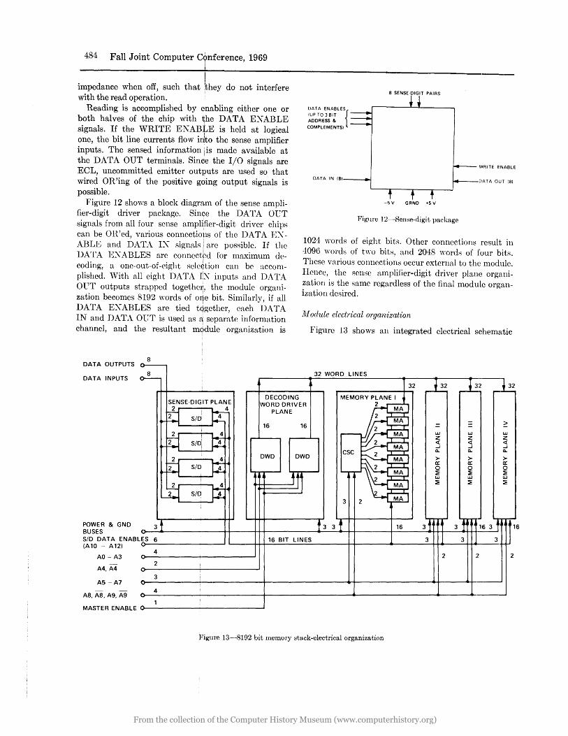
Figure 12 shows a block diagram of the sense amplifier-digit driver package. Since the DATA OUT signals from all four sense amplifier-digit driver chips can be OR'ed, various connectioilS of the DATA EXABLE and DATA 1:\ signals j are possible. If the DATA EXABLES are connectPd for maximum decoding, a one-out-of-eight seleJtioll can be accomplished. \Vith all eight DATA IX inputs and DATA OeT outputs strapped togethell, the module organization becomes 8192 words of one bit. Similarly, if all DATA EXABLES are tied together, each DATA IN and DATA OeT is used as a separate information channel, and the resultant mqdule organization is
8 DAT A OUTPUTS
8 DATA INPUTS
DATA ENABLES
(UPT03BIT { ADDRESS &
COMPLEMENTS)
DATA IN (8) __ ~
8 SENSE-DIGIT PAIRS
-5 V GRND +5 V
Figure 12-Sense-digit package
WRITE ENABLE
DATA OUT (8)
1024 words of eight bits. Other connections result ill "1096 words of two bits, and 2048 words of four bits. These various connections occur external to the module. lIenee, the sense amplifier-digit driver plane organization is the same regardless of the final module organization desired.
]1,[ odule elcctr'ical organization
Figure 13 shows an integrated electrical slChematic
32 WORD LINES
32
SENSE-DIG'IT PLANE 2 4
DECODING WORD DRIVER
PLANE
POWER & GND BUSES
3
4
16 16
DWD DWD
= -w w Z Z <t: <t: ..J ..J ~ ~
:> :> ex: ex: 0 0 ~ ~ w w ~ ~
SID DATA ENABLES 6 L-_-4++...;1:.:6_B::.:I:..;.T.....::.L1;,,;,.N:..;:E:.::S ____ ++ ___ -4 ____ 3-t-t4 __ 3-1-1~ 3 (A 10 - A 12) 0------------'
AO- A3
A4.A4
A5-A7
A8. A8. A9, A9
4
2
3
4
MASTER ENABLE o----------------~
Figure 13-8192 bit memory stack-electrical organization
2
2: w Z <t: ..J ~
:> ex: 0 ~ w ~
2
From the collection of the Computer History Museum (www.computerhistory.org)

of the 8192 bit memory module. Notice that the package-to-package connections are accomplished by means of long parallel busses or rails which are formed when the six packages are stacked. Although these rails must be broken in some places to define the interconnection, no. jumper wires, etc., need be added.
There are three distinct methods of addressing shown in Figure 13:
1. Address bits AO, AI, A2, and A3 are bussed in parallel to the two decoding word driver chips (DWD). Since each DWD is a one out of sixteen decoder, an additional address bit (A4-A4) is decoded on the enable inputs of the DWD's. Hence, the decoding word driver package functions as a one out of thirtytwo decoder, selecting only one of 32 word select lines to enable in the memory array. Note that all word select lines in the thirty-two lVIOS array chips are wired in parallel.
Address bits A5, A6, A7 drive the chip select circuits (CSC) in the memory array packages. The CSC drives the ENABLE and ENABLE of memory array's sense line switch, and select one of the eight array chips with each memory array package. To complete the selection of an eight bit word on one lVIOS array one of the four memory planes must be uniquely enabled. The two enable inputs of each chip select circuit, (CSC) are connected to address bit A8 and A9 or their complement~ to perform the plane selection. Connection to the correct two signals is accomplished by providing A8, A8, A9, and A9 at the edge of all memory array packages and breaking the bus connection with two of the signals.
These ten bits (AO-A9) select one eight bit word out of the 1024 word array. Subdivision of the eight bit word into four, two, or one bit words is accomplished by strapping lines (DEI-DE6) together in specific combinations. The sense amplifier package can accept zero, one, two, or three address bits depending on the module organization desired.
Once a single eight bit word in the storage array has been addressed,· sixteen low impedance paths (eight pairs of bit lines) exist between the four sense amplifier-digit driver chips and the eight MOS array cells. Reading is accomplished by sensing the storage cell currents while holding the bit lines at approximately ground; writing by forcing selected bit lines to a positive voltage.
In addition to the standard I/O and address channels, a DWD ENABLE and/or CSC ENABLE are brought out to allow for further addressing or for eliminating skew in the address signals.
Main Frame Semiconductor Memory 485
Module timing
Figure 14 is a timing diagram of the 8192 bit module. The diagram is organized into three sections: (1) the basic addressing and enabling common to both read and write cycles. (2) the basic read cycle, and (3) the basic write cycle. The diagram illustrates how the various propagation and charging delays add to form the minimum cycle times.
Since all word select and bit lines are parallel connected to all thirty-two array chips, the capacitances associated with these lines are high (approximately 250 pf on word lines, 70 pf on bit lines). Therefore, charging times become a significant portion of the memory cycle time.
The labels on the diagram are generally self explanatory. The comments below explain some of the special features shown.
Notice that if desired, the sense amplifier-digit driver data enable inputs (DE1-DE6) can arrive at the module terminals some 15 ns later than the address signal (AO-A9). Therefore, additional levels of decoding logic may be added in series with these inputs without slowing the cycle time.
During the read cycle the sensed information must be strobed out toward the end of the cycle, as the information on the sense amplifier-digit driver DATA OUTPUTS prior to that time is the stored information in the previously addressed location or undefined. Bit line recovery after writing is overlapped into the next cycle.
Packaging
The 8192 Bit l\1emory lVlodule is an assembly of four 2048 Bit iHemory Array packages, a word driver packa~~e, and a sense digit package. Each of these packages are 1.25 inches square with 17 leads on 50 mil centers on each side. The electrical organization is such that the packages can be stacked one above the other with the leads bussed. After assembly and test of the individual packages are complete, the individual leads are cut and formed. The packages are then placed in a mechanical holder, and wave soldered one side at a time. A molded header is then mechanically and electrically attached to the base of the stacked assembly of packages,. The header includes guide slots so that the ends of the ribbon leads can be inserted into a simple etched wiring board nested within the header. The 42 signal pins of the header are arranged in a 1.6 inch square on 100 mil centers. This choice of pin form factor permits established printed circuit board technology to be employed by the user.
From the collection of the Computer History Museum (www.computerhistory.org)

486 Fall Joint Computer CotIference, 1969
ADDRE~S LINES TO ~I,~~~~~~~~~~.~~~~_~~~~~~~~~~~~~ l)WD iii esc IAII-'I'I' -----X
~D~W~D~.~C~~P~: .. R~O~P~D~E~LA~Y~7<E7&~-----~~--~--~~~~~~~~~~~
INTERNAL WORD & - LINE CHARGING _ ~. ARRAY fN,'\HLE LlN[S .
Ii 'rr=MEMORY ARRAY PROP DELAY
~1~~~~R~U~~~~~S \ If ADDRESSING & DATA ENABLE
\~;'0~5D~D'E~ EN~n~ : o-r-f ~ Bn UNE CHARGE t-HIT LINE VOLTAGES E'j I ~~fy=.I/--~--------1~ DURING READ _~~
SA:DD DATA OUTPUTS I ~ SENSE AMP. b-' I -=-lSENSE AMPDELAYt;::
~DUUR1ING D~8~D DATA: ENABLE DELAYF-I;;o-ss.BLE~;LSE-R~AD).r --', -----r-B-ASIC READ CYCLE
l XTERNAL STROBE FOR READING
I I --~----~---------~
SA'DO DATA INPUTS =* : -----DURING WRITE ,D11 DIB. '
; -; WRITE ENABLE DELAY ~IN. WRITE BASIC
I i I ~ \ ENJABLE DELAY I WRITE CYCLE
WRITE ENA~LE DELAY~ I ~, I--BIT LINE RECOVERYl
WHITE ENABLE PULSE
BIT LINE VOLTAGES DURING WRITE I . tcELL WRITING TlME1 --~
I I ' I I I I I I , I I I • tins) o 10' 20 30 40 50 60 10 80 90 100 110
Figure 14-Timing diagram - 8192 bit MOS stack memory
The heat generated by this module is approximately 6 watts. The volume of the module assembly including the 42 pin header and piug is 1: 75 X 1. 75 X 2.0 inches or six cubic inches. 0nerational bit density is thus over 1300 bits per cubic inch. It is felt that these two counteracting factors are fai~ly well balanced to each other by this module design cqncept.
Package interconnect
The Sense-Digit and Word Driver packages are simply one -l~yer thick film met~l patterned ceramic packages with connections being made with flying wire leads. The memory array p~ckage is much more densely populated and uses a neW- technology of inter-connect. .
Interconnect technologies curtently available are multilayer ceramic, multi-layer s~rface deposition, or multi-layer "add on" laminate. i Ceramic multi-layer was not selected for three reason.. The high dielectric constant of alumina raises the di~tributed capacitance to levels which threaten system! speed requirements. The many vias required for i~tra-Iayer connection cannot be placed on close enough qenters to be compatible with the desired cell densitie~. Finally, the length of buried conductors used for power distribution exhibit higher resistance than is desired for low noise level operation. '
Use of multi-layer surface depositions on a :suitable package substrate has been avoided because of yield problems of dielectric defects in the presence Qif many crossovers, and the presence of deposition interfaces at each via buildup location. Surface deposition of a single low-impedance thick film pattern on the package substrate has been utilized for power distribution to the IC chips within the container.
Interconnect laminate
The interconnection is implemented by a separate part· called an interconnect laminate. The dielectric core of this laminate is 1 mil polyimide film and ,exhibits the following characteristics:
1. Physically and electrically stable dielectric through the range of -65:lC to +450:l0.
2. Dielectric constant of 3.5. 3. Pinhole free and a voltage breakdown rating
of 7000 volts at one mil thickness. Through a series of precisely-registered artwork and photo-chemical cycles, the two-layer X-Y interconnections are formed to the following standards:
1. Via size of 1.5 to 2.0 mils diameter on seven mil centers.
2. Via lands or caps are 4 X 5 mils. 3. Conductor widths are three mils and conductors
are spaced on five mil centers.
From the collection of the Computer History Museum (www.computerhistory.org)
Main Frame Semiconductor Memory 487
UPPER ~6 MIU j VIA CONDUCTORS .\J. ~ .:. 6 MILS I DIE~ic~RIC
P [/ZllZ)Z/*/® I @--:_~W-.....L-_~ LOWER
CONDUCTOR
I.C. CHIP
--~------ ----- ----- ------ ------ ------ ------ ------ ------
Figure 15-Interconnect cross-section
4. Conductors on both sides and the vias are electroplated as a single structure having no metallurgical interfaces at the vias.
These standards of fabrication provide an interconnect system which is compact and comparable in geometry details to the bond pads and spacing used by MOTOROLA on its IC chip products. Capacitance measurements of typical center conductors to the sum of grounded neighboring conductors, using the above dimensional and material standards, read about 2.15 picofarads per inch of length while dc resistance of typical conductors measures 0.40 ohms per inch of length.
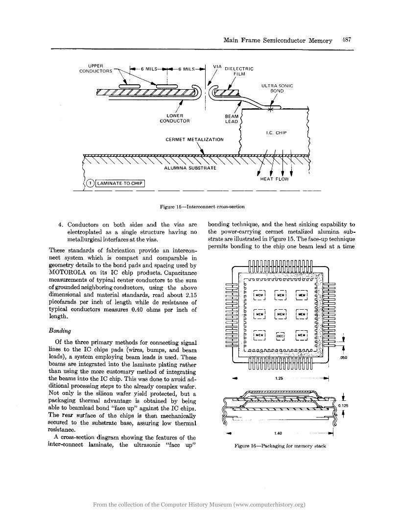
Bonding
Of the three primary methods for connecting signal lines to the IC chips pads (wires, bumps, and beam leads), a system employing beam leads is used. These beams are integrated into the laminate plating rather than using the more customary method of integrating the beams into the IC chip. This was done to avoid additional processing steps to the already complex wafer. Not only is the silicon wafer yield protected, but a packaging thermal advantage is obtained by being able to beamlead bond "face up" against the IC chips. The rear surface of the chips is then mechanically secured to the substrate base, assuring low thermal resistance.
A cross-section diagram showing the features of the inter-connect laminate, the ultrasonic "face up"
bonding technique, and the heat sinking capability to the power-carrying cermet metalized alumina substrate are illustrated in Figure 15. The face-up technique permits bonding to the chip one beam lead at a time
1.25 ~i
~:~>!(:$:i:~~5 1.40 ------~
Figure 16-Packaging for memory stack
From the collection of the Computer History Museum (www.computerhistory.org)
488 Fall Joint Computer Conference, 1969
or one chip at a time. It also perrpits quite stringent quality control measures to be imMemented since the beams can be examined individually~
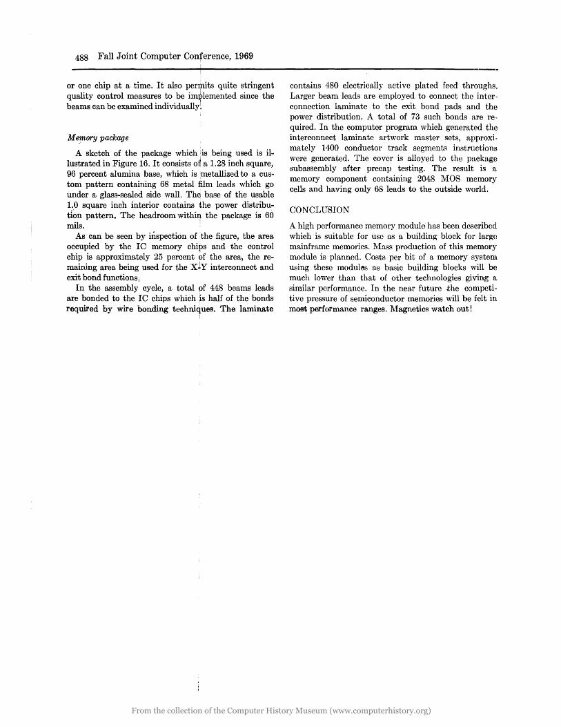
Memory package
A sketch of the package which ·is being used is illustrated in Figure 16. It consists of a 1.28 inch square, 96 percent alumina base, which is metallized to a custom pattern containing 68 metal film leads which go under a glass-sealed side wall. The base of the usable 1.0 square inch interior contains the power distributl~n pattern. The headroom within the package is 60 mils.
As can be seen by inspection of the figure, the area occupied by the IC memory chips and the control chip is approximately 25 percent of the area, the remaining area being used for the XJy interconnect and exit bond functions!
In the assembly cycle, a total of 448 beams leads are bonded to the IC chips which is half of the bonds required by wire bonding techniq.ues. The laminate
contains 480 electrically active plated feed throughs. Larger beam leads are employed to connect the inter·· connection laminate to the exit bond pads and the power distribution. A total of 73 such bonds are re·· quired. In the computer program which generated the interconnect laminate artwork master sets, approxi. mately 1400 conductor track segments instructions were generated. The cover is alloyed to the package subassembly after precap testing. The result is a, memory component containing 2048 MOS memory cells and having only 68 leads to the outside world.
CONCLUSION
A high performance memory module has been des.cribed which is suitable for use as a building block for large mainframe memories. 1\tlass production of this memory module is planned. Costs per bit of a memory system using these modules as basic building blocks will be much lower than that of other technologies giving fL
similar performance. In the near future the competi. tive pressure of semiconductor memories will be felt in moat performance ranges. Magnetics watch out!
From the collection of the Computer History Museum (www.computerhistory.org)
Related Documents