Rincon-Mora and Allen 1 A Low Voltage, Low Quiescent Current, Low Drop-out Regulator Gabriel Alfonso Rincon-Mora and Phillip E. Allen School of Electrical and Computer Engineering Georgia Institute of Technology Atlanta, GA 30332-0250 Abstract The demand for low voltage, low drop-out (LDO) regulators is increasing because of the growing demand for portable electronics, i.e., cellular phones, pagers, laptops, etc. LDOs are used coherently with dc-dc converters as well as standalone parts. In power supply systems, they are typically cascaded onto switching regulators to suppress noise and provide a low noise output. The need for low voltage is innate to portable low power devices and corroborated by lower breakdown voltages resulting from reductions in feature size. Low quiescent current in a battery operated system is an intrinsic performance parameter because it partially determines battery life. This paper discusses some techniques that enable the practical realizations of low quiescent current LDOs at low voltages and in existing technologies. The proposed circuit exploits the frequency response dependence on load-current to minimize quiescent current flow. Moreover, the output current capabilities of MOS power transistors are enhanced and drop-out voltages are decreased for a given device size. Other applications, like dc-dc converters, can also reap the benefits of these enhanced MOS devices. An LDO prototype incorporating the aforementioned techniques was fabricated. The circuit was operable down to input voltages of 1 V with a zero-load quiescent current flow of 23 μA. Moreover, the regulator provided 18 and 50 mA of output current at input voltages of 1 and 1.2 V respectively. I. Introduction The low drop-out nature of the regulator makes it appropriate for use in many applications, namely, automotive, portable, industrial, and medical applications [1]. The

Welcome message from author
This document is posted to help you gain knowledge. Please leave a comment to let me know what you think about it! Share it to your friends and learn new things together.
Transcript
Rincon-Mora and Allen 1
A Low Voltage, Low Quiescent Current, Low Drop-out Regulator
Gabriel Alfonso Rincon-Mora and Phillip E. Allen
School of Electrical and Computer Engineering
Georgia Institute of Technology
Atlanta, GA 30332-0250
Abstract
The demand for low voltage, low drop-out (LDO) regulators is increasing because of the
growing demand for portable electronics, i.e., cellular phones, pagers, laptops, etc. LDOs are
used coherently with dc-dc converters as well as standalone parts. In power supply systems, they
are typically cascaded onto switching regulators to suppress noise and provide a low noise
output. The need for low voltage is innate to portable low power devices and corroborated by
lower breakdown voltages resulting from reductions in feature size. Low quiescent current in a
battery operated system is an intrinsic performance parameter because it partially determines
battery life. This paper discusses some techniques that enable the practical realizations of low
quiescent current LDOs at low voltages and in existing technologies. The proposed circuit
exploits the frequency response dependence on load-current to minimize quiescent current flow.
Moreover, the output current capabilities of MOS power transistors are enhanced and drop-out
voltages are decreased for a given device size. Other applications, like dc-dc converters, can also
reap the benefits of these enhanced MOS devices. An LDO prototype incorporating the
aforementioned techniques was fabricated. The circuit was operable down to input voltages of 1
V with a zero-load quiescent current flow of 23 µA. Moreover, the regulator provided 18 and 50
mA of output current at input voltages of 1 and 1.2 V respectively.
I. Introduction
The low drop-out nature of the regulator makes it appropriate for use in many
applications, namely, automotive, portable, industrial, and medical applications [1]. The

Rincon-Mora and Allen 2
automotive industry requires LDOs to power up digital circuits, especially during cold-crank
conditions where the battery voltage can be below 6 V. The increasing demand, however, is
especially apparent in mobile battery operated products, such as cellular phones, pagers, camera
recorders, and laptops [2]. In a cellular phone, for instance, switching regulators are used to
boost up the voltage but LDOs are cascaded in series to suppress the inherent noise associated
with switchers. LDOs benefit from working with low input voltages because power
consumption is minimized accordingly, P = ILoad * Vin. Low voltage and low quiescent current
are intrinsic circuit characteristics for increased battery efficiency and longevity [3]. Low
voltage operation is also a consequence of process technology. This is because isolation barriers
decrease as the component densities per unit area increase thereby exhibiting lower breakdown
voltages [4, 5]. Therefore, low power and finer lithography require regulators to operate at low
voltages, produce precise output voltages, and have characteristically lower quiescent current
flow [5]. By the year 2004, the power supply voltage is expected to be as low as 0.9 V in 0.14 µ
m technologies [5, 6]. Drop-out voltages also need to be minimized to maximize dynamic range
within a given power supply voltage. This is because the signal-to-noise ratio typically
decreases as the power supply voltages decrease while noise remains constant [7]. Lastly,
financial considerations also require that these circuits be realized in relatively simple processes,
such as standard CMOS, bipolar, and inexpensive biCMOS technologies [8]. An example of the
relatively inexpensive biCMOS process is the 2 µm MOSIS technology (information is available
through the internet at http://www.isi.edu/mosis). This is a vanilla CMOS process with an added
p-base layer to realize vertical NPN transistors. Figure 1 illustrates the general components of a
typical low drop-out regulator, namely, an error amplifier, a pass device, a reference circuit, a
feedback network, and some loading elements. The associated gate capacitance of the pass
device is depicted as Cpar.
II. Current Efficient Buffer
2.1 Current Efficiency

Rincon-Mora and Allen 3
Current efficiency is an important characteristic of battery powered products. It is
defined as the ratio of the load-current to the total battery drain current, which is comprised of
load-current (ILoad) and the quiescent current (Iq) of the regulator,
currentLoad
Load qEfficiency I
I I=
+. (1)
Current efficiency determines how much the lifetime of the battery is degraded by the mere
existence of the regulator. Battery life is restricted by the total battery current drain. During
conditions where the load-current is much greater than the quiescent current, operation lifetime is
essentially determined by the load-current, which is an inevitable characteristic of linear
regulators. On the other hand, the effects of quiescent current on battery life are most prevalent
during low load-current conditions when current efficiency is low. For many applications, high
load-current is usually a temporary condition whereas the opposite is true for low load-currents.
As a result, current efficiency plays a pivotal role in designing battery powered supplies. The
two performance specifications that predominantly limit the current efficiency of low drop-out
regulators are maximum load-current and transient output voltage variation requirements.
Typically, more quiescent current flow is necessary for improved performance in these areas.
2.2 Challenges
Output current and input voltage range directly affect the characteristics of the pass
element in the regulator, which define the current requirements of the error amplifier. As the
maximum load-current specification increases, the size of the pass device necessarily increases.
Consequently, the amplifier's load capacitance, Cpar in Figure 1, increases. This affects the
circuit's frequency performance by reducing the value of the parasitic pole present at the output
of the amplifier [9]. Therefore, phase-margin degrades and stability may be compromised unless
the output impedance of the amplifier is reduced accordingly. As a result, more current in the
buffer stage of the amplifier is required, be it a voltage follower or a more complicated circuit
architecture. In a similar manner, low input voltages require that MOS pass device structures

Rincon-Mora and Allen 4
increase in size and thus yield the same negative effects on frequency response and quiescent
current as just described. This is because the gate drive decreases as the input voltages decrease
thereby demanding larger MOS pass elements to drive high output currents.
Further limits to low quiescent current arise from the transient requirements of the
regulator, namely, the permissible output voltage variation in response to a maximum load-
current step swing. The output voltage variation is determined by the response time of the
circuit, the specified load-current, and the output capacitor [9]. The worst-case response time
corresponds to the maximum output voltage variation. This time limitation is determined by the
closed-loop bandwidth of the system and the output slew-rate current of the error amplifier [9].
These characteristic requirements become more difficult to realize as the size of the parasitic
capacitor at the output of the amplifier (Cpar) increases, which results from low voltage operation
and/or increased output current specifications. Consequently, the quiescent current of the
amplifier's gain stage is limited by a bandwidth minimum while the quiescent current of the
amplifier's buffer stage is limited by the slew-rate current required to drive Cpar.
2.3 Proposed Circuit Topology
A topology that achieves good current efficiency performance is illustrated in Figure 2.
The operation revolves around sensing the output current of the regulator and feeding back a
ratio of the current to the slew-rate limited node of the circuit. Transistor Mps sources a fraction
of the current flowing through the output transistor Mpo. During low load-current conditions,
the current fed back (Iboost) is negligible thereby yielding high overall current efficiency and not
aggravating battery life. Consequently, the current through the emitter follower is simply Ibias
when load-current is low. During high load-current conditions, the current through the emitter
follower is increased by Iboost, which is no longer negligible. The resulting increase in quiescent
current has an insignificant impact on current efficiency because the load-current is, at this point,
much greater in magnitude. However, the increase in current in the buffer stage aids the circuit
by pushing the parasitic pole associated with Cpar (P3) to higher frequencies and by increasing
the current available for slew-rate conditions. Thus, the biasing conditions for the case of zero

Rincon-Mora and Allen 5
load-current can be designed to utilize a minimum amount of current, which yields maximum
current efficiency and prolonged battery life.
Frequency Response: When the load-current is low, the magnitude of the system's
dominant pole (P1), determined by the output capacitor and the output impedance of the pass
device, is also low [10]. This is because the output impedance of the pass device is inversely
proportional to the current flowing through it,
11
2 2P
C RICo o pass
Load
o≈ ≈
−πλπ
, (2)
where Co is the output capacitance, Ro-pass is the output resistance of Mpo, λ is the channel
length modulation parameter, and ILoad is the load-current. Consequently, the unity gain
frequency (UGF) is at low frequencies when the load-current is low, which relaxes the
requirement of the parasitic pole at the output of the error amplifier (P3) to be approximately
greater than or equal to the minimum unity gain frequency (UGFmin). This corresponds to a
phase margin of approximately 45 to 90 ° with an associated design equation of
no load currentnpnP
g
CIV C
UGFm
par
bias
t par− −
≈ = ≥3 2 2π πmin , (3)
where gmnpn is the transconductance of the emitter follower and Vt is the thermal voltage. As
load-current increases, however, the dominant pole increases linearly and consequently so does
the UGF. The open-loop gain (Av) is inversely proportional to the square root of the load
current,
v amp mp o passLoad
Load LoadA A g R
II I
≈ ∝ =−1 , (4)

Rincon-Mora and Allen 6
where Aamp is the gain of the error amplifier while gmp and Ro-pass are the transconductance and
the output resistance of the pass device respectively. Since the dominant pole (P1) increases
faster than the gain decreases with load-current, the unity gain frequency increases as the load-
current increases (equations (2) and (4)). These consequential effects of load-current on
frequency response are graphically illustrated in Figure 3. Zero Z1 and pole P2 are defined by
the output capacitor (Co), associated electrical series resistance (ESR) of Co, and the bypass
capacitors (Cb) shown in Figure 1 [9]. Therefore, the parasitic pole (P3) is also required to
increase with load-current, which is achieved by the load dependent boost current. This is
apparent from the following equation,
3 2 2 2P
g
CI IV C
I kIV C
NPNm
par
bias boost
t par
bias Load
t par≈ =
+≈
+
π π π, (5)
where k corresponds to a constant mirror ratio, i.e., 1/1500 for Figure 2. The circuit can be
designed such that P3 increases at a faster rate than the UGF with respect to load-current. This
results in the following relation,
33
12 2− −= ≈ ≥ ≈ >rateLoad t par
rateo
rateP PI
kV C
PC
UGF∂∂ π
λ
π (6)
or kV CCt par
o≥λ
, (7)
where P3-rate, P1-rate, and UGFrate are the rates with respect to load-current of pole P3, pole P1,
and the unity gain frequency respectively. Thus, current efficiency can be maximized to
accommodate the load dependent requirements of P3. If the load dependence of P3 is not
incorporated into the circuit, then more current than necessary is used during low load-current
conditions. The frequency response behavior was confirmed through simulations.

Rincon-Mora and Allen 7
Transient Response: The circuit of Figure 2 exhibits the transient response illustrated in
Figure 4 depicted as trace "a" where a maximum load-current step swing is applied to the load.
One of the parameters that determines the maximum output voltage variation is the response time
(Δt1) required for the system to react and may be expressed as
11 1
ΔΔ
tBW
tBW
CVIcl
srcl
parsr
≈ + = + , (8)
where BWcl is the closed-loop bandwidth of the system, ΔV is the voltage change associated
with Cpar, and Isr is the output slew-rate current of the error amplifier [9]. However, the slew-
rate current is not constant for the circuit proposed, Isr = Ibias + kIboost. As a result, a slew-rate
condition does not aptly describe the operation of the circuit at hand. During a load-current
transition from zero to maximum value, the response time of the circuit is dominated by the
bandwidth of the system and the transient response of the buffer stage. In particular, the
response time is composed of the time required for the amplifier to respond (tamp), for the sense
PMOS transistor (Mps) to start conducting current (tMps-on), for the positive feedback circuit to
latch up (tlatch-up), and for the output PMOS device (Mpo) to conduct the load-current (tMpo).
This is represented by the following equation,
11
Δt t t t tBW
t tamp Mps on latch up Mpocl
Mps on latch up≈ + + + ≈ + +− − − − , (9)
where BWcl is the closed-loop bandwidth of the system (approximately (tamp + tMpo)-1). The
composite buffer stage is essentially a localized positive feedback circuit. The system is stable
because the positive feedback gain is less than one. Consequently, the circuit attempts to latch
up until the output transistor is fully turned on; at which point, the error amplifier forces the
circuit back into the linear region. As a result, the performance tradeoffs between the slew-rate
and the quiescent current requirements of typical LDOs are circumvented. For instance, if the
parasitic capacitance (Cpar) is 200 pF, the source to gate voltage change required for the output

Rincon-Mora and Allen 8
PMOS transistor (ΔVsg) is 0.5 V, the bandwidth of the system is 1 MHz, and the response time is
limited to be less than 5 µs, then the slew-rate current (Isr = Ibias) required is approximately 25 µ
A (equation (8)). For the case of the circuit in Figure 2, a dc current bias (Ibias) of only 1 µA can
provide the same performance. The dominant factor of the new Δt1 is the time required for the
sense transistor (Mps) to go from being off to sub-threshold and finally to strong inversion.
Figure 4 illustrates the simulation results showing the effect of the presence of boost element
Mps in the circuit shown in Figure 2 on the output voltage, for the same biasing conditions. In
this case, the load-current is stepped from zero to a maximum of 50 mA in 1 ns. It is observed
that the output voltage variation is lower for the circuit implementing the current efficient buffer
resulting from a reduction in response time. This does not come at the expense of additional
quiescent current flow during zero load-current conditions. Consequently, current efficiency and
battery life are maximized.
III. Current Boosting
3.1 Challenge
As the power supply voltages decrease, the gate drive available for the PMOS pass
device decreases. As a result, the aspect ratio of the power transistor needs to be increased to
provide acceptable levels of output current. However, the parasitic gate capacitance also
increases as the size of the PMOS transistor increases. This constitutes an increase in Cpar in
Figure 1, which pulls the parasitic pole (P3) down to lower frequencies. Consequently, the phase
margin of the system is degraded and stability may be compromised. This presents to be a
problem when working in a low quiescent current environment.
3.2 Boosting Technique
One way to improve gate drive without increasing input voltage or device size is by
forward biasing the source to bulk junction of the PMOS pass device. This results in a reduction
of threshold voltage, commonly referred as the bulk effect phenomenon. The threshold voltage
(Vth) is described by
Rincon-Mora and Allen 9
| | | |th to f sb fV V V= + − −γ φ φ2 2 , (10)
where |Vto| is |Vth| at a source to bulk voltage (Vsb) of zero, γ is the body bias coefficient, and |φf|
is the bulk Fermi potential [11]. Consequently, the threshold voltage decreases as Vsb increases
thereby effectively increasing the gate drive of the power PMOS transistor (pass device).
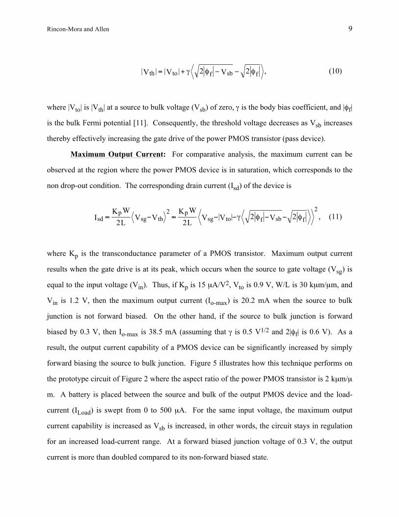
Maximum Output Current: For comparative analysis, the maximum current can be
observed at the region where the power PMOS device is in saturation, which corresponds to the
non drop-out condition. The corresponding drain current (Isd) of the device is
sdp
sg thp
sg to f sb fIK WL V V
K WL V V V≈ − ≈ − − − −
2 22 2
2 2| | γ φ φ , (11)
where Kp is the transconductance parameter of a PMOS transistor. Maximum output current
results when the gate drive is at its peak, which occurs when the source to gate voltage (Vsg) is
equal to the input voltage (Vin). Thus, if Kp is 15 µA/V2, Vto is 0.9 V, W/L is 30 kµm/µm, and
Vin is 1.2 V, then the maximum output current (Io-max) is 20.2 mA when the source to bulk
junction is not forward biased. On the other hand, if the source to bulk junction is forward
biased by 0.3 V, then Io-max is 38.5 mA (assuming that γ is 0.5 V1/2 and 2|φf| is 0.6 V). As a
result, the output current capability of a PMOS device can be significantly increased by simply
forward biasing the source to bulk junction. Figure 5 illustrates how this technique performs on
the prototype circuit of Figure 2 where the aspect ratio of the power PMOS transistor is 2 kµm/µ
m. A battery is placed between the source and bulk of the output PMOS device and the load-
current (ILoad) is swept from 0 to 500 µA. For the same input voltage, the maximum output
current capability is increased as Vsb is increased, in other words, the circuit stays in regulation
for an increased load-current range. At a forward biased junction voltage of 0.3 V, the output
current is more than doubled compared to its non-forward biased state.
Rincon-Mora and Allen 10
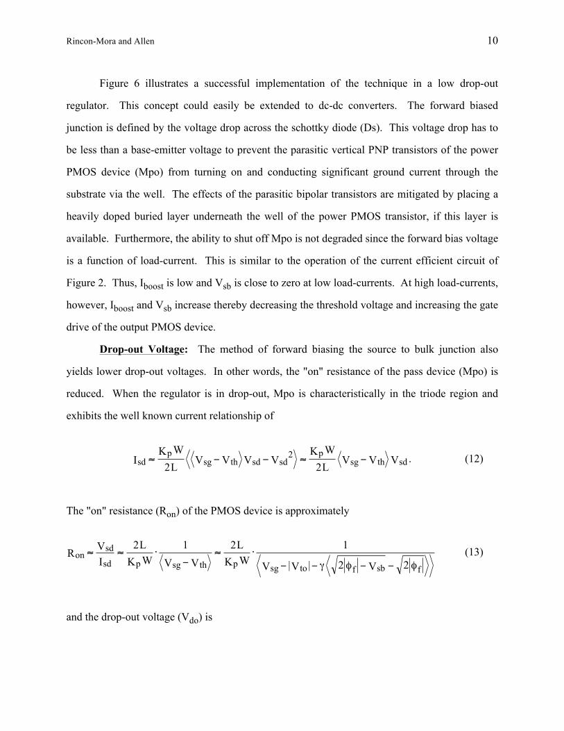
Figure 6 illustrates a successful implementation of the technique in a low drop-out
regulator. This concept could easily be extended to dc-dc converters. The forward biased
junction is defined by the voltage drop across the schottky diode (Ds). This voltage drop has to
be less than a base-emitter voltage to prevent the parasitic vertical PNP transistors of the power
PMOS device (Mpo) from turning on and conducting significant ground current through the
substrate via the well. The effects of the parasitic bipolar transistors are mitigated by placing a
heavily doped buried layer underneath the well of the power PMOS transistor, if this layer is
available. Furthermore, the ability to shut off Mpo is not degraded since the forward bias voltage
is a function of load-current. This is similar to the operation of the current efficient circuit of
Figure 2. Thus, Iboost is low and Vsb is close to zero at low load-currents. At high load-currents,
however, Iboost and Vsb increase thereby decreasing the threshold voltage and increasing the gate
drive of the output PMOS device.
Drop-out Voltage: The method of forward biasing the source to bulk junction also
yields lower drop-out voltages. In other words, the "on" resistance of the pass device (Mpo) is
reduced. When the regulator is in drop-out, Mpo is characteristically in the triode region and
exhibits the well known current relationship of
sdp
sg th sd sdp
sg th sdIK WL V V V V
K WL V V V≈ − − ≈ −
2 22 . (12)
The "on" resistance (Ron) of the PMOS device is approximately
onsd
sd p sg th p sg to f sb f
R VI
LK W V V
LK W V V V
≈ ≈ ⋅−
≈ ⋅− − − −
2 1 2 1
2 2| | γ φ φ (13)
and the drop-out voltage (Vdo) is

Rincon-Mora and Allen 11
do on Loadp
Load
sg to f sb f
V R IL
K WI
V V V≈ ≈ ⋅
− − − −
2
2 2| | γ φ φ. (14)
Thus, if Kp is 15 µA/V2, Vto is 0.9 V, W/L is 30 kµm/µm, Vin is 1.2 V, and ILoad is 20 mA, then
the drop-out voltage is 296 mV (corresponding to 14.8 Ω) when the source to bulk junction is not
forward biased. However, if the source to bulk junction is forward biased by 0.3 V, then Vdo
becomes 216 mV (corresponding to 10.8 Ω) assuming that γ is 0.5 V1/2 and 2|φf| is 0.6 V. There
is a theoretical improvement of approximately 27 %. Figure 7 illustrates the effects of forward
biasing the source to bulk junction on the drop-out performance of the prototype circuit of Figure
6 where the aspect ratio of Mpo is 2 kµm/µm. There is an experimental improvement of roughly
67 % with a forward bias voltage of 0.49 V.
Frequency Response: During low load-current conditions, the current through the sense
transistor (Mps) and consequently the current through the schottky diode (Ds) is negligible. This
is because of the high mirror ratio of the output and the sense transistor, Mpo and Mps in Figure
6. However, Mps and Ds start conducting appreciable current at higher load-currents.
Therefore, these elements constitute another ac signal path for the system. The effect of this path
manifests itself through the transconductance of the pass device (gmp) in the open-loop gain
response. The effective transconductance of the composite pass device of the circuit in Figure 6
can be described as
mp m omx d mb o
b dm o mx d mb og g
g r gsC r
g g r g≈ ++
≤ +−−
− −1, (15)
where gm-o is the transconductance of Mpo, rd is the impedance of the diode Ds, Cb is the total
bulk capacitance of Mpo and Mps, gmb-o is the channel conductance of the bulk of Mpo,
mb osd
sb
psg th
f sbm o
f sbg I
VK WL V V
Vg
V− −= ≈ −
−=
−
∂∂
γ
φ
γ
φ2 2 2 2, (16)

Rincon-Mora and Allen 12
and gmx is mxm s m n
m ng
g gg
= − −
−
2
1, (17)
where gm-s, gm-n1, and gm-n2 are the transconductances of Mps, Mn1, and Mn2 respectively. As
a result of the high mirror ratio between Mpo and Mps, the effective transconductance of the
pass device (gmp) is virtually unaffected by the current boosting technique, i.e., gmp ≈ gm-o. This
can be illustrated by assuming that W/Lo is 30 kµm/µm, W/Ls is 20 µm/µm, ILoad is 50 mA, and
Mn1/Mn2 have a 1:1 mirror ratio; the effective transconductance of the composite power PMOS
transistor is approximately gm-o (1 + 0.05) at dc, where rd ≈ Vt/Idiode, Kp = 15 µA/V2, γ = 0.5
V1/2, 2|φf| = 0.6 V, and Vsb = 0.3 V.
IV. Circuit Design
The problems of low voltage operation emerge in the form of headroom, common mode
range, dynamic range, and voltage swings. Appropriate design techniques must be implemented
to approach the practical low voltage limits of a given process technology. Some of the
techniques that are generally recommended are complementary input amplifiers and common
source [emitter] gain stages. On the other hand, some of the discouraged techniques are
unnecessary cascoding, Darlington configurations, and source [emitter] followers [7]. At the
end, however, the choice of circuit topology and configuration depends on the specific
application and the process technology. The theoretical headroom limit of low voltage operation
is a transistor stack of one diode and one non-diode connected device (Vgs[Vbe] + Vds[Vce]),
which is approximately between 0.9 and 1.1 V in most of today's standard technologies.
The theoretical headroom limit of low voltage for the MOSIS 2 µm n-well technology
with an added p-base layer is roughly 1 - 1.1 V (corresponding to Vsg-pmos + Vds-nmos). The
threshold voltage of MOS devices is roughly between 0.88 and 0.9 V. The same process
technology also offers vertical NPN transistors; however, the respective saturation voltage is
large as a consequence of high collector series resistance. The absence of a highly doped buried

Rincon-Mora and Allen 13
layer prevents this series resistance from decreasing to more favorable levels. Consequently,
NPN saturation voltages are avoided in transistor stacks that define the low voltage headroom
limit. The circuit design of the amplifier can be partitioned into the output buffer and the gain
stage.
The idea of the buffer is to isolate the large capacitor associated with the gate of the
power PMOS transistor from the large resistance of the output of the gain stage. As a result, the
buffer needs low input capacitance and low output impedance. Furthermore, the output voltage
swing needs to extend from as low as possible to the point where the pass device is shut off (Vds
≤ Vo-swing ≤ Vin - 0.7 V). The lower limit is defined to provide maximum gate drive for the pass
element (PMOS transistor). On the other hand, the upper limit is set by the voltage necessary to
shut off the pass device, in other words, extend to just beyond the threshold voltage. This can be
accomplished by a class "A" NPN emitter follower stage. This assumes that the output swing of
the gain stage includes the positive power supply, approximately Vin - Vsd.
The gain stage of the amplifier needs a relatively small common mode range and an
output swing that includes the positive supply voltage. The common mode range is defined
around the reference voltage (Vref), which, in turn, can be designed to be almost any value [12].
The low voltage, current-mode bandgap reference topology of [13] illustrates how this can be
done. As a result, the best device choice for a low voltage differential pair is the NPN transistor
(for the case of MOSIS). This is because its base-emitter voltage drop is roughly 0.6 - 0.7 V
whereas the gate to source voltage of MOS devices is approximately 0.9 V. Thus, a 0.85 - 0.9 V
reference is necessary to accommodate the voltage headroom requirements of the NPN
differential pair in a low voltage environment.
The choice of amplifier topology, however, is limited if the theoretical low voltage limit
is to be approached (Vsg + Vds). The single stage, five-transistor amplifier shown in Figure 8 (a)
is simple enough to yield good frequency response for a given amount of quiescent current flow.
However, a regular current mirror load presents a problem for low voltage operation. A regular
mirror load, as seen in the figure, yields a transistor stack whose associated voltage drop is Vsg +

Rincon-Mora and Allen 14
Vce + Vds, which is limited by approximately 1.4 - 1.5 V in the MOSIS technology. Therefore, a
different low voltage mirror load that yields the theoretical low voltage limit for the MOSIS
technology is proposed (Vsg + Vds ≈ 1 - 1.1 V), as illustrated in Figure 8 (b). It is basically a
mirror with an emitter follower level shift. The circuit operates properly because the base-
emitter voltage drop of the NPN transistor is less than the source to gate voltage of the PMOS
device. The current through the NPN transistor is designed such that the parasitic pole at the
gate of the PMOS device is at high frequencies. This parasitic pole (Pparasitic) is approximated to
be
parasiticm
gsP
g
Cnpn≈ ⋅
212π
, (18)
where gmnpn is the transconductance of the NPN transistor and Cgs is the gate to source
capacitance of each PMOS transistor in the mirror. Among the amplifiers in Figure 8, this
topology exhibits the best systematic offset performance because the voltages at the collector of
both NPN transistors in the differential pair are the same, Vin - Vsg + Vbe. This results because
the voltage at the input of the buffer stage (or output of the gain stage) is defined by a PMOS
pass device and an emitter follower, as seen in the current efficient buffer shown in Figure 2.
Another possible circuit topology for the amplifier is that of a folded architecture, Figure 8 (c).
This circuit also works properly at the theoretical limit of Vgs + Vsd (equivalent to Vsg + Vds).
However, systematic offset performance for this circuit is poor. Furthermore, bandwidth
performance per given total quiescent current flow is not as favorable as that of the circuit shown
in Figure 8 (b) because there are more current sensitive transistor paths to ground.
V. Experimental Results and Discussion
Figure 9 illustrates the final integrated circuit design of the low voltage, low drop-out
(LDO) regulator. The circuit was fabricated in MOSIS CMOS 2 µm technology with an added
p-base layer. The schottky diode was not included in the layout but instead implemented

Rincon-Mora and Allen 15
discretely. The aspect ratio of the power device Mpo is 30 kµm/µm. The LDO produced a
maximum output current of 18 and 50 mA at input voltages of 1 and 1.2 V. The circuit achieved
approximately a 65 % output current improvement over its non-current boosted counterpart, as
shown in Figure 10. The quiescent current flow was 23 µA at zero load-current and 230 µA at
50 mA of load-current, illustrated in Figure 11. The maximum quiescent current at full load was
higher than expected by simulations, approximately 180 µA higher. This is because of the
effects of the large voltage drop across the schottky diode on the parasitic vertical PNP
transistors inherent in the PMOS structure. This can be improved by increasing the diode's area
and/or by placing a heavily doped buried layer (unavailable in MOSIS) underneath the power
PMOS transistor. The line regulation performance of the LDO was 4 mV / 3.8 V. Moreover, the
circuit achieved a load regulation of 19 mV / 50 mA. The drop-out voltage at 60 mA of load-
current was 232 mV, which corresponds to a 17 % improvement over its non current boosted
version, Figure 12. Figure 13 shows the maximum transient output voltage variation resulting
from a sudden load-current pulse (zero to 50 mA), approximately 19 mV (83 % improvement
over the same circuit but without the aid of Mps in Figure 9). The settling time of the LDO
response without Mps is appreciably longer, illustrated by the large overshoot of trace A. This is
attributed to decreased phase margin resulting from the parasitic pole being at low frequencies
(consequence of low bias current through the emitter follower of the buffer). Table 1 gives a
summary of the performance parameters of the low voltage LDO.
VI. Conclusion
A low voltage, low quiescent current, low drop-out regulator has been designed and
implemented. Low quiescent current flow is especially important in portable products where the
total current drain determines battery life. The regulator worked down to 1 V yielding an output
current of 18 mA with 23 µA of quiescent current at zero load-current. At 1.2 V, the circuit was
able to provide 50 mA of output current with 230 µA of quiescent current. Two significant
contributions, current efficient buffer and current boosted pass device, made the low voltage

Rincon-Mora and Allen 16
design viable for battery powered circuits. Both techniques take advantage of the availability of
a sense element that provides a linearly load dependent current. This is intrinsic for low
quiescent current flow during low load-current conditions. The resulting circuit takes maximum
advantage of the transistors utilized to yield low component count and low overall ground
current. Furthermore, the current boosting technique can be readily implemented in applications
requiring low switch-on resistors, i.e., dc-dc converters. In conclusion, some techniques have
been developed and verified that allow the design of low drop-out regulators under existing
technologies to meet today's and tomorrow's low voltage market demands.

Rincon-Mora and Allen 17
References
[1] F. Goodenough, "Off-Line and One-Cell IC Converters Up Efficiency," Electronic Design, pp. 55-64, June 27, 1994. [2] T. Regan, "Low Dropout Linear Regulators Improve Automotive And Battery- Powered Systems," Powerconversion and Intelligent Motion, pp. 65-69, February 1990. [3] J. Wong, "A Low-Noise Low Drop-Out Regulator for Portable Equipment," Powerconversion and Intelligent Motion, pp. 38-43, May 1990. [4] M. Ismail and T. Fiez, Analog VLSI Signal and Information Processing. New York: McGraw-Hill, Inc., 1994. [5] F. Goodenough, "Fast LDOs And Switchers Provide Sub-5-V Power," Electronic Design, pp. 65-74, September 5, 1995. [6] F. Goodenough, "Power-Supply Rails Plummet and Proliferate," Electronic Design, pp. 51-55, July 24, 1995. [7] A. Matsuzawa, "Low Voltage Mixed Analog/Digital Circuit Design for Portable Equipment," 1993 Symposium on VLSI Circuits Digest of Technical Papers, pp. 49-54, 1993. [8] K.M. Tham and K. Nagaraj, "A Low Supply Voltage High PSRR Voltage Reference in CMOS Process," IEEE Journal of Solid-State Circuits, vol. 30 #5, pp. 586-590, May 1995. [9] G.A. Rincon-Mora and P.E. Allen, "Study and Design of Low Drop-out Regulators," submitted to IEEE Transactions on Circuits and Systems. [10] M. Kay, "Design and Analysis of an LDO Voltage Regulator with a PMOS Power Device," Preliminary paper pending publication, Texas Instruments. [11] J.P. Uyemura, Fundamentals of MOS Digital Integrated Circuits. Massachusetts: Addison-Wesley, 1988. [12] G.A. Rincon-Mora and P.E. Allen, "A Novel Low Voltage, Micro-Power Curvature Corrected Bandgap Reference," submitted to IEEE Journal of Solid-State Circuits. [13] M. Gunawan et. al., "A Curvature-Corrected Low-Voltage Bandgap Reference," IEEE Journal of Solid-State Circuits, vol. 28 #6, pp. 667-670, June 1993.

Rincon-Mora and Allen 18
Table 1. Performance summary.
LDO LDO w/o Current Boost
LDO w/o Trans. Boost
Iquiescent @ no-load 23 µA 23 µA 23 µA Iquiescent-max 230 µA 50 µA 200 µA
Io-max @ Vin=1.2V 50 mA 32 mA 50 mA @ Vin=1V 18 mA 8 mA 18 mA Line Reg. 4 mV / 3.8 V 3 mV / 3.67 V 4 mV / 3.8 V Load Reg. 19 mV / 50mA 12 mV / 30 mA 19 mV / 50mA
Vdrop-out @ 60mA 232 mV 280 mV 232 mV Ron 3.9 Ω 4.7 Ω 3.9 Ω
ΔVo for ILoad=pulse (0 to 50mA)
19 mV 19 mV 148 mV
Voffset @ ILoad=1mA
4 mV 4 mV 4 mV
Chip area (not including schottky diode) 1103 µm x 1250 µm

Rincon-Mora and Allen 19
Figure Captions
Figure 1. Typical low drop-out regulator topology.
Figure 2. Current efficient LDO buffer stage.
Figure 3. System frequency response as a function of load-current. Figure 4. LDO output voltage variation with and without the boost element Mps in the current efficient buffer stage.
Figure 5. Maximum load-current performance of the current boost enhancement.
Figure 6. LDO with current boosting capabilities.
Figure 7. Drop-out voltage performance of the current boost topology.
Figure 8. Amplifier topologies.
Figure 9. Low voltage LDO.
Figure 10. Load regulation performance.
Figure 11. Quiescent current as a function of load-current.
Figure 12. Drop-out voltage performance at 60 mA of load-current. Figure 13. Output voltage variation (Traces A & B - without and with the transient boost) resulting from a load-current pulse train (Trace C - 0 to 50 mA).

Rincon-Mora and Allen 20
Figure 1. Typical low drop-out regulator topology.
µΑ∼
Figure 2. Current efficient LDO buffer stage.

Rincon-Mora and Allen 21
Figure 3. System frequency response as a function of load-current.
LDO5 - Transient Response
T ime [s]
0.800.850.900.951.001.051.101.151.20
-10E-3
00E+0
10E-3
20E-3
30E-3
40E-3
50E-3Simulation Results - With and Without Boost Element Mps
Trace a => Vout with MpsTrace b => Vout without Mps
Load-current
a
b
Figure 4. LDO output voltage variation with and without the boost element Mps in the current efficient buffer stage.

Rincon-Mora and Allen 22
Current Boost Enhancement
ILoad [A]
00.10.20.30.40.50.60.70.80.9
1
0.0E+0 1.0E-4 2.0E-4 3.0E-4 4.0E-4 5.0E-4
Vsb=0, 50m, 100m, 150m, 200m, 250m, 300mV
LDO Test - Experimental Results
W/ L=2k
Vsb=0V
Vsb=300mV
Figure 5. Maximum load-current performance of the current boost enhancement.
Figure 6. LDO with current boosting capabilities.

Rincon-Mora and Allen 23
Current Boost - Drop-Out Voltage
Vin [V]
0.5
0.7
0.9
1.1
1.3
1.5
1.7
1.45 1.5 1.55 1.6 1.65 1.7
Vin
Vsb=0 Vdo(1.61V)=58mV w/ Vsb=0
LDO Test - Experimental Results
ILoad = 200uA
W/ L=2k
Vdo(1.61V)=18mV w/ Vsb=0.49V
Vsb=0.49V (Schottky)
Figure 7. Drop-out voltage performance of the current boost topology.
∼
Figure 8. Amplifier topologies.

Rincon-Mora and Allen 24
Figure 9. Low voltage LDO.
LDO3 - Load Regulation
ILoad [A]
00.10.20.30.40.50.60.70.80.9
1
0.0E+0 1.0E-2 2.0E-2 3.0E-2 4.0E-2 5.0E-2 6.0E-2
Experimental Results - With & Without Current Boosting
Vdd=1V Vdd=1.2V
Vdd=1.2V
Vdd=1V
w/ Iboost
w/ o Iboostw/ o Iboost
w/ Iboost
LDR=19mV / 50mA
LDR=7mV / 18mA
Figure 10. Load regulation performance.

Rincon-Mora and Allen 25
LDO3 - Quiescent Current
ILoad [A]
0.0E+0
5.0E-5
1.0E-4
1.5E-4
2.0E-4
2.5E-4
00E+0 10E-3 20E-3 30E-3 40E-3 50E-3 60E-3
Experimental Results - With & Without Current Boosting
Iq=23uA @ ILoad=0
Vin = 1.2V & Vref = 0.9V
Iq-max=230uA
w/ Iboost
w/ o Iboost
Figure 11. Quiescent current as a function of load-current.
LDO3 - Drop-out Voltage
Vin [V]
1.2
1.3
1.4
1.5
1.6
1.7
1.8
1.4 1.5 1.6 1.7 1.8 1.9 2
Experimental Results - With & Without Current Boosting
Vin
Vout w/ o Iboost
Vout w/ IboostVdo=232mV @ Vin=1.71V
Vdo=280mV @ Vin=1.76V
ILoad=60mA
Figure 12. Drop-out voltage performance at 60 mA of load-current.

Rincon-Mora and Allen 26
A
B
C
Figure 13. Output voltage variation (Traces A & B - without and with the transient boost) resulting from a load-current pulse train (Trace C - 0 to 50 mA).
Related Documents