A Low Power 10 GHz Phase Locked Loop for Radar Applications Implemented in 0.13 μm SiGe Technology Except where reference is made to the work of others, the work described in this thesis is my own or was done in collaboration with my advisory committee. This thesis does not include proprietary or classified information. William Souder Certificate of Approval: Stuart Wentworth Associate Professor Electrical and Computer Engineering Auburn University Fa Foster Dai, Chair Professor Electrical and Computer Engineering Auburn University Robert Dean Assistant Professor Electrical and Computer Engineering Auburn University George T. Flowers Dean Graduate School Auburn University

Welcome message from author
This document is posted to help you gain knowledge. Please leave a comment to let me know what you think about it! Share it to your friends and learn new things together.
Transcript
A Low Power 10 GHz Phase Locked Loop for Radar Applications
Implemented in 0.13 µm SiGe Technology
Except where reference is made to the work of others, the work described in this thesis ismy own or was done in collaboration with my advisory committee. This thesis does not
include proprietary or classified information.
William Souder
Certificate of Approval:
Stuart WentworthAssociate ProfessorElectrical and Computer EngineeringAuburn University
Fa Foster Dai, ChairProfessorElectrical and Computer EngineeringAuburn University
Robert DeanAssistant ProfessorElectrical and Computer EngineeringAuburn University
George T. FlowersDeanGraduate SchoolAuburn University
A Low Power 10 GHz Phase Locked Loop for Radar Applications
Implemented in 0.13 µm SiGe Technology
William Souder
A Thesis
Submitted to
the Graduate Faculty of
Auburn University
in Partial Fulfillment of the
Requirements for the
Degree of
Master of Science
Auburn, AlabamaMay 9, 2009
A Low Power 10 GHz Phase Locked Loop for Radar Applications
Implemented in 0.13 µm SiGe Technology
William Souder
Permission is granted to Auburn University to make copies of this thesis at itsdiscretion, upon the request of individuals or institutions and at
their expense. The author reserves all publication rights.
Signature of Author
Date of Graduation
iii
Vita
William Travis Souder, the son of Richard and Sheila Souder, was born on May 6 1984.
William enrolled at Auburn University in August 2002. He earned his Bachelor of Electrical
Engineering in December 2007. William began work on his Master’s of Science in January
2008. He has been performing research for his advisor, Dr. Fa Foster Dai, designing radio
frequency integrated circuits. Upon completion of his M.S. he will enter the work force.
iv
Thesis Abstract
A Low Power 10 GHz Phase Locked Loop for Radar Applications
Implemented in 0.13 µm SiGe Technology
William Souder
Master of Science, May 9, 2009(B.E.E., Auburn University, 2007)
101 Typed Pages
Directed by Foster Dai
In today’s society there is a growing trend where microwave wireless devices are becom-
ing common in every household and workplace. The increasing desire for these devices is to
create smaller low power devices. There is a growing need in today’s wireless industry for
high speed low noise, low power integrated frequency synthesizers. Frequency synthesizers
can be found in nearly all aspects of wireless communication. One of the more popular
frequency synthesizers, the phase locked loop (PLL), will be presented in this paper. This
PLL was developed according to the design specifications required by Dr. Fa Foster Dai and
the United States Army Space and Missile Defense Command. This thesis will present the
design, simulation, and testing results of a 13 GHz phase locked loop developed for military
radar applications.
v
Acknowledgments
The author would like to acknowledge Dr. Stuart Wentworth and Dr. Robert Dean
for their significant contributions as members of the thesis committee. He would also like
to thank Mr. Mark Ray, for his work on the analysis, design, and testing of the MMD and
supporting circuitry as well as work on system integration, and Mr. Marcus Ratcliff for his
assistance to the design of the phase detector and charge pump. He would like to thank Eric
Adler, Geoffrey Goldman at U.S. Army Research Laboratory and Pete Kirkland, Rodney
Robertson at U.S. Army Space and Missile Defense Command for funding this project, Nat
Albritton, Bill Fieselman at Amtec Corporation for business management, and Perry Tapp,
Ken Gagnon at Kansas City Plant for fabrication support. The author would also like to
extend his very sincere thanks his parents,Rich and Sheila Souder, for all of the help and
support they have given him throughout his educational career. He would also like to thank
Joseph Cali, Zhenqi Chen, Yaun Yao, Xueyang Geng, Xuefeng Yu, Yuehai Jin, Jianjun Yu,
and Desheng Ma for all of the assistance they have given in learning the IC design flow.
Most importantly the author would like to thank Dr. Fa Foster Dai for all of the help and
support that he has provided as an advisor and as a teacher.
vi
Table of Contents
List of Figures x
1 Introduction 11.1 Frequency Synthesizer Applications . . . . . . . . . . . . . . . . . . . . . . . 21.2 Synthesizer Design Considerations . . . . . . . . . . . . . . . . . . . . . . . 31.3 Types of Frequency Synthesizers . . . . . . . . . . . . . . . . . . . . . . . . 4
1.3.1 Integer-N PLL Synthesizers . . . . . . . . . . . . . . . . . . . . . . . 41.3.2 Fractional-N PLL Synthesizers . . . . . . . . . . . . . . . . . . . . . 51.3.3 Direct Digital Synthesizers . . . . . . . . . . . . . . . . . . . . . . . 5
2 Phase Locked Loop System Design 72.1 Fractional-N PLL Components . . . . . . . . . . . . . . . . . . . . . . . . . 7
2.1.1 Voltage Controlled Oscillator . . . . . . . . . . . . . . . . . . . . . . 72.1.2 Multi-Modulus Divider . . . . . . . . . . . . . . . . . . . . . . . . . . 102.1.3 Phase Frequency Detector and Charge Pump . . . . . . . . . . . . . 102.1.4 Loop Filter . . . . . . . . . . . . . . . . . . . . . . . . . . . . . . . . 10
2.2 Continuous Time Analysis . . . . . . . . . . . . . . . . . . . . . . . . . . . . 112.3 Discrete-Time Analysis . . . . . . . . . . . . . . . . . . . . . . . . . . . . . . 162.4 Transient Analysis . . . . . . . . . . . . . . . . . . . . . . . . . . . . . . . . 192.5 Noise Sources . . . . . . . . . . . . . . . . . . . . . . . . . . . . . . . . . . . 22
2.5.1 In-Band Noise . . . . . . . . . . . . . . . . . . . . . . . . . . . . . . 232.5.2 Out-of-Band Noise . . . . . . . . . . . . . . . . . . . . . . . . . . . . 272.5.3 Total System Noise . . . . . . . . . . . . . . . . . . . . . . . . . . . . 27
2.6 Conclusions . . . . . . . . . . . . . . . . . . . . . . . . . . . . . . . . . . . . 28
3 Logic Design for Low Voltage High Frequency Applications 293.1 CMOS . . . . . . . . . . . . . . . . . . . . . . . . . . . . . . . . . . . . . . . 293.2 CML . . . . . . . . . . . . . . . . . . . . . . . . . . . . . . . . . . . . . . . . 31
3.2.1 Basic Logic Gates . . . . . . . . . . . . . . . . . . . . . . . . . . . . 323.2.2 CML Latch Designs . . . . . . . . . . . . . . . . . . . . . . . . . . . 323.2.3 CML Support Circuitry . . . . . . . . . . . . . . . . . . . . . . . . . 35
3.3 Conclusion . . . . . . . . . . . . . . . . . . . . . . . . . . . . . . . . . . . . 36
4 Phase Detector 384.1 Circuit Implementation . . . . . . . . . . . . . . . . . . . . . . . . . . . . . 394.2 Conclusion . . . . . . . . . . . . . . . . . . . . . . . . . . . . . . . . . . . . 41
vii
5 Multi-Modulus Divider for Fractional-N Synthesis 425.1 Generic MMD Design Algorithm . . . . . . . . . . . . . . . . . . . . . . . . 435.2 2/3 Divider Cell . . . . . . . . . . . . . . . . . . . . . . . . . . . . . . . . . 445.3 8/9 Divider Cell . . . . . . . . . . . . . . . . . . . . . . . . . . . . . . . . . 455.4 Multi-Modulus Divider Architecture . . . . . . . . . . . . . . . . . . . . . . 475.5 Σ∆ Modulators for Fractional-N Synthesis . . . . . . . . . . . . . . . . . . . 495.6 Conclusion . . . . . . . . . . . . . . . . . . . . . . . . . . . . . . . . . . . . 50
6 Charge Pump 516.0.1 Current Source Design Considerations . . . . . . . . . . . . . . . . . 516.0.2 Reference Feed-through . . . . . . . . . . . . . . . . . . . . . . . . . 52
6.1 Charge Pump Circuit Implementation . . . . . . . . . . . . . . . . . . . . . 526.2 Conclusion . . . . . . . . . . . . . . . . . . . . . . . . . . . . . . . . . . . . 54
7 Loop Filter 557.1 Loop Filter Design . . . . . . . . . . . . . . . . . . . . . . . . . . . . . . . . 557.2 Conclusion . . . . . . . . . . . . . . . . . . . . . . . . . . . . . . . . . . . . 56
8 Voltage Controlled Oscillator 588.1 LC Based Oscillators . . . . . . . . . . . . . . . . . . . . . . . . . . . . . . . 58
8.1.1 Use of Inductors in VCO Design . . . . . . . . . . . . . . . . . . . . 598.1.2 Use of Varactors for Capacitive Tuning . . . . . . . . . . . . . . . . 59
8.2 Oscillator Analysis . . . . . . . . . . . . . . . . . . . . . . . . . . . . . . . . 608.3 Oscillator Circuit Implementations . . . . . . . . . . . . . . . . . . . . . . . 61
8.3.1 Colpitts Oscillator . . . . . . . . . . . . . . . . . . . . . . . . . . . . 618.3.2 Hartley Oscillator . . . . . . . . . . . . . . . . . . . . . . . . . . . . 638.3.3 Cross-Coupled VCO . . . . . . . . . . . . . . . . . . . . . . . . . . . 648.3.4 Wide-Band VCO . . . . . . . . . . . . . . . . . . . . . . . . . . . . . 668.3.5 Multi-Phase VCO . . . . . . . . . . . . . . . . . . . . . . . . . . . . 678.3.6 Ring Oscillators . . . . . . . . . . . . . . . . . . . . . . . . . . . . . 688.3.7 Crystal Oscillators . . . . . . . . . . . . . . . . . . . . . . . . . . . . 68
8.4 Oscillator Phase Noise . . . . . . . . . . . . . . . . . . . . . . . . . . . . . . 698.5 Conclusion . . . . . . . . . . . . . . . . . . . . . . . . . . . . . . . . . . . . 71
9 Simulated and Measured Fractional-N PLL Design and Results 729.1 VCO Design . . . . . . . . . . . . . . . . . . . . . . . . . . . . . . . . . . . . 729.2 VCO Support Circuitry . . . . . . . . . . . . . . . . . . . . . . . . . . . . . 729.3 Simulation and Layout . . . . . . . . . . . . . . . . . . . . . . . . . . . . . . 759.4 Measured VCO PLL Test Procedure and Results . . . . . . . . . . . . . . . 779.5 Conclusion . . . . . . . . . . . . . . . . . . . . . . . . . . . . . . . . . . . . 80
10 Conclusions 81
Bibliography 83
Appendices 86
viii
A MATLAB Design Code 87A.1 Loop Filter Code . . . . . . . . . . . . . . . . . . . . . . . . . . . . . . . . . 87A.2 PLL Frequency Response . . . . . . . . . . . . . . . . . . . . . . . . . . . . 87A.3 PLL Root Locus . . . . . . . . . . . . . . . . . . . . . . . . . . . . . . . . . 88A.4 PLL Impulse Response . . . . . . . . . . . . . . . . . . . . . . . . . . . . . . 89
ix
List of Figures
2.1 Fractional-N PLL block diagram depicting all designed blocks . . . . . . . . 8
2.2 Second order loop filter schematic developed on PCB . . . . . . . . . . . . . 11
2.3 PLL frequency response diagram generated in MATLAB . . . . . . . . . . . 14
2.4 PLL Root Locus Diagram . . . . . . . . . . . . . . . . . . . . . . . . . . . . 18
2.5 Fractional-N PLL impulse response generated in MATLAB . . . . . . . . . 21
3.1 CMOS NAND logic gate . . . . . . . . . . . . . . . . . . . . . . . . . . . . . 30
3.2 CMOS logic inverter . . . . . . . . . . . . . . . . . . . . . . . . . . . . . . . 30
3.3 CMOS NOR logic gate . . . . . . . . . . . . . . . . . . . . . . . . . . . . . . 31
3.4 CML AND gate . . . . . . . . . . . . . . . . . . . . . . . . . . . . . . . . . . 33
3.5 CML OR Ggate . . . . . . . . . . . . . . . . . . . . . . . . . . . . . . . . . . 33
3.6 CML latch . . . . . . . . . . . . . . . . . . . . . . . . . . . . . . . . . . . . . 34
3.7 CML reset latch . . . . . . . . . . . . . . . . . . . . . . . . . . . . . . . . . 34
3.8 CMOS to CML converter . . . . . . . . . . . . . . . . . . . . . . . . . . . . 35
3.9 CMOS reference buffer . . . . . . . . . . . . . . . . . . . . . . . . . . . . . . 35
3.10 CML differential pair buffer . . . . . . . . . . . . . . . . . . . . . . . . . . . 36
3.11 CML voltage level shifter . . . . . . . . . . . . . . . . . . . . . . . . . . . . 37
4.1 Phase Detector Schematic . . . . . . . . . . . . . . . . . . . . . . . . . . . . 38
4.2 Reset Flip Flop . . . . . . . . . . . . . . . . . . . . . . . . . . . . . . . . . . 40
4.3 Cadence Phase Detector Simulation . . . . . . . . . . . . . . . . . . . . . . 41
5.1 Divide by 2/3 cell gate level implementation . . . . . . . . . . . . . . . . . . 44
x
5.2 Divide by 2/3 cell simulation . . . . . . . . . . . . . . . . . . . . . . . . . . 45
5.3 Divide by 8/9 cell gate level implementation . . . . . . . . . . . . . . . . . . 46
5.4 Divide by 8/9 cell simulation . . . . . . . . . . . . . . . . . . . . . . . . . . 46
5.5 MMD schematic with cascaded divide by 2/3 cells and P/P+1 designed usingthe generic algorithm . . . . . . . . . . . . . . . . . . . . . . . . . . . . . . . 47
5.6 MMD Simulation with a 13.84 GHz input using a 128 division ratio . . . . 48
5.7 MMD Simulation with 13.84 GHz input using a 159 division ratio . . . . . 48
5.8 MMD measured signal with 13 GHz Input and a Division Ratio of 128 givinga 40 MHz Output . . . . . . . . . . . . . . . . . . . . . . . . . . . . . . . . . 49
6.1 Charge Pump Schematic . . . . . . . . . . . . . . . . . . . . . . . . . . . . . 51
6.2 Charge Pump programmable bias current circuit schematic . . . . . . . . . 53
6.3 Charge Pump Cadence simulation . . . . . . . . . . . . . . . . . . . . . . . 54
7.1 Second order loop filter implemented schematic . . . . . . . . . . . . . . . . 55
7.2 Third order loop filter schematic . . . . . . . . . . . . . . . . . . . . . . . . 56
7.3 MATLAB loop filter simulation . . . . . . . . . . . . . . . . . . . . . . . . . 57
8.1 Inductor Model . . . . . . . . . . . . . . . . . . . . . . . . . . . . . . . . . . 60
8.2 Barkhausen criteria block diagram . . . . . . . . . . . . . . . . . . . . . . . 61
8.3 Colpitts oscillator schematic . . . . . . . . . . . . . . . . . . . . . . . . . . . 62
8.4 Colpitts oscillator small signal model . . . . . . . . . . . . . . . . . . . . . . 62
8.5 Hartley oscillator schematic . . . . . . . . . . . . . . . . . . . . . . . . . . . 63
8.6 Hartley oscillator small signal model . . . . . . . . . . . . . . . . . . . . . . 63
8.7 −gm cross coupled VCO . . . . . . . . . . . . . . . . . . . . . . . . . . . . . 65
8.8 VCO with automatic amplitude control circuitry . . . . . . . . . . . . . . . 66
8.9 Quadrature VCO schematic with parallel identical VCOs . . . . . . . . . . 67
8.10 Ring oscillator schematic . . . . . . . . . . . . . . . . . . . . . . . . . . . . . 68
xi
8.11 Crystal oscillator equivalent schematic . . . . . . . . . . . . . . . . . . . . . 68
9.1 Final designed −gm VCO schematic . . . . . . . . . . . . . . . . . . . . . . 73
9.2 Emitter follower . . . . . . . . . . . . . . . . . . . . . . . . . . . . . . . . . 73
9.3 Capacitive divider buffer circuit . . . . . . . . . . . . . . . . . . . . . . . . . 74
9.4 Open collector buffer . . . . . . . . . . . . . . . . . . . . . . . . . . . . . . . 74
9.5 VCO transient simulation . . . . . . . . . . . . . . . . . . . . . . . . . . . . 75
9.6 Simulated VCO frequency vs. tuning voltage plot . . . . . . . . . . . . . . . 76
9.7 VCO phase noise plot . . . . . . . . . . . . . . . . . . . . . . . . . . . . . . 76
9.8 VCO simulated spectrum . . . . . . . . . . . . . . . . . . . . . . . . . . . . 77
9.9 PLL Cadence layout . . . . . . . . . . . . . . . . . . . . . . . . . . . . . . . 77
9.10 PLL micrograph . . . . . . . . . . . . . . . . . . . . . . . . . . . . . . . . . 78
9.11 Measured PLL output spectrum . . . . . . . . . . . . . . . . . . . . . . . . 79
9.12 Measured VCO frequency versus tuning voltage . . . . . . . . . . . . . . . . 79
9.13 PLL closed loop measured phase noise . . . . . . . . . . . . . . . . . . . . . 80
xii
Chapter 1
Introduction
There is an ever increasing need in today’s society for low cost low power wireless
devices. In addition to decreasing the cost and power consumption of a device it is often
desirable to decrease the physical size of devices such as cellular phones. By integrating
many of the RF and microwave components together into integrated circuits the space
required on printed circuit boards is greatly reduced. Additionally special design consid-
eration needs to be given to the physical layout and size of the integrated circuits. The
fabrication cost for integrated circuits is proportional to the area of the die. By developing
compact optimized circuitry the cost of fabrication, and overall cost of the product can be
greatly reduced. In addition to cost and size reduction, there is often a great increase in
performance of wireless devices by integrating components into a single integrated circuit.
This paper will focus on an integrated Phase-Locked Loop(PLL) frequency synthesizer im-
plemented in SiGe technology. The SiGe technology is provided by IBM and has a minimum
feature size of 0.13 µm. The transistors have a ft of 200 GHz. The integrated circuit was
fabricated in SiGe due to the cost effectiveness of working with SiGe. Additionally, this
SiGe technology has bipolar and CMOS (BiCMOS) capabilities, which greatly expand the
options available. The BiCMOS capabilities of SiGe technologies allow the designer to com-
bine analog and digital designs on a single chip. This is becoming increasingly more popular
as more focus is devoted to designing systems on chip, such as single chip radars.
Frequency synthesis has important applications throughout many communication and
microwave devices. One of the simplest and most common types of communication devices
is the super heterodyne transceiver. The receiver uses two frequency synthesizers to convert
a RF signal to an IF signal, and then to the baseband information signal.
1
1.1 Frequency Synthesizer Applications
There is an ever-growing market for frequency synthesizers in the telecommunications
and military markets. Frequency synthesizers allow communication devices to work across
a range of frequencies instead of only operating at a single frequency. There are several
devices that require communication systems that can operate on multiple channels, such
as: cellular phones, wireless computers, and military devices such as radar systems. All of
these devices have a radio in them. The radio must be able to send and receive modulated
data across great distances. The received signals will be collected by an antenna, filtered,
amplified, and down-converted by a mixer to an intermediate frequency (IF). The output
of the mixer is the result of multiplying the RF and LO or synthesizer frequency. The IF
frequency for low side injection can be found by (1.1) or (1.2) for high-side injection.
frf = flo − fif (1.1)
frf = flo + fif (1.2)
Once the incoming signal is converted to the intermediate frequency, it undergoes
additional filtering and amplification. The signal is then passed through an image rejecting
mixer to remove any unwanted signals as well as converting the IF to baseband. This image
rejecting mixer will need a second synthesizer that is capable of producing an I and Q
channel signal.
The transmitter has many of the same building blocks as the receiver. The baseband
signal will be up-converted to an IF signal using a quadrature synthesizer. The IF signal
will then be amplified and filtered before being up-converted to the RF frequency. The
RF frequency for low-side injection can be found by using (1.3), while the frequency for
high-side injection can be found using (1.4).
2
fif = frf − flo (1.3)
fif = flo − frf (1.4)
1.2 Synthesizer Design Considerations
Frequency synthesizers have many requirements that must be met to ensure that the
transceiver is operating correctly. These requirements will be briefly covered in this section,
and will be covered more in later chapters. The synthesizer must be free of spurs in the
frequency domain. These spurs result in phase jitter in the time domain of the signal and
can cause modulation and demodulation errors. Special care is given to make sure that
these spurs are several dB lower than that of the carrier signal. The spectrum of the output
tone should be as pure as possible. The sidebands of the output spectrum represent the
phase noise of the synthesizer. Any phase noise can lead to jitter in the time domain of the
signal. In addition to being spurious free the synthesizer should be able to tune the output
frequency to all of the required channels in the frequency band. The power consumption
of the synthesizer is also a huge design consideration. Many wireless devices operate on
battery power, so by reducing power consumption throughout the device a smaller battery
size may be achieved. The synthesizer must be able to provide adequate I and Q matching.
There must be a 90o phase difference between the I and Q signal, any phase mismatch
between these two signals could prevent demodulating the desired signal. The output of
the synthesizer must have sufficient amplitude. The synthesizer output must be strong
enough to drive the mixer. This can sometimes be difficult at high frequencies due to
the fact that the mixer and synthesizer can sometimes be separated by several millimeters
of transmission line, and thus the parasitic effects of the transmission line can severely
degrade the LO signal. The frequency divider of the synthesizer must be able to provide
the required minimum step size. By ensuring that the minimum step size is met, all channels
3
in the desired frequency band will be capable of being synthesized. The synthesizer must
meet a specified lock time, where the synthesizer locks onto a given channel in a set time
after the synthesizer is powered on. Additionally,the synthesizer must meet a settling time
requirement, where the synthesizer must be able to change from channel to channel in a
given time frame to ensure that there is not any lost data. Lastly, the synthesizer must
remain stable when other circuit components are turned on or off. This can cause the
synthesizer to jump to a different channel. This is often referred to synthesizer pulling, or
a chirp.
1.3 Types of Frequency Synthesizers
There are several types of frequency synthesizers available to choose from. This sec-
tion will briefly touch on some aspects of the more common synthesizers, the integer-n
synthesizer, the fractional-n synthesizer, and the direct-digital synthesizer.
1.3.1 Integer-N PLL Synthesizers
One of the simplest frequency synthesizers to analyze and design is the integer-N PLL.
The output frequency of the integer-N PLL is an integer multiple (N) of a set reference
frequency. This reference frequency is generally an off chip crystal oscillator. The output
frequency can be found using (1.5). The N represents the division ratio of the divider in
the PLL architecture. The integer-N PLL can be designed as a control system. The output
signal signal can be divided to a lower frequency, and then a phase frequency detector can
be used as the summing junction to compare the VCO to the crystal reference. The error
signal is then filtered and applied to the tuning node of the VCO. The minimum channel
step size is controlled by the integer division range of the frequency divider, so to be able
to generate a smaller channel step size the reference frequency must be smaller. This can
be undesirable, so fractional N synthesizers are often a better alternative. [29]
fo = N · fref (1.5)
4
1.3.2 Fractional-N PLL Synthesizers
A fractional-N synthesizer adds a level of complexity to the design of a PLL. However,
the complexity is rewarded with the ability to operate at a larger reference frequency than
in an integer-N PLL. The fractional-N PLL is able to achieve lower channel step size by
constantly changing the division ratio between integer numbers. Having a higher reference
frequency reduces the amount of in-band noise present in the PLL. The in addition to the
complexity of the circuit, the fractional n synthesizer also generates spurious tones due to
the switching of the division ratio. The spurious emissions can be removed with a high
order loop filter if the unwanted spurs are outside of the loop bandwidth. However, if the
synthesizer has a small channel step size a simple loop filter may not be able to remove
all unwanted noise from the system. Reducing the bandwidth of the system could reduce
the effect of these spurious tones, but would increase the amount of time it would take to
lock in on a selected channel. The inclusion of a Σ∆ modulator can improve the synthesizer
performance by shifting many of the troublesome spurs to a higher frequency that can easily
be removed by the loop filter. The rest of this paper will present the analysis and design of
the building blocks of a fractional-N synthesizer[14].
1.3.3 Direct Digital Synthesizers
While the integer-N and fractional-N synthesizers remain very popular, a PLL can be
very expensive due to the area required for all of the analog components. One answer to
the PLL is the Direct Digital Synthesizer(DDS). A DDS offers a cheaper alternative to
a traditional PLL. The DDS uses digital circuits such as registers and lookup tables to
directly generate modulated and un-modulated signals. A DAC is usually used to convert
the digital output of the DDS to an analog waveform. The digital aspect of the DDS allows
for the generation of many complex waveforms and modulation schemes. Since the DDS is
made completely from digital circuits, a cheaper CMOS process can be used to fabricate
the device. However, the DDS signal is very noisy due to the switching nature of digital
5
circuits. Another negative effect of using a DDS is that the power consumption increases
proportionally with the frequency of the output signal [21].
6
Chapter 2
Phase Locked Loop System Design
The previous chapter briefly covered some of the more common types of frequency
synthesizers. This chapter will focus primarily on the design and analysis of system re-
quirements for a Fractional-N PLL. While the components comprising the PLL are analog,
the PLL can easily be thought of as a feedback device. Treating the PLL as a feedback
device will simplify designing the loop bandwidth, settling time, and damping coefficient.
A transfer function will be presented for a fractional-N PLL with a 2nd order loop filter.
Finally an analysis of all noise sources present in the PLL will be presented. Much of the
analysis of the PLL system design and analysis was followed from the work presented in
[19]. A block diagram of the fractional-N PLL developed for this thesis can be seen in figure
2.1
2.1 Fractional-N PLL Components
The following sections will briefly detail the various PLL components used to build the
phase locked-loop presented in this paper. All of the major systems components will be
discussed in later chapters in greater detail.
2.1.1 Voltage Controlled Oscillator
The voltage controlled oscillator (VCO) uses feedback to create and sustain sinusoidal
oscillation. The resonant frequency of the oscillator is set using a parallel LC resonator
circuit. The resonant frequency can be calculated using (2.1). The frequency of oscillation
can be varied with a tuning voltage through the use of varactor diodes to change the effective
capacitance value seen by the resonator circuit [2].
7
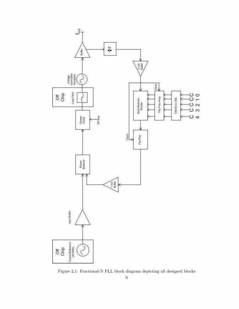
Figure 2.1: Fractional-N PLL block diagram depicting all designed blocks8
fosc =1
2π√LC
(2.1)
The relationship between tuning voltage and the output frequency of the VCO can be
calculated using (2.2). Where KV CO is the gain of the VCO which relates the frequency of
oscillation to the tuning voltage applied.
ωV CO = KV COvc (2.2)
The phase detector will output an error signal based off of the phase difference of the
reference signal and a divided down copy of the synthesized signal. The frequency of the
VCO can be converted to phase using (2.3) to help calculate the phase error.
ω =dθ
dt(2.3)
Using this relationship the phase of the VCO can be found using (2.4)
θV CO =∫ωV COdt = KV CO
∫ t
0vcτdτ (2.4)
Converting (2.4) to the frequency domain with the Laplace transform gives :
θV CO(s)vs(s)
=KV CO
s(2.5)
This results in a transfer function for the VCO and MMD found in (2.6)
θovc
=1N· KV CO
s(2.6)
9
2.1.2 Multi-Modulus Divider
The frequency divider presented in this PLL design is a five bit multi-modulus divider.
The MMD has a division ratio of 128-159, with the capability to program the MMD with
an integer step size. The MMD must be able to divide the frequency of the VCO down to
the frequency of the reference signal. The MMD presented in this paper has been optimized
for area and power consumption, and was designed using a generic algorithm to reduce the
number of division stages in the MMD.
2.1.3 Phase Frequency Detector and Charge Pump
The phase frequency detector (PFD) in the PLL acts as the summing junction for
the feedback system. The phase detector accepts inputs from a reference crystal and the
MMD output. The output of the phase detector is a waveform proportional to the phase
error between the reference signal and MMD output. The PFD outputs two signals, Up
and Down, these signals are a square wave signal that display the phase error between
the two signals. The charge pump converts the up and down signals of the PFD to a
single output current. This current will rise or fall to adjust the frequency of the oscillator
accordingly. The current in the charge pump becomes a source or sink depending on the
phase information in the up and down signal. This output current is then applied to the
loop filter [2]. The gain of the PFD when used with a charge pump can be found using
(2.7), where I is the current of the charge pump.
Kpdcp =I
2π(2.7)
2.1.4 Loop Filter
The loop filter presented in this paper is a 2nd order low pass filter. The filter converts
the output current of the charge pump to a voltage that can be applied to the tuning node
of the VCO. The admittance of the second order loop filter can be found in (2.8). The filter
can be seen in figure 7.1
10
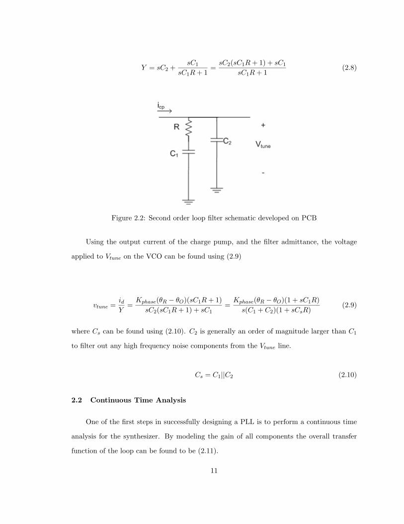
Y = sC2 +sC1
sC1R+ 1=sC2(sC1R+ 1) + sC1
sC1R+ 1(2.8)
Figure 2.2: Second order loop filter schematic developed on PCB
Using the output current of the charge pump, and the filter admittance, the voltage
applied to Vtune on the VCO can be found using (2.9)
vtune =idY
=Kphase(θR − θO)(sC1R+ 1)
sC2(sC1R+ 1) + sC1=Kphase(θR − θO)(1 + sC1R)s(C1 + C2)(1 + sCsR)
(2.9)
where Cs can be found using (2.10). C2 is generally an order of magnitude larger than C1
to filter out any high frequency noise components from the Vtune line.
Cs = C1||C2 (2.10)
2.2 Continuous Time Analysis
One of the first steps in successfully designing a PLL is to perform a continuous time
analysis for the synthesizer. By modeling the gain of all components the overall transfer
function of the loop can be found to be (2.11).
11
θoθR
=AoKphaseF (s)
N · KV COs
1 + AoKphaseF (s)N · KV CO
s
=KF (s)
s+KF (s)(2.11)
The variable K is used to represent:
K =AoKphaseKV CO
N(2.12)
For initial simplicity a transfer function will be derived for a second order system, and
then the transfer function for a third order system will be given later in this section. The
response of a first order loop filter using a single resistor and a capacitor C1 can be found
using:
F (s) = (R+1sC1
) =sC1R+ 1sC1
(2.13)
It is worth observing that the transfer function described above can be thought of as an
impedance due to the fact that the input is a current that is converted to a voltage. With
that in mind we can substitute the above equation into (2.11) to give:
θoθR
=IKV CO2π·N (R+ 1
sC1)
s+ IKV CO2π·N (R+ 1
sC1)
(2.14)
This gives a second order transfer function for the PLL with two poles and a zero.
It can be seen that the resistor (R) of the loop filter plays a very important role in the
stability of the loop. Without the resistor, the poles of the system would lay on the jω axis,
which would cause the loop to go unstable and begin oscillating. Using (2.14) the natural
frequency of the system can be determined and can be shown in equation 2.15.
ωn =√
IKV CO
2π ·NC1(2.15)
12
Additionally the damping constant for the system can be found to be:
ζ =R
2
√IKV COC1
2π ·N(2.16)
It is common to find the R and C1 for the loop filter after determining a natural
frequency and damping constant for the system. By rearranging (2.15) and ( 2.16) R and
C1 can be calculated using:
C1 =IKV CO
2π ·Nω2n
(2.17)
and
R = 2ζ√
2πNIKV COC1
= ζ4πNωnIKV CO
(2.18)
Using the natural frequency and damping constant, the transfer function of the syn-
thesizer can be simplified to the following:
θoθR
=ω2n( 2ζ
ωns+ 1)
s2 + 2ζωns+ ω2n
(2.19)
By rewriting the transfer function in terms of ωn and ζ it becomes much easier to see the
relationship between the poles and zero locations. With this in mind the transfer function
of the system can be plotted. The frequency response of the system can be seen in figure
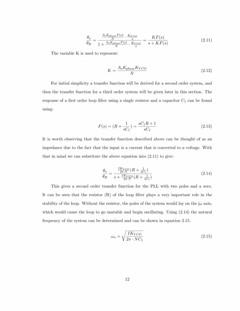
2.3. From the figure the 3dB bandwidth of the system can be determined. The bandwidth
can be calculated mathematically using:
ω3dB = ωn
√1 + 2ζ2 +
√4ζ4 + 4ζ2 + 2 (2.20)
By using capacitor C2 in the loop filter a high frequency pole is added to the transfer
function of the system. C2 is generally chosen to be roughly one-tenth the size of C1. This
13
Figure 2.3: PLL frequency response diagram generated in MATLAB
14
high frequency pole is added to help filter out some of the high frequency ripples that
sometimes are present on the VCO voltage control line. The open loop transfer function
for a third order PLL can be found to be:
θoθR
=KV COKpdcp(1 + sC1R)s2N(C1 + C2)(1 + sCsR)
(2.21)
Where Cs is the series combination of C1 and C2. It can be seen that at low frequencies
the slope of the magnitude is -40 dB/dec with 180o of phase shift. As the frequency
approaches the zero of the system the slope is reduced to -20 dB/dec, while the phase rises
to 90o. When the high frequency pole caused by C2 is reached the slope returns to -40
dB/dec and the phase returns to 180o. This shows that the optimum stability point can be
reached where the unity gain point is at the geometric mean of the zero and high frequency
pole. This is the location where the phase shift in the system will be furthest away from
180o. In order to perform a full stability analysis the closed loop poles would need to be
examined. This can be accomplished by analyzing the closed loop gain of the system as
seen in (2.22)
θoθR
=KV COKpdcp(1 + sC1R)
s2N(C1 + C2)(1 + sCsR) +KV COKpdcp(1 + sC1R)(2.22)
By analyzing the above transfer function it can be seen that if the zero and high frequency
pole are not close together, then the effects of including C2 and the high frequency are
not seen until the higher frequencies are reached. Generally the value of C2 is sized to be
roughly one-tenth the size of C1. It is worth noting however, that for relatively high values
of ζ a larger value of R will be needed. This may cause the series combination of R and C1
to be close to the impedance value of C2 at the loop bandwidth. Should this happen the
value of C2 should be reduced to a value smaller than one-tenth of C1 to ensure that the
transfer function for the system remains accurate.
15
2.3 Discrete-Time Analysis
As was seen in the previous section, there are certain instances where a continuous
time analysis is not fully accurate. In these situations, especially when the loop bandwidth
approaches the reference frequency, a more dependable analysis method is needed. For these
situations the phase frequency detector can be thought of as a sampling element, so that
the system can be treated as a discrete-time feedback system. When the system is locked
on frequency there ideally should be extremely narrow pulses at the reference frequency,
and because the charge pump can be treated as an integrator it has infinite gain at dc. So
as long as the deviation between the reference and synthesized frequency is small the phase
error will approach zero, allowing the phase detector and charge pump to act as an ideal
sampler. The loop filter can then be viewed as a hold function due to the time needed to
charge and discharge the capacitors in the filter. To fully view the PLL as a sampled system
the models for the VCO, PD, charge pump, LPF, and MMD must all be converted from
the s domain to the z domain. By ignoring C2 the open-loop transfer function can easily
be found to be:
GOL(s) = F (s) ·KpdcpKV CO
N · s·
(1− e−sT
s
)(2.23)
GOL(s) =(R+
1sC1
)·KV COKpdcp
N · s
(1− e−sT
s
)(2.24)
GOL(s) = ω2n
(2ζωns+ 1s2
)·(
1− e−sT
s
)(2.25)
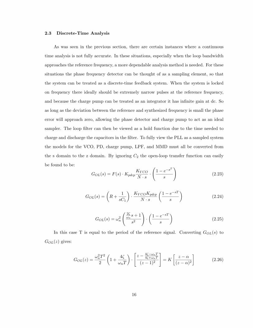
In this case T is equal to the period of the reference signal. Converting GOL(s) to
GOL(z) gives:
GOL(z) =ω2nT
2
2
(1 +
4ζωnT
)·
[z − 4ζ−ωnT
4ζ+ωnT
(z − 1)2
]= K
[z − α
(z − α)2
](2.26)
16
Where α is the open loop zero with a value between -1 and +1. The value of α is dependent
on the value of the reference signal, and can be calculated using (2.27)
α =4ζ − ωnT4ζ + ωnT
(2.27)
Also dependant on the reference signal is the open loop gain, K, which can be found by
using:
K =ω2nT
2
2
(1 +
4ζωnT
)(2.28)
With α and the open loop gain, the closed loop gain of the synthesizer can be determined
to be:
G(z) =K(z − α)
z2 + (K − 2)z + (1−)(2.29)
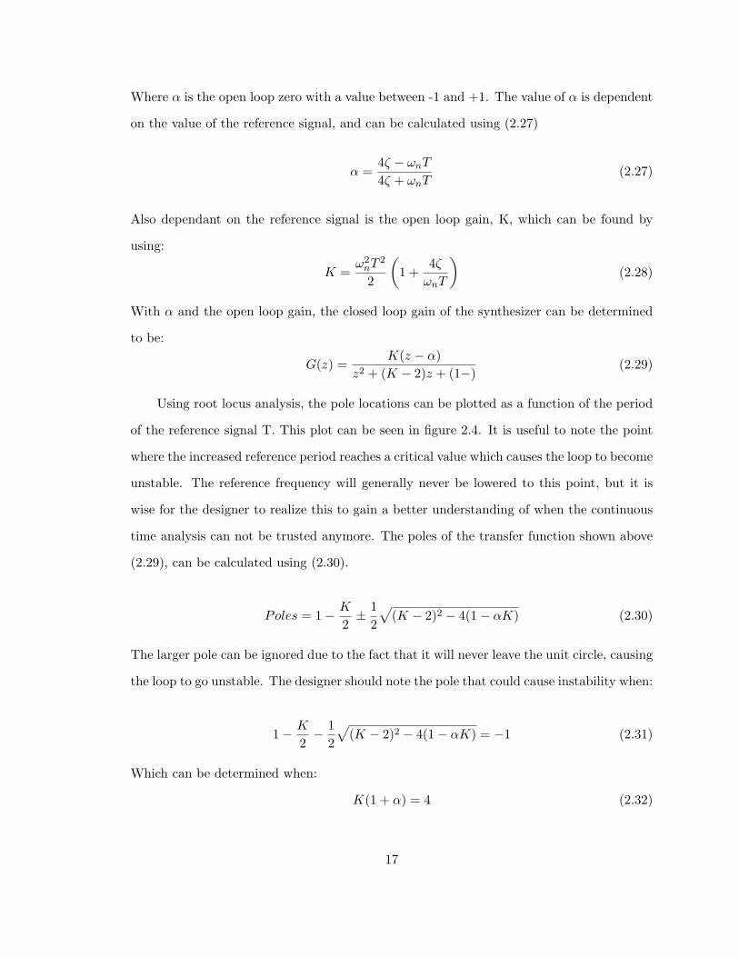
Using root locus analysis, the pole locations can be plotted as a function of the period
of the reference signal T. This plot can be seen in figure 2.4. It is useful to note the point
where the increased reference period reaches a critical value which causes the loop to become
unstable. The reference frequency will generally never be lowered to this point, but it is
wise for the designer to realize this to gain a better understanding of when the continuous
time analysis can not be trusted anymore. The poles of the transfer function shown above
(2.29), can be calculated using (2.30).
Poles = 1− K
2± 1
2
√(K − 2)2 − 4(1− αK) (2.30)
The larger pole can be ignored due to the fact that it will never leave the unit circle, causing
the loop to go unstable. The designer should note the pole that could cause instability when:
1− K
2− 1
2
√(K − 2)2 − 4(1− αK) = −1 (2.31)
Which can be determined when:
K(1 + α) = 4 (2.32)
17

Figure 2.4: PLL Root Locus Diagram
18
The critical period of the loop TUS where it will go unstable, can be determined by back
substituting K and α. That period can be found to be:
TUS =1ωnζ
=2π
ωrefcrt(2.33)
ωref crt is the reference frequency when the loop will begin to oscillate and go unstable.
ωrefctr = 2πζωn (2.34)
ωrefωn≥ 2πζ (2.35)
For example if a synthesizer was needed with a ζ=0.634 the ratio of ωref/ωn in (2.35) must
be greater than 3.98. So for a reference frequency of 30 MHz, the loop bandwidth must not
go over 7.53 MHz. Some sources say that a common ratio to use when designing your loop
bandwidth is 10:1.
2.4 Transient Analysis
Unfortunately the s and z domain equations presented in the previous two sections are
not able to fully characterize the behavior of a PLL. This is largely due to the fact that
the phase detector is not always able to track phase changes if there is an extremely large
change in the phase of the input. This is due to the fact that the phase detector has a small
range of linear operation. The tri-state phase detector used in the design of this PLL only
has a linear range of ±2π. Should an input cause the loop to experience a phase change
larger than 2π the loop will undergo a non-linear action called cycle slipping. The loop will
act to try to correct this, and lock on and track the input phase once more. This action is
referred to as acquisition mode. The PLL remains in acquisition mode until the loop locks
onto the appropriate frequency and phase. However, this event in some cases can cause the
VCO to get off frequency and phase from the reference signal in a mode outside of its linear
19
range of motion. This can cause the PLL to lose its lock indefinitely. The PLL usually
enters acquisition mode when the device is first powered on, and the loop is attempting to
gain its initial lock.
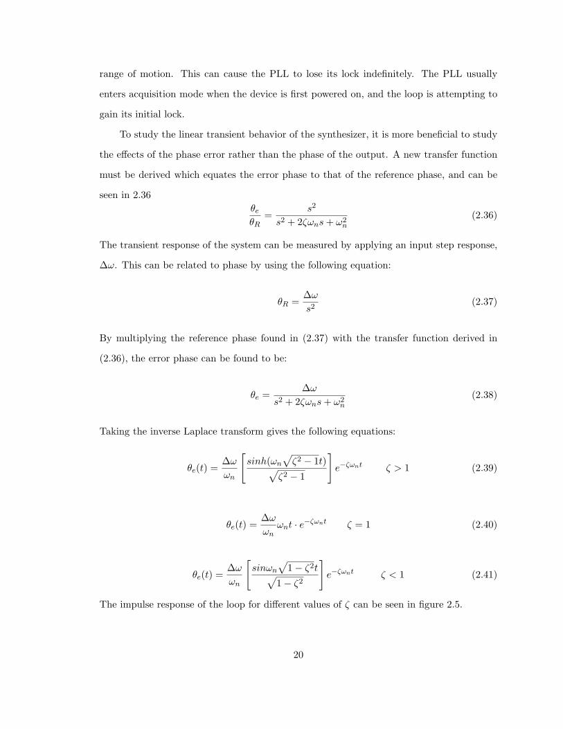
To study the linear transient behavior of the synthesizer, it is more beneficial to study
the effects of the phase error rather than the phase of the output. A new transfer function
must be derived which equates the error phase to that of the reference phase, and can be
seen in 2.36θeθR
=s2
s2 + 2ζωns+ ω2n
(2.36)
The transient response of the system can be measured by applying an input step response,
∆ω. This can be related to phase by using the following equation:
θR =∆ωs2
(2.37)
By multiplying the reference phase found in (2.37) with the transfer function derived in
(2.36), the error phase can be found to be:
θe =∆ω
s2 + 2ζωns+ ω2n
(2.38)
Taking the inverse Laplace transform gives the following equations:
θe(t) =∆ωωn
[sinh(ωn
√ζ2 − 1t)√
ζ2 − 1
]e−ζωnt ζ > 1 (2.39)
θe(t) =∆ωωn
ωnt · e−ζωnt ζ = 1 (2.40)
θe(t) =∆ωωn
[sinωn
√1− ζ2t√
1− ζ2
]e−ζωnt ζ < 1 (2.41)
The impulse response of the loop for different values of ζ can be seen in figure 2.5.
20
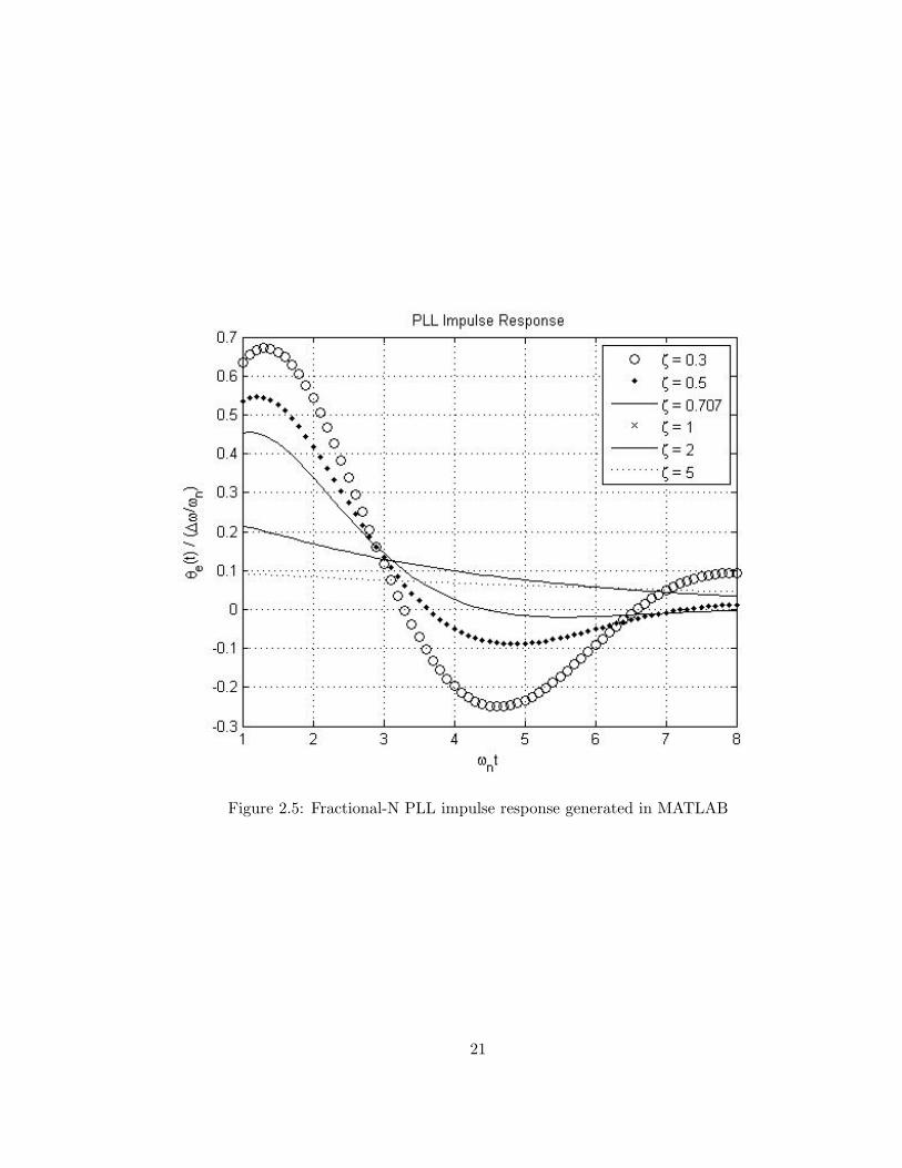
Figure 2.5: Fractional-N PLL impulse response generated in MATLAB
21
Fractional-N PLL Design
A second order fractional-N PLL was designed using a MMD, PFD, CP and loop filter.
A damping coefficient of 0.707 was chosen, and the bandwidth of the filter was chosen to
be 110 kHz. The natural frequency can be found using (2.42).
ωn =ω3dB
1 + ζ√
2= 2π · 55kHz (2.42)
The maximum applied frequency step for this PLL can be found to be:
∆ω = θe max · ωn0.46 = 751.25kHz(2.43)Figure 2.5 shows that with the chosen ζ the
system settles in approximately t=7ωn≈20.25 µs. With the chosen values of ζ, ωn, I, N,
and KV CO, R and C1 can be calculated to complete the transfer function of the designed
loop. The results can be found using (2.44) and (2.45).
C1 =I ·KV CO
2π ·Nω2n
= 5nF (2.44)
R = 2ζ√
2πNIKV COC1
= ζ4πNωnIKV CO
= 19kΩ (2.45)
2.5 Noise Sources
In systems such as a receiver, the systems noise performance is a measure of the min-
imum detectable signal. In a synthesizer the noise performance is measured based on the
phase noise in the signal, since the phase noise will determine how much jitter the output
will experience in the time domain. In a receiver the concern with noise would be the
amplitude of the output, while the synthesizer is concerned primarily with the phase of the
the output signal. The output of the synthesizer can be found to be:
22
vout(t) = Vocos[ωLOt+ ϕ(t)] (2.46)
Where ωLO is the frequency of oscillation at the desired phase, and ϕn(t) is the phase noise
present in the synthesizer. Phase noise is usually referred to in dBc/Hz. The phase noise
variations could be due either to random variations or distinct spurs in the spectrum. Spurs
are commonly caused due to techniques used in fractional-N synthesis, and due to the noise
generated by the VCO. The phase noise is generally thought of as sinusoidal, and can be
seen in the following equation:
ϕn(t) = ϕpsin(ωmt) (2.47)
Noise can be generated several different ways in electronics. One of the first possible
sources of noise comes from thermal noise, which is primarily present in resistors. Thermal
noise is due to the random electron motion, and is dependent on temperature, bandwidth,
and resistance. Active devices also add 1/f noise, or shot noise. Noise can also electromag-
netically couple into the device from nearby electronics, or from other devices on the same
die.
2.5.1 In-Band Noise
MMD Noise
The multi-modulus divider is made up of high speed switching logic circuits. The rising
and falling edge of the clock can be superimposed with spurious signals and can cause a
certain amount of phase noise. This phase noise is in the frequency domain which can be
translated to phase jitter in the time domain. Kroupa performed a lot of research to derive
a formula to describe the phase noise added by a frequency divider [7][8], and can be seen
in (2.48).
ϕ2MMD(∆ω) =
10−14±1 + 10−27±1ω2do
2π∆ω2+ 10−16±1 +
10−22±1ωdo2π
(2.48)
23
Where ωdo is the frequency of the output of the divider, and ∆ω is the offset frequency.
The first term is dominated by the flicker noise, the second term is the thermal noise floor,
and the third term represents the jitter due to coupling and power supply variations.
Phase Detector Noise
Phase detectors generate flicker and thermal noise. At large phase offsets, the noise
produced by the phase detector is dominated by the thermal noise and is approximately
-160 dBc/Hz. [8] found the noise of a phase detector to be:
ϕ2PD(∆ω) =
2π · 10−14±1
∆ω2+ 10−16±1 (2.49)
Crystal Reference Noise
Crystal oscillators are very popular in PLL design due to their compact nature, low
cost, stability, and high Q. In [13] Leeson’s formula was used to derive the noise PSD of a
crystal which can be found in (2.50). In this equation ωo is the oscillation frequency of the
crystal, and ∆ωc is the corner frequency between the 1/f and thermal noise. The crystal
only adds noise very close in, but as the frequency deviation is increased the noise level
drops sharply off near ωc.
ϕ2CRY S(∆ω) = 10−16±1 ·
[1 +
(ωo
2∆ωQL
)2](
1 +ωc∆ω
)(2.50)
Loop Filter Noise
The only noise contributed by the loop filter is due to thermal noise contributed by
the resistor. This is one major reason why the loop filter is seldom larger than a second
order filter. This is to help reduce the amount of noise being directly introduced on the
VCO tuning line. The thermal noise added by the resistor is a function of the temperature,
the resistance value, and Boltzmann’s constant. The thermal noise can be found by using
(2.52). Examining the frequency response of the noise signal yields (2.53). It can be seen
24
from the frequency response that the loop filter will act as a high pass filter for the noise.
vn =√
4kTR∆f (2.51)
in =1R· vns
s+ C1+C2C1C2R
≈ 1R
vns
s+ 1C2R
(2.52)
inLPF (∆ω) =1R· vns
s+ C1+C2C1C2R
≈ 1R· vns
s+ 1C2R
(2.53)
Charge Pump Noise
It is easiest to model the output noise of the charge pump as a current, due to the fact
that the output of the charge pump is already a current. The presence of noise in the charge
pump is tied to the output pulses, so to reduce noise the loop should remain locked at all
times to reduce output pulses. Often times the noise generated by the charge pump can
become a dominant factor in the loop behavior. The two main sources of noise in the charge
pump are drain noise and flicker noise. The drain noise can be calculated using the following:
idn = 4kT(
23
)gm = 4kT
(23
)√2ox
(W
L
)IDS (2.54)
This shows that to have a low thermal noise the transistors need to have a low gm. To
achieve this the gate width should be as small as possible, while still increasing the channel
length.
This leaves 1/f noise as the only other dominant noise source in the circuit. The 1/f
noise is primarily inversely proportional to the frequency, which is why the 1/f noise be-
comes less dominant at higher frequencies. The gate referred 1/f noise can be given by:
v2ng = (f) =
K
WLCoxfα(2.55)
25
Where α is approximately one and K is a constant that comes from the process. By refer-
ring the noise from the gate to the output (eq:cp1fnoise) can be rewritten as:
i2ng = (f) =K
WLCoxfg2m =
K
WLCoxf2µCox
(W
L
)IDS =
2KµL2f
IDS (2.56)
It can be seen from (2.56) that the 1/f noise is proportional to the bias current of each
current mirror. Combining (2.54) and (2.56) will give the total noise generated by each
current mirror, and can be found by using (2.57)
i2no(f) =2KµL2f
IDS + 4kT(
23
)√2µCox
(W
L
)IDS (2.57)
With this in mind it can be found that the noise due to both current mirrors is:
i2bothmirrors(f) = 2i2no(f)tCPT0
(2.58)
By dividing the noise of the charge pump by the gain of the PD/CP stage, the phase noise
can be found to be:
θn(f) =
√i2bothmirrors
Kphase= 2π
√√√√[ 2kµL2fIDS
+ 4kT(
23
)√2µCoxI3DS
](tCPT0
)(2.59)
It can now be seen from (2.59) that the total phase noise of the charge pump is reduced by
increasing the value of the charge pump current.
26

2.5.2 Out-of-Band Noise
VCO Noise
In [6] Leeson derived the noise due to an oscillator to be :
PN =[
ωo2Q∆ω
]2(FkT2PS
)(1 +
ωc∆ω
). (2.60)
In this case C is a constant of proportionality, and ∆ω is the offset from the carrier signal.
The noise of the VCO will decay at -20 dBc/dec until the thermal noise floor has reached,
at this point the thermal noise becomes dominant. Much of the noise generated by the
VCO is only dominant outside of the loop bandwidth and has less of an effect unless a low
offset frequency is used.
2.5.3 Total System Noise
The transfer function for the noise can be easily derived. To aid in simplicity, the noise
transfer function is split into two separate transfer functions. The first transfer function,
(2.61), deals with all noise except that from the VCO. By inserting the terms for the phase
detector, charge pump, divider, crystal and loop filter (2.61) becomes (2.62).
ϕnoiseout(s)ϕnoiseI(s)
=F (s)KV COKphase
s+ F (s)KV COKphase
N
(2.61)
ϕnoiseout(s)ϕnoiseI(s)
=IKV CO2π·C1
(1 +RC1s)
s2 + R · s+ IKV CO2π·NC1
(2.62)
From (2.62) it can be seen that the in-band noise has a low-pass effect on the noise. It
can be seen that at low offset frequencies the s2 and s terms in (2.62) are negligible, and
the phase noise is dominated by the division ratio of the MMD. It is for this reason that a
fractional-N PLL is more desirable to have better control over the noise generated by the
divider.
27
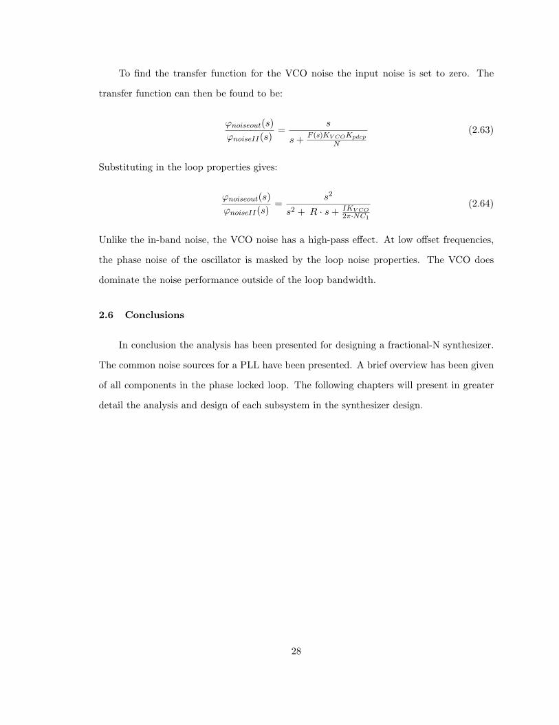
To find the transfer function for the VCO noise the input noise is set to zero. The
transfer function can then be found to be:
ϕnoiseout(s)ϕnoiseII(s)
=s
s+ F (s)KV COKpdcp
N
(2.63)
Substituting in the loop properties gives:
ϕnoiseout(s)ϕnoiseII(s)
=s2
s2 + R · s+ IKV CO2π·NC1
(2.64)
Unlike the in-band noise, the VCO noise has a high-pass effect. At low offset frequencies,
the phase noise of the oscillator is masked by the loop noise properties. The VCO does
dominate the noise performance outside of the loop bandwidth.
2.6 Conclusions
In conclusion the analysis has been presented for designing a fractional-N synthesizer.
The common noise sources for a PLL have been presented. A brief overview has been given
of all components in the phase locked loop. The following chapters will present in greater
detail the analysis and design of each subsystem in the synthesizer design.
28
Chapter 3
Logic Design for Low Voltage High Frequency Applications
Many of the building blocks in the synthesizer, such as the divider and the phase
detector, require digital logic elements. This chapter will present two of the more common
types of logic gates, complementary metal oxide semiconductor(CMOS)logic and current
mode logic (CML). The benefits of both will be presented along with why CML was chosen
for this synthesizer design.
CMOS rail to rail logic design is one of the oldest types of logic gate design. CMOS
gates only consume current when the device is changing state, so there is no constant current
drain. However, as the frequency of operation increases the amount of current consumed
by CMOS gates quickly increases. CML is not as convenient at lower frequencies due to
the constant current that is being consumed. CMOS greatly simplifies creating complex
logic functions, but requires a larger supply voltage that may not be available in many
applications.
Bipolar CML does offer much better noise performance over CMOS design in addition
to having a superior power supply rejection and the highest maximum speed. The noise
performance of the CML gate becomes very important when trying to eliminate in-band
noise sources. The better noise performance of CML is due to the fact that there is a
constant current consumption with CML, so there is no noise contributed by switching the
transistors on and off like there is in CMOS[4][24].
3.1 CMOS
CMOS logic generally produces an output signal that swings from the positive to the
negative power supply, and in high speed applications such as synthesizer design this is not
29
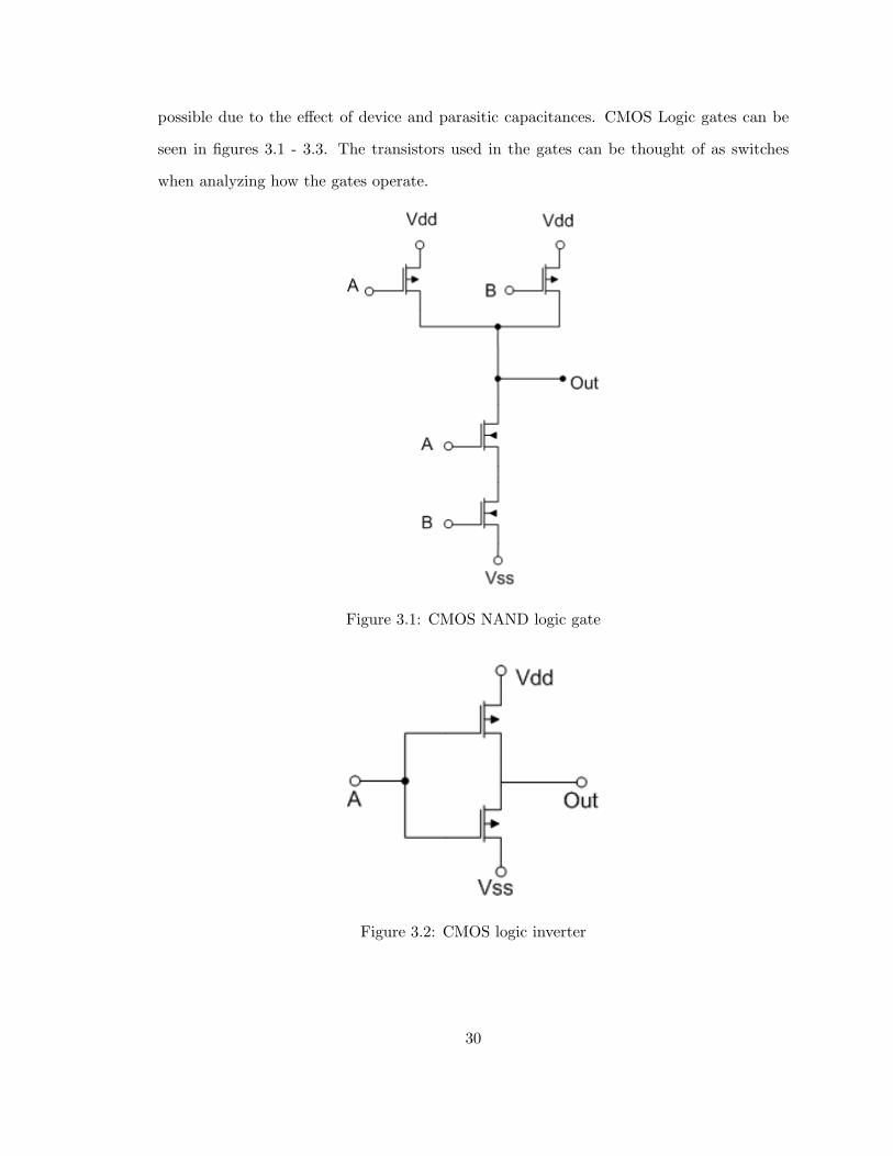
possible due to the effect of device and parasitic capacitances. CMOS Logic gates can be
seen in figures 3.1 - 3.3. The transistors used in the gates can be thought of as switches
when analyzing how the gates operate.
Figure 3.1: CMOS NAND logic gate
Figure 3.2: CMOS logic inverter
30
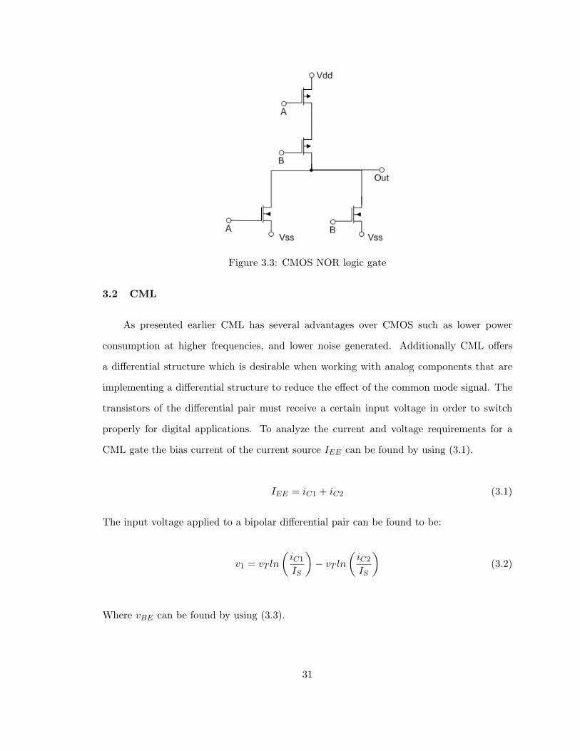
Figure 3.3: CMOS NOR logic gate
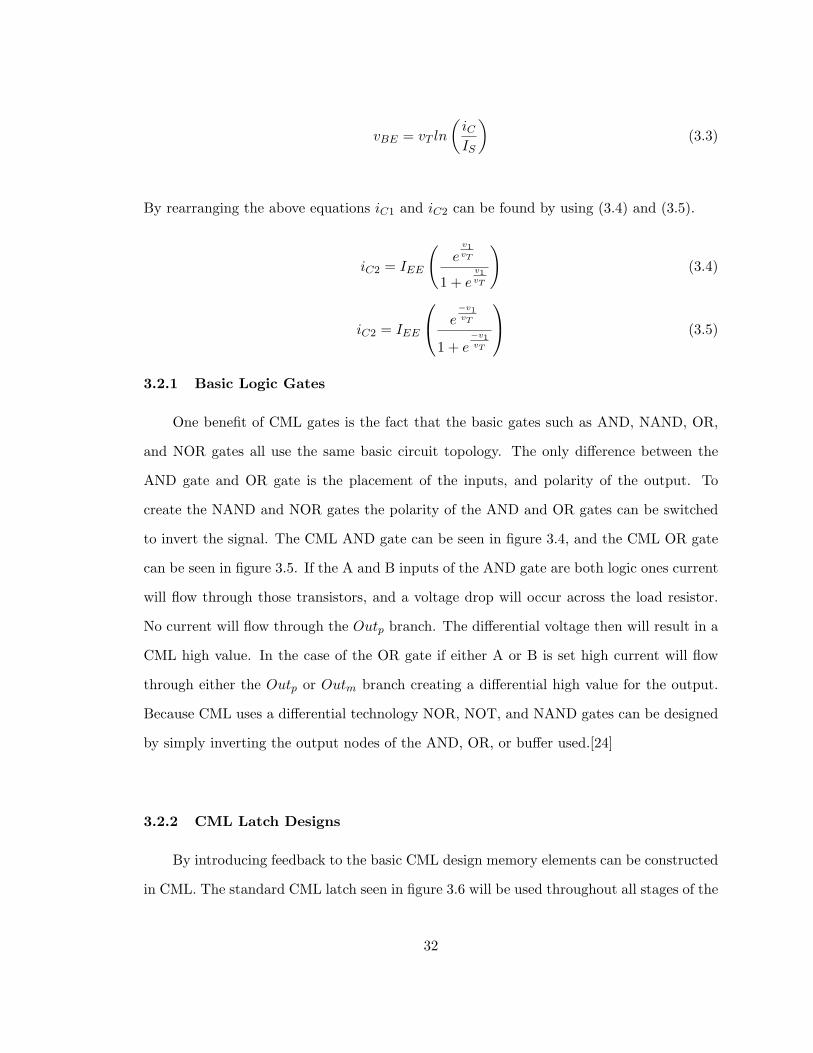
3.2 CML
As presented earlier CML has several advantages over CMOS such as lower power
consumption at higher frequencies, and lower noise generated. Additionally CML offers
a differential structure which is desirable when working with analog components that are
implementing a differential structure to reduce the effect of the common mode signal. The
transistors of the differential pair must receive a certain input voltage in order to switch
properly for digital applications. To analyze the current and voltage requirements for a
CML gate the bias current of the current source IEE can be found by using (3.1).
IEE = iC1 + iC2 (3.1)
The input voltage applied to a bipolar differential pair can be found to be:
v1 = vT ln
(iC1
IS
)− vT ln
(iC2
IS
)(3.2)
Where vBE can be found by using (3.3).
31
vBE = vT ln
(iCIS
)(3.3)
By rearranging the above equations iC1 and iC2 can be found by using (3.4) and (3.5).
iC2 = IEE
(e
v1vT
1 + ev1vT
)(3.4)
iC2 = IEE
e−v1vT
1 + e−v1vT
(3.5)
3.2.1 Basic Logic Gates
One benefit of CML gates is the fact that the basic gates such as AND, NAND, OR,
and NOR gates all use the same basic circuit topology. The only difference between the
AND gate and OR gate is the placement of the inputs, and polarity of the output. To
create the NAND and NOR gates the polarity of the AND and OR gates can be switched
to invert the signal. The CML AND gate can be seen in figure 3.4, and the CML OR gate
can be seen in figure 3.5. If the A and B inputs of the AND gate are both logic ones current
will flow through those transistors, and a voltage drop will occur across the load resistor.
No current will flow through the Outp branch. The differential voltage then will result in a
CML high value. In the case of the OR gate if either A or B is set high current will flow
through either the Outp or Outm branch creating a differential high value for the output.
Because CML uses a differential technology NOR, NOT, and NAND gates can be designed
by simply inverting the output nodes of the AND, OR, or buffer used.[24]
3.2.2 CML Latch Designs
By introducing feedback to the basic CML design memory elements can be constructed
in CML. The standard CML latch seen in figure 3.6 will be used throughout all stages of the
32
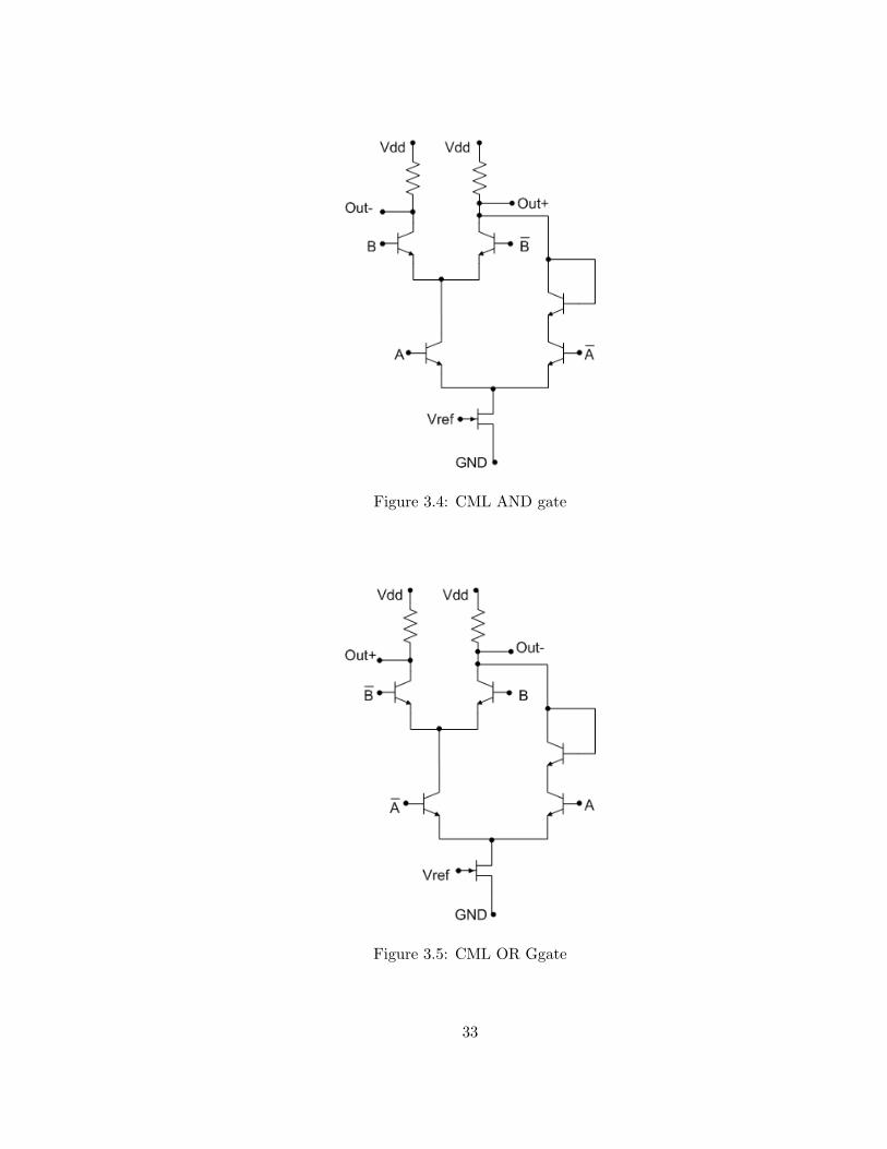
Figure 3.4: CML AND gate
Figure 3.5: CML OR Ggate
33
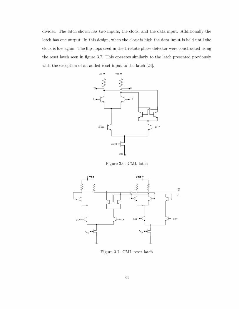
divider. The latch shown has two inputs, the clock, and the data input. Additionally the
latch has one output. In this design, when the clock is high the data input is held until the
clock is low again. The flip-flops used in the tri-state phase detector were constructed using
the reset latch seen in figure 3.7. This operates similarly to the latch presented previously
with the exception of an added reset input to the latch [24].
Figure 3.6: CML latch
Figure 3.7: CML reset latch
34
3.2.3 CML Support Circuitry
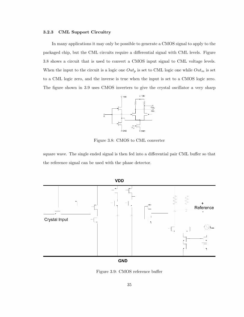
In many applications it may only be possible to generate a CMOS signal to apply to the
packaged chip, but the CML circuits require a differential signal with CML levels. Figure
3.8 shows a circuit that is used to convert a CMOS input signal to CML voltage levels.
When the input to the circuit is a logic one Outp is set to CML logic one while Outm is set
to a CML logic zero, and the inverse is true when the input is set to a CMOS logic zero.
The figure shown in 3.9 uses CMOS inverters to give the crystal oscillator a very sharp
Figure 3.8: CMOS to CML converter
square wave. The single ended signal is then fed into a differential pair CML buffer so that
the reference signal can be used with the phase detector.
Figure 3.9: CMOS reference buffer
35
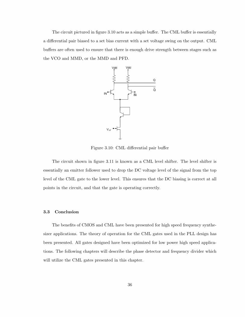
The circuit pictured in figure 3.10 acts as a simple buffer. The CML buffer is essentially
a differential pair biased to a set bias current with a set voltage swing on the output. CML
buffers are often used to ensure that there is enough drive strength between stages such as
the VCO and MMD, or the MMD and PFD.
Figure 3.10: CML differential pair buffer
The circuit shown in figure 3.11 is known as a CML level shifter. The level shifter is
essentially an emitter follower used to drop the DC voltage level of the signal from the top
level of the CML gate to the lower level. This ensures that the DC biasing is correct at all
points in the circuit, and that the gate is operating correctly.
3.3 Conclusion
The benefits of CMOS and CML have been presented for high speed frequency synthe-
sizer applications. The theory of operation for the CML gates used in the PLL design has
been presented. All gates designed have been optimized for low power high speed applica-
tions. The following chapters will describe the phase detector and frequency divider which
will utilize the CML gates presented in this chapter.
36
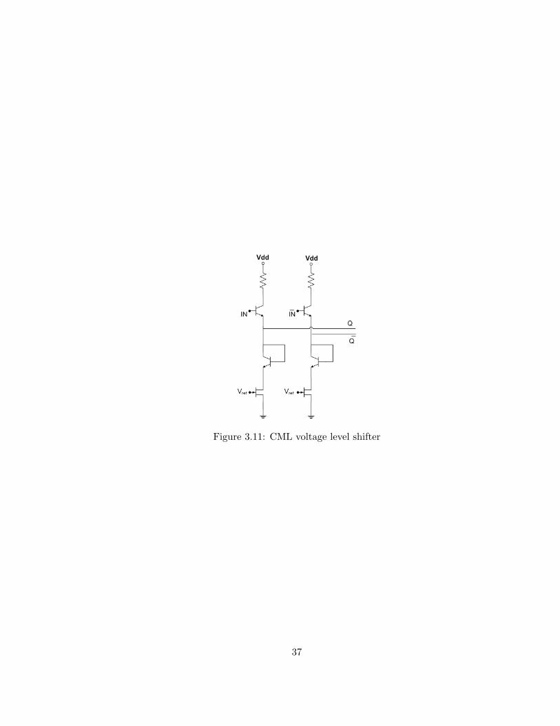
Figure 3.11: CML voltage level shifter
37
Chapter 4
Phase Detector
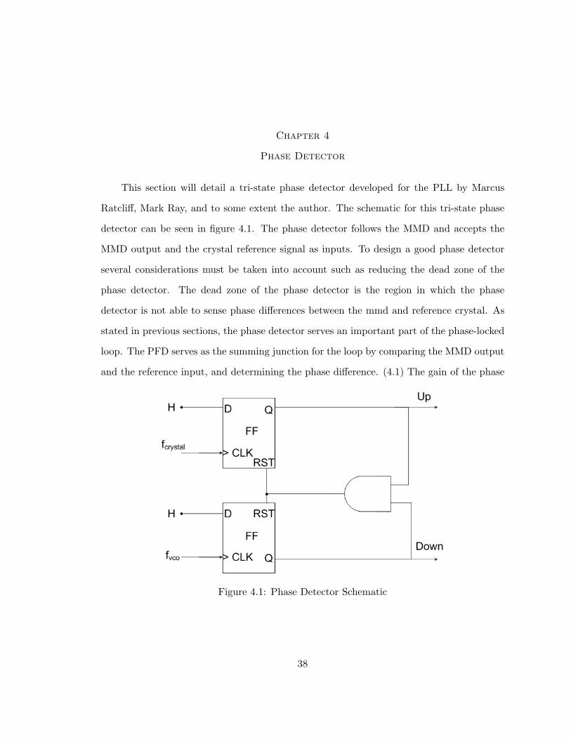
This section will detail a tri-state phase detector developed for the PLL by Marcus
Ratcliff, Mark Ray, and to some extent the author. The schematic for this tri-state phase
detector can be seen in figure 4.1. The phase detector follows the MMD and accepts the
MMD output and the crystal reference signal as inputs. To design a good phase detector
several considerations must be taken into account such as reducing the dead zone of the
phase detector. The dead zone of the phase detector is the region in which the phase
detector is not able to sense phase differences between the mmd and reference crystal. As
stated in previous sections, the phase detector serves an important part of the phase-locked
loop. The PFD serves as the summing junction for the loop by comparing the MMD output
and the reference input, and determining the phase difference. (4.1) The gain of the phase
Figure 4.1: Phase Detector Schematic
38
detector used with a charge pump can be found by using:
Kpdcp =I
2π. (4.1)
Where I is the DC magnitude of the current of the charge pump. The phase detector
will enter the cycle slipping mode if the difference in the phase between the reference signal
and the MMD output are more than 2π out of phase. In this case it is often assumed that
the MMD output and reference signal are different frequencies. At this point the phase
detector acts as a frequency detector to return the VCO back to the correct frequency.
Dead Zone in Phase Detectors
The rise and fall times in the logic gates that form the phase detector increase the
difficulty of producing short pulses. The charge pump will generally have a hard time
detecting pulses from the phase detector that are smaller than the rise time of the gates.
With this in mind, it is critical to the phase detector design to make sure that rise time is
optimized for each cell, and that the layout of the circuit has a minimal effect. The dead
zone of the phase detector can be calculated by using (4.2).
Dead zone edge = ±τπT
(4.2)
Where τ is the rise time, and T is the period of the reference signal. Much work has been
done in [22] and [23] to reduce or remove the dead zone.
4.1 Circuit Implementation
This tri-state phase detector uses low power CML logic gates as discussed in Chapter
3. The circuit implementation of the PFD can be seen in Figure 4.1. The schematic used
is one of the simplest configurations for a tri-state phase detector. The circuit consists of
two resettable flip-flops and an AND gate. There are also CML level shifters not pictured
39
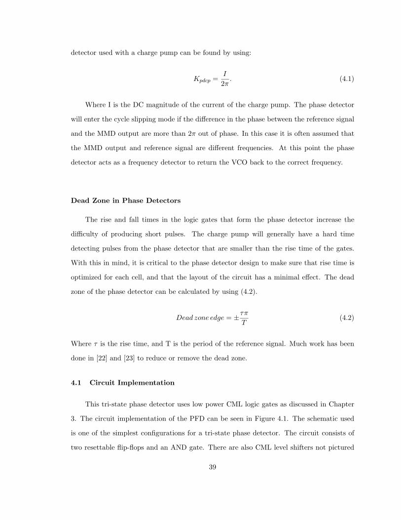
to ensure that the DC biasing is correct at all points in the circuit. The flip-flops were
constructed using two reset CML D-latch circuits discussed in Chapter 3. The schematic
for the reset flip-flop can be seen in Figure 4.2. In this diagram H is constantly set to a
logic 1. The MMD and reference signals act as the clock inputs to the flip-flops. When
either input signal reaches a logic one, the output of the corresponding flip-flop is set to
high. When both signals are high, the AND gate produces a high pulse that is applied
to the reset terminal on the flip-flops causing the system to reset.When the phase of the
reference signal is leading the divider signal of the corresponding flip-flop will remain high,
and when the divider leads the reference signal the corresponding flip-flop will produce a
high pulse equal the phase difference. When the output of both flip flops are high the AND
gate resets the system. When the system is locked there will be instantaneous pulses at the
falling edge of the clock, and the charge pump will hold the necessary charge.
Figure 4.2: Reset Flip Flop
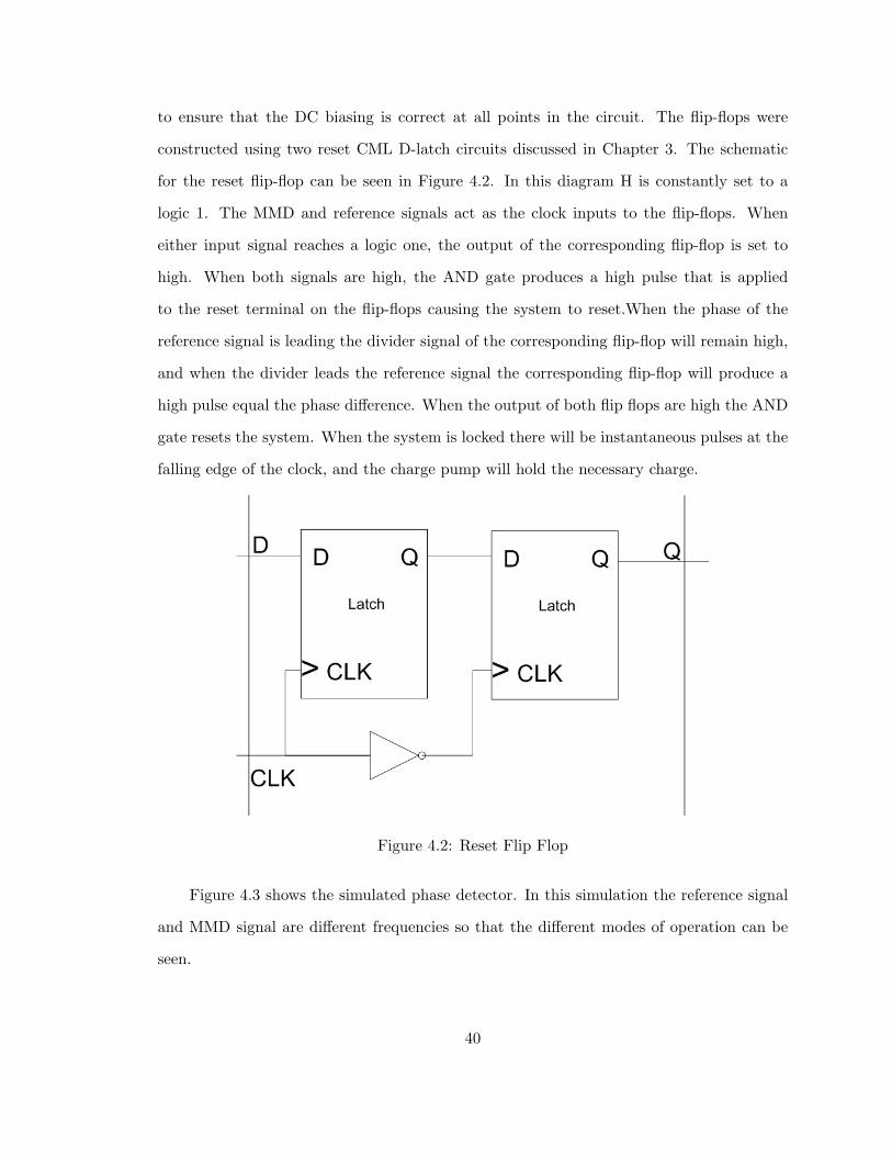
Figure 4.3 shows the simulated phase detector. In this simulation the reference signal
and MMD signal are different frequencies so that the different modes of operation can be
seen.
40
Figure 4.3: Cadence Phase Detector Simulation
4.2 Conclusion
A simple tri-state phase frequency detector has been presented. Issues in phase detector
design such as the dead zone, and matching have been presented. This phase detector will
directly drive the charge pump which will be described in a later chapter.
41
Chapter 5
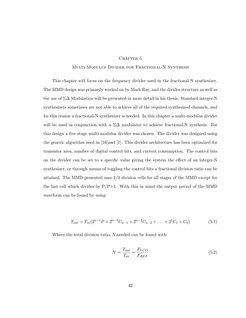
Multi-Modulus Divider for Fractional-N Synthesis
This chapter will focus on the frequency divider used in the fractional-N synthesizer.
The MMD design was primarily worked on by Mark Ray, and the divider structure as well as
the use of Σ∆ Modulation will be presented in more detail in his thesis. Standard integer-N
synthesizers sometimes are not able to achieve all of the required synthesized channels, and
for this reason a fractional-N synthesizer is needed. In this chapter a multi-modulus divider
will be used in conjunction with a Σ∆ modulator to achieve fractional-N synthesis. For
this design a five stage multi-modulus divider was chosen. The divider was designed using
the generic algorithm used in [16]and [1]. This divider architecture has been optimized for
transistor area, number of digital control bits, and current consumption. The control bits
on the divider can be set to a specific value giving the system the effect of an integer-N
synthesizer, or through means of toggling the control bits a fractional division ratio can be
attained. The MMD presented uses 2/3 division cells for all stages of the MMD except for
the last cell which divides by P/P+1. With this in mind the output period of the MMD
waveform can be found by using:
Tout = Tin(2n−1P + 2n−1Cn−1 + 2n−2Cn−2 + . . . + 21C1 + C0) (5.1)
Where the total division ratio, N,needed can be found with:
N =ToutTin
=FV COFREF
(5.2)
42
5.1 Generic MMD Design Algorithm
The structure presented in [17] uses cascaded cells that can divide the frequency by two
or three. The generic algorithm presented in [16] and [1]can be used to generate a MMD
that uses the fewest number of divide by 2/3 cells, and a P/P+1 cell at the end to achieve
the desired range of division ratios. This algorithm can greatly reduce the die area of the
MMD by reducing the number of stages needed. By keeping all stages, with the exception
of the last stage, of the MMD as divide by 2/3 cells a unit step increment in tuning range
can be achieved. The algorithm consists of the following steps:
1. Assume that the required division ratio is from Dmin to Dmax; the division ratio range
is (Dmax −Dmin + 1)
2. If the required range is greater than the minimum division ratio, Dmin the MMD is
referred to the architecture in [17].
3. The implemented MMD range, defined from M to N can be larger than the required
range. Initially set M=Dmin.
4. Now the number of cells required becomes N=dlog2(Dmax −M + 1)e. Where function
dae denotes rounding a to the nearest integer towards plus infinity.
5. The division ratio for the last cell can be found from P =⌊M/2n−1
⌋. Where bac
denotes rounding a to the nearest integer towards zero.
6. If M/2n−1 is not an integer, then reset M=P·2n−1 and go to step four.
7. If M/2n−1 is an integer, we have to decide recursively whether using a single P/P+1
cell or using a combination of a 2/3 cell and a bP/2cbP/2c+1 will achieve lower current
consumption and smaller die size.
8. The final MMD architecture is thus a combination of stages with:
(2/3)1 →(2/3)2 → · · · →(2/3)n−1 →(P/P+1)n
43
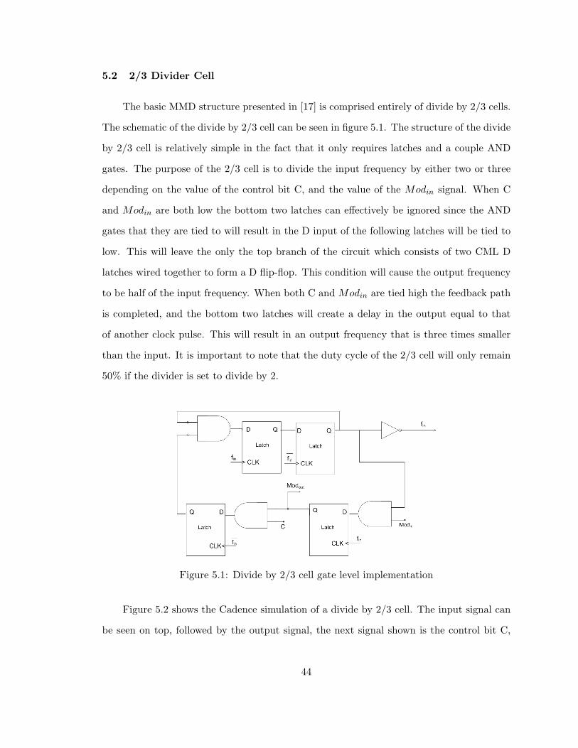
5.2 2/3 Divider Cell
The basic MMD structure presented in [17] is comprised entirely of divide by 2/3 cells.
The schematic of the divide by 2/3 cell can be seen in figure 5.1. The structure of the divide
by 2/3 cell is relatively simple in the fact that it only requires latches and a couple AND
gates. The purpose of the 2/3 cell is to divide the input frequency by either two or three
depending on the value of the control bit C, and the value of the Modin signal. When C
and Modin are both low the bottom two latches can effectively be ignored since the AND
gates that they are tied to will result in the D input of the following latches will be tied to
low. This will leave the only the top branch of the circuit which consists of two CML D
latches wired together to form a D flip-flop. This condition will cause the output frequency
to be half of the input frequency. When both C and Modin are tied high the feedback path
is completed, and the bottom two latches will create a delay in the output equal to that
of another clock pulse. This will result in an output frequency that is three times smaller
than the input. It is important to note that the duty cycle of the 2/3 cell will only remain
50% if the divider is set to divide by 2.
Figure 5.1: Divide by 2/3 cell gate level implementation
Figure 5.2 shows the Cadence simulation of a divide by 2/3 cell. The input signal can
be seen on top, followed by the output signal, the next signal shown is the control bit C,
44
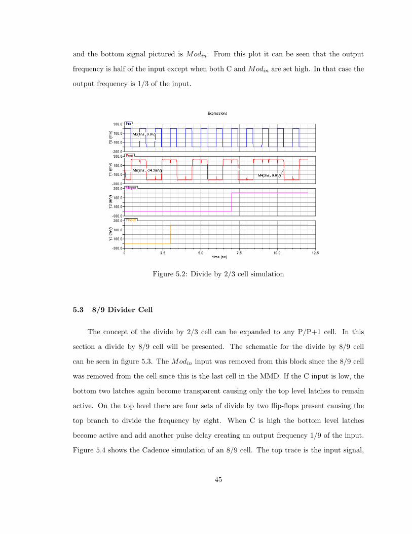
and the bottom signal pictured is Modin. From this plot it can be seen that the output
frequency is half of the input except when both C and Modin are set high. In that case the
output frequency is 1/3 of the input.
Figure 5.2: Divide by 2/3 cell simulation
5.3 8/9 Divider Cell
The concept of the divide by 2/3 cell can be expanded to any P/P+1 cell. In this
section a divide by 8/9 cell will be presented. The schematic for the divide by 8/9 cell
can be seen in figure 5.3. The Modin input was removed from this block since the 8/9 cell
was removed from the cell since this is the last cell in the MMD. If the C input is low, the
bottom two latches again become transparent causing only the top level latches to remain
active. On the top level there are four sets of divide by two flip-flops present causing the
top branch to divide the frequency by eight. When C is high the bottom level latches
become active and add another pulse delay creating an output frequency 1/9 of the input.
Figure 5.4 shows the Cadence simulation of an 8/9 cell. The top trace is the input signal,
45
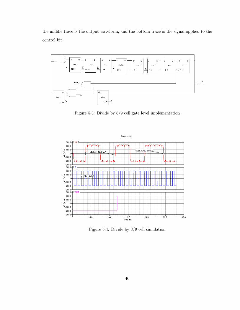
the middle trace is the output waveform, and the bottom trace is the signal applied to the
control bit.
Figure 5.3: Divide by 8/9 cell gate level implementation
Figure 5.4: Divide by 8/9 cell simulation
46
5.4 Multi-Modulus Divider Architecture
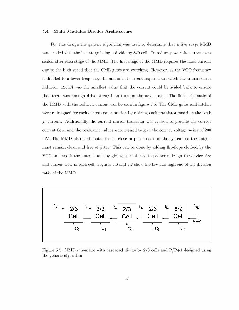
For this design the generic algorithm was used to determine that a five stage MMD
was needed with the last stage being a divide by 8/9 cell. To reduce power the current was
scaled after each stage of the MMD. The first stage of the MMD requires the most current
due to the high speed that the CML gates are switching. However, as the VCO frequency
is divided to a lower frequency the amount of current required to switch the transistors is
reduced. 125µA was the smallest value that the current could be scaled back to ensure
that there was enough drive strength to turn on the next stage. The final schematic of
the MMD with the reduced current can be seen in figure 5.5. The CML gates and latches
were redesigned for each current consumption by resizing each transistor based on the peak
ft current. Additionally the current mirror transistor was resized to provide the correct
current flow, and the resistance values were resized to give the correct voltage swing of 200
mV. The MMD also contributes to the close in phase noise of the system, so the output
must remain clean and free of jitter. This can be done by adding flip-flops clocked by the
VCO to smooth the output, and by giving special care to properly design the device size
and current flow in each cell. Figures 5.6 and 5.7 show the low and high end of the division
ratio of the MMD.
Figure 5.5: MMD schematic with cascaded divide by 2/3 cells and P/P+1 designed usingthe generic algorithm
47
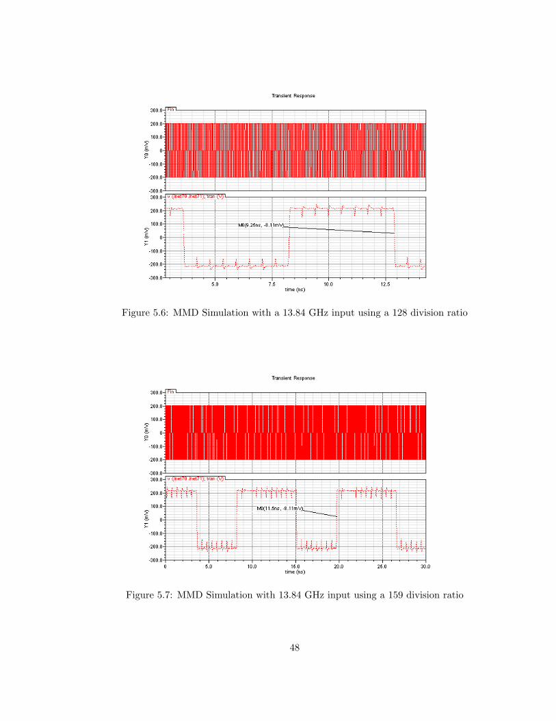
Figure 5.6: MMD Simulation with a 13.84 GHz input using a 128 division ratio
Figure 5.7: MMD Simulation with 13.84 GHz input using a 159 division ratio
48
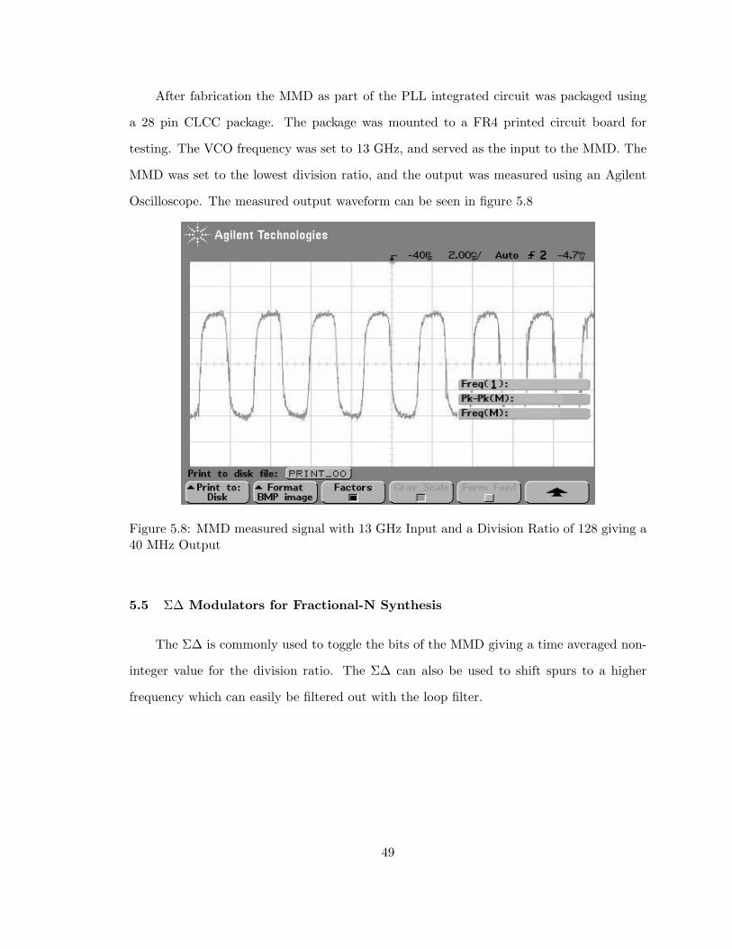
After fabrication the MMD as part of the PLL integrated circuit was packaged using
a 28 pin CLCC package. The package was mounted to a FR4 printed circuit board for
testing. The VCO frequency was set to 13 GHz, and served as the input to the MMD. The
MMD was set to the lowest division ratio, and the output was measured using an Agilent
Oscilloscope. The measured output waveform can be seen in figure 5.8
Figure 5.8: MMD measured signal with 13 GHz Input and a Division Ratio of 128 giving a40 MHz Output
5.5 Σ∆ Modulators for Fractional-N Synthesis
The Σ∆ is commonly used to toggle the bits of the MMD giving a time averaged non-
integer value for the division ratio. The Σ∆ can also be used to shift spurs to a higher
frequency which can easily be filtered out with the loop filter.
49
5.6 Conclusion
A generic algorithm has been presented for designing a modular frequency divider with
an inter step size in the division ratio. The divider has been optimized for low power high
speed applications.
50
Chapter 6
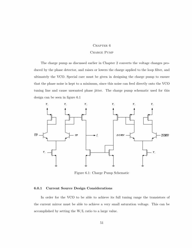
Charge Pump
The charge pump as discussed earlier in Chapter 2 converts the voltage changes pro-
duced by the phase detector, and raises or lowers the charge applied to the loop filter, and
ultimately the VCO. Special care must be given in designing the charge pump to ensure
that the phase noise is kept to a minimum, since this noise can feed directly onto the VCO
tuning line and cause unwanted phase jitter. The charge pump schematic used for this
design can be seen in figure 6.1
Figure 6.1: Charge Pump Schematic
6.0.1 Current Source Design Considerations
In order for the VCO to be able to achieve its full tuning range the transistors of
the current mirror must be able to achieve a very small saturation voltage. This can be
accomplished by setting the W/L ratio to a large value.
51
Another concern when designing the current source for a charge pump is creating the
best possible output resistance. Bipolar transistors could be used for their better output
impedance, but the technology used for this project does not provide PNP transistors.
Another method to improve the output impedance of a CMOS current source would be to
add degeneration resistors. These resistors, like bipolar transistors, would take away much
of the valuable voltage headroom available. Due to the low saturation voltage of MOS
transistors a cascode transistor could be added to increase the output resistance without
taking away too much of the available voltage headroom.
6.0.2 Reference Feed-through
In certain cases when the loop is locked and the currents coming from the UP and
DOWN branches are mismatched, the charge pump will place an unnecessary amount of
charge on the loop filter. This will cause the PD/CP to act to fix this error on the next
clock cycle. This unnecessary pulse will be applied to the VCO and will appear as an AC
signal at the reference frequency. This will cause the VCO signal to be modulated by the
reference feedthrough.
6.1 Charge Pump Circuit Implementation
The charge pump presented in this chapter is well suited to the differential nature of
the phase detector outputs. The UP and DOWN inputs on the charge pump are a bipolar
differential pair. The signal from up and down branch are mirrored to the output stage
of the charge pump. The current flowing through the current mirror will act as a current
source adding charge to the output, while the DOWN signal will act as a current sink and
will absorb some of the charge present on the output. While this schematic allows the charge
pump to be used with the CML logic gates presented earlier, this charge pump design is
not as efficient as other alternatives due to the constant bias current due to the differential
pairs. CML does provide better current matching than a traditional CMOS charge pump.
The charge pump presented in this thesis is a BiCMOS design in order to take advantage
52
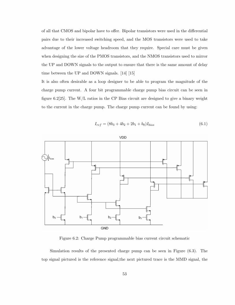
of all that CMOS and bipolar have to offer. Bipolar transistors were used in the differential
pairs due to their increased switching speed, and the MOS transistors were used to take
advantage of the lower voltage headroom that they require. Special care must be given
when designing the size of the PMOS transistors, and the NMOS transistors used to mirror
the UP and DOWN signals to the output to ensure that there is the same amount of delay
time between the UP and DOWN signals. [14] [15]
It is also often desirable as a loop designer to be able to program the magnitude of the
charge pump current. A four bit programmable charge pump bias circuit can be seen in
figure 6.2[25]. The W/L ratios in the CP Bias circuit are designed to give a binary weight
to the current in the charge pump. The charge pump current can be found by using:
Iref = (8b3 + 4b2 + 2b1 + b0)Ibias (6.1)
Figure 6.2: Charge Pump programmable bias current circuit schematic
Simulation results of the presented charge pump can be seen in Figure (6.3). The
top signal pictured is the reference signal,the next pictured trace is the MMD signal, the
53
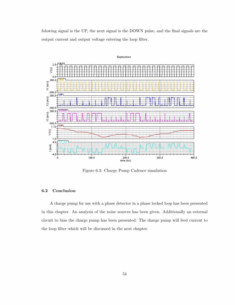
folowing signal is the UP, the next signal is the DOWN pulse, and the final signals are the
output current and output voltage entering the loop filter.
Figure 6.3: Charge Pump Cadence simulation
6.2 Conclusion
A charge pump for use with a phase detector in a phase locked loop has been presented
in this chapter. An analysis of the noise sources has been given. Additionally an external
circuit to bias the charge pump has been presented. The charge pump will feed current to
the loop filter which will be discussed in the next chapter.
54
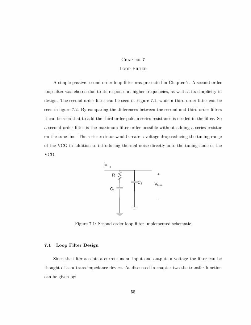
Chapter 7
Loop Filter
A simple passive second order loop filter was presented in Chapter 2. A second order
loop filter was chosen due to its response at higher frequencies, as well as its simplicity in
design. The second order filter can be seen in Figure 7.1, while a third order filter can be
seen in figure 7.2. By comparing the differences between the second and third order filters
it can be seen that to add the third order pole, a series resistance is needed in the filter. So
a second order filter is the maximum filter order possible without adding a series resistor
on the tune line. The series resistor would create a voltage drop reducing the tuning range
of the VCO in addition to introducing thermal noise directly onto the tuning node of the
VCO.
Figure 7.1: Second order loop filter implemented schematic
7.1 Loop Filter Design
Since the filter accepts a current as an input and outputs a voltage the filter can be
thought of as a trans-impedance device. As discussed in chapter two the transfer function
can be given by:
55
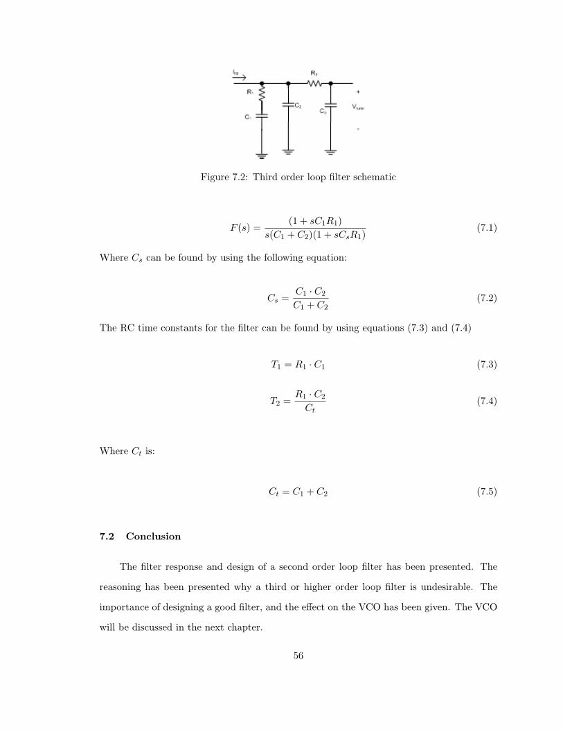
Figure 7.2: Third order loop filter schematic
F (s) =(1 + sC1R1)
s(C1 + C2)(1 + sCsR1)(7.1)
Where Cs can be found by using the following equation:
Cs =C1 · C2
C1 + C2(7.2)
The RC time constants for the filter can be found by using equations (7.3) and (7.4)
T1 = R1 · C1 (7.3)
T2 =R1 · C2
Ct(7.4)
Where Ct is:
Ct = C1 + C2 (7.5)
7.2 Conclusion
The filter response and design of a second order loop filter has been presented. The
reasoning has been presented why a third or higher order loop filter is undesirable. The
importance of designing a good filter, and the effect on the VCO has been given. The VCO
will be discussed in the next chapter.
56
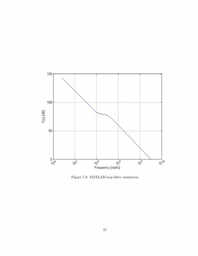
Figure 7.3: MATLAB loop filter simulation
57
Chapter 8
Voltage Controlled Oscillator
An oscillator is any circuit or device that is capable of generating and sustaining pe-
riodic waveforms. Oscillators are used in several places in synthesizers. They can be used
as the reference input to the phase detector, the clock signal for digital circuits, and as the
synthesizer output. There are many design challenges that must be taken into consideration
when dealing with oscillators, such as power dissipation, tuning range, phase noise, and die
area. The largest component in synthesizer design is the inductor used in the resonant
circuit of the oscillator. [31] uses a ring oscillator to eliminate the standard VCO and the
need for bulky inductors. This chapter will discuss some of the more common types of
oscillators, and the design challenges that arise.
8.1 LC Based Oscillators
An LC tank circuit is the central piece to many of the commonly used oscillator struc-
tures. The LC resonator is used to set the oscillation frequency, which can be found by
using (8.1). This oscillation will continue until the resistive losses in the LC resonator decay
the oscillation until the oscillation has stopped. Feedback is commonly used to add energy
to the system to overcome the LC tank losses. The use of varactor diodes in place of the
common capacitor allows for the frequency of the VCO to be tuned by changing the bias
voltage across the diode.
ωosc =1√LC
(8.1)
58
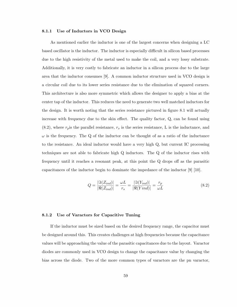
8.1.1 Use of Inductors in VCO Design
As mentioned earlier the inductor is one of the largest concerns when designing a LC
based oscillator is the inductor. The inductor is especially difficult in silicon based processes
due to the high resistivity of the metal used to make the coil, and a very lossy substrate.
Additionally, it is very costly to fabricate an inductor in a silicon process due to the large
area that the inductor consumes [9]. A common inductor structure used in VCO design is
a circular coil due to its lower series resistance due to the elimination of squared corners.
This architecture is also more symmetric which allows the designer to apply a bias at the
center tap of the inductor. This reduces the need to generate two well matched inductors for
the design. It is worth noting that the series resistance pictured in figure 8.1 will actually
increase with frequency due to the skin effect. The quality factor, Q, can be found using
(8.2), where rpis the parallel resistance, rs is the series resistance, L is the inductance, and
ω is the frequency. The Q of the inductor can be thought of as a ratio of the inductance
to the resistance. An ideal inductor would have a very high Q, but current IC processing
techniques are not able to fabricate high Q inductors. The Q of the inductor rises with
frequency until it reaches a resonant peak, at this point the Q drops off as the parasitic
capacitances of the inductor begin to dominate the impedance of the inductor [9] [10].
Q =|=(Zind)||<(Zind)|
=ωL
rs=|=(Yind)||<(Y ind)|
=rpωL
(8.2)
8.1.2 Use of Varactors for Capacitive Tuning
If the inductor must be sized based on the desired frequency range, the capacitor must
be designed around this. This creates challenges at high frequencies because the capacitance
values will be approaching the value of the parasitic capacitances due to the layout. Varactor
diodes are commonly used in VCO design to change the capacitance value by changing the
bias across the diode. Two of the more common types of varactors are the pn varactor,
59
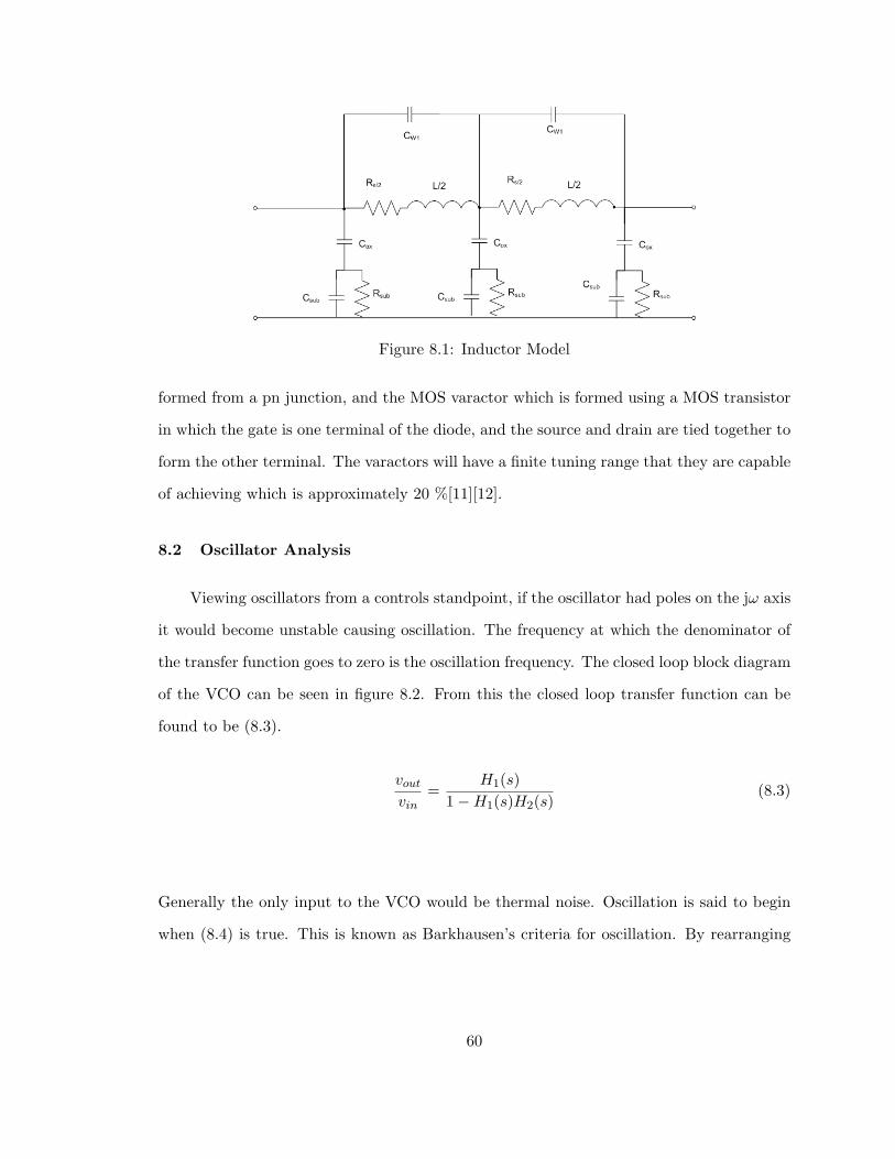
Figure 8.1: Inductor Model
formed from a pn junction, and the MOS varactor which is formed using a MOS transistor
in which the gate is one terminal of the diode, and the source and drain are tied together to
form the other terminal. The varactors will have a finite tuning range that they are capable
of achieving which is approximately 20 %[11][12].
8.2 Oscillator Analysis
Viewing oscillators from a controls standpoint, if the oscillator had poles on the jω axis
it would become unstable causing oscillation. The frequency at which the denominator of
the transfer function goes to zero is the oscillation frequency. The closed loop block diagram
of the VCO can be seen in figure 8.2. From this the closed loop transfer function can be
found to be (8.3).
voutvin
=H1(s)
1−H1(s)H2(s)(8.3)
Generally the only input to the VCO would be thermal noise. Oscillation is said to begin
when (8.4) is true. This is known as Barkhausen’s criteria for oscillation. By rearranging
60
Figure 8.2: Barkhausen criteria block diagram
it can be seen that (8.4) is equal to (8.5) and (8.6)
H1(s)H2(s) = 1 (8.4)
|H1(s)H2(s)|(s) = 1 (8.5)
∠H1(s)H2(s) = 0 or 2nπ (8.6)
8.3 Oscillator Circuit Implementations
The following section will present some of the oscillator circuit implementations. Some
brief analysis will be given as well as potential pitfalls of each design.
8.3.1 Colpitts Oscillator
The Colpitts oscillator uses a single transistor with a resonant circuit to sustain oscil-
lation. In this analysis a NMOS transistor will be used. Figure 8.3 shows the schematic of
the basic Colpitts oscillator. A single inductor along with the series combination of C1 and
C2. C1 and C2 can be varactors to give the ability to tune the the oscillation. In figure
8.4 the Colpitts can be seen with the NMOS transistor replaced with the equivalent small
signal model. From this diagram the resonant frequency can be found to be (8.7). It can
then be found that for oscillation to continue the gain must be (8.8) For many applications
61
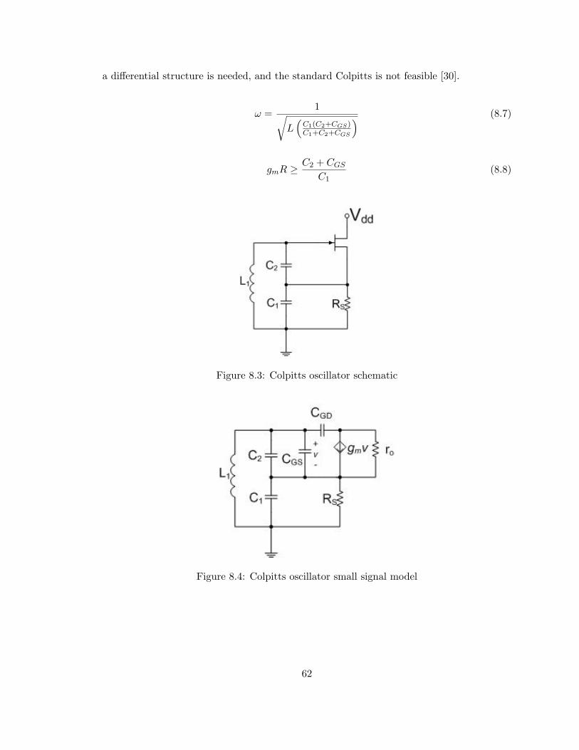
a differential structure is needed, and the standard Colpitts is not feasible [30].
ω =1√
L(C1(C2+CGS)C1+C2+CGS
) (8.7)
gmR ≥C2 + CGS
C1(8.8)
Figure 8.3: Colpitts oscillator schematic
Figure 8.4: Colpitts oscillator small signal model
62
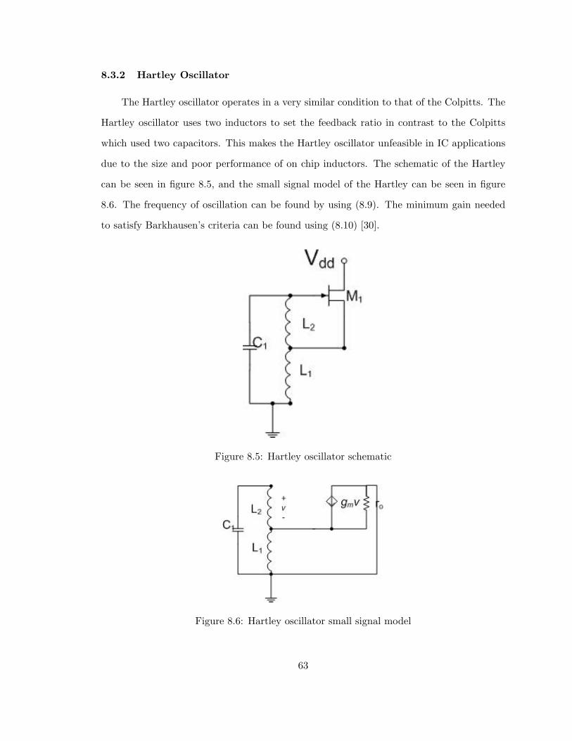
8.3.2 Hartley Oscillator
The Hartley oscillator operates in a very similar condition to that of the Colpitts. The
Hartley oscillator uses two inductors to set the feedback ratio in contrast to the Colpitts
which used two capacitors. This makes the Hartley oscillator unfeasible in IC applications
due to the size and poor performance of on chip inductors. The schematic of the Hartley
can be seen in figure 8.5, and the small signal model of the Hartley can be seen in figure
8.6. The frequency of oscillation can be found by using (8.9). The minimum gain needed
to satisfy Barkhausen’s criteria can be found using (8.10) [30].
Figure 8.5: Hartley oscillator schematic
Figure 8.6: Hartley oscillator small signal model
63
ω =1√
C(L1 + L2)(8.9)
1 + gmro ≥L1
L2(8.10)
8.3.3 Cross-Coupled VCO
The cross-coupled −gm oscillator is one of the most common types of oscillators due to
its simplicity. The cross-coupled −gm oscillator can be seen in figure 8.7. The LC resonator
is comprised of an inductor and a pair of varactors. The resonance frequency can be found
by using (8.1). Both of the bipolar transistors used in the oscillator can be thought of as
common emitter amplifiers. The other transistor is then used as feedback in the form of a
common base amplifier. In order for the oscillation to sustain Barkhausen’s Criteria must
be met. Also, the parallel losses in the LC resonator must be overcome for the oscillations
to continue. Therefore, the impedance looking into the collectors of the bipolar transistors
must be a negative impedance greater than the losses in the tank. By applying a voltage vi
across the collectors of Q1 and Q2 the current can be found using (8.11), where re is 1/gm.
The input impedance can then be found to be (8.12). This can then be used to determine
a minimum value of gm to sustain oscillation(8.13). With a minimum value of gm the
minimum biasing current can easily be solved for. The coupling capacitors are then added
between the base of one transistor and the collector of the other. This allows the voltage
swing of the oscillator to go above VBE without pushing the transistors into saturation. A
biasing resistors are then connected to the base of each transistor to keep the transistor
correctly DC biased.
ii =vi
re1 + re2= −gm1vπ1 − gm2 (8.11)
Zin = −2re =−2gm
(8.12)
gm >2Rp
(8.13)
64
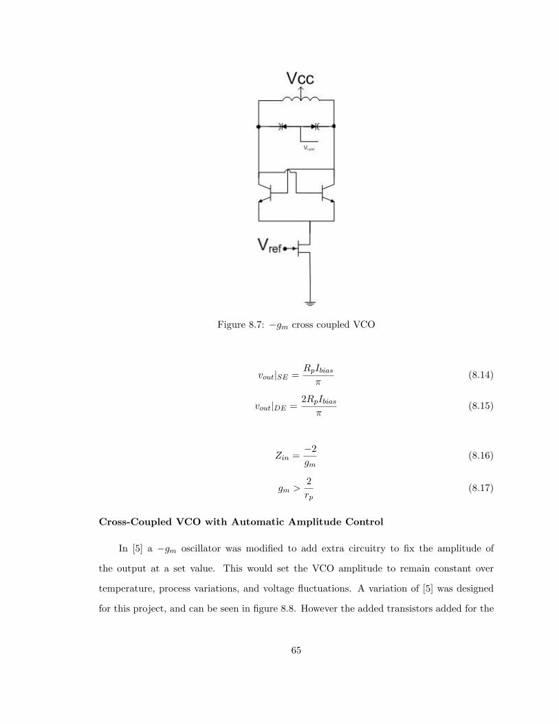
Figure 8.7: −gm cross coupled VCO
vout|SE =RpIbiasπ
(8.14)
vout|DE =2RpIbias
π(8.15)
Zin =−2gm
(8.16)
gm >2rp
(8.17)
Cross-Coupled VCO with Automatic Amplitude Control
In [5] a −gm oscillator was modified to add extra circuitry to fix the amplitude of
the output at a set value. This would set the VCO amplitude to remain constant over
temperature, process variations, and voltage fluctuations. A variation of [5] was designed
for this project, and can be seen in figure 8.8. However the added transistors added for the
65
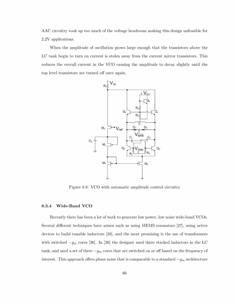
AAC circuitry took up too much of the voltage headroom making this design unfeasible for
2.2V applications.
When the amplitude of oscillation grows large enough that the transistors above the
LC tank begin to turn on current is stolen away from the current mirror transistors. This
reduces the overall current in the VCO causing the amplitude to decay slightly until the
top level transistors are turned off once again.
Figure 8.8: VCO with automatic amplitude control circuitry
8.3.4 Wide-Band VCO
Recently there has been a lot of work to generate low power, low noise wide-band VCOs.
Several different techniques have arisen such as using MEMS resonators [27], using active
devices to build tunable inductors [28], and the most promising is the use of transformers
with switched −gm cores [26]. In [26] the designer used three stacked inductors in the LC
tank, and used a set of three −gm cores that are switched on or off based on the frequency of
interest. This approach offers phase noise that is comparable to a standard −gm architecture
66
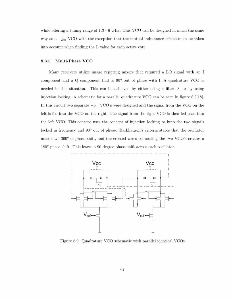
while offering a tuning range of 1.3 - 6 GHz. This VCO can be designed in much the same
way as a −gm VCO with the exception that the mutual inductance effects must be taken
into account when finding the L value for each active core.
8.3.5 Multi-Phase VCO
Many receivers utilize image rejecting mixers that required a LO signal with an I
component and a Q component that is 90o out of phase with I. A quadrature VCO is
needed in this situation. This can be achieved by either using a filter [3] or by using
injection locking. A schematic for a parallel quadrature VCO can be seen in figure 8.9[18].
In this circuit two separate −gm VCO’s were designed and the signal from the VCO on the
left is fed into the VCO on the right. The signal from the right VCO is then fed back into
the left VCO. This concept uses the concept of injection locking to keep the two signals
locked in frequency and 90o out of phase. Barkhausen’s criteria states that the oscillator
must have 360o of phase shift, and the crossed wires connecting the two VCO’s creates a
180o phase shift. This leaves a 90 degree phase shift across each oscillator.
Figure 8.9: Quadrature VCO schematic with parallel identical VCOs
67
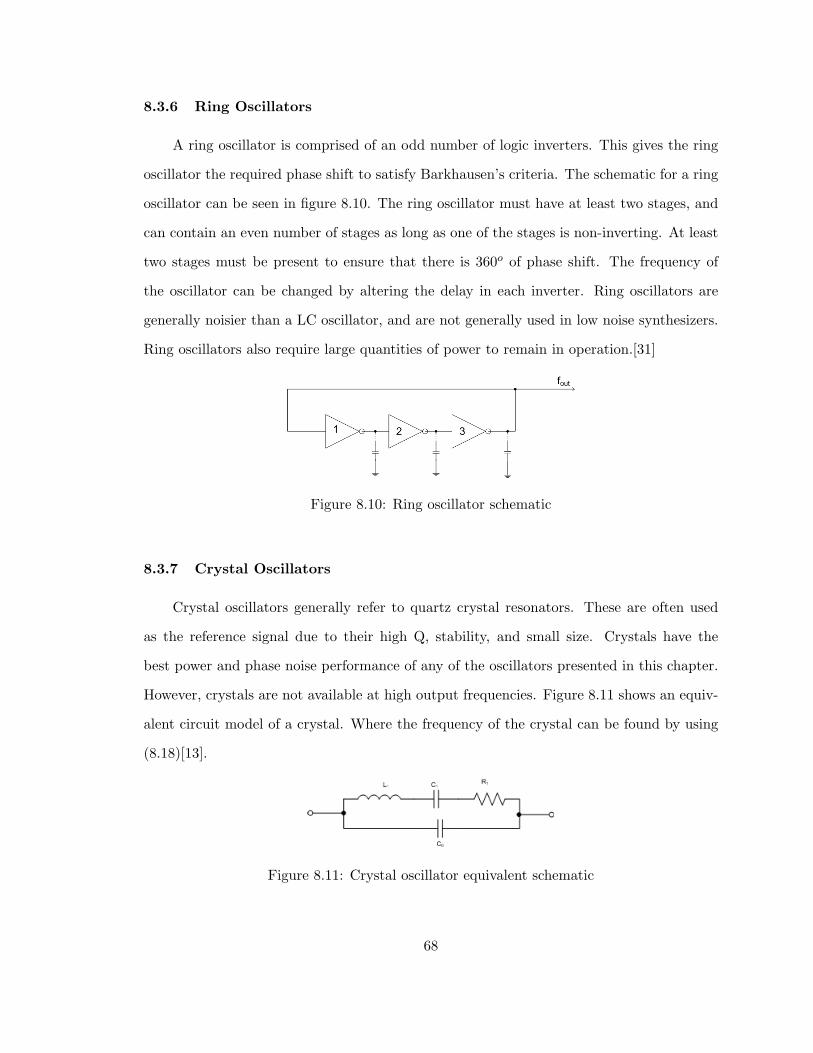
8.3.6 Ring Oscillators
A ring oscillator is comprised of an odd number of logic inverters. This gives the ring
oscillator the required phase shift to satisfy Barkhausen’s criteria. The schematic for a ring
oscillator can be seen in figure 8.10. The ring oscillator must have at least two stages, and
can contain an even number of stages as long as one of the stages is non-inverting. At least
two stages must be present to ensure that there is 360o of phase shift. The frequency of
the oscillator can be changed by altering the delay in each inverter. Ring oscillators are
generally noisier than a LC oscillator, and are not generally used in low noise synthesizers.
Ring oscillators also require large quantities of power to remain in operation.[31]
Figure 8.10: Ring oscillator schematic
8.3.7 Crystal Oscillators
Crystal oscillators generally refer to quartz crystal resonators. These are often used
as the reference signal due to their high Q, stability, and small size. Crystals have the
best power and phase noise performance of any of the oscillators presented in this chapter.
However, crystals are not available at high output frequencies. Figure 8.11 shows an equiv-
alent circuit model of a crystal. Where the frequency of the crystal can be found by using
(8.18)[13].
Figure 8.11: Crystal oscillator equivalent schematic
68
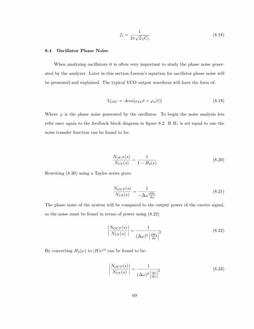
fs =1
2π√L1C1
(8.18)
8.4 Oscillator Phase Noise
When analyzing oscillators it is often very important to study the phase noise gener-
ated by the analyzer. Later in this section Leeson’s equation for oscillator phase noise will
be presented and explained. The typical VCO output waveform will have the form of:
VOSC = Acos[ωLOt+ ϕn(t)] (8.19)
Where ϕ is the phase noise generated by the oscillator. To begin the noise analysis lets
refer once again to the feedback block diagram in figure 8.2. If H1 is set equal to one the
noise transfer function can be found to be:
NOUT (s)NIN (s)
=1
1−H2(s)(8.20)
Rewriting (8.20) using a Taylor series gives:
NOUT (s)NIN (s)
=1
−∆ω dH2dω
(8.21)
The phase noise of the system will be compared to the output power of the carrier signal,
so the noise must be found in terms of power using (8.22)
∣∣∣∣NOUT (s)NIN (s)
∣∣∣∣ =1
(∆ω)2∣∣∣dH2dω
∣∣∣2 (8.22)
By converting H2(ω) to |H|ejφ can be found to be:
∣∣∣∣NOUT (s)NIN (s)
∣∣∣∣ =1
(∆ω)2∣∣∣ dφdω ∣∣∣2 (8.23)
69
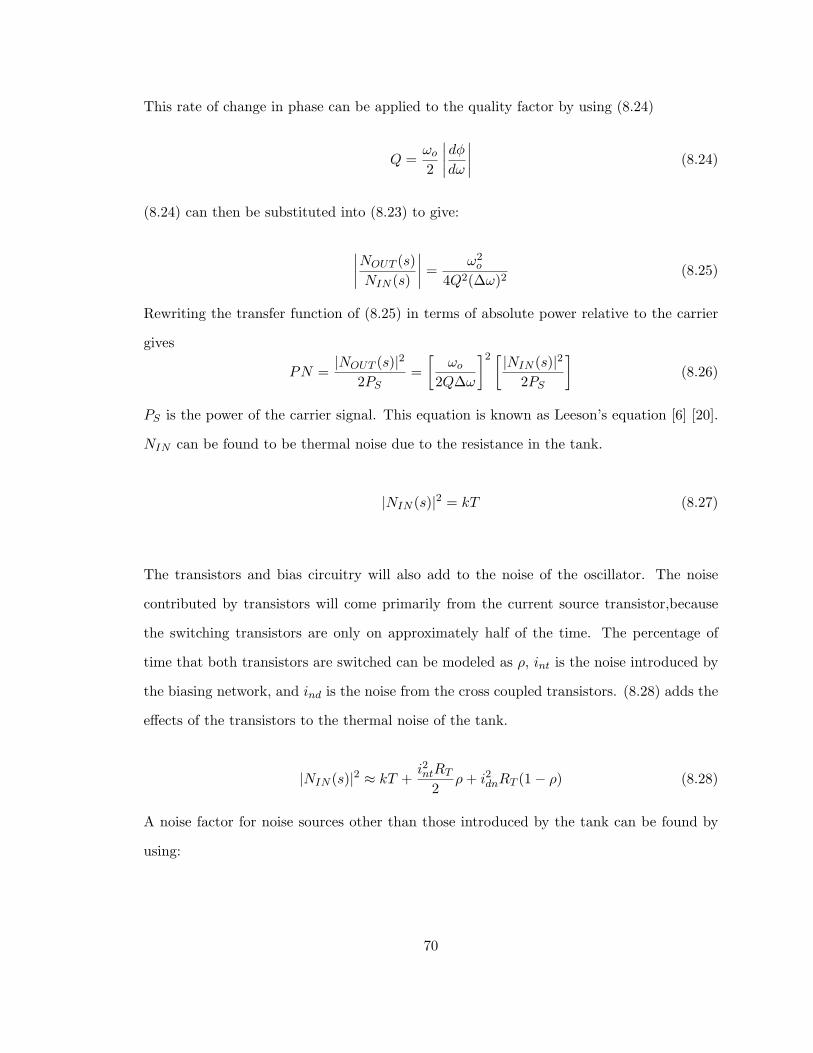
This rate of change in phase can be applied to the quality factor by using (8.24)
Q =ωo2
∣∣∣∣dφdω∣∣∣∣ (8.24)
(8.24) can then be substituted into (8.23) to give:
∣∣∣∣NOUT (s)NIN (s)
∣∣∣∣ =ω2o
4Q2(∆ω)2(8.25)
Rewriting the transfer function of (8.25) in terms of absolute power relative to the carrier
gives
PN =|NOUT (s)|2
2PS=[
ωo2Q∆ω
]2 [ |NIN (s)|2
2PS
](8.26)
PS is the power of the carrier signal. This equation is known as Leeson’s equation [6] [20].
NIN can be found to be thermal noise due to the resistance in the tank.
|NIN (s)|2 = kT (8.27)
The transistors and bias circuitry will also add to the noise of the oscillator. The noise
contributed by transistors will come primarily from the current source transistor,because
the switching transistors are only on approximately half of the time. The percentage of
time that both transistors are switched can be modeled as ρ, int is the noise introduced by
the biasing network, and ind is the noise from the cross coupled transistors. (8.28) adds the
effects of the transistors to the thermal noise of the tank.
|NIN (s)|2 ≈ kT +i2ntRT
2ρ+ i2dnRT (1− ρ) (8.28)
A noise factor for noise sources other than those introduced by the tank can be found by
using:
70
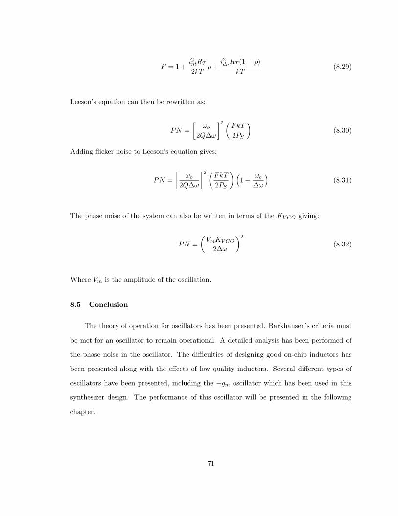
F = 1 +i2ntRT2kT
ρ+i2dnRT (1− ρ)
kT(8.29)
Leeson’s equation can then be rewritten as:
PN =[
ωo2Q∆ω
]2(FkT2PS
)(8.30)
Adding flicker noise to Leeson’s equation gives:
PN =[
ωo2Q∆ω
]2(FkT2PS
)(1 +
ωc∆ω
)(8.31)
The phase noise of the system can also be written in terms of the KV CO giving:
PN =(VmKV CO
2∆ω
)2
(8.32)
Where Vm is the amplitude of the oscillation.
8.5 Conclusion
The theory of operation for oscillators has been presented. Barkhausen’s criteria must
be met for an oscillator to remain operational. A detailed analysis has been performed of
the phase noise in the oscillator. The difficulties of designing good on-chip inductors has
been presented along with the effects of low quality inductors. Several different types of
oscillators have been presented, including the −gm oscillator which has been used in this
synthesizer design. The performance of this oscillator will be presented in the following
chapter.
71
Chapter 9
Simulated and Measured Fractional-N PLL Design and Results
The previous section presented several different types of VCO’s as well as the theory of
operation behind oscillators. This chapter will present the process that was used to verify
the VCO and PLL through simulation and testing.
9.1 VCO Design
The final schematic of the VCO can be seen in figure 9.1. The inductor and varactors
were sized to give the VCO a center frequency of 13 GHz at the middle of the voltage tuning
range. The biasing current for the VCO was chosen to be 8 mA. 4 mA was found to be
sufficient current, but it was decided to use 8 mA to provide a larger voltage swing as well
as providing a buffer for the loading effect of supporting circuitry and effects of the layout.
After the VCO had been completed some additional circuitry was needed to test the VCO,
and to drive the MMD.
9.2 VCO Support Circuitry
There were several small circuits that needed to be designed in order to interface the
VCO with the rest of the synthesizer. The output of the VCO was fed into a pair of emitter
followers to ensure that there was not excessive loading placed on the output of the VCO.
The emitter follower schematic can be seen in figure 9.2.
The next support circuit developed was capacitive divider buffer circuit. This used a
capacitor divider to reduce the AC magnitude of the oscillation to prevent the CML buffers
interfacing the VCO to the MMD from entering breakdown. The output of the capacitive
dividers are fed into the input of a differential pair buffer with enough drive strength to
72
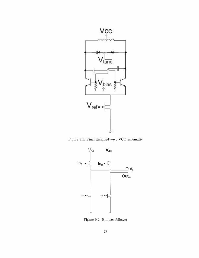
Figure 9.1: Final designed −gm VCO schematic
Figure 9.2: Emitter follower
73
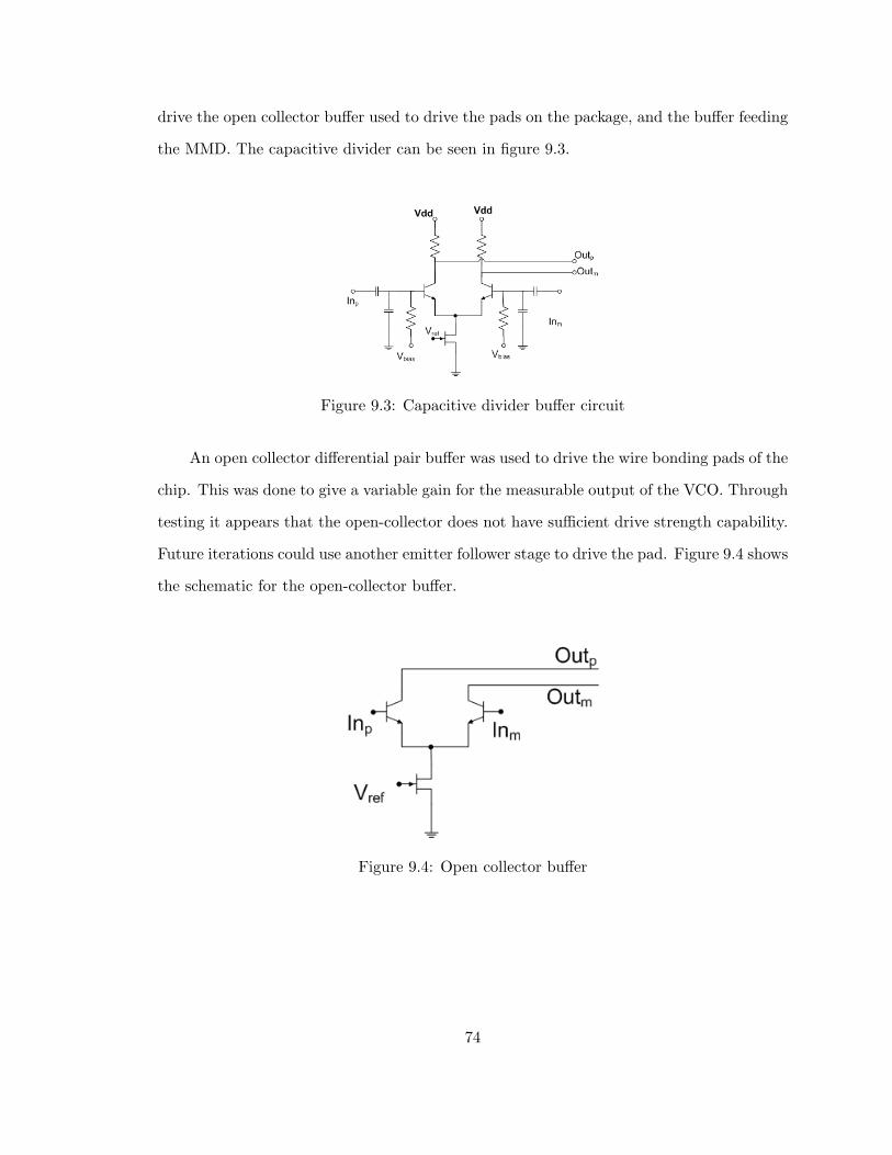
drive the open collector buffer used to drive the pads on the package, and the buffer feeding
the MMD. The capacitive divider can be seen in figure 9.3.
Figure 9.3: Capacitive divider buffer circuit
An open collector differential pair buffer was used to drive the wire bonding pads of the
chip. This was done to give a variable gain for the measurable output of the VCO. Through
testing it appears that the open-collector does not have sufficient drive strength capability.
Future iterations could use another emitter follower stage to drive the pad. Figure 9.4 shows
the schematic for the open-collector buffer.
Figure 9.4: Open collector buffer
74
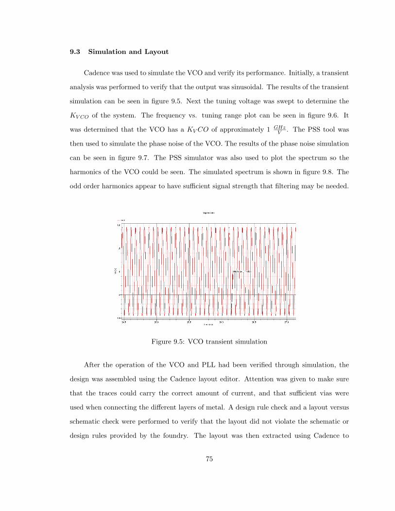
9.3 Simulation and Layout
Cadence was used to simulate the VCO and verify its performance. Initially, a transient
analysis was performed to verify that the output was sinusoidal. The results of the transient
simulation can be seen in figure 9.5. Next the tuning voltage was swept to determine the
KV CO of the system. The frequency vs. tuning range plot can be seen in figure 9.6. It
was determined that the VCO has a KV CO of approximately 1 GHzV . The PSS tool was
then used to simulate the phase noise of the VCO. The results of the phase noise simulation
can be seen in figure 9.7. The PSS simulator was also used to plot the spectrum so the
harmonics of the VCO could be seen. The simulated spectrum is shown in figure 9.8. The
odd order harmonics appear to have sufficient signal strength that filtering may be needed.
Figure 9.5: VCO transient simulation
After the operation of the VCO and PLL had been verified through simulation, the
design was assembled using the Cadence layout editor. Attention was given to make sure
that the traces could carry the correct amount of current, and that sufficient vias were
used when connecting the different layers of metal. A design rule check and a layout versus
schematic check were performed to verify that the layout did not violate the schematic or
design rules provided by the foundry. The layout was then extracted using Cadence to
75
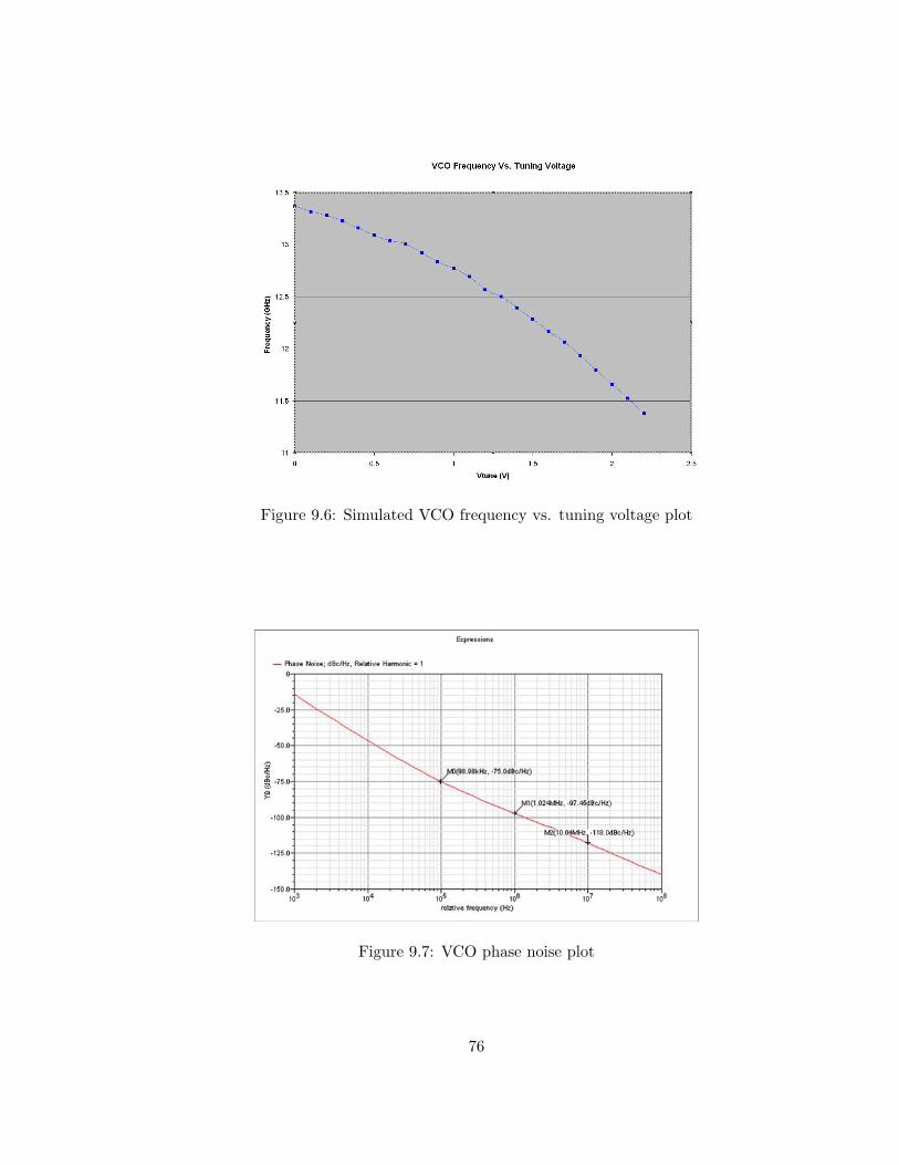
Figure 9.6: Simulated VCO frequency vs. tuning voltage plot
Figure 9.7: VCO phase noise plot
76
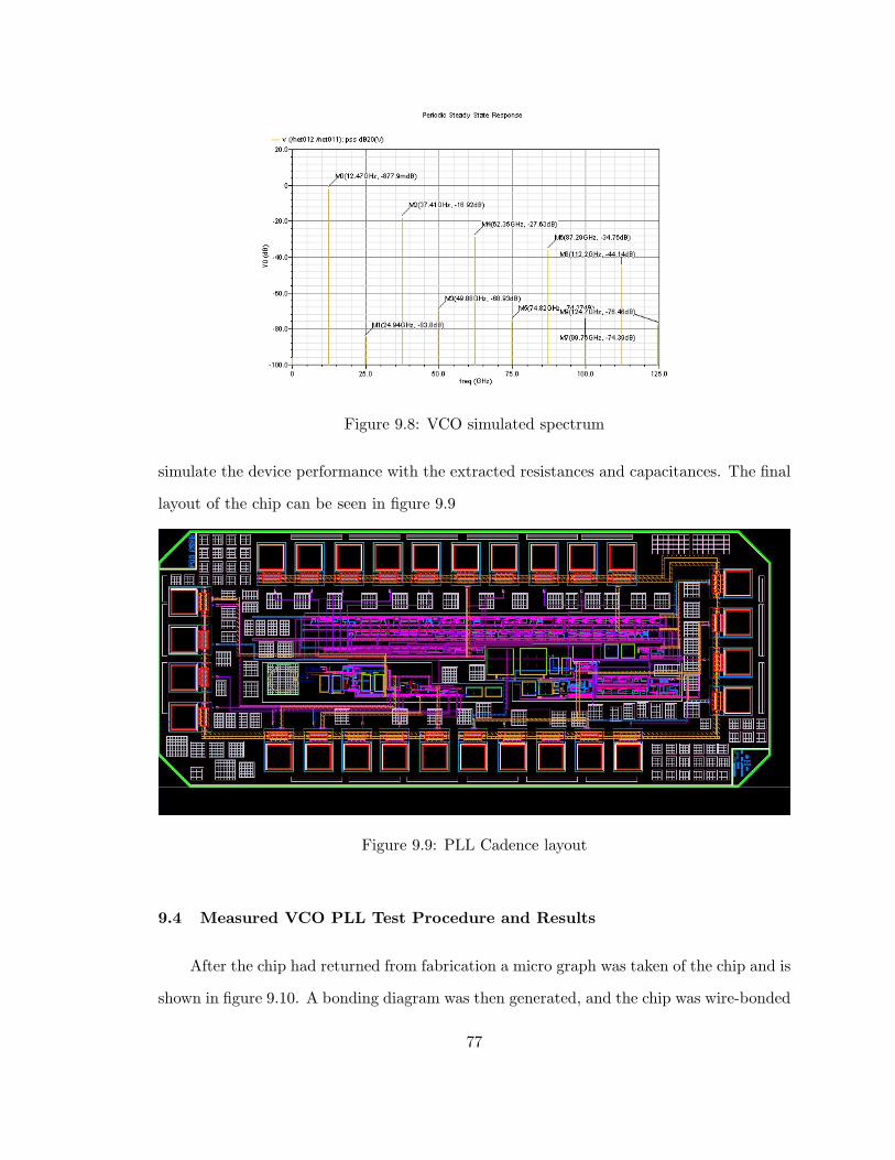
Figure 9.8: VCO simulated spectrum
simulate the device performance with the extracted resistances and capacitances. The final
layout of the chip can be seen in figure 9.9
Figure 9.9: PLL Cadence layout
9.4 Measured VCO PLL Test Procedure and Results
After the chip had returned from fabrication a micro graph was taken of the chip and is
shown in figure 9.10. A bonding diagram was then generated, and the chip was wire-bonded
77
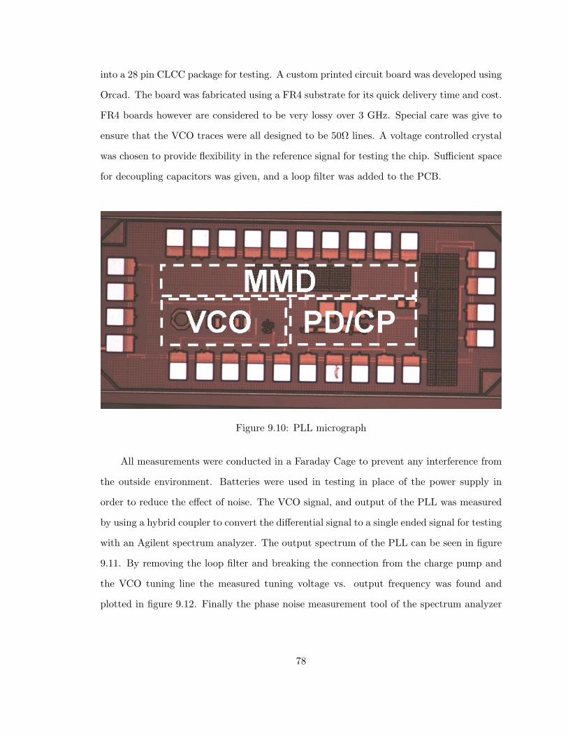
into a 28 pin CLCC package for testing. A custom printed circuit board was developed using
Orcad. The board was fabricated using a FR4 substrate for its quick delivery time and cost.
FR4 boards however are considered to be very lossy over 3 GHz. Special care was give to
ensure that the VCO traces were all designed to be 50Ω lines. A voltage controlled crystal
was chosen to provide flexibility in the reference signal for testing the chip. Sufficient space
for decoupling capacitors was given, and a loop filter was added to the PCB.
Figure 9.10: PLL micrograph
All measurements were conducted in a Faraday Cage to prevent any interference from
the outside environment. Batteries were used in testing in place of the power supply in
order to reduce the effect of noise. The VCO signal, and output of the PLL was measured
by using a hybrid coupler to convert the differential signal to a single ended signal for testing
with an Agilent spectrum analyzer. The output spectrum of the PLL can be seen in figure
9.11. By removing the loop filter and breaking the connection from the charge pump and
the VCO tuning line the measured tuning voltage vs. output frequency was found and
plotted in figure 9.12. Finally the phase noise measurement tool of the spectrum analyzer
78
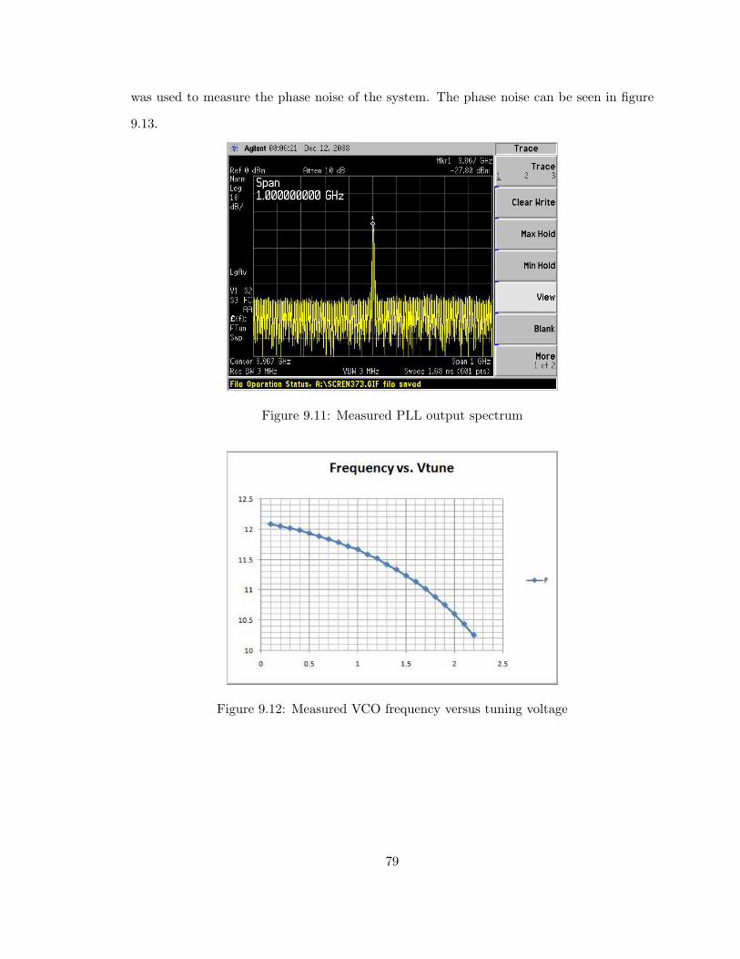
was used to measure the phase noise of the system. The phase noise can be seen in figure
9.13.
Figure 9.11: Measured PLL output spectrum
Figure 9.12: Measured VCO frequency versus tuning voltage
79
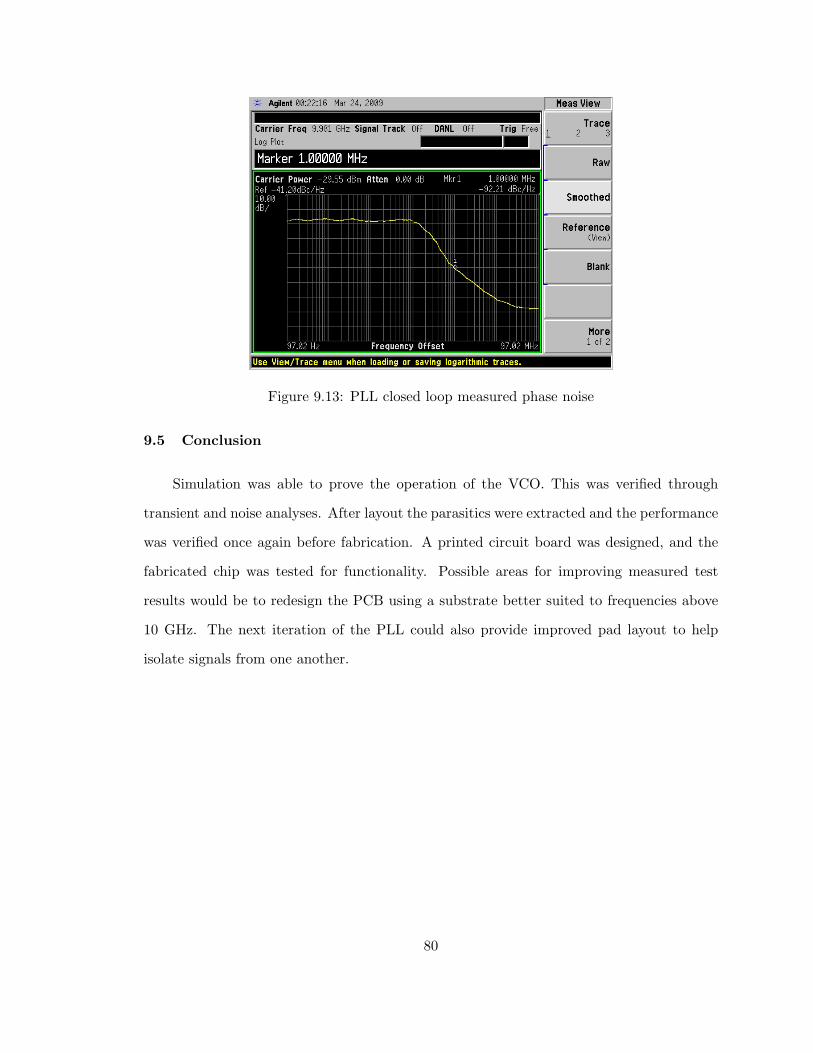
Figure 9.13: PLL closed loop measured phase noise
9.5 Conclusion
Simulation was able to prove the operation of the VCO. This was verified through
transient and noise analyses. After layout the parasitics were extracted and the performance
was verified once again before fabrication. A printed circuit board was designed, and the
fabricated chip was tested for functionality. Possible areas for improving measured test
results would be to redesign the PCB using a substrate better suited to frequencies above
10 GHz. The next iteration of the PLL could also provide improved pad layout to help
isolate signals from one another.
80
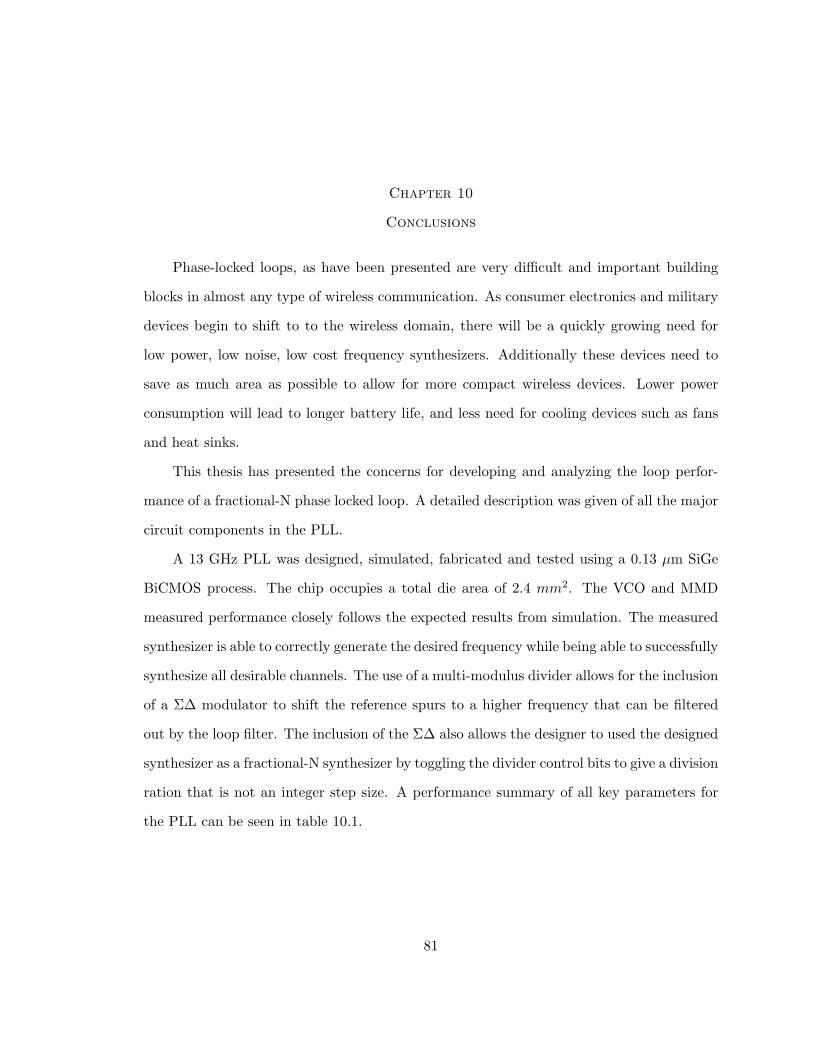
Chapter 10
Conclusions
Phase-locked loops, as have been presented are very difficult and important building
blocks in almost any type of wireless communication. As consumer electronics and military
devices begin to shift to to the wireless domain, there will be a quickly growing need for
low power, low noise, low cost frequency synthesizers. Additionally these devices need to
save as much area as possible to allow for more compact wireless devices. Lower power
consumption will lead to longer battery life, and less need for cooling devices such as fans
and heat sinks.
This thesis has presented the concerns for developing and analyzing the loop perfor-
mance of a fractional-N phase locked loop. A detailed description was given of all the major
circuit components in the PLL.
A 13 GHz PLL was designed, simulated, fabricated and tested using a 0.13 µm SiGe
BiCMOS process. The chip occupies a total die area of 2.4 mm2. The VCO and MMD
measured performance closely follows the expected results from simulation. The measured
synthesizer is able to correctly generate the desired frequency while being able to successfully
synthesize all desirable channels. The use of a multi-modulus divider allows for the inclusion
of a Σ∆ modulator to shift the reference spurs to a higher frequency that can be filtered
out by the loop filter. The inclusion of the Σ∆ also allows the designer to used the designed
synthesizer as a fractional-N synthesizer by toggling the divider control bits to give a division
ration that is not an integer step size. A performance summary of all key parameters for
the PLL can be seen in table 10.1.
81
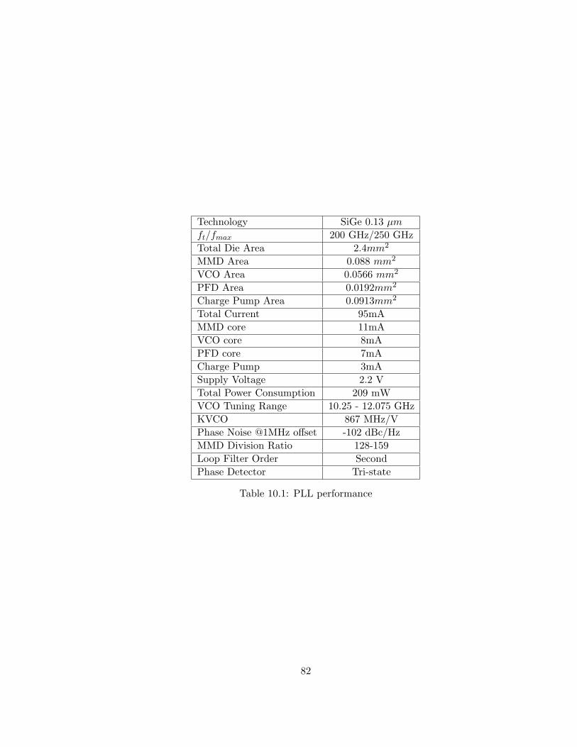
Technology SiGe 0.13 µmft/fmax 200 GHz/250 GHzTotal Die Area 2.4mm2
MMD Area 0.088 mm2
VCO Area 0.0566 mm2
PFD Area 0.0192mm2
Charge Pump Area 0.0913mm2
Total Current 95mAMMD core 11mAVCO core 8mAPFD core 7mACharge Pump 3mASupply Voltage 2.2 VTotal Power Consumption 209 mWVCO Tuning Range 10.25 - 12.075 GHzKVCO 867 MHz/VPhase Noise @1MHz offset -102 dBc/HzMMD Division Ratio 128-159Loop Filter Order SecondPhase Detector Tri-state
Table 10.1: PLL performance
82
Bibliography
[1] Ray, M.; Souder, W.; Ratcliff, M.; Dai, F.; Irwin, J. D.; “A 13GHz Low Power Multi-Modulus Divider Implemented in 0.13µm SiGe Technology” Silicon Monolithic Inte-grated Circuits in RF Systems, 2009. SiRF ’09. IEEE Topical Meeting on 19-21 Jan.2009 Page(s):1 - 4
[2] J. Rogers, C. Plett, F. Dai; Integrated Circuit Design for High Speed Frequency Syn-thesis, Norwood, MA: Artech House, 2006.
[3] Rogers, J., Plett, C.; Radio Frequency Integrated Circuit Design, Norwood, MA: ArtechHouse, 2003.
[4] Jaeger,R., Blalock, T.;Microelectronic Circuit Design 2nd Edition, :New York,NY: Mc-Graw Hill, 2004; pp.463-504
[5] Rogers, John; Rahn, David; Plett, Calvin; “A Study of Digital and Analog Automatic-Amplitude Control Circuitry for Voltage-Controlled Oscillators,”IEEE Journal of Solid-State Circuits, VOL. 38, NO. 2, February 2003 pp. 352 - 356
[6] Leeson, D.B.; “A Simple Model of Feedback Oscillator Noise Spectrum,”Proc. IEEE,February 1966, pp. 329-330
[7] Kroupa, V.F.; “Noise Properties of PLL Systems,” IEEE Trans. on Communications,Vol. 30, October 1982 pp. 2244-2252
[8] Kroupa, V.F.; “Jitter and Phase Noise in Frequency Dividers,” IEEE Trans. on Instru-mentation and Measurement, Vol. 50, No. 5, October 2001 pp. p1241
[9] Long, J.R.; Copeland, M.A. “The modeling,Characterization, and Design of MonolithicInductors for Silicon RFIC’s,”IEEE Journal of Solid-State Circuits, VOL. 32, March1997 pp. 357 - 369
[10] Niknejad, A.M, and R.G Meyer; “Analysis, Design, and Optimization of Spiral Induc-tors and Transformers for Si RF IC’s,”IEEE Journal of Solid-State Circuits, VOL. 33,October 1998 pp. 1470 - 1481
[11] Andreani, P., and S. Mattison; “On the Use of MOS Varactors in RF VCOs,”IEEEJournal of Solid-State Circuits, VOL. 35, NO. 6, June 2002 pp. 905 - 910
[12] Fong, N. ; “Accumulation MOS Varactors for 4 to 40 GHz VCOs in SOI CMOS,”Proc.2002 International SOI Conference, October 2002 pp. 158-160
83
[13] Vig, J.R.; “Quartz Crystal Resonators and Oscillators,”U.S. Army Electronics Tech-nology and Devices Report, SLCET-TR-88-1, 1988
[14] Rogers, J.W.M.; “A Fully Integrated Multi-Band Σ∆ Fractional-N Frequency Synthe-sizer for a MIMO WLAN Transceiver RFIC,”IEEE Journal of Solid-State Circuits,VOL. 40, NO. 3, March 2005 pp. 678-689
[15] Lee, J.; Kim, B.; “A Low-Noise Fast-Lock Phase-Locked Loop with Adaptive Band-width Control,”IEEE Journal of Solid-State Circuits, VOL. 35, NO. 8, August 2005pp. 1137 - 1145
[16] Sandireddy, R.; Dai, F.; Jaeger, R.; “A Generic Architecture for Multi-Modulus Di-viders in Low-Power and High-Speed Frequency Synthesis,”IEEE 5th Topical Meetingon Silicon Monolithic Integrated Circuits in RF Systems, September 2004 pp. 243 - 246
[17] Vaucher, C.S.; Ferencic, I; Locher, M; Sedvallson, S.;Voegeli, U.; Wang, Z; “A familyof low-power truly modular programmable dividers in standard 0.35 µm CMOS tech-nology,”IEEE Journal of Solid-State Circuits, VOL. 35, NO. 7, July 2000 pp. 1039 -1045
[18] Kakani, V.; Dai, F.F.; Jaeger, R.C.; “ A 5GHz Series Coupled BiCMOS QuadratureVCO with Wide Tuning Range,”Bipolar/BiCMOS Circuits and Technology Meeting,2006 Oct. 2006 pp. 1 - 4
[19] Rogers, J., Plett, C., Dai, F.; Integrated Circuit Design for High Speed FrequencySynthesis, Norwood, MA: Artech House, 2006.
[20] Rogers, J., Plett, C., Dai, F.; Integrated Circuit Design for High Speed FrequencySynthesis, Norwood, MA: Artech House, 2006.
[21] Tierney, J.; Rader,C., Gold, B.;“A Digital Frequency Synthesizer”IEEE Trans. AudioElectroacoust., Vol. AU-19, 1971, pp. 48-57
[22] Ultra High Speed Phase/Frequency Discriminator, AD9901 1999, Analog Devices prod-uct data sheet, 1999, http://www.analog.com/en/prod/0,2877,AD9901,00.html
[23] Craninckx, J., Steaert, M.S.;“A Fully Integrated CMOS DCS-1800 Frequency Synthe-sizer,” IEEE J. Solid State Circuits, Vol. 33, December 1998, pp. 2054-2065
[24] Rogers, J., Plett, C., Dai, F.; Integrated Circuit Design for High Speed FrequencySynthesis, Norwood, MA: Artech House, 2006.
[25] Rogers, J., Plett, C., Dai, F.; Integrated Circuit Design for High Speed FrequencySynthesis, Norwood, MA: Artech House, 2006.
[26] Safarian, Z. ;Hashemi, H. ; “A 1.3-6 GHz Triple-Mode CMOS VCO Using CoupledInductors,” Custom Integrated Circuits Conference, 2008. CICC 2008. IEEE pp. 69-72
[27] Darade, B.S.;“ Low phase noise wide band VCO using MEMS,”Circuits and Systems,2005. 48th Midwest Symposium on Vol. 1 Aug. 2005 pp.155 - 158
84
[28] Lu, L.H., Hsieh, H.H., Liao, Y.T.; “A Wide Tuning-Range CMOS VCO With a Dif-ferential Tunable Active Inductor,”IEEE Transaction on Microwave Theory and tech-niques VOL. 54, NO. 9, September 2006 pp. 3462 - 3468
[29] Rogers, J., Plett, C., Dai, F.; Integrated Circuit Design for High Speed FrequencySynthesis, Norwood, MA: Artech House, 2006.
[30] Jaeger, R., Blalock, T.;Microelectronic Circuit Design 2nd Edition, :New York,NY:McGraw Hill, 2004; pp. 1449-1461
[31] Dai, L.; Harjani, R;“Design of Low-Phase Noise CMOS Ring Oscillators,”IEEE Tran.Circuits and Systems II, VOL. 49, NO. 5, May 2002 pp. 328 - 338
85

Appendices
86
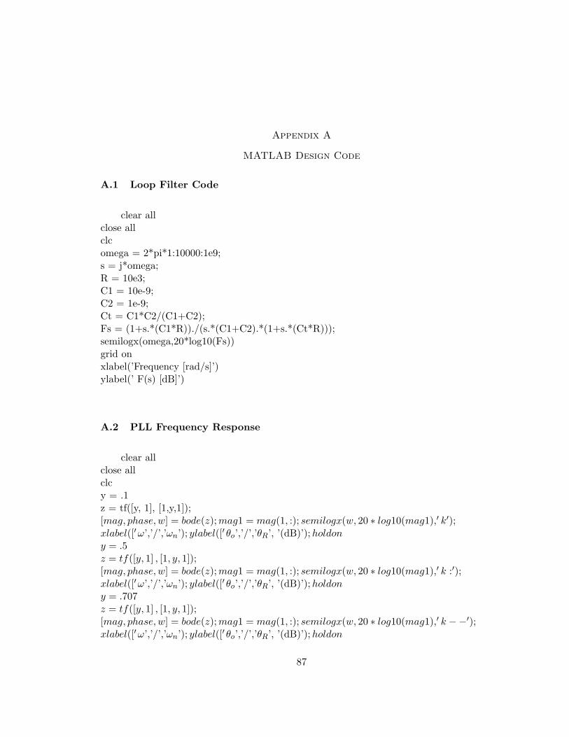
Appendix A
MATLAB Design Code
A.1 Loop Filter Code
clear allclose allclcomega = 2*pi*1:10000:1e9;s = j*omega;R = 10e3;C1 = 10e-9;C2 = 1e-9;Ct = C1*C2/(C1+C2);Fs = (1+s.*(C1*R))./(s.*(C1+C2).*(1+s.*(Ct*R)));semilogx(omega,20*log10(Fs))grid onxlabel(’Frequency [rad/s]’)ylabel(’ F(s) [dB]’)
A.2 PLL Frequency Response
clear allclose allclcy = .1z = tf([y, 1], [1,y,1]);[mag, phase, w] = bode(z);mag1 = mag(1, :); semilogx(w, 20 ∗ log10(mag1),′ k′);xlabel([′ω’,’/’,’ωn’); ylabel([′ θo’,’/’,’θR’, ’(dB)’);holdony = .5z = tf([y, 1] , [1, y, 1]);[mag, phase, w] = bode(z);mag1 = mag(1, :); semilogx(w, 20 ∗ log10(mag1),′ k :′);xlabel([′ω’,’/’,’ωn’); ylabel([′ θo’,’/’,’θR’, ’(dB)’);holdony = .707z = tf([y, 1] , [1, y, 1]);[mag, phase, w] = bode(z);mag1 = mag(1, :); semilogx(w, 20 ∗ log10(mag1),′ k −−′);xlabel([′ω’,’/’,’ωn’); ylabel([′ θo’,’/’,’θR’, ’(dB)’);holdon
87
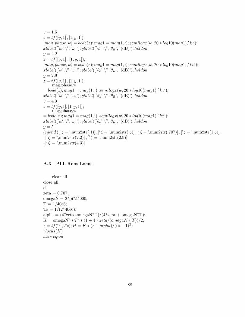
y = 1.5z = tf([y, 1] , [1, y, 1]);[mag, phase, w] = bode(z);mag1 = mag(1, :); semilogx(w, 20 ∗ log10(mag1),′ k.′);xlabel([′ω’,’/’,’ωn’); ylabel([′ θo’,’/’,’θR’, ’(dB)’);holdony = 2.2z = tf([y, 1] , [1, y, 1]);[mag, phase, w] = bode(z);mag1 = mag(1, :); semilogx(w, 20 ∗ log10(mag1),′ ko′);xlabel([′ω’,’/’,’ωn’); ylabel([′ θo’,’/’,’θR’, ’(dB)’);holdony = 2.9z = tf([y, 1] , [1, y, 1]);
mag,phase,w= bode(z);mag1 = mag(1, :); semilogx(w, 20 ∗ log10(mag1),′ k :′);xlabel([′ω’,’/’,’ωn’); ylabel([′ θo’,’/’,’θR’, ’(dB)’);holdony = 4.3z = tf([y, 1], [1, y, 1]);
mag,phase,w= bode(z);mag1 = mag(1, :); semilogx(w, 20 ∗ log10(mag1),′ kx′);xlabel([′ω′,’/’,’ωn’); ylabel([′ θo’,’/’,’θR’, ’(dB)’);holdony = 5legend ([′ ζ = ’,num2str(.1)] , [′ ζ = ’,num2str(.5)] , [′ ζ = ’,num2str(.707)] , [′ ζ = ’,num2str(1.5)] ., [′ ζ = ’,num2str(2.2)] , [′ ζ = ’,num2str(2.9)], [′ ζ = ’,num2str(4.3)]
A.3 PLL Root Locus
clear allclose allclczeta = 0.707;omegaN = 2*pi*55000;T = 1/40e6;Ts = 1/(2*40e6);alpha = (4*zeta -omegaN*T)/(4*zeta + omegaN*T);K = omegaN2 ∗ T 2 ∗ (1 + 4 ∗ zeta/(omegaN ∗ T ))/2;z = tf(′z′, T s);H = K ∗ (z − alpha)/((z − 1)2)rlocus(H)axis equal
88
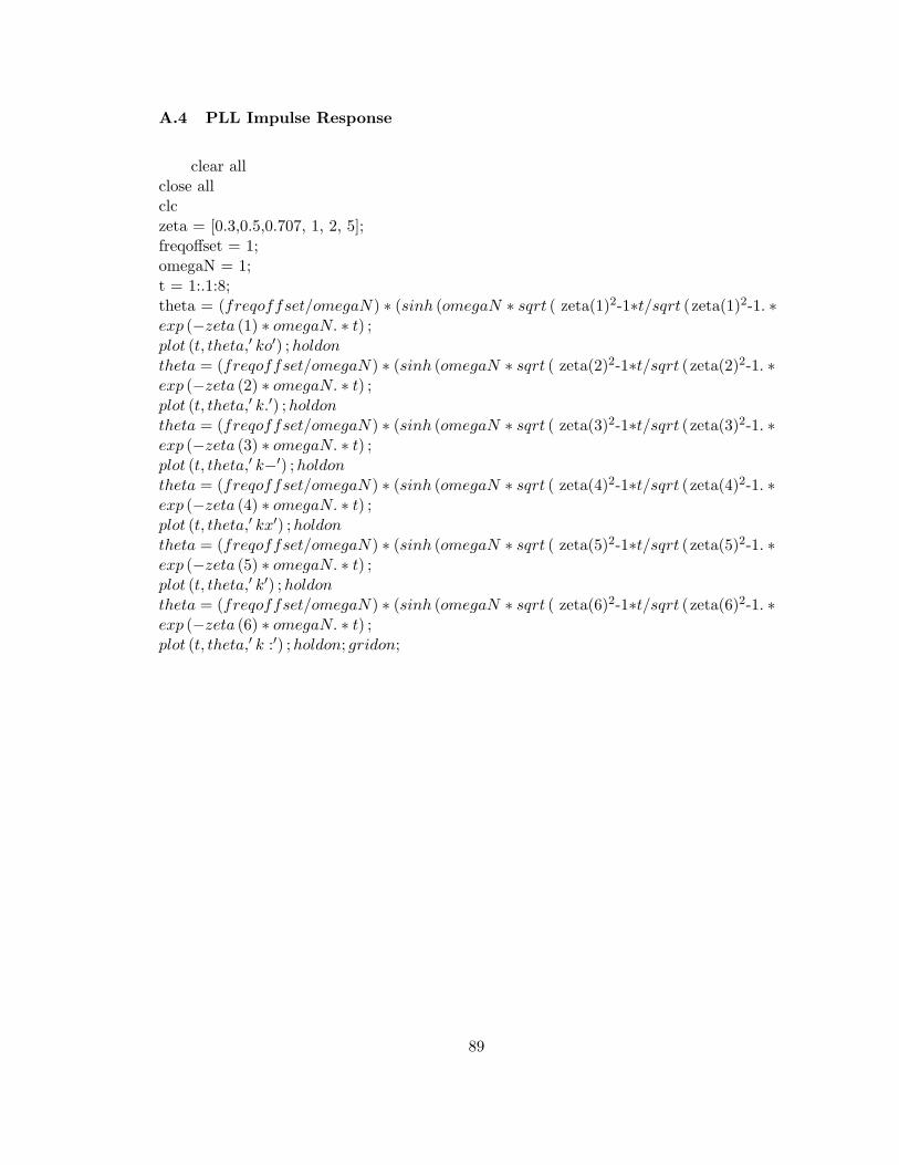
A.4 PLL Impulse Response
clear allclose allclczeta = [0.3,0.5,0.707, 1, 2, 5];freqoffset = 1;omegaN = 1;t = 1:.1:8;theta = (freqoffset/omegaN) ∗ (sinh (omegaN ∗ sqrt ( zeta(1)2-1∗t/sqrt (zeta(1)2-1. ∗exp (−zeta (1) ∗ omegaN. ∗ t) ;plot (t, theta,′ ko′) ;holdontheta = (freqoffset/omegaN) ∗ (sinh (omegaN ∗ sqrt ( zeta(2)2-1∗t/sqrt (zeta(2)2-1. ∗exp (−zeta (2) ∗ omegaN. ∗ t) ;plot (t, theta,′ k.′) ;holdontheta = (freqoffset/omegaN) ∗ (sinh (omegaN ∗ sqrt ( zeta(3)2-1∗t/sqrt (zeta(3)2-1. ∗exp (−zeta (3) ∗ omegaN. ∗ t) ;plot (t, theta,′ k−′) ;holdontheta = (freqoffset/omegaN) ∗ (sinh (omegaN ∗ sqrt ( zeta(4)2-1∗t/sqrt (zeta(4)2-1. ∗exp (−zeta (4) ∗ omegaN. ∗ t) ;plot (t, theta,′ kx′) ;holdontheta = (freqoffset/omegaN) ∗ (sinh (omegaN ∗ sqrt ( zeta(5)2-1∗t/sqrt (zeta(5)2-1. ∗exp (−zeta (5) ∗ omegaN. ∗ t) ;plot (t, theta,′ k′) ;holdontheta = (freqoffset/omegaN) ∗ (sinh (omegaN ∗ sqrt ( zeta(6)2-1∗t/sqrt (zeta(6)2-1. ∗exp (−zeta (6) ∗ omegaN. ∗ t) ;plot (t, theta,′ k :′) ;holdon; gridon;
89
Related Documents