Fuzzy Sets and Systems 185 (2011) 111 – 124 www.elsevier.com/locate/fss A hardware-friendly arithmetic method and efficient implementations for designing digital fuzzy adders Keivan Navi a , b, ∗ , Akbar Doostaregan b , Mohammad Hossein Moaiyeri a , b , Omid Hashemipour a , b a Faculty of Electrical and Computer Engineering, Shahid Beheshti University, G.C., Tehran, Iran b Microelectronics Laboratory, Shahid Beheshti University, G. C., Tehran, Iran Received 23 January 2010; received in revised form 6 June 2011; accepted 7 June 2011 Available online 29 June 2011 Abstract A new hardware-friendly mathematical method for realizing low-complexity universal Adder cells as well as its efficient hardware implementations is proposed in this paper. This method can be used in binary logic, Multiple-Valued Logic (MVL) and specifically digital fuzzy systems. The proposed mathematical method can be implemented in both voltage and current modes. The voltage-mode hardware implementation is very simple and is based on input capacitors and MVL or analog inverters and buffers. In addition, the current-mode hardware implementation leads to simple and efficient structures for digital fuzzy systems. Simulations are carried out for ternary logic as well as for digital fuzzy logic with high precision by using 180 nm standard CMOS technology and at 1.8 V supply voltage. Simulation results demonstrate that the proposed designs have excellent functionality and are very suitable for implementing MVL and fuzzy arithmetic circuits. © 2011 Elsevier B.V. All rights reserved. Keywords: Full Adder; Digital fuzzy sets; Fuzzy hardware; Multiple-Valued Logic (MVL); Radix-r 1. Introduction The inherent switching behavior of many electronic devices makes them suitable for implementing binary digital integrated circuits. Powerful arithmetic elements and tools have already supported binary logic to reach its present status [1]. However, the main disadvantages of the binary integrated circuits are the interconnection and pin-out problems, which lead to limitations on the number of connections inside and outside of the circuit [2]. In addition, implementing many complex applications such as analysis and estimation procedures [3], decision systems [4] and process control are not either beneficial or even feasible in binary logic. One of the most effective solutions, which can solve the binary logic problems, is to use higher radices and consequently Multiple-Valued Logic (MVL) and fuzzy logic instead of binary logic. Using higher radices can result in reducing the number of interconnections on a given chip. Among non-binary systems, using natural base (e = 2.718 . . .) leads to the most efficient implementation of the switching ∗ Corresponding author at: Faculty of Electrical and Computer Engineering, Shahid Beheshti University, G. C., Tehran, Iran. Tel.: +98 2129904195; fax: +98 2122431804. E-mail address: [email protected] (K. Navi). 0165-0114/$-see front matter © 2011 Elsevier B.V. All rights reserved. doi:10.1016/j.fss.2011.06.006

Welcome message from author
This document is posted to help you gain knowledge. Please leave a comment to let me know what you think about it! Share it to your friends and learn new things together.
Transcript

Fuzzy Sets and Systems 185 (2011) 111–124www.elsevier.com/locate/fss
A hardware-friendly arithmetic method and efficientimplementations for designing digital fuzzy adders
Keivan Navia,b,∗, Akbar Doostareganb, Mohammad Hossein Moaiyeria,b,Omid Hashemipoura,b
a Faculty of Electrical and Computer Engineering, Shahid Beheshti University, G. C., Tehran, Iranb Microelectronics Laboratory, Shahid Beheshti University, G. C., Tehran, Iran
Received 23 January 2010; received in revised form 6 June 2011; accepted 7 June 2011Available online 29 June 2011
Abstract
A new hardware-friendly mathematical method for realizing low-complexity universal Adder cells as well as its efficient hardwareimplementations is proposed in this paper. This method can be used in binary logic, Multiple-Valued Logic (MVL) and specificallydigital fuzzy systems. The proposed mathematical method can be implemented in both voltage and current modes. The voltage-modehardware implementation is very simple and is based on input capacitors and MVL or analog inverters and buffers. In addition, thecurrent-mode hardware implementation leads to simple and efficient structures for digital fuzzy systems. Simulations are carriedout for ternary logic as well as for digital fuzzy logic with high precision by using 180 nm standard CMOS technology and at1.8 V supply voltage. Simulation results demonstrate that the proposed designs have excellent functionality and are very suitable forimplementing MVL and fuzzy arithmetic circuits.© 2011 Elsevier B.V. All rights reserved.
Keywords: Full Adder; Digital fuzzy sets; Fuzzy hardware; Multiple-Valued Logic (MVL); Radix-r
1. Introduction
The inherent switching behavior of many electronic devices makes them suitable for implementing binary digitalintegrated circuits. Powerful arithmetic elements and tools have already supported binary logic to reach its present status[1]. However, the main disadvantages of the binary integrated circuits are the interconnection and pin-out problems,which lead to limitations on the number of connections inside and outside of the circuit [2]. In addition, implementingmany complex applications such as analysis and estimation procedures [3], decision systems [4] and process controlare not either beneficial or even feasible in binary logic. One of the most effective solutions, which can solve thebinary logic problems, is to use higher radices and consequently Multiple-Valued Logic (MVL) and fuzzy logic insteadof binary logic. Using higher radices can result in reducing the number of interconnections on a given chip. Amongnon-binary systems, using natural base (e = 2.718 . . .) leads to the most efficient implementation of the switching
∗ Corresponding author at: Faculty of Electrical and Computer Engineering, Shahid Beheshti University, G. C., Tehran, Iran. Tel.: +98 2129904195;fax: +98 2122431804.
E-mail address: [email protected] (K. Navi).
0165-0114/$ - see front matter © 2011 Elsevier B.V. All rights reserved.doi:10.1016/j.fss.2011.06.006
112 K. Navi et al. / Fuzzy Sets and Systems 185 (2011) 111–124
systems [5]. However, limitations of hardware implementation confine the designers to use natural radices. The mostefficient natural radix is 3, which leads to less complexity and less product cost compared to radix-2 [1]. Multiple-ValuedLogic is drastically related to fuzzy set theory and fuzzy logic. In fact, fuzzy logic can be considered as a generalizationof Multiple-Valued Logic with infinite number of logic values between 0 and 1.
Since Zadeh proposed the fuzzy set theory [6], fuzzy logic, sets and systems have experienced many developments interms of mathematical theory and real life applications [7]. The application of fuzzy metrics in engineering problems,such as color image processing, is an interesting issue of research [8]. However, efficient hardware implementationsplay a significant role in this field, which should convert these theories into feasible real life applications.
In general, fuzzy systems could be classified into continuous and discrete fuzzy systems [9,10] and it depends onwhether they have continuous or discrete fuzzy membership function. In a continuous fuzzy system, each point in theuniversal space, called continuous-universal space, has a defined value. The continuous-universal space membershipfunction A(u) is called an analog fuzzy set if it could take on any value in the continuous interval [0,1] (A : U → [0, 1]).However, in digital systems, finite data with finite precision is required.
Different systems may require different levels of precision. In addition, many control or decision systems may needto respond at discrete points instead of on a continuous range of values. Therefore, discrete and digital fuzzy sets shouldbe taken into consideration. A discrete-universal space membership function has a value merely at discrete points inuniversal space (A : {u1, u2, u3, . . . , us} → [0, 1]). A fuzzy set is called a digital fuzzy set [9,11,12], if a discrete-universal membership function can take only a finite number, n ≥ 2, of distinct values (A : {u1, u2, u3, . . . , us} →{0/(n − 1), 1/(n − 1), 2/(n − 1), . . . , (n − 2)/(n − 1), (n − 1)/(n − 1)}). As a result, for digital implementation, bothdimensions of the membership function of the analog fuzzy set should be discrete. In most practical applications, inwhich a discrete-universal space and finite number of distinct values are taken into account, these approximationscause no trouble and also the required precision can be achieved [9]. The advantages of digital fuzzy systems overanalog fuzzy systems are user programmability and higher accuracy, which are the same as the advantages of digitalcomputers over analog computers [13]. One of the most important applications of digital fuzzy sets is the implementationof computational methods and arithmetic operations.
In general, the basic logic operations including AND (MIN), OR (MAX) and NOT are defined and implemented[14–16] to cover MVL with any arbitrary radix and consequently fuzzy logic. For instance NOT operation, which isused in this paper, could be defined by the following equation, in which r is the radix:
N OT a = ¬a = a = (r − 1) − a (1)
There have been many efforts to propose efficient fuzzy circuits, such as neuro-fuzzy system [17], fuzzy memory[18] and fuzzy sequential circuits and flip flops [19,20]. Moreover, in [21] a versatile neuro-fuzzy platform as well asits FPGA-based hardware implementation has been proposed. However, fuzzy arithmetic circuits are also highly ofan interest due to their wide application in most of the fuzzy electronic systems, such as image processing, machinevision and specifically fuzzy processors. Indeed, a fuzzy processor requires a fuzzy ALU and the basic block of thisfuzzy ALU is a fuzzy adder. In MVL and fuzzy logic, mathematical procedures are faced with more complexities.Therefore, proposing efficient methods for implementing arithmetic circuits for MVL and fuzzy logic is in high demand.Addition is one of the most fundamental arithmetic operations and plays a significant role in implementing many othercommonly used complex mathematical operations. Hence, the Adder circuit is the most significant and the basic blockof the arithmetic units of larger electronic systems and its performance directly affects the performance of the wholesystem. As a result, improving the Adder cell leads to a more overall enhanced system [22,23]. The wide use of addoperation in mathematical procedures has made many researchers eager to propose several kinds of different logicstyles for implementing Adder circuits in recent years [22–29]. Nevertheless, little efforts have already been made indesign and implementation of fuzzy arithmetic units, due to significant hardware redundancies. In this paper a newhardware-friendly arithmetic method for designing low-complexity universal MVL and digital fuzzy adders with anyarbitrary number of inputs as well as new efficient Full Adder cells for MVL and digital fuzzy logic is proposed. Fromthe practical hardware implementation viewpoint, the only way for constructing real fuzzy circuitry is definitely toobtain a family of universal Multiple-Valued Logic adders and consequently design of digital fuzzy adders. With thismethod of design the hardware complexity of the fuzzy adder circuit, needed for adding two digital fuzzy signals witha specific resolution, can be considerably reduced.
The rest of this paper is organized as follows: In Section 2, the novel arithmetic method for implementing uni-versal Adders for MVL and fuzzy logic is presented. In Section 3, the efficient hardware implementations of the

K. Navi et al. / Fuzzy Sets and Systems 185 (2011) 111–124 113
proposed method, based on voltage and current modes, are presented. Section 4 includes experimental results and finally,Section 5 concludes the paper.
2. The proposed arithmetic method
In general, a set of logic values in MVL could be defined as an unbalanced or a balanced set. In an unbalancedset, all of the members are positive integer numbers, ranged from 0 to r − 1, where r is the radix. However, inbalanced mode, which is commonly used for odd radices, members adopt integer values in a symmetrical manneras {−(r − 1)/2, −(r − 3)/2, . . . , 0, . . . , (r − 3)/2, (r − 1)/2}. In the following sections the design methods for thesetypes of number sets are described in detail.
2.1. Unbalanced mode
The relation between a, b, c as inputs and Sum and Carry as outputs in a Full Adder can be described by the followingequation, in which a, b, c, Sum and Carry signals take positive values and r (r ∈ N ≥ 2|N is the set of natural numbers)is the radix:
a + b + c =∑
in = Carry × r + Sum (2)
By dividing both sides of (2) by r, it can be rewritten as follows:
Carry + Sum
r=
∑in
r(3)
As a result, the following equation is reached:
⌊Carry + Sum
r
⌋=
⌊∑in
r
⌋(4)
In (4), � � symbol denotes the integer part of the expression inside it (floor function). Since 0 ≤ Sum/r < 1 andCarry ∈ {N , 0}, (4) may be reformed as the following equation, which is used for obtaining Carry output:
Carry =⌊∑
in
r
⌋(5)
Carry which is (r − 1)’s complement of Carry is defined as follows:
Carry = r − 1 − Carry (6)
As a result,
Carry = r − 1 − Carry (7)
By substituting (7) in (2), the following relations are reached:
∑in = r × (r − 1 − Carry) + Sum (8)
Sum + r2 − r =∑
in + r × Carry (9)
The main advantage of (9) compared with (2) is that Sum and Carry, which have positive integer values and are onthe opposite sides of the equation, facilitates deriving the Sum output from the inputs and Carry. A very interestingoutcome here is that “r2 − r”, which is a positive constant, can be eliminated in circuit implementation.
114 K. Navi et al. / Fuzzy Sets and Systems 185 (2011) 111–124
2.2. Balanced mode
Balanced mode can reduce the complexity of dealing with negative values and subtracting operation due to inclusionof negative values. Therefore, in order to present the proposed arithmetic method in balance mode, (3) should bereconsidered. Adding (r − 1)/2r to both sides of (3) results in:
Carry +Sum + r − 1
2r
=∑
in + r − 1
2r
(10)
Moreover,⎢⎢⎢⎢⎣Carry +Sum + r − 1
2r
⎥⎥⎥⎥⎦ =
⎢⎢⎢⎢⎣∑
in + r − 1
2r
⎥⎥⎥⎥⎦ (11)
Because of −(r − 1)/2 ≤ Sum ≤ (r − 1)/2, the 0 ≤ Sum + (r − 1)/2 ≤ r − 1 relation exists and hence,0 ≤ (Sum + (r − 1)/2)/r ≤ (r − 1)/r < 1. This means that when the expression is extracted from the floor function,the second term in the left side of (11) is eliminated, and hence:
Carry =
⎢⎢⎢⎢⎣∑
in + r − 1
2r
⎥⎥⎥⎥⎦ (12)
Carry, which is balanced (r − 1)’s complement of Carry is defined as follows:
Carry = −Carry (13)
Accordingly,
Carry = −Carry (14)
Substituting (14) in (2) leads to the following equation:∑
in = r × (−Carry) + Sum (15)
Therefore,
Sum =∑
in + r × Carry (16)
The interesting result here is that generating Sum and Carry outputs in balance mode is similar to unbalanced mode.Therefore, only the hardware implementation of the unbalanced mode is focused on in this paper.
3. The proposed hardware implementations
Despite the potential advantages of MVL and fuzzy logic, their usefulness is highly dependent on the feasibility ofcircuit realizations, which must be compatible and competitive with the binary technologies of the present time [2]. Inaddition, hardware efficiency and performance are the other concerns, which should be taken into consideration. In thissection, novel efficient circuit level designs for the universal radix-r Full Adders, based on voltage and current modes,are presented.
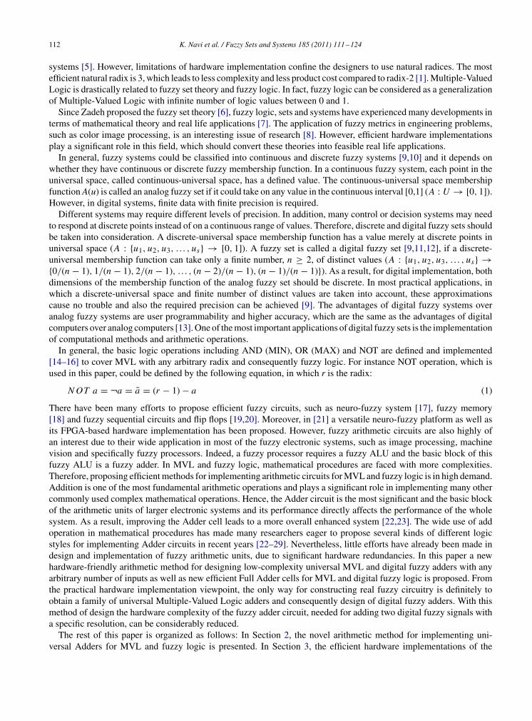
The general method for converting the arithmetic domain into the circuit level design is based on weighting and usingthreshold detector [29,30], which operates as a floor function. Fig. 1(a) shows the schematic of the Carry generatorblock. This block has k inputs with weights equal to one. The sum of the weighted input values is compared withTi threshold value. Ti adopts discrete values corresponding to (5) as follows:
Ti = r × i, i = 1, 2, . . . , r − 1 (17)
K. Navi et al. / Fuzzy Sets and Systems 185 (2011) 111–124 115
Fig. 1. Schematic of Adder cell, based on weighting blocks (a) Carry generator, (b) Sum generator.
The greatest i, whose corresponding Ti is less than or equal to the sum of the weighted input values, is considered asthe Carry output. For instance, for weighted sum equal to 2r + 1, Ti and Carry are 2r and 2, respectively. Choosingthese values for Ti enables the weighting block to implement the floor function in (5).
The schematic of the Sum generator block, corresponding to (9), is shown in Fig. 1(b). All of the inputs of this blockexcept Carry are weighted similar to Carry generator block and the Carry input is weighted to r. Valid values forSum output are 0, 1, 2, . . ., r − 1. Due to that, the valid values for the left side and hence for the right side of (9) arer2 − r, r2 − r + 1, . . ., r2 − 1. For generating Sum function, these values, except the first one, are chosen as thresholdSi , which means:
Si = r2 − r + i, i = 1, 2, . . . , r − 1 (18)
The greatest i, whose corresponding Si is less than or equal to the sum of the weighted input values, is considered asthe Sum output.
An important point for the radices higher than 2 is that the number of inputs of the Adder cell can be increasedaccording to the radix. Therefore, to obtain the maximum number of inputs, (2) can be generalized according to thefollowing equation, in which k denotes the number of inputs:
k∑j=1
in j = in1 + in2 + · · · + ink = Carry × r + Sum (19)
When each input adopts its maximum possible value, which is r − 1, the maximum possible value of the left side of(19) can be defined by the following equation, in which KMax denotes the maximum number of the permitted inputsand should be defined as follows:
MaxKMax∑j=1
in j = (r − 1)k (20)
By utilizing (20) in (2) and adopting the maximum values for Carry and Sum, KMax is obtained, which is r + 1.By choosing the obtained input values, all of the possible outputs are included and the Adder becomes faithful.
In the same manner as for unbalanced mode, according to (12) and (16), Ti and Si are determined for balanced modeas follows:
Ti = r × i −(
r − 1
2
), i = −r − 3
2, −r − 5
2, . . . , 0, . . . ,
r − 3
2,
r − 1
2(21)
Si = i, i = −r − 3
2, −r − 5
2, . . . , 0, . . . ,
r − 3
2,
r − 1
2(22)
In the hardware implementation, a margin equal to the half of the difference between two successive valid voltagelevels should be considered for all of the obtained thresholds and consequently all of the threshold values should bescaled down by this value.
116 K. Navi et al. / Fuzzy Sets and Systems 185 (2011) 111–124
3.1. Hardware implementation for MVL
Implementing the proposed method can be carried out in both voltage and current modes as well as for both balancedand unbalanced modes. However, due to the similarity between the methods of generating the Sum and Carry outputsin balanced and unbalanced modes, only the hardware implementation of the unbalanced mode is focused on voltageand current modes.
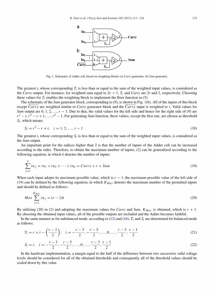
3.1.1. Voltage-mode circuit level realizationFig. 2(a) and (b) shows the voltage-mode implementation of the blocks, shown in Fig. 1(a) and (b), respectively.
These designs are based on the input capacitors [22] and standard MVL inverters (SMVLI). Standard MVL inverteris an MVL inverter which operates based on (1) and also restores the output voltage levels as a floor function. High-radix arithmetic circuits usually have higher number of transistors. However, this type of design leads to a significantreduction in the number of transistors. The capacitor network weights the inputs and the next SMVL inverter gate sensesthe desired threshold of the inputs. The standard MVL inverter in the Carry generator unit produces Carry instead ofCarry signal. Hence, another SMVLI gate is required for generating the Carry signal. As shown in Fig. 2(a), the inputsof the circuits are connected to the input node of SMVLI by means of the capacitor network. The capacitor networkperforms voltage division and determines the voltage of the input node of SMVLI based on the following equation:
VinSI, Carry =∑k
j=1 Vinj C j∑kj=1 C j
(23)
As the inputs of the Carry generator unit have the same weights, the capacitor values should be equal. Hence:
VinSMV L I, Carry = 1
k
k∑j=1
Vinj (24)
Because the sum of the input voltages is divided by k, the threshold levels of SMVLI in the Carry generator unit, whichare obtained by (17), should be divided by k. In the same manner, the input capacitors of the Sum generator unit are thesame, except the capacitor connected to the Carry input, which should be r times greater than the other capacitors.Therefore, VinSMV L ,Sum is obtained as follows:
VinSMV L I,Sum = 1
k + r
⎛⎝r × VCarry +
k∑j=1
Vinj
⎞⎠ (25)
Based on (18) and (25), the threshold levels in the Sum generator unit of Fig. 1(b) should be defined as (r2 − r + 1)/(k + r ), . . . , (r2 − 1)/(k + r ). The Sum generator unit of Fig. 2(b) generates Sum. Sum signal can be generated byutilizing another SMVLI gate in series with the existing one.
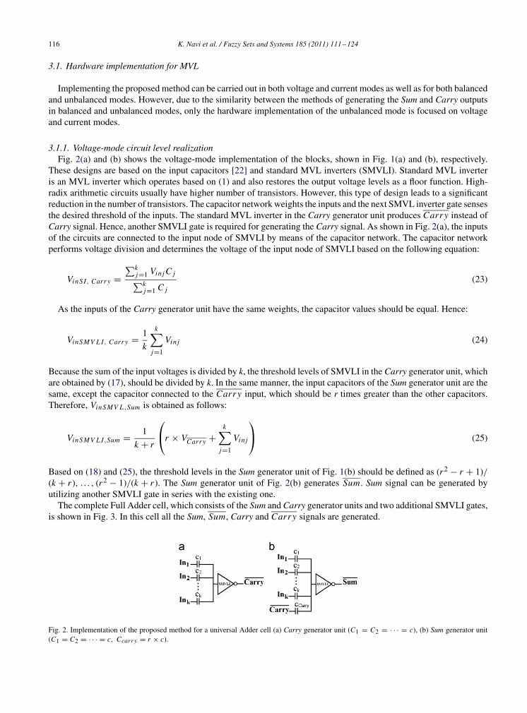
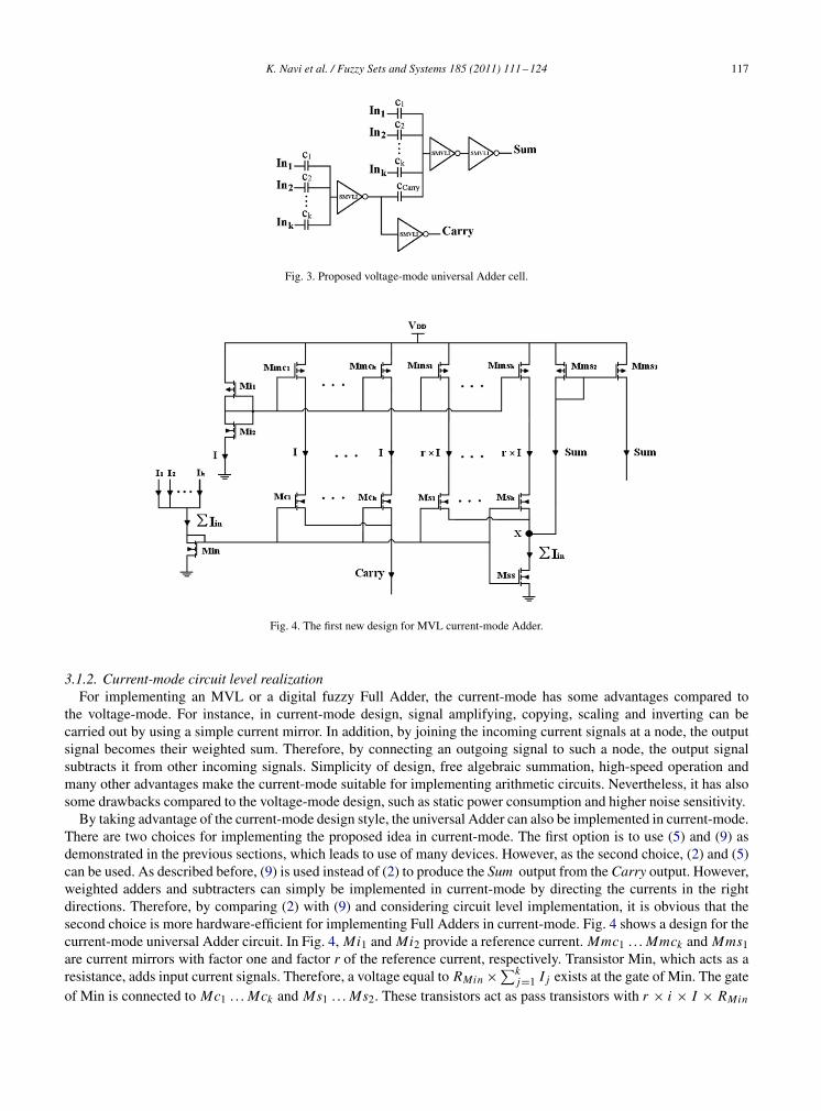
The complete Full Adder cell, which consists of the Sum and Carry generator units and two additional SMVLI gates,is shown in Fig. 3. In this cell all the Sum, Sum, Carry and Carry signals are generated.
Fig. 2. Implementation of the proposed method for a universal Adder cell (a) Carry generator unit (C1 = C2 = · · · = c), (b) Sum generator unit(C1 = C2 = · · · = c, Ccarr y = r × c).
K. Navi et al. / Fuzzy Sets and Systems 185 (2011) 111–124 117
Fig. 3. Proposed voltage-mode universal Adder cell.
Fig. 4. The first new design for MVL current-mode Adder.
3.1.2. Current-mode circuit level realizationFor implementing an MVL or a digital fuzzy Full Adder, the current-mode has some advantages compared to
the voltage-mode. For instance, in current-mode design, signal amplifying, copying, scaling and inverting can becarried out by using a simple current mirror. In addition, by joining the incoming current signals at a node, the outputsignal becomes their weighted sum. Therefore, by connecting an outgoing signal to such a node, the output signalsubtracts it from other incoming signals. Simplicity of design, free algebraic summation, high-speed operation andmany other advantages make the current-mode suitable for implementing arithmetic circuits. Nevertheless, it has alsosome drawbacks compared to the voltage-mode design, such as static power consumption and higher noise sensitivity.
By taking advantage of the current-mode design style, the universal Adder can also be implemented in current-mode.There are two choices for implementing the proposed idea in current-mode. The first option is to use (5) and (9) asdemonstrated in the previous sections, which leads to use of many devices. However, as the second choice, (2) and (5)can be used. As described before, (9) is used instead of (2) to produce the Sum output from the Carry output. However,weighted adders and subtracters can simply be implemented in current-mode by directing the currents in the rightdirections. Therefore, by comparing (2) with (9) and considering circuit level implementation, it is obvious that thesecond choice is more hardware-efficient for implementing Full Adders in current-mode. Fig. 4 shows a design for thecurrent-mode universal Adder circuit. In Fig. 4, Mi1 and Mi2 provide a reference current. Mmc1 . . . Mmck and Mms1are current mirrors with factor one and factor r of the reference current, respectively. Transistor Min, which acts as aresistance, adds input current signals. Therefore, a voltage equal to RMin ×∑k
j=1 I j exists at the gate of Min. The gateof Min is connected to Mc1 . . . Mck and Ms1 . . . Ms2. These transistors act as pass transistors with r × i × I × RMin
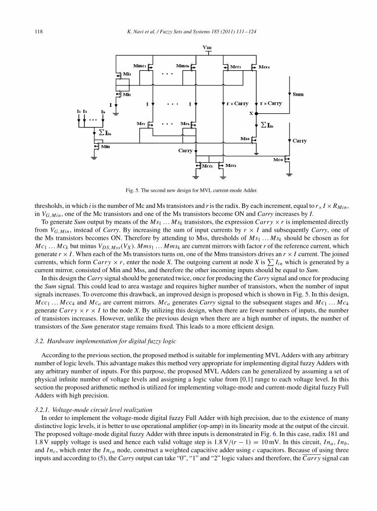
118 K. Navi et al. / Fuzzy Sets and Systems 185 (2011) 111–124
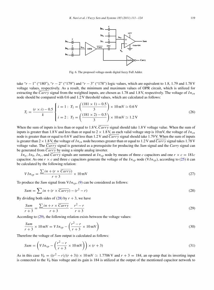
Fig. 5. The second new design for MVL current-mode Adder.
thresholds, in which i is the number of Mc and Ms transistors and r is the radix. By each increment, equal to r× I × RMin ,in VG,Min , one of the Mc transistors and one of the Ms transistors become ON and Carry increases by I.
To generate Sum output by means of the Ms1 . . . Msk transistors, the expression Carry × r is implemented directlyfrom VG,Min , instead of Carry. By increasing the sum of input currents by r × I and subsequently Carry, one ofthe Ms transistors becomes ON. Therefore by attending to Mss, thresholds of Ms1 . . . Msk should be chosen as forMc1 . . . Mck but minus VDS,Mss(VX ). Mms1 . . . Mmsk are current mirrors with factor r of the reference current, whichgenerate r × I . When each of the Ms transistors turns on, one of the Mms transistors drives an r × I current. The joinedcurrents, which form Carry × r , enter the node X. The outgoing current at node X is
∑Iin which is generated by a
current mirror, consisted of Min and Mss, and therefore the other incoming inputs should be equal to Sum.In this design the Carry signal should be generated twice, once for producing the Carry signal and once for producing
the Sum signal. This could lead to area wastage and requires higher number of transistors, when the number of inputsignals increases. To overcome this drawback, an improved design is proposed which is shown in Fig. 5. In this design,Mcc1 . . . Mcc4 and Mco are current mirrors. Mco generates Carry signal to the subsequent stages and Mc1 . . . Mc4generate Carry × r × I to the node X. By utilizing this design, when there are fewer numbers of inputs, the numberof transistors increases. However, unlike the previous design when there are a high number of inputs, the number oftransistors of the Sum generator stage remains fixed. This leads to a more efficient design.
3.2. Hardware implementation for digital fuzzy logic
According to the previous section, the proposed method is suitable for implementing MVL Adders with any arbitrarynumber of logic levels. This advantage makes this method very appropriate for implementing digital fuzzy Adders withany arbitrary number of inputs. For this purpose, the proposed MVL Adders can be generalized by assuming a set ofphysical infinite number of voltage levels and assigning a logic value from [0,1] range to each voltage level. In thissection the proposed arithmetic method is utilized for implementing voltage-mode and current-mode digital fuzzy FullAdders with high precision.
3.2.1. Voltage-mode circuit level realizationIn order to implement the voltage-mode digital fuzzy Full Adder with high precision, due to the existence of many
distinctive logic levels, it is better to use operational amplifier (op-amp) in its linearity mode at the output of the circuit.The proposed voltage-mode digital fuzzy Adder with three inputs is demonstrated in Fig. 6. In this case, radix 181 and1.8 V supply voltage is used and hence each valid voltage step is 1.8 V/(r − 1) = 10 mV. In this circuit, I na, I nb,and I nc, which enter the I ncn node, construct a weighted capacitive adder using c capacitors. Because of using threeinputs and according to (5), the Carry output can take “0”, “1” and “2” logic values and therefore, the Carry signal can
K. Navi et al. / Fuzzy Sets and Systems 185 (2011) 111–124 119
Fig. 6. The proposed voltage-mode digital fuzzy Full Adder.
take “r − 1” (“180”), “r − 2” (“179”) and “r − 3” (“178”) logic values, which are equivalent to 1.8, 1.79 and 1.78 Vvoltage values, respectively. As a result, the minimum and maximum values of OPR circuit, which is utilized forextracting the Carry signal from the weighted inputs, are chosen as 1.78 and 1.8 V, respectively. The voltage of I ncn
node should be compared with 0.6 and 1.2 V threshold values, which are calculated as follows:
Ti = (r × i) − 0.5
k
⎧⎪⎪⎨⎪⎪⎩
i = 1 : T1 =(
(181 × 1) − 0.5
3
)× 10 mV 0.6 V
i = 2 : T2 =(
(181 × 2) − 0.5
3
)× 10 mV 1.2 V
(26)
When the sum of inputs is less than or equal to 1.8 V, Carry signal should take 1.8 V voltage value. When the sum ofinputs is greater than 1.8 V and less than or equal to 2 × 1.8 V, as each valid voltage step is 10 mV, the voltage of I ncn
node is greater than or equal to 0.6 V and less than 1.2 V and Carry signal should take 1.79 V. When the sum of inputsis greater than 2×1.8 V, the voltage of I ncn node becomes greater than or equal to 1.2 V and Carry signal takes 1.78 Vvoltage value. The Carry signal is generated as a prerequisite for producing the Sum signal and the Carry signal canbe generated from Carry by using a simple analog inverter.
I na, I nb, I nc, and Carry signals are summed at I nsp node by means of three c capacitors and one r × c = 181ccapacitor. As one r × c and three c capacitors generate the voltage of the I nsp node (VI nsp), according to (25) it canbe calculated by the following relation:
V I nsp =∑
in + (r × Carry)
r + 3× 10 mV (27)
To produce the Sum signal from VI nsp, (9) can be considered as follows:
Sum =∑
in + (r × Carry) − (r2 − r ) (28)
By dividing both sides of (28) by r + 3, we have
Sum
r + 3=
∑in + r × Carry
r + 3− r2 − r
r + 3(29)
According to (29), the following relation exists between the voltage values:
Sum
r + 3× 10 mV = V I nsp −
(r2 − r
r + 3× 10 mV
)(30)
Therefore the voltage of Sum output is calculated as follows:
Sum =(
V I nsp −(
r2 − r
r + 3× 10 mV
))× (r + 3) (31)
As in this case Vb = ((r2 − r )/(r + 3)) × 10 mV 1.7706 V and r + 3 = 184, an op-amp that its inverting inputis connected to the Vb bias voltage and its gain is 184 is utilized at the output of the mentioned capacitor network to
120 K. Navi et al. / Fuzzy Sets and Systems 185 (2011) 111–124
Fig. 7. (a) The first proposed design of OPR circuit. (b) The second proposed design of OPR circuit.
Fig. 8. The proposed current-mode digital fuzzy Full Adder.
generate the Sum signal. It is worth mentioning that the bias voltage could be considered as 1.77 V for a more realisticcondition and manufacturability.
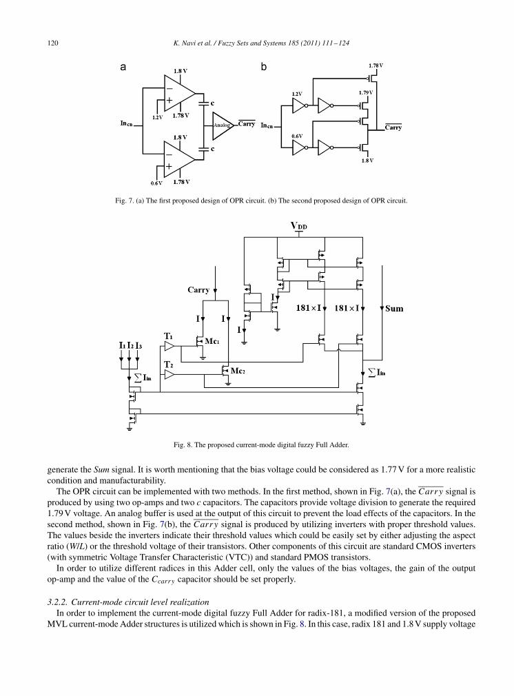
The OPR circuit can be implemented with two methods. In the first method, shown in Fig. 7(a), the Carry signal isproduced by using two op-amps and two c capacitors. The capacitors provide voltage division to generate the required1.79 V voltage. An analog buffer is used at the output of this circuit to prevent the load effects of the capacitors. In thesecond method, shown in Fig. 7(b), the Carry signal is produced by utilizing inverters with proper threshold values.The values beside the inverters indicate their threshold values which could be easily set by either adjusting the aspectratio (W/L) or the threshold voltage of their transistors. Other components of this circuit are standard CMOS inverters(with symmetric Voltage Transfer Characteristic (VTC)) and standard PMOS transistors.
In order to utilize different radices in this Adder cell, only the values of the bias voltages, the gain of the outputop-amp and the value of the Ccarry capacitor should be set properly.
3.2.2. Current-mode circuit level realizationIn order to implement the current-mode digital fuzzy Full Adder for radix-181, a modified version of the proposed
MVL current-mode Adder structures is utilized which is shown in Fig. 8. In this case, radix 181 and 1.8 V supply voltage
K. Navi et al. / Fuzzy Sets and Systems 185 (2011) 111–124 121
are used and the minimum and maximum current levels are chosen to be 0 A and 1.8 �A, respectively. Accordingly,each current step is 10 nA. By using three inputs in this circuit, according to (5), Carry output can take “0”, “1” and“2” logic values, which are equivalent to 0 A, 10 nA, and 20 nA current values, respectively.
Due to the existence of large number of logic levels, very high precision is needed in this case. Therefore, twoseparate threshold detector blocks with proper threshold values, T1 and T2, are utilized instead of setting the aspectratio (W/L) and the threshold voltage values of Mc1 and Mc2 transistors. As a matter of fact, T1 and T2 are the voltages,which appear at the input node of the threshold detector blocks, when the input current reaches 181× I and 2×181× I ,respectively.
4. Experimental results
In this section the operation of the proposed designs is tested for MVL and fuzzy logic. As the ternary logic hasthe most efficiency among the other logics and leads to less complexity [1], radix-3 is used to simulate the proposed
Table 1Truth table of the ternary Full Adder.
∑in Carry Carry 3 × Carry
∑in + 3 × Carry Sum Sum
0 0 2 6 6 0 21 0 2 6 7 1 12 0 2 6 8 2 03 1 1 3 6 0 24 1 1 3 7 1 15 1 1 3 8 2 06 2 0 0 6 0 2
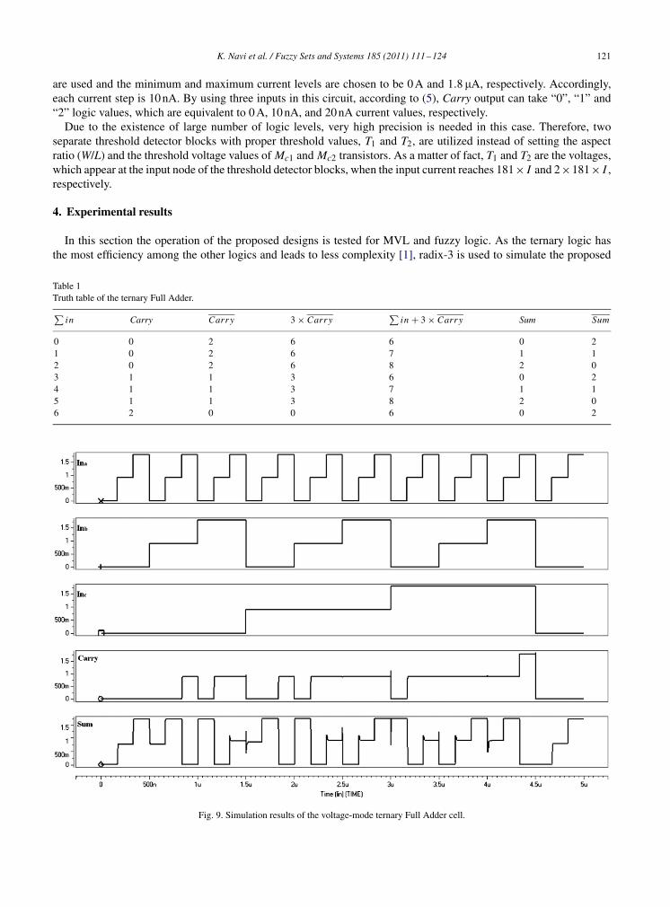
Fig. 9. Simulation results of the voltage-mode ternary Full Adder cell.
122 K. Navi et al. / Fuzzy Sets and Systems 185 (2011) 111–124
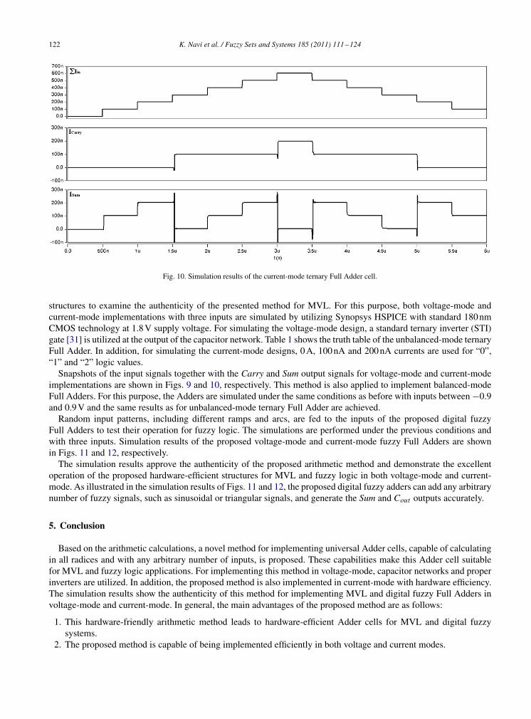
Fig. 10. Simulation results of the current-mode ternary Full Adder cell.
structures to examine the authenticity of the presented method for MVL. For this purpose, both voltage-mode andcurrent-mode implementations with three inputs are simulated by utilizing Synopsys HSPICE with standard 180 nmCMOS technology at 1.8 V supply voltage. For simulating the voltage-mode design, a standard ternary inverter (STI)gate [31] is utilized at the output of the capacitor network. Table 1 shows the truth table of the unbalanced-mode ternaryFull Adder. In addition, for simulating the current-mode designs, 0 A, 100 nA and 200 nA currents are used for “0”,“1” and “2” logic values.
Snapshots of the input signals together with the Carry and Sum output signals for voltage-mode and current-modeimplementations are shown in Figs. 9 and 10, respectively. This method is also applied to implement balanced-modeFull Adders. For this purpose, the Adders are simulated under the same conditions as before with inputs between −0.9and 0.9 V and the same results as for unbalanced-mode ternary Full Adder are achieved.
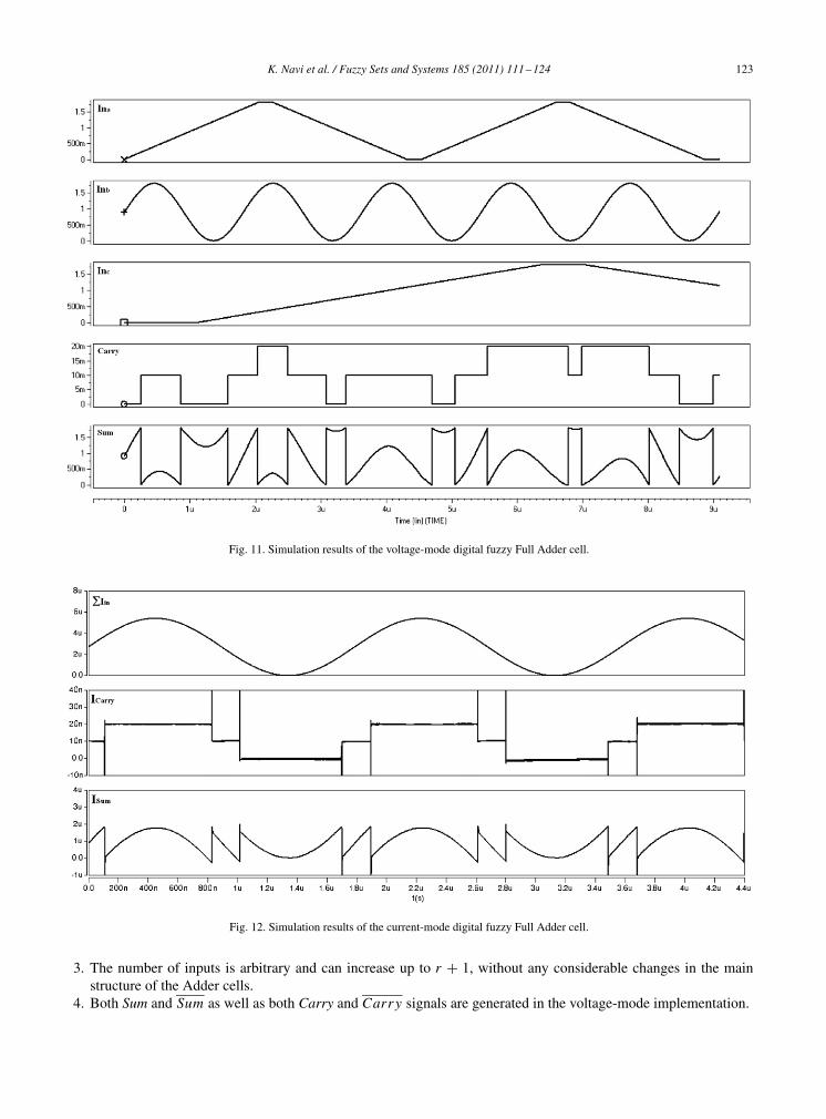
Random input patterns, including different ramps and arcs, are fed to the inputs of the proposed digital fuzzyFull Adders to test their operation for fuzzy logic. The simulations are performed under the previous conditions andwith three inputs. Simulation results of the proposed voltage-mode and current-mode fuzzy Full Adders are shownin Figs. 11 and 12, respectively.
The simulation results approve the authenticity of the proposed arithmetic method and demonstrate the excellentoperation of the proposed hardware-efficient structures for MVL and fuzzy logic in both voltage-mode and current-mode. As illustrated in the simulation results of Figs. 11 and 12, the proposed digital fuzzy adders can add any arbitrarynumber of fuzzy signals, such as sinusoidal or triangular signals, and generate the Sum and Cout outputs accurately.
5. Conclusion
Based on the arithmetic calculations, a novel method for implementing universal Adder cells, capable of calculatingin all radices and with any arbitrary number of inputs, is proposed. These capabilities make this Adder cell suitablefor MVL and fuzzy logic applications. For implementing this method in voltage-mode, capacitor networks and properinverters are utilized. In addition, the proposed method is also implemented in current-mode with hardware efficiency.The simulation results show the authenticity of this method for implementing MVL and digital fuzzy Full Adders involtage-mode and current-mode. In general, the main advantages of the proposed method are as follows:
1. This hardware-friendly arithmetic method leads to hardware-efficient Adder cells for MVL and digital fuzzysystems.
2. The proposed method is capable of being implemented efficiently in both voltage and current modes.
K. Navi et al. / Fuzzy Sets and Systems 185 (2011) 111–124 123
Fig. 11. Simulation results of the voltage-mode digital fuzzy Full Adder cell.
Fig. 12. Simulation results of the current-mode digital fuzzy Full Adder cell.
3. The number of inputs is arbitrary and can increase up to r + 1, without any considerable changes in the mainstructure of the Adder cells.
4. Both Sum and Sum as well as both Carry and Carry signals are generated in the voltage-mode implementation.

124 K. Navi et al. / Fuzzy Sets and Systems 185 (2011) 111–124
5. Using balanced or unbalanced mode inputs make no limitation on the proposed structures and only the thresholdvalues of the inverters should be correctly defined in the voltage-mode.
Acknowledgment
The authors would like to thank Dr. Belmond Yoberd for his literature contribution and are very grateful to theknowledgeable anonymous reviewers for their delicate comments and valuable suggestions which have improved thequality of the paper.
References
[1] S.L. Hurst, Multiple-Valued Logic—its status and its future, IEEE Trans. Comput. 33 (12) (1984) 1160–1179.[2] E. Dubrova, Multiple-Valued Logic in VLSI: challenges and opportunities, in: Proceedings of NORCHIP Conference, Oslo, Norway, November
1999, pp. 340–350.[3] K. Ozawa, T. Niimura, T. Nakashima, Fuzzy time-series model of electric power consumption, in: Proceedings of the IEEE Canadian Conference
on Electrical and Computer Engineering, vol. 2, May 1999, pp. 1195–1198.[4] Y.-Q. Yao, J.-S. Mi, Z.-J. Li, Attribute reduction based on generalized fuzzy evidence theory in fuzzy decision systems, Fuzzy Sets Syst.
170 (1) (2011) 64–75.[5] Z.G. Vranesic, V.C. Hamacher, Ternary logic in parallel multipliers, Comput. J. 15 (3) (1972) 254–258.[6] L.A. Zadeh, Fuzzy sets, Inf. Control 8 (3) (1965) 338–353.[7] L.T. Koczy, R. Lovassy, Fuzzy flip-flops and neural nets? in: Proceedings of the IEEE International Conference on Fuzzy Systems, London,
UK, July 2007, pp. 1–6.[8] V. Gregori, S. Morillas, A. Sapena, Examples of fuzzy metrics and applications, Fuzzy Sets Syst. 170 (1) (2011) 95–111.[9] M.S. Stachowicz, L. Beall, Fuzzy Logic, Wolfram Research Inc., 2003.
[10] G. Wang, C.L. Wen, A new fuzzy arithmetic for discrete fuzzy numbers, in: Proceedings of the 4th International Conference on Fuzzy Systemsand Knowledge Discovery, Haikou, China, vol. 1, August 2007, pp. 52–56.
[11] A. Gabrielli, E. Gandolfi, A fast digital fuzzy processor, IEEE Micro 19 (1) (1999) 61–79.[12] M.J. Patyra, J.L. Grantner, K. Koster, Digital fuzzy logic controller: design and implementation, IEEE Trans. Fuzzy Syst. 4 (4) (1996)
439–459.[13] J.Y. Han, S. Singh, Fast digital fuzzy operation units using comparison look-ahead, in: Proceedings of the 33rd Midwest Symposium on Circuits
and Systems, Calgary, Canada, vol. 2, August 1990, pp. 870–873.[14] H. Peyravi, A. Khoei, K. Hadidi, Design of an analog CMOS fuzzy logic controller chip, Fuzzy Sets Syst. 123 (2) (2002) 245–260.[15] T. Temel, A. Morgul, Implementation of multi-valued logic, simultaneous literal operations with full CMOS current-mode threshold circuits,
IEE Electron. Lett. 38 (4) (2002) 160–161.[16] A.M. Ibrahim, Fuzzy Logic for Embedded Systems Applications, Elsevier, 2004.[17] W.-Z. Wang, D.-M. Jin, Neuro-fuzzy system with high-speed low-power analog blocks, Fuzzy Sets Syst. 157 (22) (2006) 2974–2982.[18] K. Ozawa, K. Hirota, A VLSI design of fuzzy register, Inf. Sci. 71 (1–2) (1993) 203–221.[19] K. Ozawa, K. Hirota, L.T. Koczy, K. Omori, Algebraic fuzzy flip-flop circuits, Fuzzy Sets Syst. 39 (2) (1991) 215–226.[20] K. Hirota, W. Pedrycz, Designing sequential systems with fuzzy J-K flip-flops, Fuzzy Sets Syst. 39 (3) (1991) 261–278.[21] A.F. Gobi, W. Pedrycz, The potential of fuzzy neural networks in the realization of approximate reasoning engines, Fuzzy Sets Syst. 157 (22)
(2006) 2954–2973.[22] K. Navi, M.H. Moaiyeri, R. Faghih Mirzaee, O. Hashemipour, B. Mazloom Nezhad, Two new low-power full adders based on majority-not
gates, Microelectron. J. 40 (1) (2009) 126–130.[23] S. Goel, A. Kumar, M.A. Bayoumi, Design of robust, energy-efficient Full Adders for deep-submicrometer design using hybrid-CMOS logic
style, IEEE Trans. VLSI Syst. 14 (12) (2006) 1309–1321.[24] M.H. Moaiyeri, R. Faghih Mirzaee, K. Navi, T. Nikoubin, O. Kavehei, Novel direct designs for 3-input XOR function for low-power and
high-speed applications, Int. J. Electron. 97 (6) (2010) 647–662.[25] K. Navi, R. Faghih Mirzaee, M.H. Moaiyeri, B. Mazloom Nezhad, O. Hashemipour, K. Shams, Ultra high speed Full Adders, IEICE, Electron.
Express 5 (18) (2008) 744–749.[26] K. Navi, H. Hossein Sajedi, R. Faghih Mirzaee, M.H. Moaiyeri, A. Jalali, O. Kavehei, High-speed Full Adder based on minority function and
bridge style for nanoscale, Integrat. VLSI J. 44 (3) (2011) 155–162.[27] A.M. Shams, T.K. Darwish, M.A. Bayoumi, Performance analysis of low-power 1-bit CMOS Full Adder cells, IEEE Trans. VLSI Syst. 10 (1)
(2002) 20–29.[28] K. Navi, R. Farazkish, S. Sayedsalehi, M. Rahimi Azghadi, A new quantum-dot cellular automata full-adder, Microelectron. J. 41 (12) (2010)
820–826.[29] K. Navi, A. Kazeminejad, D. Etiemble, Performance of CMOS current mode Full Adders, in: Proceedings of the 24th International Symposium
on Multiple-Valued Logic, Boston, MA, May 1994, pp. 27–34.[30] N. Ikoma, K. Ozawa, K. Hirota, W. Pedrycz, Fuzzy sequential circuit based on weight-added fuzzy flip-flop, in: Proceedings of the 3rd IEEE
Conference on Fuzzy Systems, vol. 1, June 1994, pp. 291–296.[31] H.T. Mouftah, K.C. Smith, Injected voltage low-power CMOS for 3-valued logic, IEE Proc. G Electron. Circuit Syst. 129 (6) (1982) 270–272.
Related Documents