A graphene-based large area surface-conduction electron emission display Wei Lei a, * , Chi Li a,b , Matthew T. Cole b , Ke Qu a , Shuyi Ding a , Yan Zhang b , Jamie H. Warner c , Xiaobing Zhang a , Baoping Wang a , William I. Milne b,d a Display Research Centre, School of Electronic Science and Engineering, Southeast University, Nanjing 210096, PR China b Department of Engineering, Electrical Engineering Division, University of Cambridge, 9 JJ Thomson Avenue, CB3 0FA Cambridge, United Kingdom c Department of Materials, University of Oxford, Parks Road, Oxford OX1 3PH, United Kingdom d Department of Information Display, Kyung Hee University, Seoul 130-701, Republic of Korea ARTICLE INFO Article history: Received 18 October 2012 Accepted 6 January 2013 Available online 16 January 2013 ABSTRACT The fabrication and functionality of a 21 cm graphene-based transverse electron emission display panel is presented. A screen-printed triode edge electron emission geometry has been developed based on chemical vapor deposited (CVD) graphene supported on vertically aligned carbon nanotubes (CNT) necessary to minimize electrostatic shielding induced by the proximal bulk substrate. Integrated ZnO tetrapod electron scatterers have been shown to increase the emission efficiency by more than 90%. Simulated electron trajectories val- idate the observed emission characteristics with driving voltages less than 60 V. Fabricated display panels have shown real-time video capabilities that are hysteresis free (<0.2%), have extremely stable lifetimes (<3% variation over 10 h continuous operation) in addition to rapid temporal responses (<1 ms). Ó 2013 Elsevier Ltd. All rights reserved. 1. Introduction The outstanding electrical [1], mechanical [2,3], and chemi- cal [4,5] properties of low-dimensional nanocarbons, in par- ticular graphene and carbon nanotubes (CNT), make them attractive materials for next-generation transparent elec- trodes in state-of-the-art display technologies [6–8]. Graph- ene and CNTs have simultaneously high electrical and optical conductivities with near-zero band gaps [9–11]. The atomic thickness of graphene endows it with an exception- ally high aspect ratio, potentially higher even than CNTs, whilst defective edge terminations rich in dangling bonds render graphene superior to CNTs for highly efficient elec- tron tunneling [12], both of which qualifies graphene as a striking candidate for a variety of field emission applications. Linear dispersion in graphene gives rise to consequent massless fermions and in the presence of an electric field this allows field emission liberated electrons to avoid all backscat- tering as their escape velocity is independent of their energy. As such, graphene and many other graphitic nanocarbons are some of the best field emitting electron sources available to date. Recently many reports on field emission from graphene have emerged [7,8,12–14]. Pristine exfoliated graphene sheets have shown turn-on electric fields as low as 0.1 V lm 1 [12,15– 17]. Homogeneous, single-layer graphene deposited by electrophoresis has similarly demonstrated excellent field- emission properties such as turn on electric fields from 2.3 V lm 1 and field enhancement factors of up to 3700 [12,13]. Threshold fields of 1.5 V lm 1 with field enhance- ment factors in excess of 4500 have also been reported from screen printed graphene films [7]. Graphene field emitting 0008-6223/$ - see front matter Ó 2013 Elsevier Ltd. All rights reserved. http://dx.doi.org/10.1016/j.carbon.2013.01.004 * Corresponding author. E-mail address: [email protected] (W. Lei). CARBON 56 (2013) 255 – 263 Available at www.sciencedirect.com journal homepage: www.elsevier.com/locate/carbon

Welcome message from author
This document is posted to help you gain knowledge. Please leave a comment to let me know what you think about it! Share it to your friends and learn new things together.
Transcript
C A R B O N 5 6 ( 2 0 1 3 ) 2 5 5 – 2 6 3
.sc ienced i rec t .com
Avai lab le a t wwwjournal homepage: www.elsevier .com/ locate /carbon
A graphene-based large area surface-conduction electronemission display
Wei Lei a,*, Chi Li a,b, Matthew T. Cole b, Ke Qu a, Shuyi Ding a, Yan Zhang b,Jamie H. Warner c, Xiaobing Zhang a, Baoping Wang a, William I. Milne b,d
a Display Research Centre, School of Electronic Science and Engineering, Southeast University, Nanjing 210096, PR Chinab Department of Engineering, Electrical Engineering Division, University of Cambridge, 9 JJ Thomson Avenue, CB3 0FA Cambridge,
United Kingdomc Department of Materials, University of Oxford, Parks Road, Oxford OX1 3PH, United Kingdomd Department of Information Display, Kyung Hee University, Seoul 130-701, Republic of Korea
A R T I C L E I N F O
Article history:
Received 18 October 2012
Accepted 6 January 2013
Available online 16 January 2013
0008-6223/$ - see front matter � 2013 Elsevihttp://dx.doi.org/10.1016/j.carbon.2013.01.004
* Corresponding author.E-mail address: [email protected] (W. Lei).
A B S T R A C T
The fabrication and functionality of a 21 cm graphene-based transverse electron emission
display panel is presented. A screen-printed triode edge electron emission geometry has
been developed based on chemical vapor deposited (CVD) graphene supported on vertically
aligned carbon nanotubes (CNT) necessary to minimize electrostatic shielding induced by
the proximal bulk substrate. Integrated ZnO tetrapod electron scatterers have been shown
to increase the emission efficiency by more than 90%. Simulated electron trajectories val-
idate the observed emission characteristics with driving voltages less than 60 V. Fabricated
display panels have shown real-time video capabilities that are hysteresis free (<0.2%), have
extremely stable lifetimes (<3% variation over 10 h continuous operation) in addition to
rapid temporal responses (<1 ms).
� 2013 Elsevier Ltd. All rights reserved.
1. Introduction
The outstanding electrical [1], mechanical [2,3], and chemi-
cal [4,5] properties of low-dimensional nanocarbons, in par-
ticular graphene and carbon nanotubes (CNT), make them
attractive materials for next-generation transparent elec-
trodes in state-of-the-art display technologies [6–8]. Graph-
ene and CNTs have simultaneously high electrical and
optical conductivities with near-zero band gaps [9–11]. The
atomic thickness of graphene endows it with an exception-
ally high aspect ratio, potentially higher even than CNTs,
whilst defective edge terminations rich in dangling bonds
render graphene superior to CNTs for highly efficient elec-
tron tunneling [12], both of which qualifies graphene as a
striking candidate for a variety of field emission
applications.
er Ltd. All rights reserved
Linear dispersion in graphene gives rise to consequent
massless fermions and in the presence of an electric field this
allows field emission liberated electrons to avoid all backscat-
tering as their escape velocity is independent of their energy.
As such, graphene and many other graphitic nanocarbons are
some of the best field emitting electron sources available to
date. Recently many reports on field emission from graphene
have emerged [7,8,12–14]. Pristine exfoliated graphene sheets
have shown turn-on electric fields as low as 0.1 V lm�1 [12,15–
17]. Homogeneous, single-layer graphene deposited by
electrophoresis has similarly demonstrated excellent field-
emission properties such as turn on electric fields from
2.3 V lm�1 and field enhancement factors of up to 3700
[12,13]. Threshold fields of �1.5 V lm�1 with field enhance-
ment factors in excess of 4500 have also been reported from
screen printed graphene films [7]. Graphene field emitting
.
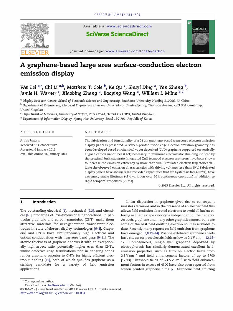
Fig. 1 – (a) Fabrication of the graphene edge field emission structure; (i) Screen printed Ag (2 lm) bottom cathode on a glass
substrate (3 mm). (ii) Screen printed 50 lm SiO2 dielectric and subsequent buffered hydro fluoric acid wet etching for via
formation. (iii) Screen printed Ag (2 lm) gate and top cathode. (iv) Chemical vapor deposition of Ni catalyzed vertically aligned
carbon nanotubes directly onto the gate and cathode. (v) Graphene transferred onto the CNT arrays. (vi) Screen-printing of the
ZnO tetrapod electron scatterers between the gate and top cathode. (b) Cross-section schematic of the display. The electrodes
forming the triode structure are the Ag gate, the Ag top cathode and the phosphor/ITO/glass anode which are separated from
the glass gate-cathode substrate by 3 mm ceramic spacers. (c) A scanning electron micrograph (false colored) of a complete
graphene edge emission structure showing the gate and cathode (cath.) electrodes, as well as the ZnO tetrapod electron
scatterers (Scale bar: 200 lm). (d) A scanning electron micrograph (false colored) of a single ZnO tetrapod and graphene edge
(Scale bar: 5 lm). (e) A cross-section scanning electron micrograph (false colored) of the cathode, as indicated by the dashed
line in (c), showing the graphene edge emitter supported by an array of CNT bundles (Scale bar: 1 lm). Note that the cross-
section of the gate electrode has an equivalent structure.
256 C A R B O N 5 6 ( 2 0 1 3 ) 2 5 5 – 2 6 3
arrays on Cu foil, fabricated by conventional photolithogra-
phy and wet etching techniques, offer one possible route to
micron-scale planar emitters over large areas, though such
structures offer relatively poor turn-on fields (�7.2 V lm�1
[8]). Impressive emission stability and uniformity, signifi-
cantly better than graphene-powders and comparable to
CNTs, have also been demonstrated [12]. Nevertheless, such
solution-based graphene deposition results in flakes that are
oriented at various uncontrolled and irreproducible angles
relative to the substrate, making such approaches largely
non-scalable.
Though the lateral size to thickness ratio of graphene is
exceptionally large, in order to fully exploit this field
enhancement in traditional vertical emitter geometries the
graphene must stand on edge rather than lay in-plane on
the substrate, as such morphologies offer comparatively
poor emission performance [18]. However, obtaining verti-
cally aligned graphene sheets is currently challenging.
Microwave plasma chemical vapor deposition has been
used elsewhere to synthesize promising carbon nanowall
field emitters [19,20]. Nevertheless, almost all reports on
in situ and ex situ graphene growth, exfoliation, and deposi-
tion techniques have thus far yielded flat sheets lying adja-
cent to, and in intimate contact with their substrate.
Although an improvement in field emission performance
has certainly been observed [13] – a consequence of lattice
defects and free edge-bond formation induced by chemical
and thermal post treatments – such emitters are difficult
to integrate into practical displays due to their poor topo-
graphic uniformity and emission reproducibility. Exploiting
the lateral, in-plane emission properties of graphene is per-
haps the most scalable route to the eventual integration of
graphene into field emission systems, especially following
the recent advancements in ultra-large-area CVD graphene
single crystal growth [21]. Despite this, to fully realise the
maximum field enhancement the graphene edge emitters
must be supported above the proximal bulk substrate to en-
sure negligible substrate-induced electrostatic shielding [22].
Herein, we report a new graphene-based transverse field
emission structure employing graphene edge emitters sup-
ported on arrays of CNTs with integrated electron scattering
ZnO tetrapods.

Fig. 2 – Graphene and CNTs by thermal chemical vapor deposition. Raman spectra (at 457 nm (blue), 532 nm (green) and
633 nm (red) excitation) of; (a) CNTs and (b) graphene (Gr). (c) ID/IG and I2D/IG distributions for the graphene edge emitter and
CNT supports (532 nm excitation). (d) Graphene and CNT dispersion relation for ID/IG (grey), I2D/IG (green) and Raman shift of
the D (j), G (d) and 2D (m) peaks. (e) A scanning electron micrograph of a graphene film (Scale bar: 2 lm) and (f) the
corresponding ID/IG map (Scale bar: 2 lm), both highlighting the uniformity of the graphene. More than 95% of the graphene is
few layer graphene (FLG), as determined from I2D/IG data (not shown). (For interpretation of the references to color in this
figure legend, the reader is referred to the web version of this article.)
C A R B O N 5 6 ( 2 0 1 3 ) 2 5 5 – 2 6 3 257
The graphene edge electron emitter is a planar triode
where the cathode and gate electrodes align orthogonally.
To passivate the substrate induced electric field shielding
[23] CNT arrays (1.5 lm height/0.2 lm bundle diameter/2 lm
pitch) were employed to mechanically elevate and electrically
connect to the graphene electron emitter (Fig. 2b). The emis-
sion performance was dramatically enhanced by employing
secondary and back-scattered electron sites formed from
ZnO. ZnO was selected as it has a high secondary electron
yield of 2.3 [24], has a wide variety of morphologies that are
solution processable, and can be synthesized inexpensively
at low temperatures. ZnO nanowires and nanorods showed
inferior performance compared to ZnO tetrapods. The one
dimensional ZnO nanowires and nanorods were more com-
pact and tended to aggregate more readily resulting in denser
films with significantly less scattering capabilities. Moreover,
the nanowires and nanorods often aligned parallel to the sub-
strate and the field enhancement associated with their geom-
etry was not fully realized. In contrast the morphology of the
tetrapods ensured that at least a single axis offered zones of
high field enhancement.
2. Experimental
2.1. Display fabrication
The fabrication process of the edge emission triode is detailed
in Fig. 1a. Glass substrates were screen printed with a bottom
cathode (Ag, 2 lm), an SiO2 dielectric layer, top cathode (Ag,
2 lm), and gate electrode (Ag, 2 lm). The 50 lm screen printed
SiO2 dielectric suspension separates the cathode and gate. Ar-
rays of vias were etched in the dielectric using buffered
hydrofluoric acid such that the cathode is in plane with the
gate electrode. The cathode and gate were subsequently mag-
netron sputtered with Ni dots to catalyse CNT growth, as de-
scribed below. Panels were then coated with graphene
supported on an SU-8 mediator. The edge electron emitter
was then patterned by photolithography directly on the
graphene/SU-8. Finally, graphene was patterned by oxygen
reactive ion etching (20 W, 30 s). A typical completed device
is shown in Fig. 1c.
2.1.1. CNT, graphene, and ZnO tetrapod synthesis2.1.1.1. Carbon nanotubes. CNTs were grown from d.c. mag-
netron sputtered Ni catalysts (15 nm, 99.99%, Beijing Zhongj-
ingkeyi Technology Co., Ltd.) on Ag-coated glass cathodes
patterned using conventional photolithography. Vertically
aligned multi-walled CNT bundles were synthesized by ther-
mal chemical vapor deposition (CVD) in a commercially avail-
able cold-wall reactor (Black Magic, Aixtron Ltd.). Catalyst
samples were annealed in Ar (Grade 4.0) at 420 �C (5 �C s�1)
for 40 s with subsequent exposure to C2H2 (200 sccm, Grade
4.0) in a NH3 ballast (50 sccm, Grade 4.0) at 450 �C and
1.4 · 103 Pa. Following a 60 s growth the multi-walled CNTs
were 10.0 ± 0.6 (±1 S.D.) lm in length and 50 ± 2 (±1 S.D.) nm
in diameter.

Fig. 3 – ZnO tetrapod electron scatterers synthesized by non-
catalytic vapor phase transport. (a) X-ray diffraction pattern
of the as-synthesized ZnO tetrapods. Inset: High-resolution
electron micrograph and the corresponding select area
diffraction pattern showing the regular wurtzite crystal
structure (Scale bar: 2 nm) with a lattice constant of
0.32 ± 0.03 nm. (b) Energy dispersive X-ray spectrum
highlighting the stoichiometry of the synthesized ZnO
tetrapods. Inset: Scanning electron micrograph of as-
synthesized ZnO tetrapods (Scale bar: 20 lm). (c) UV–Vis
spectrum showing a Tauc gap of 3.68 eV.
258 C A R B O N 5 6 ( 2 0 1 3 ) 2 5 5 – 2 6 3
2.1.1.2. Graphene. Graphene was synthesized in a custom-
built thermal CVD tube furnace. Cu catalysts (foil, 99.99%, Bei-
jing Zhongjingkeyi Technology Co., Ltd.) were heated to
1000 �C (4 �C s�1) and exposed to CH4 (40 sccm, Grade 4.0)
and H2 (40 sccm, Grade 4.0) at 100 Pa. Pristine graphene was
transferred to the supporting CNT arrays (cathode) using an
SU-8 (2000, MicroChem Corp.) mediator and wet-etching of
the underlying Cu (aqueous FeCl3 (25 wt.%), Nanjing Chemical
Solution Corp.) [25,26]. SU-8 was removed by dissolution in
acetone.
2.1.1.3. ZnO tetrapods. ZnO tetrapods were synthesized by
non-catalytic vapor phase transport of Ar (200 sccm, Grade
4.0) and O2 (100 sccm, Grade 4.0) at 104 Pa in a custom-built
horizontal tube furnace operated at 900 �C (4 �C s�1). The
ZnO tetrapods were collected and mixed with ethyl cellulose
ethoce terpineol. A 10 lm thick film was subsequently
screen-printed (NewLong Seimitsu) between the cathode
and gate using this paste.
2.2. Materials characterization
2.2.1. CNTs and grapheneFig. 2a and b show the Raman spectra of the CNTs and graph-
ene, respectively, acquired at 457 nm (blue), 532 nm (green),
and 633 nm (red) excitations. Fig. 2e and f show a scanning
electron micrograph and the corresponding Raman intensity
ratio of the D and G peaks (ID/IG) spatially resolved (532 nm),
highlighting the uniformity of the CVD-deposited graphene.
The graphene is >95% few layer graphene with an ID/
IG = 0.21 ± 0.09 and I2D/IG = 0.30 ± 0.07 (±1 S.D.) (Fig. 2b) [27].
The asymmetric fourfold Lorentzian-fitted 2D peak
(2704 cm�1) of the graphene has a full-width half-maximum
of �51.8 cm�1, suggesting the presence of highly graphitic tur-
bostratic strata [28,29]. The CNTs are multi-walled and have
an ID/IG = 0.21 ± 0.03 and I2D/IG = 0.41 ± 0.05 (±1 S.D.) (Fig. 2b
and c). The CNTs (and graphene) have D, G and 2D peak dis-
persions of 0.235 (0.026) cm�1 nm�1, 0.062 (0.025) cm�1 nm�1,
and 0.480 (0.305) cm�1 nm�1 (Fig. 2d), respectively, consistent
with high quality graphitic CVD nanocarbons [29].
2.2.2. ZnO tetrapodsFig. 3a shows an X-ray diffraction (XRD) pattern from the as-
synthesized ZnO tetrapods [30]. All diffraction peaks are
attributed to the ZnO hexagonal wurtzite crystal with lattice
constants of a = 3.249 A and c = 5.205 A – consistent with
JCPDS card No. 89-0511. High-resolution transmission elec-
tron microscopy and select-area electron diffractograms (In-
sets, Fig. 3a) confirm this, with a measured lattice constant
of 0.32 ± 0.03 nm and an approximate d-spacing of 0.28 nm.
No impurity diffraction peaks were detected. Energy disper-
sive X-ray spectroscopy corroborates this (Fig. 3b), evidencing
a Zn-rich O:Zn ratio of 1:3.47 [31]. The Tauc gap was estimated
to be 3.68 eV, further evidencing the high quality of the as-
synthesized ZnO tetrapods (Fig. 3c) [32].
2.2.3. TechniquesCNTs and graphene were analyzed using a polychromatic Ra-
man spectrometer (Renishaw InVia) fitted with fused-silica
optics and a piezo stage (nominal step size = 0.2 lm) with a
probe diameter of 1.2 lm and a 100· aperture. Excitation
sources at 457, 532, and 633 nm with incident powers
C A R B O N 5 6 ( 2 0 1 3 ) 2 5 5 – 2 6 3 259
<10 mW were used throughout. Triplicate accumulations and
a 20 s integration time where used to optimize the signal-to-
noise. Scanning electron micrographs were acquired using a
Quanta 20 FEI and a variable pressure Carl Zeiss Gemini-
Sigma scanning electron microscopes operated at 1 kV. An
aberration corrected FEI Titan3 80–300 in scanning mode with
bright-field and annular dark-field detectors, and a JEOL
JEM-4000 EX high-resolution transmission electron micro-
scope were employed to image the crystalline structure of
the ZnO tetrapods and to record the corresponding select area
diffraction patterns. X-ray diffraction measurements were
performed using an ARL X’TRA powder diffractometer
(Thermo Scientific) with an integrated Peltier cooled Si(Li)
solid state detector and a low-angle resolution down to 0.5o.
A UV–Vis (deuterium/tungsten) spectrophotometer (Thermo
Scientific), with a 2 nm spectral resolution and a beam size
of 1 cm2, was used for Tauc gap measurements.
2.3. Field emission measurements
Field emission measurements were performed using a cus-
tom-built turbo-molecular pumped chamber evacuated to
<10�4 Pa attached to computer controlled source-measure
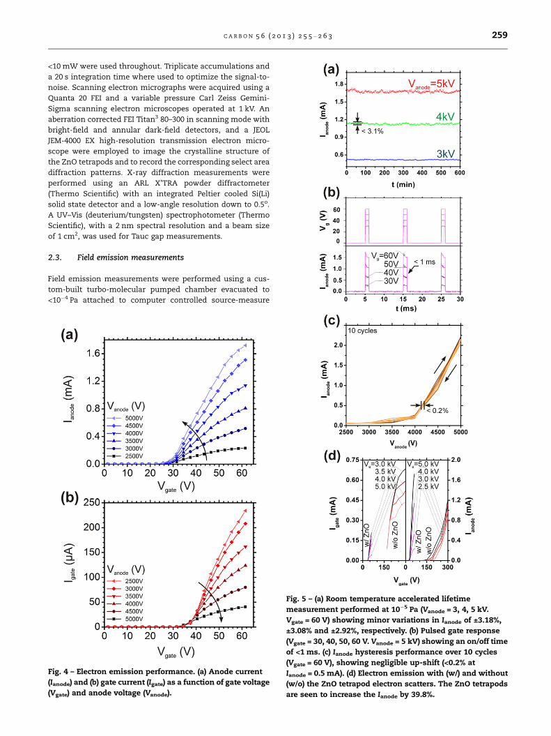
Fig. 4 – Electron emission performance. (a) Anode current
(Ianode) and (b) gate current (Igate) as a function of gate voltage
(Vgate) and anode voltage (Vanode).
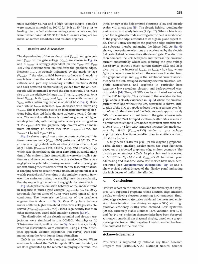
Fig. 5 – (a) Room temperature accelerated lifetime
measurement performed at 10�5 Pa (Vanode = 3, 4, 5 kV.
Vgate = 60 V) showing minor variations in Ianode of ±3.18%,
±3.08% and ±2.92%, respectively. (b) Pulsed gate response
(Vgate = 30, 40, 50, 60 V. Vanode = 5 kV) showing an on/off time
of <1 ms. (c) Ianode hysteresis performance over 10 cycles
(Vgate = 60 V), showing negligible up-shift (<0.2% at
Ianode = 0.5 mA). (d) Electron emission with (w/) and without
(w/o) the ZnO tetrapod electron scatters. The ZnO tetrapods
are seen to increase the Ianode by 39.8%.

Fig. 6 – (a) Simulated potential distribution (color bar, V) and electron trajectories (red curves) at the graphene edge, and (b) the
ZnO tetrapod electron scatter site. (c and d) Optical micrographs of a prototype 21 cm diagonal graphene electron emission
display. Inset: Optical micrograph of a 23 pixel · 11 pixel section of a fabricated display panel. (For interpretation of the
references to colour in this figure legend, the reader is referred to the web version of this article.)
260 C A R B O N 5 6 ( 2 0 1 3 ) 2 5 5 – 2 6 3
C A R B O N 5 6 ( 2 0 1 3 ) 2 5 5 – 2 6 3 261
units (Keithley 6517A) and a high voltage supply. Samples
were vacuum annealed at 500 �C for 24 h at 10�5 Pa prior to
loading into the field emission testing system where samples
were further baked at 180 �C for 24 h to ensure complete re-
moval of surface absorbates and residual organics.
3. Results and discussion
The dependencies of the anode current (Ianode) and gate cur-
rent (Igate) on the gate voltage (Vgate) are shown in Fig. 4a
and b. Ianode is strongly dependent on the Vgate. For Vgate
<30 V few electrons were emitted from the graphene edges.
However, Ianode is strongly influenced by the anode voltage
(Vanode). If the electric field between cathode and anode is
much less than the electric field established between the
cathode and gate any secondary emitted electrons (SEEs)
and back-scattered electrons (BSEs) yielded from the ZnO tet-
rapods will be attracted toward the gate electrode. This gives
rise to an unsatisfactorily large Igate. Thus, Ianode reduces. For a
fixed Vanode, both Ianode and Igate increase with increasing
Vgate, with a saturating response at about 60 V (Fig. 4). How-
ever, whilst Ianode increases, Igate decreases with increasing
Vanode. This is primarily due to an increasing number of elec-
trons being diverted from the gate trajectory toward the an-
ode. The emission efficiency is therefore greater at higher
anode potentials, with the highest efficiency occurring when
30 V < Vgate < 60 V. The graphene edge emitter offers a maxi-
mum efficiency of nearly 90% with Ianode = 1.2 mA, for
Vanode = 5 kV and Vgate = 60 V.
Fig. 5a shows typical room temperature accelerated life-
times measurements (Vgate = 60 V) performed at 10�5 Pa. The
emission is highly stable with variations in anode currents of
only ±3.18% (Vanode = 3 kV), ±3.08% (4 kV), and ±2.92% (5 kV),
which also demonstrates the near-zero burn-in/conditioning
time of the emitters. ZnO tetrapod films were electrically con-
tinuous and were connected to the gate electrode. There was
negligible charge build-upduring emission. Indeed, the negligi-
ble drift during the emission current lifetime test confirms this.
If charging were to occur it would undoubtedly manifest as a
weakly parabolic shift over time in the emission current. How-
ever, the emission during the stability tests was stochastic,
thereby supporting the notion of negligible charging effects.
Fig. 5b depicts the emission behavior of the anode current
in response to pulsed gate voltages (Vgate = 30, 40, 50, 60 V).
Extremely fast on times of <1 ms were noted under all gate
conditions. The hysteresis performance of the graphene
edge-emitter is shown in Fig. 5c. Over 10 cycles extremely
minor shifts to higher threshold extraction voltages was ob-
served (DVanode(Ianode = 0.5 mA) < 0.2%), significantly less than
other nanocarbon-based field emission sources [33,34].
The distribution of the electric potential and electron tra-
jectories were simulated in the COMSOL Multiphysics (V.
3.3A) environment, as illustrated in Fig. 6a and b, respectively.
Potential distributions were calculated using a finite differ-
ence approach. Electron trajectories (red curves) were esti-
mated using the Forth Runge Kutta formalism.
ZnO is an n-type wide band-gap semiconductor. When
electrons bombard the ZnO tetrapods SEEs are liberated, as
are BSEs generated by the reflected impinging electrons. The
initial energy of the field emitted electrons is low and linearly
scales with anode bias [35]. The electric field surrounding the
emitters is particularly intense (5 V lm�1). When a bias is ap-
plied to the gate electrode a strong electric field is established
at the graphene edge, attributed to its high in-plane aspect ra-
tio. The CNT array decouples the graphene edge-emitter from
the substrate thereby enhancing the fringe field. As Fig. 6b
shows, these primary electrons are accelerated by the electric
field established between the cathode and gate. The electrons
then bombard the ZnO tetrapods and increase the emission
current substantially whilst also reducing the gate voltage
necessary to extract a given current density. SEEs and BSEs
give rise to the increased Ianode, as Ianode = IGr + ISEE, where
IGr is the current associated with the electrons liberated from
the graphene edge and ISEE is the additional current associ-
ated with the ZnO tetrapod secondary electron emission. Gra-
phitic nanocarbons, and graphene in particular have
extremely low secondary electron and back-scattered elec-
tron yields [36]. Thus, all SEEs can be attributed exclusively
to the ZnO tetrapods. This increase in the available electron
population is clearly evidenced in Fig. 5d where the emission
current with and without the ZnO tetrapods is shown. Inte-
gration of the ZnO tetrapods reduces the gate current by a fac-
tor of two. In the absence of the ZnO tetrapods approximately
36% of the emission current leaks to the gate, whereas inte-
gration of the ZnO tetrapod electron scatter sites results in
a dramatic reduction to 2.4% under equivalent extraction con-
ditions (Vanode = 5 kV). ZnO tetrapods increase the anode cur-
rent by 39.8% (Vanode = 5 kV) under a gate voltage
approximately five times smaller than in emitters without
the ZnO tetrapods.
A fully sealed 320 · 240 pixel (21 cm diagonal) graphene-
based electron emission display panel has been fabricated
based on the reported graphene edge emitter geometry. The
display panel employs a ZnO: Zn phosphor and is operated
at 5 · 10�5 Pa, Vg = 60 V and Vanode = 5 kV. Individual pixel
addressing and real-time video rate movies have been dem-
onstrated (see Supplementary Information). Fig. 6c and d
show typical optical images of the display panel indicating
the high degree of uniformity afforded.
4. Conclusions
Here we report on the fabrication and functionality of a large-
area CNT-supported graphene triode electron edge emission
display employing electron scattering ZnO tetrapods. Simu-
lated edge electron trajectories validated the measured emis-
sion characteristics. Low driving voltages (<60 V) with high
emission efficiency (>90%) were obtained. Low hysteresis
(<0.2%), extremely stable lifetimes (<3% variation over 10 h)
and fast (<1 ms) emission characteristics have been observed.
A monochromatic 21 cm diagonal display, based on a graph-
ene edge electron emitter, capable of real-time video has been
demonstrated for the first time.
Acknowledgements
This work is supported by National Key Basic Research
Program 973 (2010CB327705), National Natural Science
262 C A R B O N 5 6 ( 2 0 1 3 ) 2 5 5 – 2 6 3
Foundation Project (51120125001, 51202027, 51002031,
61101023), China Postdoctoral Science Foundation
(2012M511648), Foundation of Doctoral Program of Ministry
of Education (20100092110015), and the Research Fund for
International Young Scientists from NSFC (51050110142).
The Authors’ thank the Cavendish Laboratory, Cambridge
University for the kind use of their Raman facilities. M.T.C
acknowledges St Edmund’s College Cambridge University
and the Isaac Newton Trust, Trinity College Cambridge
University, for generous financial support.
Appendix A. Supplementary data
Supplementary data associated with this article can be found,
in the online version, at http://dx.doi.org/10.1016/
j.carbon.2013.01.004.
R E F E R E N C E S
[1] Geim AK, Novoselov KS. The rise of graphene. Nat Mater2007;6(3):183–91.
[2] Lee C, Wei X, Kysar JW, Hone J. Measurement of the elasticproperties and intrinsic strength of monolayer graphene.Science 2008;321(5887):385–8.
[3] Bunch JS, Verbridge SS, Alden JS, van der Zande AM, ParpiaJM, Craighead HG, et al. Impermeable atomic membranesfrom graphene sheets. Nano Lett 2008;8(8):2458–62.
[4] Elias DC, Nair RR, Mohiuddin TMG, Morozov SV, Blake P,Halsall MP, et al. Control of graphene’s properties byreversible hydrogenation: evidence for graphane. Science2009;323(5914):610–3.
[5] Wang X, Li X, Zhang L, Yoon Y, Weber PK, Wang H, et al. N-doping of graphene through electrothermal reactions withammonia. Science 2009;324(5928):768–71.
[6] Bae S, Kim H, Lee Y, Xu XF, Park JS, Zheng Y, et al. Roll-to-rollproduction of 30-inch graphene films for transparentelectrodes. Nat Nanotechnol 2010;5(8):574–8.
[7] Qian M, Feng T, Ding H, Lin L, Li H, Chen Y, et al. Electron fieldemission from screen-printed graphene films.Nanotechnology 2009;20(42):425702.
[8] Huang C-K, Ou Y, Bie Y, Zhao Q, Yu D. Well-aligned graphenearrays for field emission displays. Appl Phys Lett2011;98(26):263104.
[9] Eda G, Fanchini G, Chhowalla M. Large-area ultrathin films ofreduced graphene oxide as a transparent and flexibleelectronic material. Nat Nanotechnol 2008;3(5):270–4.
[10] Tombros N, Jozsa C, Popinciuc M, Jonkman HT, van Wees BJ.Electronic spin transport and spin precession in singlegraphene layers at room temperature. Nature2007;448(7153):571–4.
[11] Novoselov KS, Geim AK, Morozov SV, Jiang D, Zhang Y,Dubonos SV, et al. Electric field effect in atomically thincarbon films. Science 2004;306(5696):666–9.
[12] Wu Z-S, Pei S, Ren W, Tang D, Gao L, Liu B, et al. Fieldemission of single-layer graphene films prepared byelectrophoretic deposition. Adv Mater 2009;21(17):1756–60.
[13] Dong J, Zeng B, Lan Y, Tian S, Shan Y, Liu X, et al. Fieldemission from few-layer graphene nanosheets produced byliquid phase exfoliation of graphite. J Nanosci Nanotechnol2010;10(8):5051–5.
[14] Tsai JTH, Chu TYE, Shiu J-Y, Yang C-S. Field emission from anindividual freestanding graphene edge. Small2012;8(24):3739–45.
[15] Lee SW, Lee SS, Yang E-H. A Study on field emissioncharacteristics of planar graphene layers obtained from ahighly oriented pyrolyzed graphite block. Nano Res Lett2009;4(10):1218–21.
[16] Wang HM, Zheng Z, Wang YY, Qiu JJ, Guo ZB, Shen ZX, et al.Fabrication of graphene nanogap with crystallographicallymatching edges and its electron emission properties. ApplPhys Lett 2010;96(2):023106.
[17] Yamaguchi H, Murakami K, Eda G, Fujita T, Guan P, Wang W,et al. Field emission from atomically thin edges of reducedgraphene oxide. ACS Nano 2011;5(6):4945–52.
[18] Xiao Z, She J, Deng S, Tang Z, Li Z, Lu J, et al. Field electronemission characteristics and physical mechanism ofindividual single-layer graphene. ACS Nano2010;4(11):6332–6.
[19] Zhang Y, Du J, Tang S, Liu P, Deng S, Chen J, et al. Optimizethe field emission character of a vertical few-layer graphenesheet by manipulating the morphology. Nanotechnology2012;23(1):015202.
[20] Wu Yang. Effects of localized electric field on the growth ofcarbon nanowalls. Nano Lett 2002;2(4):355–9.
[21] Yan Z, Lin J, Peng Z, Sun Z, Zhu Y, Li L, et al. Toward thesynthesis of wafer-scale single-crystal graphene on copperfoils. ACS Nano 2012;6(10):9110–7.
[22] Nilsson L, Groening O, Emmenegger C, Kuettel O, SchallerE, Schlapbach L, et al. Scanning field emission frompatterned carbon nanotube films. Appl Phys Lett2000;76(15):2071–3.
[23] De Jonge N, Bonard JM. Carbon nanotube electron sourcesand applications. Philos Trans R Soc A2004;362(1823):2239–66.
[24] Huang L, Lau SP, Yang HY, Yu SF. Local measurement ofsecondary electron emission from ZnO-coated carbonnanotubes. Nanotechnology 2006;17(6):1564–7.
[25] Reina A, Son H, Jiao L, Fan B, Dresselhaus MS, Liu Z, et al.Transferring and identification of single- and few-layergraphene on arbitrary substrates. J Phys Chem C2008;112(46):17741–4.
[26] Reina A, Jia XT, Ho J, Nezich D, Son HB, Bulovic V, et al. Largearea, few-layer graphene films on arbitrary substrates bychemical vapor deposition. Nano Lett 2009;9(1):30–5.
[27] Lucchese MM, Stavale F, Ferreira EHM, Vilani C, MoutinhoMVO, Capaz RB, et al. Quantifying ion-induced defects andRaman relaxation length in graphene. Carbon2010;48(5):1592–7.
[28] Ferrari AC. Raman spectroscopy of graphene and graphite:disorder, electron-phonon coupling, doping andnonadiabatic effects. Solid State Commun 2007;143(1–2):47–57.
[29] Ferrari AC, Meyer JC, Scardaci V, Casiraghi C, Lazzeri M, MauriF, et al. Raman spectrum of graphene and graphene layers.Phys Rev Lett 2006;97(18):187401.
[30] Li C, Hou K, Lei W, Zhang X, Wang B, Sun XW. Efficientsurface-conducted field emission from ZnO nanotetrapods.Appl Phys Lett 2007;91(16):163052–505.
[31] Tawale JS, Dey KK, Pasricha R, Sood KN, Srivastava AK.Synthesis and characterization of ZnO tetrapods for opticaland antibacterial applications. Thin Solid Films2010;519(3):1244–7.
[32] Santhaveesuk T, Wongratanaphisan D, Choopun S.Enhancement of sensor response by TiO2 mixing and Aucoating on ZnO tetrapod sensor. Sens Actuators B Chem2010;147(2):502–7.
[33] Chen J, Li J, Yang J, Yan X, Tay B-K, Xue Q. The hysteresisphenomenon of the field emission from the graphene film.Appl Phys Lett 2011;99(17):173104.
[34] Cole MT, Hou K, Warner JH, Barnard JS, Ying K, Zhang Y, et al.In-situ deposition of sparse vertically aligned carbon

C A R B O N 5 6 ( 2 0 1 3 ) 2 5 5 – 2 6 3 263
nanofibres on catalytically activated stainless steel mesh forfield emission applications. Diamond Relat Mater2012;23:66–71.
[35] Fransen MJ, van Rooy TL, Kruit P. Field emission energydistributions from individual multiwalled carbon nanotubes.Appl Surf Sci 1999;146(1–4):312–27.
[36] Luo J, Tian P, Pan C-T, Robertson AW, Warner JH, Hill EW, et al.Ultralow secondary electron emission of graphene. ACS Nano2011;5(2):1047–55.
Related Documents