© 2013 © 2013 電電電電電電電電 電電電電 A Dual-Loop Injection-Locked PLL with All-Digital PVT Calibration System 1 of 21 A Dual-Loop Injection- Locked PLL with All- Digital PVT Calibration System Wei Deng , Ahmed Musa, Teerachot Siriburanon, Masaya Miyahara, Kenichi Okada, and Akira Matsuzawa Tokyo Institute of Technology, Japan M atsuzawa & O kada Lab. M atsuzawa Lab. Tokyo Institute of Technology M atsuzawa & O kada Lab. M atsuzawa Lab. Tokyo Institute of Technology

A Dual-Loop Injection-Locked PLL with All-Digital PVT Calibration System
Feb 13, 2016
A Dual-Loop Injection-Locked PLL with All-Digital PVT Calibration System. Wei Deng , Ahmed Musa, Teerachot Siriburanon , Masaya Miyahara, Kenichi Okada, and Akira Matsuzawa Tokyo Institute of Technology, Japan. Outline. Introduction Issues of Conventional Injection-Locked PLLs (IL-PLLs) - PowerPoint PPT Presentation
Welcome message from author
This document is posted to help you gain knowledge. Please leave a comment to let me know what you think about it! Share it to your friends and learn new things together.
Transcript

©2013 ©2013 電子情報通信学会 総合大会
A Dual-Loop Injection-Locked PLL with All-Digital PVT Calibration System 1 of 21
A Dual-Loop Injection-Locked PLL with All-Digital PVT
Calibration SystemWei Deng, Ahmed Musa, Teerachot Siriburanon,
Masaya Miyahara, Kenichi Okada, and Akira Matsuzawa
Tokyo Institute of Technology, Japan
Matsuzawa& Okada Lab.
Matsuzawa Lab.Tokyo Institute of TechnologyMatsuzawa
& Okada Lab.Matsuzawa Lab.Tokyo Institute of Technology

©2013 ©2013 電子情報通信学会 総合大会
A Dual-Loop Injection-Locked PLL with All-Digital PVT Calibration System 2 of 21
Outline• Introduction• Issues of Conventional Injection-
Locked PLLs (IL-PLLs)• Proposed Dual-loop IL-PLL
• PVT Tracking Capability by Replica Loop• Low Jitter by Main Loop
• Measurement Results• Conclusion

©2013 ©2013 電子情報通信学会 総合大会
A Dual-Loop Injection-Locked PLL with All-Digital PVT Calibration System 3 of 21
Introduction• Why High Performance PLL
– Clock generation/distribution• Key Specifications for SoC Clocking
– Small area– Low power consumption– Low jitter– Scalable with technology advancement– Insensitive over environment variations

©2013 ©2013 電子情報通信学会 総合大会
A Dual-Loop Injection-Locked PLL with All-Digital PVT Calibration System 4 of 21
Injection-locking Technique

©2013 ©2013 電子情報通信学会 総合大会
A Dual-Loop Injection-Locked PLL with All-Digital PVT Calibration System 5 of 21
Injection-locked PLL
• Reference is injected into VCO through the pulse generator
[J. Lee, et al., JSSC 2009]

©2013 ©2013 電子情報通信学会 総合大会
A Dual-Loop Injection-Locked PLL with All-Digital PVT Calibration System 6 of 21
Issue of Injection-locked PLL
Conventional PLL
Conventional IL-PLL
Cannot track frequency drift
Can track frequency drift

©2013 ©2013 電子情報通信学会 総合大会
A Dual-Loop Injection-Locked PLL with All-Digital PVT Calibration System 7 of 21
Proposed Dual-loop Architecture

©2013 ©2013 電子情報通信学会 総合大会
A Dual-Loop Injection-Locked PLL with All-Digital PVT Calibration System 8 of 21
Proposed Dual-loop IL-PLL
FCW: Frequency Control Word

©2013 ©2013 電子情報通信学会 総合大会
A Dual-Loop Injection-Locked PLL with All-Digital PVT Calibration System 9 of 21
Calibration Algorithm

©2013 ©2013 電子情報通信学会 総合大会
A Dual-Loop Injection-Locked PLL with All-Digital PVT Calibration System 10 of 21
Phase I: Coarse Freq. Calibration

©2013 ©2013 電子情報通信学会 総合大会
A Dual-Loop Injection-Locked PLL with All-Digital PVT Calibration System 11 of 21
Phase II: Freq. Offset Calibration

©2013 ©2013 電子情報通信学会 総合大会
A Dual-Loop Injection-Locked PLL with All-Digital PVT Calibration System 12 of 21
Phase III: Maintaining Operation

©2013 ©2013 電子情報通信学会 総合大会
A Dual-Loop Injection-Locked PLL with All-Digital PVT Calibration System 13 of 21
Injection-locked Ring Oscillator

©2013 ©2013 電子情報通信学会 総合大会
A Dual-Loop Injection-Locked PLL with All-Digital PVT Calibration System 14 of 21
Chip Microphotograph
Synthesized Logics
DAC DACMainVCO
ReplicaVCO
Pulse Generator
80 m
m
270 mm
Pulse Generator (Dummy)
• Fabricated in CMOS 65nm technology

©2013 ©2013 電子情報通信学会 総合大会
A Dual-Loop Injection-Locked PLL with All-Digital PVT Calibration System 15 of 21
Phase Noise
Free Run
Locked
Offset Frequency [Hz]
Phas
e N
oise
[dB
c/H
z]
10k 100k 1M 10M
-120
-80
-40
0
Ref.: 300MHz (40MHz-300MHz) Freq.: 1.2GHz (0.5-1.6GHz)Integrated jitter: 0.7ps (10kHz-40MHz) Pdc: 0.97mW (1.2GHz)

©2013 ©2013 電子情報通信学会 総合大会
A Dual-Loop Injection-Locked PLL with All-Digital PVT Calibration System 16 of 21
Measured Spectrum
Free-running Locked
1.08GHz 1.32GHz 1.199GHz 1.201GHz

©2013 ©2013 電子情報通信学会 総合大会
A Dual-Loop Injection-Locked PLL with All-Digital PVT Calibration System 17 of 21
Spurious at 1.2GHz (Worst Case)
N=24 N=12
N=6 N=4
Spurious: -31 dBc Spurious: -38 dBc
Spurious: -43 dBc Spurious: -49 dBc

©2013 ©2013 電子情報通信学会 総合大会
A Dual-Loop Injection-Locked PLL with All-Digital PVT Calibration System 18 of 21
Measured Jitter over Temp.peak-to-peak jitterRMS jitter
Mea
sure
d Pe
ak-to
-Pea
k an
d R
MS
Jitte
r [ps
]
50
40
30
20
10
Temperature [oC]20 40 60 80
Free-running freq. drifts tothe border of locking range
peak-to-peak jitterRMS jitter
Mea
sure
d Pe
ak-to
-Pea
k an
d R
MS
Jitte
r [ps
]
50
40
30
20
10
Temperature [oC]20 40 60 80
Single loop Dual loop
©2013 ©2013 電子情報通信学会 総合大会
A Dual-Loop Injection-Locked PLL with All-Digital PVT Calibration System 19 of 21
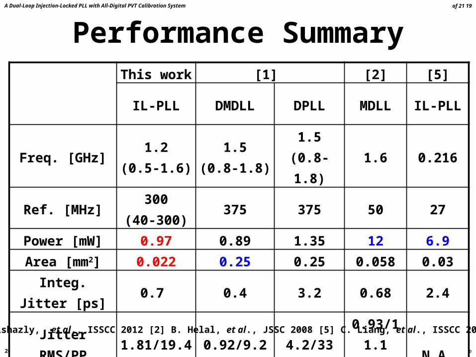
Performance Summary
This work [1] [2] [5]
IL-PLL DMDLL DPLL MDLL IL-PLL
Freq. [GHz] 1.2(0.5-1.6)
1.5(0.8-1.8)
1.5(0.8-1.8) 1.6 0.216
Ref. [MHz] 300(40-300) 375 375 50 27
Power [mW] 0.97 0.89 1.35 12 6.9Area [mm2] 0.022 0.25 0.25 0.058 0.03
Integ. Jitter [ps] 0.7 0.4 3.2 0.68 2.4Jitter RMS/PP
[ps]1.81/19.410M hits
0.92/9.25M hits
4.2/335M hits
0.93/11.130M hits N.A.
FOM [dB] -243 -248.46 -228.59 -233.76 -225CMOS Tech. 65nm 130nm 130nm 130nm 55nm
[1] A. Elshazly, et al., ISSCC 2012 [2] B. Helal, et al., JSSC 2008 [5] C. Liang, et al., ISSCC 2011

©2013 ©2013 電子情報通信学会 総合大会
A Dual-Loop Injection-Locked PLL with All-Digital PVT Calibration System 20 of 21
Conclusion• Dual-loop IL-PLL is suited for SoC
clocking• Low jitter
• Low power consumption
• Small chip area
• Scalability with process
• Insensitivity over PVT
Injectionlocking
All-Digital FLLDual-loop

©2013 ©2013 電子情報通信学会 総合大会
A Dual-Loop Injection-Locked PLL with All-Digital PVT Calibration System 21 of 21
AcknowledgementThis work was partially supported by SCOPE, STARC, NEDO, MIC, MEXT, Canon Foundation, Huawei, and VDEC in collaboration with Cadence Design Systems, Inc., and Agilent Technologies Japan, Ltd.

©2013 ©2013 電子情報通信学会 総合大会
A Dual-Loop Injection-Locked PLL with All-Digital PVT Calibration System 22 of 21

©2013 ©2013 電子情報通信学会 総合大会
A Dual-Loop Injection-Locked PLL with All-Digital PVT Calibration System 23 of 21
Intermit.Calib. at Phase III (1/2)
1 2 1 2 1 2
10us 990us
Step 1: Enable calibration & Replica VCOStep 2: Disable calibration & Replica VCO

©2013 ©2013 電子情報通信学会 総合大会
A Dual-Loop Injection-Locked PLL with All-Digital PVT Calibration System 24 of 21
Intermit. Calib. at Phase III (2/2)Step 1: Enable calibration & Replica VCOStep 2: Disable calibration & Replica VCO
W/O Intermittent 1.6mW
W/ Intermittent 1mW
1 2 1 2 1 2
10us 990us

©2013 ©2013 電子情報通信学会 総合大会
A Dual-Loop Injection-Locked PLL with All-Digital PVT Calibration System 25 of 21
Behavior of Non-ideal InjectionWhen f0 ≠ N· fref

©2013 ©2013 電子情報通信学会 総合大会
A Dual-Loop Injection-Locked PLL with All-Digital PVT Calibration System 26 of 21
Spur LevelLocked state: flocked=N · fref
Free-running: ffree-running=(1+a) · flocked
Spur power = -20log10((ffree-running- flocked)/(2 ·fref))= -20log10(a ·N/2)
e.g. N=20, a=0.001 -60dBc spur[R.B. Staszewski, et al., All-Digital Frequency Synthesizer in Deep-Submicron CMOS, Wiley, 2006]

©2013 ©2013 電子情報通信学会 総合大会
A Dual-Loop Injection-Locked PLL with All-Digital PVT Calibration System 27 of 21
FOM over Area
[1] A. Elshazly, et al., ISSCC 2012 [2] B. Helal, et al., JSSC 2008 [3] J. Lee, et al., JSSC 2009[4] G. Xiang, et al., ISSCC 2009 [5] C. Liang, et al., ISSCC 2011
VLSI 2010SS-PLL
ISSCC 2009SS-PLL[4]
ISSCC 2011MDLL
ISSCC 2011SS-IL-PLL[5]
ISSCC 2002IL-PLL
JSSC 2008MDLL[2]
ISSCC 2012IL-AD-PLL
ISSCC 2012DPLL[1]
ISSCC 2012DMDLL[1] ISSCC 2009
IL-PLL[3]
JSSC 2009IL-PLL
JSSC 2009IL-PLL+DDLL
This WorkIL-PLL
Area [mm2]
FOM
[dB
]
-220
-230
-240
-250
0.01 0.1 1
FOM=, where is the integrating jitter

©2013 ©2013 電子情報通信学会 総合大会
A Dual-Loop Injection-Locked PLL with All-Digital PVT Calibration System 28 of 21
PVT Tracking Capability

©2013 ©2013 電子情報通信学会 総合大会
A Dual-Loop Injection-Locked PLL with All-Digital PVT Calibration System 29 of 21
IL-PLL with Dual VCOs
Frequency offset between main & replica oscillator

©2013 ©2013 電子情報通信学会 総合大会
A Dual-Loop Injection-Locked PLL with All-Digital PVT Calibration System 30 of 21
[D. Park, et al., ISSCC 2012]
Injection Timing (Conventional)

©2013 ©2013 電子情報通信学会 総合大会
A Dual-Loop Injection-Locked PLL with All-Digital PVT Calibration System 31 of 21
Injection Timing (Proposed)
• Injection timing calibration is obliterated

©2013 ©2013 電子情報通信学会 総合大会
A Dual-Loop Injection-Locked PLL with All-Digital PVT Calibration System 32 of 21
Proposed Concept• Dual-loop Topology
– PVT tracking capability– Compensate for main & replica VCO
frequency offset– No calibration for injection timing required
• Reduce area & power overhead• All-digital Frequency-locked Loop
– Compact chip area– Low power consumption– Scalable with process advancement
Related Documents


![Phase locked loops - Universitetet i oslo€¦ · Phase locked loop (PLL) The PLL is a closed loop feedback system that drives Z }v }oÀ}o P }( Z s KU^o} l]vP_] Z to a reference phase,](https://static.cupdf.com/doc/110x72/5ea8b236c60b51394e19c9fe/phase-locked-loops-universitetet-i-oslo-phase-locked-loop-pll-the-pll-is-a-closed.jpg)
