A Detailed Power Model for Field Programmable Gate Arrays KARA K.W. POON STEVEN J.E. WILTON and ANDY YAN University of British Columbia ________________________________________________________________________ Power has become a critical issue for FPGA vendors. Understanding the power dissipation within FPGAs is the first step to develop power-efficient architectures and CAD tools for FPGAs. This paper describes a detailed and flexible power model which has been integrated in the widely-used Versatile Place and Route (VPR) CAD tool. This power model estimates the dynamic, short-circuit, and leakage power consumed by FPGAs. It is the first flexible power model developed to evaluate architectural tradeoffs and the efficiency of power-aware CAD tools for a variety of FPGA architectures, and is freely available for non-commercial use. The model is flexible, in that it can estimate the power for a wide variety of FPGA architectures, and it is fast, in that it does not require extensive simulation, meaning it can be used to explore a large architectural space. We show how the model can be used to investigate the impact of various architectural parameters on the energy consumed by the FPGA, focusing on the segment length, switch block topology, lookup-table size, and cluster size. Categories and Subject Descriptors: B.J.2 [Integrated Circuits]: Design Aids - Power Estimation General Terms: Design, Experimentation, Algorithms Additional Key Words and Phrases: Power estimation model, architecture, power consumption, sensitivity analysis ________________________________________________________________________ This research was supported by Altera, Micronet, and the Natural Sciences and Engineering Research Council of Canada. Preliminary versions of parts of this article appeared in the Proceedings of Conference on Field- Programmable Logic and Applications, 2002 and the Proceedings of the IEEE International Conference on Field-Programmable Technology, 2002. Authors' addresses: Kara K. W. Poon, Steven J. E. Wilton, and Andy Yan, Department of Electrical and Computer Engineering, The University of British Columbia, 2356 Main Mall, Vancouver, BC, Canada, V6T 1Z4; emails: [email protected], [email protected], [email protected]. Permission to make digital/hard copy of part of this work for personal or classroom use is granted without fee provided that the copies are not made or distributed for profit or commercial advantage, the copyright notice, the title of the publication, and its date of appear, and notice is given that copying is by permission of the ACM, Inc. To copy otherwise, to republish, to post on servers, or to redistribute to lists, requires prior specific permission and/or a fee.

Welcome message from author
This document is posted to help you gain knowledge. Please leave a comment to let me know what you think about it! Share it to your friends and learn new things together.
Transcript
A Detailed Power Model for Field Programmable Gate Arrays KARA K.W. POON STEVEN J.E. WILTON and ANDY YAN University of British Columbia ________________________________________________________________________ Power has become a critical issue for FPGA vendors. Understanding the power dissipation within FPGAs is the first step to develop power-efficient architectures and CAD tools for FPGAs. This paper describes a detailed and flexible power model which has been integrated in the widely-used Versatile Place and Route (VPR) CAD tool. This power model estimates the dynamic, short-circuit, and leakage power consumed by FPGAs. It is the first flexible power model developed to evaluate architectural tradeoffs and the efficiency of power-aware CAD tools for a variety of FPGA architectures, and is freely available for non-commercial use. The model is flexible, in that it can estimate the power for a wide variety of FPGA architectures, and it is fast, in that it does not require extensive simulation, meaning it can be used to explore a large architectural space. We show how the model can be used to investigate the impact of various architectural parameters on the energy consumed by the FPGA, focusing on the segment length, switch block topology, lookup-table size, and cluster size. Categories and Subject Descriptors: B.J.2 [Integrated Circuits]: Design Aids - Power Estimation General Terms: Design, Experimentation, Algorithms Additional Key Words and Phrases: Power estimation model, architecture, power consumption, sensitivity analysis ________________________________________________________________________ This research was supported by Altera, Micronet, and the Natural Sciences and Engineering Research Council of Canada. Preliminary versions of parts of this article appeared in the Proceedings of Conference on Field-Programmable Logic and Applications, 2002 and the Proceedings of the IEEE International Conference on Field-Programmable Technology, 2002. Authors' addresses: Kara K. W. Poon, Steven J. E. Wilton, and Andy Yan, Department of Electrical and Computer Engineering, The University of British Columbia, 2356 Main Mall, Vancouver, BC, Canada, V6T 1Z4; emails: [email protected], [email protected], [email protected]. Permission to make digital/hard copy of part of this work for personal or classroom use is granted without fee provided that the copies are not made or distributed for profit or commercial advantage, the copyright notice, the title of the publication, and its date of appear, and notice is given that copying is by permission of the ACM, Inc. To copy otherwise, to republish, to post on servers, or to redistribute to lists, requires prior specific permission and/or a fee.

1 INTRODUCTION
Power dissipation is becoming a major concern for semiconductor vendors and
customers. Power is especially a concern in Field-Programmable Gate Arrays (FPGAs).
The post-fabrication flexibility in these devices is provided using a large number of pre-
fabricated routing tracks and programmable switches. These tracks can be long, and can
consume a significant amount of energy every time they switch. In addition, the
programmable switches add capacitance to each track; this further increases the power
dissipation of FPGAs. Finally, the generic logic structures that are at the heart of every
FPGA consume more power than the dedicated circuitry that would be found on an
ASIC. For all these reasons, FPGA vendors have indicated that power is one of the
primary concerns of their customers.
There has been a modest amount of work developing low-power FPGA architectures
and FPGA CAD algorithms that optimize for low power [George 1999; Hwang 1998;
Kumar 2002; Lesea 2001; Rabaey 1996; Tuan 2001]. Each of these previous studies,
however, has presented “point solutions” for specific FPGA architectures or specific
FPGA CAD programs. In addition, these works tend to use fairly crude models to
estimate the power savings, and often don’t take into account many important design
details that may negate any advantages claimed by the proposed techniques.
Our long-term goal is to understand and investigate the effects of various architectural
and CAD tool optimizations on the power and energy consumed by FPGAs. As a first
step in this effort, we have developed a detailed power model for FPGAs based on the
Versatile Place and Route (VPR) CAD tool. This power model is flexible, in that it can
be used to estimate power in a wide variety of FPGA architectures. It is fast, in that
estimates can be obtained without the time-consuming computation of programs such as
SPICE, or the reliance on simulations, as in [Li 2003]. Also, the model gives good
fidelity; although there may be significant absolute errors in the power estimation, the
power model is capable of evaluating architectural tradeoffs and the efficiency of power-
aware CAD tools based on the relative comparisons among alternative architectures or
algorithms.
In addition to providing comparisons between architectural alternatives or CAD
algorithms, the power model has also been used as an integral part of a power-aware
CAD flow, in which energy dissipation is optimized at every stage from logic synthesis
to physical design [Lamoureux 2003]. We have used this CAD flow in our experiments
to investigate the influence of architectural changes on energy consumption.

This paper is organized as follows. Section 2 introduces the framework of the flexible
power model and how it is incorporated in VPR CAD tool. Section 3 describes the power
model. Section 4 presents an analysis of how architectural changes impact energy
consumption and provides a sensitivity analysis focusing on the primary input density
assumption and the routing algorithm. Finally, conclusions are given in Section 6. The
model is available freely for non-commercial use; the appendix describes how to obtain
the model.
2 VPR FRAMEWORK
The VPR CAD tool is a widely used placement and routing tool available for FPGA
architectural studies [Betz 1999]. As shown in Figure 1, the original VPR has two
components: a place and route tool, and a detailed area and delay model. The place and
route tool maps a circuit to the FPGA. The area and delay models estimate the area and
critical path delay based on results from the place and route tool. The two components
interact with each other to determine the best placement and routing for a user circuit. A
description of the underlying FPGA architecture is provided to the tool in the form of an
architecture file, which contains information such as segment length, connection
topologies, logic block size and composition, and process parameters. The architecture
file is an important feature in VPR – it allows any architecture to be specified, and hence
makes the CAD tool highly flexible.
User
Circuit
ArchitectureDescription
Area/Speed Estimates
Place andRoute Tool
DetailedArea/Delay
Model
Fig. 1: Original VPR framework
Figure 2 shows the modified VPR framework with an activity estimator and a power
model for activity generation and detailed power estimation, respectively. In the baseline
CAD flow, the activity estimator and the power model are not used to guide the
placement and routing. In the power-aware CAD flow, it is possible to use the power
estimates to guide the placement and routing process in order to improve the

effectiveness of the power optimization techniques. The details of the activity generation
and power estimation modules will be described in Section 3.
User
Circuit
ArchitectureDescription
Area/Speed/Power Estimates
VPR(Place and
Route)
DetailedArea/Delay/
PowerModel
ActivityEstimator
Fig. 2: Modified VPR Framework
3 POWER MODEL
Our power model is aimed at island-style FPGA architectures, which have logic
blocks, switch blocks, connection blocks, and routing, as shown in Figure 3, with an H-
tree clock network, as shown in Figure 4. The model has two modules: an activity
generation module, and a power estimation module. The first module employs the
transition density model to determine the switching activities inside the circuit. The
second module estimates the power consumption at the transistor level. The model was
calibrated using HSPICE with the technology parameters from TSMC for a 1.8 volt,
0.18�m CMOS technology. However, the model is general enough to apply to any
technology.
ClockSegment
Clock Buffers
SwitchBlock
ProgrammableRouting Switch
LogicBlock
ConnectionBlock
ProgrammableConnection
Switch
Fig. 3: Island-style FPGA (from [Betz 1999])
Fig. 4: H-tree clock network

3.1 Activity Generation Probabilistic techniques are preferred for our activity generation step because of their
efficiency in computation. Among all the available probabilistic techniques, the
Transition Density Model is the most accurate [Yeap 1998]. Therefore, the Transition
Density Model is employed in this power model. The Transition Density model is based
on two parameters for each signal: the transition density and the static probability. The
transition density of a signal represents the average number of transitions of that signal
per unit time, and the static probability is the probability of the signal being high at any
given time. The transition density and static probability values of all the signals are
calculated iteratively from the primary inputs to the primary outputs. The propagation of
transition density through each lookup-table (LUT) can be determined by Equation (1)
[Najm 1994]. As all LUT inputs are assumed to be uncorrelated to each other, each input
contributes a static probability, P(�f(x)/�xi), and a transition density, D(xi), to the total
density, D(y), at the output.
)()()(
i
inputsall ixD
xxfPyD �� ���
����
�
(1)
Even though the original Transition Density Model applies only to combinational
circuits, it can be extended to sequential circuits. For D flip-flops, the output probability
can be set to be the same as the input probability. The transition density of the output,
D(y), of the flip-flop can be modeled as its transition probability, Pt(y), written as [Najm
1995].
))(1()(2)()( xPxPyPyD t �����
(2)
where P(x) represents the probability that signal x is high. For each sequential feedback
loop, a mutual probability is determined for the output of each D-flip-flop through
iterations. Even though this is an approximate method for calculating the transition
probabilities of the signals in the feedback loops, a previous study shows that the average
error obtained by using this method for three iterations is less than 5% [Tsui 1994].
Due to unequal gate and wire delays in a logic network, the voltage on internal signals
may switch more than once during a single clock cycle, before stabilizing. These small
pulses are often called glitches, and are an important component of the total overall
power. However, the original Transition Density model does not consider the fact that
pulses shorter than the propagation delay of a gate are filtered out because the gate cannot

respond fast enough [Najm 1994]. To simulate the filtration effect of circuit inertial
delays, a “low pass filter” is modeled at the output of each gate (each LUT in an FPGA)
as shown in Figure 5. A transition at y is transmitted across the filter only when the input
remains stable over a certain period of time. A probability distribution function, with the
pulse width as a parameter, is used to determine whether an input pulse is propagated to
the output [Najm 1994].
Logic Module
Look-Up-Table(LUT) Low-pass Filter
x0
x1
xn
z
y
Fig. 5: Model of the low-pass filter for each LUT (from [Najm 1994])
As shown in Figure 6, activity estimation is carried out in three steps: LUT
organization, static probability calculation and transition density calculation. First, LUTs
are ordered from the primary inputs to the primary outputs. For sequential circuits, the
outputs of the flip-flops are initially assumed to be primary inputs. Then, the calculation
of the static probability is carried out for each LUT output signal. In sequential circuits,
several iterations may be required. Finally, the transition density calculation is performed.
As part of the transition density calculation, the CAD tool determines whether glitches
exist at the output of each LUT; the low-pass filter is applied at the output of the LUT to
eliminate unrealistic activity values.

Organize LUTs from primary inputs to primary outputs;/* Static Probability Calculation */do { For (each LUT in the organized order) {
Calculate static probability; Update the static probability in the database;
}} until (static probability difference < error tolerance)
/* Transition Density Calculation */for (each LUT in the organized order){
Calculate transition density;If glitches exist at the output{
apply the filter (static probability, transition density);}Update transition density and static probability in the database;
}
Fig. 6: Pseudo-code of the transition density algorithm
3.2 Dynamic Power estimation
After the switching activities have been determined, the next step is to analyze the
power dissipation at the transistor level for each component inside the FPGA. The
average power consumption in digital circuits consists of three main components:
dynamic, short-circuit and leakage power [Kang 1999]. The estimation methodology for
these three components will be described in this and the following two sections. The
model for each component has been evaluated using HSPICE.
Dynamic power is the dominant component of the total power. It is dissipated every
time a signal changes due to the charging and discharging of load and parasitic
capacitances. Therefore, dynamic power is closely related to the transition density of all
nodes inside the circuit. The total dynamic power dissipation can be written as:
clkswingsupply
y )( 5.0Power Dynamic fyDVVC
nodesall
������ � (3)
The expression )(5.0 swingsupplyy yDVVC ���� determines the energy per clock cycle, where
Vswing is the swing voltage of each node, Vsupply is the supply voltage, D(y) is the
transition density at node y, and Cy is the capacitance of node y that is charged and
discharged during each transition. The dynamic power is then equal to the energy per
clock cycle multiplied by the clock frequency, fclk, which is bounded by the critical path
delay of the circuit.

3.2.1 Routing Resource Dynamic Power
To estimate dynamic power, we separate the resources in an FPGA into three
categories: routing resources, logic blocks, and the clock network. We estimate the
power dissipated by resources in each category separately. This subsection focuses on
the power dissipated in the routing fabric; the next two subsections focus on the logic
blocks and the clock network.
A large part of the dynamic power is due to switching tracks within the routing fabric
of the FPGA. As described in Section 3.1, the power dissipated in the fabric can be
calculated using the transition density and capacitance of each track. Since we wish our
power model to be flexible enough to model the power in any FPGA that can be
described within VPR, and since the capacitances of the routing tracks vary greatly with
the track length and the number of attached buffers, a single value for track capacitance
will not suffice. Instead, we extract capacitance information from the routing resource
graph within VPR for each metal track separately. Figure 7 shows an example metal
track that spans four logic blocks and is attached to a number of programmable switches.
In general, the capacitance of a track depends on the number of logic blocks spanned by
the segment, the size of each logic block (since a larger logic block implies a longer
metal track), the number of pins on each logic block, the switch block and connection
block connectivities, and information about the target technology. The sizes of each of
the buffers were estimated in [Betz 1999] to optimize the speed of the FPGA. Using this
information, the overall capacitance of each track is estimated by adding the metal
capacitance of the track itself and the parasitic capacitances of all switches attached to the
track. More details on the routing resource graph and the capacitance calculation can be
found in [Betz 1999].
5x 5x 5x 5x 5x 5x 5x 5x
5x5x5x
5x5x5x
5x
Fig. 7: Example FPGA Routing Segment

Fig. 8: Algorithm for calculating dynamic power of the routing fabric
After calculating the capacitance information for each track, the overall dynamic
power of the routing fabric is calculated. For each net in the design, the capacitance of
all tracks that are used to route the net are summed, and the activity of the net is then
used, along with this capacitance, to calculate the power dissipated by that net. This is
summarized in Figure 8.
To verify the model, an HSPICE model was created. Figure 9 shows the power
predicted by the model along with the power predicted by HSPICE, for a range of
segment lengths. The wires were switched at 20MHz to ensure that the wires had fully
charged or discharged during each cycle. As the graph shows, the model results match the
HSPICE results very closely, with an average error of 4.8%.
Fig. 9: Comparison of our model and HSPICE for one routing segment

LUT DFF
SRAM
Set/Reset logic
SRAM1x 4x
1x 4x
1x 4x
1x 4x
1x 4x1x
SRAM
1x
output1input 1
input n
clock
Set/Reset
Fig. 10: Schematic of a logic block (from [Betz 1999])
3.2.2 Logic Block Dynamic Power
Like the power model for the routing fabric, the power model for the logic block must
be flexible. It must accommodate any lookup-table size, any number of lookup-tables in
each cluster, and any number of inputs to each cluster. The model assumes the
architecture in Figure 10, and consists of four components: the power dissipated in the
lookup-tables, the power dissipated in the input multiplexers, the power dissipated in the
flip-flops, and the power dissipated in the other nodes and wires within the logic block.
a) Power Dissipated in the Lookup-Tables
Lookup-tables in FPGA’s are commonly implemented as multiplexer trees. To
estimate the power dissipated in a multiplexer tree, we represent the tree as a set of two-
input multiplexers as shown in Figure 11. We then use the transition density model (as
before) to estimate the activity of each node within the lookup-table. The capacitance of
each node within the lookup-table is estimated by noting that each node is associated with
three source/drain capacitances and one gate capacitance (the gate capacitance is due to
the Miller effect spread over two transistors as described in [Kang99]).

output
SRAM
SRAM
SRAM
SRAM
input 0 input 1
output
SRAM
SRAM
SRAM
SRAM
input 0 input 1
Fig. 11: Modeling of a 2-input look-up-table using 2-input multiplexers
To verify the model, an HSPICE simulation was used. The power predicted by the
HSPICE simulation depends heavily on the relative switching times of the inputs. Since
our model does not take this into account, we performed several thousand HSPICE
simulations, each with different relative input switching times. For each combination of
input arrival times, we measured the power predicted by HSPICE. Figure 12 (a) shows
the maximum power obtained from the HSPICE simulations (over all signal arrival time
combinations), the minimum power obtained from the HSPICE simulations, and the
average power obtained from the HSPICE simulations, all as a function of the transition
density of each input. The measurements obtained from our model are plotted on the
same graph. As the graph shows, our estimate lies within the maximum and minimum
HSPICE predictions. The graph also illustrates that the model power is closer to the
maximum HSPICE prediction than the minimum prediction; this is expected because the
transition signal density model assumes all inputs to the multiplexers are switching at
different times, which is the worst-case scenario. Figure 12(b) shows the same results as
a function of the lookup-table size; again, the same conclusions hold. Note that, in both
sets of results, the fidelity (relative difference between power estimates) between the
model predictions and HSPICE results is very good. The average difference between the
maximum HSPICE prediction and the modeled values is 14.5%.
Input Transition Density
Pow
er (i
n uW
)
0
5
10
15
20
25
30
35
40
45
0.1 0.2 0.3 0.4 0.5 0.6 0.7 0.8 0.9 1.0
Maximum HSPICE Power
Minimum HSPICE Power
Average HSPICE Power
Model Power
LUT Size
Pow
er (i
n uW
)
0
10
20
30
40
50
60
2 3 4 5 6 7
Maximum HSPICE PowerMinimum HSPICE PowerAverage HSPICE PowerModel Power
a) As a function of transition density b) As a function of lookup-table size Fig. 12: Comparison of model and HSPICE results for lookup-tables
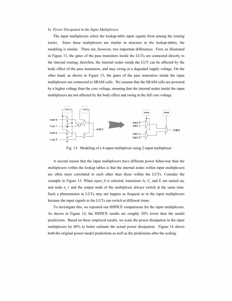
b) Power Dissipated in the Input Multiplexers
The input multiplexers select the lookup-table input signals from among the routing
tracks. Since these multiplexers are similar in structure to the lookup-tables, the
modeling is similar. There are, however, two important differences. First, as illustrated
in Figure 11, the gates of the pass transistors inside the LUTs are connected directly to
the internal routing; therefore, the internal nodes inside the LUT can be affected by the
body effect of the pass transistors, and may swing at a degraded supply voltage. On the
other hand, as shown in Figure 13, the gates of the pass transistors inside the input
multiplexers are connected to SRAM cells. We assume that the SRAM cells are powered
by a higher voltage than the core voltage, meaning that the internal nodes inside the input
multiplexers are not affected by the body effect and swing at the full core voltage.
Fig. 13: Modeling of a 4-input multiplexer using 2-input multiplexer
A second reason that the input multiplexers have different power behaviour than the
multiplexers within the lookup tables is that the internal nodes within input multiplexers
are often more correlated to each other than those within the LUTs. Consider the
example in Figure 13. When input_0 is selected, transistors A, C, and E are turned on,
and node n_1 and the output node of the multiplexer always switch at the same time.
Such a phenomenon in LUTs may not happen as frequent as in the input multiplexers
because the input signals to the LUTs can switch at different times.
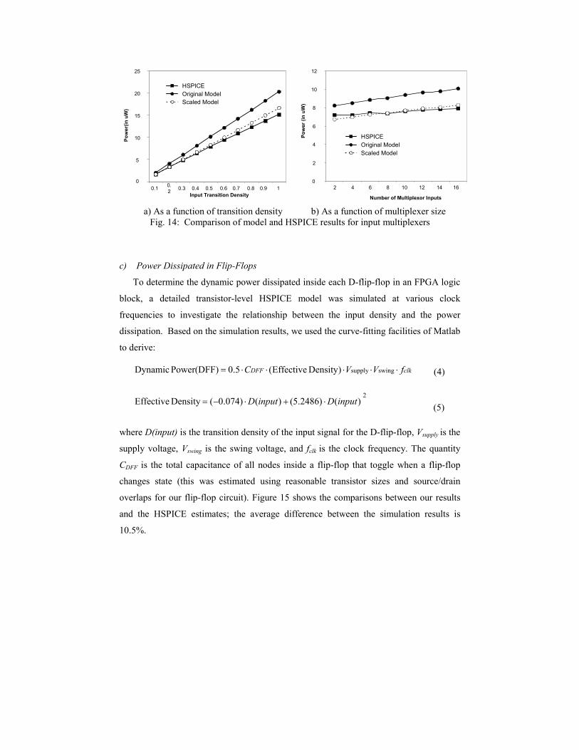
To investigate this, we repeated our HSPICE comparisons for the input multiplexers.
As shown in Figure 14, the HSPICE results are roughly 20% lower than the model
predictions. Based on these empirical results, we scale the power dissipation in the input
multiplexers by 80% to better estimate the actual power dissipation. Figure 14 shows
both the original power model predictions as well as the predictions after the scaling.
0
5
10
15
20
25
0.1 0.2 0.3 0.4 0.5 0.6 0.7 0.8 0.9 1
Input Transition Density
Pow
er(in
uW
)
0
2
4
6
8
10
12
2 4 6 8 10 12 14 16
Number of Multiplexor Inputs
Pow
er (i
n uW
)Scaled ModelOriginal ModelHSPICE
Scaled ModelOriginal ModelHSPICE
a) As a function of transition density b) As a function of multiplexer size Fig. 14: Comparison of model and HSPICE results for input multiplexers
c) Power Dissipated in Flip-Flops
To determine the dynamic power dissipated inside each D-flip-flop in an FPGA logic
block, a detailed transistor-level HSPICE model was simulated at various clock
frequencies to investigate the relationship between the input density and the power
dissipation. Based on the simulation results, we used the curve-fitting facilities of Matlab
to derive:
clkDFF fVVC ������ swingsupply)Density Effective(5.0Power(DFF) Dynamic
(4)
2)()2486.5()()074.0(Density Effective inputDinputD �����
(5)
where D(input) is the transition density of the input signal for the D-flip-flop, Vsupply is the
supply voltage, Vswing is the swing voltage, and fclk is the clock frequency. The quantity
CDFF is the total capacitance of all nodes inside a flip-flop that toggle when a flip-flop
changes state (this was estimated using reasonable transistor sizes and source/drain
overlaps for our flip-flop circuit). Figure 15 shows the comparisons between our results
and the HSPICE estimates; the average difference between the simulation results is
10.5%.
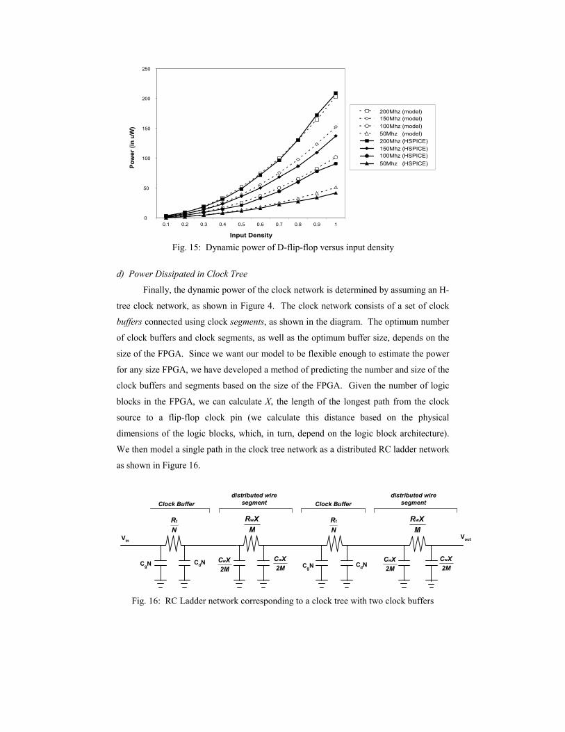
Input Density
Pow
er (i
n uW
)
0
50
100
150
200
250
0.1 0.2 0.3 0.4 0.5 0.6 0.7 0.8 0.9 1
200Mhz (model)150Mhz (model)100Mhz (model)50Mhz (model)200Mhz (HSPICE)150Mhz (HSPICE)100Mhz (HSPICE)50Mhz (HSPICE)
Fig. 15: Dynamic power of D-flip-flop versus input density
d) Power Dissipated in Clock Tree
Finally, the dynamic power of the clock network is determined by assuming an H-
tree clock network, as shown in Figure 4. The clock network consists of a set of clock
buffers connected using clock segments, as shown in the diagram. The optimum number
of clock buffers and clock segments, as well as the optimum buffer size, depends on the
size of the FPGA. Since we want our model to be flexible enough to estimate the power
for any size FPGA, we have developed a method of predicting the number and size of the
clock buffers and segments based on the size of the FPGA. Given the number of logic
blocks in the FPGA, we can calculate X, the length of the longest path from the clock
source to a flip-flop clock pin (we calculate this distance based on the physical
dimensions of the logic blocks, which, in turn, depend on the logic block architecture).
We then model a single path in the clock tree network as a distributed RC ladder network
as shown in Figure 16.
CdNCgN
VinVout
Clock Bufferdistributed wire
segment Clock Bufferdistributed wire
segment
2MXCw
NRt
MXRw
2MXCw
CgN CdN
NRt
2MXCw
2MXCw
MXRw
Fig. 16: RC Ladder network corresponding to a clock tree with two clock buffers

In general, there are M stages (corresponding to M clock buffers), and each clock
buffer is of size N. In the example of Figure 16, M=2. By solving the RC equation
corresponding to the ladder network, and by differentiating with respect to N and M, we
can estimate the number of clock buffers as
)CC(*R*2
XCRM
gdt
2ww
�
� (6)
and the relative drive strength of each buffer as:
gw
wt
CRCRN � (7)
where Rw and Cw are the wire resistance and capacitance per unit length, Rt represents the
resistance of the clock buffer, and Cg and Cd represent gate and drain capacitance of the
clock buffer. Using these values of M and N, the power dissipated in the clock network
can be calculated as before.
3.3 Short-Circuit Power
Short-circuit power is dissipated through a direct current path between the power
supply and ground during each transition. Short-circuit power is a function of the rise and
fall time and the load capacitance [Eckerbert 2001; Wang 1999]. We model the short-
circuit power as 10% of the dynamic power calculated in Section 3.2. This percentage
was obtained using HSPICE simulations and parameters from FPGA datasheets [Altera
2001] [Xilinx 2001].
3.4 Leakage Power
Leakage power dissipation comes from two sources: reverse-bias leakage power and
sub-threshold leakage power. As the majority of leakage power is from sub-threshold
current [Leshavarzi 1997]; the reverse bias leakage current is assumed to be negligible. A
first-order estimation model is applied to estimate the sub-threshold current [Kang 1999]:
���
�
���
� ��
nkTqVV
II ongsondrain
)(exp)( inversionweak
(8)

where Von is the boundary between the weak and strong inversion regions. The following
equation is used to calculate Von :
q
nkTVV ton �� (9)
���
����
��
��
����
��
ox
d
ox
FS
CC
CqNn 1 (10)
where Ion is the drain current at the boundary when Vgs is equal to Von. The velocity
saturation model [Toh 1988] is employed to calculate Ion:
effctgs
tgsoxsaton LEVV
VVCvWI
��
�
�
)()( 2
(11)
where W is the device width, vsat is electron velocity, Ec is the piecewise carrier drift
velocity, Leff is the effective source-drain channel length, Vgs is the gate-source voltage, Vt
is the threshold voltage, and Cd is the capacitance associated with the depletion region.
The constants k and q are Boltzman’s constant and the elementary charge, respectively.
T is the temperature in Kelvins.
The quantity NFS is the number of fast surface states. It is a current fitting parameter
that determines the slope of the sub-threshold current-voltage characteristic [Kang 1999].
Each temperature has a specific NFS value. To determine the NFS values of NMOS and
PMOS transistors, HSPICE simulations have been run for both types of transistors, with
different transistor sizes and over the temperature range from -40 to 100 �C. To be
conservative, the Vgs value is assumed to be half of the threshold—0.2V. The average
error between the estimated values and the simulated results is 13.4%. The leakage
power is calculated by multiplying the sub-threshold current with the supply voltage:
tagesupply_voldrain )(IPower Leakage inversionweak V��
(12)
All the logic blocks and routing switches, including the unused logic blocks and unused
routing switches, are considered in the leakage power calculation. The leakage current of
each SRAM cell can be defined by the users in the architecture input file in order to
include the SRAM leakage in the power estimation.

Logic Optimization (SIS)
Technology Mapping[flowmap for baseline; emap for power-aware]
Placement (VPR)[T-Vplace for basline; P-T-Vplack for power-aware]
Routing (VPR)[VPR for basline; P-VPR for power-aware]
Min #Tracks?
Adjust channelwidth (W)
Route with W=1.2 Wmin[Timing-Driven Router for baseline;
Activity/Timing-Driver Router for power-aware]
Power Estimation (VPR)
ActivityGeneration
(ACE)
Packing[T-Vpack for basline; P-T-Vpack for power-aware]
Circuits
ArchitectureParameter
File
No
Yes
Power-aware flow only
Power-aware flow only
Power-aware flow only
Power-aware flow only
Power-aware flow only
Fig. 17: Architectural evaluation flow [Betz 1999]
4 ARCHITECTURE EXPERIMENTS AND SENSITIVITY ANALYSIS
4.1 Methodology To investigate the impact of architectural parameters on the power consumption of an
FPGA, we conducted experiments using both the baseline FPGA CAD flow [Betz 1999]
and a power-aware FPGA CAD flow [Lamoureux 2003]. We followed the architecture
evaluation flow proposed in [Betz 1999]. This architecture flow is outlined in Figure 17.
Each benchmark circuit was optimized by SIS [Sentovich 1992]. In the baseline flow,
each circuit was technology-mapped using FlowMap [Cong 1994]. Each circuit was then
packed into logic clusters using TVPack [Betz 2000] and placed and routed using VPR
[Betz 1999]. The activity estimator was applied to the mapped circuit to estimate the
transition densities for all the nodes. In the power-aware flow, the activity of each node is
used to guide the technology-mapping (Emap), clustering (P-T-Vpack), placement, and
routing (PVPR) steps. In all cases, the smallest square FPGA with sufficient logic blocks
and pads was assumed. VPR and PVPR are employed to determine the minimum number
of tracks (Wmin) required for the circuit. Then, we perform a final “low-stress” routing of
each circuit with the number of tracks per channel set to 20% more than Wmin. Fixed

channel widths for each given benchmark circuit are used to ensure that the architectures
used in both CAD flows are the same in order to produce unbiased experimental results.
Detailed power estimation is performed at the end using the activity, capacitance and
timing information obtained throughout logic synthesis, placement, and routing. The 20
largest Microelectronics Centre of North Carolina (MCNC) benchmark circuits are used
for these experiments. SRAM cells are assumed to use high threshold voltage devices, in
which leakage current is negligible.
Instead of using power for evaluation, we express our results in terms of energy.
Energy is the product of the clock period at which the circuit is run and the power
dissipated by the circuit. Using energy as the metric can avoid favoring architectures and
implementations where the power is reduced simply by slowing down the clock. Of
course, this does not imply that the most energy-efficient architecture is necessarily the
best; an FPGA designer would need to tradeoff delay for energy, depending on the target
market and intended applications.
Our experiments focus on the effects of the four architectural parameters listed in
Table I. We vary these parameters one at a time. The routing architecture consists of
50% pass-transistor switched wires and 50% tri-state buffer switched wires. The fraction
of wires in each channel to a logic block input pin, Fc_input, is 0.6, and the fraction of
wires in each channel to a logic block output, Fc_output, is 0.25 for the architecture with
4-input LUTs and a cluster size of 4. As the cluster and LUT sizes change, the number of
cluster inputs, routing switch sizes, and wire length per unit segment are adjusted
accordingly [Ahmed 2000]. The static probability and the transition density for each
primary input are set to 0.5. In all cases, we assumed a 0.18�m CMOS technology using
a Vdd of 1.8V.
Table I: Parameters under investigation
Parameters Description Segment_length The number of logic blocks spanned by each wire segment Switch_block Switch block topology Cluster_size The number of LUTs per logic block LUT_size The number of inputs per look-up-table

4.2 Segment Length and Switch Block Topology The FPGA routing fabric consists of many prefabricated segments. The length of
these prefabricated segments is one of the key decisions that an FPGA architect must
make. In [Betz 1999], it is shown that a segment that spans four logic blocks is good for
speed and area; in this section, we determine which segment lengths work well for
energy. Intuitively, the longer each routing segment, the more energy it will require to
switch the segment. On the other hand, longer segments result in fewer switches. This
may result in a decrease in energy.
Since the optimum choice for segment length is so tightly coupled with the optimum
choice for the switch block topology, we consider both parameters in the same set of
experiments. Four switch block topologies, Disjoint [Lemieux 1993], Universal [Chang
1996], Wilton [Masud 1999], and Imran [Masud 1999] are considered. The four
topologies are shown in Figures 18 and 19. The disjoint switch block connects each pin
to pins with the same pin number on the three other sides of the switch block. The
Universal switch block focuses on maximizing the number of signals that can be made
through a switch block at the same time. The Wilton switch block is similar to the
Disjoint, except that the diagonal connections from the pins are rotated by one track. A
previous study shows that the Wilton switch block provides good routing flexibility, but
lower area-efficiency when long segments are employed, compared with Disjoint block
[Vaughn 1999]. The fourth topology, the Imran switch block, provides both good
flexibility and area-efficiency by combining aspects of the Disjoint topology and the
Wilton topology [Masud 1999].
0 1 2 3
3
2
1
0
3
2
1
0
0 1 2 3
Top
Bottom
Left Right
0 1 2 3
3
2
1
0
3
2
1
0
0 1 2 3
Top
Bottom
Left Right
0 1 2 3
3
2
1
0
3
2
1
0
0 1 2 3
Top
Bottom
Left Right
a) Disjoint b) Universal c) Wilton
Fig. 18: Disjoint, Universal, and Wilton switch block topologies [Masud 1999]

Disjoint topology fortracks that bypass theswitch block
Wilton topology fortracks that terminateat the switch block
combinedconnections
Fig. 19: Imran switch block [Masud 1999]
Figure 20 shows the impact of segment length and switch block topology on the
routing energy dissipation, averaged over all benchmark circuits. In these experiments,
the number of inputs per lookup table was kept at four, and the number of lookup-tables
per cluster was also fixed at four. The segment length was varied from 1 to 16 (all
segments were assumed to have the same length). The results from both CAD flows
show that circuits dissipate less energy when routed with shorter wires. This conclusion
further confirms the finding from [Shang 2002] that FPGA designs should take advantage
of the locality of wire connections. In addition, the results show that the Imran and
Disjoint switch block topologies are preferable for all segment lengths.
0
1.0
2.0
3.0
4.0
5.0
6.0
1 2 4 8 16Segment Length
Rou
ting
Ener
gy (n
J)
Disjoint (Baseline)
Universal (Baseline)
Imran (Baseline)
Wilton (Baseline)
Disjoint (Power-aware)
Universal (Power-aware)
Imran (Power-aware)
Wilton (Power-aware)
Fig. 20: Routing Energy versus segment length
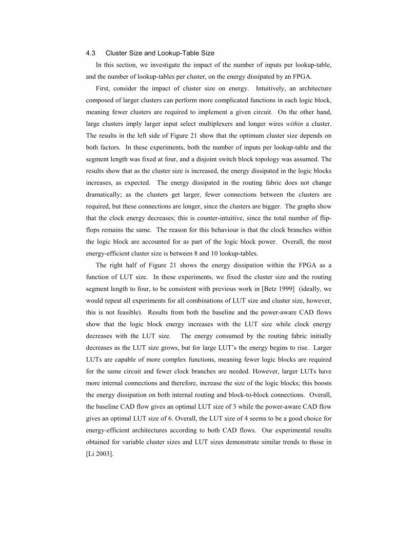
4.3 Cluster Size and Lookup-Table Size
In this section, we investigate the impact of the number of inputs per lookup-table,
and the number of lookup-tables per cluster, on the energy dissipated by an FPGA.
First, consider the impact of cluster size on energy. Intuitively, an architecture
composed of larger clusters can perform more complicated functions in each logic block,
meaning fewer clusters are required to implement a given circuit. On the other hand,
large clusters imply larger input select multiplexers and longer wires within a cluster.
The results in the left side of Figure 21 show that the optimum cluster size depends on
both factors. In these experiments, both the number of inputs per lookup-table and the
segment length was fixed at four, and a disjoint switch block topology was assumed. The
results show that as the cluster size is increased, the energy dissipated in the logic blocks
increases, as expected. The energy dissipated in the routing fabric does not change
dramatically; as the clusters get larger, fewer connections between the clusters are
required, but these connections are longer, since the clusters are bigger. The graphs show
that the clock energy decreases; this is counter-intuitive, since the total number of flip-
flops remains the same. The reason for this behaviour is that the clock branches within
the logic block are accounted for as part of the logic block power. Overall, the most
energy-efficient cluster size is between 8 and 10 lookup-tables.
The right half of Figure 21 shows the energy dissipation within the FPGA as a
function of LUT size. In these experiments, we fixed the cluster size and the routing
segment length to four, to be consistent with previous work in [Betz 1999] (ideally, we
would repeat all experiments for all combinations of LUT size and cluster size, however,
this is not feasible). Results from both the baseline and the power-aware CAD flows
show that the logic block energy increases with the LUT size while clock energy
decreases with the LUT size. The energy consumed by the routing fabric initially
decreases as the LUT size grows, but for large LUT’s the energy begins to rise. Larger
LUTs are capable of more complex functions, meaning fewer logic blocks are required
for the same circuit and fewer clock branches are needed. However, larger LUTs have
more internal connections and therefore, increase the size of the logic blocks; this boosts
the energy dissipation on both internal routing and block-to-block connections. Overall,
the baseline CAD flow gives an optimal LUT size of 3 while the power-aware CAD flow
gives an optimal LUT size of 6. Overall, the LUT size of 4 seems to be a good choice for
energy-efficient architectures according to both CAD flows. Our experimental results
obtained for variable cluster sizes and LUT sizes demonstrate similar trends to those in
[Li 2003].

It is interesting to compare the impact of logic cluster size and logic block size on
energy. Intuitively, we may expect that a change in LUT size will have a more
significant effect on overall power than a change in cluster size, since the area due to the
LUT increases exponentially as the number of inputs to the LUT increase. The graphs
show, however, that both architectural parameters have a similar impact on power. There
is a fundamental difference between increasing the LUT size and increasing the cluster
size. As the LUT size is increased, fewer LUTs are required, meaning there are fewer
flip-flops, less routing, and (importantly) fewer clock connections. These tend to
counter-act the exponential increase in power that would be intuitively expected.
Although the logic block area does go up quadratically, the area of the LUT itself is
much smaller than the area of the input multiplexers and the rest of the cluster circuitry,
meaning that the exponential effect is not seen. On the other hand, increasing the cluster
size essentially re-arranges the LUTs within the fabric. The total logic area is not
reduced, since the same number of LUTs and clock connections are required, regardless
of cluster size.
0
0.5
1.0
1.5
2.0
2.5
3.0
3.5
4.0
2 4 6 8 10 12 14 16 18 20Cluster Size
Ener
gy (n
J)
0
0.5
1.0
1.5
2.0
2.5
3.0
3.5
2 3 4 5 6 7LUT Size
Ener
gy (n
J)
Routing (Baseline)
Logic Block (Baseline)
Clock (Baseline)
Total (Baseline)
Routing (Power-aware)
Logic Block (Power-aware)
Clock (Power-aware)
Total (Power-aware)
Fig. 21: Energy versus cluster size and energy versus look-up-table (LUT) size
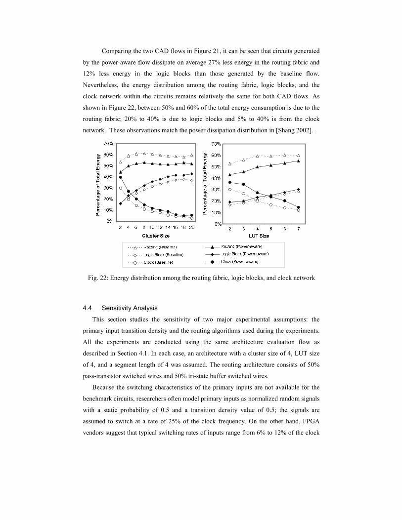
Comparing the two CAD flows in Figure 21, it can be seen that circuits generated
by the power-aware flow dissipate on average 27% less energy in the routing fabric and
12% less energy in the logic blocks than those generated by the baseline flow.
Nevertheless, the energy distribution among the routing fabric, logic blocks, and the
clock network within the circuits remains relatively the same for both CAD flows. As
shown in Figure 22, between 50% and 60% of the total energy consumption is due to the
routing fabric; 20% to 40% is due to logic blocks and 5% to 40% is from the clock
network. These observations match the power dissipation distribution in [Shang 2002].
Fig. 22: Energy distribution among the routing fabric, logic blocks, and clock network
4.4 Sensitivity Analysis
This section studies the sensitivity of two major experimental assumptions: the
primary input transition density and the routing algorithms used during the experiments.
All the experiments are conducted using the same architecture evaluation flow as
described in Section 4.1. In each case, an architecture with a cluster size of 4, LUT size
of 4, and a segment length of 4 was assumed. The routing architecture consists of 50%
pass-transistor switched wires and 50% tri-state buffer switched wires.
Because the switching characteristics of the primary inputs are not available for the
benchmark circuits, researchers often model primary inputs as normalized random signals
with a static probability of 0.5 and a transition density value of 0.5; the signals are
assumed to switch at a rate of 25% of the clock frequency. On the other hand, FPGA
vendors suggest that typical switching rates of inputs range from 6% to 12% of the clock
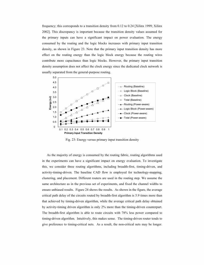
frequency; this corresponds to a transition density from 0.12 to 0.24 [Xilinx 1999; Xilinx
2002]. This discrepancy is important because the transition density values assumed for
the primary inputs can have a significant impact on power evaluation. The energy
consumed by the routing and the logic blocks increases with primary input transition
density, as shown in Figure 23. Note that the primary input transition density has more
effect on the routing energy than the logic block energy because the routing wires
contribute more capacitance than logic blocks. However, the primary input transition
density assumption does not affect the clock energy since the dedicated clock network is
usually separated from the general-purpose routing.
0.1 0.2 0.3 0.4 0.5 0.6 0.7 0.8 0.9 1Primary Input Transition Density
Ener
gy (n
J)
0
0.5
1.0
1.5
2.0
2.5
3.0
3.5
4.0
4.5
5.0
Routing (Baseline)
Logic Block (Baseline)
Clock (Baseline)
Total (Baseline)
Routing (Power-aware)
Logic Block (Power-aware)
Clock (Power-aware)
Total (Power-aware)
Fig. 23: Energy versus primary input transition density
As the majority of energy is consumed by the routing fabric, routing algorithms used
in the experiments can have a significant impact on energy evaluation. To investigate
this, we consider three routing algorithms, including breadth-first, timing-driven, and
activity-timing-driven. The baseline CAD flow is employed for technology-mapping,
clustering, and placement. Different routers are used in the routing step. We assume the
same architecture as in the previous set of experiments, and fixed the channel widths to
ensure unbiased results. Figure 24 shows the results. As shown in the figure, the average
critical path delay of the circuits routed by breadth-first algorithm is 5.9 times more than
that achieved by timing-driven algorithm, while the average critical path delay obtained
by activity-timing driven algorithm is only 2% more than the timing-driven counterpart.
The breadth-first algorithm is able to route circuits with 78% less power compared to
timing-driven algorithm. Intuitively, this makes sense. The timing-driven router tends to
give preference to timing-critical nets. As a result, the non-critical nets may be longer.

The goal of the breadth-first router is to minimize the total capacitance, which, in the
absence of activity information, is the best way to reduce power. The timing-driven
router is less concerned with minimizing the total capacitance, and more concerned with
optimizing the capacitance specifically on the critical nets. The activity-driven algorithm,
on the other hand, can only achieve an average power consumption which is 4% lower
than that obtained by timing-driven algorithm.
In terms of energy, circuits routed using breadth-first algorithm consumed, on
average, 30% more energy than those routed using timing-driven algorithm, and circuits
routed using the timing-driven algorithm dissipate, on average, 5% more energy than
those routed by the activity-timing-driven algorithm. These results are shown in Figure
25.
The purpose of these experiments is not to compare the routers, but instead, to
investigate the sensitivity of the architectural conclusions on the routing assumptions.
From Figure 25, it is clear that if the breadth-first algorithm is used, a different
conclusion regarding segment length would be drawn. This is in-line with observations
in [Yan 2002].
0
20
40
60
80
100
120
140
1 2 4 8 16Segment Length
Rou
ting
Pow
er (m
W)
0
100
200
300
400
500
600
1 2 4 8 16Segment Length
Criti
cal P
ath
Dela
y (n
s)
Breadth-First Timing-Driven Activity-Timing-Driven Fig. 24: The effect of different routing algorithms on critical path delay and power

00.51.01.52.02.53.04.54.04.55.0
1 2 4 8 16Segment Length
Rou
ting
Ener
gy (n
J)
Breadth-FirstTiming-DrivenActivity-Timing-Driven
Fig. 25: Routing energy versus segment length for different routing algorithms
5 CONCLUSIONS
In this paper, we have presented a detailed power model that is flexible enough to
estimate power dissipation on a wide variety of island-style FPGA architectures. The tool
is flexible, in that it can be used to estimate power in a wide variety of FPGA
architectures. It is fast, in that estimates can be obtained without the time-consuming
computation of programs such as SPICE, or the reliance on simulations. Finally, the
model gives good fidelity; although there may be significant absolute errors in the power
estimation, the power model is capable of evaluating architectural tradeoffs and the
efficiency of power-aware CAD tools based on the relative comparisons among
alternative architectures or algorithms.
We have shown how the model can be used to evaluate architectural tradeoffs and
estimate the effectiveness of CAD tools. Both the baseline (timing-driven) and power-
aware FPGA CAD flow is applied for our evaluation. We have found that short segments
are more energy-efficient than long segments, that the Disjoint and Imran switch block
topologies are more energy efficient than the Wilton or Universal topologies, and that a
cluster size of 8-10 and a lookup-table size of 4 is most energy efficient.
Our study confirms that routing fabric contributes to a major portion of the total
energy. FPGA designers should take advantage of short wires. Our investigation also
indicates that energy evaluation can be affected by assumptions regarding the primary
input transition density and the routing algorithm.

6 ACKNOWLEDGMENTS
Many thanks to Dr. Vaughn Betz for providing VPR CAD tool, and Julien Lamoureux
for providing the power-aware version of the VPR CAD Tool. The authors are grateful
to Dr. Resve Saleh, Dr. F.N. Najm, and Li Shang for their helpful discussions.
7. APPENDIX
The model described in this paper is freely available for non-commercial use from
http://www.ece.ubc.ca/~stevew
8 REFERENCES AHMED E., 2000 The Effect of LUT and Cluster Size on Deep-Submicron FPGA Performance and Density,
Proceedings of ACM International Symposium on Field-Programmable Gate Array. ALTERA, 2001. APEX 20K Programmable Logic Device Family Data Sheet, ver 4.1, September. BETZ V., ROSE J., MARQUARDT A. 1999. Architecture and CAD For Deep-Submicron FPGAs, Kluwer
Academic Publishers. BETZ V. 2000. VPR and T-VPack User’s Manual, ver 4.30, March. CONG J. , DING Y. 1994. Flowmap: An Optimal Technology Mapping Algorithm for Delay Optimization in
Lookup-Table Based FPGA Designs, IEEE Trans. on Computer-Aided Design of Integrated Circuits and Systems, Vol. 13, No. 1, 1-12 .
CHANG Y.W. WONG D. WONG C. 1996, Universal Switch Modules for FPGA design. ACM Transactions on Design Automation of Electronic Systems, vol. 1, 80-101.
ECKERBERT D., LARSSON-EDEFORS P. 2001. Interconnect-Driven Short-Circuit Power Modeling, Proceedings of Euromicro Symposium on Digital Systems Design, 412-421.
GEORGE V., ZHANG H., AND RABAEY J. 1999. The Design of a Low Energy FPGA. International Symposium on Low Power Electronics and Design, 188-193.
HWANG J.M., CHIANG F.Y., HWANG T.T. 1998. A Re-Engineering Approach to Low Power FPGA Design Using SPFD. In Proceedings of Design Automation Conference, 722-725.
KANG S.M., LEBLEBICI Y. 1999. CMOS Digital Integrated Circuits: Analysis and Design, McGraw-Hill. KUMAR R., AND C RAVIKUMAR P. 2002, Leakage Power Estimation for Deep Submicron Circuits in an
ASIC Design Environment, Proceedings of the 15th International Conference on VLSI Design (January). LAMOUREUX J. WILTON S. 2003. On the Interaction between Power-Aware FPGA CAD Algorithms, IEEE
International Conference on Computer-Aided Design. LEMIEUX G.G., BROWN S.D. 1993. A Detailed Router for Allocation Wire Segments in Fleid Programmable
Gate Arrays. Proceedings of the ACM Physical Design Workshop. LESEA A., ALEXANDER M. 2001. Powering Xilinx FPGAs, XAPP158, ver. 1.4, Xilinx(February). LESHAVARZI A., ROY K., HAWKINC. S. 1997. Intrinsic Leakage in Low Power Deep Submicron CMOS
ICs, Proceedings of the IEEE International Test Conference, 146-155. LI F. CHEN D., HE L., CONG J. 2003, Architecture Evaluation for Power-Efficient FPGAs, Proceedings of
ACM International Symposium on Field-Programmable Gate Arrays, 175-184. MASUD M.I., WILTON S.J.E. 1999. A New Switch Block for Segmented FPGAs, International Conference
on Field-Programmable Logic and Applications, PP. 274-281. NAJM F.N. 1994. A Survey of Power Estimation Techniques in VLSI Circuits. In Proceeding of IEEE
Transactions on VLSI Systems(December), vol. 2, no. 4, 446-455. NAJM F.N. 1994. Low-pass Filter for Computing the Transition Density in Digital Circuits, IEEE Transactions
on Computer-Aided Design, 1123-1131. NAJM F.N. 1995. Power Estimation Techniques for Integrated Circuits. IEEE/ACM International Conference
on Computer-Aided Design. NAJM F.N. 1995. Feedback, Correlation, and Delay Concerns in the Power Estimation of VLSI Circuits,
Proceedings of ACM/IEEE Design Automation Conference, 612-617. RABAEY J.M. 1996.Digital Integrated Circuits: A Design Perspective, Prentice-Hall. SENTOVICH E.M. et al. 1992. SIS: A System for Sequential Circuit Analysis. Technical Report No
UCB/ERL/M92/41, University of California, Berkeley. SHANG L., KAVIANI A. S., BATHALA K, 2002. Dynamic Power Consumption in Virtex-II FPGA Family,
Proceedings of ACM International Symposium on Field-Programmable Gate Array, 157-164. TOH K.Y., KO P.K., MEYER R.G. 1988. An Engineering Model for Short-Channel MOS Devices, IEEE
Journal of Solid-State Circuits, Vol. 23, No. 4.

TSUI C.Y., PEDRAM M., DESPAIN A.M. 1994. Exact and Approximate Methods for Calculating Signal and Transition Probabilities in FSMs, Proceedings of Design Automation Conference, 18-23.
TUAN T., RABAEY J., 2001. Reconfigurable Fabric for Low-Energy Protocol Processing. ICASSP. WANG Q., VRUDHULA S.B.K. 1999. A New Short Circuit Power Model for Complex CMOS Gates,”
Proceedings of IEEE Alessandro Volta Memorial Workshop on Low Power Design (Volta99), 98-106. XILINX,,1999. Understanding XC9500XL CPLD Power, VER. 1.1, January. XILINX, 2001. Virtex-E 1.8V Field Programmable Gate Arrys Datasheet, ver 2.2, November. XILINX, 2002. Virtex Power Estimator User Guide, XAPP152, VER. 1.1, February . YAN. A, CHENG.R., WILTON S.J.E. 2002. On the Sensitivity of FPGA Architectural Conclusions to
Experimental Assumptions, Tools, and Techniques, Proceedings of ACM International Symposium on Field-Programmable Gate Arrays, 147-156.
YEAP G., 1998. Practical Low Power Digital VLSI Design, Kluwer Academic Publishers.
Related Documents