A Defect Oriented Approach for Testing RF Front-Ends of Wireless Transceivers Lambros E. Dermentzoglou * National and Kapodistrian University of Athens Department of Informatics & Telecommunications [email protected] Abstract. In this dissertation the problem of testing wireless transceiver’s RF Front-Ends is addressed. The proposed approach constitutes a cost effective, reliable and efficient solution for characterizing a complex system as a faulty or fault free, based on robust defect oriented build-in testing circuits. Testing techniques and related Built-In Self-Test circuits were proposed for the effective fault diagnosis of integrated differential Low Noise Amplifiers, Mixers and Voltage Controlled Oscillators for both receiver and transmitter parts. These individual test circuits were finally combined to form a fully integrated test solution for RF Front-Ends of wireless transceivers. Keywords: Built-In Self-Test, Defect-Oriented Testing, Low Noise Amplifiers, Mixers, Voltage Controlled Oscillators 1 Introduction The subject of this dissertation lies on the field of testing analog circuits and high frequency systems on chip. Its main contribution is the proposal of a cost efficient and effective technique for testing complex RF systems, such as the RF front-end of the wireless transceivers, focusing on a defect oriented test approach. Testing cost becomes a major concern being a large portion of the total production cost. Especially in the case of high frequency/RF integrated circuits (IC) the cost of testing is prohibitive. In this area, high cost dedicated automatic test equipments (ATEs) are used to measure performance characteristics of the circuit under test (CUT) and compare them against predefined limits that are called specifications. Although these measurements are simple, they require a variety of test resources, which along with the long test application time, increase further the manufacturing cost. Today, almost all analog circuits pass through external functional (specification based) testing procedures to ensure performance and quality. However, a key problem is that it is not always possible for the ATE to have a direct access to all or even part of the internal signals of an IC. This is mainly the case of System-on-Chip (SoC) or System-on-Package (SOP) designs. Even if some internal signals can be routed to * Dissertation Advisor: Aggeliki Arapoyanni, Assoc. Professor

Welcome message from author
This document is posted to help you gain knowledge. Please leave a comment to let me know what you think about it! Share it to your friends and learn new things together.
Transcript

A Defect Oriented Approach for Testing RF Front-Ends of Wireless Transceivers
Lambros E. Dermentzoglou*
National and Kapodistrian University of Athens
Department of Informatics & Telecommunications [email protected]
Abstract. In this dissertation the problem of testing wireless transceiver’s RF Front-Ends is addressed. The proposed approach constitutes a cost effective, reliable and efficient solution for characterizing a complex system as a faulty or fault free, based on robust defect oriented build-in testing circuits. Testing techniques and related Built-In Self-Test circuits were proposed for the effective fault diagnosis of integrated differential Low Noise Amplifiers, Mixers and Voltage Controlled Oscillators for both receiver and transmitter parts. These individual test circuits were finally combined to form a fully integrated test solution for RF Front-Ends of wireless transceivers.
Keywords: Built-In Self-Test, Defect-Oriented Testing, Low Noise Amplifiers, Mixers, Voltage Controlled Oscillators
1 Introduction
The subject of this dissertation lies on the field of testing analog circuits and high frequency systems on chip. Its main contribution is the proposal of a cost efficient and effective technique for testing complex RF systems, such as the RF front-end of the wireless transceivers, focusing on a defect oriented test approach.
Testing cost becomes a major concern being a large portion of the total production cost. Especially in the case of high frequency/RF integrated circuits (IC) the cost of testing is prohibitive. In this area, high cost dedicated automatic test equipments (ATEs) are used to measure performance characteristics of the circuit under test (CUT) and compare them against predefined limits that are called specifications. Although these measurements are simple, they require a variety of test resources, which along with the long test application time, increase further the manufacturing cost. Today, almost all analog circuits pass through external functional (specification based) testing procedures to ensure performance and quality. However, a key problem is that it is not always possible for the ATE to have a direct access to all or even part of the internal signals of an IC. This is mainly the case of System-on-Chip (SoC) or System-on-Package (SOP) designs. Even if some internal signals can be routed to
* Dissertation Advisor: Aggeliki Arapoyanni, Assoc. Professor

become available to the external tester, frequency limitations due to lower speed of external I/O pads may not permit their direct observation. Consequently, incorporating Built-In-Test (BIT) structures to the circuit seems today a decent compromise between area overhead and total manufacturing cost in order to improve testability and test access speed [1].
However, BIT schemes are not always suitable for the implementation of direct measurement techniques, due to the high hardware overhead that is required [2]. To overcome the cost and inabilities of functional testing, the concept of alternate test was proposed [3]. The objective of the alternate test methodology is to find a suitable test stimulus and to predict circuit characteristics accurately from the corresponding alternate test response. Although many alternate test techniques exploit BIT schemes to support testing [4], still the elaboration of test responses is accomplished off chip.
Among the different approaches proposed for built-in testing of analog circuits and Systems-on-Chip, two are the main streams [5]. The first one is considering each building block as a standalone circuit under test. A test signature is generated according to the specific requirements of the CUT and the comparison of the CUT’s response with the signature provides a metric for the operational status of the circuit [6-7]. This principle, although highly effective since the test procedure is optimized for the specific CUT, it normally imposes high test circuitry overhead.
The second commonly used technique exploits a loop-back test path between the transmitter and the receiver in transceiver modules. The test stimuli are injected through the transmitter’s baseband and the signature of the CUT is evaluated in receiver’s baseband interface [8-9]. Although these tests are capable of detecting gain, noise or linearity distortion with practically no extra circuitry requirements, they are frequently more susceptible to fault masking due to the distance between the control and observation points inside the loopback path.
In this dissertation, defect oriented test techniques and suitable test circuits are combined together in order to formulate an efficient, easy to implement and cost effective test strategy for wireless transceiver’s RF Front-Ends. In this context, its contribution lies on two fields, a) the development of suitable test techniques for the main building blocks of the front end and b) the proposal of a complete test architecture for the system under test.
2 Defect Oriented Test Techniques for RF Front-End Circuits
In this dissertation we have proposed novel techniques for testing individually the main building blocks of the RF front-end. These techniques are easy to implement and their test outputs are digital signals which can be further post-processed by cheap digital testers. Finally the test cycle, both for each building block and for the system under test requires no more than a few microseconds to be completed and has the minimum requirements regarding the number of I/O test pads, compared to the conventional techniques.
2.1 Test Technique and BIST Circuit for Voltage Controlled Oscillators
Voltage Controlled Oscillators (VCOs) are commonly used in phase locked loops (PLL) and frequency synthesizers to produce a precise and controllable reference frequency. In RF synthesizers, LC-tank oscillators are preferred due to their superior phase noise performance [10-11].
In this section, a new DFT technique and a test-circuit are proposed for the testing of high frequency LC-tank differential voltage controlled oscillators and CMOS differential ring oscillators. This circuit generates a single digital Fail/Pass output signal which can be easily processed by a standard digital tester or alternatively by a JTAG TAP controller [12-14].
The fault model under consideration in our work includes single resistive short and bridging faults (up to the value of 500Ohms [15]), resistive (more than 100kOhms) as well as capacitive open faults plus single parametric faults that cover parametric variations that exceed ±10% of the passive devices’ nominal value [16], over all possible PVT conditions (process, power supply and temperature variations).
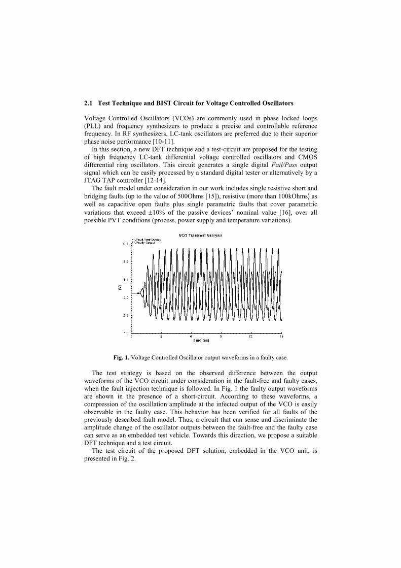
Fig. 1. Voltage Controlled Oscillator output waveforms in a faulty case.
The test strategy is based on the observed difference between the output waveforms of the VCO circuit under consideration in the fault-free and faulty cases, when the fault injection technique is followed. In Fig. 1 the faulty output waveforms are shown in the presence of a short-circuit. According to these waveforms, a compression of the oscillation amplitude at the infected output of the VCO is easily observable in the faulty case. This behavior has been verified for all faults of the previously described fault model. Thus, a circuit that can sense and discriminate the amplitude change of the oscillator outputs between the fault-free and the faulty case can serve as an embedded test vehicle. Towards this direction, we propose a suitable DFT technique and a test circuit.
The test circuit of the proposed DFT solution, embedded in the VCO unit, is presented in Fig. 2.

Fig. 2. The VCO along with the proposed test circuit.
In this configuration two pairs of PMOS/NMOS “sensing” transistors (M7/M5 and M6/M8) sink a certain amount of current, which depends on the output oscillation voltages. The gates of each pair of sensing transistors are directly connected to the output nodes of the VCO. Two tailing current mirrors (M11/M12 and M9/M10), are driven by the first pair of the “sensing” transistors (M7/M5). Accordingly, the second pair of sensing transistors (M6/M8) drives the other pair of mirrors (M13/M14 and M15/M16). In the fault-free case the current mirrors have been suitably adjusted so that, the currents of M11/M12 and M13/M14 dominate over these generated by the mirrors M9/10 and M15/16, driving the nodes S1 and S2 towards ground. In the contrary case of a fault existence, the current of the mirrors M9/10 or M15/16 dominates over that generated by the mirrors M11/M12 or M13/M14, rising the node S1 or S2 towards Vdd, and providing a fault indication signal.
Fig. 3. Response of the test circuit in a faulty case.
In the presence of a fault, the compression of the amplitude, on at least one of the oscillator outputs, results in a reduction of the current that flows through the corresponding PMOS “sensing” transistor (M7 or M6). Consequently the corresponding NMOS current mirror (M11/M12 or M13/M14) fails to discharge its dedicated node (S1 or S2) and thus the output of the corresponding buffer (BUF-1 or BUF-2) remains high, indicating fault detection as shown in Fig. 3.
In order to demonstrate the effectiveness of the proposed DFT scheme, the topology has been designed using a 0.35μm Si-Ge BiCMOS technology. The DFT scheme has been evaluated for the hard faults, while its effectiveness in the presence of soft faults has also been validated. The fault coverage results are summarized in Table 1. As it can be observed in this table, the DFT scheme is highly effective presenting an overall fault coverage performance of 91.8%.
Table 1. Fault coverage results for the BIST-VCO.
Fault Type Fault Coverage (%) Drain opens (DO) (4/4) 100 Gate opens (GO) (4/4) 100 Source open (SO) (4/4) 100 Gate to Drain sorts (GDS) (3/3) 100 Gate to Source shorts (GSS) (4/4) 100 Drain to Source shorts (DSS) (4/4) 100 Varactor-Inductor opens (VIO) (6/10) 60 Inductor shorts (IS) (2/2) 100 Varactor shorts (VS) (2/2) 100 VCO Output shorts (OS) (4/4) 100 Inductor variations (IV) ±10% (4/4) 100 Varactor variations (VV) ±10% (4/4) 100 Overall Fault coverage (45/49) 91.8
2.2 Test Technique and BIT Circuit for Low Noise Amplifiers
A test technique for Low Noise Amplifiers along with the accompanied build-in circuit has also been proposed in the present work. The proposed BIT is capable to detect faults related to output amplitude alterations (attenuations or over-amplifications) and discriminate faulty from fault free LNA circuits (both differential and single ended), without deteriorating the overall performance of the circuit under test [17-20]. The fault model under consideration in this work includes parametric faults (passive and active devices’ parameter deviations outside specified limits) as well as catastrophic faults (resistive and capacitive opens, resistive shorts between devices’ terminals and resistive bridgings between circuit nodes).
The DLNA-BIT topology outline is presented in Fig. 4. The BIT circuit is driven directly from the outputs of the DLNA and provides a single digital PASS/FAIL signal. It consists of two main subcircuits: a) the first one is the Amplitude Alterations Detector (AAD) and b) the second is the Timing Difference Discriminator (TDD). The first subcircuit monitors the outputs of the DLNA and provides two digital
signals, TEST1 and TEST2, which perform a transition from VDD to ground. In case of output amplitude alterations, due to a fault in the CUT, the two response signals of AAD present a relative transition timing difference. The second subcircuit detects the existence or not of those timing differences and discriminates faulty from fault free circuits.
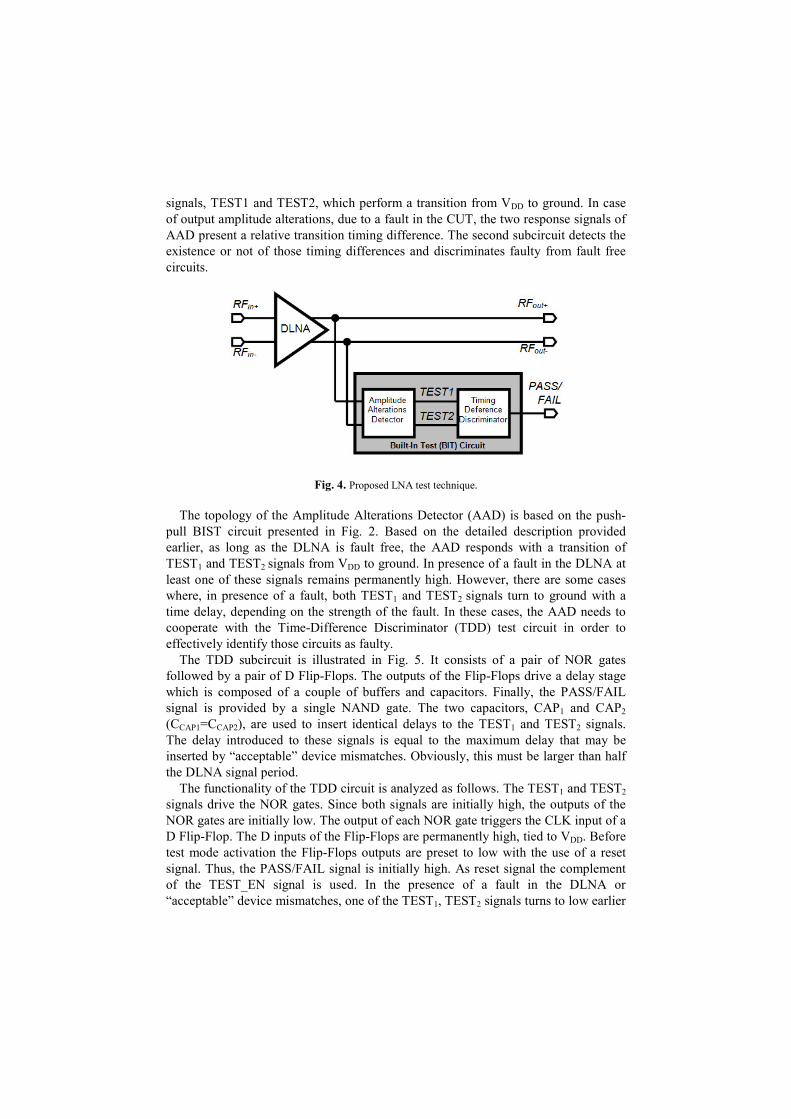
Fig. 4. Proposed LNA test technique.
The topology of the Amplitude Alterations Detector (AAD) is based on the push-pull BIST circuit presented in Fig. 2. Based on the detailed description provided earlier, as long as the DLNA is fault free, the AAD responds with a transition of TEST1 and TEST2 signals from VDD to ground. In presence of a fault in the DLNA at least one of these signals remains permanently high. However, there are some cases where, in presence of a fault, both TEST1 and TEST2 signals turn to ground with a time delay, depending on the strength of the fault. In these cases, the AAD needs to cooperate with the Time-Difference Discriminator (TDD) test circuit in order to effectively identify those circuits as faulty.
The TDD subcircuit is illustrated in Fig. 5. It consists of a pair of NOR gates followed by a pair of D Flip-Flops. The outputs of the Flip-Flops drive a delay stage which is composed of a couple of buffers and capacitors. Finally, the PASS/FAIL signal is provided by a single NAND gate. The two capacitors, CAP1 and CAP2 (CCAP1=CCAP2), are used to insert identical delays to the TEST1 and TEST2 signals. The delay introduced to these signals is equal to the maximum delay that may be inserted by “acceptable” device mismatches. Obviously, this must be larger than half the DLNA signal period.
The functionality of the TDD circuit is analyzed as follows. The TEST1 and TEST2 signals drive the NOR gates. Since both signals are initially high, the outputs of the NOR gates are initially low. The output of each NOR gate triggers the CLK input of a D Flip-Flop. The D inputs of the Flip-Flops are permanently high, tied to VDD. Before test mode activation the Flip-Flops outputs are preset to low with the use of a reset signal. Thus, the PASS/FAIL signal is initially high. As reset signal the complement of the TEST_EN signal is used. In the presence of a fault in the DLNA or “acceptable” device mismatches, one of the TEST1, TEST2 signals turns to low earlier

than the other. Without loss of generality, let us consider that this is the TEST1 signal. Consequently, the output of the corresponding NOR1 gate rises to high triggering the pertinent Flip-Flop. The output of the Flip-Flop goes high and the same stands for the Delayed_TEST1 signal after a time delay that is determined by the capacitance value attached to it. The Delayed_TEST1 signal drives the second NOR gate. Depending on the delay time for the falling edge of the TEST2 signal, with respect to TEST1, the second Flip-Flop may be also triggered or not. In the first case, the falling edge of the TEST2 arrives earlier than the rising edge of the Delayed_TEST1 signal (this is a small delay on TEST2 related to device mismatches). Then, the output of the NOR2 gate goes high (since both TEST2 and Delayed_TEST1 signals are low) and the second Flip-Flop is triggered raising its output to high. Consequently, both inputs of the NAND gate are permanently high resulting in a low PASS/FAIL response which indicates that the DLNA is fault free. In the second case, the falling edge of the TEST2 signal arrives later than the rising edge of the Delayed_TEST1 signal (this is a greater delay on TEST2 related to a fault in the DLNA). Then, the output of the corresponding NOR2 gate remains permanently low and the same stands for the output of the related Flip-Flop. Consequently, the second input of the NAND gate is low and the PASS/FAIL signal remains high indicating the presence of the fault in the DLNA.
Fig. 5. The Timing Difference Discriminator.
Simulations on a typical DLNA, designed in a 0.35μm Si-Ge BiCMOS technology, have demonstrated an overall fault coverage of the proposed test technique and the BIT circuit over 90%. The fault coverage results are summarized in Table 2. The proposed test technique can be applied in either single ended or differential Low Noise Amplifiers. Moreover the test circuit offers a high fault coverage at the expense of a very low silicon area cost. Consequently, suspicious LNA circuits can be easily identified early in the production cycle (e.g. at the wafer or die level) reducing the total manufacturing cost.
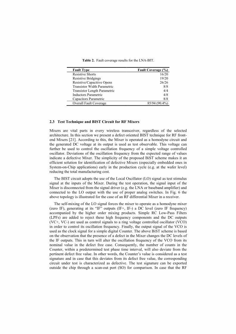
Table 2. Fault coverage results for the LNA-BIT.
Fault Type Fault Coverage (%) Resistive Shorts 16/20 Resistive Bridgings 19/20 Resistive/Capacitive Opens 26/26 Transistor Width Parametric 8/8 Transistor Length Parametric 4/4 Inductors Parametric 4/8 Capacitors Parametric 8/8 Overall Fault Coverage 85/94 (90.4%)
2.3 Test Technique and BIST Circuit for RF Mixers
Mixers are vital parts in every wireless transceiver, regardless of the selected architecture. In this section we present a defect oriented BIST technique for RF front-end Mixers [21]. According to this, the Mixer is operated as a homodyne circuit and the generated DC voltage at its output is used as test observable. This voltage can further be used to control the oscillation frequency of a simple voltage controlled oscillator. Deviations of the oscillation frequency from the expected range of values indicate a defective Mixer. The simplicity of the proposed BiST scheme makes it an efficient solution for identification of defective Mixers (especially embedded ones in System-on-Chip applications) early in the production cycle (e.g. at the wafer level) reducing the total manufacturing cost.
The BIST circuit adopts the use of the Local Oscillator (LO) signal as test stimulus signal at the inputs of the Mixer. During the test operation, the signal input of the Mixer is disconnected from the signal driver (e.g. the LNA or baseband amplifier) and connected to the LO output with the use of proper analog switches. In Fig. 6 the above topology is illustrated for the case of an RF differential Mixer in a receiver.
The self-mixing of the LO signal forces the mixer to operate as a homodyne mixer (zero IF), generating at its “IF” outputs (IF+, IF-) a DC level (zero IF frequency) accompanied by the higher order mixing products. Simple RC Low-Pass Filters (LPFs) are added to reject these high frequency components and the DC outputs (VC+, VC-) are used as control signals to a ring voltage controlled oscillator (VCO) in order to control its oscillation frequency. Finally, the output signal of the VCO is used as the clock signal for a simple digital Counter. The above BiST scheme is based on the observation that the presence of a defect in the Mixer changes the DC levels of the IF outputs. This in turn will alter the oscillation frequency of the VCO from its nominal value in the defect free case. Consequently, the number of counts in the Counter, within a predetermined test phase time interval, will also deviate from the pertinent defect free value. In other words, the Counter’s value is considered as a test signature and in case that this deviates from its defect free value, the corresponding circuit under test is characterized as defective. The test signature can be exported outside the chip through a scan-out port (SO) for comparison. In case that the RF
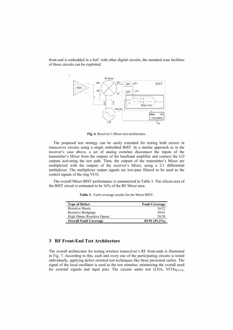
front-end is embedded in a SoC with other digital circuits, the standard scan facilities of those circuits can be exploited.
Fig. 6. Receiver’s Mixer test architecture.
The proposed test strategy can be easily extended for testing both mixers in transceiver circuits using a single embedded BiST. In a similar approach as in the receiver’s case above, a set of analog switches disconnect the inputs of the transmitter’s Mixer from the outputs of the baseband amplifier and connect the LO outputs activating the test path. Then, the outputs of the transmitter’s Mixer are multiplexed with the outputs of the receiver’s Mixer, using a 2:1 differential multiplexer. The multiplexer output signals are low-pass filtered to be used as the control signals of the ring VCO.
The overall Mixer-BIST performance is summarized in Table 3. The silicon area of the BIST circuit is estimated to be 16% of the RF Mixer area.
Table 3. Fault coverage results for the Mixer-BIST.
Type of Defect Fault Coverage Resistive Shorts 16/22 Resistive Bridgings 39/41 High Ohmic Resistive Opens 28/28 Overall Fault Coverage 83/91 (91.2%)
3 RF Front-End Test Architecture
The overall architecture for testing wireless transceiver’s RF front-ends is illustrated in Fig. 7. According to this, each and every one of the participating circuits is tested individually, applying defect oriented test techniques like those presented earlier. The signal of the local oscillator is used as the test stimulus, minimizing the overall need for external signals and input pins. The circuits under test (LNA, VCOsRX-TX,
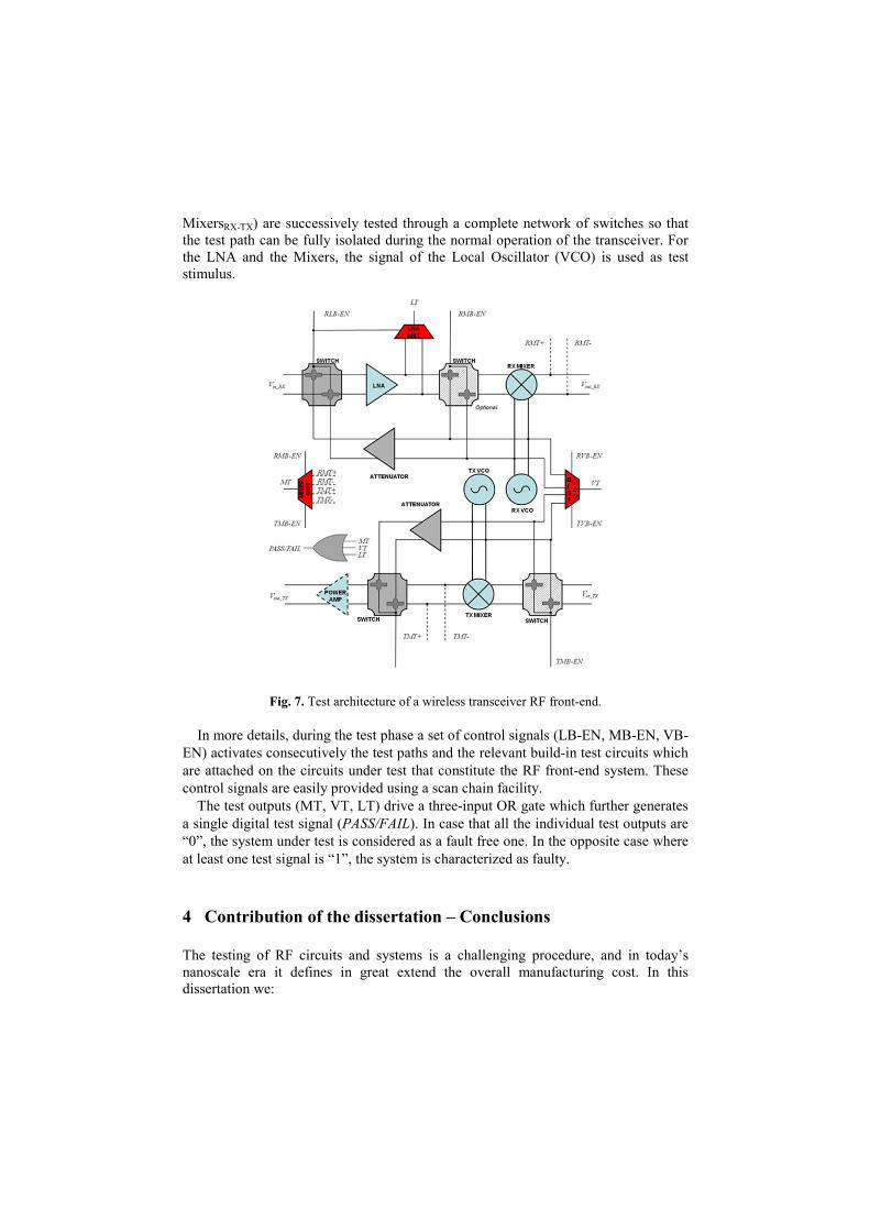
MixersRX-TX) are successively tested through a complete network of switches so that the test path can be fully isolated during the normal operation of the transceiver. For the LNA and the Mixers, the signal of the Local Oscillator (VCO) is used as test stimulus.
Fig. 7. Test architecture of a wireless transceiver RF front-end.
In more details, during the test phase a set of control signals (LB-EN, MB-EN, VB-EN) activates consecutively the test paths and the relevant build-in test circuits which are attached on the circuits under test that constitute the RF front-end system. These control signals are easily provided using a scan chain facility.
The test outputs (MT, VT, LT) drive a three-input OR gate which further generates a single digital test signal (PASS/FAIL). In case that all the individual test outputs are “0”, the system under test is considered as a fault free one. In the opposite case where at least one test signal is “1”, the system is characterized as faulty.
4 Contribution of the dissertation – Conclusions
The testing of RF circuits and systems is a challenging procedure, and in today’s nanoscale era it defines in great extend the overall manufacturing cost. In this dissertation we:

Proposed a novel technique for testing wireless transceiver’s RF front-end circuits, based on a defect oriented approach. The resulted overall architecture can efficiently utilize the available digital and analog system resources during the test phase (for cost reduction) and effectively distinguish the defective from the defect-free structures.
Developed defect oriented design for testability circuits for the basic modules that constitute the RF front-end of the wireless transceivers (LNA, Mixers, VCOs).
Based on the results obtained from the analysis, this dissertation does not only answer the question “Can the RF system testing get more effective and cost efficient?” but it goes one step further, to the more fundamental, “Is it worthwhile to test RF systems?”, and the answer is, yes.
As future work, a defect-oriented approach for testing transmitter’s RF amplifiers may be considered as well as a technique for self-calibration of the defective circuits, in order to increase manufacturing yield.
References
1. Milor, L.S.: A Tutorial Introduction to Research on Analog and Mixed-Signal Circuit Testing. In: IEEE Transactions on Circuits and Systems – II: Analog and Digital Signal Processing, vol. 45, no. 10, pp. 1389—1407 (1998).
2. Akbay, S.S., Halder, A., Chatterjee, A., Keezer, D.: Low-Cost Test of Embedded RF/Analog/Mixed-Signal Circuits in SOPs. In: IEEE Transaction on Advanced Packaging, vol. 27, no. 2, pp. 352—363 (2004).
3. Variyam, P., Cherubal, S., Chatterjee, A.: Prediction of Analog Performance Parameters using Fast Transient Testing. In: IEEE Trans. on Computer-Aided Design of Integrated Circuits and Systems, vol. 21, no. 3, pp. 349—361 (2002).
4. Voorakaranam, R., Cherubal, S., Chatterjee, A.: A Signature Test Framework for Rapid Production Testing of RF Circuits. In: IEEE Design Automation and Test in Europe Conference, pp. 186-191 (2002).
5. Bushnell, M. L., Agrawal, V. D.: Essentials of Electronic Testing for Digital, Memory and Mixed-Signal VLSI Circuits. Kluwer Academic Publishers (2001).
6. Slamani, M., Kaminska, B.: Multifrequency Analysis of Faults in Analog Circuits. In: IEEE Design and Test of Computers, vol.12, no. 2, pp.70-80 (1995).
7. Huang, J.-L., Ong, C.-K., Cheng, K.-T.: A BIST Scheme for On-Chip ADC and DAC Testing. In: Proc. of the Design Automation and Test in Europe Conference (DATE), pp. 216—220 (2000).
8. Dabrowski, J., Gonzalez-Bayon, J.: Mixed Loop-back BIST for RF Digital Transceivers. In: Proc. of the International Symposium on Defect and Fault Tolerance in VLSI Systems (DFT), pp. 220—228 (2004).
9. Yoon, J-S., Eisenstadt, W.R.: Embedded Loopback Test for RF ICs. In: IEEE Trans. on Instrumentation and Measurement, vol. 54, no.5, pp. 1715—1720 (2005).
10.Craninckx, J., Steyaert, M.: A fully integrated CMOS DCS-1800 frequency synthesizer. In: Proc. of IEEE Dig. Tech. Papers, pp. 372—373 (1998).
11.Rofougaran, A., Rael, J., Rofougaran, M., Abidi, A.: A 900 MHz CMOS LC-oscillator with quadrature outputs. In: Proc. of IEEE Int. Solid-State Circuits Conference (ISSCC), pp. 392--393 (1996).
12.Dermentzoglou, L., Tsiatouhas, Y., Arapoyanni, A.: A Design for Testability Scheme for CMOS LC-Tank Voltage Controlled Oscillators. In: Journal of Electronic Testing: Theory and Applications, vol. 20, no. 2, pp. 133—142 (2004)
13.Dermentzoglou, L., Tsiatouhas, Y., Arapoyanni, A.: A novel scheme for testing radio frequency voltage controlled oscillators. In: 10th IEEE International Conference on Electronics, Circuits and Systems 2003 (ICECS 2003), pp. 595—598 (2003)
14.Dermentzoglou, L., Tsiatouhas, Y., Arapoyanni, A.: A built-in self-test scheme for differential ring oscillators”, 6th International Symposium on Quality of Electronic Design, 2005 (ISQED 2005), pp. 448—452 (2005)
15.Tang, J.J., Lee, K.J., Liu, B.D.: A Practical Current Sensing Technique for IDDQ Testing. In: IEEE Transactions on VLSI Systems, vol. 3, no. 2, pp. 302—310 (1995).
16.Variyam, P.N., Chatterjee, A.: Digital-Compatible BIST for Analog Circuits Using Transient Response Sampling. In: IEEE Design & Test of Computers, pp. 106—115 (2000).
17.Dermentzoglou, L., Arapoyanni, A., Tsiatouhas, Y.: A Built-In-Test Circuit for RF Differential Low Noise Amplifiers. In: IEEE Transactions on Circuits and Systems I, Vol 57, no. 7, pp. 1549-1558 (2010)
18.Dermentzoglou, L., Tsiatouhas, Y., Arapoyanni, A.: A Design for Testability Technique for Differential RF Low Noise Amplifiers. In: XX Conference on Design of Circuits and Integrated Systems (DCIS 2005)
19.Dermentzoglou, L., Tsiatouhas, Y., Arapoyanni, A.: An Embedded Test Circuit for RF Single Ended Low Noise Amplifiers. In: 14th IEEE International Conference on Electronics, Circuits and Systems, (ICECS 2007), pp. 1119—1122 (2007)
20.Dermentzoglou, L., Tsiatouhas, Y., Arapoyanni, A., Karagounis, A.: A Built-In Test Circuit for Single Ended RF Low Noise Amplifier. In: 17th North Atlantic Test Workshop (NATW 2008)
21.Dermentzoglou, L., Tsiatouhas, Y., Arapoyanni, A.: A Build-In Self-Test Technique for RF Mixers. In: 13th IEEE International Symposium on Design and Diagnostics of Electronic Circuits and Systems (DDECS2010), pp. 88—92 (2010)
Related Documents


