ELSEVIER Materials Science and Engineering B34 (1995) 83-105 MATERIALS SCIENCE & ENGINEERING B Critical review A critical review of ohmic and rectifying contacts for silicon carbide Lisa M. Porter, Robert F. Davis Department of Materials Science and Engineering, North Carolina State University, Raleigh, NC 27695-7907, USA Received 10 May 1995 Abstract For more than three decades, SiC has been investigated as a wide band gap semiconductor. This paper reviews ohmic and rectifying metal contacts on n- and p-type ~- and fl-SiC reported throughout that time period. Electrical characteristics, Schottky barrier heights (SBHs), thermal stability, and chemical reactions are discussed. Most metals formed very good rectifying contacts in the as-deposited condition on both n- and p-type 6H-SiC with Schottky barrier heights ~>1 eV. Low ideality factors (n < 1.1) and high breakdown voltages (> 1100 V) have been displayed in this material. The electrical properties of contacts on 3C-SiC have been more dependent on the quality of the 3C-SiC films, which have been plagued by higher defect densities than 6H-SiC. In general, a partial pinning of the Fermi level has been evidenced by positive correlations, which are less than 1 (~0.2-0.6), between the SBHs and the metal work functions. Ohmic contacts with low contact resistivities (~< 10 -5 f~ cm2), especially important for high power applications, on any of the SiC polytypes have been exceptionally difficult to achieve. Most of the ohmic contacts have relied on high doping concentrations in combination with annealing at temperatures between 800 and 1300 °C. Annealed Ni and A1 have primarily been used in ohmic contact metallizations for n- and p-type SiC, respectively. The tendency of SiC to react with metals to form carbides and/or silicides at potential device operating temperatures (~ 600 °C) can be a problem for potential long term applications at high temperature. These critical issues are discussed along with future perspectives for research approaches. Keywords: Silicon carbide; Semiconductors; Ohmic metal contacts; Rectifying metal contacts I. Introduction In certain close-packed materials such as SiC, there exists a one-dimensional type of polymorphism called polytypism. Polytypes are alike within the closest- packed planes but differ in the stacking sequence in the dimension perpendicular to these planes. The stacking sequence of these closest-packed planes is commonly described by an ABC notation. In SiC each letter refers to a bilayer composed of individual layers of Si and C. A repetitive ABC stacking sequence yields the zinc blende structure. This is the only cubic SiC polytype and is referred to as 3C- or fl-SiC, where the 3 refers to the number of Si/C bilayers in the periodic sequence. The hexagonal (wurtzite) (ABAB...) sequence is also found in SiC. Both can also occur in more complex, intermixed forms yielding a wider range of ordered, larger period, hexagonal (H) or rhombohedral (R) structures of which 6H-SiC is the most common. In 0921-5107/95/$09.50 © 1995 -- Elsevier Science S.A. All rights reserved SSDI 0921 -5107(95)01276-1 actuality, this polytype is only 33% hexagonal. Its ABCACB stacking sequence consists of two (identical neighboring) hexagonal bilayers and four (different neighboring) cubic bilayers. All of these noncubic struc- tures are known collectively as a-SiC. The multitude of extreme thermal and electronic properties of SiC produces numerous and novel combi- nations of attributes for a semiconductor material for both optoelectronic and for high-power, -frequency, -temperature, -speed, and radiation hard microelec- tronic devices. The great potential of (6H)-SiC as a semiconductor in such electronic device applications is challenged by the difficulty of controlling metal contact properties. These properties of the metal/SiC interfaces include uniformity and thickness of the interfacial region, sta- bility at high temperatures (~ 600 °C), and most impor- tantly, the Schottky barrier height (SBH), or the energy barrier for electrons traversing the interface.

Welcome message from author
This document is posted to help you gain knowledge. Please leave a comment to let me know what you think about it! Share it to your friends and learn new things together.
Transcript

E L S E V I E R Materials Science and Engineering B34 (1995) 83-105
MATERIALS SCIENCE &
ENGINEERING
B
Critical review
A critical review of ohmic and rectifying contacts for silicon carbide
Lisa M. Porter, Robert F. Davis Department of Materials Science and Engineering, North Carolina State University, Raleigh, NC 27695-7907, USA
Received 10 May 1995
Abstract
For more than three decades, SiC has been investigated as a wide band gap semiconductor. This paper reviews ohmic and rectifying metal contacts on n- and p-type ~- and fl-SiC reported throughout that time period. Electrical characteristics, Schottky barrier heights (SBHs), thermal stability, and chemical reactions are discussed. Most metals formed very good rectifying contacts in the as-deposited condition on both n- and p-type 6H-SiC with Schottky barrier heights ~> 1 eV. Low ideality factors (n < 1.1) and high breakdown voltages (> 1100 V) have been displayed in this material. The electrical properties of contacts on 3C-SiC have been more dependent on the quality of the 3C-SiC films, which have been plagued by higher defect densities than 6H-SiC. In general, a partial pinning of the Fermi level has been evidenced by positive correlations, which are less than 1 (~0.2-0.6), between the SBHs and the metal work functions. Ohmic contacts with low contact resistivities (~< 10 -5 f~ cm2), especially important for high power applications, on any of the SiC polytypes have been exceptionally difficult to achieve. Most of the ohmic contacts have relied on high doping concentrations in combination with annealing at temperatures between 800 and 1300 °C. Annealed Ni and A1 have primarily been used in ohmic contact metallizations for n- and p-type SiC, respectively. The tendency of SiC to react with metals to form carbides and/or silicides at potential device operating temperatures (~ 600 °C) can be a problem for potential long term applications at high temperature. These critical issues are discussed along with future perspectives for research approaches.
Keywords: Silicon carbide; Semiconductors; Ohmic metal contacts; Rectifying metal contacts
I. Introduction
In certain close-packed materials such as SiC, there exists a one-dimensional type of polymorphism called polytypism. Polytypes are alike within the closest- packed planes but differ in the stacking sequence in the dimension perpendicular to these planes. The stacking sequence of these closest-packed planes is commonly described by an ABC notation. In SiC each letter refers to a bilayer composed of individual layers of Si and C. A repetitive ABC stacking sequence yields the zinc blende structure. This is the only cubic SiC polytype and is referred to as 3C- or fl-SiC, where the 3 refers to the number of Si/C bilayers in the periodic sequence. The hexagonal (wurtzite) ( A B A B . . . ) sequence is also found in SiC. Both can also occur in more complex, intermixed forms yielding a wider range of ordered, larger period, hexagonal (H) or rhombohedral (R) structures of which 6H-SiC is the most common. In
0921-5107/95/$09.50 © 1995 - - Elsevier Science S.A. All rights reserved
SSDI 0921 -5107(95)01276-1
actuality, this polytype is only 33% hexagonal. Its ABCACB stacking sequence consists of two (identical neighboring) hexagonal bilayers and four (different neighboring) cubic bilayers. All of these noncubic struc- tures are known collectively as a-SiC.
The multitude of extreme thermal and electronic properties of SiC produces numerous and novel combi- nations of attributes for a semiconductor material for both optoelectronic and for high-power, -frequency, -temperature, -speed, and radiation hard microelec- tronic devices.
The great potential of (6H)-SiC as a semiconductor in such electronic device applications is challenged by the difficulty of controlling metal contact properties. These properties of the metal/SiC interfaces include uniformity and thickness of the interfacial region, sta- bility at high temperatures ( ~ 600 °C), and most impor- tantly, the Schottky barrier height (SBH), or the energy barrier for electrons traversing the interface.

L.M. Porter, R .F Davis / Materials" Science and Engineering B34 (1995) 83 105 84
Table 1 Selected structural, thermal, and electronic properties of 6H- and 3C-SiC at 300 K
Property 6H-SiC Ref. 3C-SiC Ref.
Band gap Lattice parameter
Work function
Electron affinity
Electron mobility
Saturated electron drift velocity Breakdown electric field Dielectric constant
Thermal conductivity
Eg = 3.0 eV [31 2.3 eV [3] a = 3.08086 A [116] a - 3.08269/k [116] c= 15.1174 A e = 7.55124/~ ~s = 4.75 + / - 0.10 eV [12] ~s ~ 5.2 eV calculated (n-type, (0001) surface): from Xs 4.85 + / - 0.10 eV (p-type, value (0001) surface) Zs = 3.3 eV calculated Zs - 4.0 eV [12,117]
from [12] /~n-700cm 2 (Vs) I (at n= [118] /Ln=980cm 2 (Vs) t (at n [119] 1.1 x 1016cm 3) =4.0× 1016cm 3) vs~,t = 2.0 x 107 cm s i [120] Usa t = 2.5 x 107 cm S i [121]
E R = 4 x 10⁶Vcm i [122] E B - 3 × 10⁶Vcm i [122]
~:1(0) = 10.03 [123] ~:(0) = 9.72 [1231 c±(0) = 9.66 c(,z) = 6.52 ~;11(3c) = 6.70 ~:±(oc) = 6.52 ~rT=4.9Wcm I deg-t [124] aT--4.9Wcm --Ideg ; [124]
The Schot tky bar r i e r height de te rmines the electr ical behav io r o f an ohmic or Scho t tky contact . A n ohmic contact , i m p o r t a n t for m a k i n g outs ide c o m m u n i c a t i o n to a device, is defined as having: (1) a l inear and symmetr ic c u r r e n t - v o l t a g e re la t ionship for posi t ive and negat ive voltages; and (2) negligible resistance com- pa red with the bulk o f the device. Therefore , a low SBH is necessary to create a good ohmic contact . However , a large SBH is necessary to create a good Schot tky , or rectifying, contact . A rect ifying con tac t a l lows current to flow for only one sign (posi t ive or negat ive) o f vol tage bias, thereby becoming a c o m p o - nent o f the active region o f the device.
Because of the cri t ical impor t ance o f the SBH (also wri t ten symbol ica l ly as ~B), much research has been devo ted to achieving an unde r s t and ing o f the under ly- ing phenomena , its cont ro l , and the exper imenta l p ro- cess routes by which the la t ter m a y b e achieved. When two mater ia l s come in contact , the respective Fe rmi levels must align. In 1938 M o t t [1] defined a re la t ion- ship which is now known as the Schot tky M o t t l imit for an ideal metal s emiconduc to r contact . This rela- t ionsh ip s tates tha t (for an n- type semiconduc tor ) the bar r ie r height is equal to the work funct ion o f the meta l , ~M, minus the e lect ron affinity o f the semicon- duc tor , Zs
(1)B = ( ~ M - - XS (1)
This re la t ionship implies tha t con t ro l over the ba r r i e r height is achieved by the choice o f metal .
In pract ice , however , it is c o m m o n l y found tha t ~B is ei ther weakly dependen t on or independen t o f ¢~M. This
empir ica l devia t ion f rom the S c h o t t k y - M o t t l imit led to the deve lopmen t o f a theory based on surface states ra ther than work funct ion differences [2]. Because the surface o f a mater ia l is i tself an imperfect ion, surface states can exist within the energy gap o f the bulk semiconductor . Bardeen found tha t the densi ty o f sur- face states can be so high tha t they prede te rmine the bar r ie r height, such that ~B is comple te ly independent of q~M- In this case the bar r ie r height or the Fe rmi level is said to be ' p inned ' , and cont ro l over the bar r ie r height is lost. Usual ly the ac tual re la t ionship between ~B and ~ u falls somewhere between the Schot tky Mor t l imit and the Bardeen limit.
In add i t i on to the electronic in terac t ions at an ' int i- ma te ' m e t a l - s e m i c o n d u c t o r contact , the chemical and s t ructura l in terac t ions mus t be considered. Mos t bar r ie r height models do not address chemical bonds at the interface, yet few interfaces con ta in mater ia l s which are inert with respect to each other. The s t ructure may be i m p o r t a n t in terms o f affecting the number of surface (interface) states, which in turn affects the var iabi l i ty o f the bar r ie r height.
2. Important properties of silicon carbide
Table 1 lists some of the s t ructural , thermal , and electronic p roper t i e s o f c~(6H)-SiC and f l(3C)-SiC. The band gaps o f the 6H and 3C po ly types at r o o m temper- a ture are ~ 3 . 0 and ~2 .3 eV, respectively [3]. Different ra t ing systems for semiconductors , dependen t on the pa r t i cu la r opera t ing specifications, have been deve loped
L.M. Porter, R.F. Davis / Materials Science and Engineering B34 (1995) 83-105 85
as "figures of merit." Johnson's figure of merit [4], (EBVsat/TC) 2 is based on high frequency and high power operation in discrete devices. Keyes' figure of merit [5], av(Vs,t/e) 1/2 considers high speed operation in devices in integrated circuits. Thus, both a high breakdown elec- tric field, EB, and a high saturated electron drift veloc- ity, Vsat, are desired for high frequency/power operating conditions. In the case of SiC, it is the high breakdown field which gives it a high rating. A high thermal conductivity, aT, is needed to dissipate heat quickly from small, closely-spaced devices. The conductivity of SiC is superior to that of Cu at room temperature. Baliga's figure of merit [6], (g,t/Eg 3) is based on the need to minimize conduction losses in power field effect transistors (FETs). Here e is the dielectric constant of the semiconductor,/z is the electron mobility, and Eg is the band gap. Baliga later developed a figure of merit for high frequency applications which accounts for switching losses [7], (/,tEBZV~°5/(2VBI'5)), where V~ is the gate drive voltage and VB is the breakdown voltage. These four figures of merit for a few semiconductors are normalized with respect to Si in Table 2. The very high figures of merit for 6H-SiC combined with the ability to grow boules and films as well as dope the material both n- and p-type make it a distinguished wide band gap semiconductor. The reader is referred to Refs. [8-11] for detailed descriptions of properties and technological status of SiC and other wide band gap semiconductors.
Two other properties of the semiconductor which are important in terms of contacts are work function and electron affinity. Pelletier et al. [12] measured under ultra high vacuum conditions the work function of n- and p-type 6H-SiC as a function of temperature be- tween 300 and 1600 K, and from these measurements the electron affinity may be calculated. The n-type material was doped with N and the p-type material with A1. Special attention was given to cleaning the surface so as not to introduce extrinsic surface states caused by impurities. The normally Si-terminated (0001) surfaces were heated to T~< 1230°C. Higher
Table 2 Figures of merit calculated for selected semiconductor materials ratioed to silicon: Johnson's figure of merit (JFM), Keyes' figure of merit (KFM), Baliga's figure of merit (BFM), and Baliga's high frequency figure of merit (BHFFM)
Material JFM [115] KFM [115] BFM [7,125] BHFFM [7,125]
Si 1.0 1.0 1.0 1.0 GaAs 7 0.456 13 10 InP 16 0.608 l0 7 GaN 282 1.76 910 100 6H-SiC 695 5.12 106 13 3C-SiC 1137 5.8 40 12 Diamond 8206 32.2 8574 454
temperatures were not used in order to avoid the forma- tion of excess carbon on the surface as a result of Si eyaporation. However, heat treatment at those tempera- tures should still leave a C-rich surface according to [13].
The work function remained constant for each do- pant type within the temperature range measured. In addition, the difference in work functions between n- and p-type samples (4.75 and 4.85 eV, respectively) was small. These results led to the conclusion that the Fermi level is pinned at the surface due to intrinsic surface states. However, if the surfaces were graphite termi- nated, as is likely for surface states may have than intrinsic.
The electron affinity,
the temperatures used, these been extrinsic in nature rather
which is closely related to the work function, was also calculated by this group. Using the method of Frese [14], where Zs = O s - 0.5Eg, the room temperature electron affinity was calculated to be 3.7eV. However, using the intrinsic work function value of 4.80 eV and subtracting 1.5 eV, which is half of the band gap, a value of 3.3 eV is obtained. Because the 3.3 eV value follows from the measured work function of Pelletier et al., it has been used in the present research as the electron affinity of 6H-SiC to calculate predicted Schottky barrier heights. Any error in Zs simply shifts all of the theoretical barrier heights by the same amount and, therefore, does not affect the slope of • B vs. OM. While the room temperature work func- tion was not measured for 3C-SiC, the room tempera- ture electron affinity was reported to be 4.0 eV. Using the method stated above, this would correspond with a work function of 5.2 eV for intrinsic fl-SiC.
3. Surface chemistry
As the preparation of a clean semiconductor surface is critically important to the resulting contact proper- ties, this section briefly reviews the various cleaning procedures used on SiC, the resulting chemistry and structure of the surface, and associated problems.
Preparation of a chemically-clean, atomically-ordered surface has proven to be a nontrivial problem in SiC. The surface chemistry and structure of single crystals of the e (6H) polytype were first investigated in 1975 by van Bommel et al. [13]. The surfaces were monitored with low energy electron diffraction (LEED) and Auger electron spectroscopy (AES) after exposure to various temperatures under ultra high vacuum (UHV) condi- tions. As a result of low temperature heating (at 250 °C) for an unspecified amount of time, the Si-termi- nated (0001) surface exhibited a _x/3 × ~/3 LEED pat- tern, while the C-terminated (0001) surface exhibited a 1 x 1 pattern. A 6x/3 × 6x/3, R30 ° pattern began to develop on the (0001) face during successive 15min anneals at 800 °C; this became the only pattern after

86 L.M. Porter, R.F. Davis / Materials Science and Engineering B34 (1995) 83 105
heat treatment at 1000 °C. As a result of annealing at 1500 °C the surface exhibited a 1 x 1 graphite phase. The (000]-) face showed 2 x 2 or 3 x 3 patterns after 800 and 1000 °C. After 1500 °C graphite rings appeared on this latter face, indicative of polycrystalline graphite.
The surfaces after the 800 °C exposure showed AES C peaks of the carbide type. After 1000 °C the Si-to-C ratio decreased, and the C peak changed from carbidic to graphitic. These two results, along with the develop- ment of a peak at 20 eV, indicated the formation of graphite.
The LEED results at 250 °C were interpreted by van Bommel et al. as being representative of reconstructed surfaces with possible submonolayer impurities. The 6x/3, 30 ° pattern was attributed to the SiC substrate with a monocrystalline graphite top layer, which had rotated 30 ° with respect to the underlying SiC lattice. Thus, under the UHV conditions used by these investi- gators graphite begins to form at the (0001) surface as low as 800 °C. Graphite formation occurred at lower temperatures on the (000i) surface. On both faces the mechanism was reported to consist of the collapse of three C layers to form one graphite layer due to the incongruent evaporation of Si. Many orientations are possible, but apparently only one is favored on the Si-face.
Following the work of van Bommel, researchers have experimented with methods to clean the SiC surface without forming a graphitic surface layer. Kaplan and Parrill [15] heated fl-SiC (100) and 6H-SiC (0001) and (000i) samples at progressively higher temperatures, typically for 3 min, in the presence of a Ga flux to volatilize the surface oxide. The oxide was reduced at temperatures as low as 850 °C; however, complete re- moval was a very slow process below 1050°C. In addition, temperatures which resulted in complete re- moval of oxygen also resulted in a decrease of the Si/C ratio. After annealing at 1185 °C for 3 rain, the Si/C ratio decreased significantly, and the data indicated the initial formation of graphite. In fl-SiC C2 x 2 struc- tures were observed by LEED, which were in agree- ment with the results of Dayan [16] for comparable temperatures. The C-face of 6H-SiC displayed 1 x 1 patterns, except after extended heating at 900 °C, when some areas displayed a x/3 x x/3 reconstruction. The Si-face displayed a 3 × 3 reconstruction.
The residual, tenacious oxide was thought to be located in regions of the surface where oxygen can penetrate well into the surface defects. Therefore, com- plete oxide removal on rough surfaces should be more difficult. Although the surface oxide was volatilized by the Ga, the temperatures required to completely remove the oxide resulted in the same problem of graphite termination.
In later work [17] Kaplan heated SiC in the presence of an elemental Si flux, which removed the surface
oxide as volatilized SiO. Prior to this step and to loading into the UHV chamber, the samples were chemically cleaned successively in detergent solution, trichloroethylene, acetone, and methanol. Some sam- ples were also dipped in hydrofluoric acid followed by deionized water, but this treatment did not noticeably affect the amount of residual oxide. The 6H-SiC (0001) and fl-SiC (111) surfaces were indistinguishable. Faint satellite spots appeared with a small amount of oxide still present. After heat treatment at 850, 950, and > 1000 °C, the LEED patterns were 3 x 3; (x/3 x x/3), R30°; and 1 x 1, respectively. The Si surface concentra- tion decreased with temperature. Parallel electron en- ergy loss spectroscopy (PEELS) revealed the beginning of graphite segregation at 950 °C. The 3 x 3 phase was asserted to correspond with an adsorbed Si bilayer with a high vacancy concentration. Annealing at 950 °C depleted the surface Si and caused the surface recon- struction to change to a x/3 x x/3 phase. Additional annealing at > 1000 °C resulted in continual depletion of surface Si, and the development of a corresponding 1 x 1 pattern. The 1 x 1 phase was attributed to a range of surface chemistries and defect structures. As would be expected from the above model, with the continued Si depletion the amount of graphitic C increased. The initial appearance of the 1 x 1 phase was believed to be due to the elimination of the Si adlayer resulting in defects. By comparison, the work of van Bommel ex- hibited a direct change from x/3 x x/3 to a graphitic state without first exhibiting a 1 x 1 phase.
In order to more efficiently remove the oxide at low temperatures, metals which form vapor phase oxides with more negative free energies than O bound to Si are worth considering as an extension of the experiments with Ga and Si. A promising candidate might be A1, which readily forms vapor phase oxides (A10 and A120) and which may be easily evaporated from the surface. Other possible choices are Mg or Ca.
Bozso et al. [18] investigated the Si-terminated (0001) surface of 6H-SiC crystals using X-ray photoelectron spectroscopy (XPS) and X-ray and electron excited Auger spectroscopy. Prior to these analytical studies, the crystals were dipped into concentrated aqueous HF, rinsed in distilled H20, and cleaned in acetone and propyl alcohol. The major residual contaminants left were fluorine and oxygen. After the chemical clean the samples were exposed to a combination of low angle ( ~ 80 ° angle of incidence) argon ion sputtering (500 eV) and high temperature annealing. Fluorine and oxygen remained after this treatment at 800 °C for 40 min but were removed at 1000 °C for 2 min. However, Ar was still present, but was eventually eliminated after pro- longed heating. An atomically clean surface was achieved, and preferential removal of Si or C was not observed. However, possible surface damage due to the sputtering process was not reported. The resulting state

L.M. Porter, R.F. Davis / Materials Science and Engineering B34 (1995) 83-105 87
of the surface should be further investigated before this preparation technique is employed for metal contacts, as defect states can pin the Fermi level. If the annealing prevents surface damage, this technique may be a viable solution to the surface cleaning problem.
The Si- and C-faces of a mixture of 6H and 15R polytypes were investigated after cleaning and disorder- ing by Ar ion sputtering (similar conditions as above) and subsequent annealing [19]. In agreement with the previous study [18], the Si/C ratio remained constant. Changes did occur with heat treatment to ~ 1000 °C, which caused a decrease in the XPS C (Is) binding energy. The Si (2p and 2s) binding energies remained constant. These results indicated a change in the C chemistry. Examination of the peak areas revealed an increase in the C/Si ratio on the C-face between 630 and 830 °C and a substantial increase on both faces above 1030 °C. The C enrichment was much higher on the C-face. These results were reaffirmed by the AES analyses. Electron energy loss spectra indicated the formation of graphite at ~ 900 °C.
While in the latter two studies 500 eV Ar ions were used in the sputtering process, Andreev et al. [20] sputtered oxidized (0001) and (0001) surfaces of 6H-SiC with 640 eV electrons at a flux density of 2 -5 x 10¹⁷ e/ (cm 2 s). The sample temperature was between 700 and 1000 °C. Electrons were used instead of ions because of their low mass and, hence, lower tendency to damage the SiC surface. Auger analysis showed that this proce- dure resulted in an uncontaminated, stoichiometric sur- face. However, it was stated that graphitization occurred when the procedure was continued after the oxide was removed. Although evidence was not given, the surface was reported to have been undamaged. Considering the chemical and microstructural results along with the experimental process, this cleaning pro- cedure may be a viable technique if the equipment is available and the parameters are carefully controlled.
A chemical and thermal cleaning process [21], which would be more easily implemented for commercial devices, was developed in conjunction with the fabrica- tion and characterization of Schottky contacts on SiC. Oxidized 6H-SiC (0001) surfaces were first etched in a 10% HF aqueous solution. Thermal oxidation was found to be a critical step for leaving a non-C-rich surface. Hydrocarbons were the main contaminant left on the surface after the etching step, as shown by the minor peak component on the high binding energy side of the C ls XPS peak (Fig. 1). After heating the samples in a vacuum system (base pressure ~ 1 - 5 x l0 9 Torr) at 700 °C for 15 min, these hydrocar- bons were removed from the surface, while residual O and a trace amount of F were still present. As illus- trated in Fig. 2, XPS was also used to determine the amount of band bending before and after deposition of various metal contacts. After these cleaning steps an
(b) C ls
f t
f .: .......... Before 700°C desorption .," : ..... After 700°0 desorption . ~ / , ," ~ ~ ~
. , ? '
I . . . . I . . . . I . . . . . . "
295 290 285 280 Binding Energy (eV)
Fig. 1. XPS C ls spectra of 6H-SiC (0001) after 10 min in 10% HF followed by a deionized water rinse. The minor peak attributed to hydrocarbons was removed after heating at 700 °C for 15 min in UHV [21].
upward band bending of a few tenths of an electron- volt was calculated, indicating the presence of surface states.
Evidence for the absence of surface states in the band gap under different conditions has been reported by Parrill and Bermudez [22]. Alpha SiC, of unspecified polytype and undetermined Si or C termination, was chemically cleaned in acetone, methanol, 30s in concen- trated aqueous HF, and a final rinse in methanol followed by annealing at 850-950 °C in a Si-flux. All of the oxygen was removed, but the surfaces did contain excess Si. The excess Si was removed by annealing for 1-2 min at temperatures ranging from 960 to 1160 °C. The surface showed a 1 x 1 LEED pattern after anneal- ing in the Si flux. Subsequent heating at ,~ 1160 °C gave a 3 x 3 reconstruction and no graphite formation ac- cording to Auger analysis. Data was collected only from the 1 x 1 surface (Si-rich surface) since 3 x 3 surfaces were not uniform. The bulk valence band was studied by using high energy photons (Mg K~, 1253.6eV) for which the photoelectron attenuation length is ~7 monolayers in the valence band. The
Ec J E F . . . . . . . . - j
E v
EC is J
>o
J Fig. 2. Energy band diagram of 6H-SiC showing the relationship between • B and the binding energies measured by XPS. Prior to metal deposition, the value of • B was calculated to be 0.40 + 0.1 eV [21].

88 L.M. Porter, R.F. Davis' / Materials Science and Engineering B34 (1995) 83 105
surface valence band was investigated using low energy photons (Zr M-zeta, 151.4 eV) for which the attenua- tion length is ~2.5 monolayers. The photoemission results showed no states within the optical band gap; however, they do suggest that surface states exist below the valence band edge.
The evidence seems to indicate that certain adatom terminations (e.g. Si or O) on the (0001) or (0001) surface of a-SiC result in a reasonably low or the absence of surface states within the band gap. In the case of the partial monolayer of oxygen, there appears to be a sufficient density of surface states to reduce the index of behavior, defined as the slope of the plot of the barrier height vs. metal work function, from 1.0 but which is insufficient to actually completely pin the Fermi level (shown in later sections). An index of behavior of 1.0 for a particular semiconductor indicates that the Fermi level is unpinned, and the Schottky barrier heights follow the ideal behavior predicted by the Schottky Mott relationship.
Other work [23] does indicate that there is some pinning due to intrinsic C vacancies, which vary in concentration with polytype. The barrier heights of Cr on many different SiC polytypes were compared with the theoretically predicted behavior of vacancies on the surface of a semiconductor. Carbon-terminated surfaces were prepared by chemical cleaning, which was not described, and then heated in vacuum at 600 °C for 1 h. The barrier height correlated well with the degree of hexagonality for several hexagonal and rhombohedral polytypes. Although the band gap varies similarly, the Fermi level did not sit at a constant value of the band gap, as would occur if this were purely a function of band gap. As the concentration of vacancies increased, the barrier height decreased. (The barrier height of Cr/6H-SiC was 1.1-1.2 eV.) The report claims that carbon vacancies form a level at the surface in the upper half of the band gap and that a higher concentra- tion of carbon vacancies causes a greater shift of Ev towards E c. Compar ing this theory with SBH results presented later, one might conclude that intrinsic prop- erties (vacancies) of SiC may cause some gap states at the surface, but the specific details of the surface and its preparat ion will be the final factor in determining the density of surface states and where they are located.
4. Contacts to ~-silicon carbide
4.1. Schottky contacts to or-SiC
4. I. 1. n-type a-SiC Some of the early investigations of Schottky contacts
on n-type ~(6H)-SiC (summarized in Table 3) were performed in 1964 by Mead and Spitzer [24]. In this report barrier heights for metals on SiC and other
elemental Group IV and I I I - V semiconductors were found to be nearly independent of work function. Al- though the work functions of Au and A1 differ by ~0.8 eV, their resulting barrier heights on SiC were 1.95 and 2.0 eV, respectively. It was reported that for most Group IV and III V semiconductors where both vacuum cleavage and chemical preparation could be employed, the barrier heights resulting from the two preparation techniques were the same; however, it was not specified if both processes were used for SiC. There- fore, it cannot be concluded whether the results can be attributed to the surface preparation.
Subsequently, Hagen [25] also found q~B on a-SiC crystals, comprised of the 6H and 15R polytypes, to be independent of qb M. The barrier height on n-type sam- ples was 1.45 eV for Au, Ag, and A1. In addition, q~B for Au contacts on etched (0001) surfaces was the same as that on cleaved (IT00) surfaces. The former surfaces were etched in a molten s o d a - b o r a x mixture, rinsed with deionized water, treated with an HF solution, again rinsed with deionized water and kept in methanol until placed in the vacuum system. It was concluded that the Fermi level is fixed by surface states at the middle of the band gap.
Notable results were reported for Au contacts ther- mally evaporated (base pressure < 10 6 Torr) on n-type 6H-SiC (0001) [26]. The C-terminated surfaces were cleaned with concentrated HF, etched in molten sodium peroxide, rinsed in dilute HC1 and deionized water and then dipped in methanol and dried with N2. The semi- logarithmic current vs. voltage plot extends over seven orders of magnitude with an ideality factor of n = 1.07. The calculated barrier height of 1.45 eV was in agree- ment with that of Hagen [25] for Au on the Si-termi- nated (0001) surface.
Platinum, Au, Ag, Ni, Cr, and A1 sputtered on 6H-SiC produced rectifying contacts [27]. Surfaces were etched in a mixture of potassium hydroxide and sodium nitrate in ratios ranging from 1:4 to 1:100 at 477- 577 °C. However, the carrier type and orientation of the SiC were not indicated. Depending on the metal and the surface preparation, the band bending at the semiconductor surface ranged from 0.6 to 2.5 eV. Alu- minum evaporated in vacuum (10 ~'Torr) on n-type SiC was characterized after heat treatment by another group [28]. The substrates were etched in molten KOH. The resulting oxide was then etched by dipping in HF followed by deionized water. Prior to the A1 deposition Ni was deposited on the back and annealed for 3 min at 1200 °C in an Ar ambient to create an ohmic contact. After the AI was deposited (vacuum pressure 10 6 Torr) the samples were annealed in an Ar ambient for 3 min at 660 °C (m.p. of A1), 770 and 900 °C. Before annealing, the AI contacts showed high leakage currents. After annealing, the leakage decreased ( ~ 2 × 10 2 A c m 2 at - 5 V ) , and the ideality factor

L.M. Porter, R.F. Davis / Materials Science and Engineering B34 (1995) 83 105 89
T a b l e 3 Rec t i fy ing c o n t a c t s o n n - type ~ (6H o r mixed) -S iC. O n l y those s tudies wh ich r e p o r t e d S B H s a re l isted here fo r brevi ty . T h e su r face p r e p a r a t i o n s w h i c h cons i s t ed o f a t least a su r f ace ox ide e t ch ing s tep a n d a h y d r o c a r b o n r e m o v a l s tep b y h e a t i n g in h igh o r u l t r a - h i g h v a c u u m were r ea ted as ' ve ry g o o d ' . T h o s e w h i c h cons i s t ed o f a t least a c h e m i c a l c lean a n d a su r f ace ox ide e t ch ing s tep bu t l acked the capab i l i t y fo r h e a t i n g in h igh v a c u u m were r a t e d as ' g o o d ' . Th i s r a t i n g sys t em is b a s e d o n ana lyses o f the SiC su r face b y X P S
Metalliza- Deposition Deposition Deposition Annealing ~ a (eV) SiC Method of Origin of Surface Ref. tion method temperature pressure (Torr) condition surface qb ameas . SiC preparation
Au NR NR NR none 1.95 NR C - V NR A1 NR NR NR none 2.0 NR C - V NR Au thermal evap. RT ~ 1 0 9 none 1.45 (1i00) C - V , PR NR
Ag thermal evap. RT ~ 1 0 9 none 1.45 (1i00) C V, PR NR
AI thermal evap. RT ~ 10 9 none 1.45 (1100) C-V, PR NR
Au thermal evap. NR < I0 6 b.p. none 1.40 (000T) C-V , PR, subl. I - V
AI thermal evap. NR 10 -6 to 900 °C, ~ 1.7 (0001) C - V Acheson 3 min
Ti e-beam evap. RT 10 io b.p. none 0.84-0.88 (0001) I -V, C-V , XPS
Ti e-beam evap. RT 10- io b.p. 700 °C, 0.86-1.04 (0001) l -V , C - V 40-60 min
Pd thermal evap. RT 10 to b.p. none 1.60-1.62 (0001) I -V, C V, 1.11 (0001) and XPS
Au thermal evap. RT 10 io b.p. none 1.14-1.19 (0001) I -V, C - V , CVD 1.37-1.40 (0001) and XPS
Ag thermal evap. RT 10 io b.p. none 1.10 (0001) l -V , C V, CVD 0.83-0.92 (0001) and XPS
Mn thermal evap. RT 10 - l ° b.p. none 0.79 0.81 (0001) I -V , C V, CVD and XPS
AI thermal evap. RT 10 lo b.p. none 0.84-0.89 (000I) I V, C -V , CVD 0.26-0.30 (0001) and XPS
Mg thermal evap. RT 10 ~o b.p. none 0.33 (0001) I - V and XPS CVD 0.30-0.34 (0001)
Pt sputtered 140 °C NR none 1.04-1.10 NR I V and C - V
Ti thermal evap. RT 10 lo b.p. none 1.0-1.03 (000T) 1 V, C-V , 0.73 (0001) and XPS
Ti thermal evap. RT 10 1o b.p. 400 °C 0.98 (000I) I V, C V, 0.93 0.97 (0001) and XPS
Ni thermal evap. RT 10 ~o b.p. none 1.54 1.68 (000i) I V, C V, 1.24 1.29 (0001) and XPS
Ni thermal evap. RT 10 ~o b.p. 400°C, 1.51-1.66 (000i) I V, C - V , 30s 1.23-1.25 (0001) and XPS
Ni thermal evap. RT 10 - I ° b.p. 600 °C, 1.16-1.39 (0001) I -V, C-V , 30 s and XPS
AI thermal evap. RT 10 io b.p. none 0.84 0.89 (0001) l -V , C V, 0.26-0.30 (0001) and XPS
AI thermal evap. RT 10 ~o b.p. 600 °C, 1.36-1.66 (000T) I V, C-V , 30s 0.82-1.12 (0001) and XPS
Au thermal evap. RT NR none 1.4 (000T) I - V
Pt e-beam evap. RT 10 ~o b.p. none 1.06 1.33 (0001) I - V and XPS
Pt e-beam evap. RT 10 1o b.p. 450 750 °C, 1.15-1.26 (0001) I - V 20 min
H f e-beam evap. RT 10 ~o b.p. none 0.97 (0001) I V and C - V
Hf e-beam evap. RT 10 ~o b.p. 700 °C, 1.01-0.86 (0001) l V and C V 20 60 min
Co e-beam evap. NR 10 7 none 0.79 (0001) 1-V and C V
Co e-beam evap. RT 10 ~o b.p. none 1.06-1.15 (0001) l -V , C V, and XPS
Ni e-beam evap. RT 10 ~o b.p. none 1.14-1.21 (0001) I - V and C V
seeded sub.; CVD epi seeded sub.; CVD epi CVD
seeded sub.; CVD ept seeded sub.; CVD e D seeded sub.; CVD epl seeded sub.; CVD e D seeded sub.; CVD e D seeded sub.; CVD ep~ seeded sub.; CVD epi seeded sub.; CVD epi Acbeson substr.; CVD epl seeded sub.; CVD eD seeded sub.; CVD ept seeded sub.; CVD epl seeded sub.; CVD e D seeded sub.; CVD ep~ seeded sub.; CVD epl seeded sub.; CVD e D
NR [24] NR [24] cleaved in [25] v a c .
cleaved in [25] vac. cleaved in [25] vac. good [26]
good [28]
very good [21,30,34]
very good [21,30,34]
very good [32]
very good [32]
very good [32]
very good [32]
very good [32]
very good . [32]
NR [441
very good [33]
very good [33]
very good [33]
very good [33]
very good [33]
very good [33]
very good [33]
good [45]
very good [34,36]
very good [34,36]
very good [34]
very good [34]
good [90,126]
very good [35]
very good [43]
OB = S c h o t t k y b a r r i e r he ight ; N R = n o t r epo r t ed ; R T = r o o m t e m p e r a t u r e ; b .p . = base p ressure ; sub. = subs t ra te ; epi = epi layer ; I V = c u r r e n t - vo l t age ; C V = c a p a c i t a n c e vo l tage ; X P S = X - r a y p h o t o e l e c t r o n s p e c t r o s c o p y .

90 L.M. Porter, R.F. Davis / Materials Science and Engineering B34 (1995) 83 105
Fig. 3. High resolution TEM image of as-deposited Ti/6H-SiC. The boxed-in region in the upper part of the image is magnified in the lower part of the image. The arrow at the interface marks the position of a step in the SiC surface. The misfit dislocations which are marked with lines, did not extend all the way to the interface. After Ref. [21].
was 2.0-2.3. The built-in voltage was 1.7 V after an- nealing at 900 °C. It is likely that annealing the SiC at 1200 °C prior to deposition of A1 depleted some of the surface Si, which in turn may have caused leaky con- tacts. Reaction of A1 with the excess C very likely occurred during post-deposition annealing and resulted in lower leakage currents. The lower temperatures should not be sufficiently high to activate A1 in SiC and create a p-type surface layer.
Titanium films deposited by UHV electron beam evaporation at room temperature onto n-type 6H-SiC (0001) grew epitaxially and displayed rectifying behav- ior [21,29 31]. Both Ti ( a = 2 . 9 5 A , c = 4 . 6 8 / k ) and 6H-SiC (a = 3.08 A, c = 15.11 A) have hexagonal crys- tal structures, corresponding to a - 4 % lattice mis- match between the close packed planes. Fig. 3 shows a high resolution TEM image of this nearly ideal inter- face. The misfit dislocations did not extend to the interface, and therefore, the Ti film was considered pseudomorphic. Surfaces were cleaned in a solution of ethanol/hydrofluoric acid/deionized water (10:1:1) fol- lowed by a 700 °C thermal desorption in UHV. Analy- sis of unannealed, thin (4-12/k) Ti films by XPS indicated Ti C bonding at the Ti/SiC interface. The
leakage currents of thicker 1000 ~) films were as low a s 9 x l 0 8 A c m 2a t - 1 0 V , and theideali ty factors were between 1.01 and 1.09. The contacts remained stable after annealing at 700 °C for 1 h, which resulted in a thin, crystalline TiC layer at the SiC interface and TisSi 3 in the remainder of the reacted region. Barrier heights before and after annealing were 0.88 and 1.04 eV, respectively. The change in barrier height is attributed to the chemical reaction, which created a new metal/SiC interface.
From the results of I V, C-V, and XPS analyses, Waldrop et al. [32] have calculated the barrier heights of Pd, Au, Ag, Tb, Er, Mn, A1, and Mg deposited at room temperature on the Si- and/or C-faces of n-type 6H-SiC. The metals were deposited in UHV by evapo- ration from W wire baskets. Prior to the depositions the substrates were RCA cleaned, oxidized, etched in HF, and desorbed at 600 °C under UHV conditions. It was estimated that ~ 1/2 monolayer oxygen remained on the C-face and ~3/4 on the Si-face. A relatively large barrier height variation resulted. With the exclu- sion of the rare earth elements, in general there was an increase in q)~ with q~M. This trend is displayed in Fig. 4, where the SBHs calculated from the three techniques

L.M. Porter, R.F. Davis / Materials Science and Engineering B34 (1995) 83 105 91
are plotted vs. the work functions of the metals and compared to the theoretical SBHs according to the S c h o t t k y - M o t t limit. Three linear fits to the three sets of data points are also shown. The slopes, S, of these lines, often referred to as the index of interface behavior, give a quantitative indication of how closely the system follows S c h o t t k y - M o t t behavior (i.e. how close S is to 1). As is evident from Fig. 4, the index of interface behavior may depend on the technique used to measure the SBHs. In this case S varied from 0.47 to 0.63. These results give evidence for a partial pinning of the Fermi level in 6H-SiC. While not shown in the figure, the barrier heights of the rare earth elements, Er and Tb, ranged from 1.61 to 2.18 eV calculated from C - V measurements and 1.04 to 1.41 eV calculated from I - V measurements.
Barrier heights of unannealed and annealed Ni, Ti, and A1 were later measured by the same group on n-type 6H-SiC [33]. These data points are also included in Fig. 4. X-ray photoelectron spectroscopy analyses indicated the formation of TiC and TiSi~ in the unannealed Ti/SiC interface region. No chemical reactions were detected on the Si-face before or after annealing Ni/SiC at 400 °C.
In addition to the Ti contacts described in a previous paragraph, Porter et al. [34-36] have also studied the chemistry and microstructure along with the electrical properties and SBH's of other metal/SiC systems. The SBHs calculated f rom I - V , C - V , and XPS analyses of Ti, Pt, HI', Co, and Ni contacts are shown in Fig. 5. The slopes S vary from 0.12 for the data points calcu- lated from I - V measurements to 0.40 and 0.41 for those calculated from C - V and XPS measurements, respectively. While these slopes are somewhat less than those derived from Waldrop 's data, both sets of results show a significant, positive correlation between SBH and metal work function and a susceptibility to mea- surement technique. Differences due to processing should be minimal since similar cleaning and deposition procedures and substrate material were used in both
2.5-
I -I- theoretical • ", measured (I-V) I
2 . 0 - 0 measured (XPS) ~- 0 measured (C-V) . -
S=l;O..- _=z 15- . - - " ~s=047 <c-v)
~, 1 . 0 - o ~ ~ '~ E
S-0.62 (XPS)
o.5- . - ~ s=o.6s 0-v)
0 . 0 -
Metal Work Function (eV)
F ig . 4. D a t a p o i n t s o f e x p e r i m e n t a l l y - d e t e r m i n e d a n d t h e o r e t i c a l
barrier heights on n-type 6H-SiC (000l) vs. work function of the metal contacts. The experimental data points are from Waldrop et al. [32,33]. The slopes, S, of the linear fits through each set of data points are indicated.
2.5-
I - l . . theoretical I .e Zx measured (I-V) I S=1.0 , ' "
2 . 0 - 0 measured (C-V) . - ' " A o • > 0 measured (XPS 1 •
o ~- 1 . 5 - - • S=0.41
• 1- o ° .~_ 1 . 0 - ~ 2 ZX P_
0 . 5 -
0 . 0 - I I
3.5 4.0 4.5 510 515 610 Metal Work Function (eV)
Fig. 5. Data points of experimentally-determined and theoretical barrier heights on n-type 6H-SiC (0001) vs. work function of the metal contacts. The experimental data points are from Porter et al. [21,34-36,43]. The slopes, S, of the linear fits through each set of data points are indicated.
studies. The main difference in the two sets of results occurs between the calculations based on I - V measure- ments and XPS. This result is quite interesting consider- ing that I - V measurements are very dependent on the homogeneity of the interface [37-41]. The lower slopes in the former set of data are believed to be partly due to the particular metals studied. For example, the Pt contacts yielded a significantly lower SBH calculated from I - V measurements than that calculated from XPS analyses, a result attributed to inhomogeneity of the interface [36].
In this latter study the increase in grain size and grain orientation with the temperature of the anneal was accompanied by an increase in the SBH calculated from I - V measurements. The samples were successively an- nealed for 20 rain at 450, 550, 650, and 750 °C. No re- action occurred at temperatures below 750 °C. The first reaction phases, crystalline PtzSi and an amorphous C phase, formed after annealing at 750 °C. This interfa- cial reaction was proposed to reduce any adherence problems associated with Pt contacts. These contacts displayed low ideality factors (n < 1.1) and typical leak- age currents of 5 × 10 - S A c m 2 a n d 2 × 10 8Acre -2 at - 1 0 V before and after annealing, respectively.
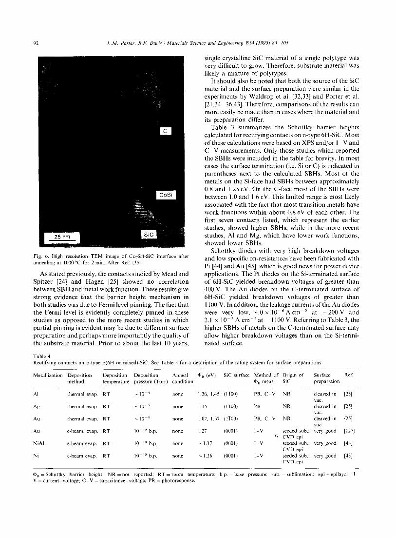
Cobalt contacts [35] deposited at room temperature also formed excellent rectifying contacts with ideality factors and reverse leakage currents similar to the Pt contacts. However, annealing at 800 °C for 20 min re- suited in a substantial increase in the leakage currents, while ohmic-like behavior was displayed after annealing at 1000 °C for 2 min. Analysis of the latter contacts revealed that extensive reaction occurred resulting in the formation of CoSi and graphite. This reaction resulted in a highly irregular interface, as shown in Fig. 6. Nickel, which reacts with SiC at even lower tempera- ture [42] and is chemically similar to Co, is commonly used as an ohmic contact to n-type SiC and may also form a highly irregular interface after annealing.
92 L.M. Porter, R.F. Davis / Materials Science and Engineering B34 (1995) 83 105
Fig. 6. High resolution TEM image of Co/6H-SiC interface after annealing at 1000 °C for 2 min. After Ref. [35].
As stated previously, the contacts studied by Mead and Spitzer [24] and Hagen [25] showed no correlation between SBH and metal work function. These results give strong evidence that the barrier height mechanism in both studies was due to Fermi level pinning. The fact that the Fermi level is evidently completely pinned in these studies as opposed to the more recent studies in which partial pinning is evident may be due to different surface preparat ion and perhaps more importantly the quality of the substrate material. Prior to about the last 10 years,
single crystalline SiC material of a single polytype was very difficult to grow. Therefore, substrate material was likely a mixture of polytypes.
It should also be noted that both the source of the SiC material and the surface preparation were similar in the experiments by Waldrop et al. [32,33] and Porter et al. [21,34 36,43]. Therefore, comparisons of the results can more easily be made than in cases where the material and its preparation differ.
Table 3 summarizes the Schottky barrier heights calculated for rectifying contacts on n-type 6H-SiC. Most of these calculations were based on XPS and/or I V and C - V measurements. Only those studies which reported the SBHs were included in the table for brevity. In most cases the surface termination (i.e. Si or C) is indicated in parentheses next to the calculated SBHs. Most of the metals on the Si-face had SBHs between approximately 0.8 and 1.25 eV. On the C-face most of the SBHs were between 1.0 and 1.6 eV. This limited range is most likely associated with the fact that most transition metals have work functions within about 0.8 eV of each other. The first seven contacts listed, which represent the earlier studies, showed higher SBHs; while in the more recent studies, A1 and Mg, which have lower work functions, showed lower SBHs.
Schottky diodes with very high breakdown voltages and low specific on-resistances have been fabricated with Pt [44] and Au [45], which is good news for power device applications. The Pt diodes on the Si-terminated surface of 6H-SiC yielded breakdown voltages of greater than 400 V. The Au diodes on the C-terminated surface of 6H-SiC yielded breakdown voltages of greater than 1100 V. In addition, the leakage currents of the Au diodes were very low, 4 . 0 x 10 6 A c m 2 at - 2 0 0 V and 2.1 x 10 3 A cm 2 at - 1100 V. Referring to Table 3, the higher SBHs of metals on the C-terminated surface may allow higher breakdown voltages than on the Si-termi- nated surface.
Table 4 Rectifying contacts on p-type ~(6H or mixed)-SiC. See Table 3 for a description of the rating system for surface preparations
Metallization Deposition Deposition Deposition Anneal q~B (eV) SiC surface Method of Origin of Surface Ref. method temperature pressure (Torr) condition q~B meas. SiC preparation
A1 thermal evap. RT ~ 10 9 none 1.36, 1.45 (1100) PR, C V NR cleaved in [25] vac.
Ag thermal evap. RT ~10 9 none 1.15 (1100) PR NR cleaved in [25] v a c ,
Au thermal evap. R T ~10 9 none 1.07, 1.37 (1100) PR, C V NR cleaved in [25] v a c ,
Au e-beam, evap. RT 10 io b.p. none 1.27 (0001) I V very good [127]
NiA1 e-beam evap. RT 10 io b.p. none ~ 1.37 (0001) 1 V very good [43]
Ni e-beam evap. R T 10 to b.p. none ~ 1.36 (0001) I V very good [43]
seeded sub.; '~ CVD epi
seeded sub.; CVD epi seeded sub.; CVD epi
q~B=SChottky barrier height; N R = n o t reported; R T - r o o m temperature; b . p . - b a s e pressure; sub. =subl imat ion; epi=epi layer ; I V = current voltage; C - V - capacitance voltage; PR = photoresponse.

L.M. Porter, R.F. Davis / Materials Science and Engineering B34 (1995) 83-105 93
4.1.2. p-type a-SiC Table 4 summarizes the limited number of Schottky
contacts on p-type a-SiC found in the literature and their calculated SBHs. These studies were not as exten- sive as many of those performed for Schottky contacts on n-type SiC.
Gold and A1 on p-type samples produced SBHs of 0 .9 -1 .25eV and 1.30-1.47eV, respectively [25]. The higher SBH of A1 compared with Au on p-type material would be expected considering the lower work function of the former.
Our measurements on p-type SiC have shown consis- tent differences from measurements on n-type material. The SBHs tend to be higher on p-type than on n-type 6H-SiC. While leakage currents for Au, NiA1, and Ni contacts on p-type 6H-SiC (0001) were comparable with those on n-type 6H-SiC, the ideality factors were higher (n ~ 1.1-2.1). These higher ideality factors indi- cate that thermionic emission is not the dominant current transport mechanism. Deep level transient spectroscopy (DLTS) will probably be used to deter- mine whether recombination at deep levels accounts for the electrical behavior of the contacts on p-type material.
4.2. Ohmic contacts to c~-SiC
4.2.1. n-type e-SiC The earliest work found in the literature on ohmic
contacts to n-type a-SiC was performed in 1970 on Cr and Cr alloys [46]. The remainder of the work has been confined within the past few years. In the former case the main concerns were to form ohmic contacts which were both ductile and oxidation resistant and had low resistance. The contacts described were Cr or Cr alloys (at least 5 wt.%) with Fe, Ni, or Fe and Ni. To form ohmic contacts the metals were heated to above their respective melting temperatures (1500-1900 °C). These high temperatures assured a significant reaction with the SiC, and very likely created a graded, highly-defec- tive interface associated with the ohmic behavior. Due to the processing requirements and the confinements of size in today 's devices, lower processing temperatures are required.
Although lower annealing temperatures have been used in the more recent work, in most cases the temper- atures have been above 900 °C. The exceptions to this last statement have been in those cases where the SiC was very heavily doped [47,48]. The two exceptions listed in Table 5 along with the other ohmic contacts are the TiN contacts reported by Glass et al. [49,50] and the TiW contacts reported by Crofton et al. [51]. In both cases the ohmic behavior is likely associated with a thin insulating layer. The TiN contacts were de- posited by ion assisted reactive evaporation and an- nealed at 600 °C for 30 min. They were found by XPS
to contain a thin (5-15 A) layer of silicon nitride at the interface, creating a metal insulator semiconductor (MIS) structure. While TiN has a low work function (favorable for an ohmic contact on n-type material), ohmic behavior did not occur in the absence of ion assisted deposition, a process associated with the for- mation of the S i - N layer. This insulating layer was critical to the creation of ohmic contacts but not solely responsible for this behavior, as Pt contacts (high work function) with a S i - N interlayer resulted in rectifying characteristics. It was stated that the insulating layer may act to passivate surface states, resulting in an electron energy band relationship which behaves ac- cording to the Schottky Mott limit. Because the insu- lating layer was so thin, electrons would be able to tunnel through it.
The Ti W (10:90 wt.%) contacts formed ohmic con- tacts after annealing at 600 °C for 5 min following exposure of the SiC surface to an oxygen plasma. Ohmic behavior did not result without the oxygen plasma exposure. It is likely that this process step resulted in the formation of a thin SiO2 layer at the surface, which may be responsible for the ohmic behav- ior by forming a MIS structure similar to that for the TiN contacts.
Annealed Ni has been the most widely used metal for ohmic contacts to n-type SiC. As shown in Table 5, this process generally involves annealing at temperatures above 900 °C. While Crofton et al. reported in an earlier paper [51] a room temperature contact resistivity in the mid 10 2 ~-~ cm 2 range (5 x 10¹⁸ c m - 3 c a r r .
conc.), they were later able to lower this value to less than 9 x 10 - 6 ~ cm 2 (7 9 x 10¹⁸ c m - 3 c a r r . conc.) [52]. The substantial decrease in the calculated contact resis- tivity was partly attributed by the first author (private communication) to a combination of the higher carrier concentration and of the changes in the measurement technique, the annealing conditions, and the processing systems.
Comparably low values (1.7-6 x 10 5 ~ c m 2) were also reported for Ni on 6H-SiC with a 2000/k thick, highly-doped (1-3 x 10 I9 c m 3) 3C-SiC interlayer [53]. The authors attribute the low contact resistivity to the smaller band gap of the 3C polytype. To determine whether the 3C-SiC layer does in fact reduce the barrier height at the 6H-SiC surface, the energy band relation- ship at the interface should be measured.
The lowest values reported to date of contact resistiv- ities of ~< 1 x 10 6 ~ c m 2 [54] have been achieved for annealed (1000°C/5min) Ni on very highly doped (4.5 x 1020 cm 3) n + 6H-SiC (000i). The n + 6H-SiC films were grown by liquid phase epitaxy (LPE) on Acheson-grown 6H-SiC substrates. Silicon nitride was contained in the melt to achieve the notably high N doping levels. Prior to the annealing step, the contact resistivities were greater than 1 x 10 4f~ c m 2.

94 L.M. Porter, R.F. Davis / Materials Science and Engineering B34 (1995) 83 105
T a b l e 5
O h m i c contac t s on n-type c~(6H or mixed)-SiC. See T a b l e 3 f o r a descript ion o f the rating system for surface preparat ions
Metallization Deposition Deposition Deposition Annealing p, ( f l c m 2) SiC carr. conc. SiC Method Origin of method temperature pressure condition (cm 3) surface of p~. SiC
(Torr) mess.
Surface preparation
Ref.
Cr melt ing 10 3 b.p. melt ing N R N R N R
(~>2130 °C)
Ni e-beam N R N R 100M °C/20 s 1.7 x 10 4 4.5 × 10¹⁷ (0001) T L M
evap.
T iN ion-assisted 350°C 10 io b.p. 600°C/30 4 x 10 2 ~1 x 10 ~s (0001) T L M
e-beam min evap.
sputtering R T TiW 10 ~' b.p.
Ni e-beam RT 10 6
evap.
Ni Cr sputtering RT 10 6 b.p.
(60 40 wt.%)
W thermal N R N R
evap.
TiW sputtering R T 10 6 b.p.
Ti thermal RT N R
evap.
Mo sputtering 10 7 b.p. N R
O 2 p l a s m a + 7 . 8 x 1 0 4 4 . 7 x 1 0 ~ (0001)
600 °C/5 min 9 5 0 ° C / 5 m i n mid 10 2 4.7 x 10 ~a (0001)
950°C/5 rain 1.8 × 10 ~ 4.7 x 10 ~8 (0001)
1200 1600°C 5 x 1 0 ~ l x l 0 4 3 x 1 0 1 8 lx l0~ ,~ (0001)
I x 10 2 5 × 10 4 1 x 10 J7 I x 10 ~'; (000i)
7 5 0 ° C / 5 m i n ~ 8 x [0 4 7 8 x I(11~ (0001)
none l x l 0 2 < 2 x 1 0 5 2 x 10¹⁸ 1 × 10 ~° (0001)
none ~ I x 10 4 > l x 10 I~) (000l)
Ta sputtering 10 7 b.p. N.R. none ~1 x 10 4 >1 x 10 a~J (0001)
Ni/3C-SiC resistive N R N R 100M °C/30 s < 1.7 x 10 5 1 2 x 10 as (0001)
evap. < 6 x 10 5 (0001)
Ni e-beam R T 10 (' 950 °C/2 min < 5 × 10 6 7 9 x 10¹⁸ (0001)
evap. (000i)
Ni sputtering N R 10 5 b.p. 1050°C/5 10 3 10 4 9 . 8 x 10¹⁷ (0001)
min W/Ti /Ni sputtering N R 10 s b.p. 1050°C/5 10 3 10 4 9.8 X 10¹⁷ (0001)
min Ni thermal N R N R 1000 °C/5 1 x 10 ~' 4.5 x 10²⁰ (0001)
evap. min Ti-AI thermal N R N R 1000°C/5 <1 x 10 3 4.5 x 102" (000i)
evap. min
circular T L M
four-
point
circular T L M
four- point circular T L M
circular T L M
fotlr-
point
and T L M
four-
point
and T L M
Cox and Strack T L M
T L M
T L M
contact area contact area
N R N R [461
seeded sub.; NR [128]
C V D epi seeded sub. very good [49,50]
seeded sub.: 02 plasma [51]
C V D epi seeded sub.; good [51]
C V D epi seeded sub.; 02 plasma [51]
C V D epi Lely varied [59]
seeded sub.: good [1291
C V D epi seeded sub. good [47]
seeded sub.: good [48]
C V D epi
seeded sub.: good [48]
C V D epi
Lely very good [53]
seeded sub.; good [52]
C V D epi seeded sub. good [130]
seeded sub. good [1301
LPE good [541
LPE good [541
N R = not reported; R T = r o o m temperature: b.p . = base pressure; sub . = subl imat ion: epi = epilayer.
4.2.2. p-type e -S iC It is difficult to form ohmic contacts to p-type mate-
rial by reducing the SBH because o f the large band gap and work function o f SiC. Aluminum is conventionally used in pure form or as an alloy to create ohmic contacts. Annealing the contacts causes A1 to diffuse into the SiC, resulting in an enhanced p-type carrier concentration near the surface. A higher carrier concen- tration corresponds to a narrower depletion region through which holes can effectively tunnel. However, the low melting point and the oxidation characteristics o f AI make processing the contacts difficult. The melt- ing point can be increased by using A1 alloys (e.g. A1-Ti [55 57]), but the extremely high thermodynamic driving force for oxidation o f A1 places strict require- ments on processing and passivating layers.
Table 6 lists a chronology of the various ohmic contacts to p-type c~-SiC. Boron, which is a deep level acceptor in SiC, and A1 were used in the earliest contacts of this type to SiC [58]. The contacts were made by fusing pellets o f A1-Si ( ~ 1:1) or Si with a few percent B to the SiC. This process required tempera- tures o f 1700 °C for the AI-S i and from 1700 to above 2000 °C for the Si-B. It was believed that the enhanced p-type concentration at the SiC surface was formed by recrystallization from solution rather than diffusion of A1 into the SiC. While the temperatures required for these contacts are extremely high, these materials may be more desirable as interlayers, as Si has a significantly smaller band gap than SiC.
Hall [58] also investigated W as an ohmic contact because of its similar thermal expansion coefficient to

L.M. Porter, R.F. Davis/Materials Science and Engineering B34 (1995) 83-105 95
Table 6 Ohmic contacts to p-type ~(6H or mixed)-SiC. Multi-layered contacts are designated with slashes to separate the distinct layers; layers at the surface to the interface with SiC proceed from left to right. See Table 3 for a description of the rating system for surface preparations
Metallization Deposition Deposition Deposition Annealing p~ (~ cm 2)
method temperature pressure condition (Torr)
SiC carr. conc. SiC Method Origin of Surface Ref.
(cm 3) surface of p~ SiC preparation meas.
A l - S i ( ~ 1 : 1 ) melt ing N R 1700°C N R N R (0001) - - Lely N R [58]
S i - B (a few melting N R 1700 2000 N R N R (0001) - - Lely N R [58]
%B) °C
W melting N R 1900 °C N R N R (0001) - - Lely N R [58]
C u - T i melt ing I0 5 > 8 8 0 °C N R N R N R - - Carborun- good [131]
(71:29 at.%) dum Co.
A I - S i melt ing - - 10 5 900-1000 N R N R N R - - Carborun- good [131]
(88.7:I 1.3 at.%) °C d u m Co.
A1-Ti N R N R N R 950 °C/5 N R N R (0001) - - seeded sub.; good [55]
min LPE epi AI e-beam R T 10 6 700 °C/10 1.7 x 10 3 1.8 x 10¹⁸ (0001) T L M seeded sub.; good [51]
evap. min CVD epi W / A u W / W / A I sputtering N R N R 1800 2 5 x 10 4 N R (0001) four- Lely varied [59]
°C/120 s and point (oooT) (0001) AI Ti sputtering R T 10 6b .p . 1000°C/5 2 . 9 × 1 0 2 1.5)<10 5 5 x l 0 t S 2x10¹⁹
min Mo sputtering N R 10 " v b.p. none 2 x 10 4 > l × l019 (0001)
Ta sputtering N R 10 7 b.p. none 7 x 10 4 > 1 x 10¹⁹ {000l)
Ti sputtering N R 10 7 b.p. none 3 × 10 4 > 1 × l0 ~9 (0001)
800°C/10 10 2 - 1 0 -~ 8 × 10¹⁸ (0001)
min 800 850°C 10 2-10 3 8 x 10¹⁸ (0001)
/10 min
950 °C/2 2 - 3 x 10 s N R (0001)
min
450 850 N R >1 x 10 Is N R
°C/20 min 1000 °C/5 N R N R (000i)
min
AI sputter ing N R l0 5 b.p.
W/Pt /At sputtering N R 10 5 b.p.
Ti /AI/C- e-beam N R N R
SiC evap./
L P C V D
Pt e-beam R T 10 m b.p.
evap. Ti/AI thermal N R N R
evap.
circular seeded sub.; good [57]
T L M C V D epi four- seeded sub.; good [48]
point CVD epi and T L M
four- seeded sub.; good [48]
point CVD epi and T L M
four- seeded sub.; good [48]
point CVD epi and T L M
T L M seeded sub. good [130]
T L M seeded sub. good [130]
T L M Lely sub.; very good [53]
LPE epi
seeded sub.; very good [60]
C V D epi Acheson good [54]
sub.; LPE
epi
N R = not reported; R T = r o o m temperature; b.p . = base pressure; sub . = subl imation; epi = epilayer.
SiC. However, annealing these contacts resulted in even greater penetration depth than for the Si alloys.
Two eutectics, C u - T i and A1 Si, were later found to be ohmic after annealing at > 8 8 0 °C and 900-1000 °C, respectively [13]. These annealing temperatures are above the eutectic melting points and resulted in pene- tration o f the contacts in the SiC o f up to 1 pm. Similar penetration depths occurred for the W/AuW/W/A1 con- tacts [59]. These extensive chemical interactions would be devastating in many of today's devices.
As in the case of n-type SiC discussed above, the need for annealing can be reduced or eliminated by heavily doping the surface to create a p + layer in p-type SiC. As-deposited Mo, Ta, and Ti contacts on p + SiC epitaxial films grown by C V D yielded ohmic
contacts [48]. Contact resistivities measured by Kuphal's 4-point method were in the 10 -4 ~ c m 2 range, which was reported to be a conservative value since the method does not account for nonuniform current densi- ties.
The patent by Glass et al. [60] is based on the relationship that the contact resistance decreases with increasing doping concentration and decreasing SBH. When tunneling dominates the current transport, as occurs for high doping concentrations and a finite barrier, the following proportionality holds
Rc oc exp(OB/x/N) (2) where Rc is the specific contact resistance, OB is the Schottky barrier height, and N is the carrier concen-

96 L.M. Porter, R.F. Davis Materials' Science and Engineering B34 (1995) 83 105
Table 7 Rectifying contacts on n-type fl-SiC. The deposition and annealing conditions, calculated Schottky barrier heights, and SiC information are listed for most of the contact metallizations. See Table 3 for a description of the rating system for surface preparations
Metallization Deposition Deposition method temperature
Deposition Annealing qbB(eV ) SiC Method of Origin of Surface pressure condition surface OB means. SiC preparation (Torr)
Ref.
Au e-beam NR 10 7 none; to 500 1.2 (100) C V CVD good [62] evap. °C/1 h
AI thermal RT 10 ¢' b.p. 900°C/3 5 m i n NR (100) CVD good [70] evap.
Au thermal RT 10 ~' b.p. none 1.2 (100) C V CVD good [70] evap.
A1 thermal ~ R T 10 m b.p. none 1.4 (100) XPS CVD Si-rich [67] evap.
Pd thermal RT 10 m b.p. none 0.95, 0.92 (100) XPS, C V CVD very good [63] evap.
Au thermal RT 10 m b.p. none 0.78, 0.87 (100) XPS, C V CVD very good [63] evap.
Co thermal RT 10 m b.p. none 0.69, 0.73 (100) XPS, C V CVD very good [63] evap.
Ti thermal RT 10 m b.p. none 0.53 (100) XPS CVD very good [63] evap.
Ag thermal RT 10 m b.p. none 0.40 (100) XPS CVD very good [63] evap.
Tb thermal RT 10 m b.p. none 0.35 (100) XPS CVD very good [63] evap.
AI thermal RT 10 m b.p. none 0.16 (100) XPS CVD very good [63] evap.
Au thermal RT 10 6 b.p. none vicinal & CVD good [64] evap. off-axis
(100) Ni sputtering NR NR none NR carbonization good [71]
of Si
NR = not reported; RT = room temperature; b.p. = base pressure; XPS = X-ray photoelectron spectroscopy; C V = capacitance voltage.
tration [61]. To reduce the SBH on p-type material, a high work function metal should be used. Although empirical evidence indicates that there is a partial pinning of the Fermi level in 6H-SiC, the SBH has some dependence on metal work function, as shown in Figs. 4 and 5. In this invention ohmic contacts were fabricated by depositing Pt on p-type SiC with a p-t- layer at the surface. Both as-deposited contacts and contacts annealed at tempera- tures to 850 °C displayed ohmic behavior. Platinum has several advantageous properties, including its high melt- ing point and oxidation resistance; however, even its high work function (5.65 eV) is not enough to eliminate the SBH on p-type SiC. For this reason the carrier concen- tration at the SiC surface was increased by ion implan- tation of A1 (at 10kV, 6 x 1015cm 2 dose or 50kV, 2 x 1015 cm 2 dose; 600 °C substrate) and annealing at 1500 °C prior to metallization.
5. Contacts to fl-sil icon carbide
5.1. Schottky contacts to /]-SIC
With the advent of the ability to grow //-SIC thin films in the 1980s came a thrust of research on metal
contacts to this material. However, large concentra- tions of stacking faults, associated with the low stack- ing fault energy of this polytype, as well as twins and threading dislocations occurring in heteroepitaxial films have precluded the achievement o f the predicted electrical properties, both within the semiconductor substrate and at the metal/SiC interface. Table 7 lists the rectifying contacts on n-type //-SIC found in the literature. No rectifying contacts on p-type fl-SiC have been reported.
Several of these studies have included Au [62 64], which has a high work function and is nonreactive with Si and C. Ioannou et al. [62] deposited Au films on chemically cleaned substrates by electron beam evaporation at approximately 1 )< l0 7 Tort. The cleaning procedure, which consisted of degreasing with solvents and etching in HF, should have removed al- most all of the O, while some hydrocarbon contamina- tion could have adsorbed to the samples during their brief exposure to air while loading in the vacuum chamber. The as-deposited contacts displayed ideality factors of 1.5 (linear region > 6 decades) and soft breakdown at 8 - 1 0 V ( l e a k a g e s 2 . 5 × 10 7Acre 2 at 1V). A Schottky barrier height of 1.2 eV was

L.M. Porter, R.F. Davis /Materials Science and Engineering B34 (1995) 83 105 97
calculated from C - V measurements. After annealing at 300 °C for 1 h, the ideality factors and SBH decreased slightly, while the reverse leakage currents increased. Subsequent annealing at 500 °C for 1.5 h resulted in further increases in the reverse leakage currents. Ohmic behavior ensued after annealing at 700 °C for 30 , i n Auger analyses showed significant diffusion of Si into the Au film after the latter annealing step. As the substrates are believed to have been relatively clean, it is quite likely that the inferior Schottky characteristics (in comparison to 6H-SiC) and degradation after low temperature annealing were associated with defects in the fl-SiC films.
The study of Das et al. [64] gives strong evidence for the degrading effects of defects on electrical properties in /7-SIC substrates. Gold films were thermally evapo- rated onto fl-SiC films grown on both nominal on-axis (100) and off-axis ([100] oriented 2 ° 4 ° toward [011]) Si. A previous study [65] had shown the presence of antiphase domain boundaries (APBs) in films grown on the on-axis (100) substrates. The values of both the ideality factors and the reverse leakage currents were greater for the contacts on the on-axis films. In addi- tion, current transport was determined to be dominated by space charge limited current rather than thermionic emission, which has been dominant in many 6H-SiC contacts [66].
As listed in Table 7, Waldrop and Grant [63] mea- sured the SBHs of several metals on (100) fl-SiC by XPS and C - V measurements. The metals were de- posited at room temperature in UHV after chemical and thermal cleaning which left ~ 1 monolayer of O as the only detectable contaminant by XPS. The calcu- lated and theoretical barrier heights are plotted vs. the metal work functions in Fig. 7. Both sets of data (XPS and C V) show a positive correlation between SBH and metal work function. The slopes, S, of the linear fits to the two sets of data points were 0.26 and 1.52
1 . 0 -
0 . 5 - .E
"r 0 . 0 -
E
-0.5-
-1 . 0 -
2.5
s = 1.o. , #
. ' ' .Q- theoretical I • ; measured (XPS)
• • - • measured (C-V
30 315 20 .15 510 5!5 Metal Work Function (eV)
(C-V)
Fig. 7. Data points of experimentally-determined and theoretical barrier heights on n-type 3C-SiC (100) vs. work function of the metal contacts. The experimental data points are from Waldrop and Grant [63]. The slopes, S, of the linear fits through each set of data points are indicated.
from XPS and C - V measurements, respectively. Al- though the slope from the data points calculated from C - V measurements is very high, the small number of data points over a small range of work function values introduces a higher susceptibility to variation. If the SBH of Tb (@M = 3.0 eV) is neglected, S for the XPS set of data becomes 0.58, which is more than twice as high as S for the complete set of data. Thus, it is again shown that the index of behavior, S, can be very susceptible to both the particular metal contacts and the measurement technique. As for 6H-SiC, all results indicate some positive correlation between SBH and metal work function.
From XPS analyses Bermudez [67] found an upward band bending of 1.5 eV at the (100) fl-SiC surface after annealing in UHV at 1150°C for 2 , i n followed by exposure to a Si flux, which resulted in a Si rich surface. The surface states, which are indicated by the band bending, may have been enhanced by the excess Si; however, the high degree of covalency of SiC makes it likely that some surface states are intrinsic to this material [68]. After depositing 9 A of AI (sample tem- perature <200 °C), the band bending was reduced by 0.1 eV, yielding a SBH of 1.4 eV. No pronounced inter- diffusion was detected after "flash annealing" the 9/~ films to 1050 °C. This result suggests that longer an- nealing times at that temperature are necessary to acti- vate AI in any p-type SiC polytype for the fabrication of ohmic contacts from A1 or AI alloys.
5.2. Ohmic' contacts to ~7-SIC
5.2.1. n-type fl-SiC In addition to 6H-SiC, annealed (900-1250 °C) Ni
has also been commonly used for ohmic contacts to fl-SiC [69-72]. Steckl and Su [71] employed as-de- posited and annealed (900 °C for 3 -5 , i n ) Ni for recti- fying and ohmic contacts, respectively, in one device. However, Cho et al. [72] reported Ni to be ohmic on 10mY 10JScm 3 / -SIC in the as-deposited case. The ohmic behavior in the latter case is likely to be the result of a high concentration of defects in the SiC films (owing to its high work function, one would not expect Ni to be ohmic on any n-type SiC polytype); thus, the substrate quality is very critical to the contact proper- ties. Daimon et al. [69] and Edmond et al. [70] found both annealed Ni and as-deposited AI to be ohmic on n-type fl-SiC (100) with low carrier concentrations (5× 1016 l x 10~7cm-3). The latter study reported high contact resistivities for both contacts, as might be expected for the low doping levels in the substrates. The relatively low work function of A1 probably contributed to the formation of a low SBH. Annealing the A1 at 900°C for 3 - 5 , i n resulted in rectification. This change was attributed to the creation of a p - n junction by diffusion of AI into the SiC.

98 L.M. Porter, R.F. Davis / Materials Science and Engineering B34 (1995) 83 105
T a b l e 8
O h m i c c o n t a c t s o n n - t y p e / / - S I C . M u l t i - l a y e r c o n t a c t s a r e l i s ted in s e q u e n c e ( lef t to r i g h t ) f r o m t h e t o p m o s t l a y e r to t he l aye r in c o n t a c t w i t h the
S iC. See T a b l e 3 fo r a d e s c r i p t i o n o f t h e r a t i n g s y s t e m f o r s u r a c e p r e p a r a t i o n s
Metallization Deposit ion Deposit ion Deposit ion Anneal ing p~ at R T (f~ SiC carr. SiC Method of p~ Origin of Surface Ref.
method temperature pressure condit ion c m : ) cone. surface meas. SiC preparat ion
(Torr) (cm ~/
Ni NR R T NR 930 °C/3 min N R
A I N R RT N R as-deposited N R
Au e-beam N R 10 7 700 °C /30min N R
evap.
A1 thermal RT 10 ~' b.p. as-deposited 1.6 x 10
evap.
Ni thermal R T 10 (' b.p. 1 2 5 0 ° C 5 m i n 1 .4x 10
evap.
Cr thermal RT l0 (' b.p. 1250 °C,5 rain 7.0 x 10 2
evap.
Au Ta (9% 3 thermal RT 10 (' b.p. 1 2 5 0 ° C 5 m i n 3 . 0 x 10 2
at.%) evap.
TaSi 2 sputtering RT N R 850 °C,'5 rain 2.0 x 10 2
Ag MBE RT U H V 1000 °C N R
W
Ti
W
TiSi :
WSi :
Mo
Ni
Au/Pt /Ti
Au/P t /W
Au/P t /T iN/Ti
Pt/TiW, Ti
W
Ta
Re
Pt
sputtering RT
sputtering RT
sputtering RT
sputtering R T
sputtering R T
e-beam N R
evap.
sputtering N R
sputtering N R
sputtering N R
sputtering N R
sputtering N R
sput tenng NR
sputtering N R
sputtering N R
sputtering N R
6 x 1() [¢' (100) I x 10 Iv
6 × 10 It' (100)
1 x l0 w
5 IO n' (100)
5 IO w
5 I0 ' " (100)
5 10 ~r' (100)
5 × 1() 16 (100)
5 × I() I(' (lO0)
5 x 10 I(, (100)
N R (100)
10 7 8 5 0 ° C / 3 0 m i n 2 . 4 × 10 i 2 × l0 w (100)
10 v b.p. 300 °C/30 90 7.6 9.2 x 10 ~ I() v~ I() ~ (10(/)
nrin
10 7 b.p. as-dep, to 600 1.5 × 10 : 10 ~ I(# s (100)
°C /10min 2.3 x 10
10 " b.p. 1000°C/10s ~ 1.1 × 10 4 I() ~v I() ~s (100)
450 °C/390 min
10 v b.p. 1 0 0 0 ° C ' 1 0 s + 3 . 9 x l0 4 I() Iv 1() I~ (100)
450 °C, 390 min
10 ~' b.p. as-dep, and 1200 6.2 4.0 × 10 2 1017 10/~ (100)
° C / 6 ( I min
NR 900 °C/3 5 N R NR NR
rain
l0 v b.p. operated at I.l x 10 4 l0 u' 10 r (100)
650 °C,,I h
10 7 b.p. operated at 2.0 x 10 4 10 I(' l017 (100)
65O °@8 h
l(I 7 b.p. operated at 1.4 x l0 4 l0 I(' 1017 (100)
650 °@31 h
10 v b.p. operated at 2.6 x I0 4 1() I~' l0 w (100)
650 °C/3 h
10 v b.p. as-deposited 10 3 lO 17 IO Is (100)
10 7 b.p. as-dep, to 7 x 10 7 5 × I() I'~ (100)
1000 °C/I h 4.3 x 10 ~'
l(I 7b .p . as-dep, t o 9 0 0 ° C 1 × 1 0 "* l x 5 × 1 0 v; (100)
/30 min I0 s
10 v b.p. as-dep, to 500°C 6 × 1 0 <~ 1 × 5 × 1() I~ (100)
/30 rain 10 5
C V D fair [69]
C V D fair [69]
N R C V D good [62]
three-contact C V D good [70]
and
extrapolation
three-contact C V D good [70]
and
extrapolation
three-contact C V D good [7(I]
and
extrapolation
three-contact CVI) good [70]
and
extrapolation
three-contact C V D good [70]
and
extrapolation
C V D [86] sputtered w/
500 eV Ar
ions: no
contaminants
contact area C V D sputtered [74]
four-point C V D good [75]
four-point C V D good [75]
four-point C V D good [75]
four-point C V D good [75]
extrapolation C V D NR [72]
carboniza- good [71]
tion of Si
four-point C V D sputtered [76]
four-point C V D sputtered [76]
four-point C V D sputtered [76]
four-point C V D sputtered [76]
circular T L M C V D good [10(I]
circular T L M C V D fair [77]
circular T L M C V D t~fir [771
circular T L M C V D fair [77]
N R = n o t r e p o r t e d ; R T = r o o m t e m p e r a t u r e ; b .p . = b a s e p r e s s u r e .

L.M. Porter, R.F. Davis / Materials Science and Engineering B34 (1995) 83-105 99
Table 8 lists these studies along with several other ohmic contact metallization schemes. While most of these contacts were annealed above ~800 °C, there does not seem to be any simple formula for creating an ohmic contact to n-type fl-SiC. One of the metals (Ni) is a silicide former, many (Cr, Ta, W, Ti, Mo) are both silicide and carbide formers, and some (Ag and Au) are neither carbide nor silicide formers [73]. In addition, the work functions of many of the silicides are quite similar to the pure metals; thus, it is not believed that the product phases in general have the intrinsic properties to create an ohmic contact (i.e. as-deposited). While low work function metals may form relatively low barrier contacts, the data suggests that the formation of most of the ohmic contacts to n-type fl-SiC has been associated with the creation of defects (e.g. vacancies) after annealing and possibly aided by defects present within the SiC films.
Gold formed ohmic contacts after annealing at 700 °C for 30 min [62]. Auger analyses showed that the annealing resulted in Si diffusing into the Au film. In this case the ohmic behavior is very likely associated with the creation of Si vacancies rather than the forma- tion of any new interface compounds.
Many of the studies listed in Table 8 reported contact resistivities. Edmond et al. [70] reported room tempera- ture values on lightly doped SiC (5 x 1016 cm 3) to be between 2.0 x 10 2 f~ c m 2 and 1.6 x 10 i f~ c m 2, with TaSi2 yielding the lowest value. Some improvement in the TaSi2 contacts was observed with heating at 400 °C. Geib et al. [74] estimated contact resistivities of 2.4 x 10 1 and 8.0 x 10 2f~ cm 2 (2 x 1017 cm 3 carrier conc.) for W contacts at 23 °C and 900 °C, respectively.
In comparison Chaudhry et al. [75] calculated a contact resistivity of 1.5 x 10 2 f~ cm 2 for as-deposited W contacts o n 10 j7 t o 1018 cm 3 fl-SiC by the four point probe method. This value decreased to 6.1 x l 0 - 3 ~ c m 2 after annealing at 300 °C for 30 min. The contact resistivity of Ti contacts on the same material decreased significantly from 1.69 ~ cm 2 after annealing at 300°C for 30min to 7.6 x 10 3 ~ c m 2
after 90 min. The decrease in both cases was attributed to the dissolution of an interfacial oxide layer. Anneal- ing the Ti contacts at 600 °C for 10 min resulted in a slight increase to 9.2 x 10 3 ~-~ c m 2. The authors stated that this increase may be due to the formation of a high resistivity TIC0.6 phase. Recent work [21,31] has shown that a thin layer (2 3 nm) of TiC1 , forms at the interface with 6H-SiC after annealing Ti/SiC at 700 °C for 20 60min. It is possible that the formation of a thin carbide layer resulted in a slight increase in the contact resistivity; however, a significant increase due to the higher resistivity of the carbide is unlikely consid- ering its thickness. In addition, the much smaller work function of TiC is more likely to cause a reduction in the SBH. In fact, one study [76] attributes an observed
reduction in the contact resistivity of Ti contacts (an- nealed at 650 °C for 3 h) to the formation of TiC.
The silicides of these metals (TiSi 2 and WSi2) yielded lower contact resistivities than the pure metals and displayed better thermal stability [75]. The lowest re- ported values for these metallizations were 1.1 x 1 0 - 4 ~ c m 2 for TiSi2 annealed at 450°C for 390rain and 2.0 x 10 4 f ~ c m 2 for WSi 2 annealed at 450 °C for 10 min. A correlation between a high contact resistivity and an interfacial oxide layer was observed, emphasizing the importance of surface cleaning and processing conditions on good contact properties.
Substantially lower contact resistivities were reported by Chen et al. [77] for Ta, Re, and Pt contacts. In the latter study the metals were deposited on both uninten- tionally-doped ( ~ 10 IT cm 3) and N-implanted (5 X l019 c m - 3 ) n-type (001) fl-SiC. On the unintention- ally-doped samples the Ta and Re contacts were ohmic with contact resistivities of 5 x 10 5 f~ cm 2 and 4 x 10 4 ~-~ c m 2, respectively, calculated using the TLM method. The contact resistivity of Ta increased to 1 x 10 - 4 ~ c m 2 after annealing at 500 °C for 30 min; that for Re decreased to 2.5 x 10 -4 f~cm 2. Both of these contacts became rectifying after annealing 900 °C for 30 min. The Pt contacts were not ohmic before or after heat treatment (to 1000 °C) on these samples. However, all three metals were ohmic in the as-de- posited condition on the implanted samples. The con- tact resistivities for as-deposited Ta, Re, and Pt on these latter samples were 7 x 10 7, l x 10 4, and 6 x 10 - 6 ~ c m 2, respectively. The Pt contacts became rectifying after annelaing at 900 °C for 30 min. After annealing at 1000 °C for 1 h, the contact resistivity of the Ta contacts increased to 4.3 x 10 6 f~ c m 2. These contacts remained ohmic after heating to 1100 °C for 30 min, but interfacial voids formed, resulting in erratic I V measurements. The Re contacts were annealed to 900 °C for 30 min, which resulted in a decrease in the contact resistivity from the as-deposited value to 1 x 10 5 ~ c m 2.
Shor et al. [76] investigated multilevel metallization schemes based on Ti and W for high temperature (650 750 °C) operation (see Table 8). This type of study is very important for extended high temperature operation of electronic or optoelectronic devices, yet very little has been published on this subject. The main concerns include the reactivity and diffusivity between the contact metallization and the SiC substrate and the oxidation of the contacts. Prior to the I - V measure- ments taken at room and elevated temperature, the contacts were annealed at 650 and 750 °C for various times. The most promising metallization scheme was Au/Pt/TiN/Ti, which remained ohmic throughout operation at 650 °C for 31 h after which it became rectifying. The reported contact resistivity of the as- deposited contacts (1016-101Vcm-3carr. conc.) was

100 L.M. Porter, R.F. Davis Materials Science and Engineering B34 (19951 83 105
Table 9 Ohmic con tac t s on p- type/ ' ] -SIC. Mul t i - layer contac ts are listed in sequence (left to right) f rom the topmos t layer to the layer in contac t with the SiC. All of the /]-SIC (1001 films were grown on Si by CVD. See Table 3 for a descr ip t ion of the ra t ing system for surface p repara t ions
Meta l l i za t ion Depos i t ion Depos i t ion Depos i t ion Annea l ing p~. at RT SiC carr. Me thod of p~ Surface Ref. m e t h o d t empera tu re pressure condi t ion (f~ cm 21 cone. mess . p repara t ion
(Tow) (cm ~)
AI Si N R RT NR 930 °C,'3 min N R I x 10/r' (89:11 wrY/o) 4 x 10¹⁷
Au T a - A 1 thermal RT 10 (' b.p. 1200°C, ' 4.7 x 10 ~ 1 x 10 u' three-contact (91:2:7 at .%) evap. 30 min and
ex t rapo la t ion
TaS i . /AI sput te r ing/ RT 10 ~' b.p. 1200 °C,' 2.0 x 10 ~ I x 10 ~6 three-contact thermal 30 min and evap. ex t rapo la t ion
AI thermal RT 10 ~' b.p. 8811°C:3 min 3.1 x 10 2 I × 10 t~' three-contact evap. and
ex t rapo la t ion Ni e-beam N R 10 (' b.p. as-dep, to 7 0 0 ° C 4.1 x 10 2 ll) ~7 10 ~ ex t rapo la t ion
evap. : 1 5 m i n 2.8 x 10 -'
fair [691
good [70]
good
good
NR
[70]
[70]
[721
N R = not reported: R T - room tempera ture ; b.p. - base pressure
1.4 x 10 4~'~cm2. This value was reduced by 65% (4.9 x 10 s fl c m 2) after annealing at 650 °C for 1 h. It was believed that the TiN layer acted as a good diffu- sion barrier, thereby improving its thermal stability. While the authors suggest that a high defect density in the fl-SiC films may have contributed to a higher contact resistivity than may be achieved on better qual- ity material, we believe that these same defects may also contribute to the actual ohmicity of the as-deposited Ti and W contacts. The Au/Pt /W contacts also displayed relatively good thermal stability. Considering the facts that W has a high melting point and TiN is a good diffusion barrier, it would be interesting to see if the thermal stability could be improved by combining both of these materials in the same metallization scheme.
5.2.2. p-type ~l-SiC The small number of studies on ohmic contacts on
p-type /l-SiC are listed in Table 9. All but one of the contact metallizations contains AI. As mentioned in a previous section, Al is used because it is a p-type dopant in SiC and therefore can be used to highly dope the surface of the SiC, narrowing the depletion region and allowing carriers to tunnel through the barrier.
The contact resistivities of A1 annealed at 880 °C for 3min and TaSi2/A1 and Au Ta AI annealed at 1200°C for 30min were 3.1 x 10 2 2 .0x 10 ~, and 4.7 x 10 1 f~ cm 2, respectively on I x 10 ~6 cm 3 /l-SiC. This high annealing temperature should be enough to substantially increase the doping level in the substrate; thus, a higher carrier concentration in the substrate may not significantly improve the contact characteris- tics. However, the very high driving force for oxidation of AI could have resulted in A1 diffusing away from the interface to react with O. This problem should be considered with any contact metallization involving A1.
It is believed that the variation in, and sometimes conflicting, results regarding contacts on fl-SiC may be attributed to two main causes: (1) differences in crys- talline quality of the //-SiC films, considering that the defect densities are much higher than in 6H-SiC; and (2) differences in the states of the surface prior to metal deposition. For example, in one study [72] Ni was ohmic as deposited on p-type (1017 l0 Is cm 3) /]-SIC. After annealing at 700 °C (15 min?), X-ray diffraction indicated the formation of Ni2Si, and the contact resis- tivity decreased from 4.1 × 10 2 to 2.8 × 10 2f~cm 2. These results indicate that the ohmic behavior was not caused by the formation of Ni silicide; however, it was likely associated with a high concentration of defects near the SiC surface, which probably increased upon annealing.
6. Discussion
6.1. Suit/hoe states and Fermi level pinning
Throughout this paper the characteristics of many contacts on n- and p-type c~(6H)- and //-SIC were reported. Considering the contacts in their unreacted forms, Figs. 4, 5 and 7 show a positive correlation between the SBHs and the work functions of the metals on both ~- and /]-SIC as the Schottky Mott limit would predict. However, these empirically determined correlations were significantly less than 1.0, indicating a partial pinning of the Fermi level attributed to sur- face states. A partial pinning of the Fermi level in SiC agrees with the work published by Kurtin et al. [68].
For many decades it has been known that Fermi level pinning is more common in covalent materials than in

L.M. Porter, R.F. Davis / Materials Science and Engineering B34 (1995) 83-I05 101
ionic materials [78,79]. Pioneering work was performed by Kurtin et al. [68] who plotted results [80,81] of (I) B vs. XM, where XM is the electronegativity of the metal, for several metals on Si, GaSe, and SiO2 substrates ~. The values of S for Si, GaSe, and SiO2 were ~0.05, 0.6, and 1.0, respectively. The slopes increased with the degree of ionicity of the substrate, as defined by the difference in the electronegativities, AX, of the two components [82].
A very important trend was revealed in a plot [68] of S vs. AX, for many semiconductors including the three above. The plot, which is represented in Fig. 8, shows a region of low S (< ~ 0.1) for semiconductors with A X < 0 . 6 and a region of high S (>0.9) for semicon- ductors with A X > 0.8 connected by an abrupt transi- tion region (0.6 < A X < 0 . 8 ) . Carbon and silicon have electronegativities of 2.55 and 1.90, respectively, which corresponds to A X = 0.65 for SiC. The data indicates that Fermi level pinning dominates Schottky barrier formation in covalent materials, plays a variable role in materials with a mixture of ionic and covalent bonding (0.6 < A X < 0 . 8 ) , and does not determine the SBH in the more ionic materials. According to Fig. 8, SiC is in the transition between strong Fermi level pinning (sur- face states) and no Fermi level pinning (no surface states), which is in good agreement with the empirical results presented in this paper (e.g. Figs. 4, 5 and 7).
Kolomiets et al. [83] attributed the frequency depen- dence of the capacitance of SiC on relaxation (filling time 10 2 - 1 0 6 S ) of surface states. The current - voltage characteristics of metal/SiC contacts were inde- pendent of the metal work functions. In addition, very recent work [84] has also shown direct evidence for the presence of surface states on 6H-SiC (0001). After etching for 10 min in 10% HF and annealing at 960 °C
I 0 -- ZnS
0.8 ,o~d] GaS
• CdS 0.6 Se
0.4 SiC fOx I ZnSe
• ~ /q s~ CIIFe • ,
0.2 ~e GaA
0.0 I I I I I I 0.0 0.2 0.4 0.6 0.8 1.0 1.2
AX
AJN • ZnO A.1203 SrTiO SnO~ sio5 Ga203
I I I I I 1.4 1.6 1.8 2.0 2.2 2.4
Fig. 8. Index of interface behavior, S, plotted for various semicon- ductors as a function of the electronegativity difference in their elemental components. The index of interface behavior is defined as the slope in a plot of Schottky barrier height vs. metal work function. After Ref. [68].
The electronegativity has been shown to have a linear relationship with the work function (W. Gordy and W.J.O. Thomas, J. Chem. Phys, 24 (1956) 439-444). However, the work function is dependent on the crystal plane, whereas electronegativity is an atomic property.
in a silane flux, both ultra-violet photoelectron spec- troscopy (UPS) and XPS analyses indicated that sur- face states were present within the band gap. These surface states, however, were removed after hydrogen plasma exposure yielded a H terminated surface. There- fore, it is possible to passivate the surface states with H. If these states could remain passivated after depositing metal contacts, more control over the SBH, and, hence, the electrical properties, could be achieved.
6.2. Reactivity of SiC
Extensions of the coavalent vs. ionic theory [68] have also included heats of formation, AHf, of the semicon- ductors. Brillson [85] plotted the S values taken from Mead [79] (and references therein) vs. AHf for a variety of semiconductors. The plot showed the same type of transition from covalent to ionic as for S vs. AX. Covalent semiconductors have low heats of formation and are less stable against chemical reaction.
It has been shown through many of the studies discussed in this paper that SiC readily reacts with most metal contacts. However, the critical reaction tempera- tures are usually greater than those for Si. These reac- tions are very important to the resulting electrical characteristics, especially for operation at elevated tem- peratures. Even those metals such as Au which do not form silicides or carbides have shown interdiffusion with SiC [62], while Ag has evaporated from the SiC surface at temperatures above 600 °C [86]. This may mean that diffusion barriers will be a necessary part of contact metallizations for long term operation at high temperatures.
Although SiC consists of 50 at.% Si, the reaction characteristics of SiC with metals can be very different from the metals with Si. In addition, it is difficult to predict the reaction products in material systems having three or more components and in the process of attain- ing thermodynamic equilibrium, e.g. a metal and SiC chemically bonded at an interface and heated to the extent that chemical interdiffusion occurs. Thermody- namic data can yield the equilibrium phase fields; how- ever, the diffusion path is controlled by the diffusion coefficients of each component in the pertinent phases. It is the ratio of the diffusivities which determines the interface compositions, and accordingly the diffusion path [87].
It is possible that reactions in certain metal/SiC systems are limited by the dissociation of SiC because of the strong Si C bond. Evidence in support of this statement is provided by the initial formation of metal- rich silicides, for example between SiC and Ni [42,88,89], Co [35,42,90], and Pd [88,91], which in most cases were followed by the formation of less metal-rich silicides. Other metals such as Ti [21,92-95], Mo [96], Fe [97,98], Nb [99], and W [100] formed both carbides

102 L.M. Porter, R.F. Davis Materials Science and Engineering B34 (1995) 83 105
and silicides after annealing At temperatures between 570 and 1200 °C, the product phases in Ti/SiC were reported to be TiC [101,102], TisSi3 [103], or both TiC1 ,. and TisSi3 [21,92 95]. These results were simi- lar in the Mo/SiC [96] system annealed at 1200 °C for 1 h and W/SiC [100] system annealed at 950 1100 °C for 60s in which MesSi 3 and Me2C ( M e = m e t a l ) formed. It is immediately apparent that these product phases are very different than if these same metals reacted with Si. Not only is the temperature important, but the thickness of the films and the amount of time are very important determinants of the resulting phases in metal/SiC systems.
6.3. Future perspect ives
There are still important questions left unanswered regarding SiC contacts. However, important strides have been achieved which have provided opportunities for further research. Because of the nature of SiC, good Schottky contacts with SBHs of approximately l eV can be easily fabricated. However, these same proper- ties make it difficult to form low barrier ohmic contacts. It is the ability to create ohmic contacts with low contact resistivities ( ~< 10 6 f~ cm 2) which will be one of the major challenges facing the SiC community in the foreseeable future.
Perhaps it would be wise to examine solutions to similar problems in GaAs. The practical difficulties of creating good ohmic and/or Schottky contacts to GaAs has led to recent efforts in barrier height engineering. The tendency of the Femri level to pin near midgap in this material led several investigators to try to decrease the band bending at the surface by using doped inter- layers of Ge and Si [104 109] and to increase it by using interlayers of NiA1 and AlAs [109-114].
To decrease the barrier height on GaAs, Chambers [109] deposited thin semiconductor interlayers of n+Si, n+Ge and GaSe,.As~ , with a smaller band gap and a favorable band lineup with the substrate. Chambers and Loebs [108] grew thin epitaxial overlayers of un- doped and As-doped (n +) Si on n- and p-type GaAs (001)-(2 x 4) to determine their influence on surface band bending. X-ray photoelectron spectroscopy (XPS) measurements indicated that the Fermi level remained pinned after depositing undoped Si (at ~0.6 eV below the conduction band for n-GaAs and --~0.5 eV above the valence band for p-GaAs). However, depositing n Si onto n-GaAs (p-GaAs) resulted in a significant reduction (increase) in band bending ( ~ 0 . 3 e V for n-GaAs and ~0.8 eV for p-GaAs). The authors con- cluded that the Fermi level was not unpinned, which would be associated with an elimination of interface states. Intead, it was believed that the reduction in band bending could be attributed to charge transfer from the highly-doped Si interlayer.
Similarly, it would be very desirable to decrease the band bending at the SiC surface so that low barrier height contacts could be produced. This might be achieved by depositing doped semiconducting interlay- ers with favorable band lineups between the conduction or valence bands on n-type or p-type SiC, respectively.
A similar but alternate approach is also advocated. This would involve depositing thin insulating interlay- ers followed by low (on n-type) or high (on p-type) work function metals as an extension of the investiga- tions of TiN [49,50] and TiW [51] contacts discussed in Section 4.2. In addition to a potentially reduced SBH, a good diffusion barrier between the metal and the SiC may be a beneficial result.
Because the long term operation of SiC devices is an important goal, diffusion barriers are a legitimate con- sideration. The reactions of SiC with many metals at potential device operating temperatures (~600 °C) can destroy a device. Therefore, it is important to develop contacts which are stable at high temperatures. How- ever, very few studies have reported the thermal stabil- ity of contacts at elevated temperatures for extended periods of time. This is another important issue to be addressed by the SiC community.
As a result of the research which has been performed for the past few decades, a good understanding of the limitations of metal contacts to SiC has been gained. We must now use these achievements as the foundation for further improvements in contacts if the potential of SiC devices is to be realized.
7. Conclusions
Schottky and ohmic contacts on n- and p-type ~- and //-SIC have been reviewed and discussed in terms of their electrical properties, Schottky barrier heights, thermal stability, and reaction characteristics.
There is significant evidence for the presence of sur- face states in SiC. However, if the surface is maintained relatively clean, the density of surface states is not sufficiently high to completely pin the Fermi level. Positive correlations (g0 .2 -0 .6 ) between the SBHs on both ~- and fl-SiC and the work functions of the metals were displayed, The partial pinning of the Fermi level is believed to be associated with the percent ionicity of SiC in agreement with the results of Kurtin et al. [68].
Most metals in the as-deposited condition form very good rectifying contacts on both n- and p-type 6H-SiC with SBHs of ~>1 eV. Low leakage currents, low ideal- ity factors, and high breakdown voltages have been displayed. The quality of contacts on [ i -S iC seems to be limited by the quality of the /t-SiC films.
On both polytypes it has been difficult to fabricate ohmic contacts with low contact resistivities. Heavily doping the surface has shown some success and may be

L.M. Porter, R.F. Davis / Materials Science and Engineering B34 (1995) 83-I05 103
a viable technique for many devices. Alternative ap- proaches using semiconducting or insulating interlayers should also be investigated to reduce the barrier and, correspondingly, the contact resistance.
The reactivity of SiC with metals to form silicides and/or carbides can be a serious problem for long term operation of devices at high temperatures. These reac- tions can ultimately destroy a device. For these reasons diffusion barriers should be investigated for contact metallizations. There is also a need for testing contacts for extended operation at high temperatures. These critical issues must be addressed and transferred to industry if we are to push the envelope of SiC device operating conditions and take advantage of the extreme thermal and electronic properties of SiC.
Acknowledgments
We would like to express our sincere gratitude to J.S. Bow, M.J. Kim, and R.W. Carpenter of Arizona State University for contributing the TEM images. We would like to thank Cree Research, Inc. for providing the 6H-SiC wafers on which the research at NCSU was based; S. Tanaka for taking valuable time to translate literature; and M.C. Benjamin, S.W. King, and R.J. Nemanich for contributing unpublished data regarding surface states on SiC. We would also like to thank K. Das, R. Kaplan, J.R. Waldrop, S.A. Chambers, J. Crofton, and D. Alok for valuable discussions and R.S. Kern for contributing helpful information. We also thank many of the authors referenced in this paper for sending us copies of their publications.
References
[1] N.F. Mott, Proc. Cambr. Philos. Soc., 34 (1938) 568. [2] J. Bardeen, Phys. Rev., 71 (1947) 717. [3] W.J. Choyke, Optical properties of polytypes of SiC: interband
absorption, and luminescence of nitrogen-exciton complexes (presented at the International Conference on Silicon Carbide, University Park, Pennsylvania, 1968), in H.K. Henisch and R. Roy (eds.), Materials Research Bulletin, Vol. 4, Pergamon, 1968, pp. S141 S152.
[4] E.O. Johnson, RCA Rev., 26 (1965) 163 177. [5] R.W. Keyes, Proe. IEEE, 60 (1972) 225. [6] B.J. Baliga, J. Appl. Phys., 53 (1982) 1759-1764. [7] B.J. Baliga, 1EEE Electron Device Lett., I0 (1989) 455-457. [8] R.F. Davis, Z. Sitar, B.E. Williams, H.S. Kong, H.J. Kim, J.W.
Palmour, J.A. Edmond, J. Ryu, J.T. Glass and C.H. Carter Jr., Mater. Sci. Eng., BI (1988) 77 104.
[9] R.F. Davis, G. Kelner, M. Shut, J.W. Palmour and J.A. Edmond, Proe. IEEE, 79 (1991) 677 701.
[10] R.F. Davis, Phys. B, 185(1993) 1-15. [11] J.H. Edgar, J. Mater. Res., 7 (1992) 235 252. [12] J. Pelletier, D. Gervais and C. Pomot, J. Appl. Phys., 55(1984)
994 1002. [13] A.J. van Bommel, J.E. Crombeen and A. van Tooren, Surf
Sci., 48 (1975) 463 472.
[14] K.W. Frese, Jr., J. Vae. Sci. Technol., 16 (1979) 1042-1044. [15] R. Kaplan and T.M. Parrill, Surf Sci., 165 (1986) L45 L52. [16] M. Dayan, J. Vac. Sci. Technol. A, 3 (1985) 361. El7] R. Kaplan, Surf Sci., 215 (1989) 111-134. [18] F. Bozso, L. Muehlhoff, M. Trenary, W.J. Choyke and J.T.
Yates, Jr., J. Vae. Sci. Technol. A, 2 (1984) 1271 1274. [19] L. Muehlhoff, W.J. Choyke, M.J. Bozack and J.T. Yates, Jr., J.
Appl. Phys., 60 (1986) 2842-2853. [20] A.N. Andreev, M.M. Anikin, A.L. Syrkin and V.E. Chelnokov,
Semicond., 28 (1994) 577 579. [21] L.M. Porter, J.S. Bow, R.C. Glass, M.J. Kim, R.W. Carpenter
and R.F. Davis, J. Mater. Res., 10 (1995) 668 679. [22] T.M. Parrill and V.M. Bermudez, Solid State Commun., 63
(1987) 231 235. [23] R.G. Verenchikova, V.1. Sankin and E.I. Radovanova, Soy.
Phys. Semicond., 17 (1983) 1123-1125. [24] C.A. Mead and W.G. Spitzer, Phys. Rev., 134 (1964) A713
A716. [25] S.H. Hagen, J. Appl. Phys., 39 (1968) 1458 1461. [26] S.Y. Wu and R.B. Campbell, Solid-State Electron., 17 (1974)
683-687. [27] L.A. Kosyachenko, E.F. Kukhto and V.M. Sklyarchuk, Trans-
lated from Zhurnal Prikladnoi Spektroskopii, 41 (1984) 615 620.
[28] K. Yasuda, T. Hayakawa and M. Saji, IEEE Trans. Eleetron Devices, ED-34 (1987) 2002 2008.
[29] L.M. Spellman, R.C. Glass, R.F. Davis, T.P. Humphreys, H. Jeon, R.J. Nemanich, S. Chevacharoenkul and N.R. Parikh, Mat. Res. Soc. Symp. Proe., 221 (1991) 99 104.
[30] L.M. Spellman, R.C. Glass, R.F. Davis, T.P. Humphreys, R.J. Nemanich, K. Das and S. Chevacharoenkul, Electrical charac- terization of epitaxial titanium contacts to ~(6H) silicon carbide (presented at Amorphous and Crystalline Silicon Carbide IV, Santa Clara, CA, 1992), in C.Y. Yang, M.M. Rahman and G.L. Harris (eds.), Springer Proceedings in Physics, Vol. 71, Springer, 1992, pp. 417-422.
[31] J.S. Bow, L.M. Porter, M.J. Kim, R.W. Carpenter and R.F. Davis, Ultramicroseopy, 52 (1993) 289 296.
[32] J.R. Waldrop, R.W. Grant, Y.C. Wang and R.F. Davis, J. Appl. Phys., 72 (1992) 4757 4760.
[33] J.R. Waldrop and R.W. Grant, Appl. Phys. Lett., 62 (1993) 2685 2687.
[34] L.M. Porter, R.C. Glass, R.F. Davis, J.S. Bow, M.J. Kim and R.W. Carpenter, Mat. Res. Soc. Symp. Proc., 282 (1993) 471 477.
[35] L.M. Porter, J.S. Bow, M.J. Kim, R.W. Carpenter and R.F. Davis, J. Mater. Res., I0 (1995) 26 33.
[36] L.M. Porter, J.S. Bow, M.J. Kim, R.W. Carpenter and R.F. Davis, J. Mater. Res., in press (1995).
[37] I. Ohdomari and K.N. Tu, J. Appl. Phys., 51 (1980) 3735 3739. [38] J.L. Freeouf, T.N. Jackson, S.E. Laux and J.M. Woodall, J.
Vac. Sci. Teehnol., 21 (1982) 570 573. [39] J.M. Woodall and J.L. Freeouf, J. Vac. Sci. Technol., 21 (1982)
574 576. [40] R.T. Tung, Appl. Phys. Lett., 58 (1991) 2821-2823. [41] J.H. Werner and H.H. Guttler, J. Appl. Phys., 69 (1991)
1522 1533. [42] M. Nathan and J.S. Ahearn, J. Appl. Phys., 70(1991) 811 820. [43] L.M. Porter, unpublished results. [44] M. Bhatnagar, P.K. McLarty and B.J. Baliga, IEEE Electron
Device Lett., 13 (1992) 501 503. [45] T. Urushidani, S. Kobayashi, T. Kimoto and H. Matsunami,
High-voltage Au/6H-SiC Schottky barrier diodes (presented at the Silicon Carbide and Related Materials Conference, Wash- ington, DC, 1993), in M.G. Spencer, R.P. Devaty, J.A. Ed- mond, M.A. Khan, R. Kaplan and M. Rahman (eds.), Institute of Physies ConJerence Series, Vol. 137, Institute of Physics, 1993, pp. 471 474.

104 L.M. Porter, R.F. Davis / Materials Science and Engineerhlg B34 (1995) 83 105
[46] A. Addamiano, Semiconductive Crystals of Silicon Carbide with Improved Chromium-Containing Electrical Contacts, US Patent No. 3 510 733 (1970).
[47] D. Alok, B.J. Baliga and P.K. McLarty, IEDM Technical DiRest, IEDM 1993 (1993) 69l 694.
[48] J.B. Petit, P.G. Neudeck, C.S. Salupo, D.J. Larkin and J.A. Powell, Metal contacts to n- and p-type 6H-SiC: electrical characteristics and high-temperature stability (presented at the Silicon Carbide and Related Materials Conference, Washington DC, 1993), in M.G. Spencer, R.P. Devaty, J.A. Edmond, M.A. Khan, R. Kaptan and M. Rahman (eds.), h~stitute of Physies Col{/'erence Series, Vol. 137, Institute of Physics, 1993, pp. 679 682.
[49] R.C. Glass, L.M. Spellman and R.F. Davis, Appl. Phys. Lett., 59 (1991) 2868 2870.
[50] R.C. Glass, L.M. Spellman, S. Tanaka and R.F. Davis, J. Vac. Sci. Technol. A, 10 (1992) 1625 I630.
[51] J. Crofton, J.M. Ferrero, P.A. Barnes. J.R. Williams, M.J. Bozack, C.C. Tin, C.D. Ellis, J.A. Spitznagel and P.G. Mc- mullin. Metallization studies on epitaxial 6H-SiC, in C.Y. Yang, M.M. Rahman and G.L. Harris (eds.), Amorphous and Crystalline Silicon Carbide 1V, Springer, Berlin, 1992, pp. 176 182.
[52] J. Crofton, P.G. McMullin, J.R. Williams and M.J. Bozack, Trans. 2nd High Temperature Electronics Co111erence, Charlotte, NC, 1994.
[53] V.A. Dmitriev, K. Irvine and M. Spencer, Appl. Phys. Lett., 64 (1994) 318 320.
[54] T. Uemoto, Jpn. J. App/. Phys., 34 (1995) L7 L9. [55] T. Nakata, K. Koga, Y. Matsushita, Y. Ueda and T. Niina,
Single crystal growth of 6H-SiC by a vacuum sublimation method and blue LEDs (presented at Amorphous and Crys- talline Silicon Carbide and Related Materials II, 1989), ira M.M. Rahman, C.Y.-W. Yang and G.L. Harris (eds.), Sprblger Proceedings h~ Physics, Voh 43, Springer, Berlin, 1989, pp. 26 34.
[56] A. Suzuki, Y. Fujii, H. Saito, Y. Tajima and K. Furukawa, J. Cryst. Growth, 115 (1991) 623 627.
[57] J. Crofton, P.A. Barnes, J.R. Williams and J.A. Edmond, Appl. Phys. Lett., 62 (1993) 384 386.
[58] R.N. Hall, J. Appl. Phys., 29 (1958) 914 917. [59] M.M. Anikin, M.G. Rastegaeva, A i . Syrkin and I.V. Chuiko,
Ohmic contacts to silicon carbide devices, in G.L. Harris, M.G. Spencer and C.Y. Yang (eds.), Amorphous and Ci3'stalline Sili- eon Carbide II1, Springer Proceedings in Physics. Vol. 56, Springer, Berlin, 1992, pp. 183 189.
[60] R.C. Glass, J.W. Palmour, R.F. Davis and L.M. Porter, Method of forming ohmic contacts to p-type wide bandgap semiconductors and resulting ohmic contact structure, US Patent No. 5 323 022 (1994).
[61] S.M. Sze, Physics qf Semiconductor Devices, 2nd edn., Wiley, New York, 1981.
[62] D.E. loannou, N.A. Papanicolaou and P.E. Nordquist Jr., IEEE Trans. Electron Det:., ED-34 (1987) 1694 1699.
[63] J.R. Waldrop and R.W. Grant, Appl. PIo,s. Lett., 56 (1990) 557 559.
[64] K. Das, H.S. Kong, J.B. Petit, J.W. Bumgarner, L.G. Matus and R.F. Davis, J. Eleetrochem. Sot . , 137 (1990) 1598 1603.
[65] H. Kong, H.J. Kim, J.A. Edmond, J.W. Palmour, J. Ryu, C.H. Carter, Jr., J.T. Glass and R.F. Davis, Mat. Res. Soe. Syrup. Proc., 97 (1987) 233 245.
[66] L.M. Porter, Chemistry, microstructure, and electrical proper- ties and their relationships to the Schottky barrier heights at interfaces between metals and single crystalline, n-type, alpha (6H) silicon carbide, Ph.D. Thesis, North Carolina State Uni- versity, 1993.
[67] V.M. Bermudez, J. Appl. Phys., 63 (1988) 4951 4959.
[68] S. Kurtin, T.C. McGill and C.A. Mead, Physic. Rev. Lett., 22 (1969) 1433 1436.
[69] H. Daimon, M. Yamanaka, E. Sakuma, S. Misawa and S. Yoshida, Jlm. J. Appl. Phys., 25 (1986) L592 L594.
[70] J.A. Edmond, J. Ryu, J.T. Glass and R.F. Davis, J. Elec- trochem. Sot., 135 (1988) 359 362.
[71] A.J. Steckl and J.N. Su, IEDM (1993) 695 698. [72] H.J. Cho, C.S. Hwang, W. Bang and H.J. Kim, Effect of
reaction products in monocrystalline /t-SiC~metal contact on contact resistivity (presented at the Silicon Carbide and Related Materials Conference, Washington, DC, 1993), in M.G. Spencer, R.P. Devaty, J.A. Edmond. M.A. Khan, R. Kaplan and M. Rahman (eds.), blstitute q[ Physics Co111brence Series, Vol. 137, Institute of Physics, 1993, p. 663.
[73] T.B. Massalski, H. Okamoto, P.R. Subramaniara and L. Kacprzak (eds.), Binary Alloy Phase Diagrams, Vol. 2, ASM International, Materials Park, OH, 1990.
[74] K.M. Geib, J.E. Mahan and C.W. Wilmsem W/SiC contact resistance at elevated temperatures (presented at Amorphous and Crystalline Silicon Carbide and Related Materials II, 1989), in M.M. Rahman, C.Y.-W. Yang and G i . Harris (eds.), Springer Proceedings in Physics, Vol. 43. Springer, 1989, pp. 224 228.
[75] M.I. Chaudhry, W.B. Berry and M.V. Zeller, Int. J. Electronics, 71 (1991)439 444.
[76] J.S. Shor, R.A. Weber, L.G. Provost, D. Goldstein and A.D. Kurtz, J. Eleetrochem. Soe., 141 (1994) 579 581.
[77] J.S. Chen, A. Bachli, M.-A. Nicolet, L. Baud, C. Jaussaud and R. Madar, Mater. Sci. Eng. B, 29 (1995) 185 189.
[78] C.A. Mead, Appl. Phys. Lett., 6 (1965) 103 104. [79] C.A. Mead, Solid-State Electron., 9 (1966) 1023 1033. [80] B.E. Deal, E.H. Snow and C.A. Mead, J. Ph)'s. CTrem. Solids,
27 (1966) 1873. [81] M.J. Turner and E.H. Rhoderick, Solid-State Electron., II
(1968) 291 300. [82] L. Pauling, Tire Nature q f tire (Tremica/Bond, 3rd edn., Cornell
University Press, Ithaca, NY, 1967. [83] B.T. Kolomiets, A.Y. Karachentsev and V.V. Spevak, Soy.
Phys. Semicond., 7 (1974) 872 875. [84] M.C. Benjamin, S.W. King, R.J. Nemanich and R.F. Davis,
unpublished results (1995). [85] L.J. Brillson, Phys. Rer. B, 18 (1978) 2431 2446. [86] D.W. Niles, H. Hochst, G.W. Zajac, T.H. Fleisch, B.C. John-
son and J.M. Meesc, J. Vae. Sci. Technol. A, 6 (1988) 1584 1588.
[87] G.R. Purdy, D.H. Weidel and J.S. Kirkaldy, Trans. Met. Sot., 230 (1964) 1025 1034.
[88] C.S. Pai, C.M. Hanson, and S.S. Lau, J. Appl. Phys., 57(1985) 618 619.
[89] H. Hochst, D.W. Niles, G.W. Zajac, T.H. Gleisch, B.C. John- son and J.M. Meese, J. Vac. Sei. Technol. B, 6 (1988) 1320 1325.
[90] N. Lundberg, C.-M. Zetterling and M. Ostling, Appl. Sur/i Sei., 73 (1993) 316 321.
[91] V.M. Bermudez, Applic. SurJl Sei., 17 (1983) 12 22. [92] M. Backhaus-Ricoult, Physicochemical processes at metal ce-
ramic interfaces, in M. Ruhle, A.G. Evans, M.F. Ashby and J.P. Hirth (eds.), Metal Ceramic hire(laces, Vol. 4, Aeta- Scripta Metallurgica Proceedings Series, Pergamon, New York, 1990, pp. 79 92.
[93] C.G. Rhodes and R.A. Spruling, Fiber matrix reaction zone growth kinetics in SiC-reinforced Ti-6A1-4V as studied by trans- mission electron microscopy, in J.R. Vinson and M. Taya (eds.), Recent Advances in Composites in tire United States and Jpaan, Vol. 864, A S T M Spee. Teeh. Publ., American Society for Testing and Materials, Philadelphia, PA, 1985, pp. 585 599.
[94] M. Backhaus-Ricoult, Ber. Bunsenges. Phys. Chem., 93 (I989) 1277 1281.

L.M. Porter, R.F. Darts / Materials Science and Engineering B34 (1995) 83-105 105
[95] I. Gotman, E.Y. Gutmanas and P. Mogilevsky, J. Mater. Res., 8 (1993) 2725 2733.
[96] S. Hara, K. Suzuki, A. Furuya, Y. Matsui, T. Ueno, I. Ohdomari, S. Misawa, E. Sakuma, S. Yoshida, Y. Ueda and S. Suzuki, Jpn. J. Appl. Phys., 29 (1990) L394-L397.
[97] R. Kaplan, P.H. Klein and A. Addamiano, J. Appl. Phys., 58 (1985) 321 326.
[98] K.M. Geib, C.W. Wilmsen, J.E. Maban and M.C. Bost, J. Appl. Pbys., 61 (1987) 5299 5302.
[99] D.L. Yaney and A. Joshi, J. Mater. Res., 5 (1990) 2197 2208. [100] L. Baud, C. Jaussaud, R. Madar, C. Bernard, J.S. Chen and M.A.
Nicolet, Mater. Sci. Eng. B, 29 (1995) 126-130. [101] M.B. Chamberlain, Thin Solid Films, 72 (1980) 305 311. [102] J.J. Bellina, Jr. and M.V. Zeller, Mat. Res. Soc. Symp. Proc., 97
(1987) 265 270. [103] M. Nathan and J.S. Ahearn, Mater. Sci. Eng. A, 126 (1990)
225 230, [104] R. Stall, C.E.C. Wood, K. Board and L.F. Eastman, Electron.
Lett., 15 (1979) 800~-801. [105] R.W. Grant and J.R. Waldrop, J. Vae. Sci. Technol. B, 5(1987)
1015 1019. [106] S.A. Chambers and T.J. Irwin, Phys. Rev. B, 38 (1988) 7484
7492. [107] S.A. Chambers and T.J. Irwin, Phys. Rev. B, 38 (1988) 7858
7861. [108] S.A. Chambers and V.A. Loebs, Phys. Rev. B, 47 (1992)
9513-9522. [109] S.A. Chambers, J. Vac. Sei. Technol. A, 11 (1993) 860-868. [110] S.A. Chambers, J. Vac. Sci. Technol. B, 7 (1989) 737-741. [111] S.A. Chambers, V.A. Loebs and D.H. Doyle, J. Vae. Sei.
Technol. B, 8 (1990) 985 989. [112] S.A. Chambers and V.A. Loebs, J. Vac. Sci. Teehnol. A, 8(1990)
2074-2078. [113] S.A. Chambers and V.A. Loebs, J. Vac. Sci. Technol. B, 8(1990)
724 729. [114] S.A. Chambers and V.A. Loebs, J. Vac. Sci. Technol. A, 10(1991)
1940-1945. [115] R.F. Davis, Recent advances regarding the definition of the
atomic environment, film growth and microelectronic device development in silicon carbide, in R. Freer (ed.), The Physics and Chemistry of Carbides, Nitrides and Borides, Kluwer, Dortrecht, 1990, pp. 589 623.
[116] Y.M. Tairov and V.F. Tsvetkov, in P. Krishna (ed.), Progress in Crystal Growth and Characterization, Vol. 7, Pergamon, New York, 1983, pp. 111-162.
[117] H.R. Philipp and E.A. Taft, Intrinsic optical absorption in single crystal silicon carbide (presented at the Confer- ence on Silicon Carbide, Boston, MA, 1959), in J.R. O'Connor and J. Smiltens (eds.), Silicon Carbide: A High Temperature Semiconductor, Pergamon, New York, 1959, pp. 366 370.
[118] M, Schadt, G. Pensl, R.P. Devaty, W.J. Choyke and R. Stein, Appl. Phys. Lett., 65 (1994) 3120 3122.
[119] W.E. Nelson, F.A. Halden and A. Rosengreen, J. Appl. Phys., 37 (1966) 333-336.
[120] W. v. Muench and E. Pettenpaul, J. Appl. Phys., 48 (1977) 4823 4825.
[121] D.K. Ferry, Phys. Rev. B, 12 (1975) 2361. [122] M. Bhatnagar and B.J. Baliga, IEEE Trans. Electron Deviees,
40 (1993) 645-655. [123] L. Patrick and W.J. Choyke, Physic. Rev. B, 2 (1970) 2255
2256. [124] G.A. Slack, J. Appl. Phys., 35 (1964) 3460 3466. [125] T.P. Chow and R. Tyagi, 1EEE Trans. Electron Dev., 41
(1994) 1481 1483. [126] N. Lundberg and M. Ostling, Appl. Phys. Lett., 63 (1993)
3O69 3071. [127] L.M. Porter, R.F. Davis, J.S. Bow, M.J. Kim and R.W.
Carpenter, Trans. 2nd Internat. High Temperature Electronics Conference, Charlotte, NC, 1994.
[128] G. Kelner, S. Binari, M. Shur and J.W. Palmour, Electron. Lett., 27(1991) 1038 1040.
[129] J. Crofton, J.R. Williams, M.J. Bozack and P.A. Barnes, A TiW high-temperature ohmic contact to n-type 6H-SiC (pre- sented at the Silicon Carbide and Related Materials Confer- ence, Washington, DC, 1993), in M.G. Spencer, R.P. Devaty, J.A. Edmond, M.A. Khan, R. Kaplan, and M. Rahman (eds.), Institute q[ Physics Conference Series, Vol. 137, Institute of Physics, 1993, pp. 719-722.
[130] S. Adams, C. Severt, J. Leonard and S. Liu, Trans. 2nd lnternat. High Temperature Electronics Con[erence, Charlotte, NC, 1994.
[131] J.S. Shier, J. Appl. Phys., 41 (1970) 771-773.
Related Documents