A comparative study of the interfacial roughness correlation and propagation in Mo/Si multilayers deposited using RF-magnetron sputtering on silicon, ule and zerodur substrates This article has been downloaded from IOPscience. Please scroll down to see the full text article. 2002 J. Phys.: Condens. Matter 14 8955 (http://iopscience.iop.org/0953-8984/14/39/305) Download details: IP Address: 147.94.113.32 The article was downloaded on 14/10/2011 at 10:46 Please note that terms and conditions apply. View the table of contents for this issue, or go to the journal homepage for more Home Search Collections Journals About Contact us My IOPscience

Welcome message from author
This document is posted to help you gain knowledge. Please leave a comment to let me know what you think about it! Share it to your friends and learn new things together.
Transcript

A comparative study of the interfacial roughness correlation and propagation in Mo/Si
multilayers deposited using RF-magnetron sputtering on silicon, ule and zerodur substrates
This article has been downloaded from IOPscience. Please scroll down to see the full text article.
2002 J. Phys.: Condens. Matter 14 8955
(http://iopscience.iop.org/0953-8984/14/39/305)
Download details:
IP Address: 147.94.113.32
The article was downloaded on 14/10/2011 at 10:46
Please note that terms and conditions apply.
View the table of contents for this issue, or go to the journal homepage for more
Home Search Collections Journals About Contact us My IOPscience
INSTITUTE OF PHYSICS PUBLISHING JOURNAL OF PHYSICS: CONDENSED MATTER
J. Phys.: Condens. Matter 14 (2002) 8955–8968 PII: S0953-8984(02)37736-1
A comparative study of the interfacial roughnesscorrelation and propagation in Mo/Si multilayersdeposited using RF-magnetron sputtering on silicon,ule and zerodur substrates
M Putero-Vuaroqueaux, H Faık and B Vidal
L2MP-CNRS UMR6137, Faculte des Sciences de St Jerome, case 131,13397 Marseille Cedex 20, France
E-mail: [email protected], [email protected] [email protected]
Received 6 June 2002, in final form 1 August 2002Published 19 September 2002Online at stacks.iop.org/JPhysCM/14/8955
AbstractMo/Si multilayer (ML) mirrors play a decisive role in an extreme-ultraviolet (EUV) lithography process. In this study, the surface and interfacialroughness, as well as the lateral and vertical correlation lengths, of a seriesof Mo/Si MLs deposited by RF-magnetron sputtering (RF-MS) have beencharacterized using diffuse x-ray scattering and atomic force microscopy. Wehave investigated the influence of the substrate quality and material (silicon,ule and zerodur) on the propagation and the value of ML roughness. Weshow that, whatever the substrate is, the film deposited by RF-MS presentsa reduced roughness compared with that of the substrate. Moreover, rocking-curve analyses show that, for Si and ule substrates, the ML average roughness isvery low (<1.5 Å), associated with high spatial frequency oscillations, while inthe case of zerodur substrates, the roughness is significantly increased (>2 Å),and the high spatial frequency oscillations are reduced. Finally, the combinationof specular and non-specular small-angle x-ray results allows us to evaluateanother key parameter, namely, the uncorrelated roughness which is an intrinsiccharacteristic related to the choice of both the deposition technique and thematerials. This intrinsic roughness is found to be very low (2 Å) and constitutesa good argument in favour of the use of the RF-MS technique for EUV mirrordeposition.
(Some figures in this article are in colour only in the electronic version)
1. Introduction
Extreme-ultraviolet (EUV) lithography using EUV light is the most promising next-generationlithography technology expected to realize patterning of device features in the range of 70–
0953-8984/02/398955+14$30.00 © 2002 IOP Publishing Ltd Printed in the UK 8955
8956 M Putero-Vuaroqueaux et al
30 nm [1, 2]. Most current designs of an EUV tool require several projection optical systemsto reflect light in the wavelength range 11–14 nm at near normal angles of incidence in mostcases [1, 3]. However, very few material combinations are known to result in multilayers (MLs)with high near-normal incidence reflectivity in the λ < 30 nm region. At a wavelength λ = 13–15 nm, the Mo/Si ML system represents a good material combination because of the highcontrast between the optical constants of Si and Mo, and the low absorption of Si [4].
Therefore, the optics for EUV projection lithography consist of crystalline silicon orglass ceramic substrates, that can be flat or curved, coated with reflective Mo/Si ML films.The reflective mask blanks are made by patterning an absorber layer above the ML reflectivecoating [5].
The quality of the material structures and the features of the internal interfaces play adecisive role in achieving the optimum performance of MLs for EUV optics. Imperfectionsarise during the deposition process and are essentially due to intermixing and the reactionof Mo with Si. The roughness, which is in general defined as the standard deviation of theinterface height, leads to non-specular scattering that has a drastic effect on image formation andresolution in the imaging system. In fact, non-specular scattering due to roughness decreasesthe useful throughput of the optical system and produces a background halo which reduces thecontrast of the image [6]. For EUV optics, improvement of the image resolution via reductionof the roughness value (about less than 1 Å for the high spatial frequency roughness (HSFR))is one of the main goals. For the reflective mask blanks, another property level is requiredtogether with high reflectivity: the lowest number of defects with a size of interest above 50 nmmust be achieved on the ML reflective coatings [7–9]. Particles as small as 25 nm diameteron the reticular substrate have the potential to result in reticular film defects that could printon the wafer [10].
To minimize EUV ML mirror defects and roughness, high quality substrates are necessary.For instance, Mirkarimi et al [11] have shown that Mo/Si reflectance was a strong function of thesubstrate surface roughness. Furthermore, since the figure of the projection optics for an EUVlithography tool must be extremely precise to maintain resolution (see, for example, [1, 12]), it isalso necessary to use substrates with a very low coefficient of thermal expansion in order to min-imize thermal effects. Zerodur and ule glass-ceramic substrates are two strong candidates forEUV mirror substrates because of their extremely low thermal expansion coefficients [11–13].
In this study, Mo/Si MLs deposited using RF-magnetron sputtering (RF-MS) have beencharacterized, with special focus on the influence of the substrate type in terms of interfacialroughness and surface defects. Both small-angle x-ray reflectivity (SAXRR) and atomicforce microscopy (AFM) have been used to characterize the MLs. The x-ray scatteringtechnique particularly provides the possibility of non-destructive characterization of theinternal interfaces. In this paper, we use x-ray reflectivity (XRR) and interface diffuse scatteringanalysis at grazing incidence to make a comparative study of the interface quality within MLsprepared by RF-MS on three different substrates (silicon, ule and zerodur). The influenceof the deposition process and the substrate type on the correlated and uncorrelated interfaceroughness is discussed.
2. Experimental procedure and data analysis
2.1. Multilayer deposition
Mo/Si layer films were deposited using RF-MS [14]. The base pressure was 1 × 10⁻⁷ Torr,and during deposition argon gas was used and maintained at a constant pressure of 2 mTorr. Inorder to avoid any change in deposition conditions, the substrate temperature was maintained
Roughness propagation in EUV multilayers 8957
at 3 ◦C during the deposition process. The average self-bias voltages between the sample andthe Si and Mo cathodes were 135.0 ± 0.4 and 85.0 ± 0.3 V, respectively, and their variationswere measured during the deposition process: one measurement of the self-bias voltage wasperformed for each cathode at the beginning of each layer, so that the self-bias voltage evolutioncould then be monitored. This measurement was performed using a digital voltmeter which wascoupled to the cathodes and to the computer that monitors the full process [15]. The influence ofthe self-bias voltage oscillation on reflectivity and roughness has already been discussed [16].For the experiments presented in this paper, the self-bias voltage was not adjusted during thedeposition process (no regulation) but just measured; however, the RF power was kept at aconstant value and the bias voltage oscillations were lower than 0.5%. The theoretical bilayerperiod which should be realized was 69.1 Å, with a Mo fraction around 0.4, for an optimizedreflectivity at near-normal incidence (85◦). For all samples, 40 bilayer periods were used. Thesubstrates used were (100)-silicon wafers, ule and zerodur glass ceramic wafers, two inches indiameter, 5 mm thick. Zerodur is a two-phase material that consists primarily of SiO2 (57%)and Al2O3 (25%) but that has eight or nine additional components [12]; ule is a single-phasematerial consisting of SiO2 and TiO2 [17]. The super-polished substrates were produced bySESO1. The substrates were cleaned by the manufacturers, but, in addition, they were brieflyrinsed with methanol in our laboratory just before deposition.
2.2. Surface characterization
The AFM measurements presented here were conducted on an NT-MDT standalone SMENA-B microscope using the tapping mode. The microscope was fitted with a non-contact ultrasharpsilicon cantilever (checked periodically to ensure that it remained sharp) with a typical resonantfrequency of 325 kHz. The field sizes were between 5 µm × 5 µm and 1 µm × 1 µm for allAFM scans.
2.3. X-ray scattering and data analysis
A specular and non-specular XRR investigation was performed at near grazing incidence ona conventional two-circle x-ray diffractometer, using a standard fine focus Cu x-ray tube,with a (111)Ge crystal primary beam monochromator to select the Cu Kα1 radiation. Adivergence slit of 50 µm (for specular scans) and 40 µm (for non-specular scans) in front ofthe monochromator, and a receiving slit of 200 µm, were used. The angular beam divergencewas 0.0055◦. Specular reflectivity curves were recorded via θ–2θ scans with θ varying from0◦ to 8◦, and diffuse scattering was measured via ω scans (rocking curves) with 2θ fixed.This provides information about the layer thickness and roughness: the bilayer period and thethickness of each material were determined by fitting SAXRR peaks using the classical matrixthin film method analysis [18–21]. To evaluate the influence of the interfacial roughness,the ideal plane in the ML stack was changed into a rough surface by varying each elementin the matrix, i.e. by introducing a Debye–Waller-like attenuation factor which modified thereflectivity coefficients of all interfaces, as extensively described in [21]. The method usedallows us to estimate the average height of the roughness of each layer (Mo and Si layers). Thecalculation program allows us to take into account any shift of the layer thickness and/or theroughness through the stack, but no correction is included to account for the variation of theilluminated area at very grazing angles (however, it is always lower than the sample length).
1 SESO (Societe Europeenne de Systemes Optiques), 305, rue Louis Armand, BP 55000, 13792 Aix-en-ProvenceCedex 3, France.
8958 M Putero-Vuaroqueaux et al
To obtain a complete description of the roughness profile from the substrate up to thesurface, including the lateral and vertical correlation lengths, and the fractal dimension ofjagged surfaces, non-specular scan analyses (rocking curves) have been performed. The theoryused in our rocking-curveanalysis is based on the distorted wave Born approximation (DWBA)initially introduced by Sinha et al [22] for a single interface and developed for multilayeredsystems by Holy et al [23–26]. In this paper, we only describe the form of the correlationfunction used for simulations.
It is well known that the surface morphology of growing films commonly shows a fractalappearance, i.e. the film roughness looks the same over many orders of magnification (see,for example, [27]). The interface profile can thus be described by an autocorrelation functionC j (R) (proposed by Sinha):
C j (R) = σ 2j exp
[−
(R
ξ j
)2h j]
(1)
where σ j is the rms roughness of the j interface, ξ j is the lateral correlation length and h j isthe Hurst parameter: h j is related to the fractal dimension of the surface as D j = 3 − h j ,0 < h j � 1 [28]. Different values of the Hurst parameter give different interface profiles:small values of h j define a jagged profile, whereas values approaching 1 define a smoothsurface.
However, the calculation of the scattering amplitude requires a knowledge of the roughnesscorrelation function for each interface together with their cross-correlation function Ci j(R).Different intermediate approaches assuming partial correlations (i.e. the introduction of aroughness replication factor) have been reported (see, for example, [25, 29, 30]). In our studywe used the cross-correlation function suggested by Schlomka et al [31, 32], where ξv is thevertical correlation length and Zi and Z j are the coordinates of the i and j interfaces:
Ci j (R) = 1
2
[σ j
σiCii (R) +
σi
σ jC j j(R)
]exp
(−|Zi − Z j |
ξv
). (2)
Furthermore, we assume in our simulations that the values of the roughness σi , lateralcorrelation ξi and Hurst parameter hi can change from the first interface (called ‘substrate’,designated by the subscript ‘S’) to the last interface (i.e. the ML surface called ‘ML’, designatedby the subscript ‘M ’), with a linear variation between the substrate and the surface.
The fitting procedure has been divided into two stages: first, simulations on specularcurves allow us to determine the ML period (d), the layer thicknesses (dMo and dSi), and thesubstrate and layer average total roughness (σS, σMo and σSi). Second, rocking curves on thethree first Bragg peaks are analysed simultaneously and the simulation procedure is realizedto fit these three curves with the same set of parameters that are: the first and the last interfaceroughness (σS and σM ), the lateral correlation lengths (ξS and ξM ), the Hurst parameters (hS
and hM ) and the vertical correlation length (ξv).Finally, it should be pointed out that the average roughness determined using specular
θ–2θ curves represents the total roughness (σtot ) , whereas the rms roughness extracted fromthe diffuse scattering analysis represents only the correlated roughness (σcor ). In general,the total roughness includes contributions from vertically uncorrelated roughness (σun andvertically correlated roughness as follows:
σ 2tot = σ 2
cor + σ 2un . (3)
Consequently, the difference between the roughness values estimated from specular curvesand diffuse scattering gives information on the roughness correlation.
Roughness propagation in EUV multilayers 8959
0 0.5 1 2 2.51 10
10
1 109
1 108
1 107
1 106
1 105
1 104
1 103
0.01
0.1
1L
OG
ref
lect
ivit
y
Silicon
Ule
Zerodur
angle of incidence (°)1.5
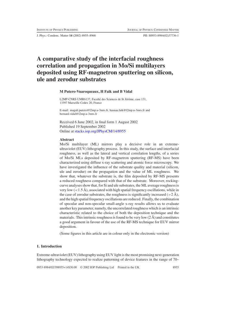
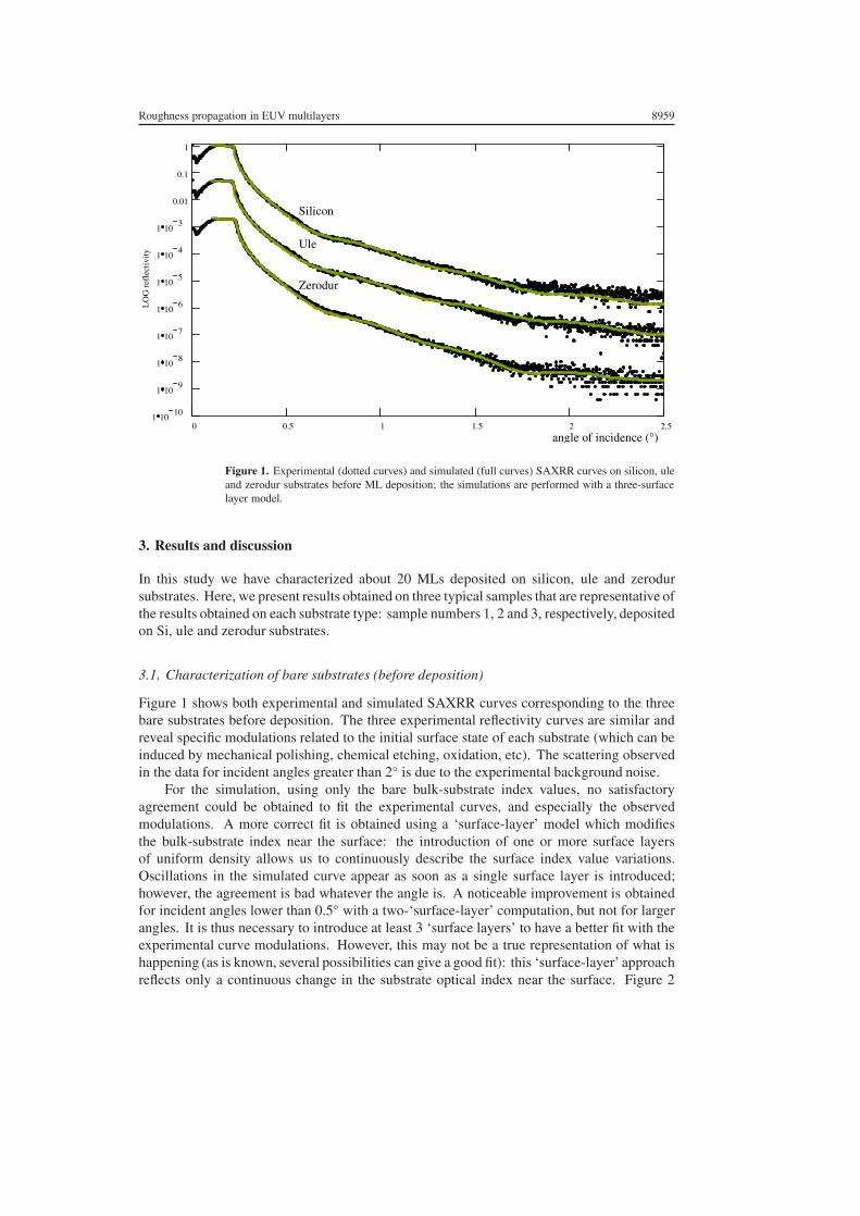
Figure 1. Experimental (dotted curves) and simulated (full curves) SAXRR curves on silicon, uleand zerodur substrates before ML deposition; the simulations are performed with a three-surfacelayer model.
3. Results and discussion
In this study we have characterized about 20 MLs deposited on silicon, ule and zerodursubstrates. Here, we present results obtained on three typical samples that are representative ofthe results obtained on each substrate type: sample numbers 1, 2 and 3, respectively, depositedon Si, ule and zerodur substrates.
3.1. Characterization of bare substrates (before deposition)
Figure 1 shows both experimental and simulated SAXRR curves corresponding to the threebare substrates before deposition. The three experimental reflectivity curves are similar andreveal specific modulations related to the initial surface state of each substrate (which can beinduced by mechanical polishing, chemical etching, oxidation, etc). The scattering observedin the data for incident angles greater than 2◦ is due to the experimental background noise.
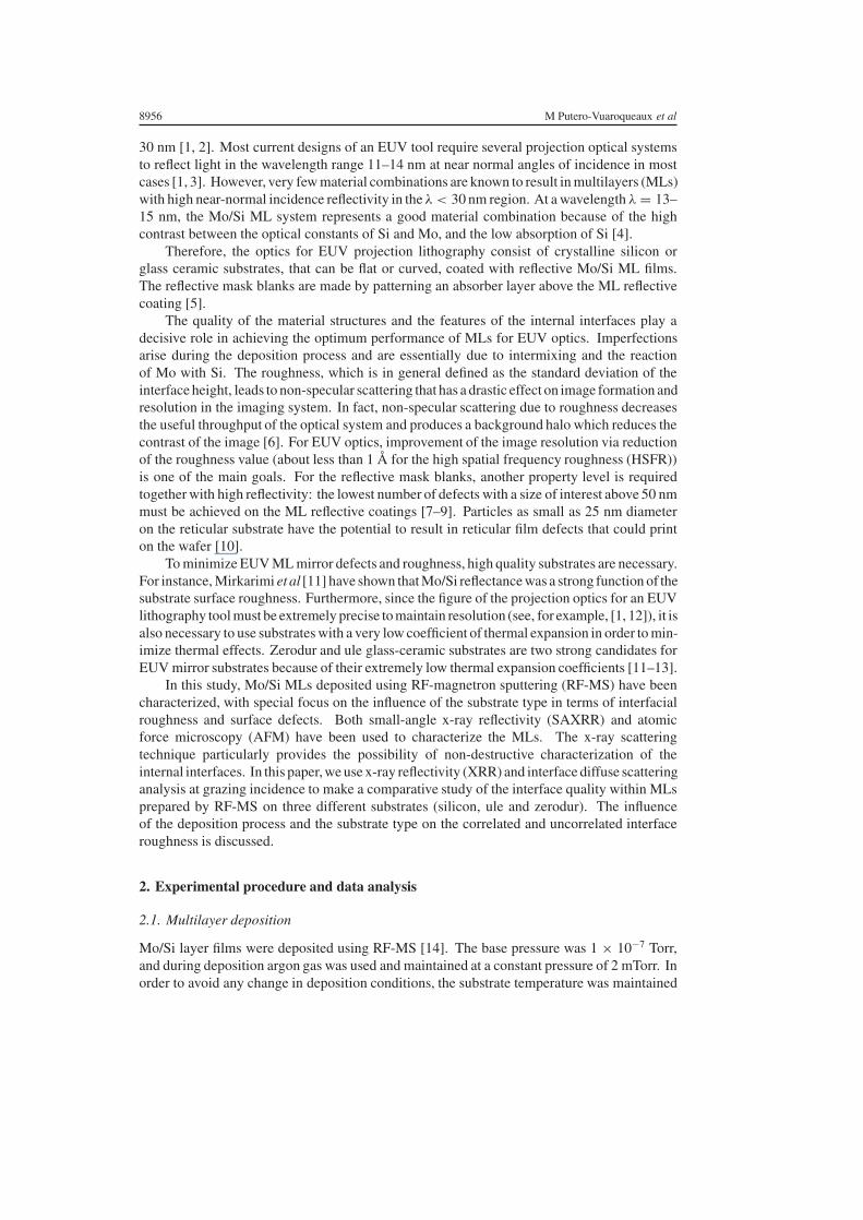
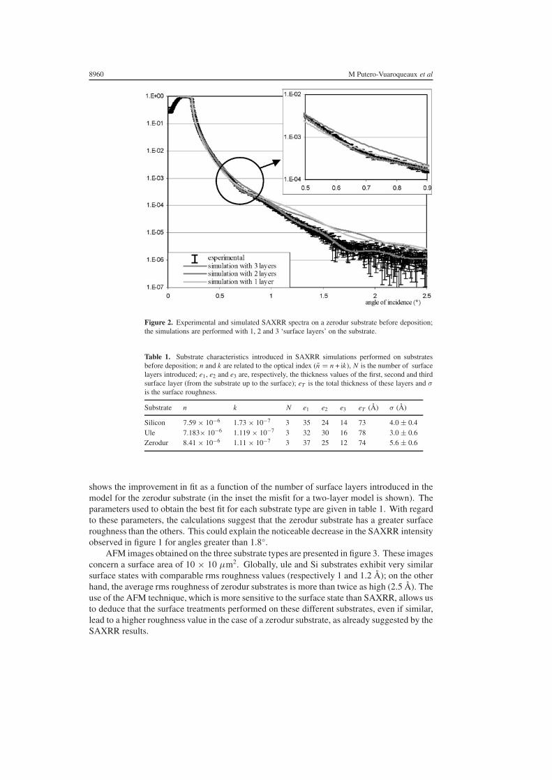
For the simulation, using only the bare bulk-substrate index values, no satisfactoryagreement could be obtained to fit the experimental curves, and especially the observedmodulations. A more correct fit is obtained using a ‘surface-layer’ model which modifiesthe bulk-substrate index near the surface: the introduction of one or more surface layersof uniform density allows us to continuously describe the surface index value variations.Oscillations in the simulated curve appear as soon as a single surface layer is introduced;however, the agreement is bad whatever the angle is. A noticeable improvement is obtainedfor incident angles lower than 0.5◦ with a two-‘surface-layer’ computation, but not for largerangles. It is thus necessary to introduce at least 3 ‘surface layers’ to have a better fit with theexperimental curve modulations. However, this may not be a true representation of what ishappening (as is known, several possibilities can give a good fit): this ‘surface-layer’ approachreflects only a continuous change in the substrate optical index near the surface. Figure 2
8960 M Putero-Vuaroqueaux et al
Figure 2. Experimental and simulated SAXRR spectra on a zerodur substrate before deposition;the simulations are performed with 1, 2 and 3 ‘surface layers’ on the substrate.
Table 1. Substrate characteristics introduced in SAXRR simulations performed on substratesbefore deposition; n and k are related to the optical index (n = n + ik), N is the number of surfacelayers introduced; e1, e2 and e3 are, respectively, the thickness values of the first, second and thirdsurface layer (from the substrate up to the surface); eT is the total thickness of these layers and σ
is the surface roughness.
Substrate n k N e1 e2 e3 eT (Å) σ (Å)
Silicon 7.59 × 10⁻⁶ 1.73 × 10⁻⁷ 3 35 24 14 73 4.0 ± 0.4Ule 7.183× 10⁻⁶ 1.119 × 10⁻⁷ 3 32 30 16 78 3.0 ± 0.6Zerodur 8.41 × 10⁻⁶ 1.11 × 10⁻⁷ 3 37 25 12 74 5.6 ± 0.6
shows the improvement in fit as a function of the number of surface layers introduced in themodel for the zerodur substrate (in the inset the misfit for a two-layer model is shown). Theparameters used to obtain the best fit for each substrate type are given in table 1. With regardto these parameters, the calculations suggest that the zerodur substrate has a greater surfaceroughness than the others. This could explain the noticeable decrease in the SAXRR intensityobserved in figure 1 for angles greater than 1.8◦.
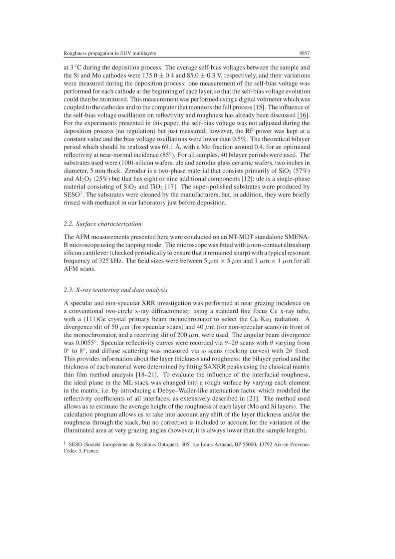
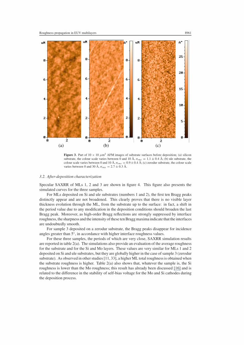
AFM images obtained on the three substrate types are presented in figure 3. These imagesconcern a surface area of 10 × 10 µm2. Globally, ule and Si substrates exhibit very similarsurface states with comparable rms roughness values (respectively 1 and 1.2 Å); on the otherhand, the average rms roughness of zerodur substrates is more than twice as high (2.5 Å). Theuse of the AFM technique, which is more sensitive to the surface state than SAXRR, allows usto deduce that the surface treatments performed on these different substrates, even if similar,lead to a higher roughness value in the case of a zerodur substrate, as already suggested by theSAXRR results.
Roughness propagation in EUV multilayers 8961
(a) (b) (c)
Figure 3. Part of 10 × 10 µm2 AFM images of substrate surfaces before deposition; (a) siliconsubstrate, the colour scale varies between 0 and 10 Å, σrms = 1.1 ± 0.4 Å; (b) ule substrate, thecolour scale varies between 0 and 10 Å, σrms = 0.9 ± 0.4 Å; (c) zerodur substrate, the colour scalevaries between 0 and 30 Å, σrms = 2.7 ± 0.3 Å.
3.2. After-deposition characterization
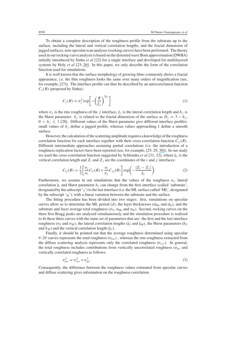
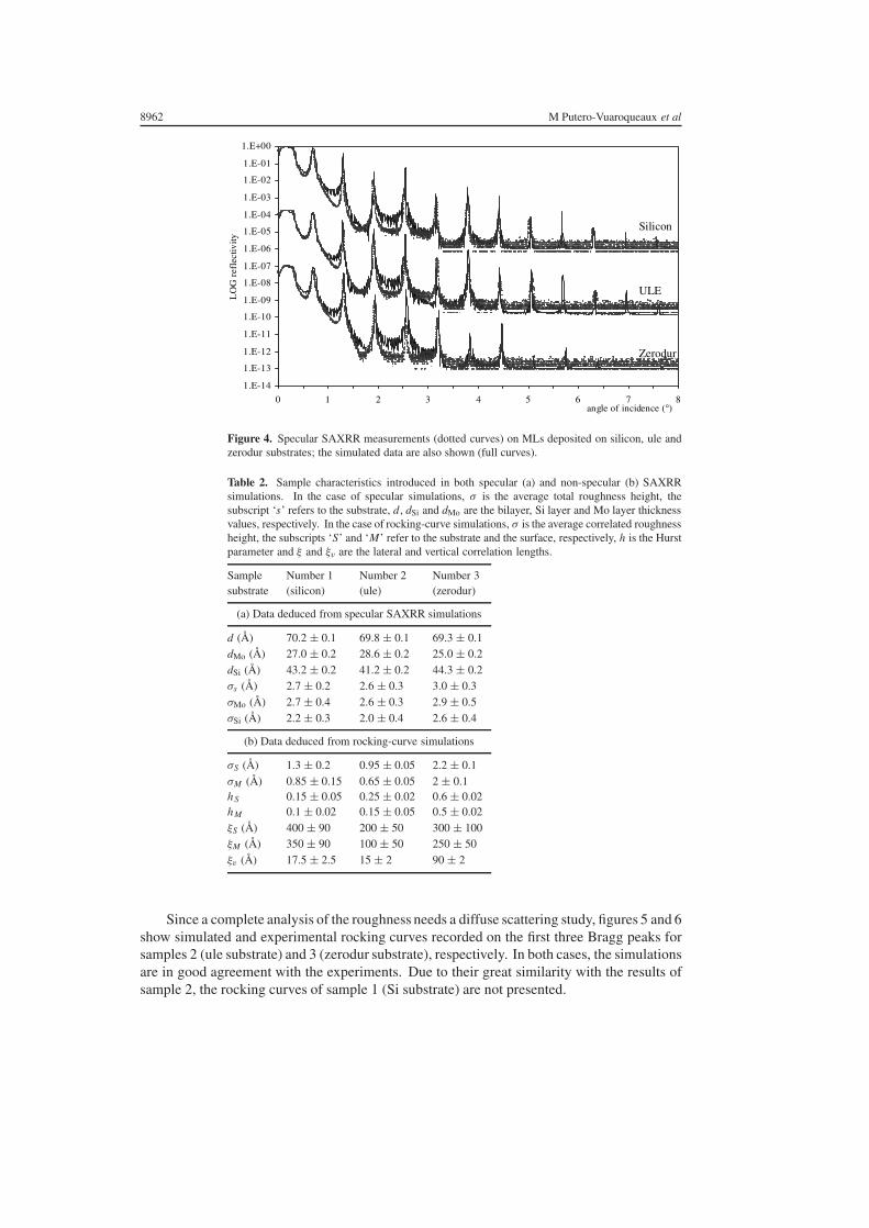
Specular SAXRR of MLs 1, 2 and 3 are shown in figure 4. This figure also presents thesimulated curves for the three samples.
For MLs deposited on Si and ule substrates (numbers 1 and 2), the first ten Bragg peaksdistinctly appear and are not broadened. This clearly proves that there is no visible layerthickness evolution through the ML, from the substrate up to the surface: in fact, a shift inthe period value due to any modification in the deposition conditions should broaden the lastBragg peak. Moreover, as high-order Bragg reflections are strongly suppressed by interfaceroughness, the sharpness and the intensity of these ten Bragg maxima indicate that the interfacesare undoubtedly smooth.
For sample 3 deposited on a zerodur substrate, the Bragg peaks disappear for incidenceangles greater than 5◦, in accordance with higher interface roughness values.
For these three samples, the periods of which are very close, SAXRR simulation resultsare reported in table 2(a). The simulations also provide an evaluation of the average roughnessfor the substrate and for the Si and Mo layers. These values are very similar for MLs 1 and 2deposited on Si and ule substrates, but they are globally higher in the case of sample 3 (zerodursubstrate). As observed in other studies [11, 33], a higher ML total roughness is obtained whenthe substrate roughness is higher. Table 2(a) also shows that, whatever the sample is, the Siroughness is lower than the Mo roughness; this result has already been discussed [16] and isrelated to the difference in the stability of self-bias voltage for the Mo and Si cathodes duringthe deposition process.
8962 M Putero-Vuaroqueaux et al
1.E-14
1.E-13
1.E-12
1.E-11
1.E-10
1.E-09
1.E-08
1.E-07
1.E-06
1.E-05
1.E-04
1.E-03
1.E-02
1.E-01
1.E+00
0 1 2 3 4 5 6 7 8angle of incidence (°)
LO
G r
efle
ctiv
itySilicon
ULE
Zerodur
Figure 4. Specular SAXRR measurements (dotted curves) on MLs deposited on silicon, ule andzerodur substrates; the simulated data are also shown (full curves).
Table 2. Sample characteristics introduced in both specular (a) and non-specular (b) SAXRRsimulations. In the case of specular simulations, σ is the average total roughness height, thesubscript ‘s’ refers to the substrate, d, dSi and dMo are the bilayer, Si layer and Mo layer thicknessvalues, respectively. In the case of rocking-curve simulations, σ is the average correlated roughnessheight, the subscripts ‘S’ and ‘M’ refer to the substrate and the surface, respectively, h is the Hurstparameter and ξ and ξv are the lateral and vertical correlation lengths.
Sample Number 1 Number 2 Number 3substrate (silicon) (ule) (zerodur)
(a) Data deduced from specular SAXRR simulations
d (Å) 70.2 ± 0.1 69.8 ± 0.1 69.3 ± 0.1dMo (Å) 27.0 ± 0.2 28.6 ± 0.2 25.0 ± 0.2dSi (Å) 43.2 ± 0.2 41.2 ± 0.2 44.3 ± 0.2σs (Å) 2.7 ± 0.2 2.6 ± 0.3 3.0 ± 0.3σMo (Å) 2.7 ± 0.4 2.6 ± 0.3 2.9 ± 0.5σSi (Å) 2.2 ± 0.3 2.0 ± 0.4 2.6 ± 0.4
(b) Data deduced from rocking-curve simulations
σS (Å) 1.3 ± 0.2 0.95 ± 0.05 2.2 ± 0.1σM (Å) 0.85 ± 0.15 0.65 ± 0.05 2 ± 0.1hS 0.15 ± 0.05 0.25 ± 0.02 0.6 ± 0.02hM 0.1 ± 0.02 0.15 ± 0.05 0.5 ± 0.02ξS (Å) 400 ± 90 200 ± 50 300 ± 100ξM (Å) 350 ± 90 100 ± 50 250 ± 50ξv (Å) 17.5 ± 2.5 15 ± 2 90 ± 2
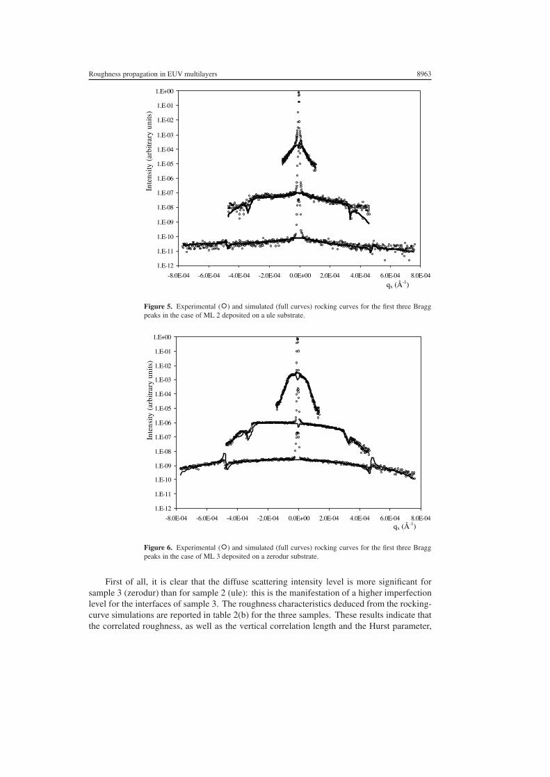
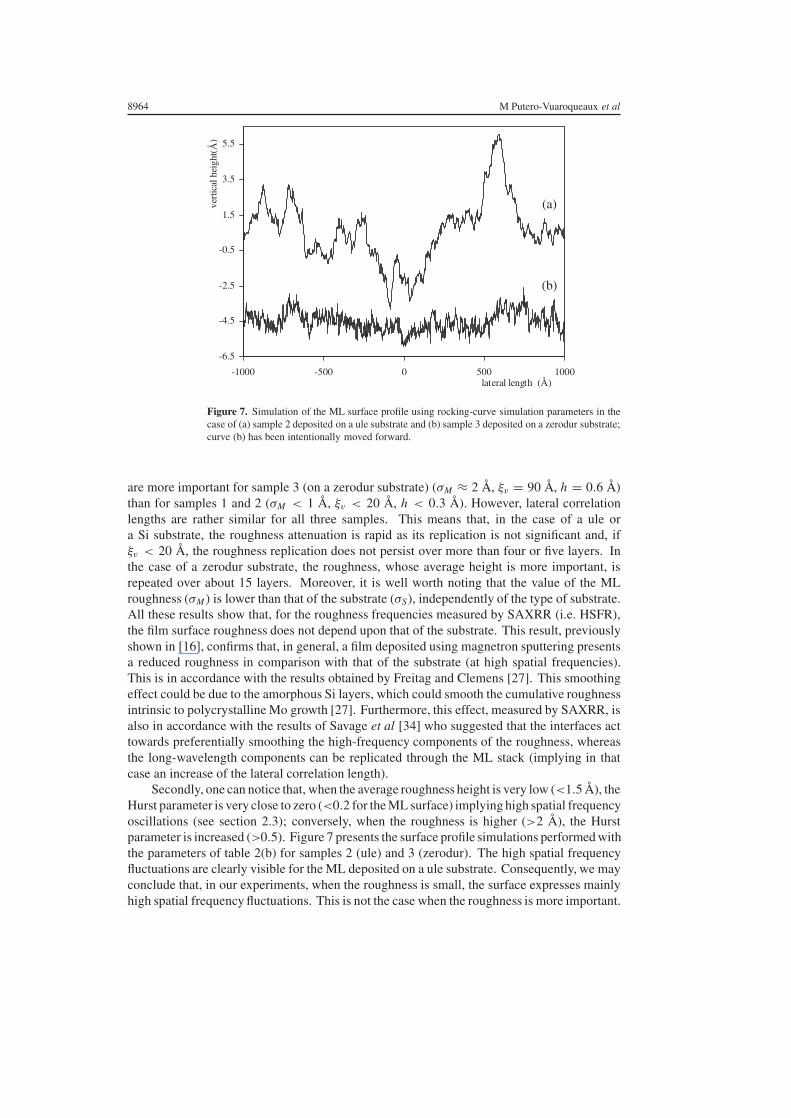
Since a complete analysis of the roughness needs a diffuse scattering study, figures 5 and 6show simulated and experimental rocking curves recorded on the first three Bragg peaks forsamples 2 (ule substrate) and 3 (zerodur substrate), respectively. In both cases, the simulationsare in good agreement with the experiments. Due to their great similarity with the results ofsample 2, the rocking curves of sample 1 (Si substrate) are not presented.
Roughness propagation in EUV multilayers 8963
1.E-12
1.E-11
1.E-10
1.E-09
1.E-08
1.E-07
1.E-06
1.E-05
1.E-04
1.E-03
1.E-02
1.E-01
1.E+00
-8.0E-04 -6.0E-04 -4.0E-04 -2.0E-04 0.0E+00 2.0E-04 4.0E-04 6.0E-04 8.0E-04
Inte
nsity
(ar
bitr
ary
units
)
qx (Å-1)
Figure 5. Experimental (◦) and simulated (full curves) rocking curves for the first three Braggpeaks in the case of ML 2 deposited on a ule substrate.
1.E-12
1.E-11
1.E-10
1.E-09
1.E-08
1.E-07
1.E-06
1.E-05
1.E-04
1.E-03
1.E-02
1.E-01
1.E+00
-8.0E-04 -6.0E-04 -4.0E-04 -2.0E-04 0.0E+00 2.0E-04 4.0E-04 6.0E-04 8.0E-04
Inte
nsity
(ar
bitr
ary
units
)
qx (Å-1)
Figure 6. Experimental (◦) and simulated (full curves) rocking curves for the first three Braggpeaks in the case of ML 3 deposited on a zerodur substrate.
First of all, it is clear that the diffuse scattering intensity level is more significant forsample 3 (zerodur) than for sample 2 (ule): this is the manifestation of a higher imperfectionlevel for the interfaces of sample 3. The roughness characteristics deduced from the rocking-curve simulations are reported in table 2(b) for the three samples. These results indicate thatthe correlated roughness, as well as the vertical correlation length and the Hurst parameter,
8964 M Putero-Vuaroqueaux et al
-6.5
-4.5
-2.5
-0.5
1.5
3.5
5.5
-1000 -500 0 500 1000lateral length (Å)
vert
ical
hei
ght(
Å)
(b)
(a)
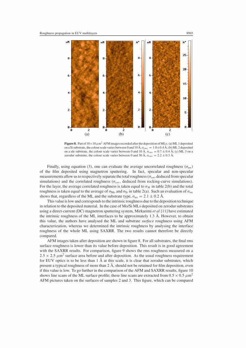
Figure 7. Simulation of the ML surface profile using rocking-curve simulation parameters in thecase of (a) sample 2 deposited on a ule substrate and (b) sample 3 deposited on a zerodur substrate;curve (b) has been intentionally moved forward.
are more important for sample 3 (on a zerodur substrate) (σM ≈ 2 Å, ξv = 90 Å, h = 0.6 Å)than for samples 1 and 2 (σM < 1 Å, ξv < 20 Å, h < 0.3 Å). However, lateral correlationlengths are rather similar for all three samples. This means that, in the case of a ule ora Si substrate, the roughness attenuation is rapid as its replication is not significant and, ifξv < 20 Å, the roughness replication does not persist over more than four or five layers. Inthe case of a zerodur substrate, the roughness, whose average height is more important, isrepeated over about 15 layers. Moreover, it is well worth noting that the value of the MLroughness (σM ) is lower than that of the substrate (σS), independently of the type of substrate.All these results show that, for the roughness frequencies measured by SAXRR (i.e. HSFR),the film surface roughness does not depend upon that of the substrate. This result, previouslyshown in [16], confirms that, in general, a film deposited using magnetron sputtering presentsa reduced roughness in comparison with that of the substrate (at high spatial frequencies).This is in accordance with the results obtained by Freitag and Clemens [27]. This smoothingeffect could be due to the amorphous Si layers, which could smooth the cumulative roughnessintrinsic to polycrystalline Mo growth [27]. Furthermore, this effect, measured by SAXRR, isalso in accordance with the results of Savage et al [34] who suggested that the interfaces acttowards preferentially smoothing the high-frequency components of the roughness, whereasthe long-wavelength components can be replicated through the ML stack (implying in thatcase an increase of the lateral correlation length).
Secondly, one can notice that, when the average roughness height is very low (<1.5 Å), theHurst parameter is very close to zero (<0.2 for the ML surface) implying high spatial frequencyoscillations (see section 2.3); conversely, when the roughness is higher (>2 Å), the Hurstparameter is increased (>0.5). Figure 7 presents the surface profile simulations performed withthe parameters of table 2(b) for samples 2 (ule) and 3 (zerodur). The high spatial frequencyfluctuations are clearly visible for the ML deposited on a ule substrate. Consequently, we mayconclude that, in our experiments, when the roughness is small, the surface expresses mainlyhigh spatial frequency fluctuations. This is not the case when the roughness is more important.
Roughness propagation in EUV multilayers 8965
(a) (b) (c)
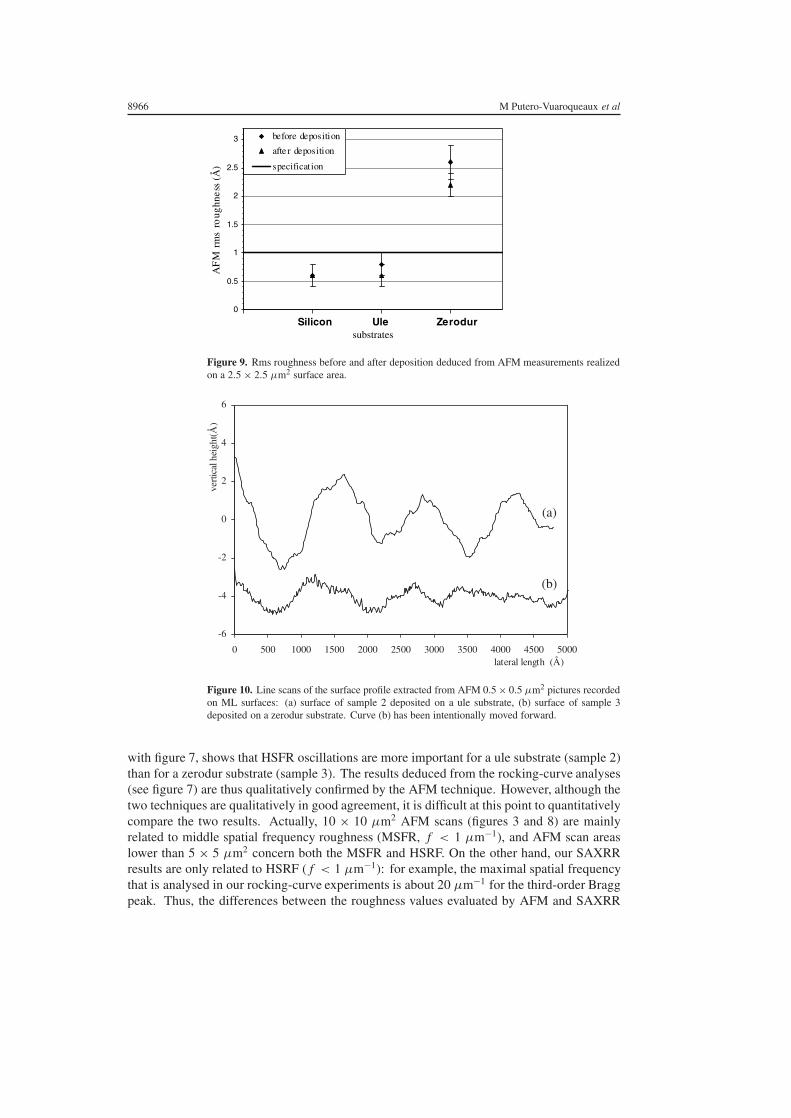
Figure 8. Part of 10×10 µm2 AFM images recorded after the deposition of MLs; (a) ML 1 depositedon a Si substrate, the colour scale varies between 0 and 10 Å, σrms = 1.0±0.4 Å; (b) ML 2 depositedon a ule substrate, the colour scale varies between 0 and 10 Å, σrms = 0.7 ± 0.4 Å; (c) ML 3 on azerodur substrate, the colour scale varies between 0 and 30 Å, σrms = 2.2 ± 0.3 Å.
Finally, using equation (3), one can evaluate the average uncorrelated roughness (σun)
of the film deposited using magnetron sputtering. In fact, specular and non-specularmeasurements allow us to respectively separate the total roughness (σtot, deduced from specularsimulations) and the correlated roughness (σcor , deduced from rocking-curve simulations).For the layer, the average correlated roughness is taken equal to σM in table 2(b) and the totalroughness is taken equal to the average of σMo and σSi in table 2(a). Such an evaluation of σun
shows that, regardless of the ML and the substrate type, σun = 2.1 ± 0.2 Å.This value is low and corresponds to the intrinsic roughness due to the deposition technique
in relation to the deposited material. In the case of Mo/Si MLs deposited on zerodur substratesusing a direct-current (DC) magnetron sputtering system, Mirkarimi et al [11] have estimatedthe intrinsic roughness of the ML interfaces to be approximately 1.3 Å. However, to obtainthis value, the authors have analysed the ML and substrate surface roughness using AFMcharacterization, whereas we determined the intrinsic roughness by analysing the interfaceroughness of the whole ML using SAXRR. The two results cannot therefore be directlycompared.
AFM images taken after deposition are shown in figure 8. For all substrates, the final rmssurface roughness is lower than its value before deposition. This result is in good agreementwith the SAXRR results. For comparison, figure 9 shows the rms roughness measured on a2.5 × 2.5 µm2 surface area before and after deposition. As the usual roughness requirementfor EUV optics is to be less than 1 Å at this scale, it is clear that zerodur substrates, whichpresent a typical roughness of more than 2 Å, should not be retained for film deposition, evenif this value is low. To go further in the comparison of the AFM and SAXRR results, figure 10shows line scans of the ML surface profile; these line scans are extracted from 0.5 × 0.5 µm2
AFM pictures taken on the surfaces of samples 2 and 3. This figure, which can be compared
8966 M Putero-Vuaroqueaux et al
0
0.5
1
1.5
2
2.5
3
4 6
AF
M r
ms
roug
hnes
s (Å
)
before deposition
afte r deposition
specification
Ule ZerodurSiliconsubstrates
Figure 9. Rms roughness before and after deposition deduced from AFM measurements realizedon a 2.5 × 2.5 µm2 surface area.
-6
-4
-2
0
2
4
6
0 500 1000 1500 2000 2500 3000 3500 4000 4500 5000lateral length (Å)
verti
cal h
eigh
t(Å
)
(b)
(a)
Figure 10. Line scans of the surface profile extracted from AFM 0.5 × 0.5 µm2 pictures recordedon ML surfaces: (a) surface of sample 2 deposited on a ule substrate, (b) surface of sample 3deposited on a zerodur substrate. Curve (b) has been intentionally moved forward.
with figure 7, shows that HSFR oscillations are more important for a ule substrate (sample 2)than for a zerodur substrate (sample 3). The results deduced from the rocking-curve analyses(see figure 7) are thus qualitatively confirmed by the AFM technique. However, although thetwo techniques are qualitatively in good agreement, it is difficult at this point to quantitativelycompare the two results. Actually, 10 × 10 µm2 AFM scans (figures 3 and 8) are mainlyrelated to middle spatial frequency roughness (MSFR, f < 1 µm−1), and AFM scan areaslower than 5 × 5 µm2 concern both the MSFR and HSRF. On the other hand, our SAXRRresults are only related to HSRF ( f < 1 µm−1): for example, the maximal spatial frequencythat is analysed in our rocking-curve experiments is about 20 µm−1 for the third-order Braggpeak. Thus, the differences between the roughness values evaluated by AFM and SAXRR
Roughness propagation in EUV multilayers 8967
could also be explained by the differences between the spatial frequency ranges of the twotechniques. Thus, in order to perform a quantitative comparison of both roughness results, itis necessary to evaluate the rms roughness according to the spatial frequency (with the powerspectral density analysis).
For technical applications, the results concerning Si and ule substrates renders them moreadvantageous for the EUV mirror deposition. However, considering the conditions of use, ulesubstrates would be preferable owing to their low thermal expansion value.
4. Conclusion
We have studied the influence of the substrate quality and the deposition technique on thepropagation and value of the ML roughness, by combining specular and non-specular SAXRRand AFM techniques. The results show that, whatever the substrate roughness is, the depositionprocess smooths the film, so that the final roughness is always lower than the initial one.Moreover, the rocking-curve simulation data give us access to important parameters such asthe vertical correlation length, the Hurst parameter and the average correlated roughness of thesubstrate and the ML surface. These results show that, for Si and ule substrates, the averageroughness height is very low (σ < 1.5 Å), associated with high-spatial-frequency oscillations(h < 0.2), whereas in the case of a zerodur substrate, the roughness value is significantlyincreased (σ > 2 Å), and the high-spatial-frequency oscillations are reduced (h > 0.6). Theseparameters concern, in fact, each interface in the ML and are thus important for the EUVoptics. Although the real influence of such fluctuations on EUV imaging processes is notquite clear at present, it seems preferable to have an average roughness lower than 2 Å as thetechnical requirements always impose the lowest roughness values. In these conditions, andtaking into account our results, Si and ule substrates can be considered as the best candidatesfor EUV optics, as compared with zerodur substrates. However, it is important to note that theSi thermal expansion coefficient is not small enough to prevent harmful thermal effects.
The combination of specular and non-specular SAXRR results leads to the evaluation ofanother key parameter, the uncorrelated roughness, which is an intrinsic characteristic relatedto both the chosen deposition technique and the material. In our case, using RF-magnetronsputtering and Si and Mo materials, we find a characteristic intrinsic roughness of 2 Å. Thisvalue is very low and constitutes a good argument in favour of the use of this technique forEUV mirror deposition.
The roughness values evaluated by SAXRR and AFM are similar. However, for furtherstudy of the correlation between the roughness values evaluated by these techniques, one needsto use the power spectral density analysis in order to correctly compare the rms roughness valuewith that of the spatial frequency roughness. This work is in progress.
References
[1] Gwyn C W, Stulen R H, Sweeney D W and Attwood D 1998 EUV lithography J. Vac. Sci. Technol. B 16 3142–9[2] Taylor J S, Sommargren G E, Sweeney D W and Hudyma R M 1998 Proc. SPIE–Int. Soc. Opt. Eng. 3331
580–90[3] Sweeney D W, Chapman H N, Hudyma R M and Shafer D R 1998 EUV optical design for a 100 nm CD imaging
system Emerging Lithographic Technologies II (Proc. SPIE vol 3331) ed Y Vladirmirsky pp 2–10[4] Stearns D G, Rosen R S and Vernon P 1991 J. Vac. Sci. Technol. A 9 2662[5] Tenant D M, Bjorkholm J E, D’Souza R, Eichner L, Freeman R R, Pastalan J Z, Szeto L H, Wood O R II,
Jewell T E, Mansfield W M, Waskiewics W K, White D L, Windt D L and MacDowell A A 1991 J. Vac. Sci.Technol. B 9 3176
[6] Stearns D G, Gaines D P and Sweeney D W 1998 J. Appl. Phys. 84 1003–28
8968 M Putero-Vuaroqueaux et al
[7] Nguyen K B and Nguyen T D 1993 J. Vac. Sci. Technol. B 11 2960–2970[8] Hue J, Muffato V, Pelle C, Quesnel E, Garrec P and Baume F 2001 Proc. SPIE–Int. Soc. Opt. Eng. 4343 627–38[9] Burkhart S, Cerjan C, Kearney P, Mirkarimi P and Walton C 1999 Low-defect reflective mask blanks for extreme
ultraviolet lithography Part of the SPIE Conf. on Emerging Lithographic Technologies III vol 3676 pp 570–7[10] Pistor T, Deng Y F and Neureuther A 2000 Extreme ultraviolet mask defect simulation: low-profile defects
J. Vac. Sci. Technol. B 18 2926–9[11] Mirkarimi P B, Bajt S and Wall M A 2000 Appl. Opt. 39 1617–25[12] Bach H 1995 Low Expansion Glass Ceramics (Heidelberg: Springer)[13] Mirkarimi P B, Baker S L, Montcalm C and Folta J A 2001 Appl. Opt. 40 62–70[14] Vidal B and Marfaing J 1991 Opt. Eng. 30 636[15] Cilia M, Yakschin A, Trambly H, Vidal B and Bretagne J 1998 Thin Solid Films 312 320–6[16] Putero-Vuaroqueaux M and Vidal B 2001 Extreme ultraviolet multilayer mirrors deposited using radio-
frequency-magnetron sputtering: the influence of self bias voltage on reflectivity and roughness J. Phys.:Condens. Matter 13 3969–76
[17] Gulati S T 1992 Mechanical properties of SiO2 vs SiO2–TiO2 bulk glasses and fibers Optical WaveguideMaterials vol 244, ed M M Broer, G H Siegel, R T Kersten and H Kawazoe (Pittsburgh, PA: MaterialsResearch Society) pp 67–84
[18] Parrat L G 1954 Phys. Rev. 95 359[19] Nevot Louis 1978 PhD Thesis Universite de Paris-Sud, Centre Orsay[20] Lee P 1981 Opt. Commun. 37 159[21] Vidal B and Vincent P 1984 Appl. Opt. 23 1794[22] Sinha S K, Sirota E B, Garoff S and Stanley H B 1988 Phys. Rev. B 38 2297[23] Holy V, Kubena J, Ohlidal I, Lisckla K and Plotz W 1993 Phys. Rev. B 47 15 896[24] Wong P Z and Bray A 1989 Phys. Rev. B 37 7751[25] Holy V and Baumbach T 1994 Phys. Rev. B 49 10 668[26] Holy V, Pietsch U and Baumbach T 1998 X-ray Scattering by Thin Films and Multilayers (Berlin: Springer)[27] Freitag J M and Clemens B M 2001 J. Appl. Phys. 89 1101–7[28] Mandelbrodt B B 1982 The Fractal Geometry of Nature (New York: Freeman)[29] Kaganer V M, Stepanov S A and Kolher R 1996 Physica B 221 34[30] Ming Z H, Krol A, Soo Y L, Kao Y H, Park J S and Wang K L 1993 Phys. Rev. B 47 16 373[31] Trambly de Laissardiere H 1997 Etude de miroirs multicouches X en reflexion et lumiere diffuse. Application
a l’analyse des multicouches implantees et a la fabrication d’optique diffractive PhD Thesis University ofAix-Marseille III
[32] Schlomka J P, Fitzsimmons M R, Pynn R, Stettner J, Seeck O H, Tolan M and Press W 1996 Physica B 221 44[33] Ulyanenkov A, Matsuo R, Omote K, Inaba K, Harada J, Ishino M, Nishii M and Yoda O 2000 J. Appl. Phys. 87
7255–60[34] Savage D E, Shimke N, Phang Y H and Lagally M G 1992 J. Appl. Phys. 71 3283
Related Documents


