A compact quantum model of nanoscale double-gate metal-oxide-semiconductor field-effect transistor for high frequency and noise simulations A. Lázaro, a B. Nae, O. Moldovan, and B. Iñiguez Departament d’Enginyeria Electrónica, Eléctrica i Automática, Universitat Rovira i Virgili, 43007 Tarragona, Spain Received 19 June 2006; accepted 21 July 2006; published online 26 October 2006 In this paper, we present an analytical model for high frequency and microwave noise model of nanoscale double-gate metal-oxide-semiconductor field-effect transistor. The model is based on a compact model for charge quantization within the channel and it includes overshoot velocity effects. Radio-frequency and noise performances are calculated using an active transmission line method. A comparison is made between classical and quantum charge control and between drift diffusion and hydrodynamic models. © 2006 American Institute of Physics. DOI: 10.1063/1.2360379 I. INTRODUCTION Ultrathin-film body metal-oxide-semiconductor MOS transistors, and in particular, double-gate DG metal-oxide- semiconductor field-effect transistors MOSFETs, are con- sidered to be a very attractive option to improve the perfor- mance of complementary metal-oxide-semiconductor CMOS devices and overcome some of the difficulties en- countered in further downscaling of MOS field-effect tran- sistors into the sub-50 nm gate length regime. 1–5 One of the limiting factors in MOSFET downscaling is the static power consumption due to short channel effects SCEs, including threshold voltage roll-off and subthreshold slope degrada- tion. These effects increase the off-state leakage current. In DG-MOSFETs, the control of the channel by the gate is stronger than in planar single-gate MOSFETs. Drain-induced barrier-height lowering DIBL, threshold voltage roll-off, and off-state leakage can be significantly reduced. 1–5 Be- cause of such advantages, these devices will be preferred in nanoscale circuits, thus making the development of computer-aided-design CAD compatible models a matter of urgency. Nanoscale DG-MOSFETs introduce challenges to com- pact modeling associated with the enhanced coupling be- tween the electrodes source drain and gates, quantum con- finement, ballistic or quasiballistic transport, gate tunneling current, etc. Most models presented so far are for undoped devices with a long enough channel to assume that the trans- port is due to the drift-diffusion mechanism. 5–8 Very little work has been done on the transition from the ballistic re- gime to drift diffusion. 9–11 Regarding modeling of the elec- trostatics, most of the work has been based on solving the one-dimensional 1D Poisson equation perpendicular to the gates, thereby neglecting short-channel effects. As a result of the downscaling of MOSFETs into the sub-0.1-m regime, the high frequency capabilities of the transistor have reached well into the gigahertz range, creat- ing opportunities for rf circuit applications and opening mar- kets in the microwave and millimeter wave regions. Over the last years, the growing interest in bulk and silicon-on- insulator SOI MOSFETs for the microwave domain is evi- denced by an increased activity in the relevant literature. 12,13 High-resistivity SOI substrates have demonstrated a higher superiority over standard-resistivity SOI and bulk silicon with regard to cross talk at frequencies up to 10 GHz. 14 Also SOI technologies are preferred for rf applications due to their lower losses in passive devices. However, little work has been done on the development of high frequency nanoscale DG-MOSFET compact models. Due to scaling, the silicon thickness is ultrathin and quantum confinement must be included in the models. Then, a self-consistent solution of Schrödinger-Poisson equations is needed. Numerical solutions are described in the literature for these transistors, 15,16 but analytical models are preferred for compact models that can be easily incorporated in com- mercial CAD software. 17 The self-consistency between Pois- son’s and Schrödinger’s equations is one of the main model- ing challenges in nanoscale devices, but most of the published models ignore it. 17–21 Our starting point is a classical model without quantifi- cation effects for the doped double-gate MOSFET, which is analytical, explicit, and continuous. It is based on a previous work, 7 which presented a current model valid for low V ds . Our model works in all operating regimes from weak to strong inversion and from linear regime to saturation. The current expression is based on a unified charge control model, written in terms of charge densities at the source and drain ends, 22,23 and derived for a doped DG-MOSFET. We use an accurate explicit expression of the inversion charge densities in terms of the applied bias. The model is continu- ous through all operation regimes linear, saturation, and subthreshold. No fitting parameters are used in the charge control model. The model is valid up to well above thresh- old. Actually these devices are not operated at high values of V gs , and therefore the model is valid for the regimes of prac- tical interest. This classical unified charge control model is extended to include quantification effects within the channel. This ex- a Electronic mail: [email protected] JOURNAL OF APPLIED PHYSICS 100, 084320 2006 0021-8979/2006/1008/084320/12/$23.00 © 2006 American Institute of Physics 100, 084320-1 Downloaded 26 Dec 2006 to 140.120.11.249. Redistribution subject to AIP license or copyright, see http://jap.aip.org/jap/copyright.jsp

Welcome message from author
This document is posted to help you gain knowledge. Please leave a comment to let me know what you think about it! Share it to your friends and learn new things together.
Transcript
A compact quantum model of nanoscale double-gatemetal-oxide-semiconductor field-effect transistor for highfrequency and noise simulations
A. Lázaro,a� B. Nae, O. Moldovan, and B. IñiguezDepartament d’Enginyeria Electrónica, Eléctrica i Automática, Universitat Rovira i Virgili,43007 Tarragona, Spain
�Received 19 June 2006; accepted 21 July 2006; published online 26 October 2006�
In this paper, we present an analytical model for high frequency and microwave noise model ofnanoscale double-gate metal-oxide-semiconductor field-effect transistor. The model is based on acompact model for charge quantization within the channel and it includes overshoot velocity effects.Radio-frequency and noise performances are calculated using an active transmission line method. Acomparison is made between classical and quantum charge control and between drift diffusion andhydrodynamic models. © 2006 American Institute of Physics. �DOI: 10.1063/1.2360379�
I. INTRODUCTION
Ultrathin-film body metal-oxide-semiconductor �MOS�transistors, and in particular, double-gate �DG� metal-oxide-semiconductor field-effect transistors �MOSFETs�, are con-sidered to be a very attractive option to improve the perfor-mance of complementary metal-oxide-semiconductor�CMOS� devices and overcome some of the difficulties en-countered in further downscaling of MOS field-effect tran-sistors into the sub-50 nm gate length regime.1–5 One of thelimiting factors in MOSFET downscaling is the static powerconsumption due to short channel effects �SCEs�, includingthreshold voltage roll-off and subthreshold slope degrada-tion. These effects increase the off-state leakage current. InDG-MOSFETs, the control of the channel by the gate isstronger than in planar single-gate MOSFETs. Drain-inducedbarrier-height lowering �DIBL�, threshold voltage roll-off,and off-state leakage can be significantly reduced.1–5 Be-cause of such advantages, these devices will be preferred innanoscale circuits, thus making the development ofcomputer-aided-design �CAD� compatible models a matterof urgency.
Nanoscale DG-MOSFETs introduce challenges to com-pact modeling associated with the enhanced coupling be-tween the electrodes �source drain and gates�, quantum con-finement, ballistic or quasiballistic transport, gate tunnelingcurrent, etc. Most models presented so far are for undopeddevices with a long enough channel to assume that the trans-port is due to the drift-diffusion mechanism.5–8 Very littlework has been done on the transition from the ballistic re-gime to drift diffusion.9–11 Regarding modeling of the elec-trostatics, most of the work has been based on solving theone-dimensional �1D� Poisson equation perpendicular to thegates, thereby neglecting short-channel effects.
As a result of the downscaling of MOSFETs into thesub-0.1-�m regime, the high frequency capabilities of thetransistor have reached well into the gigahertz range, creat-ing opportunities for rf circuit applications and opening mar-
kets in the microwave and millimeter wave regions. Over thelast years, the growing interest in bulk and silicon-on-insulator �SOI� MOSFETs for the microwave domain is evi-denced by an increased activity in the relevant literature.12,13
High-resistivity SOI substrates have demonstrated a highersuperiority over standard-resistivity SOI and bulk siliconwith regard to cross talk at frequencies up to 10 GHz.14 AlsoSOI technologies are preferred for rf applications due to theirlower losses in passive devices. However, little work hasbeen done on the development of high frequency nanoscaleDG-MOSFET compact models.
Due to scaling, the silicon thickness is ultrathin andquantum confinement must be included in the models. Then,a self-consistent solution of Schrödinger-Poisson equations isneeded. Numerical solutions are described in the literaturefor these transistors,15,16 but analytical models are preferredfor compact models that can be easily incorporated in com-mercial CAD software.17 The self-consistency between Pois-son’s and Schrödinger’s equations is one of the main model-ing challenges in nanoscale devices, but most of thepublished models ignore it.17–21
Our starting point is a classical model �without quantifi-cation effects� for the doped double-gate MOSFET, which isanalytical, explicit, and continuous. It is based on a previouswork,7 which presented a current model valid for low Vds.Our model works in all operating regimes from weak tostrong inversion and from linear regime to saturation. Thecurrent expression is based on a unified charge controlmodel, written in terms of charge densities at the source anddrain ends,22,23 and derived for a doped DG-MOSFET. Weuse an accurate explicit expression of the inversion chargedensities in terms of the applied bias. The model is continu-ous through all operation regimes �linear, saturation, andsubthreshold�. No fitting parameters are used in the chargecontrol model. The model is valid up to well above thresh-old. Actually these devices are not operated at high values ofVgs, and therefore the model is valid for the regimes of prac-tical interest.
This classical unified charge control model is extendedto include quantification effects within the channel. This ex-a�Electronic mail: [email protected]
JOURNAL OF APPLIED PHYSICS 100, 084320 �2006�
0021-8979/2006/100�8�/084320/12/$23.00 © 2006 American Institute of Physics100, 084320-1
Downloaded 26 Dec 2006 to 140.120.11.249. Redistribution subject to AIP license or copyright, see http://jap.aip.org/jap/copyright.jsp
tension is based on the analytical solution for Schrödinger’sequation for an infinite potential well.17 This hypothesis failsfor strong inversion region where the wave functions differfrom the case of infinite potential well.19,20 Using the conceptof inversion layer centroid,18,20 we introduce a correction inthe oxide capacitance in order to improve the accuracy in thestrong inversion bias region. Finally, we obtain a compactcharge control model including quantum effects whose ex-plicit formulation is similar to classical charge control. Ve-locity overshoot is included in the model using a one-dimensional energy-balance model.17 In contrast with themodel presented in Ref. 17 we include the effect of satura-tion region and the channel modulation length effect. Thelow-field mobility data use a model that takes into accountthe mobility degradation due to quantum effects.21
The dc model is extended to rf/microwave frequencyrange using the active transmission line approach.24–30 Dif-fusion and shot noise sources are included in the active linein order to study noise behavior of these transistors. Needlessto say, carrier temperature has a great influence in high fre-quency noise behavior. Whereas in the drift-diffusion modelsthe carrier temperature is considered using empirical rela-tionships with electric field, in the model presented here, thecarrier temperature along the channel is obtained from theenergy-balance model. In contrast with previous models forDG-MOSFETs,24–30 this paper presents a compact model forrf/noise applications including quantum effects and hydrody-namic transport. A comparison between drift-diffusion modeland nonstationary model will be presented.
II. dc MODEL
A. A classical charge control model
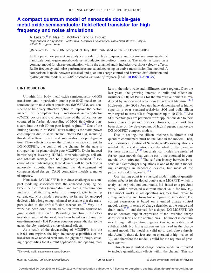
Figure 1 shows a scheme for a symmetrical DG-MOSFET. By using the gradual channel approximation, andneglecting the hole concentration, Poisson’s equation in ann-channel DG-MOSFET reads as
d2��x,y�dy2 =
q
�Si�NA +
ni2
NAe�q/kT����x,y�−V�x��� . �1�
The y axis is perpendicular to the surface and the x axisstarts at the source and ends at the drain region �see Fig. 1�.NA represents the doping density and ni is the intrinsic carrierconcentration. The potential is referred to as the neutral re-gion of one equivalent bulk MOS transistor. V�x� is the elec-tron quasi-Fermi potential depending on the voltage appliedto the channel between source and drain and is assumed to beindependent of x.7
The surface electric field can be written in terms of themobile charge density �in absolute value� per unit area Q andthe depletion charge density per unit area �in absolute value�Qdep=qNAtSi �tSi being the silicon film thickness�:
ES�x� =Q + Qdep
2�Si. �2�
By integrating �1� between the center and the surface of thefilm, we get
ES�x� =�2qNA
�Si���S − �0� +
kT
q
ni2
NA2 e�q/kT���S−V�y���1 − e−�q/kT���S−�0�� , �3�
where �S=��x ,−tSi /2� is the surface potential and �0
=��x ,0� is the potential in the middle of the film. Equation�3� cannot be analytically integrated for the potential, but it isobserved, from numerical simulations, that the difference�S−�0 keeps a constant value from the subthreshold regionto well above threshold.
At this point it is useful to define the average penetrationof the inversion-charge distribution yI into the silicon. Fol-lowing Ref. 18 due to the symmetry of the inversion-chargedistribution in symmetrical DG-MOSFET, we define yI byintegrating only half of the silicon film:
yI =
�0
tSi/2
yn�y�dy
�0
tSi/2
n�y�dy
=2q
Q�
0
tSi/2
yn�y�dy . �4�
Integrating the one-dimensional Poisson equation betweeny=0 and y= tSi /2 �neglecting majority-carrier concentrationand NA is assumed constant� results in the following expres-sion for the difference �S−�0:
FIG. 1. Double-gate MOSFET structure.
084320-2 Lázaro et al. J. Appl. Phys. 100, 084320 �2006�
Downloaded 26 Dec 2006 to 140.120.11.249. Redistribution subject to AIP license or copyright, see http://jap.aip.org/jap/copyright.jsp
�S − �0 =yI
2�SiQ +
qNAtSi2
8�Si=
yI
2�SiQ +
Qdep
8CSi. �5�
Note that, for weak inversion, the term yIQ� �Qdep/8CSi in�5� may be simplified to
�S − �0 qNAtSi
2
8�Si=
Qdep
8CSi, �6�
where CSi=�Si / tSi represents the silicon film capacitance.Approximation �6� is valid from subthreshold to well abovethreshold, which is demonstrated by the correct agreementwith simulations, for low and moderate Vgs�2 V�. For highVgs the surface potential increases much more rapidly thanthe midfilm potential, making the approximation less correct.
Equating �2� and �3� we obtain the following charge con-trol model:
Vgs − VFB − V − � Qdep
2Cox+
kT
qlog� q2
kT
NA3
ni2
tSi2
2�Si��
=Q
Cox+
kT
qlog� Q
Qdep� +
kT
qlog�Q + Qdep
Qdep� . �7�
Note that V varies from source to drain, being V=0 at thesource and V=Vds at the drain.12 VFB is the flatband voltageand Cox represents the capacitance of the oxide �Cox
=�ox/ tox�.In order to calculate the charge densities from an explicit
expression of the applied bias, we use the following equa-tion:
Q = 2Cox�−2Cox�
2
Qdep
+��2Cox�2
Qdep�2
+ 4�2 log2�1 + e�Vgs−Vth+�Vth−V�/2��� .
�8�
This expression �8� is similar to the expression used in sur-rounding gate MOSFETs,22,23 where the charge controlmodel has the same form as �6�. This expression tends to thedesired limits below and above threshold �see Ref. 23 fordetails�.
In �8� �=kT /q and Vth is defined as
Vth = V0 + 2� log�1 +Q�
2Qdep� . �9�
Q� is actually an initial iteration for Q:
Q� = 2Cox�−2Cox�
2
Qdep
+��2Cox�2
Qdep�2
+ 4�2 log2�1 + e�Vgs−V0−V�/2����10�
and
V0 = VFB + � Qdep
2Cox+
kT
qlog� q2
kT
NA3
ni2
tSi2
2�Si�� . �11�
The term �Vth ensures the correct behavior of Q abovethreshold:
�Vth =�Cox�
2/Qdep�Q�
Qdep + Q�/2. �12�
B. Quantum charge control model
Due to the confinement of electron motion normal to theSi–SiO interface, the conduction band within the transistorchannel is split in several subbands, each of which is asso-ciated with the corresponding energy eigenvalue. Hence, thechannel charge per unit area may be expressed as17
Q = qNi = q n=1
Nt
k=1
Nm
Nk log�1 + e−�Enk−EFn�/kT�
= q n=1
Nt
k=1
Nm
Nk log�1 + e−�Enk−Ec0�/kT · eq��c−�Fn�/kT� ,
�13�
where Nk is the density of states in the subband at energy Enk
and Nt is the number of subbands generated by each mini-mum of the silicon conduction band. For a silicon �100� crys-tal orientation, two energy eigenvalues with generacy factorg1=2 and g2=4 are considered as follows:
Nk =gkmdk
* kT
��2 . �14�
An initial approximation for the eigenvalues is given usingsquare potential well as follows:
Enk = Ec0 +�n���2
2mzk* tSi
2 , �15�
where
md1* = mt
*, md2* = �m1
*mt*, mz1
* = m1* = 0.916m0,
mz2* = mt
* = 0.19m0.
Using the perturbation theory, we can compute a first-order correction to the energy eigenvalues. As a perturba-tional potential energy,17
H q
2�Sx2, = − �Ni + NatSi�/tSi, �16�
En = �wn�H�wn� =q
�StSi�
−tSi/2
tSi/2
sin2�n�
tSi�x + tSi/2��x2dx
=qtSi
2
24�S�1 −
6
�n��2� , �17�
where is the average space charge density in the potentialwell and wn is the autofunction associated with eigenvalueEnk.
084320-3 Lázaro et al. J. Appl. Phys. 100, 084320 �2006�
Downloaded 26 Dec 2006 to 140.120.11.249. Redistribution subject to AIP license or copyright, see http://jap.aip.org/jap/copyright.jsp
An approximated channel charge can be obtained usingthe Boltzmann approximation:17
Q = 2CgkT
qlog�1 + eq�Vgs−Vth−V�/kT� , �18�
where the threshold voltage Vth is defined as
Vth = �M − � +qNAtSi
2Cg+
kT
qlog�2CgkT
q2Nc� , �19�
where NA is the acceptor channel density, and Cg is a func-tion of the oxide capacitance per unit area, Cox=�ox/ tox, andthe depletion capacitance per unit area, Cd4�s / tSi, as fol-lows:
Cg =CoxCd
Cox + Cd. �20�
In �19� the effective density of states is defined as
Nc = n=1
Nt
k=1
Nm
Nke−�Enk−Ec0�/kT. �21�
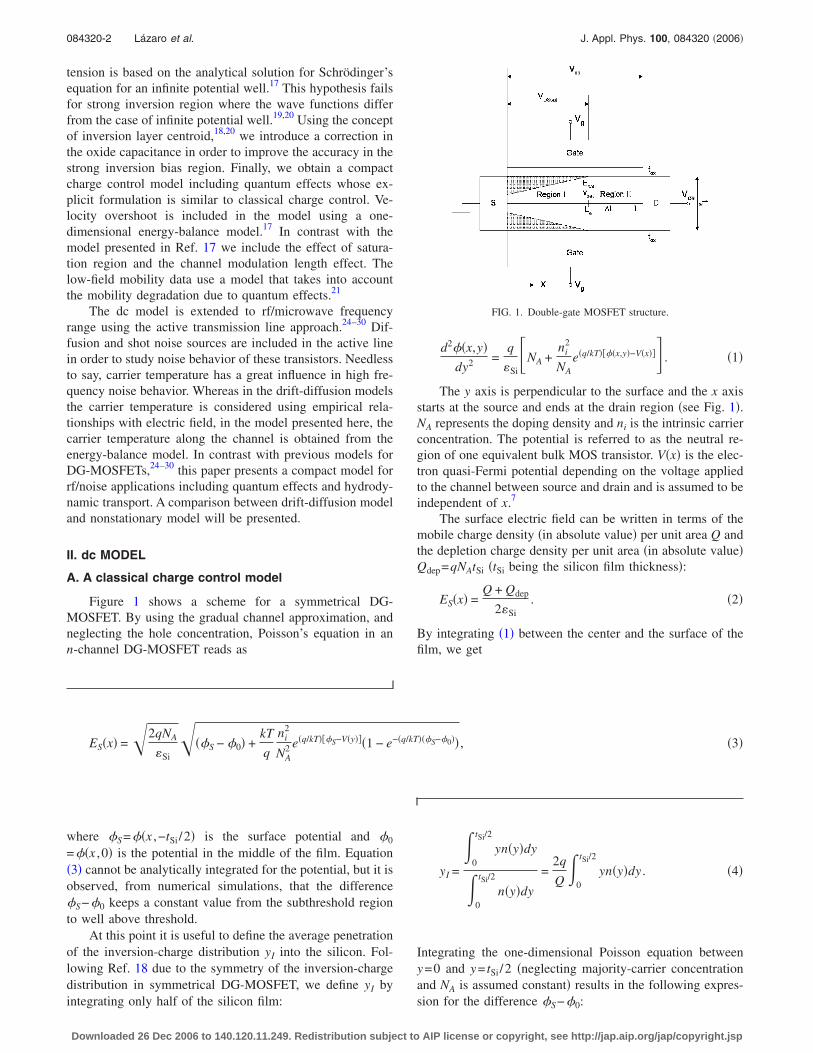
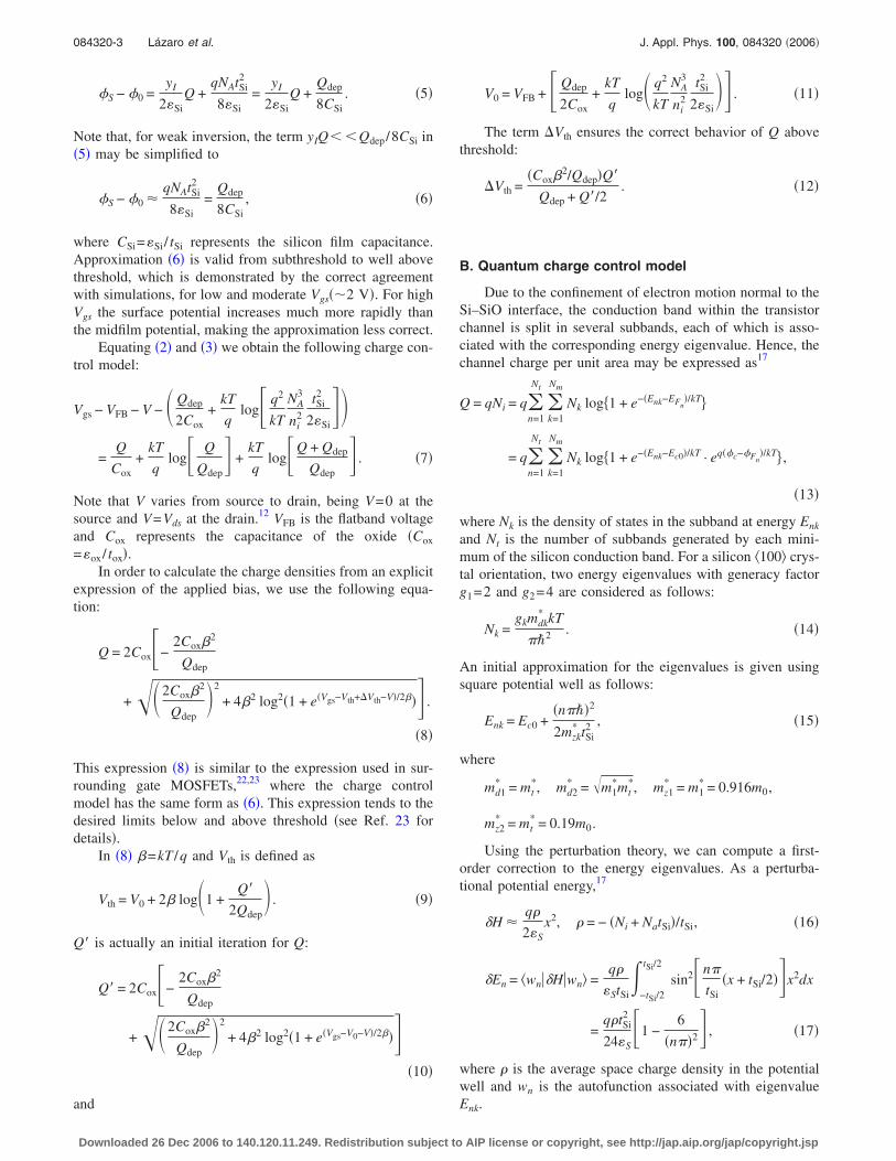
To verify the compact quantum-effect model, we comparepredictions with those obtained with SCHRED,16 which nu-merically and self-consistently solves the Poisson andSchrödinger equations in arbitrary 1D MOS structures. Fig-ures 2 and 3 show the inversion charge as a function of gatebias for a DG-MOSFET ��M =4.05 eV, tox=1.5 nm� withtSi=5 nm, NA=1017 cm−3 �Fig. 2�, and tSi=10 nm, NA
=1017 cm−3 �Fig. 3�. These figures compare the classicalsimulation �Poisson equation solved numerically withSCHRED� and the self-consistent Poisson-Schrödinger simula-tion with the classical compact model ��8�–�12�� and thecompact model �18�. This figure shows an excellent agree-ment between the classical simulation and the classical com-pact model ��8�–�12��, validating approximation �6�. Never-theless, the quantum compact model ��13�–�17�� and thesimplified expression �18� do not agree with numerical simu-lations in the strong inversion region, but the agreement is
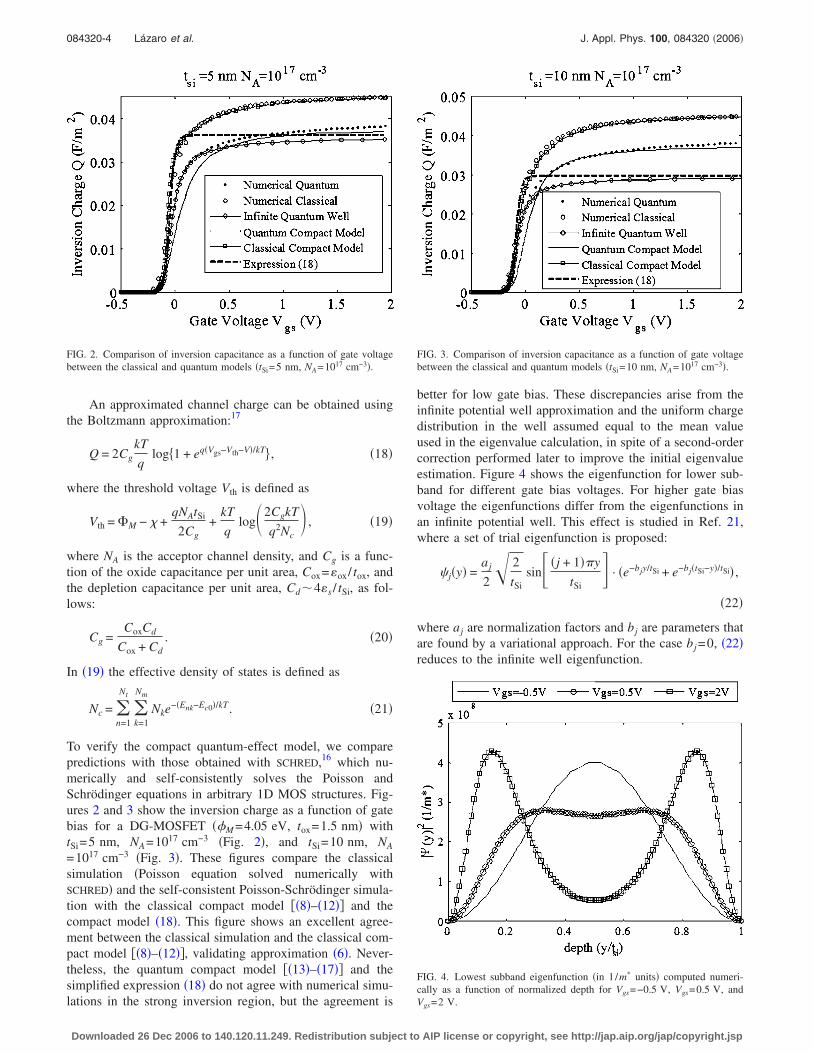
better for low gate bias. These discrepancies arise from theinfinite potential well approximation and the uniform chargedistribution in the well assumed equal to the mean valueused in the eigenvalue calculation, in spite of a second-ordercorrection performed later to improve the initial eigenvalueestimation. Figure 4 shows the eigenfunction for lower sub-band for different gate bias voltages. For higher gate biasvoltage the eigenfunctions differ from the eigenfunctions inan infinite potential well. This effect is studied in Ref. 21,where a set of trial eigenfunction is proposed:
j�y� =aj
2� 2
tSisin� �j + 1��y
tSi� · �e−bjy/tSi + e−bj�tSi−y�/tSi� ,
�22�
where aj are normalization factors and bj are parameters thatare found by a variational approach. For the case bj =0, �22�reduces to the infinite well eigenfunction.
FIG. 2. Comparison of inversion capacitance as a function of gate voltagebetween the classical and quantum models �tSi=5 nm, NA=1017 cm−3�.
FIG. 3. Comparison of inversion capacitance as a function of gate voltagebetween the classical and quantum models �tSi=10 nm, NA=1017 cm−3�.
FIG. 4. Lowest subband eigenfunction �in 1 /m* units� computed numeri-cally as a function of normalized depth for Vgs=−0.5 V, Vgs=0.5 V, andVgs=2 V.
084320-4 Lázaro et al. J. Appl. Phys. 100, 084320 �2006�
Downloaded 26 Dec 2006 to 140.120.11.249. Redistribution subject to AIP license or copyright, see http://jap.aip.org/jap/copyright.jsp
Integrating Poisson’s equation over half the Si filmyields18
Q = 2Cox* �Vgs − �MS − �0 −
Qdep
2Cox�1 +
Cox
4CSi��
= 2Cox* �Vgs − Vth� , �23�
with
Cox* =
Cox
1 + Cox�yI/�Si�. �24�
Equation �23� is accurate in weak, moderate, and strong in-version regions due to the fact that no simplified assumptionshave been made in its deduction. Note that Vth is a nearlyconstant threshold voltage for strong-inversion conditions.
Equation �23� can be interpreted as a surface potentialformulation for DG-MOSFET devices. However, the inver-sion centroid is a function of the inversion charge Q. As aresult a nonlinear equation that does not have an explicitsolution is obtained. In the classical compact model, i.e., yI
=0, Cox* reduces to Cox.
A simple relationship between inversion centroid and in-version charge obtained by fitting numerical simulation re-sults is given by18
1
yI=
1
a + btSi+
1
yI0� NI
NI0�n
, �25�
with a=0.35 nm, b=0.26, yI0=6 nm, NI0=7�1012 cm−2,and n=0.8.
Using a variational method and an eigenfunction �22�, analternative explicit expression to �25� is given in Ref. 21.
From results of Figs. 2 and 3, we propose using the samecharge compact model to include quantum effects but usingthe effective oxide capacitance Cox
* , which is calculated using�24� and �25� from an initial iteration in the inversion chargegiven by �13�. This unified compact model has the sameexplicit expression for classical and quantum-effect modelsbut using different threshold voltages �see Figs. 2 and 3� andeffective oxide capacitance.
Figures 2 and 3 compare the explicit quantum chargemodel with numerical simulation performed with SCHRED.16
A good agreement is obtained in all inversion regions withthe explicit compact model, especially in the strong inversionregion, whereas the model given by expressions �13�–�17�and the explicit model �18� fail.
C. Drain current model
In extremely short-channel DG-MOSFET the channel isquasiballistic, thus an important overshoot velocity isexpected.4,9,17 Using a simplified energy-balance model, theelectron mobility is a function of the electron temperaturerelated to the average energy of the carriers. The electrontemperature Te is governed by the following equation:
dTe
dx+
Te − T0
�w= −
q
2kEx�x� , �26�
where the energy-relaxation length is defined as �w
2vsat�w, �w being the energy relaxation time and vsat the
saturation velocity. Equation �26� can be integrated assuminga constant �w, under boundary condition Te�x=0�=T0, andthe x component of the electric field expressed as a functionof channel potential, Ex�x�=−dV�x� /dx, as follows:
Te�x� = T0 +q
2kV�x� −
q
2k�w�
0
x
V���e��−y�/�wd� . �27�
The velocity increases along the channel, and for VdsVdss
�called saturation voltage�, the velocity reaches a saturationvelocity. Assuming that the velocity is saturated we can di-vide the channel into two sections �see Fig. 1�: the first sec-tion, 0�x�Le=L−Lsat, and the saturation region, x�Le. Incontrast with classical drift-diffusion models, the saturatedvelocity in the saturation region due to nonstationary effectscan achieve several times the stationary saturation velocity,vsat. This phenomenon is known as velocity overshoot. In thelinear region, the carrier velocity can be obtained from themobility as follows:
v�x� = �n�x�Ex�x� =�n0
1 + ��Te�x� − T0�Ex�x� , �28�
where the value of � is determined from �26� under staticconditions, where dTe /dx=0:
� =2k�n0
q�wvsat. �29�
The dependence of the mobility �n0 on normal electricfield is often referred to as mobility reduction, whereas thedependence on lateral electric field is often referred to asvelocity saturation. The effective vertical field Eeff reducesthe effective mobility given by the model:19
�n0�tSi,Eeff�
=U0
1 + �U0/�ph�bulk�����ph�bulk�/�ph�tSi�eff��� − 1� + �
U0
�sr
,
�30�
where effective U0 and � are fitting parameters, and the ef-fective normal field is given by
Eeff Q + Qdep
4�Si. �31�
Note that the model �30� takes into account the dependenceof mobility with silicon thickness due to the variation of thedistance between the inversion-charge centroid and the sur-face with respect to tSi. Model �30� uses the lowest subbandassociated with eigenfunction �22� to calculate the phononlimited mobility. Screening mobility is modeled as in con-ventional devices using the effective field ��sr�Eeff
−2�.Expression �28� differs from the classical drift-diffusion
model, where the mobility is a function of lateral electricfield as follows:
084320-5 Lázaro et al. J. Appl. Phys. 100, 084320 �2006�
Downloaded 26 Dec 2006 to 140.120.11.249. Redistribution subject to AIP license or copyright, see http://jap.aip.org/jap/copyright.jsp
�n =�n0
1 + Ex/Esat, Ex � Esat, �32�
where Esat is the saturation field when the velocity reachessaturation voltage.
For the calculation of the current that flows from drain tosource, the so-called channel current Ids, it is assumed thatthe hole current as well as recombination/generation can beneglected. The channel current can be described by drift-diffusion current as follows:
Ids = WQv , �33�
where W is the gate width.Using the charge control models previously presented
and the velocity given by �28�, the drain current in the linearchannel region can be obtained as follows:
Ids =
W�0
Vdsat
�n0Q�V�dV
�0
Le
�1 + ��Te�x� − T0��dx
=
W�eff�0
Vdsat
Q�V�dV
�0
Le
�1 + ��Te�x� − T0��dx
. �34�
The numerator integral can be calculated numerically or us-ing the mean value theorem and can be expressed as a func-tion of mean effective mobility, �eff, whose value can beobtained by means of numerical integration of �34�. Alterna-tively, some authors for compact modeling propose the useof the following empirical expression for the mean effectivemobility:
�eff =�0
1 + ���Vgs − Vth�
�n0�tSi,Eeff�x = 0� + Eeff�x = Le�
2� , �35�
where �� is an empirical parameter. Other approximation as-sumes a smoothing change of the mobility along the channel,thus the effective mobility is given by �30� but evaluated atthe mean effective field between the source and the satura-tion point.
In the classical case, using effective mobility, the chargeintegral in �34� can be evaluated and the integration can bedone analytically �37�, being denoted as the functionf�Vgs ,Vdssat�.
From �3� and �4� we get
dV = −dQ
Cox−
kT
q�dQ
Q+
dQ
Q + Qdep� . �36�
Therefore the expression of IDS can be written in termsof carrier charge densities. Integrating the charge density us-ing �8�, between Qs and Qd �Q=Qs at the source end andQ=Qd at the saturation point or drain end�, we have
f�Vgs,Vdssat� = 2�2kT
q�Qs − Qd� +
Qs2 − Qd
2
2Cox
+kT
qQdep log�Qd + Qdep
Qs + Qdep�� . �37�
In the quantum case, using effective mobility, the chargeintegral in �34� can be evaluated numerically, and it is de-noted by the function f�Vgs ,Vdssat�.
In order to evaluate the integral of the denominator of�34�, we need to know the temperature profile along thechannel. As an approximation, in the linear region we cansuppose that the lateral field is linear from a small value atthe source end to the saturation field at x=Le �Ex=Esatx /Le�.Using �37�, we obtain
Ids =W�efff�Vgs,Vdss�
Le + �q�/2k��0
Le
V���e��−Le�/�wd�
=W
Le
�efff�Vgs,Vdss�1 + �nVdss
, �38�
where
�n =�eff
vsatLe
1
�1 + 2�w/Le��39�
and Vdss is equal to Vds for nonsaturated channels �Le=L� andVdss=Vdssat for saturated channels.
Channel length modulation should also be included. ForVds�Vdssat, the device works in the linear region, Le=L andVdssat=Vds. For Vds�Vdssat, the channel is partially saturated,and the saturated channel length is given by
�L = L − Le = Lc arcsin h�Vds − Vdssat
EsatLc� , �40�
where Lc=a�c is proportional to the characteristic length�c,
30 and a is a fitting parameter �0�a�1�.The saturation voltage Vdssat is found using the current
continuity along the channel. Equating �17� with the expres-sion of the current in the saturated channel,
Ids = WQ�V = Vdssat�vsat,ns, �41�
where vsat,ns is the channel velocity in the saturation region�x�Le� taking into account the nonstationary effect from�26�. The value of Vdssat can be found by equaling to 0 thederivative of Ids vs Vds:
17
Vdssat = Vdssat�wi� +
kT
qln�1 + exp�q�Vdssat
�si� − Vdssat�wi� �/kT�� ,
�42�
where Vdssat in the strong inversion �si� and weak inversion�wi� bias regions is given by
Vdssatsi = � 1
�n��1 + 2�n�Vgs − Vth�� , Vgs − Vth � 0
Vgs − Vth, Vgs − Vth � 0,� �43�
084320-6 Lázaro et al. J. Appl. Phys. 100, 084320 �2006�
Downloaded 26 Dec 2006 to 140.120.11.249. Redistribution subject to AIP license or copyright, see http://jap.aip.org/jap/copyright.jsp
Vdssatwi 4kT/q , �44�
where �n=�eff / �vsatL�.A smoothing function is used to interpolate Vdss:
Vdss = Vds −kT
q
ln�1 + exp�A�Vds − Vdssat�/�kT/q���A
, �45�
where A is the parameter that controls the transition betweensaturated and nonsaturated channels.
Note that the lateral electric field in the saturation regionis given by
Ex�x� = Esat cosh� x − Le
Lc� , �46�
where Esat is the field at saturation channel point and is ob-tained from Vdssat, under linear field approximation in thelinear region. Using �46� and �27�, the carrier temperature inthe saturation region can be calculated.
The conventional drift-diffusion model using mobility-field relation �32� is recovered if �w is set to 0, then vsat,ns isequal to stationary value vsat, and �n=�n.
III. RF AND NOISE MODELING
The existing noise calculation methodologies �namely,the Klaassen-Prins approach, equivalent circuit method, andimpedance field method� must be adapted to model the noisein short-channel devices. A generalization of the long-channel noise calculation methods to incorporate the mobil-ity degradation is described in Ref. 31. This reference showsthe equivalence between these noise calculation methods inthe presence of velocity saturation.
In order to take into account the most important effects,such as non-quasi-stationary effects, the gate and drain cor-relation between noise sources, and the tunneling gate cur-rent noise, we use the segmentation method. This method hasbeen used for noise modeling in other devices such as metal-semiconductor field-effect transistors �MESFETs�, high elec-tron mobility transistors �HEMTs�, MOSFETs, single-gateSOI devices,25 and DG-MOSFETs.28–30
In the segmentation method or active transmission lineanalysis, the channel is divided into channel sections orslides. The small-signal and noise sources for each channelsection can be derived from semiconductor equations. Thesegmentation method can be considered as an efficientimplementation or discretization to calculate these integralscompatible with rf computed-aided-design tools. Moreover,the segmentation method allows us to incorporate other noisesources such as the shot noise introduced by the gate currentand the small-signal calculation including non-quasi-staticeffects.
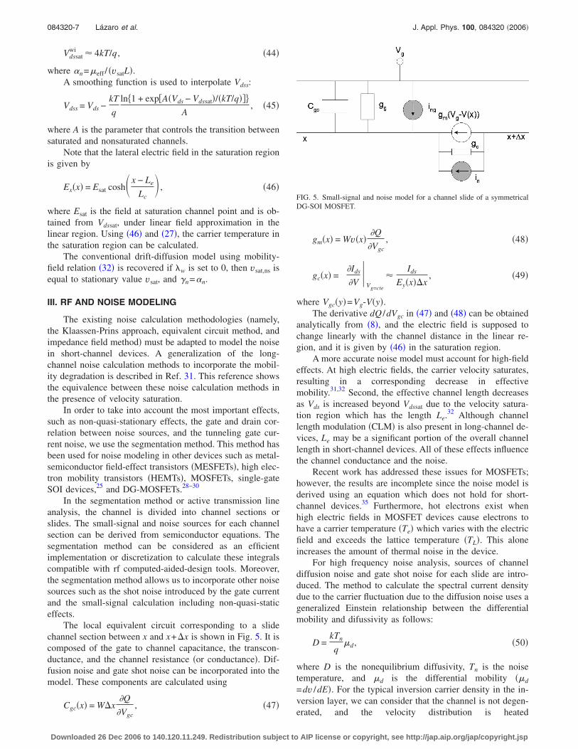
The local equivalent circuit corresponding to a slidechannel section between x and x+�x is shown in Fig. 5. It iscomposed of the gate to channel capacitance, the transcon-ductance, and the channel resistance �or conductance�. Dif-fusion noise and gate shot noise can be incorporated into themodel. These components are calculated using
Cgc�x� = W�x�Q
�Vgc, �47�
gm�x� = Wv�x��Q
�Vgc, �48�
gc�x� = � �Ids
�V�
Vg=cte
Ids
Ey�x��x, �49�
where Vgc�y�=Vg-V�y�.The derivative dQ /dVgc in �47� and �48� can be obtained
analytically from �8�, and the electric field is supposed tochange linearly with the channel distance in the linear re-gion, and it is given by �46� in the saturation region.
A more accurate noise model must account for high-fieldeffects. At high electric fields, the carrier velocity saturates,resulting in a corresponding decrease in effectivemobility.31,32 Second, the effective channel length decreasesas Vds is increased beyond Vdssat due to the velocity satura-tion region which has the length Le.
32 Although channellength modulation �CLM� is also present in long-channel de-vices, Le may be a significant portion of the overall channellength in short-channel devices. All of these effects influencethe channel conductance and the noise.
Recent work has addressed these issues for MOSFETs;however, the results are incomplete since the noise model isderived using an equation which does not hold for short-channel devices.35 Furthermore, hot electrons exist whenhigh electric fields in MOSFET devices cause electrons tohave a carrier temperature �Te� which varies with the electricfield and exceeds the lattice temperature �TL�. This aloneincreases the amount of thermal noise in the device.
For high frequency noise analysis, sources of channeldiffusion noise and gate shot noise for each slide are intro-duced. The method to calculate the spectral current densitydue to the carrier fluctuation due to the diffusion noise uses ageneralized Einstein relationship between the differentialmobility and difussivity as follows:
D =kTn
q�d, �50�
where D is the nonequilibrium diffusivity, Tn is the noisetemperature, and �d is the differential mobility ��d
=dv /dE�. For the typical inversion carrier density in the in-version layer, we can consider that the channel is not degen-erated, and the velocity distribution is heated
FIG. 5. Small-signal and noise model for a channel slide of a symmetricalDG-SOI MOSFET.
084320-7 Lázaro et al. J. Appl. Phys. 100, 084320 �2006�
Downloaded 26 Dec 2006 to 140.120.11.249. Redistribution subject to AIP license or copyright, see http://jap.aip.org/jap/copyright.jsp
Maxwellian.33–35 Under this assumption the noise tempera-ture Tn becomes equal to the carrier temperature Te, and thespectral current density can be written as33
Sin�x� = in2 = 4qWQ
D
�x= 4kTe�x�gc�x� . �51�
Under high channel electric fields, the temperature of elec-trons in the channel can rise above that of the lattice. Thiseffect can increase the thermal noise of the device.32 In thehydrodynamic model presented here, Te�x� is obtained from�36� and �27�.
However, in the drift-diffusion models an analytical re-lationship between Te and the lateral field Ey�y� must beused. One of the more challenging aspects of including theeffect of electron temperature in the noise model is finding agood model for the electron temperature. A prevalent modelin the literature expresses the electron mobility as a functionof the temperature as shown below:36
�eff = �0�TL
Te. �52�
Mobility can also be represented as a function of electricfield:35
�eff =�0
�1 + �Ex/Ec�2. �53�
Equation �53� presents a slightly more complex and moreaccurate relationship than the piecewise function normallyused. Equating the two and solving for Te /TL give
Te = TL�1 + � E
Ec�2� . �54�
Note that the channel conductance of each slide can be cal-culated from �49� and �53� as follows:35
gc�x� =WQ
�x�d =
WQ��eff + �eff� Ex��x
, �eff� = dv/dEx.
�55�
Using �53� and the expression for differential channel con-ductance gc �55�, we can obtain a compact expression for thecurrent noise spectral density between x and x+�x as fol-lows:
Sin�x� = in2 = 4k
�0TL
�1 + �E/Ec�2
WQ�x��x
. �56�
However, ultrathin oxides below 4 nm exhibit drastic in-crease of leakage current, the so-called direct tunnelingcurrent.29,37,38 In this regime, the gate oxide capacitor intro-duces a shot noise current source, besides two classical noisesources: drain and gate current noise. The impact of the di-rect tunneling current on high frequency noise performanceis becoming critical. The gate shot noise current generated ineach segment of the MOSFET flows along the channel andsubsequently creates drain shot noise current as well, be-cause it is uncorrelated with the origins of the drain and gatecurrent noise. Since the direct tunneling current can be sub-stantial, the drain shot noise becomes comparable to the
drain current noise in MOSFETs with oxides below 2 nm.27
The tunneling gate current �TGC� for each channel slide isgiven by direct tunneling current theory37,38 as follows:
Jn�y� = AEox�y�2e−B�1−�1 − �Vox�y�/�b��3/2�/Eox�y�, �57�
with the electric field within the oxide Eox�y� equal to
Eox�y� = E�y��S
�ox=
Q + Qdep
�ox, �58�
where Vox�y� is the voltage across the oxide �Vox�y�=Eox�y�tox�, and �b the barrier height equal to 3.1 eV.38 Theconstants A and B are given in Ref. 38.
The small signal conductance gg�y� associated with thetunneling current is given by
gg�y� = W�y�Jn�y��Eox�x�
·�Eox�y�
�Vg. �59�
Using nodal admittance method the active transmission linecan be analyzed.30 We start numbering the circuit nodes fromsource 1 �node 1� to drain end �node N+1�, and the gate isnumbered as N+2. The current at circuit nodes can be writ-ten as
�Ii� = �Yij� · �Vi� + �in,i� , �60�
where Ii is the signal input current at each circuit node, Vi isthe node voltage, In,i is the noise current at each node, and Yij
is the admittance matrix.The current at the internal nodes is equal to zero �Ii,=0
for i=2, . . . ,N� and the external nodes are connected to volt-age bias.
To obtain the external admittance and correlation matrix,the nodes are renumbered as internal nodes �i=2, . . . ,N� andexternal nodes �nodes 1, N+1, N+2�. Then, the equationsystem �60� can be written as
�0�
Ie� = �Yii Yie
Yei Yee� · �Vi
Ve� + � ini
ine� . �61�
The correlation matrix between noise sources at each nodecan be expressed as
C = � ini
ine� · � ini
ine�†
= �Cii Cie
Cei Cee� . �62�
Assuming that the channel noise source and shot noisesource are uncorrelated, the correlation matrix is computedfrom �51� and 2qJg�x��x, respectively.
The intrinsic transistor admittance matrix, Y int, is givenby
Ie = Y intVe + ie, �63�
Y int = Yee − PYie, �64�
ie = �ig
id� = ine − Pini, �65�
where
084320-8 Lázaro et al. J. Appl. Phys. 100, 084320 �2006�
Downloaded 26 Dec 2006 to 140.120.11.249. Redistribution subject to AIP license or copyright, see http://jap.aip.org/jap/copyright.jsp
P = YeiYii−1. �66�
Using �61�–�64�, the admittance equivalent noise sources �ig,id� can be found, and the associated correlation matrix is theintrinsic transistor correlation matrix CYi given by
CYi = � ig2 ig
*id
igid* id
2 � = Cee − CeiP† − PCie + PCiiP
†. �67�
Equation �67� expresses the contribution of each channelnoise source to the total noise �including the correlation co-efficient� affected by a factor that can be interpreted as ageneralized impedance field.
The intrinsic small-signal equivalent circuit elements�Fig. 6� can be obtained from intrinsic Y parameters by iden-tification. In order to obtain the transistor S parameters andnoise parameters, the series parasitic resistances and induc-tance and the parallel parasitic capacitance must be included.The extrinsic �including parasitic� parameters are obtainedusing well-known relations described in Refs. 39 and 40
For rf applications the goals are maximizing the intrinsicgain, cutoff frequency fT, and maximum frequency of oscil-lation fmax. From the equivalent circuit of Fig. 6 these pa-rameters can be easily calculated with the followingexpressions:27
fT =gm
2�Cgs�1 + 2Cgd/Cgs
gm
2��Cgs + Cgd�, �68�
fmax gm
2�Cgs�4�Rs + Ri + Rg��gds + gm�Cgd/Cgs��
, �69�
where Cgs and Cgd includ fringing and overlap capacitancescalculated using expressions given in Ref. 41 gm is the gatetransconductance, Ri �in series with Cgs� takes into accountthe distributed nature of the MOSFET, and gds is the drain-to-source conductance. As shown in �68� and �69�, fT de-pends on the ratio gm and total gate capacitance, while fmax
also depends on the source/drain and gate parasitic resis-
tances and the ratio Cgd /Cgs. The Overlap and fringing ca-pacitances increase intrinsic capacitances, reducing the cut-off frequency fT and the maximum frequency of oscillation,fmax.
Parasitic resistances reduce fmax and increase transistornoise. The gate resistance consists of two major contribu-tions: one contribution is the well-known silicide sheetresistance.24 The other contribution is the contact resistancebetween silicide and polysilicon.25 The gate resistance isgiven by 42
Rg =1
3
RsheetW
LNfingers2 Ncontacts
2 +con
WL, �70�
where Rsheet is the silicide gate sheet resistance, Nfingers andNcontacts are the number of parallel fingers and gate contacts,and con is the silicide-to-polysilicon specific contact resis-tance. A typical value for silicide sheet resistance is 2–5� / sq and a typical value for con is 20 � �m2.42 In thispaper, for device simulation, a lower bound by gate resis-tance in device scaling is considered using values of Rsheet
=2 � / sq and con=0. A distributed contact resistance modelis employed for source �drain� access resistance.
IV. SIMULATED RESULTS
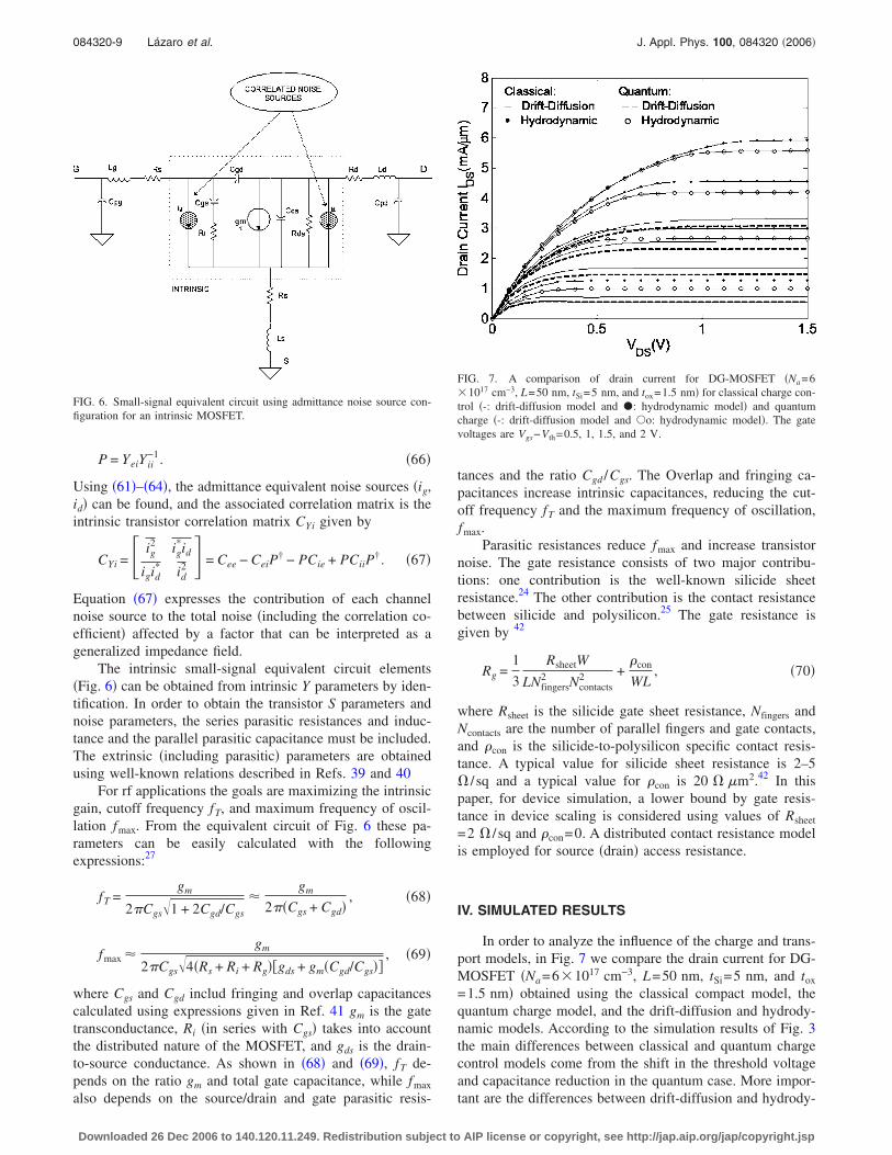
In order to analyze the influence of the charge and trans-port models, in Fig. 7 we compare the drain current for DG-MOSFET �Na=6�1017 cm−3, L=50 nm, tSi=5 nm, and tox
=1.5 nm� obtained using the classical compact model, thequantum charge model, and the drift-diffusion and hydrody-namic models. According to the simulation results of Fig. 3the main differences between classical and quantum chargecontrol models come from the shift in the threshold voltageand capacitance reduction in the quantum case. More impor-tant are the differences between drift-diffusion and hydrody-
FIG. 6. Small-signal equivalent circuit using admittance noise source con-figuration for an intrinsic MOSFET.
FIG. 7. A comparison of drain current for DG-MOSFET �Na=6�1017 cm−3, L=50 nm, tSi=5 nm, and tox=1.5 nm� for classical charge con-trol �-: drift-diffusion model and �: hydrodynamic model� and quantumcharge �-: drift-diffusion model and �o: hydrodynamic model�. The gatevoltages are Vgs−Vth=0.5, 1, 1.5, and 2 V.
084320-9 Lázaro et al. J. Appl. Phys. 100, 084320 �2006�
Downloaded 26 Dec 2006 to 140.120.11.249. Redistribution subject to AIP license or copyright, see http://jap.aip.org/jap/copyright.jsp
namic models. Due to overshoot effect the velocity, the cur-rent, and transconductance are larger in the hydrodynamicmodels than in the drift-diffusion model.
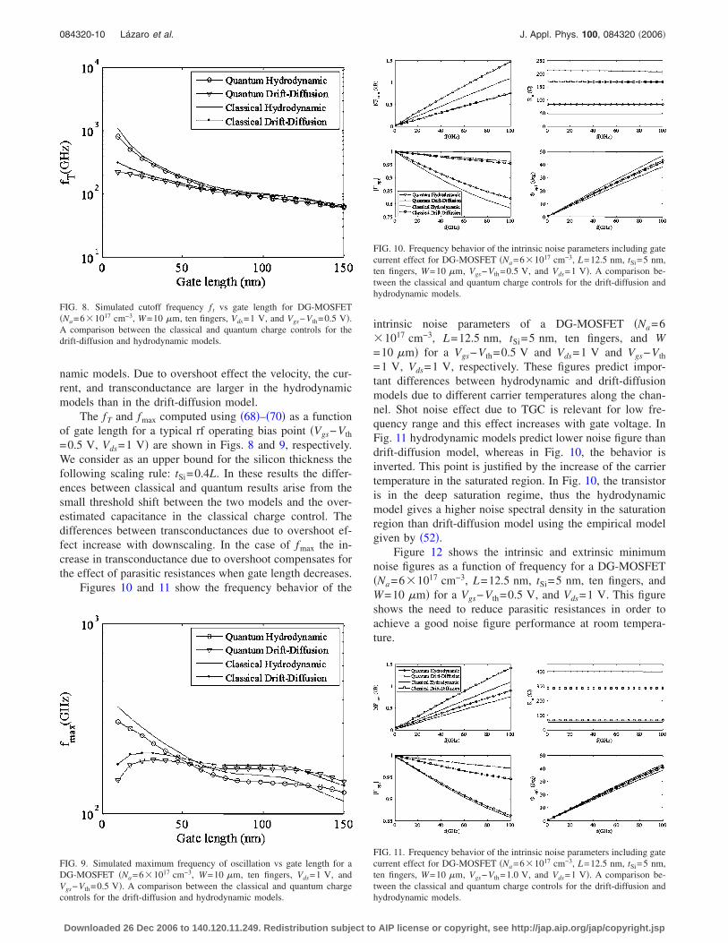
The fT and fmax computed using �68�–�70� as a functionof gate length for a typical rf operating bias point �Vgs−Vth
=0.5 V, Vds=1 V� are shown in Figs. 8 and 9, respectively.We consider as an upper bound for the silicon thickness thefollowing scaling rule: tSi=0.4L. In these results the differ-ences between classical and quantum results arise from thesmall threshold shift between the two models and the over-estimated capacitance in the classical charge control. Thedifferences between transconductances due to overshoot ef-fect increase with downscaling. In the case of fmax the in-crease in transconductance due to overshoot compensates forthe effect of parasitic resistances when gate length decreases.
Figures 10 and 11 show the frequency behavior of the
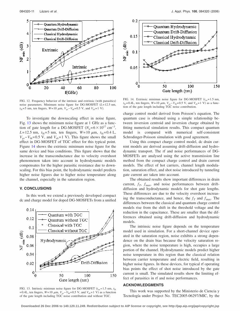
intrinsic noise parameters of a DG-MOSFET �Na=6�1017 cm−3, L=12.5 nm, tSi=5 nm, ten fingers, and W=10 �m� for a Vgs−Vth=0.5 V and Vds=1 V and Vgs−Vth
=1 V, Vds=1 V, respectively. These figures predict impor-tant differences between hydrodynamic and drift-diffusionmodels due to different carrier temperatures along the chan-nel. Shot noise effect due to TGC is relevant for low fre-quency range and this effect increases with gate voltage. InFig. 11 hydrodynamic models predict lower noise figure thandrift-diffusion model, whereas in Fig. 10, the behavior isinverted. This point is justified by the increase of the carriertemperature in the saturated region. In Fig. 10, the transistoris in the deep saturation regime, thus the hydrodynamicmodel gives a higher noise spectral density in the saturationregion than drift-diffusion model using the empirical modelgiven by �52�.
Figure 12 shows the intrinsic and extrinsic minimumnoise figures as a function of frequency for a DG-MOSFET�Na=6�1017 cm−3, L=12.5 nm, tSi=5 nm, ten fingers, andW=10 �m� for a Vgs−Vth=0.5 V, and Vds=1 V. This figureshows the need to reduce parasitic resistances in order toachieve a good noise figure performance at room tempera-ture.
FIG. 8. Simulated cutoff frequency f t vs gate length for DG-MOSFET�Na=6�1017 cm−3, W=10 �m, ten fingers, Vds=1 V, and Vgs−Vth=0.5 V�.A comparison between the classical and quantum charge controls for thedrift-diffusion and hydrodynamic models.
FIG. 9. Simulated maximum frequency of oscillation vs gate length for aDG-MOSFET �Na=6�1017 cm−3, W=10 �m, ten fingers, Vds=1 V, andVgs−Vth=0.5 V�. A comparison between the classical and quantum chargecontrols for the drift-diffusion and hydrodynamic models.
FIG. 10. Frequency behavior of the intrinsic noise parameters including gatecurrent effect for DG-MOSFET �Na=6�1017 cm−3, L=12.5 nm, tSi=5 nm,ten fingers, W=10 �m, Vgs−Vth=0.5 V, and Vds=1 V�. A comparison be-tween the classical and quantum charge controls for the drift-diffusion andhydrodynamic models.
FIG. 11. Frequency behavior of the intrinsic noise parameters including gatecurrent effect for DG-MOSFET �Na=6�1017 cm−3, L=12.5 nm, tSi=5 nm,ten fingers, W=10 �m, Vgs−Vth=1.0 V, and Vds=1 V�. A comparison be-tween the classical and quantum charge controls for the drift-diffusion andhydrodynamic models.
084320-10 Lázaro et al. J. Appl. Phys. 100, 084320 �2006�
Downloaded 26 Dec 2006 to 140.120.11.249. Redistribution subject to AIP license or copyright, see http://jap.aip.org/jap/copyright.jsp
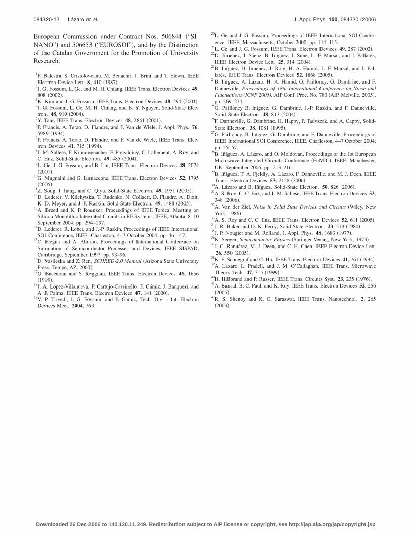
To investigate the downscaling effect in noise figure,Fig. 13 shows the minimum noise figure at 1 GHz as a func-tion of gate length for a DG-MOSFET �Na=6�1017 cm−3,L=12.5 nm, tSi=5 nm, ten fingers, W=10 �m, tSi=0.4 L,Vgs−Vth=0.5 V, and Vds=1 V�. This figure shows the smalleffect in DG-MOSFET of TGC effect for this typical point.Figure 14 shows the extrinsic minimum noise figure for thesame device and bias conditions. This figure shows that theincrease in the transconductance due to velocity overshootphenomenon taken into account in hydrodynamic modelscompensates for the higher parasitic resistance due to down-scaling. For this bias point, the hydrodynamic model predictshigher noise figures due to higher noise temperature alongthe channel, especially in the saturation region.
V. CONCLUSIONS
In this work we extend a previously developed compactdc and charge model for doped DG-MOSFETs from a unified
charge control model derived from Poisson’s equation. Thequantum case is obtained using a simple relationship be-tween inversion centroid and inversion charge obtained byfitting numerical simulation results. This compact quantummodel is compared with numerical self-consistentSchrodinger-Poisson simulation with good agreement.
Using this compact charge control model, dc drain cur-rent models are derived assuming drift-diffusion and hydro-dynamic transport. The rf and noise performances of DG-MOSFETs are analysed using the active transmission linemethod from the compact charge control and drain currentmodels. The effect of hot carriers, channel length modula-tion, saturation effect, and shot noise introduced by tunnelinggate current are taken into account.
The obtained results show important differences in draincurrent, fT, fmax, and noise performances between drift-diffusion and hydrodynamic models for shot gate lengths.These differences are due to the velocity overshoot increas-ing the transconductance, and hence, the fT and fmax. Thedifferences between the classical and quantum charge controlmodels rise from the shift in the threshold voltage and thereduction in the capacitance. These are smaller than the dif-ferences obtained using drift-diffusion and hydrodynamicmodels.
The intrinsic noise figure depends on the temperaturemodel used in simulation. For a short-channel device oper-ated in the saturation region, noise exhibits a strong depen-dence on the drain bias because the velocity saturation re-gion, where the noise temperature is high, occupies a largeportion of the channel. Hydrodynamic models predict highernoise temperature in this region than the classical relationbetween carrier temperature and electric field, resulting inhigher noise figures. In these devices, for typical rf operatingbias points the effect of shot noise introduced by the gatecurrent is small. The simulated results show the limiting ef-fect of parasitics in rf and noise performances.
ACKNOWLEDGMENTS
This work was supported by the Ministerio de Ciencia yTecnología under Project No. TEC2005-06297/MIC, by the
FIG. 12. Frequency behavior of the intrinsic and extrinsic �with parasitics�noise parameters. Minimum noise figure for DG-MOSFET �L=12.5 nm,tSi=5 nm, ten fingers, W=10 �m, Vgs−Vth=0.5 V, and Vds=1 V�.
FIG. 13. Intrinsic minimun noise figure for DG-MOSFET �tox=1.5 nm, tSi
=0.4L, ten fingers, W=10 �m, Vgs−Vth=0.5 V, and Vds=1 V� as a functionof the gate length including TGC noise contribution and without TGC.
FIG. 14. Extrinsic minimun noise figure for DG-MOSFET �tox=1.5 nm,tSi=0.4L, ten fingers, W=10 �m, Vgs−Vth=0.5 V, and Vds=1 V� as a func-tion of the gate length including TGC noise contribution.
084320-11 Lázaro et al. J. Appl. Phys. 100, 084320 �2006�
Downloaded 26 Dec 2006 to 140.120.11.249. Redistribution subject to AIP license or copyright, see http://jap.aip.org/jap/copyright.jsp
European Commission under Contract Nos. 506844 �“SI-NANO”� and 506653 �“EUROSOI”�, and by the Distinctionof the Catalan Government for the Promotion of UniversityResearch.
1F. Balestra, S. Cristoloveanu, M. Benachir, J. Brini, and T. Elewa, IEEEElectron Device Lett. 8, 410 �1987�.
2J. G. Fossum, L. Ge, and M. H. Chiang, IEEE Trans. Electron Devices 49,808 �2002�.
3K. Kim and J. G. Fossum, IEEE Trans. Electron Devices 48, 294 �2001�.4J. G. Fossum, L. Ge, M. H. Chiang, and B. Y. Nguyen, Solid-State Elec-tron. 48, 919 �2004�.
5Y. Taur, IEEE Trans. Electron Devices 48, 2861 �2001�.6P. Francis, A. Terao, D. Flandre, and F. Van de Wiele, J. Appl. Phys. 76,5989 �1994�.
7P. Francis, A. Terao, D. Flandre, and F. Van de Wiele, IEEE Trans. Elec-tron Devices 41, 715 �1994�.
8J.-M. Sallese, F. Krummenacher, F. Pregaldiny, C. Lallement, A. Roy, andC. Enz, Solid-State Electron. 49, 485 �2004�.
9L. Ge, J. G. Fossum, and B. Liu, IEEE Trans. Electron Devices 48, 2074�2001�.
10G. Mugnaini and G. Iannaccone, IEEE Trans. Electron Devices 52, 1795�2005�.
11Z. Song, J. Jiang, and C. Qiyu, Solid-State Electron. 49, 1951 �2005�.12D. Lederer, V. Kilchytska, T. Rudenko, N. Collaert, D. Flandre, A. Dixit,
K. D. Meyer, and J.-P. Raskin, Solid-State Electron. 49, 1488 �2005�.13A. Breed and K. P. Roenker, Proceedings of IEEE Topical Meeting on
Silicon Monolithic Integrated Circuits in RF Systems, IEEE, Atlanta, 8–10September 2004, pp. 294–297.
14D. Lederer, R. Lobet, and J.-P. Raskin, Proceedings of IEEE InternationalSOI Conference, IEEE, Charleston, 4–7 October 2004, pp. 46—47.
15C. Fiegna and A. Abrano, Proceedings of International Conference onSimulation of Semiconductor Processes and Devices, IEEE SISPAD,Cambridge, September 1997, pp. 93–96.
16D. Vasileska and Z. Ren, SCHRED-2.0 Manual �Arizona State UniversityPress, Tempe, AZ, 2000�.
17G. Baccarani and S. Reggiani, IEEE Trans. Electron Devices 46, 1656�1999�.
18J. A. López-Villanueva, P. Cartujo-Cassinello, F. Gámiz, J. Banqueri, andA. J. Palma, IEEE Trans. Electron Devices 47, 141 �2000�.
19V. P. Trivedi, J. G. Fossum, and F. Gamiz, Tech. Dig. - Int. ElectronDevices Meet. 2004, 763.
20L. Ge and J. G. Fossum, Proceedings of IEEE International SOI Confer-ence, IEEE, Massachusetts, October 2000, pp. 114–115.
21L. Ge and J. G. Fossum, IEEE Trans. Electron Devices 49, 287 �2002�.22D. Jiménez, J. Sáenz, B. Iñíguez, J. Suñé, L. F. Marsal, and J. Pallarès,
IEEE Electron Device Lett. 25, 314 �2004�.23B. Iñíguez, D. Jiménez, J. Roig, H. A. Hamid, L. F. Marsal, and J. Pal-
larès, IEEE Trans. Electron Devices 52, 1868 �2005�.24B. Iñíguez, A. Lázaro, H. A. Hamid, G. Pailloncy, G. Dambrine, and F.
Danneville, Proceedings of 18th International Conference on Noise andFluctuations (ICNF 2005), AIP Conf. Proc. No. 780 �AIP, Melville, 2005�,pp. 269–274.
25G. Pailloncy B. Iníguez, G. Dambrine, J.-P. Raskin, and F. Danneville,Solid-State Electron. 48, 813 �2004�.
26F. Danneville, G. Dambrine, H. Happy, P. Tadyszak, and A. Cappy, Solid-State Electron. 38, 1081 �1995�.
27G. Pailloncy, B. Iñíguez, G. Dambrine, and F. Danneville, Proceedings ofIEEE International SOI Conference, IEEE, Charleston, 4–7 October 2004,pp. 55–57.
28B. Iñíguez, A. Lázaro, and O. Moldovan, Proceedings of the 1st EuropeanMicrowave Integrated Circuits Conference �EuMIC�, IEEE, Manchester,UK, September 2006, pp. 213–216.
29B. Iñíguez, T. A. Fjeldly, A. Lázaro, F. Danneville, and M. J. Deen, IEEETrans. Electron Devices 53, 2128 �2006�.
30A. Lázaro and B. Iñíguez, Solid-State Electron. 50, 826 �2006�.31A. S. Roy, C. C. Enz, and J.-M. Sallese, IEEE Trans. Electron Devices 53,
348 �2006�.32A. Van der Ziel, Noise in Solid State Devices and Circuits �Wiley, New
York, 1986�.33A. S. Roy and C. C. Enz, IEEE Trans. Electron Devices 52, 611 �2005�.34J. R. Baker and D. K. Ferry, Solid-State Electron. 23, 519 �1980�.35J. P. Nougier and M. Rolland, J. Appl. Phys. 48, 1683 �1977�.36K. Seeger, Semiconductor Physics �Springer-Verlag, New York, 1973�.37J. C. Ranuárez, M. J. Deen, and C.-H. Chen, IEEE Electron Device Lett.
26, 550 �2005�.38K. F. Schuegraf and C. Hu, IEEE Trans. Electron Devices 41, 761 �1994�.39A. Lázaro, L. Pradell, and J. M. O’Callaghan, IEEE Trans. Microwave
Theory Tech. 47, 315 �1999�.40H. Hillbrand and P. Russer, IEEE Trans. Circuits Syst. 23, 235 �1976�.41A. Bansal, B. C. Paul, and K. Roy, IEEE Trans. Electron Devices 52, 256
�2005�.42R. S. Shenoy and K. C. Saraswat, IEEE Trans. Nanotechnol. 2, 265
�2003�.
084320-12 Lázaro et al. J. Appl. Phys. 100, 084320 �2006�
Downloaded 26 Dec 2006 to 140.120.11.249. Redistribution subject to AIP license or copyright, see http://jap.aip.org/jap/copyright.jsp
Related Documents