624 IEEE TRANSACTIONS ON ELECTRON DEVICES, VOL. 55, NO. 2, FEBRUARY 2008 A Compact Model Satisfying Gummel Symmetry in Higher Order Derivatives and Applicable to Asymmetric MOSFETs Guan Huei See, Student Member, IEEE, Xing Zhou, Senior Member, IEEE, Karthik Chandrasekaran, Siau Ben Chiah, Zhaomin Zhu, Chengqing Wei, Shihuan Lin, Guojun Zhu, and Guan Hui Lim, Student Member, IEEE Abstract—This paper presents a new concept for the MOSFET saturation voltages at the drain and source sides referenced to bulk, and applies them to the popularly used smoothing functions for the effective drain–source voltage (V ds,eff ). The proposed model not only builds in physically all the terminal-bias variations, but is also extended to include source/drain asymmetry in real devices in a single-core compact model. The new model resolves a key bottleneck in existing models for passing the Gummel symme- try test (GST) in higher order derivatives, which has to be traded off for the geometry-dependent V ds,eff smoothing parameter. The complete drain-current model, including the effects of velocity saturation and overshoot as well as source/drain series resistance, has also been reformulated with the same “bulk-referencing” concept. It is shown that the proposed model passes the GST in all higher order derivatives without any constraint on the value of the smoothing parameter. It also demonstrates potential extension to modeling asymmetric MOSFETs, which is becoming an important model capability. Index Terms—Asymmetric source/drain, compact model, effec- tive drain–source voltage, Gummel symmetry test (GST), higher order derivative, MOSFET. I. INTRODUCTION S OURCE and drain symmetry is a fundamental feature of an ideal MOSFET. The Gummel symmetry test (GST) [1] was introduced as a benchmark test to qualify a MOSFET compact model, which requires the drain–source current I ds (V ds ) to be strictly an odd function of V ds . In the GST, the source and drain terminals are to be biased at certain potential plus/minus a varying voltage V x , and it is required that the even- order derivatives of I ds w.r.t. V x be smoothly passing through Manuscript received July 5, 2007; revised October 15, 2007. This work was supported in part by Nanyang Technological University under Grant RGM30/03 and in part by the Semiconductor Research Corporation under Grant 2004-VJ- 1166G. The review of this paper was arranged by Editor H. Jaouen. G. H. See, X. Zhou, Z. M. Zhu, C. Q. Wei, S. H. Lin, G. J. Zhu, and G. H. Lim are with the School of Electrical and Electronic Engineer- ing, Nanyang Technological University, Singapore 639798, Singapore (e-mail: [email protected]; [email protected]; [email protected]; weic0002@ ntu.edu.sg; [email protected]; [email protected]; limg0013@ntu. edu.sg). K. Chandrasekaran was with Nanyang Technological University, Singapore 639798, Singapore. He is with the Advanced Micro Devices, Inc., Sunnyvale, CA 94088 USA (e-mail: [email protected]). S. B. Chiah was with Nanyang Technological University, Singapore 639798, Singapore. He is with the Chartered Semiconductor Manufacturing Ltd., Singapore 738406, Singapore (e-mail: [email protected]). Color versions of one or more of the figures in this paper are available online at http://ieeexplore.ieee.org. Digital Object Identifier 10.1109/TED.2007.912951 V x = 0. Besides the “odd function” requirement, in order to pass the GST with nth-order derivative, it is also necessary that d ( n ) I ds (0) ≡ d n I ds (V x )/dV n x |V x→0 exist (i.e., no singularity at V x = 0) [2]. It has been recognized [3] that Gummel symmetry was one of the main showstoppers in the industry de facto stan- dard model BSIM3 [4]. Special care has been taken in passing the GST in the next-generation standard model PSP [5]. How- ever, Gummel symmetry at higher order derivatives, which is often required for distortion analyses [2], [6], still remains a problem due to the use of the mathematical smoothing func- tion for the “effective drain–source voltage” (V ds, eff ), which has to be traded off for the appropriate range of the smoothing parameter for modeling geometry-dependent output (drain cur- rent and drain conductance) characteristics, or by introducing extra parameter for Gummel symmetry. In addition, almost all existing models are developed based on swapping source and drain terminals whenever V ds < 0, as commonly implemented in all circuit simulators, which is based on MOS convention and applies only to ideal MOSFETs with perfect source/drain structural symmetry. In this paper, we present a simple modification in the com- monly used smoothing functions for the effective drain–source voltage, with the essential change from a “source-referenced” to a “bulk-referenced” saturation-voltage model. We apply this idea in a simple drain-current model to verify its functionality. We demonstrate that the proposed model satisfies the GST with any higher order derivatives while maintaining physical scaling with all terminal biases. In addition, it is also possible to ex- tend the model to include physical asymmetry in source/drain structures of a MOSFET in the same core model. II. EXISTING AND PROPOSED MODELS Most contemporary MOS compact models use a mathemati- cal function for the effective drain–source voltage that smoothly joins the linear and saturation regions of operation. The two commonly used mathematical functions to be discussed are ϑ 1 {V ds ,V ds, sat ; a x }≡ V ds [1 + (V ds /V ds, sat ) a x ] 1/a x (1) ϑ 2 {V ds ,V ds, sat ; δ s }≡ V ds, sat − 1 2 V ds, sat − V ds − δ s + (V ds, sat − V ds − δ s ) 2 +4δ s V ds, sat (2) 0018-9383/$25.00 © 2008 IEEE

Welcome message from author
This document is posted to help you gain knowledge. Please leave a comment to let me know what you think about it! Share it to your friends and learn new things together.
Transcript
624 IEEE TRANSACTIONS ON ELECTRON DEVICES, VOL. 55, NO. 2, FEBRUARY 2008
A Compact Model Satisfying Gummel Symmetryin Higher Order Derivatives and Applicable
to Asymmetric MOSFETsGuan Huei See, Student Member, IEEE, Xing Zhou, Senior Member, IEEE, Karthik Chandrasekaran, Siau Ben Chiah,
Zhaomin Zhu, Chengqing Wei, Shihuan Lin, Guojun Zhu, and Guan Hui Lim, Student Member, IEEE
Abstract—This paper presents a new concept for the MOSFETsaturation voltages at the drain and source sides referenced tobulk, and applies them to the popularly used smoothing functionsfor the effective drain–source voltage (Vds,eff ). The proposedmodel not only builds in physically all the terminal-bias variations,but is also extended to include source/drain asymmetry in realdevices in a single-core compact model. The new model resolves akey bottleneck in existing models for passing the Gummel symme-try test (GST) in higher order derivatives, which has to be tradedoff for the geometry-dependent Vds,eff smoothing parameter. Thecomplete drain-current model, including the effects of velocitysaturation and overshoot as well as source/drain series resistance,has also been reformulated with the same “bulk-referencing”concept. It is shown that the proposed model passes the GST in allhigher order derivatives without any constraint on the value of thesmoothing parameter. It also demonstrates potential extension tomodeling asymmetric MOSFETs, which is becoming an importantmodel capability.
Index Terms—Asymmetric source/drain, compact model, effec-tive drain–source voltage, Gummel symmetry test (GST), higherorder derivative, MOSFET.
I. INTRODUCTION
SOURCE and drain symmetry is a fundamental feature ofan ideal MOSFET. The Gummel symmetry test (GST) [1]
was introduced as a benchmark test to qualify a MOSFETcompact model, which requires the drain–source current Ids
(Vds) to be strictly an odd function of Vds . In the GST, thesource and drain terminals are to be biased at certain potentialplus/minus a varying voltage Vx , and it is required that the even-order derivatives of Ids w.r.t. Vx be smoothly passing through
Manuscript received July 5, 2007; revised October 15, 2007. This work wassupported in part by Nanyang Technological University under Grant RGM30/03and in part by the Semiconductor Research Corporation under Grant 2004-VJ-1166G. The review of this paper was arranged by Editor H. Jaouen.
G. H. See, X. Zhou, Z. M. Zhu, C. Q. Wei, S. H. Lin, G. J. Zhu,and G. H. Lim are with the School of Electrical and Electronic Engineer-ing, Nanyang Technological University, Singapore 639798, Singapore (e-mail:[email protected]; [email protected]; [email protected]; [email protected]; [email protected]; [email protected]; [email protected]).
K. Chandrasekaran was with Nanyang Technological University, Singapore639798, Singapore. He is with the Advanced Micro Devices, Inc., Sunnyvale,CA 94088 USA (e-mail: [email protected]).
S. B. Chiah was with Nanyang Technological University, Singapore 639798,Singapore. He is with the Chartered Semiconductor Manufacturing Ltd.,Singapore 738406, Singapore (e-mail: [email protected]).
Color versions of one or more of the figures in this paper are available onlineat http://ieeexplore.ieee.org.
Digital Object Identifier 10.1109/TED.2007.912951
Vx = 0. Besides the “odd function” requirement, in order topass the GST with nth-order derivative, it is also necessary thatd(n)Ids(0) ≡ dnIds(Vx)/dV n
x |Vx→0 exist (i.e., no singularity atVx = 0) [2]. It has been recognized [3] that Gummel symmetrywas one of the main showstoppers in the industry de facto stan-dard model BSIM3 [4]. Special care has been taken in passingthe GST in the next-generation standard model PSP [5]. How-ever, Gummel symmetry at higher order derivatives, which isoften required for distortion analyses [2], [6], still remains aproblem due to the use of the mathematical smoothing func-tion for the “effective drain–source voltage” (Vds,eff ), whichhas to be traded off for the appropriate range of the smoothingparameter for modeling geometry-dependent output (drain cur-rent and drain conductance) characteristics, or by introducingextra parameter for Gummel symmetry. In addition, almost allexisting models are developed based on swapping source anddrain terminals whenever Vds < 0, as commonly implementedin all circuit simulators, which is based on MOS conventionand applies only to ideal MOSFETs with perfect source/drainstructural symmetry.
In this paper, we present a simple modification in the com-monly used smoothing functions for the effective drain–sourcevoltage, with the essential change from a “source-referenced”to a “bulk-referenced” saturation-voltage model. We apply thisidea in a simple drain-current model to verify its functionality.We demonstrate that the proposed model satisfies the GST withany higher order derivatives while maintaining physical scalingwith all terminal biases. In addition, it is also possible to ex-tend the model to include physical asymmetry in source/drainstructures of a MOSFET in the same core model.
II. EXISTING AND PROPOSED MODELS
Most contemporary MOS compact models use a mathemati-cal function for the effective drain–source voltage that smoothlyjoins the linear and saturation regions of operation. The twocommonly used mathematical functions to be discussed are
ϑ1 {Vds, Vds,sat ; ax} ≡ Vds
[1 + (Vds/Vds,sat)ax ]1/ax(1)
ϑ2 {Vds, Vds,sat ; δs} ≡ Vds,sat −12
(Vds,sat − Vds − δs
+√
(Vds,sat − Vds − δs)2 + 4δsVds,sat
)(2)
0018-9383/$25.00 © 2008 IEEE
SEE et al.: COMPACT MODEL SATISFYING GUMMEL SYMMETRY IN HOD 625
where ax and δs are smoothing parameters for the respec-tive smoothing functions. ϑ2(x) in (2) is known to havecaused asymmetry as it is obviously not an odd function ofVds , whereas ϑ1(x) in (1) is strictly an odd function whenconsidering terminal swapping for negative Vds (as imple-mented in most circuit simulators). However, when Gummelsymmetry at higher order derivatives becomes important, (1)has shown a major limitation, since to avoid singularities in thenth-order derivative at Vx = 0, ax has to be larger than n dueto the (Vds /Vds,sat)ax −n term, but short-channel devices oftenrequire a small value of ax . Hence, channel-length-dependentax and higher order Gummel symmetry have to be traded offand, very often, both cannot be satisfied at the same time,especially for short-channel devices passing the higher orderGST. It is, therefore, highly desirable to have a smoothingfunction that passes the GST with any order of derivatives.
In (1) and (2), Vds,sat is, in fact, referenced to sourceby the MOSFET convention, i.e., saturation occurs only atthe drain side, and drain current always flows from drain tosource. We propose a simple modification of (2) [Vds,eff =ϑ2(Vds, Vds,sat ; δs)] based on “bulk reference” for the new ef-fective drain–source voltage:
Vds,eff = Vdb,eff − Vsb,eff (3)
where
Vdb,eff = ϑ2 {Vdb , Vdb,sat ; δs} (3a)
and
Vsb,eff = ϑ2 {Vsb , Vsb,sat ; δs} (3b)
are the effective drain and source voltages referenced to bulk,respectively. The two saturation voltages at the drain and source,Vdb,sat and Vsb,sat , are given by
Vdb,sat = Vds,sat + Vsb (4a)
Vsb,sat = Vsd,sat + Vdb (4b)
where Vds,sat is the drain–source saturation voltage (evaluatedat the source side) and Vsd,sat is the source–drain saturationvoltage (evaluated at the drain side). The essence of this simplemodification is from a “source-referenced” (Vds,eff and Vds,sat)model to a “bulk-referenced” model, in which all formulationsrelating the source and drain are bulk-referenced. As will beshown next, (4a) and (4b) is the key (new) model, satisfying theGST as well as physically building in terminal-bias variationsin a compact model. Unlike conventional compact models inwhich source and drain are defined by the MOSFET conven-tion and drain terminal voltage is always higher than sourceterminal voltage for nMOS, the source and drain terminals aretreated as node labels (designated by layout), in which Vds canbe negative and the source/drain terminals are not swapped inmodel evaluation. This requires the Ids model to be a strict oddfunction of Vds and capable of evaluation with negative Vds .Therefore, the saturation voltages at the drain and source sidesare to be modeled separately, which is also another key featureand advantage of this approach. This model framework allows
modeling of MOSFETs with intrinsic source/drain asymmetrydue, e.g., to process variations or special asymmetric device de-signs, which can never be handled easily by models based onsource/drain terminal swapping.
There are many ways to determine the saturation voltage;we simply take the conventional threshold-voltage-based ap-proach [7] to demonstrate the idea used in (4a) and (4b). Thesaturation voltage is defined as the channel voltage where Ids
reaches the saturation current, Idsat (i.e., reaching saturationvelocity vsat). It can be determined by the intercept point ofthe linear and saturation currents. The saturation current (afterTaylor expansion at the source end) can be written as
Idsat = vsatWCox(Vgt,s − Ab,s∆φ) (5)
where Vgt,s = Qi,s/Cox is the inversion charge normalized tothe oxide capacitance Cox , evaluated at the source end
Vgt,s = Υ√
φs(0) + vthe[φs (0)−2φF −Vs b ]/v t h − Υ√
φs(0)(6)
Ab,s = 1 +Υ
2√
φs(0)(7)
is the bulk-charge factor, and
∆φ = φs(L) − φs(0) (8)
is the surface potential difference between the drainφs(L)(Vcb = Vdb) and source φs(0)(Vcb = Vsb). The variableΥ = (2qεSiNch)1/2/Cox is the body factor, φF is the bulk Fermipotential, and vth is the thermal voltage. The linear drift currentplus diffusion current (after Taylor expansion at the source end)is given by
Idd,s = µeff 0CoxW
L
(Vgt,s −
Ab,s∆φ
2+ Ab,svth
)∆φ (9)
where
µeff 0 =µ0
1 + Vds/(LEsat)(9a)
is the lateral field mobility based on the piecewise velocity–fieldrelation [8], µ0 is the vertical field mobility, and
Esat =2vsat
µ0(9b)
is the saturation field. Based on the “pinned” surface potentialapproximations, φs(y) ≈ 2φF + Vcb(y) where Vcb is the chan-nel voltage w.r.t. bulk, (8) can be approximated as
∆φ ≈ (2φF + Vdb) − (2φF + Vsb) = Vds. (10)
Solving (5) and (9) at Vds = Vds,sat together with (10), thesaturation voltage is obtained as
Vds,sat =Vgt,sLEsat
Vgt,s + Ab,sLEsat + 2Ab,svth(11)
where the 2Ab,svth term in the denominator comes from the dif-fusion current, which is not included in conventional saturation-voltage expressions. The previous derivation is, in fact, “source-referenced” as the Taylor expansion is done at the source end.
626 IEEE TRANSACTIONS ON ELECTRON DEVICES, VOL. 55, NO. 2, FEBRUARY 2008
The onset of saturation actually happens at the drain side(“drain” by label in the layout) in “forward” operation whenVdb > Vsb ; therefore, from the convention Vds = Vdb − Vsb , itis possible to define the “saturation drain voltage” w.r.t. bulk asVds,sat = Vdb,sat − Vsb , which gives the model in (4a). Vsb isstill the terminal voltage since, in forward mode, the “source”side is still not being pinched off (Vgs > Vgd = Vt).
Similarly, an equivalent analysis for the “drain” side leads toa set of equations evaluated at the drain end, which is applicableto “reverse” mode when Vsb > Vdb , as follows:
Vgt,d = Υ√
φs(L) + vthe[φs (L)−2φF −Vd b ]/v t h − Υ√
φs(L)
(12)
Ab,d = 1 +Υ
2√
φs(L)(13)
Vsd,sat =Vgt,dLEsat
Vgt,d + Ab,dLEsat + 2Ab,dvth. (14)
Equation (14) gives the onset of saturation at the “source” (label)side, which can be similarly written as Vsd,sat = Vsb,sat − Vdb ,giving the proposed (4b) for the “saturation source voltage”w.r.t. bulk. Now, it can be easily proved that the new effectivedrain–source voltage in (3) is strictly an odd function of Vds
with no singularities in higher order derivatives at Vx = 0.There are other necessary conditions for the GST in the drain-
current model, as discussed in [3], [9]–[11]. We simply formu-late the proposed Vds,eff in (3) into a simple surface-potential-based Ids model to verify its functionality. For more complexsurface-potential-based drain-current models in which accuratesolutions of surface potentials are needed, minor adjustment inthe inversion charge in (6) and (12) is required for the correctsubthreshold current behavior. The drain-current model used fordemonstration in this paper is derived similarly to symmetricbulk-charge linearization [9] and, applying the approximationin (10), is given as
Ids0 = β(qi + Abvth)Vds,eff (15)
where
qi = Vgb − VFB − φs − Υ√
φs (16)
Ab = 1 +Υ
2√
φs
(17)
φs =φseff (0) + φseff (L)
2(18)
where VFB is the flatband voltage and Vgb = Vg − Vb , andφseff (0) and φseff (L) are the effective surface potentials at thesource and drain side, respectively, by replacing Vsb and Vdb
with Vsb,eff and Vdb,eff when evaluating the Vcb term in thesurface potentials. We use our unified regional φseff (Vcb) so-lutions [12], [13] in this paper, although other explicit/iterativeφs(Vcb) solutions can also be used. β = µeff 0CoxW/L in (15)is an “averaged” gain factor arising from lateral field mobilitiesevaluated at the source and drain
µeff 0 =µeff 0,s + µeff 0,d
2(19)
which is based on the piecewise velocity–field relation [8], butreformulated as
µeff 0,s =µ0
1 + δLVsb,eff /(LEsat)(19a)
µeff 0,d =µ0
1 + δLVdb,eff /(LEsat). (19b)
It is based on the similar idea as (3) for a consistent “bulk-referenced” model to maintain Ids being a strict odd functionof Vds . δL [10] is introduced as a fitting parameter. The verticalfield mobility µ0 is from [7], in which the effective field isobtained from the average inversion and depletion charges
Eeff =1
φs(L) − φs(0)
∫ φs (L)
φs (0)Eeff (y)dφs(y)
=1
∆φεSi
[∫ φs (L)
φs (0)ζnQi dφs +
∫ φs (L)
φs (0)Qb dφs
]
=Cox
∆φεSi
{∫ φs (L)
φs (0)ζn [Vgt − Ab(φs − φs)]dφs
+Υ∫ φs (L)
φs (0)
[√φs +
1
2√
φs
(φs − φs)
]dφs
}
=Coxζn
εSi
(Vgt +
ζb
ζnΥ
√φs
)(20)
Vgt =Vgt,s + Vgt,d
2(20a)
where ζn and ζb are fitting parameters.The short-channel equivalent set of equations used in this
paper is given in the Appendix, which scales with gate lengthfor all geometries.
III. RESULTS AND DISCUSSION
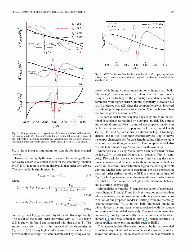
GSTs are performed on (1) and (3), which is a necessarycondition for the Ids model to pass the GST in this paper.Results for two values of the respective smoothing parame-ters, ax = 2.5; 3.5 and δs = 0.01; 0.05, are shown in Fig. 1by sweeping Vx with a 5 mV step size, with Vg = 1.2 V, Vd =0.5 Vgb + Vx, Vs = 0.5 Vgb − Vx, and Vb = 0 (see Fig. 1 in-set for the GST circuit). All model equations are based onthe same set of core equations shown in Section II and theAppendix with device parameters from a 90 nm technology(oxide thickness tox = 2 nm, channel doping concentrationNch = 6.8 × 1017 cm−3 , channel length L = 10 µm) unlessotherwise explicitly stated. It can be seen that the proposedVds,eff in (3) passes zero Vx smoothly for all second-, fourth-,and sixth-order derivatives in a fairly large range of δs varia-tions needed for practical smoothing. Although the model in(1) passed the conventional GST (second-order derivative), itobviously failed in the fourth-order derivative with three zerocrossings, implying a glitch in the third-order derivative due tothe singularity of the (Vds/Vds,sat)ax −3 term in the third-orderderivative. For the sixth-order derivative, a singularity existseven for ax = 3.5, which would give a very abrupt transition in
SEE et al.: COMPACT MODEL SATISFYING GUMMEL SYMMETRY IN HOD 627
Fig. 1. Comparison of the proposed model (3) (thick solid/dotted lines) withthe existing model (1) (thin solid/dashed lines) for the following derivatives ofthe GST for two smoothing parameters as indicated from the respective models.(a) Second-order. (b) Fourth-order. (c) Sixth-order. Inset of (a): GST circuit.
Vds,eff from linear to saturation, not suitable for short-channeldevices.
However, if we apply the same idea as in formulating (3), onecan easily construct a similar model for the smoothing functionϑ1(x) in (1) to remove the singularity at higher order derivatives.The new model is simply given by
Vds,eff = Vdbe − Vsbe (21)
where
Vdbe = ϑ1{Vdb , Vdb,sat ; ax} ≡ Vdb
[1 + (Vdb/Vdb,sat)ax ]1/ax
(21a)
Vsbe = ϑ1{Vsb , Vsb,sat ; ax} ≡ Vsb
[1 + (Vsb/Vsb,sat)ax ]1/ax
(21b)
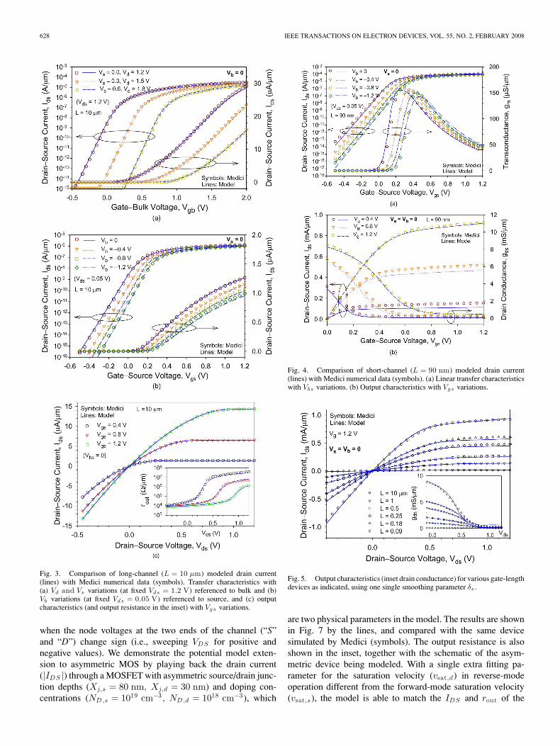
and Vdb,sat and Vsb,sat are given by (4a) and (4b), respectively.The result of the fourth-order derivative with ax = 2.5 using(21) is shown in Fig. 2 and compared with that using (1). Thesmooth transition is due to the removal of the singularity atVds = 0 in (21) for any higher order derivatives, as can be easilyproved mathematically. This demonstrates that by using our ap-
Fig. 2. GST for the fourth-order derivative based on (21) applying the newconcept to (1), and compared with the original (1), showing removal of thesingularity in (1).
proach of defining two separate saturation voltages (i.e., “bulk-referencing”), one can solve the dilemma in existing modelsusing ϑ1(x) for trading off the geometry-dependent smoothingparameter with higher order Gummel symmetry. However, (3)is still preferred over (21) since the computational cost involvedin evaluating the square-root function in (3) is much lesser thanthat for the power function in (21).
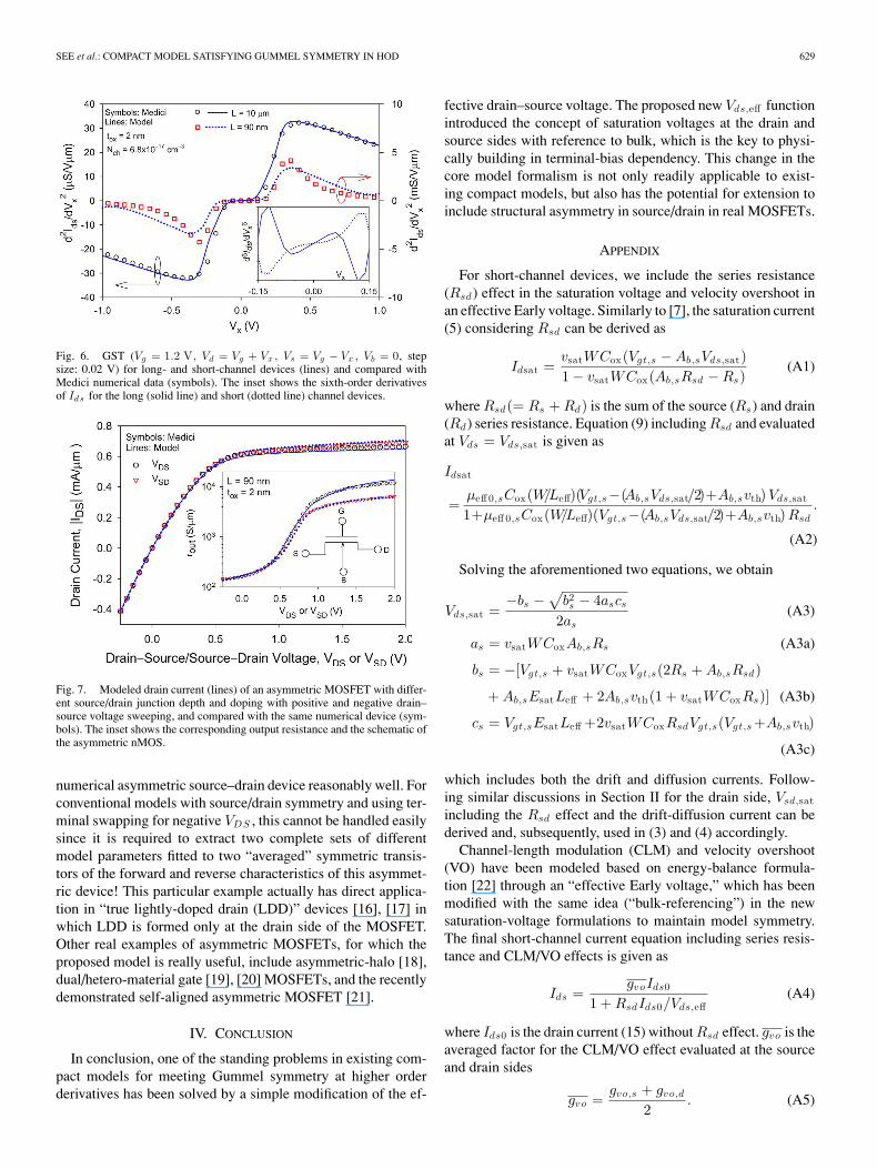
The core model formalism also physically builds in the ter-minal dependency as required by a compact model. The correctand physical terminal-bias scaling of the proposed model canbe further demonstrated by playing back the Ids model withVd, Vs, Vb , and Vg variations, as shown in Fig. 3 for long-channel and in Fig. 4 for short-channel devices. Fig. 5 showsthe output characteristics for gate-length scaling with one singlevalue of the smoothing parameter δs . Our complete model alsoextends to terminal charge/capacitance with symmetry.
Numerical GSTs using Medici have been performed for twodevices, L = 10 µm and 90 nm, also shown in Fig. 6 (sym-bols). Playback for the same devices (lines) using the samemodel equations and parameters (without tuning individual de-vices) in the entire linear/saturation region matches quite wellwith the Medici data. Smooth transitions are also observed inthe sixth-order derivatives of the GST, as shown in the inset ofFig. 6, which guarantees smoothness in all lower order deriva-tives that are often required for higher order harmonic balanceand distortion analyses [6].
Although the new model (3) requires evaluation of two satura-tion voltages (11) and (14) and involves more computations thanwhen evaluating one, it turns out to be the key and a novel con-tribution of our proposed model in shifting from an essentially“source-referenced” Vds,eff to the “bulk-referenced” model inwhich device structural parameters associated with the sourceand drain can be modeled separately. This method to guaranteeGummel symmetry has recently been demonstrated by otherauthors [14] in a way similar to ours [15], which confirms itsdirect application to existing models such as BSIM.
This approach also allows the model to be further extendedto include any intentional or unintentional asymmetry in thesource and drain, e.g., the mismatch current in pass transistors
628 IEEE TRANSACTIONS ON ELECTRON DEVICES, VOL. 55, NO. 2, FEBRUARY 2008
Fig. 3. Comparison of long-channel (L = 10 µm) modeled drain current(lines) with Medici numerical data (symbols). Transfer characteristics with(a) Vd and Vs variations (at fixed Vds = 1.2 V) referenced to bulk and (b)Vb variations (at fixed Vds = 0.05 V) referenced to source, and (c) outputcharacteristics (and output resistance in the inset) with Vg s variations.
when the node voltages at the two ends of the channel (“S”and “D”) change sign (i.e., sweeping VDS for positive andnegative values). We demonstrate the potential model exten-sion to asymmetric MOS by playing back the drain current(|IDS |) through a MOSFET with asymmetric source/drain junc-tion depths (Xj,s = 80 nm, Xj,d = 30 nm) and doping con-centrations (ND,s = 1019 cm−3 , ND,d = 1018 cm−3), which
Fig. 4. Comparison of short-channel (L = 90 nm) modeled drain current(lines) with Medici numerical data (symbols). (a) Linear transfer characteristicswith Vbs variations. (b) Output characteristics with Vg s variations.
Fig. 5. Output characteristics (inset drain conductance) for various gate-lengthdevices as indicated, using one single smoothing parameter δs .
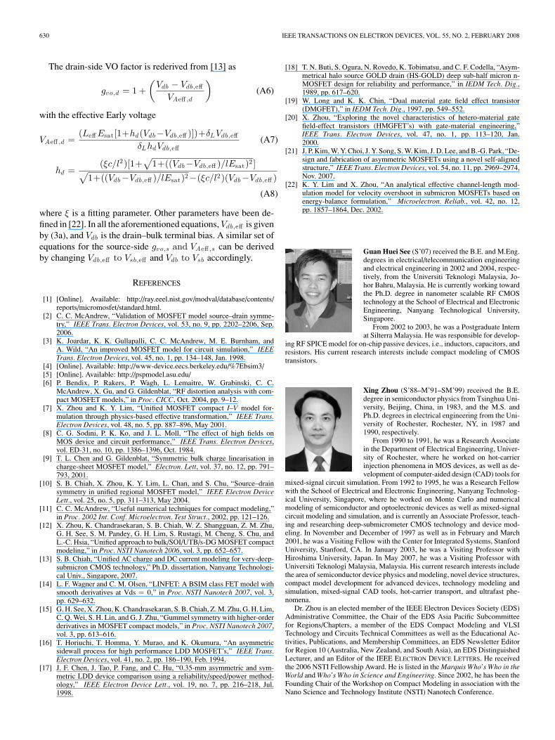
are two physical parameters in the model. The results are shownin Fig. 7 by the lines, and compared with the same devicesimulated by Medici (symbols). The output resistance is alsoshown in the inset, together with the schematic of the asym-metric device being modeled. With a single extra fitting pa-rameter for the saturation velocity (vsat,d ) in reverse-modeoperation different from the forward-mode saturation velocity(vsat,s), the model is able to match the IDS and rout of the
SEE et al.: COMPACT MODEL SATISFYING GUMMEL SYMMETRY IN HOD 629
Fig. 6. GST (Vg = 1.2 V, Vd = Vg + Vx , Vs = Vg − Vx , Vb = 0, stepsize: 0.02 V) for long- and short-channel devices (lines) and compared withMedici numerical data (symbols). The inset shows the sixth-order derivativesof Ids for the long (solid line) and short (dotted line) channel devices.
Fig. 7. Modeled drain current (lines) of an asymmetric MOSFET with differ-ent source/drain junction depth and doping with positive and negative drain–source voltage sweeping, and compared with the same numerical device (sym-bols). The inset shows the corresponding output resistance and the schematic ofthe asymmetric nMOS.
numerical asymmetric source–drain device reasonably well. Forconventional models with source/drain symmetry and using ter-minal swapping for negative VDS , this cannot be handled easilysince it is required to extract two complete sets of differentmodel parameters fitted to two “averaged” symmetric transis-tors of the forward and reverse characteristics of this asymmet-ric device! This particular example actually has direct applica-tion in “true lightly-doped drain (LDD)” devices [16], [17] inwhich LDD is formed only at the drain side of the MOSFET.Other real examples of asymmetric MOSFETs, for which theproposed model is really useful, include asymmetric-halo [18],dual/hetero-material gate [19], [20] MOSFETs, and the recentlydemonstrated self-aligned asymmetric MOSFET [21].
IV. CONCLUSION
In conclusion, one of the standing problems in existing com-pact models for meeting Gummel symmetry at higher orderderivatives has been solved by a simple modification of the ef-
fective drain–source voltage. The proposed new Vds,eff functionintroduced the concept of saturation voltages at the drain andsource sides with reference to bulk, which is the key to physi-cally building in terminal-bias dependency. This change in thecore model formalism is not only readily applicable to exist-ing compact models, but also has the potential for extension toinclude structural asymmetry in source/drain in real MOSFETs.
APPENDIX
For short-channel devices, we include the series resistance(Rsd ) effect in the saturation voltage and velocity overshoot inan effective Early voltage. Similarly to [7], the saturation current(5) considering Rsd can be derived as
Idsat =vsatWCox(Vgt,s − Ab,sVds,sat)1 − vsatWCox(Ab,sRsd − Rs)
(A1)
where Rsd(= Rs + Rd) is the sum of the source (Rs) and drain(Rd ) series resistance. Equation (9) including Rsd and evaluatedat Vds = Vds,sat is given as
Idsat
=µeff 0,sCox(W/Leff)(Vgt,s−(Ab,sVds,sat/2)+Ab,svth) Vds,sat
1+µeff 0,sCox(W/Leff)(Vgt,s−(Ab,sVds,sat/2)+Ab,svth) Rsd.
(A2)
Solving the aforementioned two equations, we obtain
Vds,sat =−bs −
√b2s − 4ascs
2as(A3)
as = vsatWCoxAb,sRs (A3a)
bs = −[Vgt,s + vsatWCoxVgt,s(2Rs + Ab,sRsd)
+ Ab,sEsatLeff + 2Ab,svth(1 + vsatWCoxRs)] (A3b)
cs = Vgt,sEsatLeff +2vsatWCoxRsdVgt,s(Vgt,s +Ab,svth)
(A3c)
which includes both the drift and diffusion currents. Follow-ing similar discussions in Section II for the drain side, Vsd,satincluding the Rsd effect and the drift-diffusion current can bederived and, subsequently, used in (3) and (4) accordingly.
Channel-length modulation (CLM) and velocity overshoot(VO) have been modeled based on energy-balance formula-tion [22] through an “effective Early voltage,” which has beenmodified with the same idea (“bulk-referencing”) in the newsaturation-voltage formulations to maintain model symmetry.The final short-channel current equation including series resis-tance and CLM/VO effects is given as
Ids =gvoIds0
1 + RsdIds0/Vds,eff(A4)
where Ids0 is the drain current (15) without Rsd effect. gvo is theaveraged factor for the CLM/VO effect evaluated at the sourceand drain sides
gvo =gvo,s + gvo,d
2. (A5)
630 IEEE TRANSACTIONS ON ELECTRON DEVICES, VOL. 55, NO. 2, FEBRUARY 2008
The drain-side VO factor is rederived from [13] as
gvo,d = 1 +(
Vdb − Vdb,eff
VAeff ,d
)(A6)
with the effective Early voltage
VAeff ,d =(Leff Esat [1+hd(Vdb−Vdb,eff )])+δLVdb,eff
δLhdVdb,eff(A7)
hd =(ξc/l2)[1+
√1+((Vdb−Vdb,eff )/lEsat)2 ]√
1+((Vdb−Vdb,eff )/lEsat)2−(ξc/l2)(Vdb−Vdb,eff )
(A8)
where ξ is a fitting parameter. Other parameters have been de-fined in [22]. In all the aforementioned equations, Vdb,eff is givenby (3a), and Vdb is the drain–bulk terminal bias. A similar set ofequations for the source-side gvo,s and VAeff ,s can be derivedby changing Vdb,eff to Vsb,eff and Vdb to Vsb accordingly.
REFERENCES
[1] [Online]. Available: http://ray.eeel.nist.gov/modval/database/contents/reports/micromosfet/standard.html.
[2] C. C. McAndrew, “Validation of MOSFET model source–drain symme-try,” IEEE Trans. Electron Devices, vol. 53, no. 9, pp. 2202–2206, Sep.2006.
[3] K. Joardar, K. K. Gullapalli, C. C. McAndrew, M. E. Burnham, andA. Wild, “An improved MOSFET model for circuit simulation,” IEEETrans. Electron Devices, vol. 45, no. 1, pp. 134–148, Jan. 1998.
[4] [Online]. Available: http://www-device.eecs.berkeley.edu/%7Ebsim3/[5] [Online]. Available: http://pspmodel.asu.edu/[6] P. Bendix, P. Rakers, P. Wagh, L. Lemaitre, W. Grabinski, C. C.
McAndrew, X. Gu, and G. Gildenblat, “RF distortion analysis with com-pact MOSFET models,” in Proc. CICC, Oct. 2004, pp. 9–12.
[7] X. Zhou and K. Y. Lim, “Unified MOSFET compact I–V model for-mulation through physics-based effective transformation,” IEEE Trans.Electron Devices, vol. 48, no. 5, pp. 887–896, May 2001.
[8] C. G. Sodini, P. K. Ko, and J. L. Moll, “The effect of high fields onMOS device and circuit performance,” IEEE Trans. Electron Devices,vol. ED-31, no. 10, pp. 1386–1396, Oct. 1984.
[9] T. L. Chen and G. Gildenblat, “Symmetric bulk charge linearisation incharge-sheet MOSFET model,” Electron. Lett, vol. 37, no. 12, pp. 791–793, 2001.
[10] S. B. Chiah, X. Zhou, K. Y. Lim, L. Chan, and S. Chu, “Source–drainsymmetry in unified regional MOSFET model,” IEEE Electron DeviceLett., vol. 25, no. 5, pp. 311–313, May 2004.
[11] C. C. McAndrew, “Useful numerical techniques for compact modeling,”in Proc. 2002 Int. Conf. Microelectron. Test Struct., 2002, pp. 121–126.
[12] X. Zhou, K. Chandrasekaran, S. B. Chiah, W. Z. Shangguan, Z. M. Zhu,G. H. See, S. M. Pandey, G. H. Lim, S. Rustagi, M. Cheng, S. Chu, andL.-C. Hsia, “Unified approach to bulk/SOI/UTB/s-DG MOSFET compactmodeling,” in Proc. NSTI Nanotech 2006, vol. 3, pp. 652–657.
[13] S. B. Chiah, “Unified AC charge and DC current modeling for very-deep-submicron CMOS technology,” Ph.D. dissertation, Nanyang Technologi-cal Univ., Singapore, 2007.
[14] L. F. Wagner and C. M. Olsen, “LINFET: A BSIM class FET model withsmooth derivatives at Vds = 0,” in Proc. NSTI Nanotech 2007, vol. 3,pp. 629–632.
[15] G. H. See, X. Zhou, K. Chandrasekaran, S. B. Chiah, Z. M. Zhu, G. H. Lim,C. Q. Wei, S. H. Lin, and G. J. Zhu, “Gummel symmetry with higher-orderderivatives in MOSFET compact models,” in Proc. NSTI Nanotech 2007,vol. 3, pp. 613–616.
[16] T. Horiuchi, T. Homma, Y. Murao, and K. Okumura, “An asymmetricsidewall process for high performance LDD MOSFET’s,” IEEE Trans.Electron Devices, vol. 41, no. 2, pp. 186–190, Feb. 1994.
[17] J. F. Chen, J. Tao, P. Fang, and C. Hu, “0.35-mm asymmetric and sym-metric LDD device comparison using a reliability/speed/power method-ology,” IEEE Electron Device Lett., vol. 19, no. 7, pp. 216–218, Jul.1998.
[18] T. N. Buti, S. Ogura, N. Rovedo, K. Tobimatsu, and C. F. Codella, “Asym-metrical halo source GOLD drain (HS-GOLD) deep sub-half micron n-MOSFET design for reliability and performance,” in IEDM Tech. Dig.,1989, pp. 617–620.
[19] W. Long and K. K. Chin, “Dual material gate field effect transistor(DMGFET),” in IEDM Tech. Dig., 1997, pp. 549–552.
[20] X. Zhou, “Exploring the novel characteristics of hetero-material gatefield-effect transistors (HMGFET’s) with gate-material engineering,”IEEE Trans. Electron Devices, vol. 47, no. 1, pp. 113–120, Jan.2000.
[21] J. P. Kim, W. Y. Choi, J. Y. Song, S. W. Kim, J. D. Lee, and B.-G. Park, “De-sign and fabrication of asymmetric MOSFETs using a novel self-alignedstructure,” IEEE Trans. Electron Devices, vol. 54, no. 11, pp. 2969–2974,Nov. 2007.
[22] K. Y. Lim and X. Zhou, “An analytical effective channel-length mod-ulation model for velocity overshoot in submicron MOSFETs based onenergy-balance formulation,” Microelectron. Reliab., vol. 42, no. 12,pp. 1857–1864, Dec. 2002.
Guan Huei See (S’07) received the B.E. and M.Eng.degrees in electrical/telecommunication engineeringand electrical engineering in 2002 and 2004, respec-tively, from the Universiti Teknologi Malaysia, Jo-hor Bahru, Malaysia. He is currently working towardthe Ph.D. degree in nanometer scalable RF CMOStechnology at the School of Electrical and ElectronicEngineering, Nanyang Technological University,Singapore.
From 2002 to 2003, he was a Postgraduate Internat Silterra Malaysia. He was responsible for develop-
ing RF SPICE model for on-chip passive devices, i.e., inductors, capacitors, andresistors. His current research interests include compact modeling of CMOStransistors.
Xing Zhou (S’88–M’91–SM’99) received the B.E.degree in semiconductor physics from Tsinghua Uni-versity, Beijing, China, in 1983, and the M.S. andPh.D. degrees in electrical engineering from the Uni-versity of Rochester, Rochester, NY, in 1987 and1990, respectively.
From 1990 to 1991, he was a Research Associatein the Department of Electrical Engineering, Univer-sity of Rochester, where he worked on hot-carrierinjection phenomena in MOS devices, as well as de-velopment of computer-aided design (CAD) tools for
mixed-signal circuit simulation. From 1992 to 1995, he was a Research Fellowwith the School of Electrical and Electronic Engineering, Nanyang Technolog-ical University, Singapore, where he worked on Monte Carlo and numericalmodeling of semiconductor and optoelectronic devices as well as mixed-signalcircuit modeling and simulation, and is currently an Associate Professor, teach-ing and researching deep-submicrometer CMOS technology and device mod-eling. In November and December of 1997 as well as in February and March2001, he was a Visiting Fellow with the Center for Integrated Systems, StanfordUniversity, Stanford, CA. In January 2003, he was a Visiting Professor withHiroshima University, Japan. In May 2007, he was a Visiting Professor withUniversiti Teknologi Malaysia, Malaysia. His current research interests includethe area of semiconductor device physics and modeling, novel device structures,compact model development for advanced devices, technology modeling andsimulation, mixed-signal CAD tools, hot-carrier transport, and ultrafast phe-nomena.
Dr. Zhou is an elected member of the IEEE Electron Devices Society (EDS)Administrative Committee, the Chair of the EDS Asia Pacific Subcommitteefor Regions/Chapters, a member of the EDS Compact Modeling and VLSITechnology and Circuits Technical Committees as well as the Educational Ac-tivities, Publications, and Membership Committees, an EDS Newsletter Editorfor Region 10 (Australia, New Zealand, and South Asia), an EDS DistinguishedLecturer, and an Editor of the IEEE ELECTRON DEVICE LETTERS. He receivedthe 2006 NSTI Fellowship Award. He is listed in the Marquis Who’s Who in theWorld and Who’s Who in Science and Engineering. Since 2002, he has been theFounding Chair of the Workshop on Compact Modeling in association with theNano Science and Technology Institute (NSTI) Nanotech Conference.
SEE et al.: COMPACT MODEL SATISFYING GUMMEL SYMMETRY IN HOD 631
Karthik Chandrasekaran received the B.S. degreein electrical and electronics engineering from PSGCollege of Technology, Coimbatore, India, in 2002.He is currently working toward the Ph.D. degree inmicroelectronics at Nanyang Technological Univer-sity, Singapore.
His current research interests include physicalmodeling, simulation and characterization of deepsubmicrometer CMOS devices, and next-generationstrained-silicon devices. He is currently a Senior De-vice Technology Engineer with Advanced Micro De-
vices, Inc., Sunnyvale, CA.
Siau Ben Chiah received the B.Eng. (Hons.) degreein electrical and electronic engineering in 2000 fromNanyang Technological University, Singapore, wherehe is currently working toward the Ph.D. degree inmicroelectronic engineering.
His current research interests include ac/dc devicecharacterization, modeling and simulation of CMOStechnology, and transistors. He is currently a SeniorEngineer with Chartered Semiconductor Manufactur-ing, Ltd., Singapore.
Zhaomin Zhu received the B.S. degree from NankaiUniversity, Tianjin, China, in 1995, and the M.S.and Ph.D. degrees from Fudan University, Shanghai,China, in 1998 and 2002, respectively, all in electricalengineering.
From August 2000 to August 2001, he was a Visit-ing Scholar at the Microelectronics Center, ChemnitzTechnique University, Germany. From April 2002 toMarch 2005, he was a Guest Researcher at the Re-search Center for Nanodevices and Systems (RCNS),Hiroshima University, Japan. Since June 2005, he has
been a Research Fellow at the School of Electrical and Electronic Engineering,Nanyang Technological University, Singapore. His current research interestsinclude the fields of device modeling and circuit design.
Chengqing Wei was born in Suzhou, China. She re-ceived the B.S. degree in electrical and electronic en-gineering in 2006 from Nanyang Technological Uni-versity, Singapore, where she is currently workingtoward the Ph.D. degree at the School of Electricaland Electronic Engineering.
Her current research interests include semicon-ductor device compact modeling and compact noisemodeling.
Shihuan Lin received the B.Sc. degree in electronicengineering from Beijing Institute of Technology,Beijing, China, in 2001, and the M.Sc. degree inmicroelectronics in 2006 from Nanyang TechnologyUniversity, Singapore, where he is currently workingtoward the Ph.D. degree in the School of Electricaland Electronic Engineering.
His current research interests include nanoscaledevices modeling.
Guojun Zhu received the B.E. (Hons.) degree inelectrical and electronic engineering in 2007 fromNanyang Technological University, Singapore, wherehe is currently working toward the Ph.D. degree inelectrical and electronic engineering.
His current research interests include com-pact modeling of multiple-gate and Schottky–BarrierMOSFETs.
Guan Hui Lim (S’06) received the B.Eng. (Hons.)degree in electrical engineering from the NationalUniversity of Singapore (NUS), Singapore, in 2005.He is currently working toward the M.Eng. degreein electrical and electronic engineering at NanyangTechnological University (NTU), Singapore.
His current research interests include statisticalMOSFET modeling and MOSFET mismatch studywith support from Chartered Semiconductor Manu-facturing Ltd., Singapore.
Related Documents