Progress In Electromagnetics Research C, Vol. 53, 99–109, 2014 A Compact and Multiband Fractal-Inspired Planar Dipole Antenna Loaded with Series Capacitances and a Parasitic Element Saeid Jamilan * , Farzad Tofigh, and Mohammad N. Azarmanesh Abstract—A novel compact and multiband dipole antenna with a planar fractal-inspired configuration is presented. Several series capacitances and a parasitic element are employed as loading. Results show that the loading improves the impedance matching and enables the proposed antenna to radiate at multiple frequency bands which are not harmonically related. In addition, the proposed loaded dipole antenna offers a high degree of miniaturization in comparing with the unloaded host dipole antenna. The simulated |S 11 | response of the proposed loaded dipole antenna shows five distinct resonant bands with the center resonant frequencies of 1.52 GHz, 3.62 GHz, 4.6 GHz, 6.9 GHz, and 9.43 GHz with the associated -10 dB bandwidths of 50 MHz, 470 MHz, 170 MHz, 1.15 GHz, and 360 MHz, respectively. A fabricated prototype has compact dimensions of the 37 mm × 14 mm × 1.6 mm, and exhibits good agreement between the measured and simulated S -parameters. 1. INTRODUCTION Nowadays, most modern communication applications require that the antennas have compact size, easy fabrication process, planar structure, and multiband performance. Different conventional approaches are used to design multiband antennas such as modifying a conventional microstrip patch antenna either by operating at different harmonics, using multi-branched strips, adding an additional resonator, or by reactively loading the patch antenna with shorting pins [1–7]. However, the traditional approaches have some disadvantages like increasing the physical dimensions of the antenna. On the other hand, designing compact antennas is imperative in practical applications. In theory, the total effective length of dipole arms is usually as half as that of the operating wavelength. Accordingly, designing small antennas can find various important applications. Several promising compact printed dipole antennas with multiband or wideband operations have been reported in the literature [8–13]. A wideband dipole antenna using parasitic patches has been presented in [14]. By means of employing a parasitic element near the radiating arms, two planar dipole antennas could produce tree resonant frequency bands [15, 16]. In addition, a compact planar dipole antenna loaded with series lumped capacitances and shunt lumped inductances based on the metamaterial transmission line theory, has been proposed in [17] while this approach was effective to reduce the electrical size of the antenna. A general model for a conventional transmission line (TL) unit cell consists of a series inductance L and a shunt capacitance C while the series inductance is provided by the current flow on the TL unit cell and shunt capacitance is formed based on the electric field between the TL and the ground plane [18]. In the TL unit cell designing, the gaps which are etched on the TL, provide series capacitances. The input impedance of an antenna can be manipulated by loading it with reactive series capacitances and this approach can result in multiband impedance matching. Furthermore, implementing the fractal-inspired structure can causes the dipole antenna to have a multiband operation and also provides a suitable medium for the placement of the series capacitances. Received 11 July 2014, Accepted 2 September 2014, Scheduled 8 September 2014 * Corresponding author: Saeid Jamilan ([email protected]). The authors are with the Department of Electrical Engineering, Urmia University, Urmia, Iran.

Welcome message from author
This document is posted to help you gain knowledge. Please leave a comment to let me know what you think about it! Share it to your friends and learn new things together.
Transcript

Progress In Electromagnetics Research C, Vol. 53, 99–109, 2014
A Compact and Multiband Fractal-Inspired Planar Dipole AntennaLoaded with Series Capacitances and a Parasitic Element
Saeid Jamilan*, Farzad Tofigh, and Mohammad N. Azarmanesh
Abstract—A novel compact and multiband dipole antenna with a planar fractal-inspired configurationis presented. Several series capacitances and a parasitic element are employed as loading. Results showthat the loading improves the impedance matching and enables the proposed antenna to radiate atmultiple frequency bands which are not harmonically related. In addition, the proposed loaded dipoleantenna offers a high degree of miniaturization in comparing with the unloaded host dipole antenna.The simulated |S11| response of the proposed loaded dipole antenna shows five distinct resonant bandswith the center resonant frequencies of 1.52 GHz, 3.62 GHz, 4.6 GHz, 6.9 GHz, and 9.43 GHz with theassociated −10 dB bandwidths of 50 MHz, 470 MHz, 170 MHz, 1.15 GHz, and 360 MHz, respectively.A fabricated prototype has compact dimensions of the 37mm × 14mm × 1.6 mm, and exhibits goodagreement between the measured and simulated S-parameters.
1. INTRODUCTION
Nowadays, most modern communication applications require that the antennas have compact size, easyfabrication process, planar structure, and multiband performance. Different conventional approachesare used to design multiband antennas such as modifying a conventional microstrip patch antenna eitherby operating at different harmonics, using multi-branched strips, adding an additional resonator, or byreactively loading the patch antenna with shorting pins [1–7]. However, the traditional approaches havesome disadvantages like increasing the physical dimensions of the antenna. On the other hand, designingcompact antennas is imperative in practical applications. In theory, the total effective length of dipolearms is usually as half as that of the operating wavelength. Accordingly, designing small antennas canfind various important applications. Several promising compact printed dipole antennas with multibandor wideband operations have been reported in the literature [8–13]. A wideband dipole antenna usingparasitic patches has been presented in [14]. By means of employing a parasitic element near theradiating arms, two planar dipole antennas could produce tree resonant frequency bands [15, 16]. Inaddition, a compact planar dipole antenna loaded with series lumped capacitances and shunt lumpedinductances based on the metamaterial transmission line theory, has been proposed in [17] while thisapproach was effective to reduce the electrical size of the antenna.
A general model for a conventional transmission line (TL) unit cell consists of a series inductance Land a shunt capacitance C while the series inductance is provided by the current flow on the TL unit celland shunt capacitance is formed based on the electric field between the TL and the ground plane [18].In the TL unit cell designing, the gaps which are etched on the TL, provide series capacitances. Theinput impedance of an antenna can be manipulated by loading it with reactive series capacitances andthis approach can result in multiband impedance matching.
Furthermore, implementing the fractal-inspired structure can causes the dipole antenna to have amultiband operation and also provides a suitable medium for the placement of the series capacitances.
Received 11 July 2014, Accepted 2 September 2014, Scheduled 8 September 2014* Corresponding author: Saeid Jamilan ([email protected]).The authors are with the Department of Electrical Engineering, Urmia University, Urmia, Iran.

100 Jamilan, Tofigh, and Azarmanesh
It has been verified that applying fractal geometries can provide multiband and miniaturizationfeatures [19–23]. In this article, we have used the advantages of employing series capacitive loadings,parasitic elements, and fractal-inspired configurations, besides each other, in order to introduce anovel dipole antenna. A tree-shaped fractal structure is utilized as two host dipole arms. The seriescapacitances are formed by the etched gaps on the dipole arms. Besides, the parasitic element works asa coupled resonator on the backside of the substrate. This configuration causes the antenna to radiateat several distinct frequency bands. In addition, the proposed dipole antenna offers a large degree ofminiaturization at first resonant frequency band in comparing with the unloaded host dipole antenna.Its compact size, planar configuration, simple fabrication, multiband operation, and high-efficiencyradiation make it a good candidate for portable devices.
This paper is organized as follows. In Section 2.1, the design of the proposed host dipole antenna ispresented. In Sections 2.2 and 2.3, the designing procedures of series capacitive loadings and parasiticelement and how these designed loadings separately influence the proposed antenna’s performance,have been illustrated. In Section 2.4, the design of proposed dipole antenna loaded with both seriescapacitances and parasitic element is described. In Section 3, a prototype of the proposed loadeddipole antenna is fabricated and measured, and the simulated and measured results are presented. Theconclusion is given in Section 4.
2. ANTENNA DESIGN
2.1. Unloaded Host Dipole Antenna Design
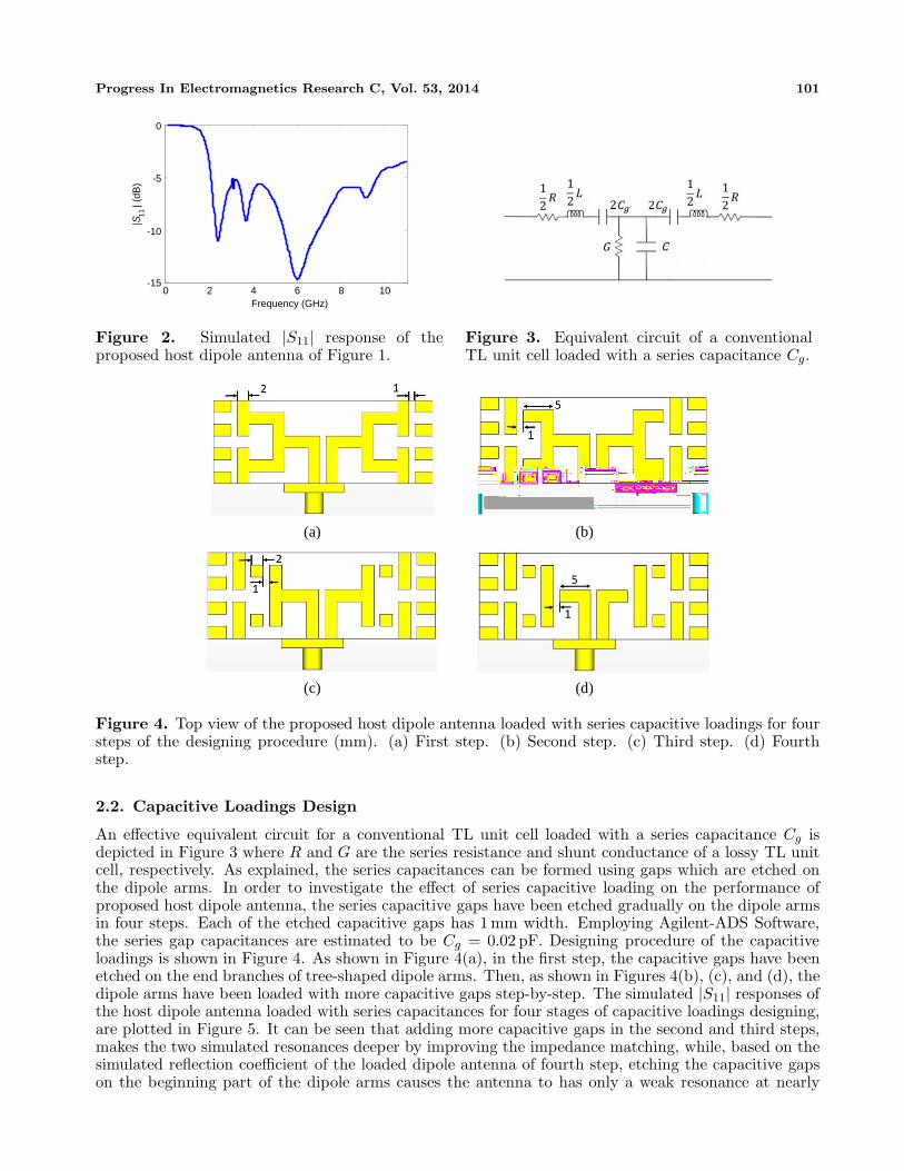
Configuration of the host dipole antenna with its geometrical parameters is shown in Figure 1. Theproposed antenna is designed on a FR-4 substrate with thickness of 1.6 mm, dielectric constant of 4.4,and loss tangent of 0.025. The thickness of used copper layers is 30µm. A 50-Ω SMA connector directlyfeeds the dipole arms by an edge-coupled coplanar strip (CPS) line. This type of feeding is used in [24]to feed a bow-tie planar dipole antenna. As shown in Figure 1(b), center conductor of SMA connectoris connected to the left CPS conductor and the outer surface of SMA connector is connected to theright CPS conductor. The CPS line is a balanced line which connects the unbalanced SMA connectorto the dipole arms. In fact, the CPS line works as a TL transformer. However, some low-magnitudecurrents flowing on the outer surface of the SMA connector, can be caused by the inherent imbalancebetween the balanced CPS line and the unbalanced SMA connector. These currents on the outside ofthe SMA connector surface, can cause the connector to slightly radiate. This may cause a distortion inthe radiation pattern of the dipole antenna. The simulated reflection coefficient of the proposed hostdipole antenna is plotted in Figure 2. All of the simulations and optimizations are performed usingCST Microwave Studio. It can be seen that the multiband resonant behavior is achieved by designingthe host dipole antenna based on a fractal-inspired geometry. As shown in Figure 2, the proposedhost dipole antenna has two resonances matched below −10 dB at 2.42 GHz, and 6 GHz with −10 dBbandwidths of 218 MHz, and 1.56 GHz, respectively.
(a) (b)
Figure 1. Geometry of the proposed host dipole antenna (mm). (a) Top view. (b) Configuration ofthe feeding part.
Progress In Electromagnetics Research C, Vol. 53, 2014 101
0 2 4 6 8 10Frequency (GHz)
|S11
| (dB
)
-15
-10
-5
0
Figure 2. Simulated |S11| response of theproposed host dipole antenna of Figure 1.
Figure 3. Equivalent circuit of a conventionalTL unit cell loaded with a series capacitance Cg.
(a) (b)
(c) (d)
Figure 4. Top view of the proposed host dipole antenna loaded with series capacitive loadings for foursteps of the designing procedure (mm). (a) First step. (b) Second step. (c) Third step. (d) Fourthstep.
2.2. Capacitive Loadings Design
An effective equivalent circuit for a conventional TL unit cell loaded with a series capacitance Cg isdepicted in Figure 3 where R and G are the series resistance and shunt conductance of a lossy TL unitcell, respectively. As explained, the series capacitances can be formed using gaps which are etched onthe dipole arms. In order to investigate the effect of series capacitive loading on the performance ofproposed host dipole antenna, the series capacitive gaps have been etched gradually on the dipole armsin four steps. Each of the etched capacitive gaps has 1 mm width. Employing Agilent-ADS Software,the series gap capacitances are estimated to be Cg = 0.02 pF. Designing procedure of the capacitiveloadings is shown in Figure 4. As shown in Figure 4(a), in the first step, the capacitive gaps have beenetched on the end branches of tree-shaped dipole arms. Then, as shown in Figures 4(b), (c), and (d), thedipole arms have been loaded with more capacitive gaps step-by-step. The simulated |S11| responses ofthe host dipole antenna loaded with series capacitances for four stages of capacitive loadings designing,are plotted in Figure 5. It can be seen that adding more capacitive gaps in the second and third steps,makes the two simulated resonances deeper by improving the impedance matching, while, based on thesimulated reflection coefficient of the loaded dipole antenna of fourth step, etching the capacitive gapson the beginning part of the dipole arms causes the antenna to has only a weak resonance at nearly

102 Jamilan, Tofigh, and Azarmanesh
0 2 4 6 8 10Frequency (GHz)
|S| (
dB)
First StepSecond StepThird StepFourth Step
-30
-25
-20
-15
-10
-5
0
11
Figure 5. Simulated |S11| responses of the proposed loaded dipole antennas of Figure 4 for four stepsof capacitive loadings designing.
1 2 3 4 5 6 7 8 9 10Frequency (GHz)
First StepSecond Step Third StepFourth Step
1 2 3 4 5 6 7 8 9 10Frequency (GHz)
First StepSecond Step Third StepFourth Step
0
50
100
150
Re
(Zin
)
-150
-100
-50
0
50
100
Im (
Z in)
(a) (b)
Figure 6. Simulated input impedances of the proposed loaded dipole antennas of Figure 4 for foursteps of capacitive loadings designing. (a) Real part. (b) Imaginary part.
(a) (b)
Figure 7. Geometry of the proposed loaded dipole antenna of Figure 4(c) for two different widths ofcapacitive gaps (mm). (a) 0.6 mm. (b) 0.2 mm.
5.2 GHz. Therefore, we can infer that the proposed loaded dipole antenna of Figure 4(c) shows betterimpedance matching compared to the loaded dipole antennas of Figures 4(a), (b), and (d).
The simulated results in Figure 6 show the real (resistance) and imaginary (reactance) parts of theinput impedances of the proposed antennas of Figure 4 for four steps of capacitive loadings designing.In order to have a very good impedance matching at a resonance with respect to a 50-Ω source, thereal and imaginary parts of the input impedance have to be 50-Ω and 0-Ω, respectively, for a samefrequency. Therefore, a very low return loss can be achieved when the real and imaginary parts ofthe input impedance satisfy the mentioned condition for the same frequency. It can be observed fromFigure 6 that for the third step of capacitive loadings designing, the real and imaginary parts of theinput impedance get closer to 50-Ω and 0-Ω, respectively, for the same frequencies at nearly 3.9 GHzand 6.7 GHz, resulting in a very low return loss. As depicted in Figure 7, the capacitive gaps width of

Progress In Electromagnetics Research C, Vol. 53, 2014 103
0 2 4 6 8 10Frequency (GHz)
|S11
| (dB
)
1 mm 0.6 mm0.2 mm
-30
-25
-20
-15
-10
-5
0
Figure 8. Simulated |S11| responses of the proposed loaded dipole antenna of Figure 4(c) for differentwidths of capacitive gaps.
(a) (b)
(c) (d)
Figure 9. Geometry of the proposed host dipole antenna loaded with three different designs of theparasitic element (mm). (a) Top view. (b) Bottom view of the first design. (c) Bottom view of thesecond design. (d) Bottom view of the third design.
the designed antenna of Figure 4(c) is decreased from 1 mm to 0.6 mm and 0.2 mm in order to revealits influence on the proposed antenna’s performance. The simulated reflection coefficients of antenna ofFigure 4(c) for different widths of the capacitive gaps are plotted in Figure 8. It can be observed thatby decreasing the width of etched gaps from 1 mm to 0.2 mm, the first and second resonance frequenciesslightly decrease.
2.3. Parasitic Element Design
Due to improve the proposed host antenna’s performance, the effect of a parasitic element on thebackside of the substrate is investigated in this section. In the first step of parasitic element designing,as shown in Figure 9(b), a straight thin strip is placed on the backside of the substrate as the parasiticelement. In next step, as shown in Figure 9(c), the proposed host dipole antenna is loaded with aparasitic element on the backside of the substrate which has a fractal-inspired geometry. This geometrycoincides with the tree-shaped fractal geometry of the dipole arms. The aim of this design is to increasethe desired influence of coupling between the dipole arms and the parasitic element on the resonantbehavior of proposed antenna. In the last step, twenty small rectangular patches have been added to theprevious designed parasitic element. Thin inductive strips join these small rectangular patches beneathone of the dipole arms, to other rectangular patches beneath the other dipole arm. The geometry of the

104 Jamilan, Tofigh, and Azarmanesh
0 2 4 6 8 10
|S11
| (dB
)
First DesignSecond DesignThird Design
-40
-35
-30
-25
-20
-15
-10
-5
0
Frequency (GHz)
Figure 10. Simulated |S11| responses of the proposed dipole antennas of Figure 9 loaded with threedifferent designs of the parasitic element.
(a) (b)
Figure 11. Geometry of the proposed dipole antenna loaded with both series capacitances and parasiticelement. (a) Top view of the loaded dipole antenna. (b) Bottom view of the loaded dipole antenna.
designed parasitic element with small patches is indicated in Figure 9(d). The simulated |S11| responsesof the proposed host dipole antenna loaded with different versions of the parasitic element shown inFigure 9, are plotted in Figure 10. It can be seen that when the host dipole antenna is loaded with afractal-inspired parasitic element, it is able to offer more resonances with better impedance matchingcompared to the host antenna loaded with a simple thin straight strip as the parasitic element. Inaddition, it can be observed that adding the small patches to the tree-shaped parasitic element, decreasesthe last two resonant bands frequencies and makes them deeper. Therefore, it can be concluded thatsmall patches has a positive effect on the proposed antenna’s performance.
2.4. Dipole Antenna Loaded with Both Series Capacitances and Parasitic Element
Based on the obtained results of above sections, it can be inferred that when the proposed host dipoleantenna is only loaded with series capacitances shown in Figure 4(c), it shows two deep resonances. Onthe other hand, when the proposed host dipole antenna is only loaded with the tree-shaped parasiticelement, it offers five resonances. It can be predicted that by loading the proposed host dipole antennawith both series capacitances and parasitic element, it can offer a multiband performance while allresonances are well-matched below −10 dB. The geometry of the proposed host dipole antenna loadedwith both series capacitances and parasitic element is shown in Figure 11. Regarding the obtainedresults of above sections, the capacitive loadings and parasitic element designs of Figures 4(c) and 9(d),respectively, are chosen to design the loaded dipole antenna of Figure 11. The simulated reflectioncoefficients of the proposed unloaded host dipole antenna of Figure 1 and loaded dipole antenna ofFigure 11 are plotted in Figure 12. It can be seen that the multiband behavior is achieved by loadingthe host fractal-inspired dipole antenna with series capacitive gaps and a parasitic element in order toform a loaded dipole antenna. The proposed loaded dipole antenna has more resonant frequency bandscompared to the host dipole antenna. Based on the simulated |S11| response of the proposed loadeddipole antenna of Figure 11, the resonances are centered at 1.52 GHz, 3.62 GHz, 4.6 GHz, 6.9 GHz,

Progress In Electromagnetics Research C, Vol. 53, 2014 105
0 2 4 6 8 10-40
-35
-30
-25
-20
-15
-10
-5
0
|S11
| (dB
)
Host AntennaLoaded Antenna
Frequency (GHz)
Figure 12. Simulated |S11| responses of the proposed host dipole antenna of Figure 1 and loaded dipoleantenna of Figure 11.
and 9.43 GHz and have −10 dB bandwidths of 50 MHz, 470 MHz, 170 MHz, 1.15 GHz, and 360 MHz,respectively. It can be observed that all simulated resonances of proposed loaded dipole antennaof Figure 11, are well-matched below −10 dB. We can infer that the employed loading improves theimpedance matching of the proposed dipole antenna with respect to the 50-Ω source. By comparing theobtained results of Figure 10 (for the third design of the parasitic element) and 12, it can be concludedthat adding the series capacitive loadings, while the antenna has been also loaded with the parasiticelement before, decreases the first resonance frequency from 2.4 GHz to 1.52 GHz and makes the secondand third resonances deeper.
The lowest resonant frequency of the proposed loaded dipole antenna of Figure 11 at 1.52 GHz,offers a large degree of miniaturization compared to the host dipole antenna of Figure 1. The loadeddipole antenna exhibits 0.9 GHz reduction of the lowest resonant frequency, compared to the host dipoleantenna which has the lowest resonant frequency of 2.42 GHz. The full size of the proposed loaded dipoleantenna is 37mm × 14mm × 1.6 mm, or 0.18λmm × 0.07λmm × 0.008λ with respect to the free spacewavelength λ at the lowest center resonant frequency of 1.52 GHz. Therefore, proposed antenna has anelectrically small dimensions in comparing with a conventional dipole antenna with 0.5λ length.
3. EXPERIMENTAL RESULTS AND DISCUSSIONS
Figure 13 shows the fabricated prototype of the proposed loaded dipole antenna of Figure 11. The |S11|response of the fabricated antenna is extracted by a vector network analyzer Agilent E8363C and shownin Figure 14. It can be seen that the experimental result and simulated result are in a good agreement
(a) (b)
Figure 13. Photographs of the fabricatedprototype of proposed loaded dipole antenna ofFigure 11. (a) Top view. (b) Bottom view.
0 2 4 6 8 10-40
-35
-30
-25
-20
-15
-10
-5
0
Frequency (GHz)
|S11
| (dB
)
SimulatedMeasured
Figure 14. Measured and simulated |S11|responses of the proposed loaded dipole antenna.

106 Jamilan, Tofigh, and Azarmanesh
-30
-20
-10 0 dB
30
210
60
240
90
270
120
300
150
330
180 0
-30
-20
-10
0 dB
30
210
60
240
90
270
120
300
150
330
180 0
-30
-20
-10
0 dB
30
210
60
240
90
270
120
300
150
330
180 0
-30
-20
-10
0 dB
30
210
60
240
90
270
120
300
150
330
180
-30
-20
-10
0 dB
30
210
60
240
90
270
120
300
150
330
180
(a) (b) (c)
(d) (e)
Figure 15. Measured radiation patterns of the fabricated loaded dipole antenna of Figure 13 at (a) 1.55,(b) 3.23, (c) 4.47, (d) 6.91, and (e) 9.76 GHz.
with each other. Some disagreements can be related to either the inaccuracies in the dimensions of thefabricated antenna’s elements produced during the fabrication process or measurement equipment orconnector or some interferences in measurement environment. The measured radiation patterns of thefabricated loaded dipole antenna of Figure 13 at its measured center resonant frequencies are plotted inFigure 15, where H-plane (yz-plane) and E-plane (xy-plane) radiation patterns at 1.55 GHz, 3.23 GHz,4.47 GHz, 6.91 GHz, and 9.76 GHz are shown. At the first resonant band, the proposed antenna exhibitsan excellent dipolar radiation pattern with a linear x-directed electric field polarization. However in thefirst resonant band, the proposed loaded dipole antenna has an x-directed linear E-field radiation withhigh-purity, but in the upper resonant bands, the y-directed currents along the vertical strips of dipolearms, have contribution to the cross-polarization.
Simulated peak gains of the proposed loaded dipole antenna of Figure 11, at center resonantfrequencies of 1.52 GHz, 3.62 GHz, 4.6 GHz, 6.9 GHz, and 9.43 GHz are 1.21 dBi, 2.24 dBi, 1.73 dBi,3.92 dBi, and 3.39 dBi, respectively, and simulated radiation efficiencies at the same resonant frequenciesare 86%, 90%, 72%, 78%, and 52%, respectively, while the measured peak gains of the fabricated loadeddipole antenna of Figure 13, at measured center resonant frequencies of 1.55 GHz, 3.23 GHz, 4.47 GHz,6.91 GHz, and 9.76 GHz are 1.1 dBi, 2.3 dBi, 1.9 dBi, 4.1 dBi, and 3.7 dBi, respectively, and measuredradiation efficiencies at same resonant frequencies are 83%, 90%, 70%, 74%, and 55%, respectively.The simulated current distribution on the backside of the substrate at the center resonant frequency of1.52 GHz is shown in Figure 16. As seen, there is a strong current flow on the thin strips. We can inferthat the parasitic element strongly acts as coupled resonator.
In order to investigate the effect of small rectangular patches of parasitic element on the performanceof the proposed loaded dipole antenna of Figure 11, the small patches from the parasitic element on thebackside of substrate are removed and the simulated |S11| response is shown in Figure 17. It can beseen that when the rectangular patches are removed, the |S11| response of the proposed loaded dipoleantenna of Figure 11 changes in all frequency bands except second resonance band. The disadvantageof removing patches is that the proposed antenna shows lower degree of miniaturization with respect tothe lowest resonance frequency. On the opposite side, the advantage is that another resonant frequencyis added at nearly 7.8 GHz. As shown in Figure 18, a sample of the proposed loaded dipole antenna

Progress In Electromagnetics Research C, Vol. 53, 2014 107
Figure 16. Simulated current distribution on the parasitic element at 1.52 GHz.
0 2 4 6 8 10-40
-35
-30
-25
-20
-15
-10
-5
0
Frequency (GHz)
|S11
| (dB
)
With PatchesWithout Patches
Figure 17. Simulated |S11| responses of theproposed loaded dipole antenna of Figure 11 withand without small patches in the parasitic elementstructure.
Figure 18. Bottom view photograph of thefabricated prototype of proposed loaded dipoleantenna of Figure 11 while the small patches areremoved from the parasitic element.
0 2 4 6 8 10 12-35
-30
-25
-20
-15
-10
-5
0
Frequency (GHz)
|S11
| (dB
)
SimulatedMeasured
Figure 19. Measured and simulated |S11|responses of the proposed loaded dipole antennaof Figure 11 while the small rectangular patchesare removed from the parasitic element.
0 2 4 6 8 10-40
-30
-20
-10
0
Frequency (GHz)
|S11
| (dB
)
0.1 mm0.3 mm0.5 mm
Figure 20. Simulated |S11| responses of theproposed loaded dipole antenna of Figure 11 fordifferent widths of the printed thin strips of theparasitic element on the backside of the substrate.
of Figure 11 with removed small rectangular patches from the parasitic element, is fabricated. Thereflection coefficient of the fabricated antenna of Figure 18 is measured and shown in Figure 19. Thereis a good agreement between the measured and simulated results.
Figure 20 shows the simulated reflection coefficients for a parametric study of the printed thinstrips width on the backside of the substrate of loaded dipole antenna of Figure 11, which join the smallrectangular patches together, while the other geometrical parameters are fixed. It can be observed thatthe width of the thin strips have an effective influence on the |S11| response of the proposed loadeddipole antenna of Figure 11. It should be noted that as the width is increased from 0.1 mm to 0.5 mm,the value of the lowest resonant frequency increases and therefore, the proposed loaded dipole antenna

108 Jamilan, Tofigh, and Azarmanesh
0 2 4 6 8 10-40
-30
-20
-10
0
Frequency (GHz)
|S11
| (dB
)
1 mm0.6 mm0.2 mm
Figure 21. Simulated |S11| responses of the proposed loaded dipole antenna of Figure 11 for differentwidths of the capacitive gaps.
offers a lower degree of miniaturization. Furthermore, by increasing the width of thin strips, centerfrequencies of other resonance bands also increase.
The amount of series capacitances are related to the width of etched gaps on the dipole arms. Thewidth of gaps are decreased from 1 mm to 0.2 mm in order to reveal the effect of series capacitive loadingson the resonant behavior of the proposed loaded dipole antenna of Figure 11, while the other geometricalparameters are fixed. Accordingly, the simulated reflection coefficients for different widths of the etchedgaps, are plotted in Figure 21. It can be observed that with increasing the width of etched gaps from0.2 mm to 1 mm, two resonance bands, between 6 GHz and 8GHz, merge and create a single resonanceband. In addition, we can infer that by altering the width of capacitive gaps, center frequencies of otherresonance bands can be changed accurately. Based on the obtained results of demonstrated parametricstudies, it is possible to control the resonance frequencies of the proposed loaded dipole antenna byaltering its geometrical parameters.
4. CONCLUSION
We have demonstrated the designing procedure of a novel low-profile multiband fractal-inspired dipoleantenna loaded with series capacitances and a parasitic element. The measured and simulated resultsreveal that when the designed host dipole antenna is loaded with series capacitances and a parasiticelement, it offers more resonant frequency bands with high degree of miniaturization. The designed seriescapacitive loadings and parasitic element are able to improve the impedance matching of proposed dipoleantenna. In addition, it is illustrated that by altering the various geometrical parameters of proposedantenna’s elements, accurate control of the antenna’s frequency bands can be obtained. Its compactsize, planar structure, multiband and high-efficiency performance make it amenable for novel wirelessapplications.
REFERENCES
1. Quan, X. L., R. L. Li, Y. H. Cui, and M. M. Tentzeris, “Analysis and design of a compact dual-banddirectional antenna,” IEEE Antennas Wireless Propag. Lett., Vol. 11, 547–550, May 2012.
2. Salonen, P., M. Keskilammi, and M. Kivikoski, “Single-feed dual-band planar inverted-F antennawith U-shaped slot,” IEEE Antennas Wireless Propag. Lett., Vol. 48, No. 8, 1262–1264, Aug. 2000.
3. Guo, Y. X., K. M. Luk, and K. F. Lee, “Dual-band slot-loaded short circuited patch antenna,”Electron. Lett., Vol. 36, No. 4, 289–290, Feb. 2000.
4. Wong, K. L., L. C. Chou, and C. M. Su, “Dual-band-plate antenna with a shorted parasitic elementfor laptop applications,” IEEE Trans. Antennas Propag., Vol. 53, No. 1, 539–544, Jan. 2005.
5. Suh, Y. H. and K. Chang, “Low cost microstrip-fed dual frequency printed dipole antenna forwireless communications,” Electron. Lett., Vol. 36, 1177–1179, Jul 2000.
Progress In Electromagnetics Research C, Vol. 53, 2014 109
6. Kuo, Y. L. and K. L. Wong, “Printed double-T monopole antenna for 2.4/5.2 GHz dual-bandWLAN operations,” IEEE Trans. Antennas Propag., Vol. 51, No. 9, 2187–2192, Sep. 2003.
7. Chou, L. C. and K. L. Wong, “Uni-planar dual-band monopole antenna for 2.4/5 GHz WLANoperation in the laptop computer,” IEEE Trans. Antennas Propag., Vol. 55, No. 12, 3739–3741,Dec. 2007.
8. Yang, H. Y. D. and Y. Y. Zhang, “A wideband miniaturized dipole antenna on a printed circuitboard,” Progress In Electromagnetics Research C, Vol. 10, 175–185, 2009.
9. Ku, C.-H. and H.-W. Liu, “Compact planar triple-band folded dipole antenna for WLAN/WiMAXapplications,” Progress In Electromagnetics Research C, Vol. 28, 1–13, 2012.
10. Li, X., L. Yang, S.-X. Gong, Y.-J. Yang, and J.-F. Liu, “A compact folded printed dipole antennafor UHF RFID reader,” Progress In Electromagnetics Research Letters, Vol. 6, 47–54, 2009.
11. Abu, M. and M. K. A. Rahim, “Triple-band printed dipole tag antenna for RFID,” Progress InElectromagnetics Research C, Vol. 9, 145–153, 2009.
12. Guo, Y. Y., X. M. Zhang, G. L. Ning, D. Zhao, X. W. Dai, and Q. Wu, “Miniaturized modifieddipoles antenna for WLAN applications,” Progress In Electromagnetics Research Letters, Vol. 24,139–147, 2011.
13. Li, X., L. Yang, S.-X. Gong, and Y.-J. Yang, “Dual-band and wideband design of a printed dipoleantenna integrated with dual-band balun,” Progress In Electromagnetics Research Letters, Vol. 6,165–174, 2009.
14. Zhang, R., G. Fu, Z.-Y. Zhang, and Q.-X. Wang, “A wideband planar dipole antenna with parasiticpatches,” Progress In Electromagnetics Research Letters, Vol. 20, 137–145, 2011.
15. Floc’h, J. M. and H. Rmili, “Design of multiband printed dipole antennas using parasitic elements,”Microw. Opt. Technol. Lett., Vol. 48, No. 8, 1639–1645, Aug. 2006.
16. Chang, K., H. Kim, and Y. J. Yoon, “A triple-band printed dipole antenna using parasiticelements,” Microw. Opt. Technol. Lett., Vol. 47, No. 3, 221–223, Nov. 2005.
17. Borja, A. L., “Dipole antenna with left-handed loading operating at a zero order mode,” ProgressIn Electromagnetics Research C, Vol. 19, 85–92, 2011.
18. Caloz, C. and T. Itoh, Electromagnetic Metamaterials, Transmission Line Theory and MicrowaveApplications, John Wiley & Sons, Inc., Hoboken, NJ, USA, 2006.
19. Werner, D. H. and S. Ganguly, “An overview of fractal antenna engineering research,”Ant. Prop. Mag., Vol. 45, No. 1, 38–57, 2003.
20. Kimouche, H. and H. Zemmour, “A compact fractal dipole antenna for 915 MHz and 2.4 GHz RFIDtag applications,” Progress In Electromagnetics Research Letters, Vol. 26, 105–114, 2011.
21. Puente, C., J. Claret, F. Sagues, J. Romeu, M. Q. Lopez-Salvans, and R. Pous, “Multibandproperties of a fractal tree antenna generated by electrochemical decomposition,” Electron. Lett.,Vol. 32, No. 25, 2298–2299, 1996.
22. Werner, D. H., A. R. Bretones, and B. R. Long, “Radiation characteristics of thin-wire ternaryfractal trees,” Electron. Lett., Vol. 35, No. 8, 609–610, 1996.
23. Petko, J. S. and D. H. Werner, “Miniature reconfigurable three-dimensional fractal tree antennas,”IEEE Trans. Antennas Propag., Vol. 52, No. 8, 1945–1956, Aug. 2004.
24. Li, D. and J.-F. Mao, “A Koch-like sided fractal bow-tie dipole antenna,” IEEE Trans. AntennasPropag., Vol. 60, No. 5, 2242–2251, May 2012.
Related Documents