A CMMB Mobile TV Tuner Frontend with Integrated RSSI for Dual-band Applications Hua Xu, Yin Shi, Member, IEEE, Fa Foster Dai*, Fellow, IEEE, Abstract - This paper presents a dual band CMMB mobile TV tuner frontend RFIC with integrated Received Signal Strength Indicator (RSSI). The tuner RFIC includes two sets of receiver front-ends for terrestrial and satellite applications. The front-ends further include LNAs with dual gain adjusting, variable gain amplifiers (VGAs), and a mixer with two gm cells plus a common LO switch cell. The built-in Automatic Gain Control (AGC) loop meets wide dynamic range requirement of the mobile TV tuner. The tuner is integrated in a O.5um SiGe BiCMOS technology and consumes 16mA current from 2.8V supply. The RSSI is fully integrated with only two off-chip capacitors for low pass filtering. The tuner frontend RFIC achieves 45dB of maximum gain, 70dB gain control range, and an IIP3 higher than 18 dBm in minimum gain mode. Index Terms - Automatic Gain Control, CMMB, direct conversion, LNA, mixer, VGA, RSSI. I. INTRODUCTION The Chinese Mobile Multimedia Broadcasting (CMMB) is the emerging mobile TV standard based on a mixed satellite and terrestrial wireless broadcasting system designed to provide audio, video and data services for handheld receivers. CMMB utilizes two S-band satellites to cover the digital video broadcasting (DVB) over the wide area. In the populated metropolitan areas, CMMB utilizes the cellular base stations to enhance the digital video transmission in order to allow DVB reception with low-cost terminals. The service operates in both S-band (2635---2660MHz) and V-band (470---860MHz). An important specification for mobile reception is the system sensitivity. The noise figure (NF) of the receiver directly affects the signal demodulation with a given bit-error rate (BER). On the other hand, adjacent channels could be broadcast at significantly higher power. Therefore, linearity performance (1IP3) needs to support the desired channel reception while dealing with interferers at adjacent channels up to 50dB higher. The authors are with Suzhou-CAS Semiconductors Integrated Technology Co., Ltd., SuZhou, China (e-mail: [email protected]). * Fa Foster Dai is with the Electrical and Computer Engineering Department, Auburn University, Auburn, AL 36849-5201, USA (e-mail: fosterdai@ auburn.edu). 978-1-4244-3870-9/09/$25.00 ©2009 IEEE On chip I LNA VGA I SBAND_IN I BBOUT UBANDJN Fig. 1 Block diagram of the proposed CMMB tuner front-end RFIC. Additionally, low-cost and low power consumption is critical for mobile applications [1]-[3]. With these requirements, Zero-IF or Low-IF is more suitable for tuners for handheld devices. This work reports the design and implementation of a dual-band direct-conversion Zero-IF BiCMOS SiGe mobile tuner front-end RFIC. RF-VGAs with large dynamic range are included to achieve high IIP3 performance. A simplified block diagram of the proposed CMMB tuner receiver is shown in Fig. 1. Next, we will present the circuit design and implementation of the CMMB tuner front-end RFIC in details. The experimental results and conclusion are given in Section III and Section IV respectively. II. CIRCUITS IMENPLETATION As illustrated in Fig.1, the tuner receiver front-end includes two single-ended low-noise amplifiers (LNAs) with two gain modes (high gain/low gain, HG/LG). The LNA for the S-band reception uses on-chip inductor degeneration and LC tank load for realizing narrow-band match and low NF. Another LNA for the If-band reception employs a resistor-capacitor shunt feedback and resistive load for realizing wide-band match and transfer function. Both of the LNAs attain NF lower than 2dB in high gain mode and IIP3 of more than 20dBm in low gain mode. Following the LNAs, continuously tuned RF-VGAs with 50dB gain control range for both bands are implemented to meet the high linearity requirement. A resistive degenerated double-balanced Gilbert cell mixer for down conversion with different input Gm cells to amplify the signals 351 Authorized licensed use limited to: Auburn University. Downloaded on February 1, 2010 at 20:31 from IEEE Xplore. Restrictions apply.

Welcome message from author
This document is posted to help you gain knowledge. Please leave a comment to let me know what you think about it! Share it to your friends and learn new things together.
Transcript
A CMMB Mobile TV Tuner Frontend withIntegrated RSSI for Dual-band Applications
Hua Xu, Yin Shi, Member, IEEE, Fa Foster Dai*, Fellow, IEEE,
Abstract - This paper presents a dual band CMMBmobile TV tuner frontend RFIC with integratedReceived Signal Strength Indicator (RSSI). The tunerRFIC includes two sets of receiver front-ends forterrestrial and satellite applications. The front-endsfurther include LNAs with dual gain adjusting, variablegain amplifiers (VGAs), and a mixer with two gm cellsplus a common LO switch cell. The built-in AutomaticGain Control (AGC) loop meets wide dynamic rangerequirement of the mobile TV tuner. The tuner isintegrated in a O.5um SiGe BiCMOS technology andconsumes 16mA current from 2.8V supply. The RSSI isfully integrated with only two off-chip capacitors forlow pass filtering. The tuner frontend RFIC achieves45dB of maximum gain, 70dB gain control range, andan IIP3 higher than 18 dBm in minimum gain mode.
Index Terms - Automatic Gain Control, CMMB,direct conversion, LNA, mixer, VGA, RSSI.
I. INTRODUCTION
The Chinese Mobile Multimedia Broadcasting(CMMB) is the emerging mobile TV standard based ona mixed satellite and terrestrial wireless broadcastingsystem designed to provide audio, video and dataservices for handheld receivers. CMMB utilizes twoS-band satellites to cover the digital video broadcasting(DVB) over the wide area. In the populatedmetropolitan areas, CMMB utilizes the cellular basestations to enhance the digital video transmission inorder to allow DVB reception with low-cost terminals.The service operates in both S-band (2635---2660MHz)and V-band (470---860MHz).
An important specification for mobile reception isthe system sensitivity. The noise figure (NF) of thereceiver directly affects the signal demodulation with agiven bit-error rate (BER). On the other hand, adjacentchannels could be broadcast at significantly higherpower. Therefore, linearity performance (1IP3) needs tosupport the desired channel reception while dealingwith interferers at adjacent channels up to 50dB higher.
The authors are with Suzhou-CAS Semiconductors IntegratedTechnology Co., Ltd., SuZhou, China (e-mail: [email protected]).
* Fa Foster Dai is with the Electrical and Computer EngineeringDepartment, Auburn University, Auburn, AL 36849-5201, USA(e-mail: fosterdai@ auburn.edu).
978-1-4244-3870-9/09/$25.00 ©2009 IEEE
On chip
r---------~...,I LNA VGA I
SBAND_IN IBBOUT
UBANDJN
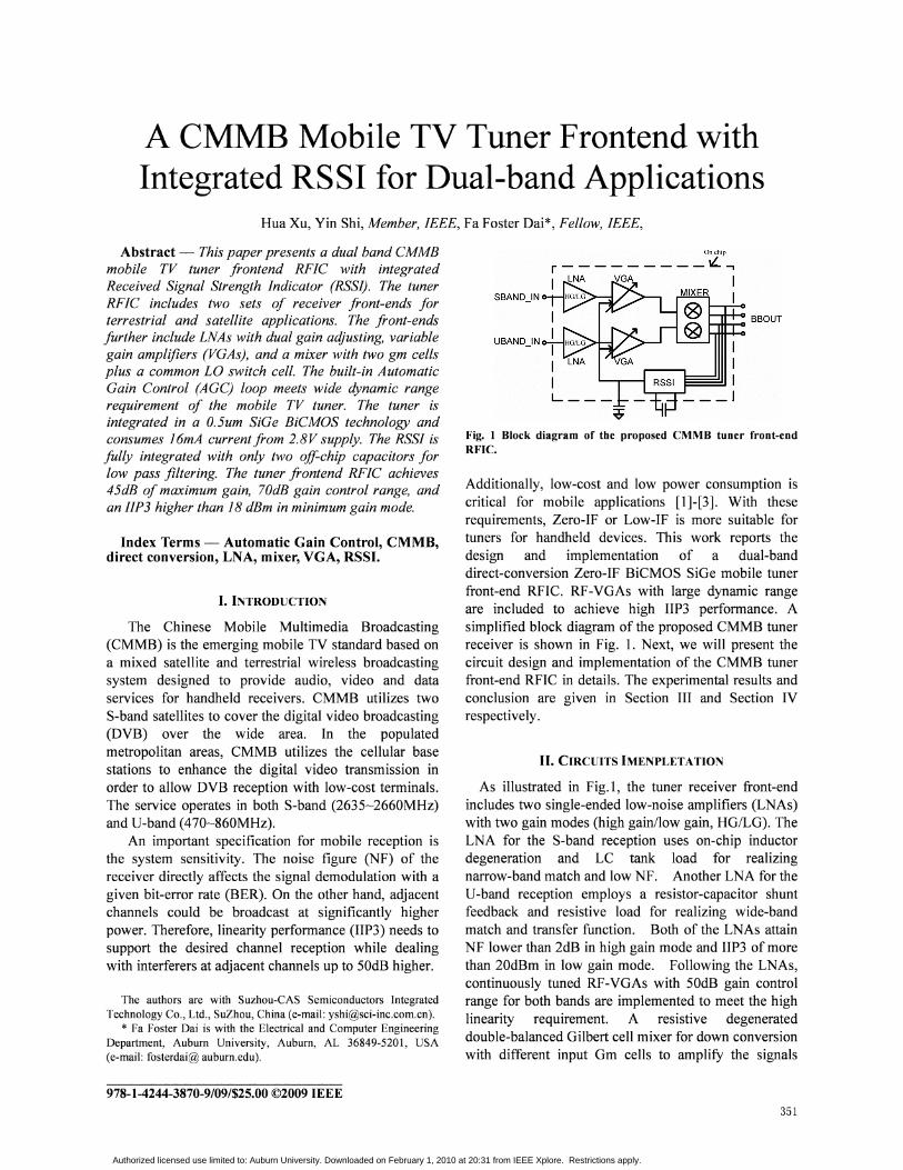
Fig. 1 Block diagram of the proposed CMMB tuner front-endRFIC.
Additionally, low-cost and low power consumption iscritical for mobile applications [1]-[3]. With theserequirements, Zero-IF or Low-IF is more suitable fortuners for handheld devices. This work reports thedesign and implementation of a dual-banddirect-conversion Zero-IF BiCMOS SiGe mobile tunerfront-end RFIC. RF-VGAs with large dynamic rangeare included to achieve high IIP3 performance. Asimplified block diagram of the proposed CMMB tunerreceiver is shown in Fig. 1. Next, we will present thecircuit design and implementation of the CMMB tunerfront-end RFIC in details. The experimental results andconclusion are given in Section III and Section IVrespectively.
II. CIRCUITS IMENPLETATION
As illustrated in Fig.1, the tuner receiver front-endincludes two single-ended low-noise amplifiers (LNAs)with two gain modes (high gain/low gain, HG/LG). TheLNA for the S-band reception uses on-chip inductordegeneration and LC tank load for realizingnarrow-band match and low NF. Another LNA for theIf-band reception employs a resistor-capacitor shuntfeedback and resistive load for realizing wide-bandmatch and transfer function. Both of the LNAs attainNF lower than 2dB in high gain mode and IIP3 of morethan 20dBm in low gain mode. Following the LNAs,continuously tuned RF-VGAs with 50dB gain controlrange for both bands are implemented to meet the highlinearity requirement. A resistive degenerateddouble-balanced Gilbert cell mixer for down conversionwith different input Gm cells to amplify the signals
351
Authorized licensed use limited to: Auburn University. Downloaded on February 1, 2010 at 20:31 from IEEE Xplore. Restrictions apply.
Vb1
receiver must be able to handle signals with a wideinput dynamic range from -100dBm to OdBm, widegain tuning at the front-end is thus necessary to meetthe noise and linearity requirements over the entireinput range. As shown in Fig. 3, the core of theRF-VGA circuit consists of a three-stage capacitiveattenuator with 14dB per stage attenuation and fouramplifiers which smoothly switch outputs from theladder attenuator. The VGA architecture has its originin the VGA using resistive attenuator proposed by [4].The modification with capacitive attenuator is reportedin [5]-[7]. By distributing a fixed amount of current tothe input transistor collector with an appropriate ratiocorresponding to the control voltage, the gain of theVGA can be tuned continuously.
C. Received Signal Strength Indicator (RSSI)
Fig. 4 Proposed RSSI architecture.
A received signal strength indicator (RSSI) isemployed to sense the received signal strength. In thisdesign, it is used to adjust the gains of the RF front-end.The RSSI is generally realized in logarithmic formatbecause the wide dynamic variation of the receivedsignal can be represented within a limited indicationrange. Successive-detection architecture is adopted forrealizing the logarithmic amplifier. It is essentiallycomposed of several full-wave rectifiers and a low-passfilter, which are in combination with the existinglimiting amplifier circuits. Thus successive-detection ispower efficient [8]-[11].
In Fig. 4, the topology of the adopted RSSI isprovided. It detects the output signal amplitude of thedown-conversion mixer and produces a detected DClevel to control the gain of both RF-VGAs. As shown inFig. 4, each power detector detects the signal from theoutput of each limiting amplifier and generates a decurrent after filtering. All of the currents are added atone port of the load resistor and capacitor. Anotherport of the load resistor and capacitor is connected toground.On the other hand, due to the large gain of the chain oflimiting amplifiers, a de-offset cancellation circuit isessential since any offset caused by device mismatchmay degrade small input signal. The input offsetvoltage of this negative feedback cancellation, as shown
The RF variable gain amplifier (RF-VGA) followingthe LNA, is used to attain power gain and achieve widetunable gain range for the front-end. Since the CMMB
Fig. 3 RFVGA schematic diagram.
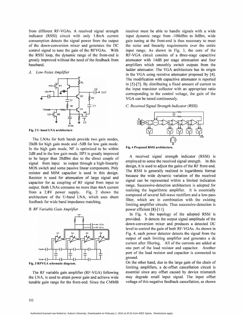
The LNAs for both bands provide two gain modes,20dB for high gain mode and -5dB for low gain mode.In the high gain mode, NF is optimized to be within2dB and in the low gain mode, IIP3 is greatly improvedto be larger than 20dBm due to the direct couple ofsignal from input to output through a high-linearityMOS switch and some passive linear components. Polyresistor and MIM capacitor is used in this design.Resistor is used for attenuation of large signal andcapacitor for ac coupling of RF signal from input tooutput. Both LNAs consume no more than 4mA currentfrom a 2.8V power supply. Fig. 2 shows thearchitecture of the If-band LNA, which uses shuntfeedback for wide band impedance matching.
B. RF Variable Gain Amplifier
RFIN
Fig. 2 V-band LNA architecture
Vbiaso---.--'VV'v.........--t
from different RF-VGAs. A received signal strengthindicator (RSSI) circuit with only 1.8mA currentconsumption detects the signal power from the outputof the down-conversion mixer and generates the DCcontrol signal to tune the gain of the RFVGAs. Withthe RSSI loop, the dynamic range of the front-end isgreatly improved without the need of the feedback frombaseband.
A. Low-Noise Amplifier
352
Authorized licensed use limited to: Auburn University. Downloaded on February 1, 2010 at 20:31 from IEEE Xplore. Restrictions apply.
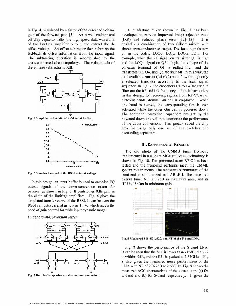
Fig. 7 Double-Gm quadrature down-conversion mixer.
Fig. 8 Measured SII, S21, S22, and NF of the U-band LNA.
III. EXPERIMENTAL RESULTS
The die photo of the CMMB tuner front-endimplemented in a 0.35um SiGe BiCMOS technology isshown in Fig. 10. The presented tuner RFIC has beentested and the front-end performs meet the CMMBsystem requirements. The measured performance of thefront-end is summarized in TABLE I. The measuredoverall tuner NF is 2.2dB in maximum gain, and itsIIP3 is 18dBm in minimum gain.
Fig. 8 shows the performance of the S-band LNA.It can be seen that the S11 is lower than -15dB, the S22is within -9dB, and the S21 is peaked at 2.68GHz. Fig.8 also gives the measured noise performance of theLNA with NF of2.077dB at 2.68GHz. Fig. 9 shows themeasured AGC characteristic of the closed loop, (a) forIf-band and (b) for S-band respectively. It gives the
A quadrature mixer shown in Fig. 7 has beendeveloped to provide improved image rejection ratio(IRR) and reduced phase error [12]-[13]. It isbasically a combination of two Gilbert mixers withshared transconductance stages. The local signals tumon in the order: LOQp, LOlp, LOQn, LOIn. Forexample, when the RF signal on transistor Ql is highand the LOQp signal on Q7 is high, the voltage of thecollector terminal of Q1 is pulled high and thetransistors Q3, Q4, and Q8 are shut off. In this way, thetotal available current (Icl +lc2) must flow through onlya selected transistor according to the local signalsequence. In Fig. 7, the capacitors C1 to C4 are used tofilter out the RF and LO frequency and their harmonics.In this design, for receiving signals from RF-VGAs ofdifferent bands, double Gm cell is employed. Whenone band is started, the corresponding Gm is thenactivated while the other Gm cell is powered down.The additional parasitical capacitors brought by thepowered down one will not deteriorate the performanceof the down conversion. This greatly saved the chiparea for using only one set of LO switches anddecoupling capacitors.
LOOp
100
'"----+---0 LOan
I-.- RSSIOUT vs INPUT I
10
INput Voltage ( mV)
2.6
LOI
LOlno----+----'
Fig. 6 Simulated output of the RSSI vs input voltage.
Fig. 5 Simplified schematic of RSSI input buffer.
In this design, an input buffer is used to combine I/Qoutput signals of the down-conversion mixer forbalance, as shown in Fig. 5. It contributes OdB gain inthe chain of the limiting amplifiers. Fig. 6 gives thesimulated transfer curve of the RSSI. It can be seen theRSSI can detect signal as low as ImV, which meets theneed of gain control for wide input dynamic range.
D. I/Q Down-Conversion Mixer
in Fig. 4, is reduced by a factor of the cascaded voltagegain of the forward path [5]. An n-well resistor andoff-chip capacitor filter the high-speed data waveformof the limiting amplifier output, and extract the dcoffset voltage. An offset subtractor then subtracts thefed-back dc offset information from the input signal.The subtracting operation is accomplished by thecross-connected circuit topology. The voltage gain ofthe voltage subtractor is OdB.
::.~2.0 ""- <,
~1.8 <;'iii 1.6 ~
$1.4 "'~1.2 "<,1.0
353
Authorized licensed use limited to: Auburn University. Downloaded on February 1, 2010 at 20:31 from IEEE Xplore. Restrictions apply.
IV. CONCLUSIONS
A CMMB mobile TV tuner frontend with integratedRSSI for dual-band applications has been implementedin a O.35um BiCMOS SiGe technology. Themeasurement results show that the front-end tunerRFIC is compliant with the newly released ChineseCMMB mobile TV requirements with a state of the artgain control range of 65dB and overall NF of 2.2dB.Low power consumption of 48mW is achieved, whichis suitable for the CMMB receiver integrated in amobile environment.
voltage output Vrssi of the RSSI circuit and RF-VGAgain versus the input power variation. In the figure,Vrssi_HG and Vrssi_LG represent RSSI output voltagewhen the LNA is settled high gain and low gain,respectively. GAIN HG or GAIN_LG representRF-VGA gain when LNA gain is settled high or low. Itcan be seen, for If-band reception, when input changesfrom -100dBm to -40dBm, the gain of the RF-VGA canbe adjusted for about 35dB. It greatly improved theinput linearity. On the other hand, from the figure, wecan see that the AGC begins to work when the inputpower is larger than -85dBm for U-band and -75dBmfor S-band. For If-band reception, when input power is-5dBm, the gain of the RF-VGA can be tuned to be-20dB.
Current consumption lower than 17mA
REFERENCES
TABLE I
SUMMARY OFMEASURED TUNER FRONT-END PERFORMANCE
[1] M. Dawkins, et aI., "A Sing-Chip Tuner for DVB-T.", IEEE JSolid-State Circuits, vol. 38, NO.8, pp. 1307-1317, August2003.
[2] I. Mehr, et a/., "A Dual-Conversion Tuner for Multi-StandardTerrestrial and Cable Reception" 2005 Symposium on VLSICircuits Digest ofTechnical Papers.
[3] S. Amiot, et aI., "A Low Power DVB-T/H Zero-IF Tuner ICDesign in 0.25 urn BiCMOS Technology for Mobile TVReception." IEEE TRANSACTIONS ON BROADCASTING, vol.53, NO.1, March 2007.
[4] B. Gilbert, "A low-Noise Wideband Variable-Gain AmplifierUsing an Interpolated Ladder Attenuator," ISSCC Dig. Tech.Papers, pp. 280-281, Feb. 1991.
[5] S.Azuma et a/., "A Digital Terrestrial Television (ISDB- T)Tuner for Mobile Applications," in IEEE ISSCC 2004 Dig. Tech.Papers, pp. 278-279.
[6] K. Iizuka et aI., "A 184 mW Fully Integrated DVB-H TunerWith a Linearized Variable Gain LNA and Quadrature MixersUsing Cross-Coupled Transconductor," IEEE J Solid-StateCircuits, vol. 42, NO.4, pp. 862-871, Apr. 2007
[7] H. Kawamura et aI., "A 184mW Fully Integrated DVB-H TunerChip with Distortion Compensated Variable Gain LNA," VLSIDig. Tech. Papers, 2006.
[8] P.Huang et al., "A 2-V 10.7-MHz CMOS LimitingAmplifier/RSSI", IEEE J Solid-State Circuits, vol. 35, NO. 10,pp. 1474-1480, Oct. 2000
[9] W. L. Barber and E. R. Brown, "A true logarithmic amplifier forradar IF applications," IEEE J Solid-State Circuits, vol SC-15,pp. 291-295, June 1980.
[10] C. Wu and H. Tsao, "A 110-MHz 84-dB CMOSProgrammable Gain Amplifier With Integrated RSSIFunction." IEEE J Solid-State Circuits, vol. 40, NO.6, pp.1249-1257, June 2005.
[11] T. W. Kim and B. Kim, "A 13-dB IIP3 Improved Low-PowerCMOS RF Programmable Gain Amplifier Using DifferentialCircuit Transconductance Linearization for Various TerrestrialMobile D-TV Applications." IEEE J Solid-State Circuits, vol.41, NO.4, pp. 945-953, April 2006.
[12] J. Harvey and R. Harjani, "Analysis and design of an integratedquadrature mixer with improved noise, gain, and imagerejection," in Proc. IEEE Int. Symp. Circuits and Systems, May2001, vol. IV, pp. 786-789.
[13] K. Taniguchi et aI., "A study on a GPS dual-band image-rejectmixer." IEICE, Tech. Rep. IEICE ICD2003-100 (2003-09).
--+-GAIN_HG
GAIN_LG
-+-Vrssi_HG
1 ~ ---Vrssi LG
o L") 0 U) 0 L<") a 1O"':t' (") M C'1 N ............. I
~
~ 10
Chip die micrograph.
(a) U-band
Fig. to
(b) S-band INPUTPOWER ( dB m)
Fig. 9 Measured Vrssi and RF-VGA gain of the closed loop.
Parameter ValueNoise figure~maximum gain 2.2dBmaximum gain of front-end 40dBIIP3@min gain 18dBmLNA gain tuning step 25dBRFVGA control range 41dBSupply voltage 2.8V
354
Authorized licensed use limited to: Auburn University. Downloaded on February 1, 2010 at 20:31 from IEEE Xplore. Restrictions apply.
Related Documents


![Rapport simplifié d'activité 2019 vf[1] - CMMB](https://static.cupdf.com/doc/110x72/62aae8239ea9c06c284943dd/rapport-simplifi-dactivit-2019-vf1-cmmb.jpg)