A CLUSTERING BASED AREA I/O PLANNING FOR FLIP-CHIP TECHNOLOGY Janet Wang Kishore Kumar Muchherla Jai Ganesh Kumar Department of Electrical Computer Engineering University of ARizona at TUCSON [email protected], {kishorem, jgk}@email.arizona.edu ABSTRACT The complexity of nanometer SoC design requires the co- design and development of circuit design and packaging technology to enable a successful 'total integrated solution'. In this paper we introduce a new area I/O algorithm for the recent flip-chip packaging technology. The algorithm combines a clustering technique with area I/O planning algorithm to avoid iterations during “placement and area I/O pad assignment”. Experiment results show that the total interconnect length (including both on-chip and off-chip parts) and delay are reduced by 10-15% comparing with traditional algorithms. 1. INTRODUCTION As the semiconductor industry drives into nanometer silicon technologies, the race to keep up with Moore's Law has hit some stumbling blocks. Since the introduction of SoC design methodologies in the mid '90's, silicon and packaging technologies have been pushed hard to support higher performance, lower power, finer geometries and denser I/O solutions. With SoC design methodology, complete systems have been integrated into single chip solutions. This high level of integration has created new demands for packaging technology. IC packaging technologies with peripheral I/O pads have several short comings. The complexity of the system and the calculated Rent parameters suggest that ICs require asymptotically more pads than the die perimeter can provide [9]. Peripheral I/O pads also constrain clock/power distribution, and their inherently large parasitics cause coupling and power issues for off-chip signaling. Moreover I/O counts have increased from the low hundreds in the early '90's to a few thousands today. For some high end microprocessors the electrical performance and I/O densities can not be easily realized with wire bonding based solutions. Given these concerns, the area I/O regime (flip chip) is predicted to eventually dominate IC implementation methodology. It offers improved pad count and reliability, reduced noise coupling, and cost savings as the technology matures. Flip chip packaging technology utilizes very small solder spheres, known as solder bumps. These bumps are part of the silicon chip. The silicon chip with bumps is mounted on the package substrate, similar in operation to a surface mount board assembly process. Flip chip technology provides 5-10 times more I/Os than the traditional method of restricting the I/Os to the periphery [1] [7]. Moreover, flip chip interconnect offers lower I/O inductance, better power / ground distribution, and flexibility to connect directly from the package to anywhere on the die. To develop a successful SoC design with flip chip packaging technology, the package must be part of the design cycle from the very beginning. Unfortunately, existing CAD algorithms are for peripheral packaging technologies [2]. In addition, most of them separate the package design from the design cycle and treat the packaging technology as a 'plug and play' component for the silicon chip design. The Cascade Design Automation recently reported a version of the CAD tool for designing area-array ICs [3]. This tool consists of an area-pad power analyzer, an area pad floor planner and an area pad router. The paper presented by Kiamilev et. al. [4] demonstrated three methods of designing an intrinsic area array IC. The problem with their approach is that the placement and routing of the area pads must be done manually and it has low packing density. The paper by Tan et. al [1] discusses about an area array pad router that automates the placement and routing of the area-array pads on the IC. The problem with this approach is that this is a post processing tool that can be used after initial IC layout generation. It does not take into consideration the packaging and off chip pad placement constraints as well as the “illegal regions “in the IC. The paper by Caldwell et. al [8] deals with an empirical study on the impact of area array I/O on placement. The results show that the use of area array I/O leads to shorter wire lengths and better placement when compared to peripheral I/O placement. In this paper, we propose a clustering based area I/O pad planning algorithm for flip chip packaging technology. Based on our algorithm we have developed a prototype tool called APT (A rea I/O P lanning T ool). Our algorithm has two phases: clustering and planning. In the clustering phase, we set the initial cluster area as the pad pitch area (area enclosed by four I/O pads on the die) so that after the clustering procedure, the resulting clusters will have predefined area with bumps surrounding them. In the planning phase, we plan the core logic and the I/O clusters simultaneously so that interconnects both off chip and on chip are minimized, considering predefined area I/O pads in the illegal regions (pre-assigned to power and ground lines). The algorithm is non iterative and integrates physical design issues along with packaging constraints . It provides a “total integrated solution” and can be used for SoC as well as SIP design methodologies. Experiment results show that the total interconnect length (including both on-chip and off-chip parts) is reduced by 10-15 %, compared with the traditional iterative algorithms where the I/O assignment was based on a predefined placement. It also achieves a speed up of 10-15X over the traditional iterative algorithms. The rest of the paper is organized as follows. Section 2 presents the problem formulation and preliminaries. Section 3 gives a detailed description of the APT algorithm. Section 4 presents the experimental results conducted on large test circuits and Section 5 concludes the paper with insight into future work. 2. PROBLEM FORMULATION 0-7695-2093-6/04 $20.00 2004 IEEE

Welcome message from author
This document is posted to help you gain knowledge. Please leave a comment to let me know what you think about it! Share it to your friends and learn new things together.
Transcript

A CLUSTERING BASED AREA I/O PLANNING FOR FLIP-CHIP TECHNOLOGY
Janet Wang Kishore Kumar Muchherla Jai Ganesh KumarDepartment of Electrical Computer Engineering
University of ARizona at [email protected], {kishorem, jgk}@email.arizona.edu
ABSTRACTThe complexity of nanometer SoC design requires the co-design and development of circuit design and packaging technology to enable a successful 'total integrated solution'. In this paper we introduce a new area I/O algorithm for the recent flip-chip packaging technology. The algorithm combines a clustering technique with area I/O planning algorithm to avoid iterations during “placement and area I/O pad assignment”. Experiment results show that the total interconnect length (including both on-chip and off-chip parts) and delay are reduced by 10-15% comparing with traditional algorithms.
1. INTRODUCTIONAs the semiconductor industry drives into nanometer silicon technologies, the race to keep up with Moore's Law has hit some stumbling blocks. Since the introduction of SoC design methodologies in the mid '90's, silicon and packaging technologies have been pushed hard to support higher performance, lower power, finer geometries and denser I/O solutions. With SoC design methodology, complete systems have been integrated into single chip solutions. This high level of integration has created new demands for packaging technology.
IC packaging technologies with peripheral I/O pads have several short comings. The complexity of the system and the calculated Rent parameters suggest that ICs require asymptotically more pads than the die perimeter can provide [9]. Peripheral I/O pads also constrain clock/power distribution,and their inherently large parasitics cause coupling and power issues for off-chip signaling. Moreover I/O counts have increased from the low hundreds in the early '90's to a few thousands today. For some high end microprocessors the electrical performance and I/O densities can not be easily realized with wire bonding based solutions. Given these concerns, the area I/O regime (flip chip) is predicted to eventually dominate IC implementation methodology. It offers improved pad count and reliability, reduced noise coupling, and cost savings as the technology matures.
Flip chip packaging technology utilizes very small solder spheres, known as solder bumps. These bumps are part of the silicon chip. The silicon chip with bumps is mounted on the package substrate, similar in operation to a surface mount board assembly process. Flip chip technology provides 5-10 times more I/Os than the traditional method of restricting the I/Os to the periphery [1] [7]. Moreover, flip chip interconnect offers lower I/O inductance, better power / ground distribution, and flexibility to connect directly from the package to anywhere on the die. To develop a successful SoC design with flip chip packaging technology, the package must be part of the design cycle from the very beginning. Unfortunately, existing CAD
algorithms are for peripheral packaging technologies [2]. In addition, most of them separate the package design from thedesign cycle and treat the packaging technology as a 'plug and play' component for the silicon chip design.
The Cascade Design Automation recently reported a version of the CAD tool for designing area-array ICs [3]. This tool consists of an area-pad power analyzer, an area pad floor planner and an area pad router. The paper presented by Kiamilev et. al. [4] demonstrated three methods of designing an intrinsic area array IC. The problem with their approach is thatthe placement and routing of the area pads must be done manually and it has low packing density. The paper by Tan et. al [1] discusses about an area array pad router that automates the placement and routing of the area-array pads on the IC. The problem with this approach is that this is a post processing tool that can be used after initial IC layout generation. It does not take into consideration the packaging and off chip pad placement constraints as well as the “illegal regions “in the IC.The paper by Caldwell et. al [8] deals with an empirical study on the impact of area array I/O on placement. The results show that the use of area array I/O leads to shorter wire lengths and better placement when compared to peripheral I/O placement.
In this paper, we propose a clustering based area I/O pad planning algorithm for flip chip packaging technology. Based on our algorithm we have developed a prototype tool called APT (Area I/O Planning Tool). Our algorithm has two phases: clustering and planning. In the clustering phase, we set the initial cluster area as the pad pitch area (area enclosed by four I/O pads on the die) so that after the clustering procedure, the resulting clusters will have predefined area with bumps surrounding them. In the planning phase, we plan the core logic and the I/O clusters simultaneously so that interconnects both off chip and on chip are minimized, considering predefined area I/O pads in the illegal regions (pre-assigned to power and ground lines).
The algorithm is non iterative and integrates physical design issues along with packaging constraints. It provides a “total integrated solution” and can be used for SoC as well as SIP design methodologies. Experiment results show that the total interconnect length (including both on-chip and off-chip parts) is reduced by 10-15 %, compared with the traditional iterative algorithms where the I/O assignment was based on a predefined placement. It also achieves a speed up of 10-15Xover the traditional iterative algorithms. The rest of the paper is organized as follows. Section 2 presents the problem formulation and preliminaries. Section 3 gives a detailed description of the APT algorithm. Section 4 presents the experimental results conducted on large test circuits and Section 5 concludes the paper with insight into future work.
2. PROBLEM FORMULATION
0-7695-2093-6/04 $20.00 2004 IEEE

Figure 1 shows the basic structure of a flip chip (FC) package. Flip chip packaging technology utilizes very small solder spheres that are 70µm to 100 µm high and 80 µm to 125 µm wide. The position of the solder bumps are predefined and are arranged in the form of a matrix. The silicon chip with bumps is mounted on the package substrate where a predefined array of substrate pads “touch” these bumps to establish connection.
The inputs to our algorithm are a VHDL/ Verilog netlist (comprises of primary inputs, outputs, IP blocks, and gates), list of IP blocks and a technology file (consists of pad pitch size and matrix of solder bumps with illegal I/O pad regions). The core objective is to place and route these components (taking into account the ‘illegal regions’) along with off chip and on chip I/Opads so that we get an optimized total wiring length (includes both on-chip and off-chip interconnects) and delay.
As the feature size continues to shrink with the advent of SoC and other design methodologies, the circuit size becomes larger and increasingly difficult to handle. By pre-processing the netlist and creating a clustered netlist, the problem size becomes more manageable. The other reason for clustering is that in a design with widely varying cell sizes, the clustering step is used to create clusters of roughly equivalent size therebyenabling the use of cell-oriented algorithms on the clustered netlist. In the clustering phase, we set the initial cluster area as the pad pitch area (area between four I/O pads on the die) so that after the clustering procedure, the resulting clusters will have predefined area (in terms of pad pitch) with I/O pad connections (Solder bumps) adjoining them.
In the planning phase, we use a heuristic algorithm to plan the core logic and the I/O clusters simultaneously so that interconnects, both off chip and on chip are minimized, considering predefined illegal regions (pre-assigned to power and ground lines) of area I/O pads. Both the clustering and planning stages are emphasized in detail in the APT algorithmin section 3. The first part of the APT algorithm deals with the clustering of the input netlist.
Figure1. Area array pad structure
3. APT (AREA I/O PLANNING TOOL) 3.1. Clustering PhaseGiven a netlist comprising of primary inputs, outputs, IP blocks, and gates, the clustering problem is to decompose the given components in the netlist into a number of clusters. It is a preprocessing step that is important in the sense that it not only reduces the size and complexity of the circuit but also maintains the natural hierarchy of the circuit that is clustered.
The clustering procedure recursively “collapses” small cliques to form clusters that satisfy the area and size
requirements. Our clustering procedure follows a bottom up procedure and is similar to the one in [5]. The difference is that we use pad pitch (P: distance of separation between the pads) to define the area of clusters, so that the resultant clusters will have predefined area (in terms of pad pitch) with solder bumps in their periphery.
First, we convert the given VHDL/VERILOG netlist to a weighted directed graph ),( EVGP where V denotes the nodes
and E the edges. The nodes represent the components in the VHDL/VERILOG netlist such as IP blocks, gates, primary inputs and primary outputs. The area of the jth cluster is definedas ja . ja depends on the area of the components represented by
cluster `j’. In order to have solder bumps in the periphery of the resulting clusters, we redefine the area of each cluster based on the pad pitch (P). Let n denote the number of pad pitch the
cluster may occupy, we have )/(_ 2pabounduppern j .
Thus the resulting area of jth cluster is 2~ pna j .
An n terminal net is represented by an n-clique in the graph representation. An n-clique is a complete sub graph with n
nodes and 2
n
edges. The edges of the clique are usually
weighted according to the size of the net. We use the weighting
function 2
nfor an n terminal net [6]. The weights correspond to
the adjacency between the nodes. We introduce node replication if a node is communal, i.e. if it is linked to more than one component in the netlist.
The algorithm uses a heuristic that selects a particular node and forms a clique with its neighboring nodes. Let
iMAXCl denote the array that holds the nodes of the clique.
The array MAXCl i is updated with the neighboring node and
checked for the size threshold tS on each run. The size threshold
tS is a fraction of total number of nodes in the original
graph ),( EVGP that no cluster size (the number of nodes in the cluster) can exceed. The size threshold used in our implementation was 50% of the number of nodes in the original graph. The clique formation stops when
tSizeofMAXCl i Sizethreshold S (1)
The nodes in the clique are collapsed to form a cluster. The weight of the clustered node W(C) will be the sum of weight of the individual nodes in the clique. The edges that are internal to the clique are removed. For any node v outside the cluster, all edges that connect v to nodes inside the cluster are bundled together to form a new edge which connects the node v to the newly formed cluster node. The weight of the resultant edge is the sum of the weights of the edges that are bundled together. The iMAXCl array is cleared and the process is repeated. Theclustering procedure ends when there are insufficient nodes to form clusters.
Once the clustering process is completed, we end up with a set of clustered nodes and edges with node weightscorresponding to the area of clustered nodes and edge weights
0-7695-2093-6/04 $20.00 2004 IEEE

to the adjacency between the clusters. The edge weights form the elements of the adjacency matrix (A). If two clustered nodesare not adjacent the corresponding element in the adjacency matrix is taken as zero. The clustered nodes along with adjacency matrix (A) and the list of IP blocks are given as the input to the planning part of the APT algorithm.
3.2. Planning PhaseThe planning phase deals with the optimal assignment of the clusters in the chip area. The objective of the planning is to assign the obtained clusters such that Primary Inputs and Primary Outputs are assigned to legal pad sites and the overall wiring length is minimized.
3.2.1 Terminology In this section we first introduce some notations. The generated clusters are represented as a new graph G(C,W) where Crepresents the clusters and W represents the weight/area of the clusters. The chip’s dimensions are determined by the total weight of the clusters in graph G. The sum of the weights is approximated to the least possible square which gives the area of the chip. IP(C) is defined as a subset of G consisting of IP-block clusters. The cluster with the largest area and does not belong to IP(C) is defined as the primary cluster (CL). All the remaining clusters are defined as non-primary clusters. IPmax is defined as the largest IP-block cluster in IP(C). The weight of primary cluster is approximated to WL, an integer multiple of the pad pitch area (P2) such that it gives the best rectangular fit. SL represents the semi perimeter of the rectangular area (WL). Assume that the number of generated clusters is n. A is an adjacency matrix of G with dimension n x n. A(i, j) is an element of matrix A that gives the measure of adjacency between the clusters i and j. Pil and Ple represent the illegal and legal pad sites respectively. PI and PO are the primary inputs and primary outputs respectively. COV(Pil, W) is a coverage function defined as
( )( , )
( )il w
ille s
P P pads inWCOV P W
P P pads around W
(2)
It gives the number of illegal pad sites covered by the primary cluster (CL) and the number of legal pad sites (Ple) available around CL for a specified location on the chip. X denotes the number of primary inputs and primary outputs adjacent to CL. R(C) is defined as the set of assigned clusters that are taken as reference for further planning. CR is used to represent a cluster of R(C).
Figure.2 Formation of S(C) and α(C)S(C) is defined as the set of clusters which are either
adjacent to the clusters in R(C) or shares a primary input (PI) with clusters in R(C). α(C) is defined as a subset of primary
inputs which are adjacent to the clusters in R(C). Figure 2 depicts how S(C) and α(C) are formed. In Figure 2, C1, C2, C3, C5 and C6 form S(C). C2, C5 and C6 are included in S(C)because they are adjacent to cluster set R(C). C1 and C3 are included in S(C) since they are connected to R(C) through a primary input.
As(C) gives the measure of the sparsity of the adjacency matrix formed by clusters in S(C). The sparsity of a matrix is defined as the ratio of zero entries and the total number of entries in a matrix. If any element in the adjacency matrix is zero, it indicates that the clusters corresponding to the row and column are not adjacent to one another. A connectivity matrix(CM) is formed using the clusters of S(C). In Figure 2, C1 and C2 belonging to S(C) are connected through an unassigned external cluster C7. The element in the CM corresponding to these clusters is weighed by the total edge weights between these clusters. C2 and C3 are not connected to one another through any unassigned external cluster. Hence the matrix element corresponding to these clusters is zero. Cs(C) gives the sparsity measure of the connectivity matrix (CM).
LP(S(C)) gives the linear placement of the clusters. The Primary Input Net Span (PNS) gives the total interconnect length required to wire the clusters in S(C) with primary inputs in α(C). This is given by
1 1
1 &
0
&
1
ij
ij
k k
ij iji j
k number of clusters in S
y
C
if clusters i j are adjacent toa PI in C
otherwise
z number of clustersbetweeni j after ordering
y z for all i j
(3)
Planning is done in stages and clusters planned in each stage replace the clusters in R(C).
The IP block clusters are decomposed into the minimum possible number of rectangular blocks as shown in Figure 3.When an IP block is assigned, care is taken such that theseblocks are regrouped and placed together. This method preserves the geometrical shape of the IP block during the course of planning.
Figure.3 Decomposition of an L-block
3.2.2 Problem Formulation[
The planning phase begins with the assignment of the primary cluster (CL). CL is assigned to a suitable location determined by the number of I/Os adjacent to it and the relative size of IPmax. R(C) is updated by CL. S(C) and α(C) are determined for the clusters in R(C). The clusters in S(C) are linearly ordered and assigned. Clusters in α(C) and the primary outputs adjacent to the S(C) and R(C) are assigned to the nearest available pad sites. R(C) is cleared and replaced by clusters in S(C). The planning process is repeated until all the clusters in G(C, W) are
0-7695-2093-6/04 $20.00 2004 IEEE

assigned. We summarize our planning phase in the following steps.Step 1: Determine the largest non-IP block cluster (CL) from the graph and fit it into the best possible rectangle of area (WL) with semi-perimeter (SL ).The area of the primary cluster is given by W(CL). W(CL) is approximated to WL , the closest possible rectangular fit. Equations (4) to (8) describe the approximation.
maxL iW C W C 1... & ii n C IP C (4)
The length (y) of WL is given by the following relation.
2 21 * 1 * * *Ly y P W C y y P (5)
where y is a positive integer.The breadth (x) of WL is given by the following relation.
2 21 * * * *Lx y P W C x y P (6)
where x is a positive integer.*LW x y (7)
LS x y (8)Step 2: For the given graph (G), we generate several possible locations for the primary cluster (CL). The number of primary inputs and outputs adjacent to the primary cluster (X) is compared with SL. SL gives a measure of the number of pad sites available on the cluster periphery. It is observed that a smaller value of X is associated with a smaller number of non-primary clusters adjacent to CL. Confining CL to a corner in this case results in the availability of maximum number of legal pad sites around the assigned clusters as the planning progresses. Thus CL is confined to one of the corners if X is less than SL; otherwise CL is located at a suitable position in the center of the chip. If WL is comparable to IPmax, the following procedure is adapted. A suitable corner location is chosen for IPmax using the coverage function COV(Pil, W(IPmax)) such that the maximum number of illegal pad sites (Pil ) iscovered. The primary cluster is confined to the corner diagonally opposite to the location of IPmax. This is done to provide maximum number of pad locations in the periphery of the primary cluster.Step 3: From all possible locations, we find the most optimal location for CL. The location of CL has a great impact on the final solution since most of the primary I/Os and non-primary clusters are connected to CL. If CL is confined to a corner, we expand the possible corner locations by shifting CL by one block (P2) in all possible directions. We expand the possible center locations in the same way. The coverage function COV (Pil, WL) is used to refinethese locations to obtain the most optimal location. The location which offers the maximum coverage and the maximum number of legal pad sites (Ple) around CL is chosen as the best location for the primary cluster. Once CL is assigned, it is taken as a reference cluster in R(C).Step 4: For the given non-primary clusters and their adjacency matrix, assign them to suitable locations around clusters in R(C)such that the total wiring length is minimized. S(C) and α(C) are determined as shown in Figure 2 for the given cluster set R(C). The connectivity matrix is derived from the
adjacency matrix using S(C). As(C) and Cs(C) are computed from the adjacency and connectivity matrices respectively. The clusters in S(C) are ordered so as to minimize the interconnect length required to wire the clusters in S(C) and α(C) with thosein R(C). The ordering of the clusters is done by linear placement LP(S(C)) taking Primary Input Net Span (PNS), As(C)and Cs(C) into consideration. The following paragraph describes the significance of Primary Input Net Span (PNS), As(C) and Cs(C) in the linear ordering of the clusters.
A primary input (PI) is usually connected to more than one cluster. Placing clusters which share a primary input away from one another results in larger interconnect length. If the sparsity measure of the adjacency matrix (As(C)) is less than 0.7, failure to take the adjacency aspect into consideration increases the interconnect length significantly. A smaller value of As(C) implies that the numbers of non-zero entries in the adjacency matrix is large. A large number of non-zero entries indicate that most of the clusters are adjacent to one another. In this case, if the adjacent clusters are placed away from one another; the total interconnect requirement will increase significantly. The value of 0.7 has been chosen after experimental verification of several test cases. Similarly, if Cs(C) is less than 0.7, the additional wiring length required on account of placing two connected clusters apart from one another cannot be ignored.
An alternative means of ordering the clusters is taking delay between the clusters into consideration. The delay between the clusters can be computed using the following equations.
wire wireR C (9)
C C x x C y ywire H u v V u v
(10)
where wireR is the resistance of the wire per unit length and
Cwire
is the capacitance per unit length. CH and CV are the
horizontal and vertical capacitance per unit length. (xu,yu ) and (xv,yv) denote the positions of clusters u and v.
Taking Primary Input Net Span (PNS), As(C) and Cs(C) into consideration, 2 cases of linear placement are derived. Case 1: If As(C) and Cs(C) which gives the sparsity measure of the adjacency and connectivity matrices of S(C) are greater than 0.7, the linear placement problem is
LP S C f PNS (11)
Case 2: If As(C) and Cs(C) are less than 0.7, the adjacency and connectivity aspects can not be ignored. In this case, the linear placement of the clusters is defined by Primary Input Net Span (PNS), As(C) and Cs(C).
0.7& 0.7
,0.7& 0.7
&
0.7& 0.7
S
S S
S
S S
S S
S S
V C A C
if A C C C
V C C CS C f PNS V C
if A C C C
V C C C A C
if A C C C
LP
(12)
The influence of ordering the clusters on the interconnect length is explained below. Ordering by Primary Input Net Span (PNS)
0-7695-2093-6/04 $20.00 2004 IEEE
For the sake of simplification, R(C) is assumed to have only one reference cluster i.e. CR. In Figure 4, C2 and C4 are connected to CR through the primary input, PI2. Since C2 and C4 are not assigned adjacent locations, the interconnect length required to
Figure 4. Unordered Clusterswire these clusters is large. Similarly, the nets corresponding to PI3 and PI4 also contribute to additional interconnect length. In Figure 5, the clusters are ordered such that clusters sharing a primary input are assigned adjacent locations. The interconnect length requirement is observed to be reduced significantly
Figure 5. Ordered Clusters (PNS approach)Ordering by Adjacency
Figure 6. Unordered Clusters
In Figure 6, C1 and C3 are adjacent to one another. Failure to assign them closer to one another resulted in larger interconnect length. Figure 7, depicts an optimized ordering of these clusters. Assigning adjacent clusters closer has resulted in shorter wiring length.
Figure 7. Ordered Clusters (Adjacency approach)
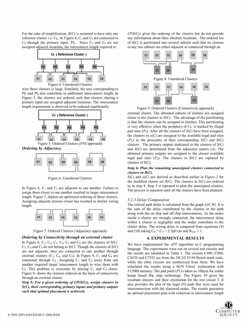
Ordering by Connectivity through an external clusterIn Figure 8, C1, C2, C3, C4, C5 and C6 are the clusters of S(C).C7, C8 and C9 do not belong to S(C). Though the clusters of S(C)are not adjacent, they are connected to one another through external clusters (C7, C8, and C9). In Figure 8. C1 and C4 are connected through C8. Assigning C1 and C4 away from one another required larger interconnect length to wire them with C8. This problem is overcome by placing C1 and C4 closer. Figure 9, shows the clusters ordered on the basis of connectivity through an external cluster.Step 5: For a given ordering of LP(S(C)), assign clusters in S(C), their corresponding primary inputs and primary outputs such that optimal placement is achieved.
LP(S(C)) gives the ordering of the clusters but do not provide any information about their absolute locations. The ordered list of S(C) is partitioned into several subsets such that no clusters in any two subsets are either adjacent or connected through an
Figure 8. Unordered Clusters
Figure 9. Ordered Clusters (Connectivity approach)external cluster. The obtained subsets of clusters are assigned closer to the clusters in R(C). The advantage of the partitioning is that the clusters can be assigned in batches. This partitioning is very effective when the periphery of CR is marked by illegal pad sites (Pil). After all the clusters of S(C) have been assigned, the clusters in α(C) are assigned to the available legal pad sites (Ple) in the proximity of their corresponding S(C) and R(C) clusters. The primary outputs dedicated to the clusters of S(C)and R(C) are determined from the adjacency matrix (A). The obtained primary outputs are assigned to the closest available legal pad sites (Ple). The clusters in R(C) are replaced by clusters of S(C).Step 6: Plan the remaining unassigned clusters connected to clusters in R(C).S(C) and α(C) are derived as described earlier in Figure 2 for the modified cluster set R(C). The clusters in S(C) are ordered as in step 4. Step 5 is repeated to plan the unassigned clusters. The process is repeated until all the clusters have been planned.
3.2.3 Delay ComputationThe critical path delay is calculated from the graph G(C,W). It is the sum of the delay contributed by the clusters in the path along with the on chip and off chip interconnects. As the nodes inside a cluster are strongly connected, the interconnect delaywithin a cluster is negligible and the nodes contribute to the cluster delay. The wiring delay is computed from equations (9) and (10) taking CH = CV = 2.5pF/cm and Rwire = 1.
4. EXPERIMENTAL RESULTSWe have implemented the APT algorithm in C programming language. The experiments were run on several test circuits and the results are tabulated in Table 1. The circuits C499, C880,C2670 and C7552 are from the ISCAS 85/89 Bench mark suite, while the other circuits are synthesized from them. We have simulated the results using a SUN Ultra2 workstation with 512MB memory. The pad pitch (P) is taken as 100µm for solder bump based flip chip technology. The Figure 10 gives the resultant clusters and their orientation for the test circuit 3. It also provides the plot of the legal I/O pads that were used for interconnection with the clustered nodes. The results guarantee an optimal placement plan with reduction in interconnect length
0-7695-2093-6/04 $20.00 2004 IEEE

(including both on-chip and off-chip parts) and delay by 10-15% over the existing iterative approach. The resultant delays are computed using equations (9) and (10) for the APT algorithm. Φ gives the execution time of APT algorithm. We also achieve a better speed up of over 10-15X over the iterative placement approach. The iterative approach that is used for comparisondeals with an initial assignment of the clusters inside the flip chip area. It plans them iteratively to get an optimal reduction in interconnect length and delay. The solution depends on the initial location. The execution time Ω is the time taken by the iterative algorithm to converge.
Figure 10. Resultant clusters and legal pad placementi: illegal pads, o: available legal pads, x: assigned pads
5. CONCLUSIONThe APT (Area I/O Planning Tool) algorithm provides a “total integrated solution” for placing the clustered nodes along withthe I/O pads in an area array based system. It provides a better non iterative planning approach for the SoC and SiP design methodologies. Experimental results on large test circuit's shows hat as a result of using the APT, the total interconnect length (including both on chip and off chip parts) and circuit
delay are significantly reduced by 10-15%. It also achieves a speed up of over 10-15X over the iterative method. In the future we plan to refine our algorithm for incorporating the area I/O buffer planning. 6. REFERENCES[1]An Intrinsic Area-Array Pad Router For ICs Chandra Tan,Donald Bouldin, Peyman Dehkordi. 17th Conference on Advanced Research in VLSI (ARVLSI '97)[2]Massoud Pedram, Kamal Chaudhary, Ernest S. Kuh: I/O PadAssignment Based on the Circuit Structure. ICCD 1991: 314-318. 1990[3]R. Farbarik, X. Liu, M. Rossman, P. Parakh, T. Basso,R. Brown,. "CAD Tools for Area-Distributed I/O Pad Packaging,” IEEE MCMC-97[4]F.E. Kiamilev, A.V. Krishnamoorthy, R.G. Rozier, G.F. Aplin, C.D. Hull, R. Farbarik and R.E. Oettel. Design of IC's for flip chip integration with optoelectronic device arrays, in proc Multichip module conf., pages 163-167, Santa Cruz, CA- 1997[5]Jason Cong, M'Lissa Smith: A Parallel Bottom-Up Clustering Algorithm with Applications to Circuit Partitioning in VLSI Design. DAC 1993: 755-760.[6]M. Hanan and JM Kurtzberg, A review of the placement and quadratic assignment problems. SIAM Review 14, 3-342 (1972).[7]Braun, T.; Becker, K.-F.; Koch, M.; Bader, V.; Aschenbrenner, R.; Reichl, H.; Flip Chip molding - Recent progress in flip chip encapsulation, Advanced Packaging Materials, 2002. Proceedings. 2002 8th International Symposium on , 3-6 March 2002, Page(s): 151 -159[8] A. E. Caldwell, A. B. Kahng, S. Mantik and I. L. Markov, "Implications of Area-Array I/O for Row-Based Placement Methodology", Proc. IEEE Symp. on IC/Package Design Integration, Santa Cruz, February 1998,.[9]Semiconductor industry association; National Technology Road map for Semiconductors: Technology needs (2001 edition), December 2001.
IL(mm) Delay (ns)Ckt # Nodes #I/P
#O/P APT IM APT IM
Φ(s)
Ω(s)
Test1 132 16 23 1 1.2 1.305 1.441 0.2 3.1Test2 150 30 35 2.2 2.5 1.095 1.232 0.6 8.9
Test3 156 18 24 1.9 2.2 1.560 1.731 0.7 9.6
Test4 230 45 53 4.6 5.2 1.832 2.043 1.1 15.4C880 383 60 26 2.1 2.5 1.045 1.211 1.7 22.8
C499 546 41 32 3.8 4.3 6.912 7.767 3.2 40.6Test5 880 66 64 5.3 6.1 9.982 11.19 6.1 87.3
C2670 1193 233 140 26.3 30.2 62.42 70.17 11.2 138.2
C7552 3512 207 108 7.6 8.9 28.52 32.39 14.3 208.4
Test6 5866 190 174 13.7 15.9 39.34 45.67 23.5 333.7
Test7 8984 263 240 18.3 21.7 47.38 58.45 31.3 460.3
Test8 11732 323 302 24.7 28.6 54.86 63.72 42.1 623.1
Table1. Experimental results of APT algorithm, IL: Interconnect length (including both on-chip and off-chip parts), Φ: speed of execution for the APT algorithm, Ω: speed of execution for iterative placement algorithm
0-7695-2093-6/04 $20.00 2004 IEEE
Related Documents