A 45nm Logic Technology with High-k + Metal Gate Transistors, Strained Silicon, 9 Cu Interconnect Layers, 193nm Dry Patterning, and 100% Pb-free Packaging K. Mistry , C. Allen, C. Auth, B. Beattie, D. Bergstrom, M. Bost, M. Brazier, M. Buehler, A. Cappellani, R. Chau * , C.-H. Choi, G. Ding, K. Fischer, T. Ghani, R. Grover, W. Han, D. Hanken, M. Hattendorf, J. He # , J. Hicks # , R. Heussner, D. Ingerly, P. Jain, R. James, L. Jong, S. Joshi, C. Kenyon, K. Kuhn, K. Lee, H. Liu, J. Maiz # , B. McIntyre, P. Moon, J. Neirynck, S. Pae # , C. Parker, D. Parsons, C. Prasad # , L. Pipes, M. Prince, P. Ranade, T. Reynolds, J. Sandford, L. Shifren % , J. Sebastian, J. Seiple, D. Simon, S. Sivakumar, P. Smith, C. Thomas, T. Troeger, P. Vandervoorn, S. Williams, K. Zawadzki Portland Technology Development, * CR, # QRE, % PTM Intel Corporation

Welcome message from author
This document is posted to help you gain knowledge. Please leave a comment to let me know what you think about it! Share it to your friends and learn new things together.
Transcript

A 45nm Logic Technology with High-k + Metal Gate Transistors, Strained Silicon, 9 Cu
Interconnect Layers, 193nm Dry Patterning, and 100% Pb-free Packaging
K. Mistry, C. Allen, C. Auth, B. Beattie, D. Bergstrom, M. Bost, M. Brazier, M. Buehler, A. Cappellani, R. Chau*, C.-H. Choi, G. Ding, K. Fischer, T. Ghani, R. Grover, W. Han, D. Hanken, M. Hattendorf, J. He#, J. Hicks#, R. Heussner, D. Ingerly, P. Jain, R. James, L. Jong, S. Joshi, C. Kenyon, K. Kuhn, K. Lee,
H. Liu, J. Maiz#, B. McIntyre, P. Moon, J. Neirynck, S. Pae#, C. Parker, D. Parsons, C. Prasad#, L. Pipes, M. Prince, P. Ranade, T. Reynolds,
J. Sandford, L. Shifren%, J. Sebastian, J. Seiple, D. Simon, S. Sivakumar, P. Smith, C. Thomas, T. Troeger, P. Vandervoorn, S. Williams, K. Zawadzki
Portland Technology Development, *CR, #QRE, %PTMIntel Corporation

2
Outline
• Introduction• Process Features• Transistors• Interconnects• Manufacturing• Conclusions

3
Introduction• SiON scaling running out of atoms• Poly depletion limits inversion TOX scaling
1
10
350nm 250nm 180nm 130nm 90nm 65nm
Elec
trica
l (In
v) T
ox (n
m)
0.01
0.1
1
10
100
1000
Gat
e Le
akag
e (R
el.)
Silicon
Poly
SiON

4
High-k + Metal Gate Benefits• High-k gate dielectric
– Reduced gate leakage– TOX scaling
• Metal gates– Eliminate polysilicon depletion– Resolves VT pinning and poor mobility
for high-k dielectrics

5
High-k + Metal Gate Challenges• High-k gate dielectric
– Poor mobility, VT pinning due to soft optical phonons
– Poor reliability
• Metal gates– Dual bandedge workfunctions– Thermal stability– Integration scheme

6
Outline
• Introduction• Process Features• Transistors • Interconnects• Manufacturing• Conclusions

7
Process Features
• 45 nm Groundrules• 193 nm Dry Lithography• High-K + Metal Gate Transistors• 3RD Generation Strained Silicon• Trench Contacts with Local Routing• 9 Cu Interconnect Layers• 100% Lead-free Packaging

8
Process Features
• 45 nm Groundrules• 193 nm Dry Lithography• High-K + Metal Gate Transistors• 3RD Generation Strained Silicon• Trench Contacts with Local Routing• 9 Cu Interconnect Layers• 100% Lead-free Packaging

9
45nm Design Rules
~0.7x linear scaling from 65nm
Layer Pitch (nm) Thick (nm) Aspect RatioIsolation 200 200
60144144144216252324
Metal 7 560 504 1.8Metal 8 810 720 1.8
7μm
--Contacted Gate 160 --Metal 1 160 1.8Metal 2 160 1.8Metal 3 160 1.8Metal 4 240 1.8Metal 5 280 1.8Metal 6 360 1.8
Metal 9 30.5μm 0.4

Contacted Gate Pitch• Transistor gate pitch of 160 nm continues
0.7x per generation scaling
Tightest contacted gate pitch reported for 45 nm generation
100
1000
250nm 180nm 130nm 90nm 65nm 45nm
Technology Node
Con
tact
ed G
ate
Pitc
h (n
m)
0.7x every 2 yearsPitch

11
SRAM Cells• 0.346 μm2 and 0.382 μm2 SRAM cells
– Optimize density and power/performance
Transistor density doubles every two years
0.1
1
10
250nm 180nm 130nm 90nm 65nm 45nm
Technology Node
SRA
M C
ell S
ize
( μm
2 )
0.5x every 2 years

12
SRAM Array Density• SRAM array density achieves 1.9 Mb/mm2
– Includes row/column drivers and other circuitry
Array density scales at ~2X per generation
1.9 Mb/mm2
0.1
1.0
10.0
90nm 65nm 45nmSRA
M A
rray
Den
sity
(Mb/
mm
2 )

13
Outline
• Introduction• Process Features• Transistors• Interconnects• Manufacturing• Conclusions

14
Transistor Process Flow• Key considerations
– Integrate hafnium-based high-k dielectric, dual metal gate electrodes, strained silicon
– Thermal stability of metal gate electrodes
• High-k First, Metal Gate Last– Metal gate deposition after high temperature
anneals– Integrated with strained silicon process– Transistor mask count same as 65nm

15a
Transistor Process Flow
p-well N-well
STI
Standard process except for ALD high-k
n-ext n-ext p-ext p-ext
High-k High-k
Dummy Polysilicon

15b
Transistor Process Flow
p-well N-well
STI
e-SiGe & S/D, Thermal anneal, ILD0 deposition
N+ N+ SiGeSiGe
ILD0
STI

15c
Transistor Process Flow
p-well N-well
STI
Poly Opening Polish
N+ N+ SiGeSiGeSTI

15d
Transistor Process Flow
p-well N-well
STI
Dummy Poly removal
N+ N+ SiGeSiGeSTI

15e
Transistor Process Flow
p-well N-well
STI
PMOS WF Metal deposition
N+ N+ SiGeSiGeSTI

15f
Transistor Process Flow
p-well N-well
STI
PMOS WF Metal patterning
N+ N+ SiGeSiGeSTI

15g
Transistor Process Flow
p-well N-well
STI
NMOS WF Metal deposition
N+ N+ SiGeSiGeSTI

15h
Transistor Process Flow
p-well N-well
STI
Metal Gate trenches filled with low resistance Al
N+ N+ SiGeSiGe
Al fill
STI

15i
Transistor Process Flow
p-well N-well
STI
Metal Gate Polish
N+ N+ SiGeSiGeSTI

15j
Transistor Process Flow
p-well N-well
STIN+ N+ SiGeSiGeSTI
High-k High-k
NMOS WF PMOS WF
Low Resistance Al Fill
High-k + Metal gate transistor formation complete

16
Transistor Features
• 35 nm min. gate length• 160 nm contacted gate
pitch
• 1.0 nm EOT Hi-K• Dual workfunction
metal gate electrodes
• 3RD generation of strained silicon

17
Gate Leakage • Gate leakage is reduced >25X for NMOS
and 1000X for PMOS
0.00001
0.0001
0.001
0.01
0.1
1
10
100
-1.2 -1 -0.8 -0.6 -0.4 -0.2 0 0.2 0.4 0.6 0.8 1 1.2
VGS (V)
Nor
mal
ized
Gat
e Le
akag
e SiON/Poly 65nm
HiK+MG 45nm
NMOS PMOS
HiK+MG 45nm
SiON/Poly 65nm
65nm: Bai, 2004 IEDM

18
Optimal Workfunction Metals• Excellent VT rolloff and DIBL
NMOS PMOS
0.00
0.05
0.10
0.15
0.20
0.25
0.30
0.35
0.40
0.45
0.50
30 35 40 45 50 55 60LGATE (nm)
Thre
shol
d Vo
ltage
(V)
|VDS|= 1.0V
|VDS|= 0.05V
-0.50
-0.45
-0.40
-0.35
-0.30
-0.25
-0.20
-0.15
-0.10
-0.05
0.00
30 35 40 45 50 55 60LGATE (nm)
Thre
shol
d Vo
ltage
(V)
|VDS|= 1.0V
|VDS|= 0.05V

19
3RD Generation Strained Silicon
• Increased Gefraction– 90 nm: 17% Ge– 65 nm: 23% Ge– 45 nm: 30% Ge
• SiGe closer to channel

20
NMOS IDSAT vs. IOFF
1.36 mA/μm at IOFF = 100 nA/μm12% better than 65 nm
1
10
100
1000
0.8 0.9 1.0 1.1 1.2 1.3 1.4 1.5 1.6IDSAT (mA/μm)
IOFF
(nA
/ μm
)
65 nm
VDD = 1.0V
90 nm
160 nm
90nm: Mistry 2004 VLSI65nm: Tyagi, 2005 IEDM
21
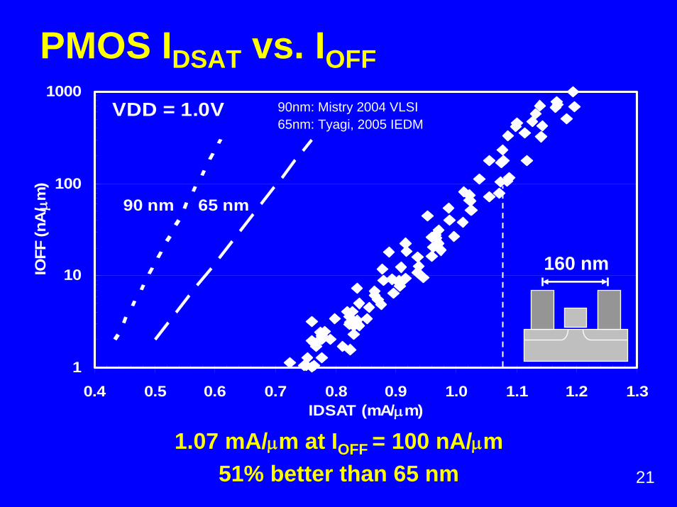
PMOS IDSAT vs. IOFF
1.07 mA/μm at IOFF = 100 nA/μm51% better than 65 nm
1
10
100
1000
0.4 0.5 0.6 0.7 0.8 0.9 1.0 1.1 1.2 1.3IDSAT (mA/μm)
IOFF
(nA
/ μm
)
65 nm
VDD = 1.0V
90 nm
160 nm
90nm: Mistry 2004 VLSI65nm: Tyagi, 2005 IEDM

22
Transistor Performance vs. Gate Pitch
Simultaneous performance and density improvement
90nm: Mistry, 2004 VLSI65nm: Tyagi, 2005 IEDM
1001000 Contacted Gate Pitch (nm)
IDSA
T (m
A/ μ
m)
0.0
0.2
0.4
0.6
0.8
1.0
1.2
1.4
1.6
PMOS
NMOS
160nm (45nm)
220nm (65nm)
320nm (90nm)
1.0V, 100 nA/μm
Gate Pitch (Generation)

23
Ring Oscillator Performance
3
4
5
6
7
8
9
10 100 1000 10000IOFFN + IOFFP (nA/um)
DEL
AY
PER
STA
GE
(pS)
65nm @ 1.2V
45nm @1.1V
Fanout = 2
FO=2 delay of 5.1 ps at IOFFN = IOFFP = 100 nA/μm23% better than 65 nm at the same leakage

24
Transistor Reliability Challenges
• Defect types in SiO2 have been studied for decades
• New defect types for high-k need to be suppressed
• TINV scaled ~0.7X relative to 65 nm– Need to support 30% higher E-field

25
Transistor Reliability - TDDB
45nm High-k + Metal Gate supports 30% higher E-field
1.E+02
1.E+03
1.E+04
1.E+05
1.E+06
1.E+07
1.E+08
1.E+09
4 6 8 10 12 14 16Field (MV/cm)
TDD
B (s
ec)
SiON/Poly 65nm
45nmHK+MG
65nm: Bai, 2004 IEDM

26
Transistor Reliability: Bias Temperature
0
10
20
30
40
50
5 7 9 11 13SiO2 equivalent EField (MV/cm)
Vt i
ncre
ase
(mV
)
SiON/Poly 65nm
45nm HK+MG
PMOS NBTI
0
10
20
30
40
50
5 7 9 11 13SiO2 equivalent EField (MV/cm)
Vt i
ncre
ase
(mV
)
45nm HK+MG
SiON/Poly65nm
NMOS PBTI
PMOS NBTI 45 nm Hi-k + MG supports 50% higher E-field
NMOS PBTI 45 nm Hi-k + MG supports 15% higher E-field
65nm: Bai, 2004 IEDM

27
Outline
• Introduction• Process Features• Transistors• Interconnects• Manufacturing• Conclusions

28
Interconnects • Metal 1-3 pitches
match transistor pitch
• Graduated upper level pitches optimize density & performance
• Lower layer SiCNetch stop layer thinned 50% relative to 65 nm
• Extensive use of low-k ILD
MT1MT2MT3
MT7
MT4
MT5
MT8
MT6
CDOCDOCDO
CDO
CDO
CDO
CDO
SiO2

29
Metal 9: ReDistribution Layer (RDL) • Metal 9 RDL: 7um thick with polymer ILD
– Improved on-die power distribution
Polymer ILD
Cu Bump
Metal 9
MT8MT7
7 μm

30
100% Lead Free Packaging
Cu Bump
Sn/Ag/Cu Solder
Cu Pad
45 nm
65 nm
Cu Bump
Pb/Sn Solder
Cu Pad
90 nm
Pb Bump
Cu Pad
Pb/Sn Solder
• Environmental benefit, lower SER
31
Outline
• Introduction• Process Features• Transistors• Interconnects• Manufacturing• Conclusions

32
153Mb SRAM Test Vehicle• Process learning vehicle demonstrates
– High yield– High performance– Stable low voltage operation
1.3V |***************************** .
1.2V |************************** .
1.1V |************************* .
1.0V |********************** .
0.9V |**************** . .
0.8V |****** . . .+---------+---------+---------+1.8GHz 2.3GHz 3.2GHz 5.3GHz
3.8GHz
2GHz
4.7GHz
0.346 μm2 SRAM Cell>1 billion transistors
Fully functional Jan’06

33
Multiple Microprocessors
Single Core
Dual Core
Quad Core

Defect Reduction Trend• Mature yield demonstrated 2 years after 65 nm
Defect Density (log scale)
2000 2001 2002 2003 2004 2005 2006 2007 2008
130 nm 90 nm 65 nm 45 nm

Defect Reduction Trend• Mature yield demonstrated 2 years after 65 nm• Matched yield in 2ND Fab – Copy Exactly!
Defect Density (log scale)
2000 2001 2002 2003 2004 2005 2006 2007 2008
F32
130 nm 90 nm 65 nm 45 nm

35
Conclusions• A 45 nm technology is described with
– Design rules supporting ~2X improvement in transistor density– 193nm dry lithography at critical layers for low cost– Trench contacts supporting local routing– 8 standard Cu interconnect layers with extensive use of low-k– Thick Metal 9 Cu RDL with polymer ILD
• High-k + Metal gate transistors implemented for the first time in a high volume manufacturing process– Integrated with 3RD generation strained silicon– Achieve record drive currents at low IOFF and tight gate pitch
• The technology is already in high volume manufacturing– High yields demonstrated on SRAM and 3 microprocessors– High yields demonstrated in two 300mm fabs

36
Acknowledgements
• The authors gratefully acknowledge the many people in the following organizations at Intel who contributed to this work:– Portland Technology Development – Quality and Reliability Engineering– Process & Technology Modeling– Assembly & Test Technology Development

37
For further information on Intel's silicon technology, please visit our Technology & Research page at
www.intel.com/technology
Related Documents