1440 iEEE JOURNAL OF SOLID-STATE CIRCUITS, VOL. 29, NO. 12, DECEMBER 1994 A 2.2 W, 80 MHz Superscalar RISC Microprocessor Gian Gerosa, Member, IEEE, Sonya Gary, Carl Dietz, Dac Pham, Kathy Hoover, Jose Alvarez, Member, IEEE, Hector Sanchez, Pete Ippolito, Tai Ngo, Suzanne Litch, Member, IEEE, Jim Eno, Jim Golab, Member, IEEE, Neil Vanderschaaf, Member, IEEE, and Jim Kahle Abstract-A 28 mW/MHz at 80 MHz structured-custom RISC microprocessor design is described [l]. This 32-b implementation of the PowerPCTR’architecture is fabricated in a 3.3 V, 0.5 pm, 4-level metal CMOS technology, resulting in 1.6 million transistors in a 7.4 mm by 11.5 mm chip size. Dual 8-kilobyte instruction and data caches coupled to a high performance 32/64- b system bus and separate execution units (float, integer, load- store, and system units) result in peak instruction rates of three instructions per clock cycle. Low-power design techniques are used throughout the entire design, including dynamically powered down execution units. ‘Qpical power dissipation is kept under 2.2 W at 80 MHz. Three distinct levels of software-programmable, static, low-power operation-for system power management are offered, resulting in standby power dissipation from 2 mW to 350 mW. CPU to Bus clock ratios of l x , 2x, 3x, and 4 x are implemented to allow control of system power while maintaining processor performance. As a result, workstation- level performance is packed into a low-power, low-cost design ideal for notebooks and desktop computers. I. INTRODUCTION HE PowerPC 603TnfMicroprocessor’ is the second mem- T ber of the PowerPCThl microprocessor family. The de- sign is a superscalar implementation, featuring low-power operation and several battery-saving static power management modes. Maximum operating frequency is 80 MHz at a VDD supply of 3.0 V, a junction temperature of 105OC, and typical silicon processing. At 3.3 V, typical power dissipation for normal operation is 2.2 W, while standby power dissipation ranges from 350 mW down to 2 mW using doze, nap and sleep static power management modes. The 1.6 million transistor design is implemented in a low-cost 0.5 pm, four level metal, 3.3 V CMOS technology. The 84.8 mm2 design features dual 8-kilobyte instruction and data caches, a floating-point unit, an integer unit, a loadstore unit, a system unit and a high-performance 32/64-b system bus. Up to three instruc- tions per cycle can be dispatched in this superscalar design, achieving an estimated performance of 75 SPECint92TMand 85 sPECf~92~~ at 80 MHz with a 1 megabyte external Manuscript received May 12, 1994; revised June 7, 1994 and Aug. 24, 1994. G. Gerosa, S. Gary, J. Alvarez, H. Sanchez, S. Litch, J. Eno, and J. Golab are with Motorola, Inc., Austin, TX 78759 USA. C. Dietz. D. Pham, K. Hoover, P. Ippolito, T. Ngo, N. Vanderschaaf, and J. Kahle are with International Business Machines Corporation, Somerset Design Center, Austin, TX 78759 USA. IEEE Log Number 9406253. ’ The terms “PowerPC 603 Microprocessor” and “603” are used to denote the second microprocessor from the PowerPC Architecture family. PowerPC, PowerPC Architecture, PowerPC 603, and RISC Systed6000 are trademarks of International Business Machines Corporation. SPEC, SPECint92, and SPECfp92 are trademarks of Standard Performance Evaluation Corporation. secondary cache. The design’s user-configurable, multiplying PLL provides a processor clock at 1 x, 2 x , 3 x or 4 x the bus clock frequency. Testability features include level-sensitive- scan-design (LSSD), array-built-in-self-test (ABIST) logic for cache and tag arrays, and a JTAG interface. A structured custom approach is used to build this VLSI design. Synthesized logic is placed and routed with standard cells. Datapaths are placed and routed using custom macros designed to conform to a specific chip image. These datapath elements cover a broad range of designs from simple nand gates up to 8-kilobyte cache arrays. 11. MICROARCHITECTURE This RISC microprocessor design is based on a new mi- croarchitecture that is optimized for portable applications. The microprocessor design features a high performance-to- transistor ratio and independent execution units that maximize the effectiveness of power management. It is a dual-issue superscalar implementLtion with branch folding for a max- imum throughput of three instructions per cycle [2], [4]. Performance/area trade-offs are crucial in the design. An example of this is the use of software tablewalks to reduce transistor count at the expense of system performance. A block diagram of the design is shown in Fig. 1. Up to two instructions per clock cycle are fetched from the instruction cache and sent to both the instruction buffer and the branch unit. The branch unit decodes and executes branch instructions and deletes them from the instruction buffer (branch folding). The instruction buffer supplies instructions to a primary in- struction decoder which can dispatch up to two instructions per clock cycle. in program order, to any of four execution units: fixed-point unit (FXU), system unit (SYSU), loadktore unit (LSU), and floating-point unit (FPU). Operands from the general purpose register (GPR) file and/or floating-point register (FPR) file are read during the dispatch cycle. Each execution unit has a reservation station so that instructions can be dispatched regardless of whether all operands are available. When an operand becomes available after instruction dispatch, it is forwarded to the unit and the instruction is executed. Register renaming is used to reduce register dependency delays and to provide support for both precise exceptions and speculative execution. Once dispatched, instructions are allowed to execute out of order (in order within each function unit). A completion buffer mechanism tracks execution and controls retirement of up to two instructions per clock cycle in program order. 0018-9200/94$04.00 0 1994 IEEE

Welcome message from author
This document is posted to help you gain knowledge. Please leave a comment to let me know what you think about it! Share it to your friends and learn new things together.
Transcript
1440 iEEE JOURNAL OF SOLID-STATE CIRCUITS, VOL. 29, NO. 12, DECEMBER 1994
A 2.2 W, 80 MHz Superscalar RISC Microprocessor Gian Gerosa, Member, IEEE, Sonya Gary, Carl Dietz, Dac Pham, Kathy Hoover,
Jose Alvarez, Member, IEEE, Hector Sanchez, Pete Ippolito, Tai Ngo, Suzanne Litch, Member, IEEE, Jim Eno, Jim Golab, Member, IEEE, Neil Vanderschaaf, Member, IEEE, and Jim Kahle
Abstract-A 28 mW/MHz at 80 MHz structured-custom RISC microprocessor design is described [l]. This 32-b implementation of the PowerPCTR’ architecture is fabricated in a 3.3 V, 0.5 pm, 4-level metal CMOS technology, resulting in 1.6 million transistors in a 7.4 mm by 11.5 mm chip size. Dual 8-kilobyte instruction and data caches coupled to a high performance 32/64- b system bus and separate execution units (float, integer, load- store, and system units) result in peak instruction rates of three instructions per clock cycle. Low-power design techniques are used throughout the entire design, including dynamically powered down execution units. ‘Qpical power dissipation is kept under 2.2 W at 80 MHz. Three distinct levels of software-programmable, static, low-power operation-for system power management are offered, resulting in standby power dissipation from 2 mW to 350 mW. CPU to Bus clock ratios of l x , 2 x , 3 x , and 4 x are implemented to allow control of system power while maintaining processor performance. As a result, workstation- level performance is packed into a low-power, low-cost design ideal for notebooks and desktop computers.
I. INTRODUCTION
HE PowerPC 603TnfMicroprocessor’ is the second mem- T ber of the PowerPCThl microprocessor family. The de- sign is a superscalar implementation, featuring low-power operation and several battery-saving static power management modes. Maximum operating frequency is 80 MHz at a VDD supply of 3.0 V, a junction temperature of 105OC, and typical silicon processing. At 3.3 V, typical power dissipation for normal operation is 2.2 W, while standby power dissipation ranges from 350 mW down to 2 mW using doze, nap and sleep static power management modes. The 1.6 million transistor design is implemented in a low-cost 0.5 pm, four level metal, 3.3 V CMOS technology. The 84.8 mm2 design features dual 8-kilobyte instruction and data caches, a floating-point unit, an integer unit, a loadstore unit, a system unit and a high-performance 32/64-b system bus. Up to three instruc- tions per cycle can be dispatched in this superscalar design, achieving an estimated performance of 75 SPECint92TM and 85 s P E C f ~ 9 2 ~ ~ at 80 MHz with a 1 megabyte external
Manuscript received May 12, 1994; revised June 7, 1994 and Aug. 24, 1994.
G. Gerosa, S . Gary, J. Alvarez, H. Sanchez, S. Litch, J . Eno, and J. Golab are with Motorola, Inc., Austin, TX 78759 USA.
C. Dietz. D. Pham, K. Hoover, P. Ippolito, T. Ngo, N. Vanderschaaf, and J. Kahle are with International Business Machines Corporation, Somerset Design Center, Austin, TX 78759 USA.
IEEE Log Number 9406253. ’ The terms “PowerPC 603 Microprocessor” and “603” are used to denote the second microprocessor from the PowerPC Architecture family. PowerPC, PowerPC Architecture, PowerPC 603, and RISC Systed6000 are trademarks of International Business Machines Corporation.
SPEC, SPECint92, and SPECfp92 are trademarks of Standard Performance Evaluation Corporation.
secondary cache. The design’s user-configurable, multiplying PLL provides a processor clock at 1 x, 2 x , 3 x or 4 x the bus clock frequency. Testability features include level-sensitive- scan-design (LSSD), array-built-in-self-test (ABIST) logic for cache and tag arrays, and a JTAG interface.
A structured custom approach is used to build this VLSI design. Synthesized logic is placed and routed with standard cells. Datapaths are placed and routed using custom macros designed to conform to a specific chip image. These datapath elements cover a broad range of designs from simple nand gates up to 8-kilobyte cache arrays.
11. MICROARCHITECTURE
This RISC microprocessor design is based on a new mi- croarchitecture that is optimized for portable applications. The microprocessor design features a high performance-to- transistor ratio and independent execution units that maximize the effectiveness of power management. It is a dual-issue superscalar implementLtion with branch folding for a max- imum throughput of three instructions per cycle [2], [4]. Performance/area trade-offs are crucial in the design. An example of this is the use of software tablewalks to reduce transistor count at the expense of system performance.
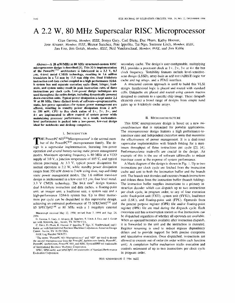
A block diagram of the design is shown in Fig. 1. Up to two instructions per clock cycle are fetched from the instruction cache and sent to both the instruction buffer and the branch unit. The branch unit decodes and executes branch instructions and deletes them from the instruction buffer (branch folding). The instruction buffer supplies instructions to a primary in- struction decoder which can dispatch up to two instructions per clock cycle. in program order, to any of four execution units: fixed-point unit (FXU), system unit (SYSU), loadktore unit (LSU), and floating-point unit (FPU). Operands from the general purpose register (GPR) file and/or floating-point register (FPR) file are read during the dispatch cycle. Each execution unit has a reservation station so that instructions can be dispatched regardless of whether all operands are available. When an operand becomes available after instruction dispatch, it is forwarded to the unit and the instruction is executed. Register renaming is used to reduce register dependency delays and to provide support for both precise exceptions and speculative execution. Once dispatched, instructions are allowed to execute out of order (in order within each function unit). A completion buffer mechanism tracks execution and controls retirement of up to two instructions per clock cycle in program order.
0018-9200/94$04.00 0 1994 IEEE
Idsatn I Idsatp: ux)I 130pVpn
METALS (AL) width I contacted pitch I resistance (mohndsquare)
transistors 1.6 million
GEROSA er al.: SUPERSCALAR RlSC MICROPROCESSOR 1441
TABLE I P R W E S S FEATURES AND CHIP CHARACTERISTICS
I 1
I technology: I 0.5 pm N-well CMOS with p- epi on p+ substrate
I gateoxide: I 13.5 nm I I Leffn/ ~ e f f p : I 0.45 10.50 p I I Vm I VIP: I 0.60 1-0.80 volts I
I metal2. metal3 I 0.9 I 1.8 155.0 I 2.4 14.8 I 18.0 last metal + I , I I
I I input/output buffers I 165 signals. 5 volt tolerant; 75 power pins I L
Fig. I . 603 block diagram
Packase wirebond CQFP and C4QFP
cache I split 8KB icache and 8KB dcache
register files 32X64(floaI) and 32X32Cinteger)
CPU to bus ratios I 1x. 2x. 3x, 4x To support architectural features such as speculative execu-
tion, this implementation uses several unique circuit solutions. Data is held on each rename bus with a special keeper circuit. The rename buses forward results to both the execution units and the register files. Another circuit solution for speculative execution is a logic array that resolves register dependencies and determines execution unit status in the dispatch stage. This allows single-cycle dispatch to multiple units with multiple rename buses.
BUS bandwidth
power
16MHz < SYSCLK < 66MHz
I 2.2W @ 80MHz and 2X mode
5 0
4 5
4 0
35
6, 30 o - f 25
5 2 0
1s
10
5
0
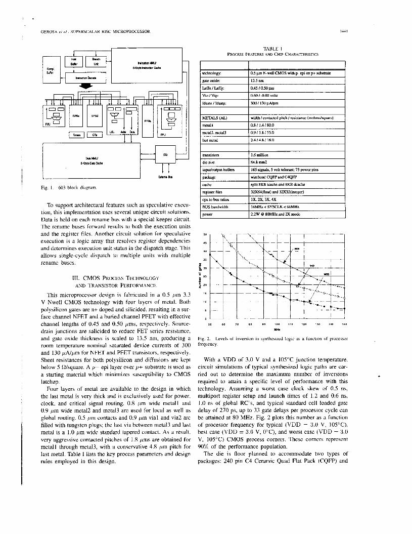
111. CMOS PROCESS TECHNOLOGY AND TRANSISTOR PERFORMANCE
This microprocessor design is fabricated in a 0.5 pm 3.3 V Nwell CMOS technology with four layers of metal. Both polysilicon gates are n+ doped and silicided, resulting in a sur- face channel NFET and a buried channel PFET with effective channel lengths of 0.45 and 0.50 pms, respectively. Source- drain junctions are salicided to reduce FET series resistance, and gate oxide thickness is scaled to 13.5 nm, producing a room temperature nominal saturated device currents of 300 and 130 p N p m for NFET and PFET transistors, respectively. Sheet resistances for both polysilicon and diffusions are kept below 5 Rlsquare. A p - epi layer over y+ substrate is used as a starting material which minimizes susceptibility to CMOS latchup.
Four layers of metal are available to the design in which the last metal is very thick and is exclusively used for power, clock, and critical signal routing. 0.8 pm wide metal1 and 0.9 pm wide metal2 and metal3 are used for local as well as global routing. 0.5 pm contacts and 0.9 pm vial and via2 are filled with tungsten plugs; the last via between metal3 and last metal is a 1.0 pm wide standard tapered contact. As a result, very aggressive contacted pitches of 1.8 pms are obtained for metal1 through metal3, with a conservative 4.8 pm pitch for last metal. Table I lists the key process parameters and design rules employed in this design.
50 BO 7 0 80 90 100 110 120 130 1 4 0 I 5 0
y m
Fig. 2 . frequency.
Levels of inversion in synthesized logic as a function of processor
With a VDD of 3.0 V and a 105°C junction temperature, circuit simulations of typical synthesized logic paths are car- ried out to determine the maximum number of inversions required to attain a specific level of performance with this technology. Assuming a worst case clock skew of 0.5 ns, multiport register setup and launch times of 1.2 and 0.6 ns, 1.0 ns of global RC's, and typical standard cell loaded gate delay of 270 ps, up to 33 gate delays per processor cycle can be attained at 80 MHz. Fig. 2 plots this number as a function of processor frequency for typical (VDD = 3.0 V, 105"C), best case (VDD = 3.6 V, OOC), and worst case (VDD = 3.0 V, 105OC) CMOS process comers. These corners represent 90% of the performance population.
The die is floor planned to accommodate two types of packages: 240 pin C4 Ceramic Quad Flat Pack (CQFP) and
I342 IEEE JOURNAL OF SOLID-STATE CIRCUITS, VOL. 29, NO. 12, DECEMBER 1993
240 pin wire bond CQFP. The off-chip drivers are placed on
and GND power rails. A single last metal design includes a 129.6 iim wire bond pad pitch and a 250 pm C4 pad pitch
the perimeter of the chip with split intemal and external VDD Data cache
- - .~ arrangement. The chip has 165 signal pads and 75 power and ground pads.
lnstrUcth Cache
This microprocessor implementation uses a common set of 0.5 pm layout rules to guarantee similar levels of performance
fabs. Differences are limited to isolation technology (shallow
L C d Store and manufacturability from both Motorola and IBM wafer
trench vs. aggressive LOCOS) and nwell formation (retrograde vs. standard). Fold-
POinl
IV. POWER MANAGEMENT
power dissipation under 2.2 W at 80 MHz and in the milliwatt range dnring standby. Low normal-mode power dissipation is achieved through a reduced supply voltage of 3.3 V, a fully static CMOS design, low-power standard cell and datapath library design, and dynamic power management. Dynamic
areas of the chip based on the level of activity required to run a particular application [3] . This reduces the amount of unnecessary power dissipated during normal operation. Low
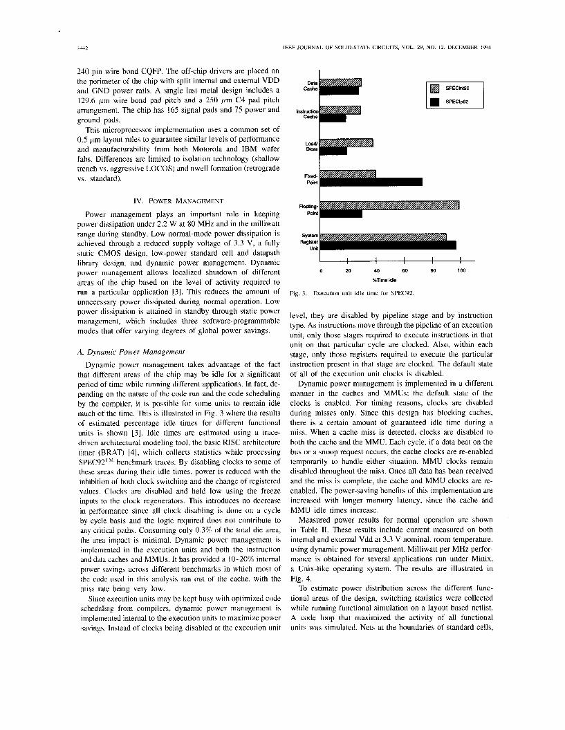
Floating- Point Power management plays an important role in keeping
system R q U w
ukrYxYY- power management allows localized shutdown of different 0 20 40 60 80 100
%"e Idle
~ i ~ , 3 , ~~~~~~i~~ ,,"it idle for SpEf-92,
power dissipation is attained in standby through static power management, which includes three software-programmable modes that offer varying degrees of global power savings.
level, they are disabled by pipeline stage and by instruction type. As instructions move through the pipeline of an execution unit, only those stages required to execute instructions in that
A. Dynamic Power Management
Dynamic power management takes advantage of the fact that different areas of the chip may be idle for a significant period of time while running different applications. In fact, de- pending on the nature of the code run and the code scheduling by the compiler, it is possible for some units to remain idle much of the time. This is illustrated in Fig. 3 where the results of estimated percentage idle times for different functional units is shown [3J. Idle times are estimated using a trace- driven architectural modeling tool, the basic RISC architecture timer (BRAT) 141, which collects statistics while processing SPEC92TM benchmark traces. By disabling clocks to some of these areas during their idle times, power is reduced with the inhibition of both clock switching and the change of registered values. Clocks are disabled and held low using the freeze inputs to the clock regenerators. This introduces no decrease in performance since all clock disabling is done on a cycle by cycle basis and the logic required does not contribute to any critical paths. Consuming only 0.3% of the total die area, the area impact is minimal. Dynamic power management is implemented in the execution units and both the instruction and data caches and MMUs. It has provided a l0-20% internal power savings across different benchmarks in which most of the code used in this analysis ran out of the cache, with the miss rate being very low.
Since execution units may be kept busy with optimized code scheduling from compilers, dynamic power management is implemented intemal to the execution units to maximize power savings. Instead of clocks being disabled at the execution unit
unit on that particular cycle are clocked. Also, within each stage, only those registers required to execute the particular instruction present in that stage are clocked. The default state of all of the execution unit clocks is disabled.
Dynamic power management is implemented in a different manner in the caches and MMUs; the default state of the clocks is enabled. For timing reasons, clocks are disabled during misses only. Since this design has blocking caches, there is a certain amount of guaranteed idle time during a miss. When a cache miss is detected, clocks are disabled to both the cache and the MMU. Each cycle, if a data beat on the bus or a snoop request occurs, the cache clocks are re-enabled temporarily to handle either situation. MMU clocks remain disabled throughout the miss. Once all data has been received and the miss is complete, the cache and MMU clocks are re- enabled. The power-saving benefits of this implementation are increased with longer memory latency, since the cache and MMU idle times increase.
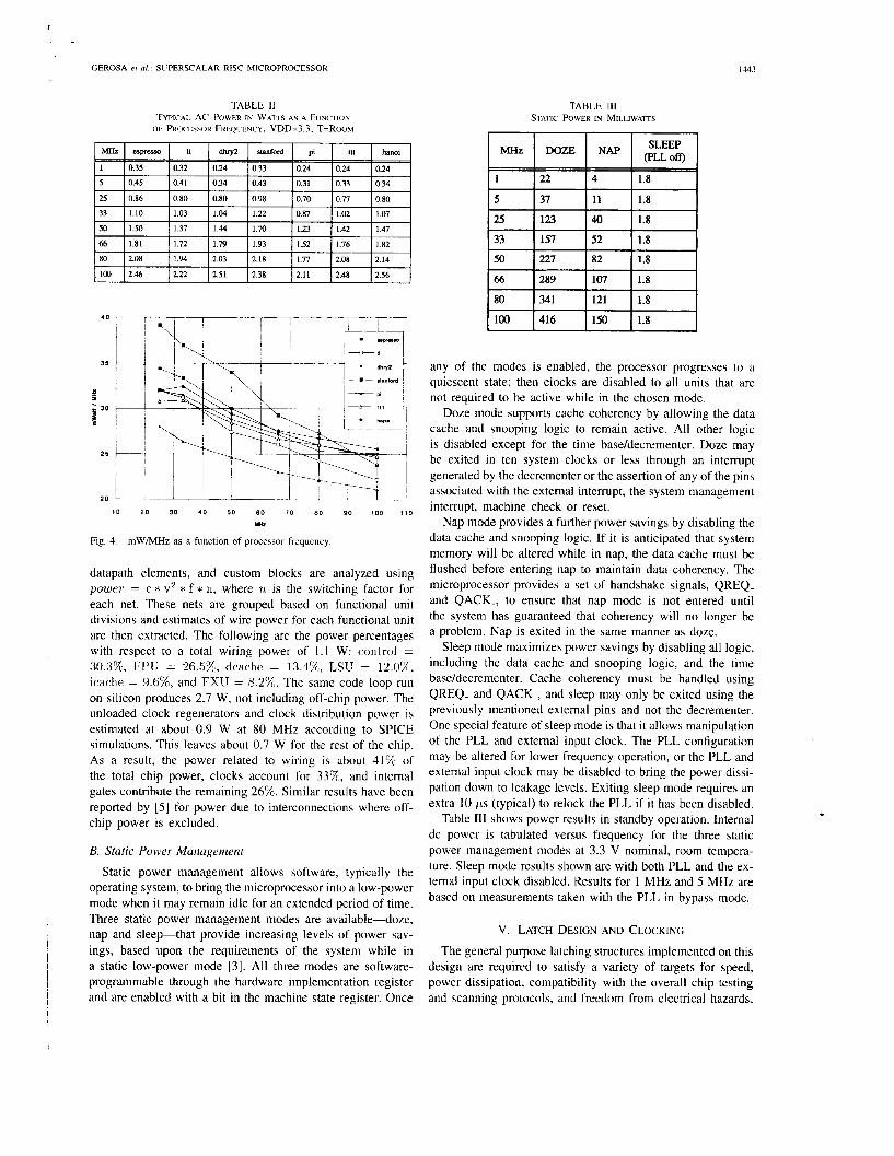
Measured power results for normal operation are shown in Table 11. These results include current measured on both intemal and extemal Vdd at 3.3 V nominal, room temperature, using dynamic power management. Milliwatt per MHz perfor- mance is obtained for several applications run under Minix, a Unix-like operating system. The results are illustrated in Fig. 4.
To estimate power distribution across the different func- tional areas of the design, switching statistics were collected while running functional simulation on a layout-based netlist. A code loop that maximized the activity of all functional units was simulated. Nets at the boundaries of standard cells,
GEROSA et al.: SUPERSCALAR RISC MICROPROCESSOR
MHZ I espresso I li I dhry~
1443
stanford pi tn hanoi
TABLE I1 TYPICAL AC POWER IN WATS AS A FUNCTION
OF PROCESSOR FREQUENCY, VDD=3.3, T=Rooh~
5
25
33
50
0.45 0.41 0.34 0.43 0.31 0.33 0.34
0.86 0.80 0.80 0.98 0.70 0.77 0.80
1.10 1.03 1.04 1.22 0.87 1.02 1.07
1.50 1.37 1.44 1.70 1.23 1.42 1.47
66
80
100
1.81 1.72 1.79 1.93 1.52 1.76 1.82
2.08 1.94 2.03 2.18 1.77 2.08 2.14
2.46 2.22 2.51 2.38 2.11 2.48 2.56
35
; 2 30
25
66
80
I 10 20 30 40 5 0 6 0 7 0 8 0 90 100 110
YLI
Fig 4 mW/MHz as a function of procesyor frequency
289 107 1.8
34 1 121 1.8
datapath elements, and custom blocks are analyzed using powrr = c * v2 * f * 11, where n is the switching factor for each net. These nets are grouped based on functional unit divisions and estimates of wire power for each functional unit are then extracted. The following are the power percentages with respect to a total wiring power of 1 .1 W: control = 30.30/,, FPU = 26.5%, dcachc = 13.3%, LSU = l2.0%, icache = Y.C;%, and FXU = 8.2%. The same code loop run on silicon produces 2.7 W, not including off-chip power. The unloaded clock regenerators and clock distribution power is estimated at about 0.9 W at 80 MHz according to SPICE simulations. This leaves about 0.7 W for the rest of the chip. As a result, the power related to wiring is about 41%) of the total chip power, clocks account for 33%, and internal gates contribute the remaining 26%. Similar results have been reported by [5] for power due to interconnections where off- chip power is excluded.
B. Static Power Management
Static power management allows software, typically the operating system, to bring the microprocessor into a low-power mode when it may remain idle for an extended period of time. Three static power management modes are available-doze, nap and sleep-that provide increasing levels of power sav- ings, based upon the requirements of the system while in a static low-power mode [3]. All three modes are software- programmable through the hardware implementation register and are enabled with a bit in the machine state register. Once
TABLE 111 STATIC POWER IN MILLIWATTS
123 1.8
157 52 1.8
I 1100 I 416 I150 11.8
any of the modes is enabled, the processor progresses to a quiescent state; then clocks are disabled to all units that are not required to be active while in the chosen mode.
Doze mode supports cache coherency by allowing the data cache and snooping logic to remain active. All other logic is disabled except for the time base/decrementer. Doze may be exited in ten system clocks or less through an interrupt generated by the decrementer or the assertion of any of the pins associated with the extemal interrupt, the system management interrupt, machine check or reset.
Nap mode provides a further power savings by disabling the data cache and snooping logic. If it is anticipated that system memory will be altered while in nap, the data cache must be flushed before entering nap to maintain data coherency. The microprocessor provides a set of handshake signals, QREQ- and QACK-, to ensure that nap mode is not entered until the system has guaranteed that coherency will no longer be a problem. Nap is exited in the same manner as doze.
Sleep mode maximizes power savings by disabling all logic, including the data cache and snooping logic, and the time base/decrementer. Cache coherency must be handled using QREQ- and QACK-, and sleep may only be exited using the previously mentioned external pins and not the decrementer. One special feature of sleep mode is that it allows manipulation of the PLL and external input clock. The PLL configuration may be altered for lower frequency operation, or the PLL and extemal input clock may be disabled to bring the power dissi- pation down to leakage levels. Exiting sleep mode requires an extra 10 ps (typical) to relock the PLL if it has been disabled.
Table 111 shows power results in standby operation. Internal dc power is tabulated versus frequency for the three static power management modes at 3.3 V nominal, room tempera- ture. Sleep mode results shown are with both PLL and the ex- ternal input clock disabled. Results for 1 MHz and 5 MHz are based on measurements taken with the PLL in bypass mode.
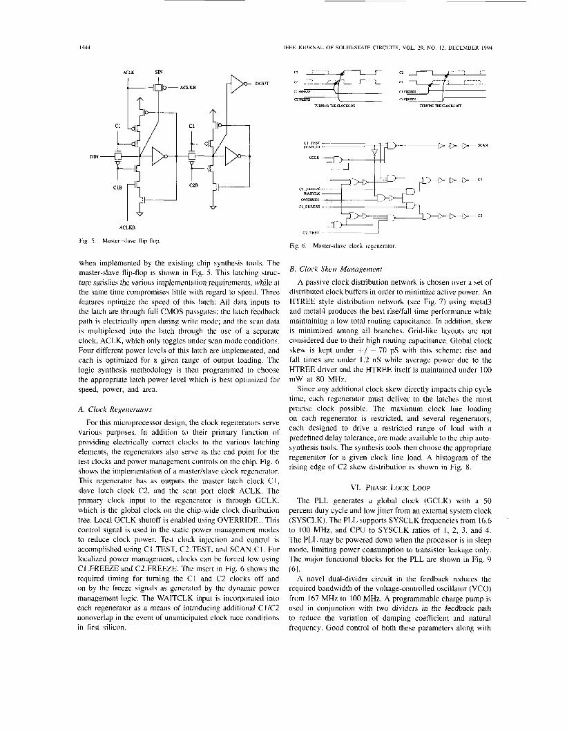
v. LATCH DESIGN AND CLOCKING
The general purpose latching structures implemented on this design are required to satisfy a variety of targets for speed, power dissipation, compatibility with the overall chip testing and scanning protocols, and freedom from electrical hazards,
1444 IEEE JOURNAL OF SOLID-STATE CIKCUITS. VOL. 29. NO. 12. DECEMBER 1994
Fig
DOUT
DIN
I * ACLKB
. 5. Master-slave flip-flop
when implemented by the existing chip synthesis tools. The master-slave flip-flop is shown in Fig. 5. This latching struc- ture satisfies the various implementation requirements, while at the same time compromises little with regard to speed. Three features optimize the speed of this latch: All data inputs to the latch are through full CMOS passgates; the latch feedback path is electrically open during write mode; and the scan data is multiplexed into the latch through the use of a separate clock, ACLK, which only toggles under scan mode conditions. Four different power levels of this latch are implemented, and each is optimized for a given range of output loading. The logic synthesis methodology is then programmed to choose the appropriate latch power level which is best optimized for speed, power, and area.
A. Clock Regenerators
For this microprocessor design, the clock regenerators serve various purposes. In addition to their primary function of providing electrically correct clocks to the various latching elements, the regenerators also serve as the end point for the test clocks and power management controls on the chip. Fig. 6 shows the implementation of a master/slave clock regenerator. This regenerator has as outputs the master latch clock C l , slave latch clock C2. and the scan port clock ACLK. The primary clock input to the regenerator Is through GCLK. which is the global clock on the chip-wide clock distribution tree. Local GCLK shutoff is enabled using OVERRIDE-. This control signal is used in the static power management modes to reduce clock power. Test clock injection and control is accomplished using C I -TEST, C7_TEST, and SCAN-C 1. For localized power management, clocks can be forced low using CI-FREEZE and CZFREEZE. The insert in Fig. 6 shows the required timing for turning the C1 and C2 clocks off and on by the freeze signals as generated by the dynamic power management logic. The WAITCLK input is incorporated into each regenerator as a means of introducing additional CI/C2 nonoverlap in the event of unanticipated clock race conditions in first silicon.
SCAN CILTEST SCAN-CI
C€LK
Cl
CILFREEZE W A r T U X
OVU(RIDE
C2.FREEZE
c2
C2.TEST
Fig. 6. Master-slave clock regenerator.
B. Clock Skew Management
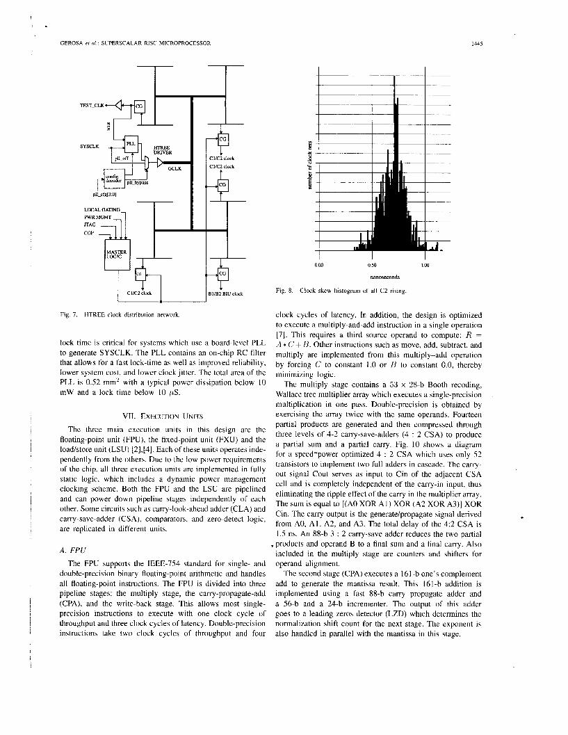
A passive clock distribution network is chosen over a set of distributed clock buffers in order to minimize active power. An HTREE style distribution network (see Fig. 7 ) using metal3 and metal4 produces the best riselfall time performance while maintaining a low total routing capacitance. In addition, skew is minimized among all branches. Grid-like layouts are not considered due to their high routing capacitance. Global clock skew is kept under +/ - 70 pS with this scheme; rise and fall times are under 1.2 nS while average power due to the HTREE driver and the HTREE itself is maintained under 100 mW at 80 MHz.
Since any additional clock skew directly impacts chip cycle time, each regenerator must deliver to the latches the most precise clock possible. The maximum clock line loading on each regenerator is restricted, and several regenerators, each designed to drive a restricted range of load with a predefined delay tolerance, are made available to the chip auto- synthesis tools. The synthesis tools then choose the appropriate regenerator for a given clock line load. A histogram of the rising edge of C2 skew distribution is shown in Fig. 8.
vr. PHASE LOCK LOOP
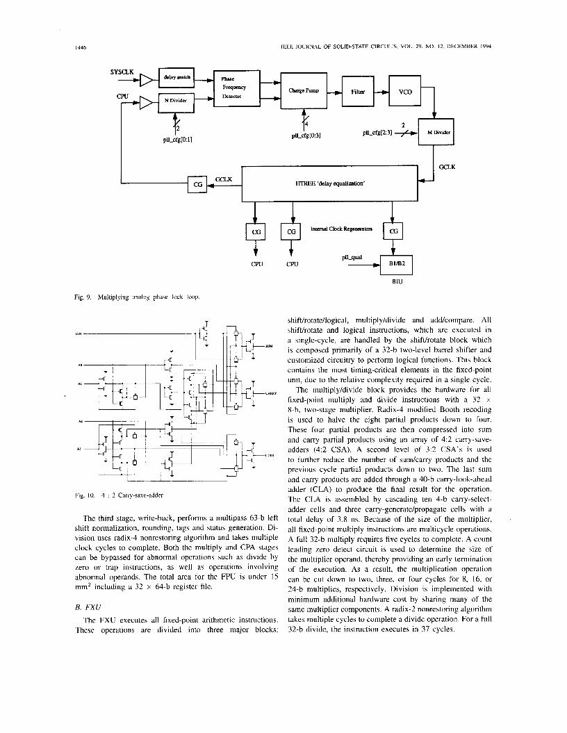
The PLL generates a global clock (GCLK) with a 50 percent duty cycle and low jitter from an external system clock (SYSCLK). The PLL supports SYSCLK frequencies from 16.6 to 100 MHz, and CPU to SYSCLK ratios of 1, 2, 3. and 4. The PLL may be powered down when the processor is in sleep mode, limiting power consumption to transistor leakage only. The major functional blocks for the PLL are shown in Fig. 9 [SI.
A novel dual-divider circuit in the feedback reduces the required bandwidth of the voltage-controlled oscillator (VCO) from 167 MHz to 100 MHz. A programmable charge pump is used in con.junction with two dividers in the feedback path to reduce the variation of damping coefficient and natural frequency. Good control of both these parameters along with
.
I
GEROSA er U[.: SUPERSCALAR RISC MICROPROCESSOR
PWR MGMT JTAG COP
1445
The three main execution units in this design are the floating-point unit (FPU), the fixed-point unit (FXU) and the loadktore unit (LSU) [2],[4]. Each of these units operates inde- pendently from the others. Due to the low power requirements of the chip, all three execution units are implemented in fully static logic, which includes a dynamic power management clocking scheme. Both the FPU and the LSU are pipelined and can power down pipeline stages independently of each other. Some circuits such as carry-look-ahead adder (CLA) and carry-save-adder (CSA), comparators, and zero-detect logic, are replicated in different units.
A. FPU
The FPU supports the IEEE-754 standard for single- and double-precision binary floating-point arithmetic and handles all floating-point instructions. The FPU is divided into three pipeline stages: the multiply stage, the carry-propagate-add
I (CPA), and the write-back stage. This allows most $ingle- precision instructions to execute with one clock cycle of
I I
I throughput and three clock cycles of latency. Double-precision instructions take two clock cycles of throughput and four
partial products are generated and then compressed through three levels of 4-2 carry-save-adders (4 : 2 CSA) to produce a partial sum and a partial carry. Fig. 10 shows a diagram for a speed*power optimized 4 : 2 CSA which uses only 52 transistors to implement two full adders in cascade. The cany- out signal Cout serves as input to Cin of the adjacent CSA cell and is completely independent of the carry-in input, thus eliminating the ripple effect of the carry in the multiplier array. The sum is equal to [(A0 XOR A l ) XOR (A2 XOR A3)j XOR Cin. The carry output is the generatelpropagate signal derived from AO, Al , A2, and A3. The total delay of the 4:2 CSA is 1.5 ns. An 88-b 3 : 2 carry-save adder reduces the two partial
, products and operand B to a final sum and a final carry. Also included in the multiply stage are counters and shifters for operand alignment.
The second stage (CPA) executes a 161 -b one's complement add to generate the mantissa result. This 161-b addition is implemented using a fast 88-b carry propagate adder and a 56-b and a 24-b incrementer. The output of this adder goes to a leading zeros detector (LZD) which determines the normalization shift count for the next stage. The exponent is also handled in parallel with the mantissa in this stage.
I446 IEEE JOURNAL OF SOLID-STATE CIRCUI.‘S, VOL. 29. NO. 12, DECEMBER 1994
t CPU
t CPU
BILI
Fig. 9. Multiplying analog phase lock loop.
Fig. IO. 4 : 2 Carry-savc-adder.
The third stage, write-back, performs a multipass 63-b left shift normalization, rounding, tags and status generation. Di- vision uses radix-4 nonrestoring algorithm and takes multiple clock cycles to complete. Both the multiply and CPA stages can be bypassed for abnormal operations such as divide by zero or trap instructions, as well as operations involving abnormal operands. The total area for the FPU is under 15 mm2 including a 32 x 64-b register file.
B. FXU
The FXU executes all fixed-point arithmetic instructions. These operations are divided into three major blocks:
shift/rotate/logical, multiply/divide and addkompare. All shifthotate and logical instructions, which are executed in a single-cycle, are handled by the shifthotate block which is composed primarily of a 32-b two-level barrel shifter and customized circuitry to perform logical functions. This block contains the most timing-critical elements in the fixed-point unit, due to the relative complexity required in a single cycle.
The multiply/divide block provides the hardware for all fixed-point multiply and divide instructions with a 32 x 8-b. two-stage multiplier. Radix-4 modified Booth recoding is used to halve the eight partial products down to four. These four partial products are then compressed into sum and cany partial products using an array of 4:2 cany-save- adders (4:2 CSA). A second level of 3:2 CSA’s is used to further reduce the number of sumkarry products and the previous cycle partial products down to two. The last sum and carry products are added through a 40-b carry-look-ahead adder (CLA) to produce the final result for the operation. The CLA is assembled by cascading ten 4-b carry-select- adder cells and three carry-generatelpropagate cells with a total delay of 3.8 ns. Because of the size of the multiplier, all fixed-point multiply instructions are multicycle operations. A full 3 2 4 multiply requires five cycles to complete. A count leading zero detect circuit is used to determine the size of the multiplier operand, thereby providing an early termination of the execution. As a result, the multiplication operation can be cut down to two, three, or four cycles for 8, 16, or 2 4 4 multiplies, respectively. Division is implemented with minimum additional hardware cost by sharing many of the same multiplier components. A radix-2 nonrestoring algorithm takes multiple cycles to complete a divide operation. For a full 32-b divide, the instruction executes in 37 cycles.
GEROSA ef U / . : SUPERSCALAR RISC MICROPROCESSOR
The addkompare block is comprised of a 32-b carry-look- ahead adder (CLA), a 32-b comparator, and a zero-detect circuit. All arithmetic and compare instructions are handled by this block and executed in single-cycle. The total area for the fixed-point unit is 4.7 mm2 which includes a 32 x 32 register file.
c. LSU The LSU is the data transfer interface between the cachehus
and the general purpose and floating point registers (GPR and FPR, respectively). The LSU contains a 32-b CLA adder to calculate the effective address for the load or store operation. The same adder that is used in the FXU is also used in the LSU, although the LSU does not use the carry-out or overflow bits produced by the adder. The LSU also includes a 16-b comparator to compare address in the LSU's store queues with address of load instructions that are bypassing the stores. Although only one transfer will occur between the LSU and data cache per cycle, there are two unidirectional (64-b) data buses between the cache and LSU. The time between load data being sent to the LSU and store data being sent to the data cache makes switching a single bus not feasible. Single- and double-precision floating-point loads and stores are also handled by the LSU. The LSU uses zero detect circuitry to determine whether store data needs to be normalized or denormalized. If required, the LSU performs normalization and denormalization of store data, one bit at a time, with a worst-case latency of 23 cycles. The total area for the LSU is just under 7 mm2.
I
VIII. GENERAL PURPOSE REGISTERS
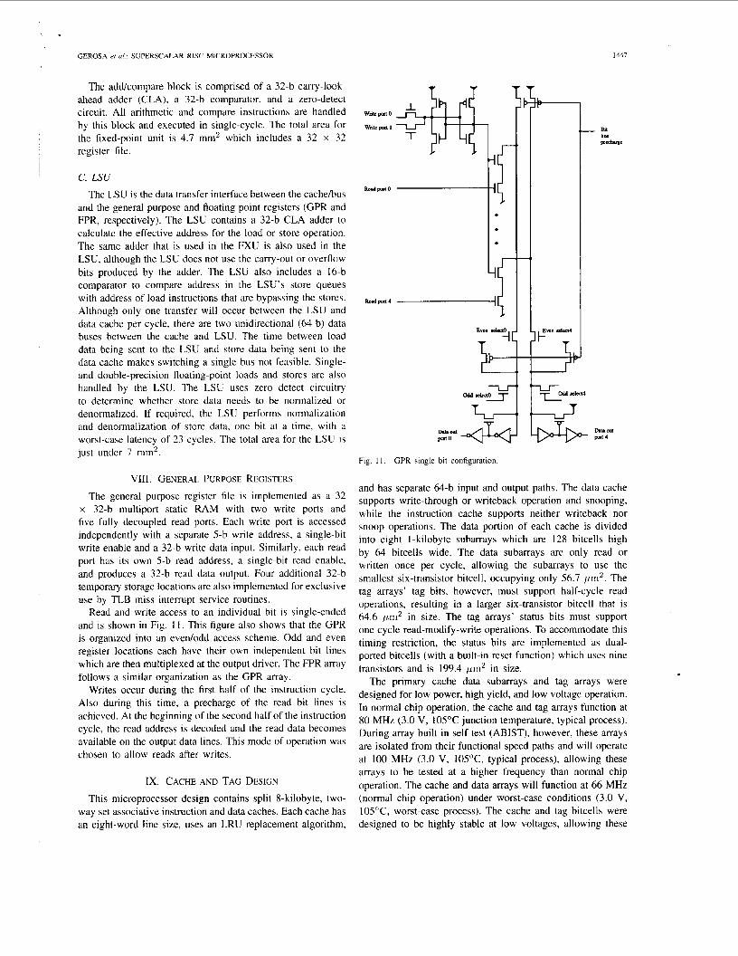
The general purpose register file is implemented as a 32 x 32-b multiport static RAM with two write ports and five fully decoupled read ports. Each write port is accessed independently with a separate 5-b write address, a single-bit write enable and a 32-b write data input. Similarly, each read port has its own 5-b read address, a single-bit read enable, and produces a 32-b read data output. Four additional 32-b temporary storage locations are also implemented for exclusive use by TLB miss interrupt service routines.
Read and write access to an individual bit is single-ended and is shown in Fig. 11 . This figure also shows that the GPR is organized into an even/odd access scheme. Odd and even register locations each have their own independent bit lines which are then multiplexed at the output driver. The FPR array follows a similar organization as the GPR array.
Writes occur during the first half of the instruction cycle. Also during this time, a precharge of the read bit lines is achieved. At the beginning of the second half of the instruction cycle, the read address is decoded and the read data becomes available on the output data lines. This mode of operation was chosen to allow reads after writes.
Ix . CACHE AND TAG DESIGN
This microprocessor design contains split 8-kilobyte, two- way set associative instruction and data caches. Each cache has an eight-word line size, uses an LRU replacement algorithm,
Fig. 11. GPR single bit configuration
144:
- Bit lime
and has separate 64-b input and output paths. The data cache supports write-through or writeback operation and snooping, while the instruction cache supports neither writeback nor snoop operations. The data portion of each cache is divided into eight I-kilobyte subarrays which are 128 bitcells high by 64 bitcells wide. The data subarrays are only read or written once per cycle, allowing the subarrays to use the smallest six-transistor bitcell, occupying only 56.7 pin2. The tag arrays' tag bits, however, must support half-cycle read operations, resulting in a larger six-transistor bitcell that is 64.6 pm2 in size. The tag arrays' status bits must support one cycle read-modify-write operations. To accommodate this timing restriction, the status bits are implemented as dual- ported bitcells (with a built-in reset function) which uses nine transistors and is 199.4 pm2 in size.
The primary cache data subarrays and tag arrays were designed for low power, high yield, and low voltage operation. In normal chip operation, the cache and tag arrays function at 80 MHz (3.0 V, 105°C junction temperature, typical process). During array built in self test (ABIST), however. these arrays are isolated from their functional speed paths and will operate at 100 MHz (3.0 V, 105"C, typical process), allowing these arrays to be tested at a higher frequency than normal chip operation. The cache and data arrays will function at 66 MHz (normal chip operation) under worst-case conditions (3.0 V, 105"C, worst-case process). The cache and tag bitcells were designed to be highly stable at low voltages, allowing these
I448 IEEE JOURNAL OF SOLID-STATE CIRCUITS, VOL. 29, NO. L2. DECEMBER 1994
c2
c1
S n c h WL
TAG WL
cncha SAN
TAG SAN
TAG data out
HITOMTI
WAYSELM
cncha data out
XBLl BLO XBLn BLI
W m I
SENSEI
/ "dtd \
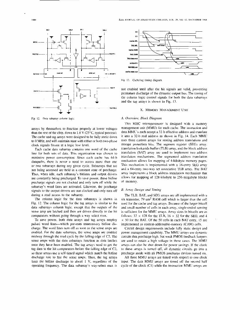
\ ".lid /
Dour not enabled until after the hit signals are valid, preventing premature discharge of the dynamic output bus. The timing of the column logic control signals for both the data subarrays and the tag arrays is shown in Fig. 13.
X. MEMORY MANAGEMENT UNIT
Fig. 12. Data subarray column logic. A. Overview, Block Diagram
arrays by themselves to function properly at lower voltages than the rest of the chip, down to 1.8 V (25"C, typical process). The cache and tag arrays were designed to be fully static down to 0 MHz, and will maintain state with either or both two-phase clock signals frozen at a logic low level.
Each cache data subarray contains one word of the cache line for both sets of data. This organization was chosen to minimize power consumption: Since each cache has 64-b datapaths, there is never a need to access more than one or two subarrays during any given cycle. Subarrays that are not being accessed are held in a constant state of precharge. Thus, when idle, each subarray's bitlines and output drivers are constantly being precharged. To save power, these bitline precharge signals are not clocked and only turn off while the subarray's word lines are activated. Likewise, the precharge signals to the output drivers are not clocked and only turn off during a read access to the subarray.
The column logic for the data subarrays is shown in Fig. 12. The column logic for the tag arrays is similar to the data subarrays column logic, except that the outputs of the sense amp are latched and then are driven directly to the hit comparators without going through a way-select mux.
To save power, both data arrays and tag arrays employ pulsed word lines-which prevents unnecessary bitline dis- charge. The word lines turn off as soon as the sense amps are enabled. For the data subarrays, the sense amps are enabled midway through the read cycle by the falling edge of C2. The sense amps with the data subarrays function as data latches once they have been enabled. The tag arrays need to get the tag data to the hit comparators before the falling edge of C?, so these arrays use a self-timed signal which match the bitline discharge rate to fire the sense amps. Thus, the tag arrays limit the bitline discharge to about 1 V, regardless of the operating frequency. The data subarray's way-select mux is
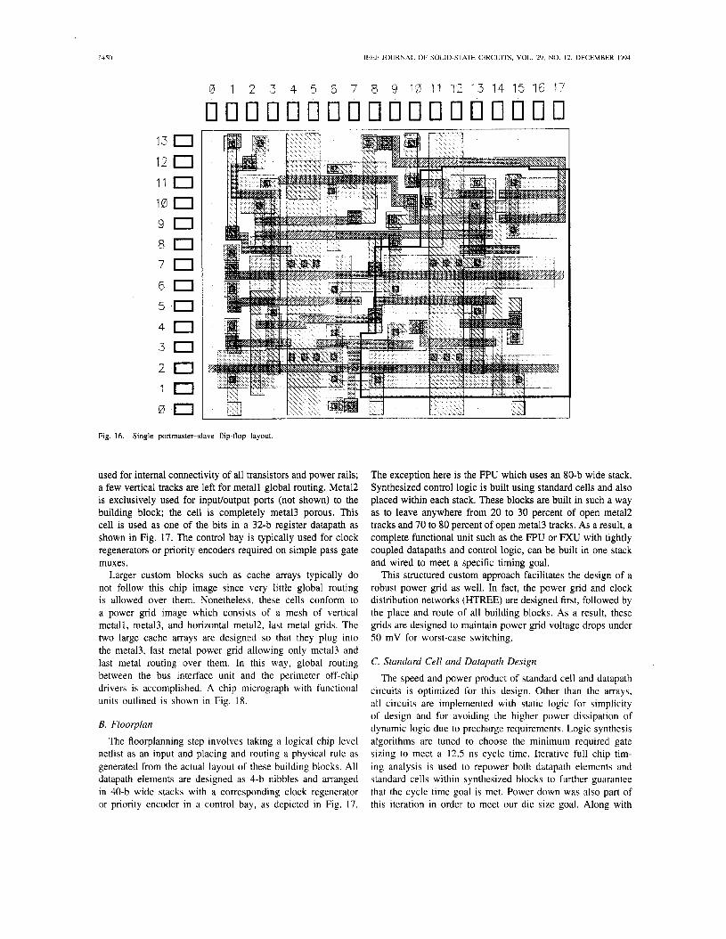
This RISC microprocessor is designed with a memory management unit (MMU) for each cache. The instruction and data MMU's each accept a 32-b effective address and translate it into a 32-b real address as shown in Fig. 14. Each MMU uses three custom arrays for storing address translations and storage protection bits. The segment register (SEG) array, translation lookaside buffer (TLB) array, and the block address translation (BAT) array are used to implement two address translation mechanisms. The segmented address translation mechanism allows for mapping of 4-kilobyte memory pages. This mechanism is implemented with a 16-entry SEG array and a 64-entry two-way set associative TLB array. The BAT array implements a block address translation mechanism that allows for mapping of 128-kilobyte to 256-megabyte blocks of memory.
B. Array Design and Timing
The TLB, BAT, and SEC arrays are all implemented with a six-transistor, 79 um2 RAM cell which is larger than the cell used for the cache and tag arrays. Because of the larger bitcell and small number of cells in each array, single-ended sensing is sufficient for the MMU arrays. Array sizes in bitcells are as follows: 32 x 128 for the TLB, 16 x 32 for the SEG, and 4 x 50 for the BAT. Of the 50 cells in each BAT entry, 15 are implemented as content-addresable-memory (CAM) cells.
Circuit design requirements include fully static design and power management capability. The MMU arrays use dynamic circuits that precharge high, but weak PMOS feedback keepers are used to retain a high voltage in these cases. The MMU arrays can also be shut down for power savings. If the clock to these arrays is turned off, all dynamic circuits go into a precharge mode with all PMOS precharge devices turned on.
All three MMU arrays are timed with respect to one clock input. The data MMU arrays are timed off the second half cycle of the clock (Cl) while the instruction MMU arrays are
GEKOSA er al.: SUPEKSCALAK KlSC .MICKOPKOCESSOK 1449
Segment Registers 16 Entries
Virtual Address
2-way 64 entry
1 2,
4 entries CAM
I
\ /
Real Address T A Real Page Number
Fig. 14. Address translation block diagram.
timed off the first half cycle (C2). When the clock input to the arrays goes low, the bitlines and any other dynamic circuits are precharged. When the clock goes high, the word lines are enabled and the data is read out of the array. Output data from the arrays must be latched on the falling edge of C1 for the data MMU and the falling edge C2 for the instruction MMU.
C. TLB Comparator Circuit
Even though no differential sensing is used in the MMU arrays, dual-ended outputs are provided for other reasons. One example of this is the comparator used between the virtual address and the TLB array outputs (see Fig. 14). Two 36-b dynamic comparators are used, each made up of 36 2-input dynamic XOR gates that feed into a 36-b dynamic NOR function. One bit of the comparator between the SEG and TLB is shown in Fig. 15. This comparator is built into the TLB array with the SEG outputs routed to the TLB.
In order to keep the dynamic NOR gate from falsely discharging, its inputs (node XORO) must not go high until i t is known that the comparison data is stable. This would usually require that one of the inputs arrive at the XOR first or that a qualifying signal exist to gate the inputs. However, exact routing conditions were not known at array design time and there was no timing reference available to qualify the outputs. A self-timed reference signal could have been generated; however, the dynamic XOR gate shown in Fig. 15 eliminates the need for one because it times the comparison off the TLB and SEG data. This XOR uses the fact that all of the outputs from the two RAM arrays w,ill transition from a zero to a one when they evaluate. When the CLK input is low the signal XNOR is precharged high and the bitlines in the arrays are precharged high. When the CLK input is high, the arrays are read by driving their word lines high. causing one of the two bitlines in each array to go low. This will cause
8
XOR
36 pLlldcwns DYNAMIC NOR
10
SEG-WORDLINE
:, w‘ z E 10
A
16 cells tall 1 I
~.____ --I SEGMENT ARRAY
Fig. 15. TLB and SEG read/compare path.
one of the outputs from each array to go high and potentially discharge node XNOR. This node can discharge only when both the TLB and SEG outputs are valid.
XI. PHYSICAL DESIGN
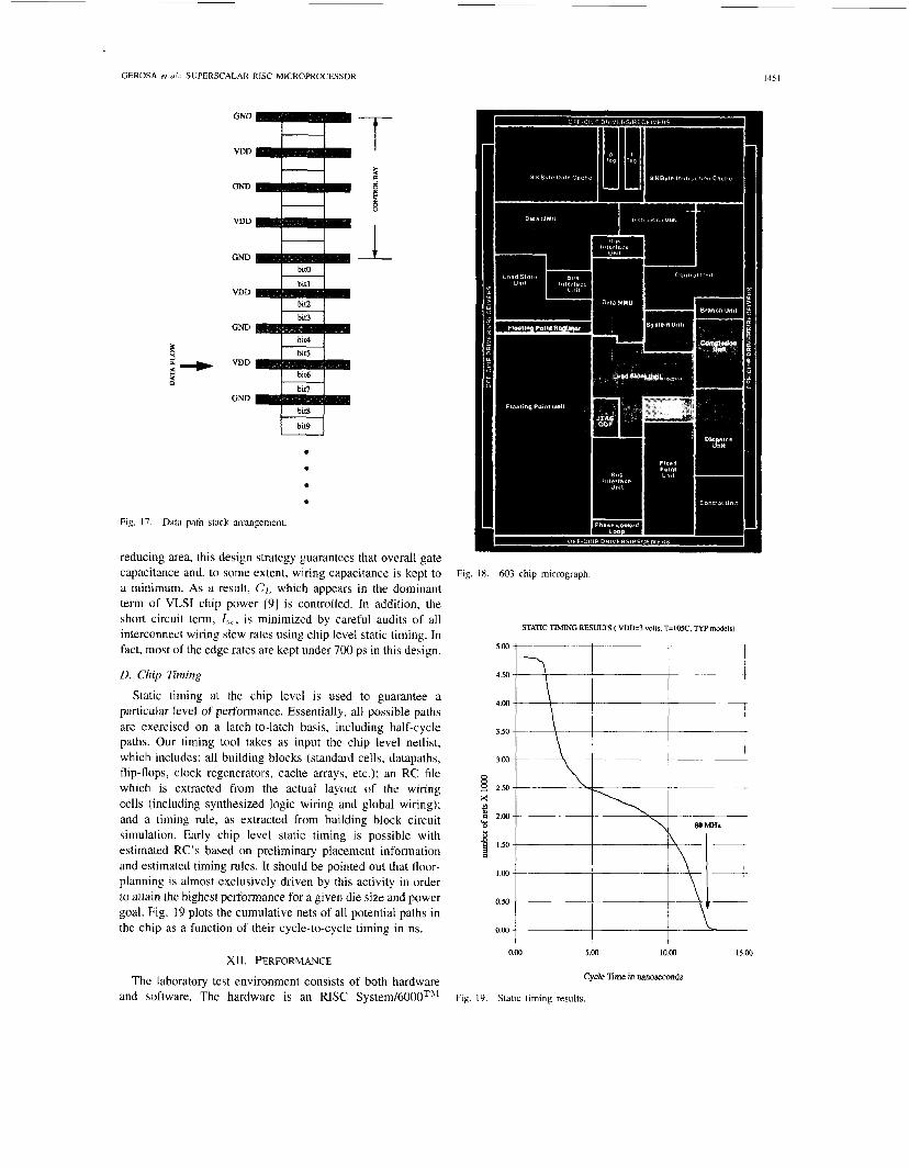
The physical realization of this chip follows what is com- monly referred to as structured custom VLSI design. Essen- tially, design libraries which contain standard cells used in synthesized logic, custom blocks used in datapaths, and larger custom blocks such as phase-lock-loops and off chip drivers are built following a specific chip ‘image’ as exemplified by the layout in Fig. 16. These custom building blocks are then floorplanned, powered, and globally wired in a stack orientation typically 40 b wide, as shown in Fig. 17. For example, datapath timing-driven placement can be done with a granularity of a 4-b nibble. As a result, the same tools used for standard cell place and route are used to assemble complex datapaths [8].
A. Chip Image
The layout of the standard cells and datapath elements is such that metal1 is only used within the building block itself, while most of metal2 and metal3 tracks are reserved for global routing and power grids. Essentially, these building blocks are metall, metal2, and metal3 ‘porous.’ Fig. 16 illustrates the layout of a master-slave flip-flop cell. Polysilicon gates go in the horizontal direction for the most part; metal1 is mostly
1450 IEEE JOURNAL OF SOLID-STATE CIRCUITS, VOL. 29, NO. I ? , DECEMBER 1994
Fig. 16. Single portmaster-slave flip-flop layout.
used for internal connectivity of all transistors and power rails; a few vertical tracks are left for metal1 global routing. Metal2 is exclusively used for input/output ports (not shown) to the building block; the cell is completely metal3 porous. This cell is used as one of the bits in a 32-b register datapath as shown in Fig. 17. The control bay is typically used for clock regenerators or priority encoders required on simple pass gate muxes.
Larger custom blocks such as cache arrays typically do not follow this chip image since very little global routing is allowed over them. Nonetheless, these cells conform to a power grid image which consists of a mesh of vertical metall, metal3, and horizontal metal2, last metal grids. The two large cache arrays are designed so that they plug into the metal3, last metal power grid allowing only metal3 and last metal routing over them. In this way, global routing between the bus interface unit and the perimeter off-chip drivers is accomplished. A chip micrograph with functional units outlined is shown in Fig. 18.
B. Floorplan
The floorplanning step involves taking a logical chip level netlist as an input and placing and routing a physical rule as generated from the actual layout of these building blocks. All datapath elements are designed as 4-b nibbles and arranged in 40-b wide stacks with a corresponding clock regenerator or priority encoder in a control bay, as depicted in Fig. 17.
The exception here is the FPU which uses an 80-b wide stack. Synthesized control logic is built using standard cells and also placed within each stack. These blocks are built in such a way as to leave anywhere from 20 to 30 percent of open metal2 tracks and 70 to 80 percent of open metal3 tracks. As a result, a complete functional unit such as the FPU or FXU with tightly coupled datapaths and control logic, can be built in one stack and wired to meet a specific timing goal.
This structured custom approach facilitates the design of a robust power grid as well. In fact, the power grid and clock distribution networks (HTREE) are designed first, followed by the place and route of all building blocks. As a result, these grids are designed to maintain power grid voltage drops under SO mV for worst-case switching.
C. Standard Cell and Datapath Design
The speed and power product of standard cell and datapath circuits is optimized for this design. Other than the arrays, all circuits are implemented with static logic for simplicity of design and for avoiding the higher power dissipation of dynamic logic due to precharge requirements. Logic synthesis algorithms are tuned to choose the minimum required gate sizing to meet a 12.5 ns cycle time. Iterative full chip tim- ing analysis is used to repower both datapath elements and standard cells within synthesized blocks to further guarantee that the cycle time goal is met. Power down was also part of this iteration in order to meet our die size goal. Along with
GEROSA et al.: SUPERSCALAR RlSC MICROPROCESSOR 1451
GND
VDD
H GND
H VDD
GND
VDD
GND
k VDD
GND
0
0
0
0
Fig. 17. Data path stack arrangement
reducing area, this design strategy guarantees
T
i
that overall gate capacitance and, to some extent, wiring capacitance is kept to a minimum. As a result, CL which appears in the dominant term of VLSI chip power [9] is controlled. In addition, the
Fig. 18. 603 chip micrograph.
STATlC TJhfINCi RESULTS ( VDD=3 volts, T=lOSC. TYP models) short circuit term, Isc , is minimized by careful audits of all interconnect wiring slew rates using chip level static timing. In fact, most of the edge rates are kept under 700 ps in this design.
D. Chip Timing
Static timing at the chip level is used to guarantee a particular level of performance. Essentially, all possible paths are exercised on a latch-to-latch basis, including half-cycle paths. Our timing tool takes as input the chip level netlist, which includes: all building blocks (standard cells, datapaths, flip-flops, clock regenerators, cache arrays, etc.); an RC file which is extracted from the actual layout of the wiring cells (including synthesized logic wiring and global wiring); and a timing rule, as extracted from building block circuit simulation. Early chip level static timing is possible with estimated RC’s based on preliminary placement information and estimated timing rules. It should be pointed out that floor- planning is almost exclusively driven by this activity in order to attain the highest performance for a given die size and power goal. Fig. 19 plots the cumulative nets of all potential paths in the chip as a function of their cycle-to-cycle timing in ns.
0.00 5.00 10.00 15.00
Cycle lime in nanoseconds XII. PERFORMANCE
The laboratory test environment consists of both hardware and software. The hardware is an RISC Systetn/6000T’* Fig. 19. Static timing results.
1352
Processor Frequency in MHz
3 . 8 0 3 . 7 0 3 . 6 0 3 . 5 0 3 . 4 0
3 3.30 - 3 . 1 0
9 2 . 9 0 2 . 8 0 2 . 7 0 2 .60 2 .50
h - g 3 . 2 0
n 3.00
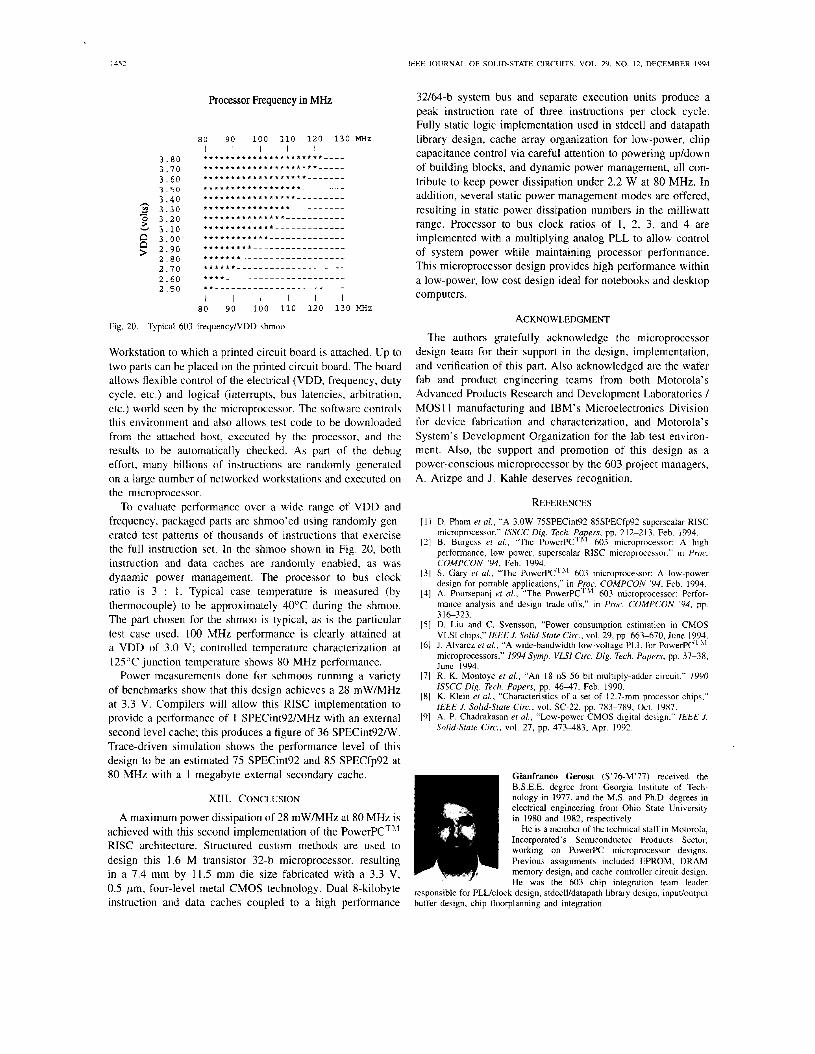
Fig. 20. Typical 603 frequencyNDD shmoo
Workstation to which a printed circuit board is attached. Up to two parts can be placed on the printed circuit board. The board allows flexible control of the electrical (VDD, frequency, duty cycle, etc.) and logical (interrupts, bus latencies, arbitration, etc.) world seen by the microprocessor. The software controls this environment and also allows test code to be downloaded from the attached host, executed by the processor, and the results to be automatically checked. As part of the debug effort, many billions of instructions are randomly generated on a large number of networked workstations and executed on the microprocessor.
To evaluate performance over a wide range of VDD and frequency, packaged parts are shmoo’ed using randomly gen- erated test patterns of thousands of instructions that exercise the full instruction set. In the shmoo shown in Fig. 20, both instruction and data caches are randomly enabled, as was dynamic power management. The processor to bus clock ratio is 3 : 1 . Typical case temperature is measured (by thermocouple) to be approximately 4OoC during the shmoo. The part chosen for the shmoo is typical, as is the particular test case used. 100 MHz performance is clearly attained at a VDD of 3.0 V; controlled temperature characterization at 125°C junction temperature shows 80 MHz performance.
Power measurements done for schmoos running a variety of benchmarks show that this design achieves a 28 mW/MHz at 3.3 V. Compilers will allow this RISC implementation to provide a performance of 1 SPECint92MHz with an external second level cache; this produces a figure of 36 SPECint92N. Trace-driven simulation shows the performance level of this design to be an estimated 75 SPECint92 and 85 SPECfp92 at 80 MHz with a I megabyte external secondary cache.
XIII. CONCLUSION
A maximum power dissipation of 28 mW/MHz at 80 MHz is achieved with this second implementation of the PowerPCThl RISC architecture. Structured custom methods are used to design this 1.6 M transistor 32-b microprocessor, resulting in a 7.4 mm by 11.5 mm die size fabricated with a 3.3 V, 0.5 pm, four-level metal CMOS technology. Dual 8-kilobyte instruction and data caches coupled to a high performance
IEEE JOURNAL OF SOLID-STATE CIRCUITS, VOL. 29, NO. 12. DECEMBER 1994
32164-b system bus and separate execution units produce a peak instruction rate of three instructions per clock cycle. Fully static logic implementation used in stdcell and datapath library design, cache array organization for low-power, chip capacitance control via careful attention to powering up/down of building blocks, and dynamic power management, all con- tribute to keep power dissipation under 2.2 W at 80 MHz. In addition, several static power management modes are offered, resulting in static power dissipation numbers in the milliwatt range. Processor to bus clock ratios of 1, 2, 3, and 4 are implemented with a multiplying analog PLL to allow control of system power while maintaining processor performance. This microprocessor design provides high performance within a low-power, low cost design ideal for notebooks and desktop computers.
ACKNOWLEDGMENT
The authors gratefully acknowledge the microprocessor design team for their support in the design, implementation, and verification of this part. Also acknowledged are the wafer fab and product engineering teams from both Motorola’s Advanced Products Research and Development Laboratories I MOS 1 1 manufacturing and IBM’s Microelectronics Division for device fabrication and characterization, and Motorola’s System’s Development Organization for the lab test environ- ment. Also, the support and promotion of this design as a power-conscious microprocessor by the 603 project managers, A. Arizpe and J. Kahle deserves recognition.
REFERENCES
D. Pham et al., “A 3.0W 7SSPECint92 8SSPECfp92 superscalar RISC microprocessor,” ISSCC Dig. Tech. Papers, pp. 21 2-21 3. Feb. 1994. B. Burgess et al., “The PowerPCTh’ 603 microprocessor: A high performance, low power, superscalar RISC microprocessor,” in Proc. COMPCON ‘94, Feb. 1994. S. Gary et al., “The PowerPCT“ 603 microprocessor: A low-power design for portable applications,” in Proc. COMPCON ’Y4, Feb. 1994. A. Poursepanj et al., “The PowerPC’” 603 microprocessor: Perfor- tnance analysis and design trade-offs,” in Proc. COMPCON ’94, pp. 316323. D. Liu and C. Svensson, “Power consumption estimation in CMOS VLSI chips,” IEEE J. Solid-Sfate Circ., vol. 29, pp. 663-670, June 1994. J. Alvarez et al., “A wide-bandwidth low-voltage PLL for PowerPC’ ‘I microprocessors,” 1994 Symp. VLSI Circ. Dig. Tech. Papers. pp. 37-38, June 1994. R. K. Montoye et al., “An 18 nS 56 bit multiply-adder circuit,” 1990 ISSCC Dig. Tech. Papers, pp. 4 6 4 7 , Feb. 1990. K. Klein et GI. , “Characteristics o f a set of 12.7-mm processor chips,” IEEE J . Solid-State Circ., vol. SC-22, pp. 783-789, Oct. 1987. A. P. Chadrakasan et al., “Low-power CMOS digital design.” IEEE J . Solid-State Circ., vol. 27, pp. 473483, Apr. 1992.
Gianfranco Gerosa (S’76-M’77) received the B.S.E.E. degree from Georgia Institute of Tech- nology in 1977, and the M.S. and Ph.D. degrees in electrical engineering from Ohio State University in 1980 and 1982, respectively.
He is a member of the technical staff in Motorola, Incorporated’s Semiconductor Products Sector, working on PowerPC microprocessor designs. Previous assignments included EPROM, DRAM memory design, and cache controller circuit design. He was the 603 chip integration team leader
responsible for PLWclock design. stdceWdatapath library design, inpudoutput buffer design, chip floorplanning and integration.
GEROSA el < I / . : SLIPERSCALAR RISC MICROPROCESSOR 1453
Sonya Gary received the B.S. degree in electrical and computer engineering from the University of Texas in 1989.
She is a design engineer for Motorola, Incorpo- rated, at the Somerset Design Center in Au$tin, TX, and is currently responsible for power management on a PowerPC portable microprocessor design. As a member of the PowerPC 603 design team, she was the lead designer for instruction completion, excep- tion handling, and internal pouer management. Prior to this, she held Dositions as a design engineer on
Jose Alvarez (M'85) received the B.S.E.E degree in 1985 from Tulane University, and the M.S.E.E. degree in 1989 from Southern Methodist University. He worked toward the Ph.D. degree at the Univer- sity of Texas, Arlington.
From 1985 to 1988 he worked in the RADAR Division of Texas Instruments, designing analog servo systems for the LANTIRN terrain following RADAR. From 1988 to 1992, he worked in the Linear division of Texas Instruments. where he de- signed BiCMOS analog and digital cells for mixed
the MC88410 secondary cache controller chip and the Engineering Rotational Program for Motorola's Semiconductor Products Sector. Her research interests include power estimation and reduction techniques for IC's and architecting low-power microprocessors.
signal IC'% In 1992, he joined the RISC division of Motorola, where he is currently a Principal Design Engineer responsible for phase-locked loop design and clocking for various PowerPC microprocessors.
Carl Dietz received the B.S. degree in computer and electrical engineering from Purdue University in 1989.
He is a custom circuit designer for IBM at the Somerset Design Center in Austin, TX, where he is primarily involved in cache array design for PowerPC microproces\ors for portable applications. Previously, he held a position in cache design for the 29000 group at Advanced Micro Device?. His research interests include high-speed, low-power custom array design. cache organization, and com- puter architecture.
Dac Pham received the R.S. degree in computer electronics engineering from the University of Rhode Island in 1986, and the M.S. degree in electrical engineering from Rensselaer Polytechnic Institute in 1987. He is currently working toward the Ph.D. degree in materials science at the University of Vermont.
In 1987, he joined IBM in Burlington, VT. where he has been associated with the Industry Standard Microprocessor Development group. working on IBM's 386SLC. 486SLC2. and Blue Lightning - -
microprocessors. He is currently managing the custom circuits and integration team for Portable PowerPC microprocessors design at Somerset Design Center, a joint effort of IBM, Motorola, and Apple. His principal interests are in the areas of custom circuit design, tools development, and microprocessor physical design and integratlon.
interests include low-p, CAD tools.
Hector Sanchez received the B.S. and M.E. degrees i n electrical engineering, in 1987 and 1990, respec- tively, from Texas A&M University.
He is a circuit design engineer with Motorola, working on the development of microprocessors for portable applications at the Somerset Design Center in Austin, TX. His professional interests include phase-locked loop circuit design, clock generation, clock distribution, high-speed analog/digital circuits, and microprocessor chip integration.
Pete lppolito received the B.S.E.E. degree from Princeton University, Princeton, NJ in 1980. and the M.S.E.E. degree from the University of California, Los Angeles, in 1983.
He is currently employed by IBM at the Somerset Design Center in Austin, TX, where he is involved primarily with circuit design issues for the PowerPC 603 microprocessor. He was previously with the IBM General Technology Division in East Fishkill, NY, where he wa5 involved in the design and development of bipolar custom IC's.
Tai Ngo received the B.S.E.E. and M.S.E.E. degrees from Texas A&M University, in 1979 and 1981, respectively.
He is a CMOS circuit design engineer with IBM, working on PowerPC microprocessor designs. He was involved in circuit design for the PowerPC 603 Execution Unit and cell library development.
Kathy Hoover received the B.S. and M.S. degrees in electrical engineering from the University of Michigan, in 1990 and 1992, respectively.
In 1992, she began working for IBM Corporation in Austin, TX, as a VLSI circuit designer. She designed the custom memory management arrays for the PowerPC 603 which include the TLB, BAT, and Segment Registers. Currently, she is working on cache and memory management array circuit de- signs. She has also been involved in RISC memory management architectural issues. Her professional
ower CMOS circuit design and custom circuit design
Suzanne Litch (PM'93) received the B.S. degree in electrical engineering from Rice University, Hous- ton, TX, in 1989.
Upon graduation she joined Motorola Incorpo- rated, Austin, TX, where she worked on the En- gineering Rotational Program and then in RISC Customer Applications, until she joined the Som- erset Design Center in 1992. She has contributed to the microarchitecture and design of the PowerPC 603 microprocessor, specifically in the loadlstore area.
1454 Ik.EI JOURNAL OF SOLID-STATE CIRCUITS, VOL. 29. NO. 12, DECEMBER 1994
Jim Eno receivcd the B.S.E.E. degree from North Carolina Stale University in 1989.
He i \ employed as a senior engineer at Digital Equipment Corporation’s Research and Design Center, Austin, TX. Before his employment with DEC. he was with the Somerset Design Center in Austin, working on the microarchitectcre and design of the PowerPC 603 microprocessor. Previous to this, Eno was involved in ASIC design support and tool devclopment at Compaq Computer Corporation. His research interests include low-power microprocessor design and the propagation of acoustic waves in various materials, as enhanced by interaction with selected organic compounds.
James Golab (M’81) received the B.S. and M.Eng. degrees in applied and engineering physics from Cornell Univerrity, in 1980 and 198 I , respectively.
He then joined Motorola Incorporated, Austin, TX, and worked on fast SRAMS until 1986. Since then. he has been involved in the circuit design of embedded arrays and cache control logic design in the RISC microprocessor division.
o n RISC microprocessor Mr. Kahle has numc
processors.
Neil Vanderschaaf (M’78) received the B.S. degree in electrical engineering from Southern Methodist University in 1978, and the M.S. degree in electncal engineering from Purdue University in 1984. He also received the B.A. degree in music from the University of Iowa in 1976.
He is currently employed by IBM Corporation, Austin, TX, as an advisory engineer. His interests include CMOS circuit design, library management, and circuit simulation techniques.
Jim Kahle received a B.S. degree in electrical engineering from Rice University in 1983.
He is the 603 project co-manager, responsible for portable processor designs in the Somerset facility for the IBM RISC Systed6000 Divihion. He is also responsible for the PowerPC architecture for chips designed in the Somerset Design Center. He was involved in new RISC superscalar designs and in managing POWER2 definition. He implemented the load/store, exception, and processor \ynchronization logic on the POWER chip set. He has been working
. development in Austin since 1983. :rous patents and technical publicaLions on RISC
Related Documents