Abstract— This paper presents a 20 Gb/s injection-locked clock and data recovery circuit for burst-mode applications. Using a new injection-locked LC oscillator as a half rate CDR, relaxes the speed requirements of VCO and re-timing flip flops. This allows us to design higher speed CDR with lower power consumption. Complementary clocks drive two flip flops in the decision circuit for re-timing the data. Simulated in 0.18 μm CMOS, the circuit consumes 68.7 mW at 20 Gb/s, while the recovered clock rms jitter is 0.84 ps, rms in response to a 2 7 -1 PRBS. Keywords— burst mode, clock and data recovery (CDR), fast acquisition CDR, injection locking, injection-locked LC oscillator I. INTRODUCTION lock and data recovery circuits (CDR) are widely used in modern high speed serial link communications where a data stream is transmitted without any additional timing reference. Therefore clock should be extracted from the data to reach synchronous data processing in the receiver. In high- speed optical multi-access network applications such as passive optical networks (PON), amplitude and phase of packets are not fixed and may vary from one packet to another [1]. Therefore, burst-mode receivers must realign clock phase at beginning of every packet and as a result they require fast response time to improve detection of short packets or burst data [2].The clock and data recovery circuit in these receivers extracts a clock from the header area of the burst packets in a small fraction of a packet transmission time [3]. The clock and data recovery circuits can be implemented as open or closed loop circuits. Closed loop CDRs usually use PLL architecture to track the data phase. While closed loop CDRs offer a great performance in the presence of frequency offset and can also suppress the jitter, (Jitter suppression has been achieved by using low bandwidth loop filters in PLL- based CDRs) It leads to long lock time which disqualified them to be used in burst mode data recovery. Since open loop CDRs can achieve fast locking, they are attractive solutions for burst mode data communications. However, open loop CDRs suffer from limited frequency tracking and very weak jitter suppression [4]. Since no repeater is required in these N. Modir, S. Sheikhaei, B. Foroozande, and Elias Soleiman are with the School of Electrical and Computer Engineering, University of Tehhran, Tehran, Iran (e-mail: [email protected]). applications, jitter transfer is not a serious issue [5] and open loop CDRs are proper solution for such applications. Open loop CDRs can be designed by Gated Voltage Control Oscillator (GVCO) or Injection-Locked LC oscillator (ILO). GVCO is used in [5]-[7] for burst mode applications. CDR circuits using GVCOs consume low power and have compact structures. However, ring structure of the GVCOs which is shown in Fig.1 will raise jitter in extracted clock. Also, the operating frequency of GVCOs is lower than ILO [8]. In injection locking method LC VCO is used instead of ring oscillator. It has better phase noise and higher speed in comparison to ring oscillator. A CDR circuit based on injection locking technique is described in [8], in which rise and fall edges of received data has been detected with an edge detector and then injected to an LC oscillator, so it extracts a full rate clock from the input data. However, using injection-locked oscillator as a full rate CDR in the foregoing technique leads to design a high frequency VCOs. Another issue is design of edge detector which needs high speed CML XOR and delay cell circuits. In [9] a half rate injection-locked CDR is described. In this method the injection signal is applied to a super-harmonic ILO. In a super-harmonic structure the only block which operates at twice of the oscillator frequency is edge detector. Therefore, design of edge detector is serious bottleneck in high speed CDR design. Also, these blocks increase power consumption and area of the chip. Din CKout Fig. 1 Gated voltage control oscillator (GVCO) In this paper, a high speed injection-locked CDR circuit has been proposed with a new injection technique. This new architecture improves the speed performance of injection- locked CDR circuit by eliminating edge detector and sampling data with a half rate clock. Since in this new injection technique the output frequency of the oscillator is half of the bit rate, the VCO and the decision circuit operation frequencies are reduced to half of the corresponding value in full rate techniques. In [8] long runs cause fluctuations in VCO 1 output amplitude due to steering unbalanced currents in oscillator A 20 Gb/s Fast Acquisition Clock and Data Recovery Circuit in 0.18 μm CMOS Naeeme Modir, Samad Sheikhaei, Behjat Foroozande, Elias Soleiman C INTERNATIONAL JOURNAL OF CIRCUITS, SYSTEMS AND SIGNAL PROCESSING Issue 4, Volume 7, 2013 240

Welcome message from author
This document is posted to help you gain knowledge. Please leave a comment to let me know what you think about it! Share it to your friends and learn new things together.
Transcript

Abstract— This paper presents a 20 Gb/s injection-locked clock
and data recovery circuit for burst-mode applications. Using a new injection-locked LC oscillator as a half rate CDR, relaxes the speed requirements of VCO and re-timing flip flops. This allows us to design higher speed CDR with lower power consumption. Complementary clocks drive two flip flops in the decision circuit for re-timing the data. Simulated in 0.18 µm CMOS, the circuit consumes 68.7 mW at 20 Gb/s, while the recovered clock rms jitter is 0.84 ps, rms in response to a 27-1 PRBS.
Keywords— burst mode, clock and data recovery (CDR), fast acquisition CDR, injection locking, injection-locked LC oscillator
I. INTRODUCTION lock and data recovery circuits (CDR) are widely used in modern high speed serial link communications where a
data stream is transmitted without any additional timing reference. Therefore clock should be extracted from the data to reach synchronous data processing in the receiver. In high-speed optical multi-access network applications such as passive optical networks (PON), amplitude and phase of packets are not fixed and may vary from one packet to another [1]. Therefore, burst-mode receivers must realign clock phase at beginning of every packet and as a result they require fast response time to improve detection of short packets or burst data [2].The clock and data recovery circuit in these receivers extracts a clock from the header area of the burst packets in a small fraction of a packet transmission time [3].
The clock and data recovery circuits can be implemented as open or closed loop circuits. Closed loop CDRs usually use PLL architecture to track the data phase. While closed loop CDRs offer a great performance in the presence of frequency offset and can also suppress the jitter, (Jitter suppression has been achieved by using low bandwidth loop filters in PLL-based CDRs) It leads to long lock time which disqualified them to be used in burst mode data recovery. Since open loop CDRs can achieve fast locking, they are attractive solutions for burst mode data communications. However, open loop CDRs suffer from limited frequency tracking and very weak jitter suppression [4]. Since no repeater is required in these
N. Modir, S. Sheikhaei, B. Foroozande, and Elias Soleiman are with the
School of Electrical and Computer Engineering, University of Tehhran, Tehran, Iran (e-mail: [email protected]).
applications, jitter transfer is not a serious issue [5] and open loop CDRs are proper solution for such applications.
Open loop CDRs can be designed by Gated Voltage Control Oscillator (GVCO) or Injection-Locked LC oscillator (ILO). GVCO is used in [5]-[7] for burst mode applications. CDR circuits using GVCOs consume low power and have compact structures. However, ring structure of the GVCOs which is shown in Fig.1 will raise jitter in extracted clock. Also, the operating frequency of GVCOs is lower than ILO [8]. In injection locking method LC VCO is used instead of ring oscillator. It has better phase noise and higher speed in comparison to ring oscillator.
A CDR circuit based on injection locking technique is described in [8], in which rise and fall edges of received data has been detected with an edge detector and then injected to an LC oscillator, so it extracts a full rate clock from the input data. However, using injection-locked oscillator as a full rate CDR in the foregoing technique leads to design a high frequency VCOs. Another issue is design of edge detector which needs high speed CML XOR and delay cell circuits. In [9] a half rate injection-locked CDR is described. In this method the injection signal is applied to a super-harmonic ILO. In a super-harmonic structure the only block which operates at twice of the oscillator frequency is edge detector. Therefore, design of edge detector is serious bottleneck in high speed CDR design. Also, these blocks increase power consumption and area of the chip.
Din
CKout
Fig. 1 Gated voltage control oscillator (GVCO)
In this paper, a high speed injection-locked CDR circuit has been proposed with a new injection technique. This new architecture improves the speed performance of injection-locked CDR circuit by eliminating edge detector and sampling data with a half rate clock. Since in this new injection technique the output frequency of the oscillator is half of the bit rate, the VCO and the decision circuit operation frequencies are reduced to half of the corresponding value in full rate techniques.
In [8] long runs cause fluctuations in VCO1 output amplitude due to steering unbalanced currents in oscillator
A 20 Gb/s Fast Acquisition Clock and Data Recovery Circuit in 0.18 µm CMOS
Naeeme Modir, Samad Sheikhaei, Behjat Foroozande, Elias Soleiman
C
INTERNATIONAL JOURNAL OF CIRCUITS, SYSTEMS AND SIGNAL PROCESSING
Issue 4, Volume 7, 2013 240
outputs. So to purify the clock, output of VCO1 is injected to another identical VCO. However, in our proposed CDR there is no steering current in long runs. Therefore, the output clock does not suffer from fluctuations.
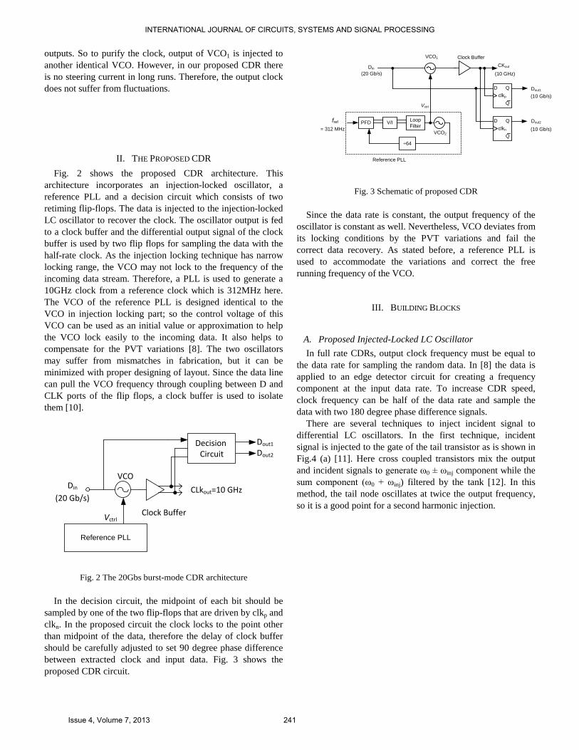
II. THE PROPOSED CDR Fig. 2 shows the proposed CDR architecture. This
architecture incorporates an injection-locked oscillator, a reference PLL and a decision circuit which consists of two retiming flip-flops. The data is injected to the injection-locked LC oscillator to recover the clock. The oscillator output is fed to a clock buffer and the differential output signal of the clock buffer is used by two flip flops for sampling the data with the half-rate clock. As the injection locking technique has narrow locking range, the VCO may not lock to the frequency of the incoming data stream. Therefore, a PLL is used to generate a 10GHz clock from a reference clock which is 312MHz here. The VCO of the reference PLL is designed identical to the VCO in injection locking part; so the control voltage of this VCO can be used as an initial value or approximation to help the VCO lock easily to the incoming data. It also helps to compensate for the PVT variations [8]. The two oscillators may suffer from mismatches in fabrication, but it can be minimized with proper designing of layout. Since the data line can pull the VCO frequency through coupling between D and CLK ports of the flip flops, a clock buffer is used to isolate them [10].
Clock Buffer
Din
(20 Gb/s)
Dout2
Dout1
CLkout=10 GHz
VCO
Vctrl
Reference PLL
Decision Circuit
Fig. 2 The 20Gbs burst-mode CDR architecture
In the decision circuit, the midpoint of each bit should be sampled by one of the two flip-flops that are driven by clkp and clkn. In the proposed circuit the clock locks to the point other than midpoint of the data, therefore the delay of clock buffer should be carefully adjusted to set 90 degree phase difference between extracted clock and input data. Fig. 3 shows the proposed CDR circuit.
PFD V/I LoopFilter
÷64
Reference PLL
VCO1
fref
= 312 MHz
Vctrl
VCO2
Clock Buffer
Din
(20 Gb/s) (10 GHz)
CKout
Dout1D Q
Q
D Q
Q
Dout2
(10 Gb/s)
(10 Gb/s)clkn
clkp
Fig. 3 Schematic of proposed CDR
Since the data rate is constant, the output frequency of the oscillator is constant as well. Nevertheless, VCO deviates from its locking conditions by the PVT variations and fail the correct data recovery. As stated before, a reference PLL is used to accommodate the variations and correct the free running frequency of the VCO.
III. 2BBUILDING BLOCKS
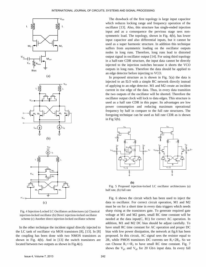
A. 5BProposed Injected-Locked LC Oscillator In full rate CDRs, output clock frequency must be equal to
the data rate for sampling the random data. In [8] the data is applied to an edge detector circuit for creating a frequency component at the input data rate. To increase CDR speed, clock frequency can be half of the data rate and sample the data with two 180 degree phase difference signals.
There are several techniques to inject incident signal to differential LC oscillators. In the first technique, incident signal is injected to the gate of the tail transistor as is shown in Fig.4 (a) [11]. Here cross coupled transistors mix the output and incident signals to generate ω0 ± ωinj component while the sum component (ω0 + ωinj) filtered by the tank [12]. In this method, the tail node oscillates at twice the output frequency, so it is a good point for a second harmonic injection.
INTERNATIONAL JOURNAL OF CIRCUITS, SYSTEMS AND SIGNAL PROCESSING
Issue 4, Volume 7, 2013 241
VDD
LL
M1M2
Bias
RbiasCin
Mtail
Vinj
(a)
VDD
LL
M1M2 M3M4
Iosc
Vctrl
Iinj
Vinj
(b)
VDD
LL
M1M2
M3
M4
IB
V'ctrl
Vinj
(c)
Fig. 4 Injection-Locked LC Oscillators architectures (a) Classical injection-locked oscillator (b) Direct injection-locked oscillator
scheme (c) Another direct injection-locked oscillator scheme
In the other technique the incident signal directly injected to the LC tank of oscillator via MOS transistors [8], [13]. In [8] the coupling has been done with two NMOS transistors as shown in Fig. 4(b). And in [13] the switch transistors are located between two outputs as shown in Fig.4(c).
The drawback of the first topology is large input capacitor which reduces locking range and frequency operation of the oscillator [13]. Also, this structure has single-ended injection input and as a consequence the pervious stage sees non-symmetric load. The topology, shown in Fig. 4(b), has lower input capacitor and also differential inputs, but it cannot be used as a super harmonic structure. In addition this technique suffers from asymmetric loading on the oscillator outputs nodes in long runs. Therefore, long runs lead to distorted output signal in oscillator output [14]. For using third topology in a half-rate CDR structure, the input data cannot be directly injected to the injection switches because it shorts the VCO outputs in long runs. Therefore the data should be applied to an edge detector before injecting to VCO.
In proposed structure as is shown in Fig. 5(a) the data is injected to an ILO with a simple RC network directly instead of applying to an edge detector. M1 and M2 create an incident current in rise edge of the data. Thus, in every data transition the two outputs of the oscillator will be shorted. Therefore the oscillator output clock will lock to data edges. This structure is used as a half rate CDR in this paper. Its advantages are low power consumption and reducing maximum operational frequency by half in compare to the full rate structures. The foregoing technique can be used as full rate CDR as is shown in Fig 5(b).
VDD
LL
M1M2
IB
Vctrl
VDDVDD
Din+ Din-
VDD
LL
M1M2
IB
Vctrl
VDD VDD
Din+ Din-M3
M4
(b) Fig. 5 Proposed injection-locked LC oscillator architectures (a)
half rate, (b) full rate Fig. 6 shows the circuit which has been used to inject the
data to oscillator. For correct circuit operation, M1 and M2 must be on for a short time in every data triggers which needs sharp rising at the transistors gate. To generate required gate voltage at M1 and M2 gates, small RC time constant will be needed at the data input(C, R1) for correct AC operation. In addition, M1 and M2 DC bias should be adjust carefully. To have small RC time constant for AC operation and proper DC bias with low power dissipation, the network at fig.6 has been proposed. In this circuit, AC signal sees the resistor equal to 2R1 while PMOS transistors DC currents see R1+2R2. So we can Choose R1<<R2 to have small RC time constant. Fig. 7 shows the Vg1 and Vg2 for 20 Gb/s input data. In every fall
INTERNATIONAL JOURNAL OF CIRCUITS, SYSTEMS AND SIGNAL PROCESSING
Issue 4, Volume 7, 2013 242

edge of the data, gate voltages go down from bias point so the transistors do not pass any current. Fig. 8 shows the current of M1 and M2 for a 20 Gb/s input data.
Din+
R2
CM1
OUT+
OUT-
Vdd
Vg1Din-
R1
CM2
OUT+
OUT-
Vdd
Vg2
Vb1
R1
Fig. 6 Circuit for Direct Injection of Data
49.2 49.4 49.649.0 49.8
0.2
0.4
0.6
0.8
1.0
1.2
0.0
1.4
time, nsec
Vg1,
VVg
2, V
Fig. 7 Vg1and Vg2
49.2 49.4 49.649.0 49.8
-1
1
3
-3
4
time, nsec
I_Pr
obe2
.i, m
AI_
Prob
e3.i,
mA
Fig. 8 The Injection Currents
In [12] locking range of an ILO is calculated using a phase-
domain approach. Injection causes phase shift around feedback loop of the oscillator. To satisfy Barkhausen phase criterion the tank must oscillate in a new frequency ωinj. The obtained locking range is proportional to ω0/Q Iinj/Ibias, where Iinj is the injection current, Ibias is the bias current of the ILO, Q is the quality factor and ω0 is the self-oscillation frequency of the LC tank. It can be seen from the above equation that the locking range is directly proportional to the Iinj/Ibias and
inversely proportional to the quality factor. For increasing locking range we can enhance the injection ratio or decrease the quality factor. To increase Iinj we can increase the size of the switch transistors but it increases the parasitic capacitances and reduces the operation frequency of the ILO [15].
B. Flip Flop For designing high speed circuits, current mode logic
(CML) circuits are used because of their high frequency operation. Fig. 9 shows the operation principle of this logic family. The CML gates are fully differential, so they reject any common-mode noise created by the power supply or the ambient noise.
in1in2in3
inn
R
Idc
R
Fig.9 The CML circuit overview
There are some techniques to improve speed of CML
circuits. In [16], [17], an inductor is added in series with the load resistor to extend the bandwidth. This inductor shunts the output capacitor and adds a zero to the frequency response. In fact, inductor steers the current to the capacitor and therefore reduces the rise time. This method is called inductive peaking.
Another way to increase the speed of CML circuits is to add an extra cross- coupled transistor pair to the outputs as shown in Fig. 10. The added cross-coupled transistors provide positive feedback which accelerates transition of output signals.
Vout
Vin
VDD
M1 M2
M3 M4
L L
R R
ISS1 ISS2
Fig.10 The two techniques for CML speed enhancement: shunt
(inductive) peaking and cross coupled transistors
INTERNATIONAL JOURNAL OF CIRCUITS, SYSTEMS AND SIGNAL PROCESSING
Issue 4, Volume 7, 2013 243

Figs. 11 shows latch circuit that is designed as a CML block
and uses inductive peaking technique to enhance the speed.
Vout
Vin
VDD
CKp CKn
M1 M2
M3 M4
M5 M6
L L
R R
ISS
Fig.11 Implementation of latch
C. Reference PLL As mentioned before, a reference PLL is used to provide a
control voltage for the injection-locked main VCOs. The PLL circuit is depicted in Fig. 12. In this PLL a VCO that is identical to the main VCO is used to produce the required control voltage.
PFDCharge pump
÷ 64
R
C2
C1 VCO
Ref=312 MHz
F=10 GHz
Vctlr
Fig.12 Reference PLL circuit
A 312MHz reference frequency is applied to a conventional
PFD which compares its phase with the VCO output frequency and produces an up-down signal for the V/I converter that is followed by a second order loop filter. The V/I converter is shown in Fig. 13 [18]. The loop filter generates a proportional control voltage for tuning main VCO’s frequency. A divider chain is placed in the feedback path that divides output of the VCO by a factor of 64.
To Loop Filter
Down
Up
Fig.13 V/I converter
Since in this design, PLL must lock to a constant frequency,
settling time and reference frequency magnitude is not of prime importance. By reducing the bandwidth of loop filter and choosing a relatively high reference frequency we can reduce VCO’s control voltage ripples. A CML divider is used for the first two stages in the divider chain to work at high speed. For the next stages, dynamic dividers are designed as shown in Fig.14. This structure is a T flip flop that is made of two consecutive D flip flops (CML divide-by-two circuit is also made of two CML D latches combined to make a CML T flip flop). This divider consumes less power compared to CML circuits. These D flip flops are dynamic latches that sample the data in every rising edge of the clock. With the cross coupled PMOS configuration, the voltage of output nodes can change faster that enables the circuit operation at high speeds.
OUT1OUT2O2
OUT1 OUT2 O2 O1
CLK CLKb
Vdd
O1
M3M2
M1
M4 M5
M8M7
M6
M9 M10
Fig.14 Dynamic frequency divider
IV. SIMULATION RESULT The proposed circuit has been designed and simulated in a
0.18 µm CMOS technology. This circuit consumes 68.9 mW from a 1.8V supply voltage, where 38.6mW is consumed in the reference PLL and 30.3mW is consumed in the CDR core (including the two flip flops). As the performance (locking speed, etc) of the reference PLL does not have a large impact on the total system performance, the power consumption of
INTERNATIONAL JOURNAL OF CIRCUITS, SYSTEMS AND SIGNAL PROCESSING
Issue 4, Volume 7, 2013 244
that PLL can be reduced to achieve an optimized design. Fig. 15 depicts the reference PLL output clock spectrum and
waveform. The spurs of the clock reference are approximately -60dBc. Also transient response of the VCO control voltage is represented in Fig. 16.
The input data is shown in Fig. 17(a) and the recovered data in response to a 27-1 continuous mode PRBS is shown in Fig. 17(b). The simulated jitter values for the recovered data are 4.8 ps, pp and 1.3 ps, rms. The recovered clock is shown in Fig. 18. The simulated peak-to-peak and rms jitters for the recovered clock are 2.4 ps,pp and 0.84 ps,rms, respectively. The VCO locking range for a fixed control voltage is achieved at 150 MHz. By using the reference PLL, the locking range of the CDR circuit is extended to 1 GHz. The CDR circuit recovers the data in less than 50 ps which is equal to 1 bit. Fig. 19 shows this fast locking time.
The circuit is simulated in different process corners, temperatures and supply voltages. Fig. 20 shows how the VCO frequency changes with PVT variations. In slow/slow process corner, 70◦ C and 1.65V, the rms and peak to peak jitter of the recovered clock are 1.07 ps and 3.2 ps, respectively. The consumed power in this situation is 60.7 mW and the circuit locks after 1 bits. In fast/fast corner, −20◦ C and 1.95 V, the rms and peak to peak jitter of the recovered clock are 0.86 ps and 2.43 ps, respectively. The consumed power is 83.8 mW and the circuit locks after 1 bits.
9.4 9.6 9.8 10 10.2 10.4 10.6
-100
-80
-60
-40
-20
0spectrum of output signal
ampl
itude
(dB
)
Fig.15 Spectrum of the reference PLL output
1 2 3 40 5
0.2
0.4
0.6
0.8
1.0
1.2
0.0
1.4
time, usec
vctrl
, V
Fig.16 Control voltage of the VCO
Table 1 summarizes and compares the performance of this
work and some other burst mode CDRs recently published in the literature. By using a super-harmonic ILO instead of first-harmonic ILO which can be seen from the table, the proposed
design achieves a performance similar in speed to [8], while it uses a technology that is two nodes older than that of [8] and also consumes less power because of using half rate clock.
9.93 10.00 10.079.86 10.14
-30
-10
-50
10
freq, GHz
Inje
ctio
n Lo
ckin
g S
pect
rum
Fig. 17 Injection Locking Spectrum
-0 20 40 60 80 100-20 120
-0.6
-0.4
-0.2
0.0
0.2
0.4
0.6
-0.8
0.8
time, psec
Am
plitu
ade
, V
(a)
0 20 40 60 80 100
120
140
160
180
200
-20
220
-0.5
0.0
0.5
-1.0
1.0
time, psec
Rec
over
ed D
ata,
V
(b) Fig. 18 Data Eye diagram (a) at the CDR input (b) at the reciever
output
INTERNATIONAL JOURNAL OF CIRCUITS, SYSTEMS AND SIGNAL PROCESSING
Issue 4, Volume 7, 2013 245

30 80 130 180-20 220
-0.5
0.0
0.5
-1.0
1.0
time, psec
Rec
over
ed C
lock
, V
Fig. 19 Recovered clock with 20 Gb/s 27-1 PRBS input data
1.1
0.6
1.6
Inpu
t D
ata,
V
1.21.4
1.6
1.8
1.0
2.0
Out
put
Dat
a1
1.2
1.41.6
1.8
1.0
2.0
Out
put
Dat
a2
4 8
0.40.60.81.01.21.4
0.2
1.6
time, nsec
Rec
over
ed C
lock
Fig. 20 Simulated Input and Output Waveforms
ff,-20C,1.95V ss,70C,1.65V
tt,25C,1.8V
0.2 0.4 0.6 0.8 1.0 1.2 1.4 1.6 1.80.0 2.0
9.0
9.5
10.0
10.5
11.0
8.5
11.5
Vctrl (V)
Freq
uenc
y (G
Hz)
Fig. 21 VCO tuning curves for PVT variations
Table 1 The Measurement Results of similar works
[7] [19] Data Rate 10 Gb/s 1.3-5.2 Gb/s
Recovered Clock Jitter
1.35 ps,rms (with 27-1 PRBS)
0.82 ps,rms (with 27-1 PRBS)
Operation Range N/A N/A Locking Time 32UI < 20UI
Supply Voltage 1.8 V 1.1 V Power Diss. 200 mW 12.4 mW Technology 0.18µm CMOS 40nm CMOS
Table 2 The Simulation Result of the proposed CDR compared with similar work
[9] This work Data Rate 71 Gb/s 20 Gb/s
Recovered Clock Jitter
N/A
0.84ps,rms (with 27-1 PRBS)
Operation Range N/A 1GHz Locking Time N/A 1UI
Supply Voltage 3.3 V 1.8 V Power Diss. 0.5 W 68.9 mW Technology 0.18µm SiGe 0.18µm CMOS
V. CONCLUSION A 20Gbps CDR circuit for burst mode applications is
proposed and simulated in a 0.18µm CMOS process. Using super harmonic injection locking technique, frequency of the oscillator is reduced to the half of the bit rate, so two flip flops are needed for sampling the data with the half rate clock. To help CDR lock to the incoming data and track the frequency in the presence of PVT variations, a control voltage is made by a reference PLL and applied to the VCOs. Utilizing a new injection-locked oscillator as the VCO in this work allowed achieving the same high bit rate (20Gbps) in an older technology (i.e., 0.18 µm CMOS) compared to the previously published work (in 90 nm CMOS).
.
REFERENCES [1] C. Su, L. K. Chen, and K. W. Cheung, “Inherent transmission capacity
penalty of burst-mode receiver for optical multiaccess networks,” IEEE Photon. Technol. Lett., vol. 6, pp. 664–666, May 1994
[2] S. Chao, L.-K. Chen, and K.-W. Cheung, “Theory of burst-mode receiver and its applications in optical multiaccess networks,” J. Lightwave Technol.,vol. 15, no. 4, pp. 590–606, Apr. 1997.
[3] H. Tagami, N. Suzuki, and S. Kozaki, “A study of clock and data recovery with composite structure of oversampling and gated oscillator for 10 Gbit/s subscriber network,” IEICE Electronics Express, vol. 6, no. 5, pp. 264–269, Mar. 2009.
[4] M. Hsieh and G. E. Sobelman, “Architectures for Multi-Gigabit Wire-Linked Clock and Data Recovery,” IEEE Circuits and Systems Magazine, vol. 8, no. 4, pp. 45-57, Fourth Quarter 2008.
[5] P. Han and W. Y. Choi, “1.25/2.5-Gb/s dual bit-rate burst-mode clock recovery circuits in 0.18-µm CMOS technology,” in IEEE Transactions
INTERNATIONAL JOURNAL OF CIRCUITS, SYSTEMS AND SIGNAL PROCESSING
Issue 4, Volume 7, 2013 246
on Circuits and Systems-II: Express Briefs, vol. 54, pp. 38-42, Jan. 2007.
[6] M. Nogawa, K. Nishimura, S. Kimura, T. Yoshida, T. Kawamura, et al., “A 10 Gb/s burst-mode CDR IC in 0.13 µm CMOS,” in IEEE ISSCC Dig. Tech. Papers, Feb. 2005, pp. 228–229.
[7] C. Liang, S.-C. Hwu, S.-I. Liu, “A 10 Gbps burst-mode CDR circuit in 0.18 µm CMOS,” in Proc. IEEE Custom Integrated Circuits Conf. (CICC), Sep. 2006.
[8] J. Lee, M. Liu, “A 20Gb/s Burst-Mode CDR Circuit Using Injection-Locking Technique,” ISSCC, pp 586, Feb 2007.
[9] T. S. Mukherjee, M. Omer, J. Kim, “Design and Optimization of a 71 Gb/s Injection-locked CDR,” ISCAS 2009: 177-180.
[10] B. Razavi, “High-speed CMOS circuits for optical receivers,” McGraw-Hill, 2002.
[11] H. R. Rategh and T. H. Lee, “Superharmonic injection-locked frequency dividers,” IEEE J. Solid-State Circuits, vol. 34, pp. 813–821, June 1999.
[12] B. Razavi, “A study of injection locking and pulling in oscillators,” IEEE J. Solid-State Circuits, vol. 39, no. 9, pp. 1415–1424, Sep. 2004.
[13] M. Tiebout, “A CMOS direct injection-locked oscillator topology as high-frequency low-power frequency divider,” IEEE J. Solid-State Circuits, vol. 39, no. 7, pp. 1170–1174, Jul. 2004.
[14] J. Terada, Y. Ohtomo, K. Nishimura, H. Katsurai, S. Kimura, N. Yoshimoto.” Jitter-reduction and pulse-width-distortion compensation circuits for a 10Gb/s burst-mode CDR circuit,” In: IEEE ISSCC Dig. Tech. Papers. San Francisco; 2009, p. 104 –105,105a.
[15] Y. T. Chen, M. W. Li, T. H. Huang, and H. R. Chuang, “A V-band CMOS direct injection-locked frequency divider using forward body bias technology,” IEEE Microw. Wireless Compon. Lett., vol. 20, no. 7, pp. 396-398, Jul. 2010.
[16] B. Razavi, “Design of Analog CMOS Integrated Circuits,” McGraw-Hill, 2001.
[17] S. Shekhar, J.S. Walling and D.J. Allstot, "Bandwidth extension techniques for CMOS amplifiers, "IEEE J. Solid-State Circuits, vol. 41, pp. 2424-2439, Nov. 2006.
[18] J. Lee and Ke-Chung Wu " A 20-Gb/s Full-Rate Linear Clock and Data Recovery Circuit With Automatic Frequency Acquisition," IEEE Journal of Solid-State Circuits (December 2009), 44 (12), pg. 3590-3602
[19] K. Maruko, T. Sugioka, H. Hayashi, Zhiwei Zhou, Y. Tsukuda, et al., “A 1.296-to-5.184Gb/s Transceiver with 2.4mW/(Gb/s)Burst Mode CDR Using Dual-Edge Injection-Locked Oscillator,” ISSCC Dig. Tech. Papers, pp. 364-365, Feb., 2010.
INTERNATIONAL JOURNAL OF CIRCUITS, SYSTEMS AND SIGNAL PROCESSING
Issue 4, Volume 7, 2013 247
Related Documents


![GB HU Digital Still Camera · GB 16 x To set the date and time again Select MENU t (Settings) t (Clock Settings) t [Date & Time Setting] to open the date & time setting display. 2](https://static.cupdf.com/doc/110x72/605833ee4e047d7ff52ba1c5/gb-hu-digital-still-camera-gb-16-x-to-set-the-date-and-time-again-select-menu-t.jpg)


