A 10.35 mW/GFlop Stacked SAR DSP Unit using Fine-Grain Partitioned 3D Integration Thorlindur Thorolfsson *† , Steve Lipa * and Paul D. Franzon * * Department of Electrical & Computer Engineering, North Carolina State University, Raleigh, NC 27695 Email: [email protected] and [email protected] † Synopsys, Inc. Abstract—In this paper we present a technique for implement- ing a fine-grain partitioned three-dimensional SAR DSP system using 3D placement of standard cells where only one of the 3D tiers is clocked to reduce clock power. We show how this technique was used to build the first fine-grain partitioned 3D integrated system to be demonstrated with silicon measurements in the literature, which is an ultra efficient floating-point synthetic aperture radar (SAR) DSP processing unit. The processing unit was fabricated in two tiers of GlobalFoundries, 1.5 V 130nm process that were 3D stacked face-to-face by Tezzaron. After fabrication the test chip was measured to consume 4.14 mW of power while running at 40 MHz operating for an operating efficiency of 10.35 mW/GFlop. I. I NTRODUCTION AND RELATED WORKS New developments in through-silicon via (TSV) fabrication, wafer alignment, thinning and bonding, allow the 3D integration of stacked dies, enabling the design of 3D integrated systems of various levels of integration. The different levels of integration can be roughly divided into three categories. First, system level 3D integration. At this level of integration, systems typically integrate dies manufactured in different process technologies (often logic and memory process) and take advantage of the fact that 3D integration virtually allows the use of two different manufacturing processes in one IC, along with more input/output pins and the reduction of interconnect parasitics. A good example of this level of 3D integration is the logic-on-memory 3D integration presented by Zhang et al.[1], which uses 3D integration to provide data at a very high data rate (4.25GB/s) from the DRAM to the logic. The second level of integration is block-level integration. At this level of integration blocks are placed in different 3D tiers using 3D floorplanning techniques to build a more tightly integrated system, such as the block level 3D IC design presented by Kim et al. [2] or the 3D aware floorplanning with fixed outline constraints presented by Xiao et al. [3] or several others [4], [5]. Examples of systems using this level of integration include the 3D-Maps system[6], [7], which features tiles of processor and SRAM blocks tightly integrated and the NoC 3D system presented by Mineo et al. [8]. The final level of integration is fine-grain partitioned 3D integration[9], [10], also known as intra-block level integration. At this level of integration individual blocks exist in more than one tier of silicon. Although, there has been a significant amount of research work done on the tool side in 3D standard cell placement[11], [12], [13], [14], [15], [16], the work presented in this paper demonstrates the first working fine-grain partitioned 3D integrated system with silicon measurements in the litterature. The remainder of the paper is organized in the following manner. Section II describes the 3D standard placement technique. Section III describes the architecture of the test chip. Section IV details the measurement results of the test chip. Section V contains the results of thermal simulation of the test chip and Section VI concludes the paper. Synthesized Netlist Final Combined GDS File Design Netlist Synthesis Bottom Netlist Top Netlist Tier A.def Tier C.def Partitioning using hMetis Unconstrained Placement TSV Assignment Constrained Placement & Route Tier A.def Constrained Placement & Route Intial Placement Fig. 1: The design flow for 3D standard cell placement. II. 3D STANDARD CELL PLACEMENT The 3D standard cell placement technique used to implement the test chip assumes a 3D stack-up of two tiers face-to-face. In this case the connectivity between the two tiers is through microbumps and the off-chip connectivity is through TSVs.

Welcome message from author
This document is posted to help you gain knowledge. Please leave a comment to let me know what you think about it! Share it to your friends and learn new things together.
Transcript

A 10.35 mW/GFlop Stacked SAR DSP Unit usingFine-Grain Partitioned 3D Integration
Thorlindur Thorolfsson∗†, Steve Lipa∗ and Paul D. Franzon∗∗Department of Electrical & Computer Engineering, North Carolina State University, Raleigh, NC 27695
Email: [email protected] and [email protected]†Synopsys, Inc.
Abstract—In this paper we present a technique for implement-ing a fine-grain partitioned three-dimensional SAR DSP systemusing 3D placement of standard cells where only one of the3D tiers is clocked to reduce clock power. We show how thistechnique was used to build the first fine-grain partitioned 3Dintegrated system to be demonstrated with silicon measurementsin the literature, which is an ultra efficient floating-point syntheticaperture radar (SAR) DSP processing unit. The processing unitwas fabricated in two tiers of GlobalFoundries, 1.5 V 130nmprocess that were 3D stacked face-to-face by Tezzaron. Afterfabrication the test chip was measured to consume 4.14 mWof power while running at 40 MHz operating for an operatingefficiency of 10.35 mW/GFlop.
I. INTRODUCTION AND RELATED WORKS
New developments in through-silicon via (TSV) fabrication,wafer alignment, thinning and bonding, allow the 3D integrationof stacked dies, enabling the design of 3D integrated systems ofvarious levels of integration. The different levels of integrationcan be roughly divided into three categories.
First, system level 3D integration. At this level of integration,systems typically integrate dies manufactured in differentprocess technologies (often logic and memory process) and takeadvantage of the fact that 3D integration virtually allows theuse of two different manufacturing processes in one IC, alongwith more input/output pins and the reduction of interconnectparasitics. A good example of this level of 3D integration isthe logic-on-memory 3D integration presented by Zhang etal.[1], which uses 3D integration to provide data at a very highdata rate (4.25GB/s) from the DRAM to the logic.
The second level of integration is block-level integration.At this level of integration blocks are placed in different3D tiers using 3D floorplanning techniques to build a moretightly integrated system, such as the block level 3D IC designpresented by Kim et al. [2] or the 3D aware floorplanningwith fixed outline constraints presented by Xiao et al. [3] orseveral others [4], [5]. Examples of systems using this level ofintegration include the 3D-Maps system[6], [7], which featurestiles of processor and SRAM blocks tightly integrated and theNoC 3D system presented by Mineo et al. [8].
The final level of integration is fine-grain partitioned 3Dintegration[9], [10], also known as intra-block level integration.At this level of integration individual blocks exist in morethan one tier of silicon. Although, there has been a significantamount of research work done on the tool side in 3D standardcell placement[11], [12], [13], [14], [15], [16], the work
presented in this paper demonstrates the first working fine-grainpartitioned 3D integrated system with silicon measurements inthe litterature.
The remainder of the paper is organized in the followingmanner. Section II describes the 3D standard placementtechnique. Section III describes the architecture of the testchip. Section IV details the measurement results of the testchip. Section V contains the results of thermal simulation ofthe test chip and Section VI concludes the paper.
Synthesized Netlist
Final Combined GDS File
Design Netlist
Synthesis
Bottom Netlist Top Netlist
Tier A.def Tier C.def
Partitioning using hMetis
UnconstrainedPlacement
TSVAssignment
ConstrainedPlacement & Route Tier A.defConstrained
Placement & Route
Intial Placement
Fig. 1: The design flow for 3D standard cell placement.
II. 3D STANDARD CELL PLACEMENT
The 3D standard cell placement technique used to implementthe test chip assumes a 3D stack-up of two tiers face-to-face.In this case the connectivity between the two tiers is throughmicrobumps and the off-chip connectivity is through TSVs.

A significant advantage of using microbumps is that unlikeTSVs they do not require a keep out region for logic cellsallowing a greater interconnect density. The technique worksin the following manner. First, a hypergraph representationof the synthesized netlist is generated. This representation isthen partitioned into two groups that have a similar total cellarea and a minimum number of signals crossing between thetwo groups (one group is for the top tier, the other for thebottom tier). In this partitioning, all the standard cells that usethe clock are placed in the bottom partition. This serves twopurposes. First, it reduces the area that the clock grid has tocover which in turn reduces the total clock power. Second,it decreases the effects of process variation between the twostacked dies on the clock tree.
After partitioning, 3D placement is completed using a seriesof three discrete placements. First, a rough placement or“unconstrained” placement is generated for the bottom tier.This placement is considered “unconstrained” because it doesnot consider the location of the input and output pins asconstraints during placement. This placement is only usedto determine which signal is assigned to which microbump.The actual assignment is then completed using an assignmentalgorithm[17] that minimizes the sum of the distances from thestandard cells that drive inter-tier signals to the microbumpsthat carry the signals. Final placement of both the top andbottom tiers is then performed using the microbump to signalassignment being used to constrain the input and outputlocations for placement of the top tier and the final placementof the bottom tier. The diagram in Figure 1 shows an overviewof the approach.
Multiplier
Adder
Adder Adder
Subtractor
Subtractor Subtractor
Multiplier Multiplier Multiplier
Fig. 2: Architecture of the SAR DSP processing unit.
III. SAR PROCESSOR UNIT ARCHITECTURE
The circuit used to demonstrate the fine-grain partitioned3D integration is a synthetic aperture radar (SAR) processing
unit. In the application of a SAR system it is most importantto minimize the of number milliwatts required per GFlop ofprocessing power. Figure 2 shows the architecture in inside theSAR processing unit (the flip-flops shown are FIR filter taps).Overall, the SAR DSP processing unit contains 10 basic 32-bitfloating-point arithmetic units (4 multipliers, 3 adders and 3subtractors) and a reconfigurable data-path between them. Byreconfiguring the data-path the 10 basic units can be used toimplement the four DSP operations (FFT, IFFT, FIR filteringand complex multiplication) that are required for SAR imageformation.
Additionally, in order to achieve the lowest mWatt per GFlopand to decrease the power consumed by the clock tree andflip-flops minimal pipelining is used. Although, this reducesthe maximum operating frequency because it makes the criticalpath longer it significantly reduces the number of milliwattsrequired per GFlop of computation.
Fig. 3: A cross section of the 3D stack-up showing themicrobumps (labeled TOPMET) and metal layers of the face-to-face stacking.
IV. TEST CHIP MEASUREMENT RESULTS
The architecture described in Section III and implementedusing the 3D standard cell placement technique describedin Section II was fabricated on a test chip. The test chipwas implemented in two tiers of Global Foundries 130nmprocess, stacked together face-to-face using Tezzaron’s Copper-to-Copper thermo-compression bonding technique[18]. Eachtier contains 5 metal layers and one layer of poly-silicon. Theconnectivity between the two tiers consists of 4.4 µm by 4.4µm copper micro-bumps (labeled TOPMET in Figure 3) thatare fixed on a 5.0 µm grid. Off-chip connectivity to a givensignal is then accomplished by using a bundle of 23 individualTSVs (1.2 by 1.2 µm each) that connect to a copper backmetalbond pads, the bottom of which is shown in Figure 5.
The core power consumption of the processing unit wasmeasured to be 4.14 mW when running at 40 MHz, with asupply voltage of 1.5 V, which translates to an overall efficiency
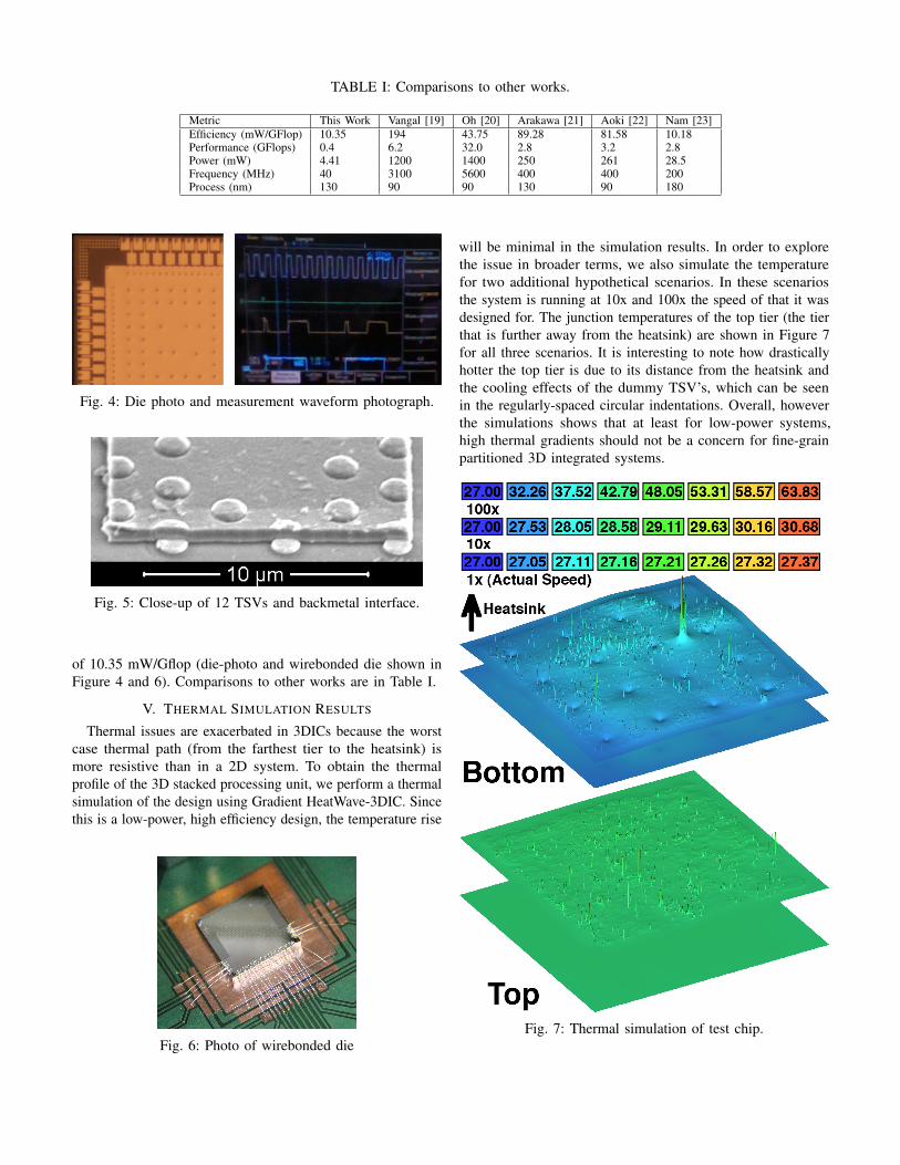
TABLE I: Comparisons to other works.
Metric This Work Vangal [19] Oh [20] Arakawa [21] Aoki [22] Nam [23]Efficiency (mW/GFlop) 10.35 194 43.75 89.28 81.58 10.18Performance (GFlops) 0.4 6.2 32.0 2.8 3.2 2.8Power (mW) 4.41 1200 1400 250 261 28.5Frequency (MHz) 40 3100 5600 400 400 200Process (nm) 130 90 90 130 90 180
Fig. 4: Die photo and measurement waveform photograph.
Fig. 5: Close-up of 12 TSVs and backmetal interface.
of 10.35 mW/Gflop (die-photo and wirebonded die shown inFigure 4 and 6). Comparisons to other works are in Table I.
V. THERMAL SIMULATION RESULTS
Thermal issues are exacerbated in 3DICs because the worstcase thermal path (from the farthest tier to the heatsink) ismore resistive than in a 2D system. To obtain the thermalprofile of the 3D stacked processing unit, we perform a thermalsimulation of the design using Gradient HeatWave-3DIC. Sincethis is a low-power, high efficiency design, the temperature rise
Fig. 6: Photo of wirebonded die
will be minimal in the simulation results. In order to explorethe issue in broader terms, we also simulate the temperaturefor two additional hypothetical scenarios. In these scenariosthe system is running at 10x and 100x the speed of that it wasdesigned for. The junction temperatures of the top tier (the tierthat is further away from the heatsink) are shown in Figure 7for all three scenarios. It is interesting to note how drasticallyhotter the top tier is due to its distance from the heatsink andthe cooling effects of the dummy TSV’s, which can be seenin the regularly-spaced circular indentations. Overall, howeverthe simulations shows that at least for low-power systems,high thermal gradients should not be a concern for fine-grainpartitioned 3D integrated systems.
Fig. 7: Thermal simulation of test chip.

VI. CONCLUSION
In this papers we have demonstrated a technique for 3Dstandard cell placement that includes a novel approach tokeeping all clocked cells one one tier. We have shown how thistechnique was used to create the first fine-grain partitioned 3Dintegrated system in the literature with silicon measurements.A SAR DSP chip with a measured operating efficiency of10.35 mW/Gflop which compares favorably to similar worksas demonstrated in Table I and summarized in Table II .Additionally, in this paper we have shown how a low powersystems such as this the SAR DSP avoid the thermal pitfallstypically associated with high-performance 3D integratedsystems with stacked dies.
Although the benefits of system-level 3D integrated systemsuch as DRAM on logic are more easily attainable and moreimmediate, we believe that there is a bright future for fine-grainpartitioned 3D integrated systems especially for high efficiencyand low power systems like the SAR DSP processing unit thatwas presented. However, this future will depend on advancesin microbump and TSV manufacturing, feature size and cost.
TABLE II: 3D Integrated SAR DSP Processor Summary.
Technology 130nm CMOSWiring 2 x (1P5M) + BMTransistors 149,936Test Circuit Area 0.3104 mm2
Die Size 5 mm x 5mmPower Supply 1.5 VFrequency 40 MHzCore Power 3.521 mW
ACKNOWLEDGMENTS
We thank Matthew Craver and Neil Di Spigna for their helpwith the assembly of the printed circuit boards and the test setup,Adi Srinivasan at Gradient Design Automation for help with thethermal simulation, along with Gary Yeap at Synopsys for hisadvice and support. This work was supported by SemiconductorResearch Corporation along with the MARCO Musyc Centerand GSRC Center, by DARPA under contract FA8650-04-C-7127 and contract FA8650-04-C-7120.
REFERENCES
[1] T. Zhang, K. Wang, Y. Feng, X. Song, L. Duan, Y. Xie, X. Cheng, andY.-L. Lin, “A customized design of dram controller for on-chip 3d dramstacking,” in CICC, 2010 IEEE, sept. 2010, pp. 1 –4.
[2] D. H. Kim, R. Topaloglu, and S. K. Lim, “Block-level 3d ic designwith through-silicon-via planning,” in Design Automation Conference(ASP-DAC), 2012, 30 2012-feb. 2 2012, pp. 335 –340.
[3] L. Xiao, S. Sinha, J. Xu, and E. Young, “Fixed-outline thermal-aware3d floorplanning,” in Design Automation Conference (ASP-DAC), 201015th Asia and South Pacific, jan. 2010, pp. 561 –567.
[4] J. Cong, J. Wei, and Y. Zhang, “A thermal-driven floorplanning algorithmfor 3D ICs,” in IEEE/ACM International Conference on Computer AidedDesign, 2004. ICCAD-2004, 2004, pp. 306–313.
[5] Y. Xie, G. H. Loh, B. Black, and K. Bernstein, “Design space explorationfor 3d architectures,” J. Emerg. Technol. Comput. Syst., vol. 2, no. 2, pp.65–103, 2006.
[6] M. Healy, K. Athikulwongse, R. Goel, M. Hossain, D. Kim, Y.-J. Lee,D. Lewis, T.-W. Lin, C. Liu, M. Jung, B. Ouellette, M. Pathak, H. Sane,G. Shen, D. H. Woo, X. Zhao, G. Loh, H. Lee, and S. K. Lim, “Designand analysis of 3d-maps: A many-core 3d processor with stacked memory,”in Custom Integrated Circuits Conference (CICC), 2010 IEEE, sept. 2010,pp. 1 –4.
[7] D. H. Kim, K. Athikulwongse, M. Healy, M. Hossain, M. Jung,I. Khorosh, G. Kumar, Y.-J. Lee, D. Lewis, T.-W. Lin, C. Liu, S. Panth,M. Pathak, M. Ren, G. Shen, T. Song, D. H. Woo, X. Zhao, J. Kim,H. Choi, G. Loh, H.-H. Lee, and S. K. Lim, “3d-maps: 3d massivelyparallel processor with stacked memory,” in Solid-State Circuits Confer-ence Digest of Technical Papers (ISSCC), 2012 IEEE International, feb.2012, pp. 188 –190.
[8] C. Mineo, R. Jenkal, S. Melamed, and W. Davis, “Inter-die signaling inthree dimensional integrated circuits,” Sept. 2008, pp. 655–658.
[9] Y. Liu, Y. Ma, E. Kursun, G. Reinman, and J. Cong, “Fine grain 3dintegration for microarchitecture design through cube packing exploration,”in Computer Design, 2007. ICCD 2007. 25th International Conferenceon, oct. 2007, pp. 259 –266.
[10] Y. Ma, Y. Liu, E. Kursun, G. Reinman, and J. Cong, “Investigating theeffects of fine-grain three-dimensional integration on microarchitecturedesign,” J. Emerg. Technol. Comput. Syst., vol. 4, no. 4, pp. 17:1–17:30,Nov. 2008.
[11] R. Hentschke, G. Flach, F. Pinto, and R. Reis, “Quadratic placement for3d circuits using z-cell shifting, 3d iterative refinement and simulatedannealing,” in SBCCI ’06: Proceedings of the 19th annual symposiumon Integrated circuits and systems design. New York, NY, USA: ACM,2006, pp. 220–225.
[12] S. Das, A. Chandrakasan, and R. Reif, “Design tools for 3-d integratedcircuits,” in ASPDAC 2003 conference on Asia South Pacific designautomation. New York, NY, USA: ACM, 2003, pp. 53–56.
[13] B. Goplen and S. Sapatnekar, “Efficient thermal placement of standardcells in 3d ics using a force directed approach,” Computer Aided Design,2003. ICCAD-2003. International Conference on, pp. 86–89, Nov. 2003.
[14] J. Cong, G. Luo, J. Wei, and Y. Zhang, “Thermal-aware 3d ic placementvia transformation,” in Design Automation Conference, 2007. ASP-DAC’07. Asia and South Pacific, Jan. 2007, pp. 780–785.
[15] J. Cong and G. Luo, “A multilevel analytical placement for 3d ics,” inASP-DAC ’09: Proceedings of the 2009 Asia and South Pacific DesignAutomation Conference. Piscataway, NJ, USA: IEEE Press, Jan. 2009,pp. 361–366.
[16] Y. Deng and W. Maly, “2.5d system integration: a design driven systemimplementation schema,” in Design Automation Conference, 2004. ASP-DAC 2004. Asia and South Pacific, jan. 2004, pp. 450 – 455.
[17] T. Thorolfsson, N. Moezzi-Madani, and P. Franzon, “Reconfigurable five-layer three-dimensional integrated memory-on-logic synthetic apertureradar processor,” Computers Digital Techniques, IET, vol. 5, no. 3, pp.198 –204, may 2011.
[18] R. Patti, “Three-dimensional integrated circuits and the future of system-on-chip designs,” Proceedings of the IEEE, vol. 94, no. 6, pp. 1214–1224,June 2006.
[19] S. Vangal, Y. Hoskote, N. Borkar, and A. Alvandpour, “A 6.2-gflopsfloating-point multiply-accumulator with conditional normalization,”JSSC, vol. 41, no. 10, pp. 2314–2323, Oct. 2006.
[20] H.-J. Oh, S. Mueller, C. Jacobi, K. Tran, S. Cottier, B. Michael,H. Nishikawa, Y. Totsuka, T. Namatame, N. Yano, T. Machida, andS. Dhong, “A fully pipelined single-precision floating-point unit in thesynergistic processor element of a cell processor,” Solid-State Circuits,IEEE Journal of, vol. 41, no. 4, pp. 759–771, April 2006.
[21] F. Arakawa, T. Yoshinaga, T. Hayashi, Y. Kiyoshige, T. Okada, M. Nishi-bori, T. Hiraoka, M. Ozawa, T. Kodama, T. Irita, T. Kamei, M. Ishikawa,Y. Nitta, O. Nishii, and T. Hattori, “An embedded processor core forconsumer appliances with 2.8gflops and 36m polygons/s fpu,” in Solid-State Circuits Conference, 2004. Digest of Technical Papers. ISSCC.2004 IEEE International, Feb. 2004, pp. 334–531 Vol.1.
[22] H. Aoki, T. Kawahara, M. Yamaoka, C. Yoshimura, Y. Nagasaka,K. Takayama, N. Sukegawa, Y. Fukumura, M. Nakahata, H. Sawamoto,M. Odaka, T. Sakurai, and K. Kasai, “A powerful yet ecological parallelprocessing system using execution-based adaptive power-down controland compact quadruple-precision assist fpus,” in VLSI Circuits, 2008IEEE Symposium on, june 2008, pp. 186 –187.
[23] B.-G. Nam and H.-J. Yoo, “A 28.5mw 2.8gflops floating-point multifunc-tion unit for handheld 3d graphics processors,” in Solid-State CircuitsConference, 2007. ASSCC ’07. IEEE Asian, Nov. 2007, pp. 376–379.
Related Documents