A 1-V CMOS Power Amplifier for Bluetooth Applications by Ho Ka Wai A Thesis Submitted to The Hong Kong University of Science and Technology in Partial Fulfillment of the Requirements for the Degree of Master of Philosophy in Electrical and Electronic Engineering August 2002, Hong Kong

Welcome message from author
This document is posted to help you gain knowledge. Please leave a comment to let me know what you think about it! Share it to your friends and learn new things together.
Transcript

A 1-V CMOS Power Amplifier for Bluetooth Applications
by
Ho Ka Wai
A Thesis Submitted to The Hong Kong University of Science and Technology
in Partial Fulfillment of the Requirements for the Degree of Master of Philosophy
in Electrical and Electronic Engineering
August 2002, Hong Kong

Authorization
I hereby declare that I am the sole author of the thesis.
I authorize the Hong Kong University of Science and Technology to lend this thesis to other institutions or individuals for the purpose of scholarly research.
I further authorize the Hong Kong University of Science and Technology to reproduce the thesis by photocopying or by other means, in total or in part, at the request of other institutions or individuals for the purpose of scholarly research.
Ho Ka Wai
ii

iii
A 1-V CMOS Power Amplifier for Bluetooth Applications
by
Ho Ka Wai
This is to certify that I have examined the above MPhil thesis and have found that it is complete and satisfactory in all respects,
and that any and all revisions required by the thesis examination committee have been made.
Dr. Howard Cam LUONG Thesis Supervisor Dr. Ross Murch Thesis Examination Committee Member (Chairman) Dr. Philip K. T. Mok Thesis Examination Committee Member Prof. Philip Ching-Ho Chan Head of Department of Electrical and Electronic Engineering
Department of Electrical and Electronic Engineering The Hong Kong University of Science and Technology
August 2002

Acknowledge
Acknowledge
I would like to take this opportunity to express my greatest gratitude to many
individuals who have given me a lot of supports during my two-year master program.
First of all, I am indebted to my thesis supervisor, Dr. Howard Cam Luong, for his
insight, the valuable guidance throughout the entire research and his patience in
reminding me to complete the works on time.
I would also be grateful to Frederick Kwok for his efficient technical support in
measurement setups and PCB making. Allen Ng for his patience in teaching me
how to use the bondwire machine. S. F. Luk for his kindly help in CAD tools and
chips tape-out.
I would like to thank my friends, Ming, Vincent, Gary, Gerry, Lincoln, Sun, Martin,
Joseph, Kenneth and Alan in analog research lab. They have given me a lot of
valuable suggestions in circuit design and provide enjoyment outside of the
university.
I would like to thank Dr. Ross Murch and Dr. Philip K. T. Mok for being my thesis
A 1V CMOS Power Amplifier for Bluetooth Applications iv

Acknowledge
A 1V CMOS Power Amplifier for Bluetooth Applications v
exam committee.
I would like to thank Agnes Au who does not mind working with me on holidays and
supports me by all means.
Finally, I would like to special thank my family for their encouragement and moral
support.

Table Of Contents
Table Of Contents
Title Page i
Authorization Page ii
Signature Page iii
Acknowledgment iv
Table Of Contents vi
List Of Figures ix
List Of Tables xii
Abstract xiii
Chapter 1 Introduction 1
1.1 Motivation 1
1.2 Specifications 3
1.3 Thesis Outline 5
Chapter 2 Basics Of Power Amplifier 8 2.1 Introduction 8
2.2 Figure Of Merits 9
2.3 Classifications Of Power Amplifiers 12
2.3.1 Linear Power Amplifiers 12
A 1V CMOS Power Amplifier for Bluetooth Applications vi

Table Of Contents
2.3.1.1 Class A 13
2.3.1.2 Class B 15
2.3.1.3 Class AB 18
2.3.2 Non-Linear Power Amplifiers 19
2.3.2.1 Class C 19
2.3.2.2 Class E 21
2.3.2.3 Class F 23
2.4 Summary 24
Chapter 3 Design Of Power Amplifier 27 3.1 Introduction 27
3.2 Design Of Power Amplifier 28
3.2.1 Differential Topology 28
3.2.2 Class-E Power Amplifier 29
3.2.3 Output Matching Network 31
3.2.4 Design Of Output Stage 33
3.2.5 Common-Gate Class-E Power Amplifier 35
3.2.6 Driver Stage Using Positive Feedback 39
3.2.7 Proposed Architecture 39
3.2.8 Pre-simulation Results 43
3.2.9 Inductor Realization 45
Chapter 4 Bondwire Modeling 48
4.1 Introduction 48
4.2 Inductor Model 49
4.3 Analytical Solution Of Bondwire Inductance 50
A 1V CMOS Power Amplifier for Bluetooth Applications vii
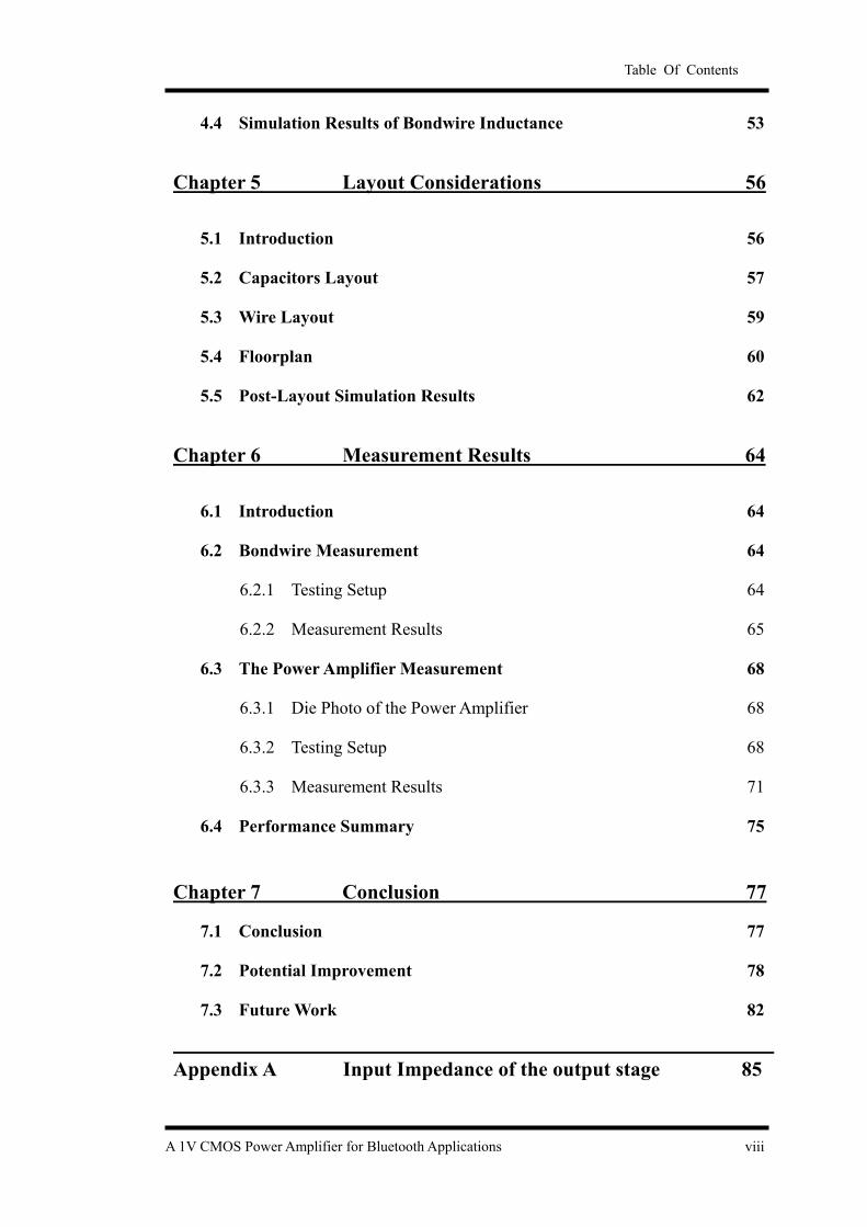
Table Of Contents
A 1V CMOS Power Amplifier for Bluetooth Applications viii
4.4 Simulation Results of Bondwire Inductance 53
Chapter 5 Layout Considerations 56 5.1 Introduction 56
5.2 Capacitors Layout 57
5.3 Wire Layout 59
5.4 Floorplan 60
5.5 Post-Layout Simulation Results 62
Chapter 6 Measurement Results 64 6.1 Introduction 64
6.2 Bondwire Measurement 64
6.2.1 Testing Setup 64
6.2.2 Measurement Results 65
6.3 The Power Amplifier Measurement 68
6.3.1 Die Photo of the Power Amplifier 68
6.3.2 Testing Setup 68
6.3.3 Measurement Results 71
6.4 Performance Summary 75
Chapter 7 Conclusion 77
7.1 Conclusion 77
7.2 Potential Improvement 78
7.3 Future Work 82
Appendix A Input Impedance of the output stage 85

List of Figures
List Of Figures
Figure 1.1 Output spectrum mask for class 1 Bluetooth 4
Figure 2.1 Definitions of IP3 and P1dB 10
Figure 2.2 Two-tone test of a power amplifier 10
Figure 2.3 Definition of ACPR 11
Figure 2.4 Typical configuration of a class-A power amplifier 13
Figure 2.5 Voltage and current waveforms of an ideal class-A power amplifier 14
Figure 2.6 Voltage and current waveforms of an ideal class-B power amplifier 16
Figure 2.7 Complementary class-B power amplifier 16
Figure 2.8 A transformer coupled class-B power amplifier 17
Figure 2.9 Voltage and current waveforms of an ideal class-AB power amplifier 18
Figure 2.10 Voltage and current waveforms of an ideal class-C power amplifier 20
Figure 2.11 A typical configuration of a class-E power amplifier 22
Figure 2.12 Voltage and current waveforms of an ideal class-E power amplifier 22
Figure 2.13 A simple configuration of a class-F power amplifier 23
Figure 2.14 Voltage and current waveforms of an ideal class-F power amplifier 24
Figure 3.1 Configuration of a class E power amplifier 29
Figure 3.2 Complete schematic of a class E power amplifier 32
Figure 3.3a A switch using common-source configuration 36
Figure 3.3b A switch using common-gate configuration 36
Figure 3.4 Schematic of the published common-gate class-E power amplifier 37
Figure 3.5 Schematic of the proposed common-gate class-E power amplifier 37
A 1V CMOS Power Amplifier for Bluetooth Applications ix

List of Figures
Figure 3.6 Voltage and current waveforms of a common-gate class E power
amplifier 38
Figure 3.7 Schematic of the proposed power amplifier 40
Figure 3.8 Equivalent schematic of the interstage-matching network 42
Figure 3.9 Transient response of the proposed power amplifier 44
Figure 3.10 PAE versus inductor Q 45
Figure 4.1 Lumped-element model for a bondwire inductor 49
Figure 4.2 Theoretical total inductance against the length of the wire 51
Figure 4.3 Simulated Inductance and quality factor against the length of the
bondwire 53
Figure 5.1 Polysilicon-polysilicon capacitor with parasitics 58
Figure 5.2 Capacitors inside the proposed power amplifier 59
Figure 5.3 Floorplan of the overall circuit 60
Figure 5.4 Circuit layout of the proposed power amplifier 61
Figure 5.5 Post-simulation on the transient response of the proposed power
amplifier 62
Figure 6.1 Testing setup for bondwire inductance 65
Figure 6.2 Simulated and measured S-parameter of open-pad testing setup 65
Figure 6.3 Simulated and measured S-parameter of bondwire measurement 66
Figure 6.4 A 1.2nH bondwire model 67
Figure 6.5 Photograph of the chip 68
Figure 6.6 Testing setup for the proposed power amplifier 69
Figure 6.7 Experimental prototype of the power amplifier 71
Figure 6.8 Output power and PAE versus supply voltage 72
A 1V CMOS Power Amplifier for Bluetooth Applications x

List of Figures
A 1V CMOS Power Amplifier for Bluetooth Applications xi
Figure 6.9 Output power and PAE versus frequency with 1V and 1.2V supply
voltage 73
Figure 6.10a The measured ACPR under 1V supply voltage 74
Figure 6.10b The measured ACPR under 1.2V supply voltage 74
Figure 7.1 Input power and supply voltage against the ratio of the input
device size to the size of the positive feedback device 81
Figure A1 Schematic of the output stage 85

List Of Tables
List Of Tables
Table 1.1 Transmit spectrum mask 4
Table 2.1 Performance summaries of different classes of power amplifiers 25
Table 3.1 Summary of the values of the passive components 43
Table 3.2 Summary of the transistors sizing 43
Table 3.3 Performance of the power amplifier 44
Table 5.1 Modified parameters for post-layout simulation 62
Table 5.2 Performance of the power amplifier 63
Table 6.1 Parameters for different inductors 67
Table 6.2 Summary of performance of the power amplifiers 75
Table 7.1 Summary of the simulation on the ratio of the size of the input
device to the positive feedback device
80
A 1V CMOS Power Amplifier for Bluetooth Applications xii

A 1-V CMOS Power Amplifier for Bluetooth Applications
by Ho Ka Wai
Department of Electrical and Electronic Engineering The Hong Kong University of Science and Technology
ABSTRACT
With recent advance in CMOS processes, many essential building blocks for wireless
transceivers, such as low-noise amplifier (LNA), mixer, frequency synthesizer,
channel selection filter and digital-to-analog converter, have been demonstrated
using CMOS technology. However, not much work has been done or reported a
CMOS power amplifier, in particular at low supply voltage. As supply voltage is
reduced to 1V, the performance of the power amplifier, such as the output power and
the efficiency are degraded.
In this thesis, the design considerations of a RF CMOS power amplifier under low
supply voltage are detailed. A two-stage power amplifier operated at 2.4GHz and
1-V supply has been designed and fabricated for Bluetooth applications in a standard
0.35µm CMOS technology. A common-gate Class E output stage, which operates
under low supply voltage without degrading the efficiency, is proposed. A
pre-amplifier with positive feedback configuration is employed to drive the
common-gate output stage. To achieve high efficiency and high output power,
xiii

xiv
bondwires are used as inductors for the power amplifier because of their high quality
factor.
Measurement results show that the amplifier delivers 18dBm output power with 33%
power-added efficiency (PAE) under a 1V supply voltage. With a 1.2V supply, the
amplifier delivers 20dBm output power with 35 % PAE and can be integrated for
class 1 Bluetooth application. The measured output spectrum falls within the
Bluetooth spectrum mask when a modulated signal is input to the power amplifier.
The adjacent-channel power rejection (ACPR) at 550kHz offset is –21.4 dBc under
1V and –23.5 dBc with 1.2V supply voltage.

Chapter 1: Introduction
CHAPTER 1
INTRODUCTION
1.1 Motivation
Wireless communications have shown remarkable growth in the last decade. For
example, more and more people have their own mobile phones. Some of them have
already owned several mobile phones in the past few years and are eager to buy new
phones with better performance. Manufacturers have to develop smaller mobile
phones with longer lifetimes and lower cost so as to keep competitive. Therefore,
experts in wireless communications put significant efforts to further improve the
performance and reduce the cost of the mobile phone.
Nowadays, the dominant technologies used for the radio frequency (RF) front-end
circuits of a mobile phone are Gallium Arsenide (GaAs), BiCMOS and silicon
bipolar. These technologies offer higher breakdown voltage, lower substrate loss
and higher quality of monolithic inductors and capacitors compared with CMOS
A 1V CMOS Power Amplifier for Bluetooth Applications 1

Chapter 1: Introduction
technology. However, they are much more expensive. CMOS technology is
exclusively used on the digital signal-processing unit. The realization of the RF
front-end circuits using CMOS technology can provide single-chip solution which
greatly reduces the cost. Moreover, the advance in CMOS process has made it
more possible to realize CMOS RF circuits with performance comparable to that
using GaAs, BiCMOS and silicon bipolar. Most of the essential building blocks of
a receiver, such as low noise amplifier (LNA), mixer, frequency synthesizer and
intermediate frequency (IF) filter, have been realized by CMOS processes [1][2].
Recently, short distance wireless communications, such as wireless local area
network (WLAN) and Bluetooth, have drawn the attention of researchers due to the
rapidly growth in personal communication systems. CMOS RF front-end circuits
are capable to meet the specifications so that the whole system can be integrated into
one chipset [3].
Although CMOS technology provides single chip solution, it also suffers from a poor
quality factor of monolithic passive components, low breakdown voltage of the
transistors and large process variation. Also, the scaling of the CMOS technology
forces the supply voltage to a lower level which results in degradation of the
performance of the transceiver.
A 1V CMOS Power Amplifier for Bluetooth Applications 2

Chapter 1: Introduction
Among all the building blocks of a transceiver, the power amplifier contributes the
most in terms of power consumption of the whole transceiver. The efficiency of the
power amplifier becomes one of the crucial parameters to be optimized for power
saving. However, the efficiency of the power amplifier is degraded by reducing
supply voltage.
This dissertation will focus on the design considerations and implementation of a
CMOS power amplifier for Bluetooth applications under low supply voltage.
1.2 Specifications
In this section, the specification of Bluetooth will be described. Also, the
requirement of power amplifier for Bluetooth applications will be detailed.
As the last building block of the transmitter, a RF power amplifier has to amplify the
RF signal before a RF signal is transmitted at the antenna. Because there are losses
in the channel, the signal power should be large enough so that the signal is still
readable at the receiver. Therefore, the output power of the power amplifier defines
the transmission distance of a communication standard.
Bluetooth is a short distance wireless communication standard which operates from
2400MHz to 2483.5MHz Industrial Scientific Medicine (ISM) band. Based on the
A 1V CMOS Power Amplifier for Bluetooth Applications 3

Chapter 1: Introduction
signal transmission distance, the required transmitter power level for Class 1, Class 2
and Class 3 are 20dBm, 4dBm and 0dBm, respectively. The modulation scheme
employed is Gaussian Frequency Shift Keying (GFSK) which is a constant envelope
modulation scheme [4]. Table 1.1 shows the requirement of the transmitted power
at certain frequency offset.
Table 1.1 Transmit spectrum mask
Frequency Offset Transmit Power
± 550 kHz -20 dBc |M-N| = 2 -20 dBm |M-N| ≥ 3 -20 dBm
According to table 1.1, the output spectrum of the power amplifier for Class-1
Bluetooth should be under the profile as shown below.
0
-10
-20
-30
-40
-50
-60
-70
-80
Relative Pow
er / dBc
0 500 1000 1500 2000 2500 3000 3500 Frequency Offset / kHz
Figure 1.1 Output spectrum mask for class 1 Bluetooth
A 1V CMOS Power Amplifier for Bluetooth Applications 4

Chapter 1: Introduction
Since the specification on linearity of the power amplifier is quite relaxed, non-linear
power amplifiers can be used to achieve high efficiency. The trade off between
linearity and efficiency will be detailed in chapter 2.
With the advance in process, the supply voltage is scaled down. The new market
trend is to build a single supply system with low operating voltage. Our research
group, the Analog Research Group, have demonstrated the use of 1-V supply voltage
in many essential building blocks such as low noise amplifier (LNA), mixer and
voltage-controlled oscillator (VCO) [5]. Therefore, the power amplifier will be
designed under 1-V supply voltage in order to fully integrate the whole transceiver.
The output power is targeted at 20dBm for Class 1 Bluetooth application.
1.3 Thesis Outline
In this thesis, there are 7 chapters. Some of the basics of power amplifier will be
detailed in chapter 2 to provide background information for the readers. Chapter 3
will discuss the design considerations of the power amplifier used for Bluetooth
applications. The inductor is one of the essential components in power amplifier
circuit. The modeling of the bondwire inductor will be described in chapter 4. In
chapter 5, both circuit and printed circuit board (PCB) layout considerations will be
presented. The measurement results of bondwire and the power amplifier will be
A 1V CMOS Power Amplifier for Bluetooth Applications 5

Chapter 1: Introduction
shown in chapter 6. The thesis ends with a conclusion in chapter 7 and talks about
the potential improvement of the circuit and the future work.
A 1V CMOS Power Amplifier for Bluetooth Applications 6

Chapter 1: Introduction
A 1V CMOS Power Amplifier for Bluetooth Applications 7
Reference [1] A. Rofougaran, G. Chang, J. J. Rael, J. Y. C. Chang, M. Rofougaran, P. J. Chang,
M. Djafari, M. K. Ku, E. W. Roth, A. A. Abidi, H. Samueli, “A Single-Chip 900-MHz Spread-Spectrum Wireless Transceiver in 1-µm CMOS Part II: Receiver Design,” IEEE J. Solid-State Circuits, pp. 535-547, April 1998.
[2] D. K. Shaeffer, A. R. Shahani, S. S. Mohan, H. Samavati, H. R. Rategh, M. del Mar Hershenson, X. Min, C. P. Yue, D. J. Eddleman, T. H. Lee, “A 115mW, 0.5µm CMOS GPS Receiver with Wide Dynamic-Range Active Filters,” IEEE J. Solid-State Circuits, pp. 2219-2231, Dec. 1998.
[3] H. Komurasaki, T. Heima, T. Miwa, K. Yamamoto, H. Wakada, L. Yasui, M. Ono, T. Sano, H. Sato, T. Miki, and N. Kato, “A 1.8-V operation RFCMOS transceiver for bluetooth,” Digest of VLSI Circuits Conference, pp 230-233, 2002.
[4] Bluetooth Specification v1.0b. [5] Chan A., Ng K., Wong J. and Luong H. C. "A 1-V 2.4-GHz RF Receiver
Front-End for Bluetooth Applications," IEEE International Symposium on Circuits and Systems 2001, pp. 454-457, Sydney, Australia, May 2001.

Chapter 2: Basics of Power Amplifier
CHAPTER 2
BASICS OF POWER AMPLIFIER
2.1 Introduction
Wherever there are wireless communications, there are transmitters. When there
are transmitters, there must be RF power amplifiers. People rate the performance of
an RF power amplifier in terms of the power gain, the efficiency and the linearity.
Also, the basic underlying principles of operations of different power amplifier
modes should be thoroughly understood before an improved circuit topology can be
designed. Therefore, understanding the language used in the world of power
amplifiers and the basic operating principle of different modes of power amplifier is
required.
In this chapter, the merits and the terminologies used to characterize a power
amplifier will be reviewed. Also, different classes of power amplifier and their
corresponding features will be described.
A 1V CMOS Power Amplifier for Bluetooth Applications 8

Chapter 2: Basics of Power Amplifier
2.2 Figure Of Merits
Whenever an RF power amplifier is discussed, people are interested in its power gain,
power-added efficiency (PAE), the drain efficiency (DE) and the linearity.
The power gain of a power amplifier is defined as follows:
inPoutP
portinput at the avaliablePower load the todeliveredPower Gain Power == (2.1)
The RF power amplifier consumes most of the power inside a transceiver. To
preserve the battery lifetime, the power amplifier should be effective in converting
DC power to RF power. PAE and DE are the parameters to characterize the
effectiveness of power conversion. They are defined as:
DCPoutP
DE = (2.2)
DCPinPoutP
PAE−
= (2.3)
where Pout is the output power at the desired frequency, PDC is the DC supply power
and Pin is the input power at the frequency of interest. PAE includes information on
the driving power for a power amplifier, so PAE is commonly used instead of DE.
It is observed that the PAE is approximately equal to the DE if the power gain is
A 1V CMOS Power Amplifier for Bluetooth Applications 9

Chapter 2: Basics of Power Amplifier
large enough. It also means that the power amplifier is more efficient.
Traditionally, linearity is measured with third order intermodulation intercept (IP3)
and 1dB compression point (P1dB). Figure 2.1 shows the graphic representations of
IP3 and P1dB.
Third harmonic
Fundamental frequency
1dB
Output Power / dBm
Input Power / dBm
OIP3
P1dB IIP3
Figure 2.1 Definitions of IP3 and P1dB
Those parameters can be obtained using a two-tone test [1] as pictured in Fig. 2.2.
Power
Amplifier
IM5
IM3
ω ∆ω ω
Figure 2.2 Two-tone test of a power amplifier
A 1V CMOS Power Amplifier for Bluetooth Applications 10

Chapter 2: Basics of Power Amplifier
By applying two single-tone signals with equal amplitude but with slightly different
frequencies circuit, the intermodulation products of the power amplifier are then
measured at the output.
However, IP3 and P1dB are not accurate enough and can only provide a rough
measure of linearity of a power amplifier. This is because most power amplifiers
operate near the 1dB compression point in order to achieve the highest efficiency,
and the nonlinear effects of higher order distortion should be taken into account.
Therefore, the adjacent-channel power rejection (ACPR) is used to assess the
linearity of a power amplifier instead of IP3 and P1dB. Figure 2.3 shows the
definition of ACPR.
Power
ω Adjacent Channel
Signal Channel
ACPR
Figure 2.3 Definition of ACPR
When a modulated signal is applied to the power amplifier, the output of the power
amplifier consists of the amplified signal channel and the adjacent channel signal
A 1V CMOS Power Amplifier for Bluetooth Applications 11

Chapter 2: Basics of Power Amplifier
resulted from intermodulation. Since the input used in testing the ACPR is a
modulated signal, higher order distortions are also included. Therefore, it is more
accurate to measure the linearity of a power amplifier using ACPR instead of a
two-tone test.
2.3 Classification Of Power Amplifiers
Digital modulation offers superior performance, such as noise insensitiveness and
integration of low cost CMOS process over analog modulation, and is widely used in
wireless systems. To facilitate discussion on the tradeoff between power efficiency
and spectral efficiency in digital modulation, literature classifies power amplifiers as
either linear power amplifiers or nonlinear power amplifiers [2].
2.3.1 Linear Power Amplifiers
When a linear power amplifier is used to amplify a signal, there is linear relationship
between the input signal and the output signal. This is important for the
non-constant envelope modulation scheme because the signal information, which is
embedded in the envelope, will be lost if the power amplifier is not linear enough.
Among all classes of power amplifiers, only class-A, class-AB and class-B can be
viewed as a linear power amplifier.
A 1V CMOS Power Amplifier for Bluetooth Applications 12

Chapter 2: Basics of Power Amplifier
2.3.1.1 Class A
A class-A power amplifier is the simplest power amplifier. It can be viewed as a
small-signal amplifier except the signal level is a substantial fraction of the bias level.
A typical circuit topology is shown in Fig. 2.4.
RFC
Vout
Vin
Vdd
Rload
Cblocking
Figure 2.4 Typical configuration of a class-A power amplifier
It consists of an RF choke, a DC blocking capacitor, a parallel LC tank and a
transistor. An RF choke (RFC) is used to feed DC power to the drain and provide a
constant current to the transistor. Also, the use of inductive load doubles the voltage swing at the drain of the transistor which lowers the supply voltage by a
factor of two [3]. The DC blocking capacitor prevents current flow to the output
loading in order to eliminate DC power consumption. Due to the non-linearity of
the transistor, the parallel LC tank filters the out-of-band emission so that only a
A 1V CMOS Power Amplifier for Bluetooth Applications 13

Chapter 2: Basics of Power Amplifier
single tone sine wave is observed across the output loading.
The NMOS transistor shown in Fig. 2.4 is operated in the saturation region or
pinch-off region for the whole input cycle. The transistor is biased to Vdd so that it
operates in the saturation region for the entire period. Since both the
transconductance (gm) and the output resistance (Rout) of the transistor remain the
same throughout the entire input cycle, the gain, gmRout, is approximately the same
throughout the period and the linearity is the best among the other classes of power
amplifier. Figure 2.5 shows the waveforms of a class-A power amplifier.
Vin Id Vds
Vdd
t t
Irf IDC
Vdd
t
Figure 2.5 Voltage and current waveforms of an ideal class-A power amplifier
However, due to the 100% duty cycle or 360° conduction angle, the transistor always
draws current during the period and the voltage across the transistor is always larger
than zero. In other words, the transistor dissipates power constantly throughout the
cycle. High linearity is achieved with the price of poor efficiency in a class-A
A 1V CMOS Power Amplifier for Bluetooth Applications 14

Chapter 2: Basics of Power Amplifier
power amplifier.
The efficiency can be derived with the fact that the transistor is biased at Vdd and the
amplitude of the output voltage swing is as large as Vdd. Also, the DC supply
current, IDC is the same as the RF current, Irf. Therefore, the DE of a class-A power
amplifier is:
21
ddVDCIddVrfI
21
DCPrfP
DE ===
The inherent DE of a class-A power amplifier is limited to 50%. Any non-ideal
effects, such as losses associated with the parasitics will further reduce the efficiency.
Therefore, the class-A power amplifier is chosen only when the requirement of
linearity is stringent.
2.3.1.2 Class B
It is noticed that the efficiency can be improved if the transistor does not conduct
current for the entire cycle, but only draws current at a certain period of time. For
example, if the transistor conducts half of the cycle, it is categorized as class-B
power amplifier. Because the transistor has a 180° conduction angle, the transistor
is biased at the threshold voltage and the transistor is in cut off region during half
period of time, as shown in Fig. 2.6.
A 1V CMOS Power Amplifier for Bluetooth Applications 15
Chapter 2: Basics of Power Amplifier
Vin Id Vds
Vth
2
T T
Vdd
t
t
t
Figure 2.6 Voltage and current waveforms of an ideal class-B power amplifier
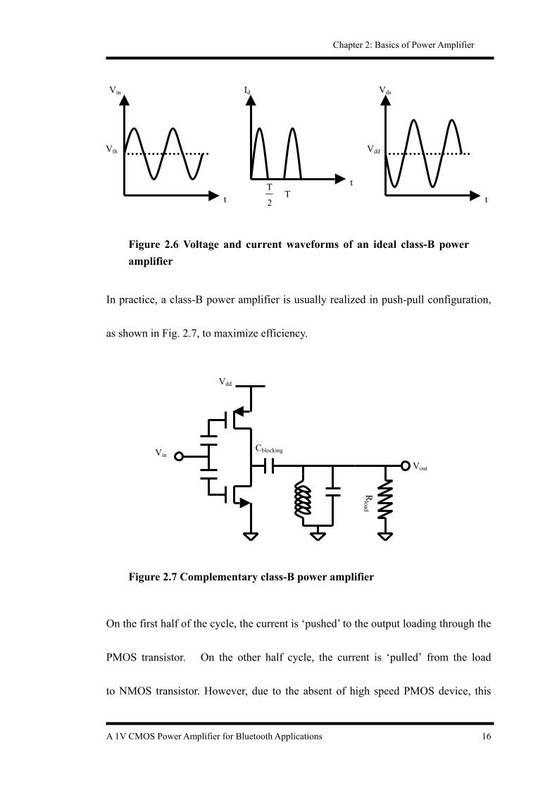
In practice, a class-B power amplifier is usually realized in push-pull configuration,
as shown in Fig. 2.7, to maximize efficiency.
Vout
Vdd
Rload
Cblocking
Vin
Figure 2.7 Complementary class-B power amplifier
On the first half of the cycle, the current is ‘pushed’ to the output loading through the
PMOS transistor. On the other half cycle, the current is ‘pulled’ from the load
to NMOS transistor. However, due to the absent of high speed PMOS device, this
A 1V CMOS Power Amplifier for Bluetooth Applications 16

Chapter 2: Basics of Power Amplifier
configuration is seldom used for RF applications.
As shown in Fig. 2.8, a transformer-coupled class-B power amplifier utilizes two
NMOS transistors.
T1
Vin-
Vout Vin+
Vdd
Rload
Figure 2.8 A transformer coupled class-B power amplifier
Since two NMOS transistors are used, it is more suitable for high-speed applications.
The transformer is used to combine the differential-ended drain current into a
single-ended current.
With a 50% duty cycle, the DE can achieve 78% [3]. However, the linearity is
inevitably degraded due to the switching between the cut-off region and the pinch-off
region of the transistors. In practice, a class-B power amplifier is difficult to
implement because the two transistors may have different threshold voltages and
they may be ON or OFF at the same time.
A 1V CMOS Power Amplifier for Bluetooth Applications 17

Chapter 2: Basics of Power Amplifier
2.3.1.3 Class AB
When the transistors are ON at the same time for some instant, the amplifier is
defined as a class-AB power amplifier. The corresponding waveforms are shown in
Fig. 2.9.
Vin Id Vds
Vth Vdd
t t
t
Figure 2.9 Voltage and current waveforms of an ideal class-AB power amplifier
As its name implies, all parameters associated with a class-AB power amplifier lie
between class-A and class-B. For example, the efficiency is between 50% and 78%.
The performance of linearity is somewhere between class-A and class-B. Since the
duty cycle of the transistors is ranged from 100% to 50%, the transistors are biased
above the threshold voltage.
The circuit topologies of a class-AB power amplifier can be either a simple transistor
configuration as class-A or a push-pull configuration as class-B. Class-AB power
amplifiers are widely used in a system with a non-constant envelope modulation
A 1V CMOS Power Amplifier for Bluetooth Applications 18

Chapter 2: Basics of Power Amplifier
scheme [4] since it can provide better linearity with acceptable efficiency.
2.3.2 Non-Linear Power Amplifiers
When a system employs constant envelope modulation scheme, the linearity of a
power amplifier is not critical. A non-linear power amplifier can be used so as to
obtain higher efficiency. Class-C, class-E and class-F are examples of non-linear
power amplifiers with high efficiency.
2.3.2.1 Class C
The efficiency of a power amplifier is increased from 50% for a class-A power
amplifier to 78% for a class-B power amplifier with the condition angle decreased
from 360° to 180°. It is observed that efficiency greater than 78% can be achieved
if the condition angle is further reduced to a level smaller than 180°. The resultant
power amplifier is categorized as class-C. In fact, the circuit topologies can be the
same for class-A, class-AB, class-B and class-C. The transistor in a class-A,
class-AB, class-B and class-C power amplifiers is operated as a current source. The
major difference associated with these four types of power amplifier is the biasing
condition. With the reduction in condition angle, the efficiency is traded-off with
the linearity from class-A to class-C. The price of achieving high efficiency is the
poor linearity performance. Moreover, although the efficiency can approach 100%
A 1V CMOS Power Amplifier for Bluetooth Applications 19

Chapter 2: Basics of Power Amplifier
with conduction angle trends to zero, the output power will be zero since there is no
drain current at all. Figure 2.10 shows the current and voltage waveforms of a
class-C power amplifier.
Vin Id Vds
Vth
2ϕ
Vdd
t t
t
Figure 2.10 Voltage and current waveforms of an ideal class-C power amplifier
From [5], the DE can be expressed in terms of ϕ where 2ϕ is the conduction angle
(in radian) for the class-C power amplifier:
−
=
2φcos
2φ
2φsin4
sinφ-φDE (2.4)
Equation 2.4 can also be applied to class-A with 2ϕ = 2π, class B with 2ϕ = π and
class-AB with π < 2ϕ < 2π.
When the conduction angle is reduced, the input driving power has to be increased in
order to maintain the device in the pinch-off regions which is essential to retain the
output power level. Among all of the conventional power amplifiers, the
A 1V CMOS Power Amplifier for Bluetooth Applications 20

Chapter 2: Basics of Power Amplifier
input-driving requirement of a class-C power amplifier is the largest. Therefore, a
class-C power amplifier is only suitable for a system with constant envelope
modulation scheme and low output power. For a system with high output power
and a constant envelope modulation scheme, switch mode power amplifier is used
which have both high output power and superior efficiency.
2.3.2.2 Class E
The class-E power amplifier was first invented by Sokal in 1975 [6]. Several
criteria have to be fulfilled for a power amplifier to be categorized as class-E. First
of all, voltage across the switch remains low when the switch turns off. When the
switch turns on, voltage across the switch should be zero. Finally, the first
derivative of the drain voltage with respect to time is zero, 0dtdsdV
= , when the
switch turns on. The first two conditions suggest that the power consumption by
the switch is zero. The last condition, 0dtdsdV
= , ensures that the voltage-current
product is minimized even if the switch has a finite switch on time. Figure 2.11
shows a typical configuration of a class-E power amplifier. L1 acts as either an RF
choke or a finite DC-feed inductance [7]. C2 and L2 are designed to be a series LC
resonator plus an excess inductance Lx at the frequency of interest. C1 and Lx are
designed so that the conditions for a class-E power amplifier operation are met.
A 1V CMOS Power Amplifier for Bluetooth Applications 21

Chapter 2: Basics of Power Amplifier
C1
Lx
L2
Vout
Vin
Vdd
Rload
C2
L1
Figure 2.11 A typical configuration of a class-E power amplifier
Figure 2.12 shows the waveforms of a class-E power amplifier.
Vds
Id
Vin OFF ON OFF ON OFF
t
t
t
Figure 2.12 Voltage and current waveforms of an ideal class-E power amplifier
It was observed that there is no overlapping between the voltage and the current
waveforms. Class-E power amplifiers achieve 100% efficiency theoretically in the
expense of poor linearity performance. However, the peak drain voltage is
approximately 3.6Vdd which increases the stress on the device especially for low
A 1V CMOS Power Amplifier for Bluetooth Applications 22

Chapter 2: Basics of Power Amplifier
breakdown CMOS process.
2.3.2.3 Class F
The idea of a class-F power amplifier is to exploit the harmonic contents so that the
drain voltage and current waveforms are shaped to achieve higher efficiency. A
sharper edge of the drain voltage will lower the loss of the switch. Therefore, a
square wave is desired at the drain. A parallel LC tank tuned to the third harmonic
is included to obtain the third harmonic component and add to the fundamental
component to approximate a square wave at the drain of the transistor. The circuit
configuration of a class-F power amplifier is shown in Fig. 2.13.
C1
L2
Vout
Vin
Vdd
Rload
Cblocking
RFC
C2
L1
Figure 2.13 A simple configuration of a class-F power amplifier
L1 and C1 are tuned to resonate at the fundamental frequency while L2 and C2 are
tuned to present non-zero load impedance at the third harmonic frequency to make
A 1V CMOS Power Amplifier for Bluetooth Applications 23

Chapter 2: Basics of Power Amplifier
up the second terms in the Fourier series expansion of a square wave. Figure 2.13
shows only the simplest class-F power amplifier with one LC tank tuned to the third
harmonic. Additional LC tanks can be added to resonate at other odd harmonic
frequencies to obtain a better square wave. The voltage and the current waveforms
shown in Fig. 2.14 will be observed.
Vds
Id
Vin OFF ON OFF ON OFF
t
t
t
Figure 2.14 Voltage and current waveforms of an ideal class-F power amplifier
A class-F power amplifier can achieve 100% efficiency ideally. However, the
disadvantage, in addition to the highly non-linear performance, is the complicated
circuit topology for scaling of 3rd harmonic.
2.4 Summary
This chapter provides background for the designer to choose a suitable power
amplifier. Efficiency and linearity are the major considerations when a class of
A 1V CMOS Power Amplifier for Bluetooth Applications 24
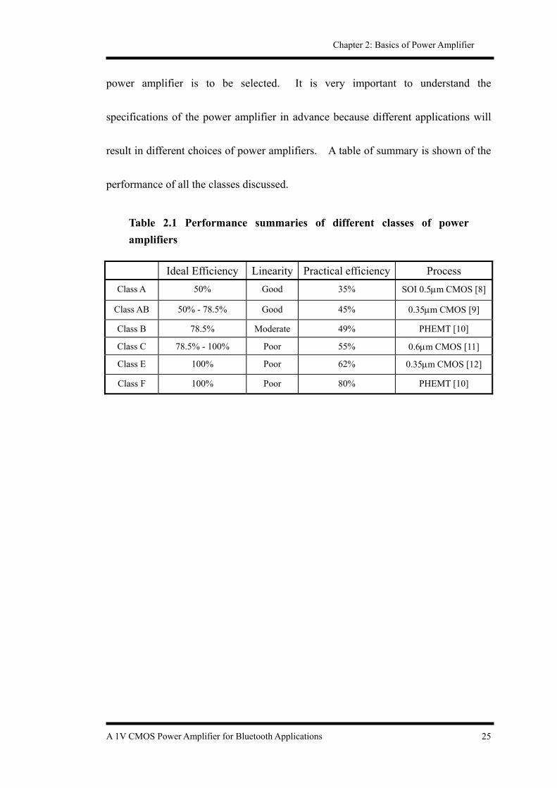
Chapter 2: Basics of Power Amplifier
power amplifier is to be selected. It is very important to understand the
specifications of the power amplifier in advance because different applications will
result in different choices of power amplifiers. A table of summary is shown of the
performance of all the classes discussed.
Table 2.1 Performance summaries of different classes of power amplifiers
Ideal Efficiency Linearity Practical efficiency Process Class A 50% Good 35% SOI 0.5µm CMOS [8]
Class AB 50% - 78.5% Good 45% 0.35µm CMOS [9]
Class B 78.5% Moderate 49% PHEMT [10]
Class C 78.5% - 100% Poor 55% 0.6µm CMOS [11]
Class E 100% Poor 62% 0.35µm CMOS [12]
Class F 100% Poor 80% PHEMT [10]
A 1V CMOS Power Amplifier for Bluetooth Applications 25

Chapter 2: Basics of Power Amplifier
A 1V CMOS Power Amplifier for Bluetooth Applications 26
Reference [1] R. Razavi, “RF Microelectronics”, 1998. [2] Steve C. Cripps, “RF Power Amplifiers for Wireless Communications”, 1999. [3] Thomas. H. Lee, “The Design of CMOS Radio-Frequency Integrated Circuits”,
1998. [4] J. T. Hwang, H. S. Lee, “1W 0.8µm BiCMOS adaptive Q-current controlled
class-AB power amplifier for portable sound equipments,” IEEE International Solid-State Circuits Conference, pp. 382-485, vol. 1, 2002.
[5] H. L. Kraus, C. W. Bostian, and F. H. Raab, “Solid State Radio Engineering”, 1980.
[6] N. Sokal and A. Sokal, “Class E – A New Class of High-Efficiency, Tuned Single-Ended Switching Power Amplifier”. IEEE J. Solid-State Circuits, vol. Sc-10, no. 3, pp. 168-176, June 1975.
[7] R. E. Zulinski and J. W. Steadman, “Class-E power amplifiers and frequency multipliers finite dc feed inductance”. IEEE Transitions on Circuits and Systems, vol. CAS-34, no. 9, pp. 1074-1087, September 1987.
[8] S. Lam, W. H. Ki, M. Chan, “Characteristics of RF power amplifiers by 0.5µm SOS CMOS process,” IEEE International SOI Conference, pp. 141-142, 2001.
[9] C. Fallesen, P. Asbeck, “A 1 W 0.35µm CMOS power amplifier for GSM-1800 with 45% PAE,” IEEE International Solid-State Circuits Conference, pp. 158-159, 2001.
[10] P. M. White, “Effect of input harmonic terminations on high efficiency class-B and class-F operation of PHEMT devices,” IEEE MTT-S Digest, vol. 3, pp. 1611-1614, 1998.
[11] R. Gupta, B. M. Ballweber, and D. J. Allstot, “Design and Optimization of CMOS RF Power Amplifiers”. IEEE J. Solid-State Circuits, vol. 36, no. 2, pp 166-175, Feb. 2001.
[12] K. Mertens, M. Steyaert, and B. Nauwelaers, “A 700-MHz 1-W Fully Differential CMOS Class-E Power Amplifier”. IEEE J. Solid-State Circuits, vol. 37, pp. 137-141, February 2002.
[13] T. C. Kuo, B. Lusignan, “A 1.5 W class-F RF power amplifier in 0.2µm CMOS technology,” IEEE International Solid-State Circuits Conference, pp. 154-155, 2001.

Chapter 3: Design of Power Amplifier
CHAPTER 3
DESIGN OF POWER AMPLIFIER
3.1 Introduction
Recall that the research goal is to design a CMOS power amplifier for Bluetooth
applications. Therefore, the corresponding specifications should be studied before
the design of the power amplifier.
As stated in chapter 1, the output power of the power amplifier is set to be 20dBm
for class-1 Bluetooth application under 1V supply voltage. Since the modulation
scheme employed by Bluetooth is GFSK, which is a constant envelope modulation
scheme, a non-linear power amplifier can be used to achieve high efficiency.
Among all classes of non-linear power amplifiers, the class-E power amplifier is the
most attractive candidate in terms of circuit simplicity and high efficiency
performance.
In this chapter, the circuit technique used for the power amplifier to work under low
A 1V CMOS Power Amplifier for Bluetooth Applications 27

Chapter 3: Design of Power Amplifier
supply voltage will be detailed in this chapter. Also, the design considerations of a
class-E power amplifier will be discussed. Both the calculated and the simulated
results will be presented. Finally, the characteristics of one of the crucial
components, the inductors, will be investigated.
3.2 Design of Power Amplifier
3.2.1 Differential Topology
Differential configuration will be adopted because of its numerous advantages.
First of all, the common-mode noise is minimized which reduces the disturbance of
substrate coupling to other circuits. Since the current is discharged to the ground
twice per cycle, interference to the desired signal is reduced.
A large output voltage swing is needed for a power amplifier so as to provide
moderate output power. However, the breakdown voltage of the devices in CMOS
process is too low to withstand a large voltage swing. With the process scaling, the
situation is even worse. Fortunately, the most pronounced advantage of differential
configuration, gain boosting, relaxes the stringent requirement on device breakdown
voltage. The same circuit topology with differential configuration gives double
output power compared with the single-ended configuration. Also, the size of the
A 1V CMOS Power Amplifier for Bluetooth Applications 28

Chapter 3: Design of Power Amplifier
transistor can be smaller because the current flow through the transistor is reduced
for the same supply voltage and the same output power.
3.2.2 Class-E Power Amplifier
The circuit topology of a class-E power amplifier is reprinted in Fig. 3.1.
C1
Lx
L2
Vout
Vin
Vdd
Rload
C2
L1
Figure 3.1 Configuration of a class E power amplifier
The component values can be calculated using the following equations [1]:
( )
+
−=
42outP2
422ddV
xLπω
ππ (3.1)
2ddV
outP1C
πω= (3.2)
outP
2ddV
0.577loadR = (3.3)
A 1V CMOS Power Amplifier for Bluetooth Applications 29

Chapter 3: Design of Power Amplifier
These equations can be derived by the fact that the switch is either turned on or off.
Therefore, two state equations can be obtained. For a power amplifier to be
categorized as class-E, several criteria, as stated in chapter two, have to be fulfilled.
These criteria are the boundary conditions to be applied and the state equations can
be solved.
It should be noted that the above equations are only valid for class-E power
amplifiers and Rload is not necessary the same for all classes of power amplifier [2].
Rload is usually called optimum load (Ropt) and is defined as a loading presented to the
power amplifier for a desired output power with the highest efficiency. The
optimum load is designed according to the specification on output power and the
supply voltage.
In the above analysis, L1 is assumed to be an RFC. The rule of thumbs for an
inductor to be an RFC is that the reactance of L1 is larger than ten times the reactance
of C1:
1C10X1LX > (3.4)
In fact, L1 acts as either a RF choke (RFC) or a finite DC-feed inductance.
However, it is advantageous to choose L1 as a finite DC-feed inductor because the
serial resistance of the inductor is reduced with a smaller inductance value which
A 1V CMOS Power Amplifier for Bluetooth Applications 30

Chapter 3: Design of Power Amplifier
provides higher efficiency than an RFC with the same output power and the same
supply voltage [3]. The operating frequency can be pushed higher with a finite
DC-feed inductor since the parasitic capacitors associated with the transistors are
resonated out by the inductor. In practice, the capacitor used to fulfill the class-E
operation, C1, can be implemented by the parasitic capacitance of the transistor.
Therefore, L1 can be calculated by the resonant equation of a LC tank.
−
==
1CpC2ω
1
C2ω
11L (3.5)
In the above equation, C is the total capacitance at the drain of the transistors, Cp,
minus the required parasitic capacitor, C1, in fulfilling the operating condition of a
class-E power amplifier.
3.2.3 Output Matching Network
The output power will be low if the power amplifier is directly connected to the
antenna, which has a 50Ω loading. For example, if Ropt = 50Ω and Vdd is 1V, then
11.54mWoptR
2ddV
0.577outP ==
As a result, the optimum load is typically about several ohms and can be obtained
with the supply voltage (Vdd) and the output power (Pout) fixed according to the
A 1V CMOS Power Amplifier for Bluetooth Applications 31

Chapter 3: Design of Power Amplifier
specification of a wireless standard.
In order to match the 50Ω loading, an up-conversion matching network is
implemented to transform the optimum load to a 50Ω load. L-matching network is
chosen because of its circuit simplicity. Also, the excess inductance (Lx) in a
class-E power amplifier can be combined with the inductor used in the matching
network if a low-pass L matching network is used. Therefore, the schematic of a
class-E power amplifier is modified as Fig. 3.2.
Low pass L Matching Network
Lm
Cm
Lx L2 Vout
Vin
Vdd
Ropt
C2 L
1
C1
Rload =50Ω
Figure 3.2 Complete schematic of a class E power amplifier
The values of Lm and Cm can be calculated using the following equations [4]:
ωoptRLRoptR
mL
−
= (3.6)
A 1V CMOS Power Amplifier for Bluetooth Applications 32

Chapter 3: Design of Power Amplifier
ωLR
optRoptRLR
mC
−
= (3.7)
3.2.4 Design Of Output Stage
Since the power amplifier is designed for class-1 Bluetooth application, the output
power is 20dBm, 100mW. The use of differential topology is to relax the output
power from 100mW to 50mW. The target output power is designed to be 60mW to
provide margin for some losses due to parasitics and the supply voltage of the power
amplifier is set to 1V. Therefore, the optimum load can be calculated using
equation 3.1.
( ) 9.6Ω0.57760m
142π
8
outP
2ddV
optR ==
+=
Also, the values of parameters, Lx and C1 can be calculated using equation 3.2 and
3.3 to meet the requirements of a class-E power amplifier.
( )0.735nH
42outP2
422ddV
xL =
+
−=
πω
ππ
1.27pF2ddV
outP1C ==
πω
With Ropt = 9.6Ω, the parameters of a L-matching network can be calculated using
A 1V CMOS Power Amplifier for Bluetooth Applications 33

Chapter 3: Design of Power Amplifier
equation 3.6 and 3.7.
1.31nHω
optR50optRmL =
−
=
2.72pFω50
optRoptR50
mC =
−
=
The parasitic capacitance associated with the transistor should be known before the
calculation of L1. As a result, the size of the transistor should be designed first in
order to find out the value of L1. However, the empirical equation to calculate the
transistor sizing is absent due to the apriori designability of the class E power
amplifier, the size of the transistor can only be estimated by the their maximum
allowable current flow.
Because the output power is set to 60mW and the supply voltage is 1V, the average
current flow through the transistor is about 60mA. Since the switch will conduct
current for only half of the period, the peak current should be at least 120mA. With
Vgs = Vds =1V, Vth =0.6V and µCox = 140µA/V2, the size of the transistor can be
calculated by the current equation:
2tVgsV
LW
2oxC
dI
−=
µ (3.8)
A 1V CMOS Power Amplifier for Bluetooth Applications 34

Chapter 3: Design of Power Amplifier
Because TSMC 0.35-µm CMOS will be used, the W/L of the transistor is found to be
approximately equal to 4500µ/0.4µ, which gives 4.2pF parasitic capacitors.
Therefore, L1 can be calculated by equation 3.5:
1.6nH
1CpC2ω
1
C2ω
11L =
−
==
3.2.5 Common-Gate Class E Power Amplifier
In the above analysis, all the components are assumed to be ideal. However, it is
not the case in practice. For example, the passive components, inductor and
capacitor, consist of parasitic serial resistances. Also, the switch has finite
on-resistance and finite transition times. As a result, the efficiency of a class-E
power amplifier is much degraded from theoretical 100% to the highest achievable
PAE of 63% in CMOS process [5]. Those non-ideal effects push RF circuit
designers to develop new circuit techniques to support low voltage design.
In a class-E power amplifier, the transistor acts as a switch instead of a current source.
The switch can be implemented by either common-source or common-gate
configuration. Usually, the switch is implemented using a common-source
configuration. For a common-source switch, the input signal is applied at the gate
of the transistor. The voltage across the transistor, Vds is fixed by the supply
A 1V CMOS Power Amplifier for Bluetooth Applications 35

Chapter 3: Design of Power Amplifier
voltage.
VO
+
VIN
_
(b)
Vdd
(a)
VO
+
VIN
_
Figure 3.3 A switch using (a) common-source (b) common-gate configuration
When the supply voltage is scaled down, the voltage dropped across the
on-resistance of the transistor is compatible to the supply voltage. The effective
supply voltage will decrease the power capability and hence degrade the efficiency.
onRVddVeffectiveV −= (3.9)
The situation is even worse if an RFC is used instead of a finite DC feed inductor.
Therefore, a finite DC feed inductor is preferred because the voltage drop across the
inductor is minimized and the effect on the effective supply voltage is neglected.
[6] proposed a common-gate class-E power amplifier to relax the device stress. The
corresponding schematic is shown in Fig. 3.4. The common-gate class-E power
amplifier is connected in cascode with a large transistor to avoid the loading effect to
the input stage. However, the cascode transistor unfortunately reduces the voltage
A 1V CMOS Power Amplifier for Bluetooth Applications 36

Chapter 3: Design of Power Amplifier
headroom across the switch.
Figure 3.4 Schematic of the published common-gate class-E power amplifier
To overcome the voltage drop across the switch, a common-gate switch without
connecting in cascode is proposed and the schematic of the proposed common-gate
class-E power amplifier is shown in Fig. 3.5.
VIN
Cm
Lm
50Ω
Cb
Lb
Vgg
Ropt
Vdd
Lx
C1
L1
0.5nH
50Ω 37pF 14pF
Input Stage
Vgg
Vdd
20pF
3.7nH
Figure 3.5 Schematic of the proposed common-gate class-E power amplifier
A 1V CMOS Power Amplifier for Bluetooth Applications 37

Chapter 3: Design of Power Amplifier
For a common-gate switch, the input signal is directly applied to the source. By
proper biasing, the effective supply voltage can be increased from Vdd – VRon (in the
common-source case) to Vdd –VRon + Vsignal where Vsignal is the amplitude of the input
signal. Figure 3.6 shows the corresponding current and voltage waveforms of the
proposed common-gate class E power amplifier.
Vds
Id
Vin OFF ON OFF ON OFF
t
t
t
Figure 3.6 Voltage and current waveforms of a common-gate class E power amplifier
The idea utilizes the fact that the voltage at the source is in phase with the voltage at
the drain. If the source is biased at ground and the gate is tied to Vdd, the switch is
turned on when the voltage of the source is negative. Since the input signal is
applied to the source, the amplitude of the signal increases the voltage across the
switch. As a result, the supply voltage is raised effectively. The effect of VRon can
be compensated by the amplitude of the applied signal in the common-gate
A 1V CMOS Power Amplifier for Bluetooth Applications 38

Chapter 3: Design of Power Amplifier
configuration, and the supply voltage can be lower with compatible efficiency. The
problem of low impedance of the input of the common-gate switch without cascode
can be solved with the inclusion of a driver stage with positive feedback before the
class-E amplifier.
3.2.6 Drive Stage Using Positive Feedback
The pre-amplifier of the power amplifier is a very important element since the
efficiency and the output power can be very low if the driving signal to the output
stage is not optimum. Under low supply voltage, the pre-amplifier is very hard to
design mainly because the size of the output stage transistors needs to be in
millimeter range, which introduces a large capacitive loading.
Because differential configuration is employed, the problem can be solved by
utilizing a cross-coupled pair to form a positive feedback as the pre-amplifier.
Several publications demonstrated the use of the positive feedback in power
amplifiers [5][7]. Also, a pre-amplifier with positive feedback provides a large
swing to the input of the output stage which maintains high efficiency.
3.2.7 Proposed Architecture
The overall schematic of the proposed power amplifier is shown in Fig. 3.7.
A 1V CMOS Power Amplifier for Bluetooth Applications 39

Chapter 3: Design of Power Amplifier
M3 M5 M6 M4 C
b
M2
M7
M1
Vdd
VBIA2
VBIA1
OUT+
Lmx
Cm
m
IN+ IN- OUT-
Lmx
Cd
Cd
Ld
Ld
L1
L1 L
2
L2
Lb
Lb
Cb
Figure 3.7 Schematic of the proposed power amplifier
The design of the proposed power amplifier starts by specifying the required power
gain and the output power. First of all, the output power is assumed to be 120mW,
20.8dBm. The power gain of the output stage is set to 7dB. Therefore, the
required input power for the output stage is 13.8dBm. In other words, the output
power of the driver stage should be at least 13.8dBm. The input power to a power
amplifier utilizing positive feedback input stage is around 3dBm [5][7]. As a result,
the power gain of the driver stage is equal to 10.8dBm. It is always the case that the
power gain of the input stage is higher than the output stage because the input stage
is focused on high power gain while the output stage is targeted to achieve high
efficiency.
A 1V CMOS Power Amplifier for Bluetooth Applications 40

Chapter 3: Design of Power Amplifier
Since the DC biasing points for the drain of the driver stage and the source of the
output stage are different, an interstage-matching network with a DC blocking
capacitor, Cd, is implemented to connect the driver stage and the output stage.
Another function of the interstage-matching network is to present an optimum load
to the driver stage while transfer the maximum power to the input of the output stage.
Since the driver stage using positive feedback works as a class-E power amplifier,
the values of the components of the driver stage can be calculated using the same
agreement as the output stage.
( ) Ω480.57712m
142π
8)preamp(oP
2ddV
)preamp(optR ==
+=
( )2nH
42)preamp(oP2
422ddV
)preamp(xL =
+πω
−ππ=
0.253pF2ddV
(preamp)oP)preamp(1C =
πω=
2.4nH
2CpC2ω
1
C2ω
12L =
−
==
The impedance looking from the source of the output stage to the 50Ω load is
calculated as shown below:
A 1V CMOS Power Amplifier for Bluetooth Applications 41

Chapter 3: Design of Power Amplifier
−−+−−++
−+
+=
1L1
1L
pC2
mxLj1
pC
1L21
mC
mxL
pC
mC
1L2
LR
1m
Cmx
L2ωL
R1
Ljmx
L1
L2
m1g
1Z
ωωωω
ωω
Since all the parameters have been designed, the impedance Z is found to be:
j13.1518.36Z +=
The biasing LC tank Lb and Cb is to bias the source of the output stage to ground and
can be separated into two parts: a LC tank resonates at the frequency of interest and a
matching network, Ly and Cd, for matching the impedance Z and Ropt(preamp).
Figure 3.8 shows the equivalent schematic of the interstage-matching network.
Z
Sources of the output stage Drains of the driver stage
Ld Cd Lbias
Cbias
Ly
Figure 3.8 Equivalent schematic of the interstage-matching network
Since the capacitor Cbias will be implemented by the parastics capacitance of Cd
which will be detailed in Chapter 5, Cbias is chosen to be one fifth of Cd and the
inductor Lbias can be calculated using the resonant equation:
A 1V CMOS Power Amplifier for Bluetooth Applications 42

Chapter 3: Design of Power Amplifier
biasC2ω
1biasL =
Table 3.1 summarizes the values of the passive components used in the power
amplifier.
Table 3.1 Summary of the values of the passive components
L1 L2 Lm Cm Lb Cb Ld Cd
1.6nH 2.4nH 2nH 1.36pF 1.9nH 0.55pF 2nH 4.2pF
Table 3.2 summarized the sizing of the transistors used in the proposed power
amplifier. The corresponding parasitic drain capacitances, Cp, are also shown and
the capacitances are used to calculate the finite DC feed inductors, L1 and L2.
Table 3.2 Summary of the transistors sizing
M1 M2 M3 M4 M5 M6 M7
W 4500µm 4500µm 600µm 600µm 1200µm 1200µm 12000µm
L 0.4µm 0.4µm 0.4µm 0.4µm 0.4µm 0.4µm 0.4µm
Cp 4.2pF 4.2pF 0.78pF 0.78pF 1.35pF 1.35pF 17pF
3.2.7 Pre-simulation Results
The proposed power amplifier is simulated using Hspice. Level 49 BSIM3 model
for TSMC 0.35-µm double-polysilicon 4-metal layer process is used throughout the
A 1V CMOS Power Amplifier for Bluetooth Applications 43

Chapter 3: Design of Power Amplifier
simulation. The performance of the proposed power amplifier is summarized in
Table 3.3.
Table 3.3 Performance of the proposed power amplifier
Frequency Supply Voltage Input Power Output Power Power Gain DE PAE
Calculated 2.4GHz 1V - 120mW 17.8dB 100% -
Simulated 2.4GHz 1V 3dBm 116.7mW 17.6dB 65.1% 63.8%
The DE is only 65.1% because the transistors have a finite transition time which
introduced overlapping of the voltage and the current waveforms. In addition to the
power dissipation due to the finite transition time, the on-resistor of the switch
degrades the efficiency.
Figure 3.9 shows the waveforms of the drain of the driver stage (Vdi), the drain of the
output stage (Vdo) and the source of the output stage (Vs).
Vs
Vdi Vdo Vout
Figure 3.9 Transient response of the proposed power amplifier
A 1V CMOS Power Amplifier for Bluetooth Applications 44

Chapter 3: Design of Power Amplifier
It can be seen that the voltage at the source of the output stage swings to a negative
value which increases the effective supply voltage.
3.2.8 Inductor Realization
In the pre-simulation, all the passive components are ideal. The parasitic serial
resistance of both the capacitor and the inductor are assumed to be zero. In practice,
the efficiency depends highly on the quality of the passive components especially the
inductors. The quality of an inductor can be justified by quality factor (Q):
RLQ ω
= (3.10)
To investigate the effect on the inductor Q, PAE of the proposed power amplifier is
plotted against Q in Fig. 3.10.
0
10
20
30
60
70
0 20 40 60 80 100 120Q
40
50PAE / %
Figure 3.10 PAE versus inductor Q
It is observed that the PAE drops rapidly when the Q is below 20. Therefore, the
A 1V CMOS Power Amplifier for Bluetooth Applications 45

Chapter 3: Design of Power Amplifier
inductor Q should be kept at a level higher than 20 for acceptable PAE.
CMOS monolithic inductors are well known for its low quality factor (Q) due to high
substrate loss and high parasitics. Monolithic inductors are widely used in RF
applications even when the Q of monolithic inductors ranges from 3 to 6 in the
CMOS process. Many building blocks, such as LNA and VCO, use monolithic
inductors with Q-compensation circuitry [8]. These methods of Q compensation of
on-chip inductors, however, are not feasible in power amplifiers because the power
consumed in compensating the inductor losses would significantly lower the
efficiency. Therefore, bondwire inductors are used to implement high-Q inductors
to obtain a higher PAE.
A 1V CMOS Power Amplifier for Bluetooth Applications 46

Chapter 3: Design of Power Amplifier
A 1V CMOS Power Amplifier for Bluetooth Applications 47
Reference [1] N. Sokal and A. Sokal, “Class E – A New Class of High-Efficiency, Tuned
Single-Ended Switching Power Amplifier”. IEEE J. Solid-State Circuits, vol. Sc-10, no. 3, pp. 168-176, June 1975.
[2] R. Gupta, B. M. Ballweber, and D. J. Allstot, “Design and Optimization of CMOS RF Power Amplifiers”. IEEE J. Solid-State Circuits, vol. 36, no. 2, pp 166-175, Feb. 2001.
[3] R. E. Zulinski and J. W. Steadman, “Class-E power amplifiers and frequency multipliers with finite dc feed inductance”. IEEE Transitions on Circuits and Systems, vol. CAS-34, no. 9, pp. 1074-1087, September 1987.
[4] D. M. Pozar, “Microwave Engineering”, 1993. [5] K. Mertens, M. Steyaert, and B. Nauwelaers, “A 700-MHz 1-W Fully
Differential CMOS Class-E Power Amplifier”. IEEE J. Solid-State Circuits, vol. 37, pp. 137-141, February 2002.
[6] C. Yoo and Q. Huang, “A common-gate switch 0.9-W class-E power amplifier with 41% PAE in 0.25µm CMOS”. IEEE J. Solid-State Circuits, vol. 36, No. 5, pp. 823-830, May 2001.
[7] K. C. Tsai and P. R. Gray, “1.9-GHz 1-W CMOS RF power amplifier for wireless communication”. IEEE J. Solid-State Circuits, vol. 34, pp. 962-970, July 1999.
[8] Y. W. Chung and Y. H. Shuo, “The Design of a 3-V 900-MHz CMOS Bandpass Amplifier”. IEEE J. of Solid-State Circuits, vol. 32, No. 2, Feb. 1997.

Chapter 4: Bondwire Modeling
CHAPTER 4
BONDWIRE MODELING
4.1 Introduction
In chapter 3, the design of the proposed power amplifier and the pre-simulation
results were presented. However, it is possible that measurement results cannot
match the simulation results if the modeling of the components used is not accurately
done. Although the model of the transistors (the level 49 BSIM3 model) is accurate
enough, the model of another essential component, inductor, is still inaccurate in RF
applications.
In the design of the power amplifier, all the inductors are realized using bondwire.
Because of the high quality factor offered by bondwire which reduces resistive power
losses, a higher PAE can be obtained. Although bondwire inductors provide a high
quality factor, predetermination of bondwire inductance is difficult. Since the
inductance is sensitive to bonding geometry, bondwires need to be modeled
A 1V CMOS Power Amplifier for Bluetooth Applications 48

Chapter 4: Bondwire Modeling
accurately before they can be used as inductors in a power amplifier.
In this chapter, the model used for bondwire inductor will be introduced and the
quantitative analysis of the inductance will be presented. The analytical solution
will provide a rough estimation of the relationship between the inductance and the
physical length of the bondwire which facilitates both the circuit layout and the PCB
layout. Finally, the simulation of the bondwire inductance and the quality factor
will be done using HP’s ADS.
4.2 Inductor Model
In order to have an accurate model, all the elements used in the inductor model have
to be well defined according to the electromagnetic theory and the physical structure.
Figure 4.1 shows a lumped element model for the bondwire inductor.
Ls Rs
Rp
Rp
Cp
Cp
Port 1 Port 2
Figure 4.1 Lumped-element model for a bondwire inductor
A 1V CMOS Power Amplifier for Bluetooth Applications 49

Chapter 4: Bondwire Modeling
Ls is the inductance of the bondwire, Rs models the serial resistor, Cp accounts for the
overlap capacitance between the inductor and the ground plate and Rp models the
substrate loss. This model will be used to do the empirical fit of the measurement
results in chapter 6.
4.3 Analytical Solution Of Bondwire Inductance
The inductance of a wire can be calculated by equation 4.1 [1]:
+
+−+
++
= δrµ
21
2
2ld1
2ld2
12
d2ll
d2lln
2πloµ
L (4.1)
=
ds4d
0.25tanhδ (4.2)
rµofµρ
sdπ
= (4.3)
where l is the length of the wire, d is the diameter of the wire, ρ is the resistivity of
the material of the wire, ds is the skin depth and µo, µr are the absolute permeability
and the relative permeability of the wire respectively.
The inductance of the wire will be decreased if the wire close to the ground plate.
The negative mutual inductance caused by the ground plate is give by [1]:
A 1V CMOS Power Amplifier for Bluetooth Applications 50

Chapter 4: Bondwire Modeling
+−+
++
=
21
2
l2h1
l2h2
12
2hl1
2hlln
2πloµ
M(2h) (4.4)
where h is the distance between the ground plate and the inductor. As a result, the
total inductance of the wire is reduced to ( )2hMLtotalL −= .
Since aluminum bondwire with 1.25-mil diameter will be used,
, , m8101.75ρ Ω−×= 1.00002rµ = 1Hm7104oµ −−×= π and .
Also,
m31.75d µ=
2mm2h = because the bondwire is typically 1mm above the ground plate.
The theoretical total inductance of the wire is plotted against the length of the wire in
Fig. 4.2.
L
M(2h)
Ltotal
Figure 4.2 Theoretical total inductance (Ltotal) against the length of the wire
A 1V CMOS Power Amplifier for Bluetooth Applications 51

Chapter 4: Bondwire Modeling
Several inductance values will be used in the proposed power amplifier. For
example, the RFC of the input stage and the output stage are 2.3nH and 1.6nH
respectively. Also, 2nH inductors are used in the output of the power amplifier and
the interstage matching. Their corresponding lengths can be found in Fig. 4.2.
The resistance of the bondwire can be estimated using the following equation
AlρRS = (4.5)
where l is the length of the wire, A is the effective area of the wire, ρ is the resistivity
of the material of the wire. Because of the skin effect [2], the effective area of the
wire is reduced from 2
2dπ
to
−
−
2s
2
2d2d
2dπ .
For example, the serial resistance, RS, of inductance with 2nH can be calculated by
equation 4.5 with l = 2.65mm, m8101.75ρ Ω−×= and m31.75d µ= :
0.357Ω
2µ718.231.75µ
231.75µπ
102.65101.75Alρ(2nH)R
22
38
S =
−
−
××==
−−
Therefore, the quality factor of the bondwire inductor with 2nH inductance is:
84.5R
LQS
==ω
A 1V CMOS Power Amplifier for Bluetooth Applications 52

Chapter 4: Bondwire Modeling
4.4 Simulation Results of Bondwire Inductance
The analytical equations, however, do not accurately provide information on the
quality factor of an inductor. Fortunately, commercial software, HP’s ADS,
contains a function to simulate the bondwire inductance and the quality factor as long
as the physical parameters are provided. For example, the length of the bondwire,
the height of the bondwire to the ground plate and conductivity of the material used.
Since aluminum bondwire with 1.25-mil diameter will be used, the same
parameters,ρ ,m8101.75 Ω−×= 1.00002rµ = , 1Hm7104oµ −−×= π , 2h = 2mm
and , are inputted. The relationships of the length with both the
inductance and the quality factor are shown in Fig. 4.3 with the frequency fixed to
2.4GHz.
m31.75µd =
Quality factor
Length of the bondwire / mm
Inductance/nH
Figure 4.3 Simulated Inductance (asterisk marked) and quality factor (circle marked) against the length of the bondwire
A 1V CMOS Power Amplifier for Bluetooth Applications 53

Chapter 4: Bondwire Modeling
The inductance and the quality factor are found by the Y-parameters [3]. It is
observed that the quality factor increases with the length of the bondwire. This is
because when the bondwire is longer, the eddy current induced by the ground plate
will decrease, which results in smaller losses. The quality factor remains constant
when the effect of the ground plate is neglected. From the simulation, the quality
factor is at least 30 and can be used in the power amplifier without severely
degrading the PAE.
A 1V CMOS Power Amplifier for Bluetooth Applications 54

Chapter 4: Bondwire Modeling
A 1V CMOS Power Amplifier for Bluetooth Applications 55
Reference [1] A. M. Niknejad, R. G. Meyer, “Design, Simulation and Applications of
Inductors and Transformers for Si RFICS”, 2000. [2] Pieter L. D. Abrie, “The Design of Impedance-matching Networks for
Radio-Frequecny and Microwave Amplifiers”, 1985. [3] R. L. Bunch, D. I. Sanderson, S. Raman, “Quality Factor and Inductance in
Differential IC Implementations,” IEEE Microwave Magazine, pp. 82-92, June 2002.

Chapter 5: Layout Considerations
CHAPTER 5
LAYOUT CONSIDERATIONS
5.1 Introduction
Due to the enormous current flow in a power amplifier compared to other building
blocks, a 100 mV reduction in the output voltage swings will result when there is
only 0.2Ω parasitic resistor. Therefore, the layouts of the power amplifier have to
be carefully designed so that the performance of the circuit will not be degraded.
In this chapter, some layouts of the components will be detailed. For example, the
layouts of the capacitor and the interconnection wire will be discussed. Because
bondwire will be used as the inductors, the floorplan and the layout of the overall
circuit as well as the PCB will be presented. Finally, the post-simulation results
will be given.
A 1V CMOS Power Amplifier for Bluetooth Applications 56
Chapter 5: Layout Considerations
5.2 Capacitors Layout
There are numerous approaches used when drawing the layout of capacitors,
metal-metal capacitors, polysilicon-polysilicon capacitors and substrate-well
capacitors. Among all the layout techniques, the capacitor using
polysilicon-polysilicon provides the highest capacitance density. However, some of
the process does not offer double polysilicon layers for capacitors realization.
Fortunately, the TSMC 0.35-µm process offers double polysilicon layers, so the
layout of the capacitors will be drawn using double polysilicon layers.
Two important issues have to be considered for the layout of the capacitors.
First of all, the serial resistance of the capacitors layout should be minimized
especially when the capacitor is in the signal path of the circuit. The resistivity of
polysilicon is larger compared with the resistivity of metal. The large resistivity of
polysilicon contributes the most to the serial resistance of the capacitor. Therefore,
the dimension of the polysilicon should be small enough to minimize the serial
resistance and large capacitance can be realized using fingers. Also, the
interconnection should use metal as the media instead of polysilicon.
Contacts are used to connect the polysilicon to the metal. Since a contact
contributes 6.9Ω resistance, many contacts have to be present to minimize the serial
A 1V CMOS Power Amplifier for Bluetooth Applications 57

Chapter 5: Layout Considerations
resistance. As a result, the layout of a polysilicon-polysilicon capacitor should be
similar to the one shown in Fig. 5.1.
Rc Rc Rc Rc Rc
Rc Rc Rc Rc Rc
Cp
Rp1 Rp1
Rc
Port 1 Port 1 Port 2
C
Rp2
Metal 1
Contact
Poly 2
Contact
Poly 1
Substrate
Figure 5.1 Polysilicon-polysilicon capacitor with parasitics
Secondly, the parasitic capacitance introduced by the capacitor itself should be taken
into account. A parasitic capacitor (Cp) is formed between the lower polysilicon
layer and the substrate. This parasitic capacitor is accompanied with the wanted
polysilicon-polysilicon capacitor (C) where C is about 5 times Cp. Therefore, the
ports should be assigned carefully depending on the circuit. For example, port 2
should be assigned to a node which is more sensitive to the parasitics while the
parasitic should have negligible effect for the node connected to port 1.
Figure 5.2 extracts the part of the schematic of the proposed power amplifier
containing the capacitors.
A 1V CMOS Power Amplifier for Bluetooth Applications 58

Chapter 5: Layout Considerations
Cb
Ld
Lb
Drains of the driver stage
Sources of the output stage
Cd
Lb
Cb
Ld Cd
Figure 5.2 Capacitors inside the proposed power amplifier
It is observed that the capacitor Cd can be implemented by the
polysilicon-polysilicon capacitor while the parasitic capacitor as discussed is utilized
as the capacitor Cb. Therefore, the area of the capacitors layout can be reduced and
the parasitic effect can be eliminated.
5.3 Wire Layout
Due to the finite current density of the metal layers, even the simplest component,
the interconnecting wire, has to be designed carefully so that the width is large
enough to allow a large current to flow without burning the wire.
By rule of thumb, a metal slab with thickness of 1-µm is capable of handling 1mA of
current. Since there are approximately 40mA of current flow in the driver stage and
100mA of current drawn from the output stage, the corresponding widths of the
A 1V CMOS Power Amplifier for Bluetooth Applications 59

Chapter 5: Layout Considerations
metal are 40µm and 100µm. Although metal 4, which is about 1.4 times thicker
than other metal layers, reduces the width to 29µm and 72µm, respectively, these
wide metals introduce an undesirably large parasitic capacitor with the substrate.
Therefore, two or three metal layers are connected in parallel so as to minimize the
parasitic capacitor. In order to eliminate the capacitor formed between the metals, a
large number of via are added to reduce the potential difference.
5.4 Floorplan
Figure 5.3 shows the block diagram of the overall layout.
Driver R
FC
Driver R
FC
Interstage Inductor
Source B
iasing
Source B
iasing
Output R
FC
Output R
FC
Output -
Output +
GND
VBIA
VBIA
Input +
Input -
Capacitor
Capacitor
Driver
Output Stage
Current Source
Interstage Inductor
Figure 5.3 Floorplan of the overall circuit
A 1V CMOS Power Amplifier for Bluetooth Applications 60

Chapter 5: Layout Considerations
Since all the inductors are realized by bondwires, the layouts of the pads as well as
the circuits are placed to facilities bonding of the bondwires.
Figure 5.4 shows the final layout of the proposed power amplifier. The area of the
chip is 0.9 x 0.8 mm2.
0.9 mm
0.8 mm
Figure 5.4 Circuit layout of the proposed power amplifier
A 1V CMOS Power Amplifier for Bluetooth Applications 61

Chapter 5: Layout Considerations
5.5 Post-Layout Simulation Results
Due to the parasitics introduced by the circuit layout, some of the values of the
inductors are reduced to optimize the performance of the overall circuit. The
modified inductances are shown in Table 5.1.
Table 5.1 Modified parameters for post-layout simulation
L1 L2 Lm Cm Lb Cb Ld Cd
0.9nH 2nH 1.8nH 1.5pF 1.2nH 0.8pF 1.8nH 4.5pF
Figure 5.5 shows the waveforms of the drain of the driver stage (Vdi), the drain of the
output stage (Vdo) and the source of the output stage (Vs).
Vout
Vdi
Vdo
Vs
Figure 5.5 Post-simulation on the transient response of the proposed power amplifier
A 1V CMOS Power Amplifier for Bluetooth Applications 62

Chapter 5: Layout Considerations
A 1V CMOS Power Amplifier for Bluetooth Applications 63
Apart from the changes made to the inductances, the quality factors of the inductors
are also included in the post simulation.
Both the calculated result and the pre-simulated result are reprinted for comparison.
The performance of the power amplifier is summarized in Table 5.2. The output
power is 19dBm with 35% PAE. The degradation of the performance is mainly due
to the inclusion of the quality factors of the inductors. All the inductors assume a
quality factor of 30.
Table 5.2 Performance of the power amplifier
Frequency Supply Voltage Input Power Output Power Power Gain DE PAE
Calculated 2.4GHz 1V - 120mW 17.8dB 100% -
Pre-sim 2.4GHz 1V 3dBm 116.7mW 17.6dB 65.1% 63.8%
Post-sim 2.4GHz 1V 3dBm 78mW 15.8dB 37% 35%

Chapter 6: Measurement Results
CHAPTER 6
MEASUREMENT RESULTS
6.1 Introduction
In this chapter, both the testing setups and the measurement results for the bondwire
and the power amplifier will be presented. The calibration for bondwire modeling
and the inductor model will be detailed. Moreover, the procedure for measuring the
power amplifier will be illustrated and the measurement results of the power
amplifier will be given out.
6.2 Bondwire Measurement
6.2.1 Testing Setup
Figure 6.1 shows the testing setup for bondwire measurement. The setup is targeted
on 1-port measurement of the bondwire inductance. It consists of a SMA connector,
a microstrip line with 50Ω characteristic impedance and a 1mm gap for bonding the
wire.
A 1V CMOS Power Amplifier for Bluetooth Applications 64

Chapter 6: Measurement Results
50Ω Microstrip line SMA connector
Via Bondwire
Network Analysis
Figure 6.1 Testing setup for bondwire inductance
6.2.2 Measurement Results
Before the bondwire inductance is measured, the effects on SMA connector and the
microstrip line should be calibrated out. Figure 6.2 shows the simulation result and
the measurement result of the SMA connector and the microstrip line.
S11
S22
S22
S11
Figure 6.2 Simulated (S11) and measured (S22) S-parameter of open-pad testing setup
A 1V CMOS Power Amplifier for Bluetooth Applications 65

Chapter 6: Measurement Results
The calibration setup of the SMA connector is the same as shown in Fig. 6.1 except
that the bondwire is removed. It is observed that the SMA model fit the
measurement results from 1GHz to 3GHz and the frequency range for Bluetooth
application, 2.4GHz to 2.48GHz, is covered.
A bondwire is bonded across the gap and the setup is then measured again. The
model described in chapter 4 is used to fit the measured result. Figure 6.3 shows
the simulated (S11) and the measured (S22) S-parameters.
S11
S22
S11
S22
Figure 6.3 Simulated (S11) and measured (S22) S-parameter of bondwire measurement
The simulation results of the overall model, including the SMA connector and the
bondwire inductor, also fit the measurement results from 1GHz to 3GHz. By
A 1V CMOS Power Amplifier for Bluetooth Applications 66

Chapter 6: Measurement Results
varying the loop of the bonding machine, the lengths of the bondwire are changed
accordingly. Several models are used to fit the measured results with the same
procedures described above. Figure 6.4 shows an example of the bondwire models
which gives 1.2nH with the quality factor equals 27 at 2.4GHz.
Ls = 1.2nH Rs = 0.68Ω
Rp = 6.71mΩ
Port 1
Cp = 53.5fF
Figure 6.4 A 1.2nH bondwire model
Several inductors with different inductances will be used for the proposed
power amplifier. Table 6.1 shows the parameters of the inductors used.
Table 6.1 Parameters for different inductors
Ls Rs Cp Rp Q Biasing Inductor 1.2nH 0.68Ω 53.5fF 6.71mΩ 27 Output RFC 0.97nH 0.54Ω 58.8fF 136mΩ 27 Input RFC Output Matching Interstage Matching
1.94nH
0.47Ω
87.3fF
35mΩ
62
A 1V CMOS Power Amplifier for Bluetooth Applications 67

Chapter 6: Measurement Results
6.3 The Power Amplifier Measurement
6.3.1 Die Photo of the Power Amplifier
Figure 6.5 shows the photograph of the power amplifier fabricated in a 0.35-µm
4M2P standard CMOS process with the threshold voltage of NMOS transistor equals
0.65V (VTN = 0.65V). The chip area, which including bonding pad, is 0.8 mm x 0.9
mm.
Capacitors
Preamp Stage
Output
Stage
Figure 6.5 Photograph of the chip
6.3.2 Testing Setup
A commercial power splitter, AMPS H-183-4, is used to provide a differential
input signal. A commercial power combiner (AMPS H-183-4) is used at the
output to convert the differential output to the single-ended output. There are
A 1V CMOS Power Amplifier for Bluetooth Applications 68

Chapter 6: Measurement Results
5.1dB loss associated with the coaxial cables and the splitter. The signal
generator used provide functions on generating a GFSK output signal for
Bluetooth, so the ACPR can be measured with the same testing setup by
changing the generated signal from single-tone sine wave to GFSK modulated
signal.
Figure 6.6 shows the testing setup for the proposed power amplifier.
Power Combiner
Bias-T
Device Under Test
Bias-T
Power Splitter
Signal Generator
Spectrum Analysis
Figure 6.6 Testing setup for the proposed power amplifier
The bare die is directly attached to the PCB ground plate. Due to the unavailable of
conductive epoxy, silver paint is used to fix the die to the PCB. All the inductors
are realized using 1.25-mil aluminum bondwire. Since the bondwire inductance is
highly dependent on the bonding geometry, the PCB is carefully designed to
A 1V CMOS Power Amplifier for Bluetooth Applications 69

Chapter 6: Measurement Results
facilitate wire bonding especially for the interstage inductors. The interstage
inductors are implemented by bonding the wire from the die to the PCB and then
bonded back from the PCB to the die. Also, since the inductors used in biasing the
common-gate switch is directly connected to the ground plate of the PCB, the
inductance can be very small.
As the input impedance is not 50Ω, an L-matching network is designed using
equations 3.6 and 3.7 to allow maximum power transfer from the signal generator to
the input of the power amplifier. The actual input power applied to the power
amplifier is measured at the input pad of the bare die using high impedance probe so
that the losses associated with the input matching network is calibrated out.
Another important issue is the calibration of the high impedance probe. As long as
the calibration of the high impedance is accuracy, the power measured provides
accuracy information on the input power at the input of the power amplifier. The
calibration of the high impedance probe is done by probing an open pad using a
high-speed probe, which have a 50Ω impedance and the power is measured by the
high impedance probe. Since the power is well defined for the high-speed probe,
the power loss associated with the high impedance probe can be calibrated out. The
degree of accuracy of the calibration will be dependent on how well the actual input
impedance of the power amplifier is matched to the impedance of the calibration set
A 1V CMOS Power Amplifier for Bluetooth Applications 70

Chapter 6: Measurement Results
up, which is the impedance of the open pad in parallel with the impedance of the
high-speed probe.
The experimental prototype is shown in Fig. 6.7.
Figure 6.7 Experimental prototype of the power amplifier
6.3.3 Measurement Results
Figure 6.8 shows the measured output power and the measured PAE against the
supply voltage.
It is observed that the dependence of the output power is approximately proportional
to Vdd2. The simulation results are also presented for comparison. The measured
output power shows agreement with the simulated output power. At 1V, the power
amplifier delivers 68mW with 33% PAE. When the supply voltage is increased to
A 1V CMOS Power Amplifier for Bluetooth Applications 71

Chapter 6: Measurement Results
1.2V, the PAE raised to 35% with 102mW output power.
Simulation: dotted line
Measurement: solid line
Supply Voltage (V)
0.22 0.2 0.18 0.16 0.14 0.12 0.1 0.08 0.06 0.04 0.02 0
60
55
50
45
40
35
30 1 1.1 1.2 1.3 1.4 1.5
Output Pow
er / W
PAE / %
Figure 6.8 Output power and PAE versus supply voltage
Both the simulated results and the measurement results shown that the PAE do not
have significant improvement when the supply voltage is increased. It is because
the voltage drop across turn-on resistor is neglected when the supply voltage is
increased. The effective supply voltage defined in equation 3.9 will approximately
equal to the supply voltage. Since the DC biasing currents of the transistors are
remaining unchanged when the supply voltage is increased, the total power
dissipation and the output power is larger at the same time which resulted in a
constant PAE.
Figure 6.9 shows the measured output power and the PAE versus the frequency range
of the Bluetooth specification with 1V and 1.2V supply voltage.
A 1V CMOS Power Amplifier for Bluetooth Applications 72

Chapter 6: Measurement Results
Output Pow
er (W)
PAE (%
)
Frequency (GHz)
Figure 6.9 Output power and PAE versus frequency with 1V (shown in solid line) and 1.2V supply voltage (shown in dotted line)
The power amplifier achieves 34.5% PAE and gives 77mW output power at 2.45GHz
under 1V supply. The PAE maintain at least 33% over the frequency range from
2.4GHz to 2.48GHz. At 1.2V supply voltage, the amplifier gives 20dBm output
power with at least 35% PAE which can be integrated for Class-1 Bluetooth
application.
In order to verify the operation with the bluetooth specification, a GFSK modulated
signal with BT equals 0.5 is applied to the power amplifier.
Figure 6.10 shows the measured ACPR under 1V and 1.2V supply voltage and the
measurements are made using a 100 kHz resolution bandwidth and a 30 kHz video
bandwidth.
A 1V CMOS Power Amplifier for Bluetooth Applications 73

Chapter 6: Measurement Results
(b)
(a)
Figure 6.10 The measured ACPR under (a) 1V and (b) 1.2V supply voltage
Both the measured output spectrums of the proposed power amplifier with 1V and
1.2V fall within the spectrum mask of the Bluetooth specifications. For 1V, the
ACPR at 550kHz frequency offset is –21.4-dBc while 23.5-dBc is measured for 1.2V
supply voltage.
A 1V CMOS Power Amplifier for Bluetooth Applications 74

Chapter 6: Measurement Results
6.4 Performance Summary
Table 6.2 summarizes the performance of the proposed power amplifier. The
existing literature of the power amplifier is also shown for comparison. This work
is the first power amplifier targeted on 1V supply voltage.
Table 6.2 Summary of performance of the power amplifiers
[1] [2] [3] This Work
Process 0.25µm CMOS 0.35µm CMOS 0.25µm CMOS 0.35µm CMOS
Supply Voltage 1.8V 2V 2.5V 1V 1.2V
Frequency 900MHz 1.9GHz 2.4GHz 2.4GHz 2.4GHz
PAE 41% 48% 48% 33% 35%
Output Power 0.9W 1W 0.23W 77W 120mW
ACPR @ ± 550 kHz - - - -21.4dBc -23.5dBc
A 1V CMOS Power Amplifier for Bluetooth Applications 75

Chapter 6: Measurement Results
A 1V CMOS Power Amplifier for Bluetooth Applications 76
Reference [1] C. Yoo and Q. Huang, “A common-gate switch 0.9-W class-E power amplifier
with 41% PAE in 0.25µm CMOS”. IEEE J. Solid-State Circuits, vol. 36, No. 5, pp. 823-830, May 2001.
[2] K. C. Tsai and P. R. Gray, “1.9-GHz 1-W CMOS RF power amplifier for wireless communication”. IEEE J. Solid-State Circuits, vol. 34, pp. 962-970, July 1999.
[3] Vathulya V. R., Sowlati T. and Leenaerts D. “Class 1 Bluetooth Power Amplifier with 24dBm Output Power and 48% PAE at 2.4GHz in 0.25µm CMOS”. European Solid State Circuits Conference, Villach, Austria, September 2001.

Chapter 7: Conclusion
CHAPTER 7
CONCLUSION
7.1 Conclusion
This thesis attempted to build a low voltage RF power amplifier prototype for
Bluetooth applications. Different classes of power amplifiers are reviewed and the
design considerations for power amplifiers were investigated.
The power amplifier was implemented in a differential configuration in order to
minimize the amount of substrate current injected at the signal frequency. A
two-stage power amplifier operated at 2.4GHz with 20.8dBm output power with 1V
supply voltage and 63.8% PAE is designed and simulated. The common-gate class
E output stage is implemented to compensate the effect on scaling of the supply by
proper biasing the common-gate switch. The pre-amplifier stage utilized the
positive feedback configuration to drive the low impedance common-gate switch.
One of the most essential components, an inductor, was realized using bonding wire
A 1V CMOS Power Amplifier for Bluetooth Applications 77

Chapter 7: Conclusion
because of its high quality factor compared with on-chip spiral inductor. The
modeling of the bondwire inductor is also done. The quality factor of the bondwire
is measured to be at least 26, which is high enough for power amplifier application.
The bare die was assembled on the PCB with all necessary DC supply and the
output-matching network of the power amplifier. The PCB was designed to
facilitate the wire bonding. The measurement results showed that the power
amplifier had achieved 34.5% PAE and gave 77mW output power at 2.45GHz under
1V supply. At 1.2V supply voltage, the amplifier gave 20dBm output power with
35% PAE which can be integrated for Class 1 Bluetooth application.
With the trend of decreasing supply voltage of the whole system, a power amplifier
with low operating voltage is desired for realizing a single chip, single supply
transceiver. The proposed power amplifier can be integrated with others building
blocks to provide a low cost fully CMOS transceiver in the future.
7.2 Potential Improvement
Although the proposed power amplifier can work at supply voltage as low as 1V, the
PAE of the power amplifier still have room to be improved. First of all, the margin
for the power losses of the power amplifier should be set larger in the design phase
so that the output power can be higher at 1V supply voltage. Therefore, the size of
A 1V CMOS Power Amplifier for Bluetooth Applications 78
Chapter 7: Conclusion
the output stage should be bigger to allow larger current to obtain higher output
power. However, there is limitation on increasing the transistor size. Since the
parasitics associated with the transistor will also increase when the size of the
transistor is larger, the finite DC feed inductance will be too small to be implemented
in practice and it is proved that the quality factor of the bondwire inductor will
decrease for smaller inductance. Moreover, when the finite DC feed inductance is
too small, the feed inductance does not allow constant input current and the voltage
swing at the drain of the output stage will decrease. As a result, both the output
power and efficiency will be degraded. Once the circuit is fabricated, the only way
to have larger output power is to increase the supply voltage which is not desired if a
single low supply voltage system is wanted.
Secondly, although bondwires offer quality factor as high as 62, the variation of
bondwire inductance is about 10% which will degrade the performance of the power
amplifier especially at high frequency operation. The precision of the bondwire
inductance is limited by the bonding machine. The situation will be improved if an
automatic bonding machine with the function of inductance estimation is available.
In fact, the most desired solution is to have a monolithic inductor with high quality
factor. However, 0.35µm CMOS process can only provide on chip spiral inductor
with highest quality factor of 4 and is not suitable for the power amplifier circuitry.
A 1V CMOS Power Amplifier for Bluetooth Applications 79

Chapter 7: Conclusion
Moreover, the ratio of the size of the input device to the size of the positive feedback
device can be designed to optimize the performance of the proposed power amplifier.
To investigate the relationship of the transistor size between the input device and the
positive feedback device, the ratio of the transistor size is varied and the details of
the simulation is summarized in Table 7.1.
Table 7.1 Summary of the simulation on the ratio of the size of the input device to the positive feedback device
Ratio WI LI WP LP gmI + gmP Output Power Total Drain Capacitance
0.4 50µm 0.4µm 125µm 0.4µm 189m A/V 0.118mW 1.71pF
0.5 600µm 0.4µm 1200µm 0.4µm 190m A/V 0.121mW 1.72pF
0.6 680µm 0.4µm 1130µm 0.4µm 190.6m A/V 0.120mW 1.72pF
In the simulation, the proposed power amplifier shown in Fig. 3.7 is simulated and
the ratio of the size of the input device to the positive feedback device is varied.
The output power, the total transconductance and the total drain capacitance of the
input stage are kept unchanged to compare the effect of the ratio of the transistor on
both the input power and the supply voltage. Since the total transconductance and
the total drain capacitance vary with supply voltage, Table 7.1 only shows the
condition at 1V supply voltage. The conditions under other supply voltage can be
easily found with the given parameters.
Fig. 7.1 shows the plot of the input power of the power amplifier and the supply
A 1V CMOS Power Amplifier for Bluetooth Applications 80

Chapter 7: Conclusion
voltage against the ratio of the transistor size between the input device and the
positive feedback device.
Figure 7.1 Input power and supply voltage against the ratio of the input device size to the size of the positive feedback device
Intuitively, the size of the input device should be smaller so that the previous stage of
the power amplifier, such as the up-conversion mixer, can drive the preamp stage of
the power amplifier. However, it is observed that the required input power for
locking the drain voltage of the input stage have to be larger when the ratio of the
input device size to the positive feedback device size is small. It is because the
current flow through the input device is not large enough to lock the drain voltage of
the input stage. Since the drain voltage of a class-E power amplifier can be as high
A 1V CMOS Power Amplifier for Bluetooth Applications 81

Chapter 7: Conclusion
as 3.56 x Vdd, the input power has to be larger when the supply voltage is increased.
As a result, an additional buffer stage has to be added which resulted in larger power
dissipation of the whole system. Therefore, the ratio of the size of the input device
to the positive feedback device should be chosen to be the same to minimize the
driving input power.
With the advance in CMOS process, 0.18µm CMOS process provide options such as
thick metal layer to design on chip spiral inductor with quality factor as high as 10.
Also, since the feature size of the device is decreased, the finite turn-on and turn-off
time becomes smaller and the power losses associated with the transistors is
decreased with the same operating frequency. The power amplifier can be fully
integrated with trade-off on the performance of the efficiency.
7.3 Future Work
CMOS power amplifier for WLAN application is another potential research topic.
However, there are several problems needed to be solved. First of all, the operating
frequency for WLAN application is 5GHz, the modeling of bondwire inductor in
5GHz is still absent. The method described in chapter 4 to model the bondwire
inductor is not applicable because the SMA model is only applied to frequency up to
3GHz. A novel methodology has to be developed to model the bondwire inductor if
A 1V CMOS Power Amplifier for Bluetooth Applications 82

Chapter 7: Conclusion
bondwire inductor has to be used. Another approach to realize an inductor is to use
on chip inductor. Although 0.18µm CMOS process should be used for frequency as
high as 5GHz, the quality factor of CMOS monolithic inductor is still limited to
around 10. Moreover, the linearity requirement is –20dBc at 11MHz frequency
offset with the signal bandwidth limited to 9MHz frequency offset for the
specification of 802.11a. Since the degree of non-linearity of the active device
increased with frequency, linear power amplifier has to be used or linearization
techniques such as pre-distortion [1], feed-forward [2] and feedback [3] have to be
applied to the non-linear power amplifier which resulted in degradation of efficiency
performance. Therefore, in order to design a power amplifier for WLAN
application with low supply voltage, the linearity has to be traded-off with the
efficiency unless some novel circuit technique is developed for high frequency
application.
A 1V CMOS Power Amplifier for Bluetooth Applications 83

Chapter 7: Conclusion
A 1V CMOS Power Amplifier for Bluetooth Applications 84
Reference
[1] A. Zhu, T. J. Brazil, “An adaptive Volterra predistorter for the linearization of RF high power amplifiers”. IEEE MTT-S International Microwave Symposium, vol. 1, pp. 461-464, 2002.
[2] Y. Y. Woo, Y. Yang, J. Yi, J. Nam, J. H. Cha, B. Kim, “Feedforward amplifier for WCDMA base stations with a new adaptive control method”. IEEE MTT-S International Microwave Symposium, vol. 2, pp. 769-772, 2002.
[3] J. S. Chang, H. G. Bah, S. L. Yong, T. T. Meng, “A novel low-power low-voltage Class D amplifier with feedback for improving THD, power efficiency and gain linearity”. IEEE International Symposium on Circuits and Systems, vol. 1, pp. 635-638, 2001.

Appendix A: Input Impedance of the Output Stage
APPENDIX A
INPUT IMPEDANCE OF THE OUTPUT STAGE
L1
Z2 Z1
Z3
Z
Cm
Lmx Vgg
Vdd C
1
RL
Figure A1 Schematic of the output stage
LRmCjLR
LRmC
XZω+
==1
1
112
211213
1
212
112
CLjZZLj
CZLZ
LRmCjmxLjmCmxLLRZ
LRmCjLRmxLjZ
mxLXZ
ω
ω
ω
ωω
ωω
+==
+
+
−
=
++=+=
A 1V CMOS Power Amplifier for Bluetooth Applications 85

Appendix A: Input Impedance of the Output Stage
A 1V CMOS Power Amplifier for Bluetooth Applications 86
( )( ) ( )
( ) ( )
( ) ( )[ ]1111211121112
1211
23
1
111
21
122113
111
211
22113
LCLmxLjCLmCmxLCmCLLR
mCmxLLRLjLmxLZ
Cj
mxLLjmCmxLLLR
mxLLmCmxLLRLjZ
CmxLLjmCmxLLLR
mxLLmCmxLLRLjZ
−−+
−
−++
−+
=
−
+++
+−
−
−
=
++
+−
−−=
ωωωω
ωωω
ωωω
ωωω
ωω
ωωω
+=
−−+−−++
−+
+=
1L1
1L
pC2
mxLj1
pC
1L21
mC
mxL
pC
mC
1L2
LR
1m
Cmx
L2ωL
R1
Ljmx
L1
L2
m1g
1Z
3m1g1Z
ωωωω
ωω
Z
Related Documents


![Operational Transconductance Amplifier (OTA) in 45nm CMOS · Amplifier (OTA) in 45nm CMOS YOUNGSEOK LEE ... Design of Analog CMOS Integrated Circuits. McGraw-Hill, 2002. [2] B. Ahuja,](https://static.cupdf.com/doc/110x72/5fbfc7035b7a87264a188ff5/operational-transconductance-amplifier-ota-in-45nm-cmos-amplifier-ota-in-45nm.jpg)


