ACCESS IC LAB Graduate Institute of Electronics Engineering, NTU 98-1 Under-Graduate Project Digital IC Design Flow Speaker: 銀子駒 Adviser: Prof. An-Yeu Wu Date: 2010/09/21

Welcome message from author
This document is posted to help you gain knowledge. Please leave a comment to let me know what you think about it! Share it to your friends and learn new things together.
Transcript

ACCESS IC LAB
Graduate Institute of Electronics Engineering, NTU
98-1 Under-Graduate Project
Digital IC Design Flow
Speaker: 銀子駒
Adviser: Prof. An-Yeu Wu
Date: 2010/09/21
ACCESS IC LAB Graduate Institute of Electronics Engineering, NTU
P. 2
Outline
Introduction to Integrated Circuit
IC Design Flow
Verilog HDL concept
Verilog Simulator
ACCESS IC LAB Graduate Institute of Electronics Engineering, NTU
P. 3
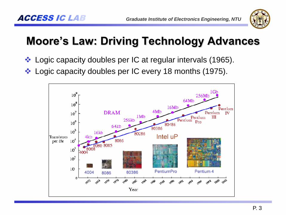
Moore’s Law: Driving Technology Advances
Logic capacity doubles per IC at regular intervals (1965).
Logic capacity doubles per IC every 18 months (1975).

ACCESS IC LAB Graduate Institute of Electronics Engineering, NTU
P. 4
Chips Sizes
Source: IBM and Dataquest
ACCESS IC LAB Graduate Institute of Electronics Engineering, NTU
P. 5
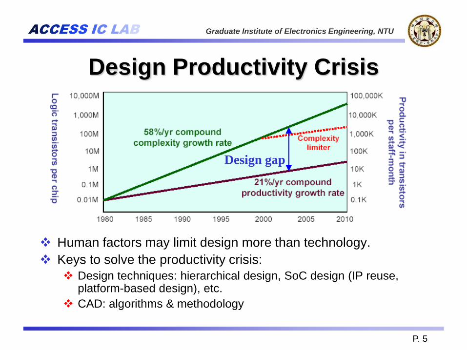
Design Productivity Crisis
Human factors may limit design more than technology.
Keys to solve the productivity crisis:
Design techniques: hierarchical design, SoC design (IP reuse, platform-based design), etc.
CAD: algorithms & methodology
Design gap
ACCESS IC LAB Graduate Institute of Electronics Engineering, NTU
P. 6
Increasing Processing Power
Very high performance circuits in today’s technologies. Gate delays: ~27ps for a 2-input Nand in CU11
Operating frequencies:
Up to 500MHz for SoC/Asic
Over 1GHz for custom designs
The increase in speed/performance of circuits allowed blocks to be reused without having to be redesigned and tuned for each application.
Enhanced Design Tools and Techniques Although not enough to close the “design gap”, tools are
essential for the design of today’s high-performance chips

ACCESS IC LAB Graduate Institute of Electronics Engineering, NTU
P. 7
IP / Cores Soft IP/Core Delivered as RTL verilog or VHDL source code with
synthesis script
Customers are responsible for synthesis, timing closure, and all front-end processing
Firm IP/Core Delivered as a netlist to be included in customer’s netlist
(with don't touch attribute)
Possibly with placement information
Hard IP/Core Due to their complexity, they are provided as a blackbox
(GDSII). Ex. Processors, analog cores, PLLs
Usually very tight timing constraints. Internal views not be alterable or visible to the customer

ACCESS IC LAB Graduate Institute of Electronics Engineering, NTU
P. 8
Changes in the Nature of IC Design
(IEEE Spectrum Nov,1996)

ACCESS IC LAB Graduate Institute of Electronics Engineering, NTU
P. 9
Chasing the Design Gap

ACCESS IC LAB Graduate Institute of Electronics Engineering, NTU
P. 10
Evolution of Silicon Design
Source: “Surviving the SoC revolution – A Guide to Platform-based Design,”
Henry Chang et al, Kluwer Academic Publishers, 1999

ACCESS IC LAB Graduate Institute of Electronics Engineering, NTU
P. 11
Methodology – Analysis and Verification

ACCESS IC LAB Graduate Institute of Electronics Engineering, NTU
P. 12
Outline
Introduction to Integrated Circuit
IC Design Flow
Verilog HDL concept
Verilog Simulator

ACCESS IC LAB Graduate Institute of Electronics Engineering, NTU
P. 13
IC Design and ImplementationIdea
Design

ACCESS IC LAB Graduate Institute of Electronics Engineering, NTU
FPGA Design Flow(1/3)
P. 14

ACCESS IC LAB Graduate Institute of Electronics Engineering, NTU
FPGA Design Flow(2/3)
Architecture design. This stage involves analysis of the project
requirements, problem decomposition and functional simulation
(if applicable).
HDL design entry. The device is described in a formal
hardware description language (HDL). The most common HDLs
are VHDL and Verilog.
Test environment design. This stage involves writing of test
environments and behavioral models (when applicable) to
ensure that the HDL description of a device is correct.
Behavioral simulation. This is an important stage that checks
HDL correctness by comparing outputs of the HDL model and
the behavioral model.
P. 15

ACCESS IC LAB Graduate Institute of Electronics Engineering, NTU
FPGA Design Flow(3/3)
Synthesis. This stage involves conversion of an HDL
description to a so-called netlist which is basically a formally
written digital circuit schematic. Synthesis is performed by a
special software called synthesizer.
Implementation. A synthesizer-generated netlist is mapped
onto particular device's internal structure. The main phase of the
implementation stage is place and route or layout, which
allocates FPGA resources. Then these configuration data are
written to a special file by a program called bitstream generator.
Timing analysis. Checks whether the implemented design
satisfies timing constraints specified by the user.
P. 16

ACCESS IC LAB Graduate Institute of Electronics Engineering, NTU
P. 17
IC Design Flow
Design Specification
Design Partition
Design Entry-Verilog
Behavioral Modeling
Simulation/Functional
Verification
Design Integration &
Verification
Pre-Synthesis
Sign-Off
Synthesize and Map
Gate-Level Netlist
Post-Synthesis
Design Validation
Post-Synthesis
Timing Verification
Test Generation &
Fault Simulation
Cell Placement, Scan
Chain & Clock Tree
Insertion, Cell Routing
Verify Physical &
Electrical Design Rules
Extract Parasitics
Post-Layout
Timing Verification
Production-Ready
MasksFront End
Design Sign-Off
Back End

ACCESS IC LAB Graduate Institute of Electronics Engineering, NTU
Summary
They have the same front end design, but different back
end design
IC design
The fundamental cell is transistor
The communication of transistor is based on mask
Real chip
Need long time to tape out
FPGA
The fundamental cell is logic cell
The communication of transistor is based on programming approach
Real board
Easy to implement
P. 18

ACCESS IC LAB Graduate Institute of Electronics Engineering, NTU
P. 19
Outline
Introduction to Integrated Circuit
IC Design Flow
Verilog HDL concept
Verilog Simulator

ACCESS IC LAB Graduate Institute of Electronics Engineering, NTU
P. 20
Introduction to HDL
HDL – Hardware Description Language
Why use an HDL ?
Hardware is becoming very difficult to design
directly
HDL is easier and cheaper to explore different
design options
Reduce time and cost

ACCESS IC LAB Graduate Institute of Electronics Engineering, NTU
P. 21
Verilog HDL
Features
HDL has high-level programming language
constructs and constructs to describe the
connectivity of your circuit.
Ability to mix different levels of abstraction freely
One language for all aspects of design, test, and
verification
Functionality as well as timing
Concurrency perform
Support timing simulation

ACCESS IC LAB Graduate Institute of Electronics Engineering, NTU
P. 22
Compared to VHDL
Verilog and VHDL are comparable languages
VHDL has a slightly wider scope System-level modeling
Exposes even more discrete-event machinery
VHDL is better-behaved Fewer sources of non-determinism
(e.g., no shared variables ???)
VHDL is harder to simulate quickly
VHDL has fewer built-in facilities for hardware modeling
VHDL is a much more verbose languageMost examples don’t fit on slides

ACCESS IC LAB Graduate Institute of Electronics Engineering, NTU
P. 23
The Verilog Language
Originally a modeling language
for a very efficient event-driven digital logic simulator
Later pushed into use as a specification language
for logic synthesis
Now, one of the two most commonly-used languages
in digital hardware design (VHDL is the other)
Combines structural and behavioral modeling styles
ACCESS IC LAB Graduate Institute of Electronics Engineering, NTU
P. 24
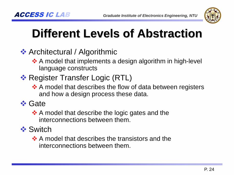
Different Levels of Abstraction
Architectural / Algorithmic A model that implements a design algorithm in high-level
language constructs
Register Transfer Logic (RTL) A model that describes the flow of data between registers
and how a design process these data.
Gate A model that describe the logic gates and the
interconnections between them.
Switch A model that describes the transistors and the
interconnections between them.

ACCESS IC LAB Graduate Institute of Electronics Engineering, NTU
P. 25
Verilog HDL Behavior Language
Structural and procedural like the C programming
language
Used to describe algorithm level and RTL level
Verilog models
Key features
Procedural constructs for conditional, if-else, case, and
looping operations.
Arithmetic, logical, bit-wise, and reduction operations for
expressions.
Timing control.

ACCESS IC LAB Graduate Institute of Electronics Engineering, NTU
P. 26
Verilog HDL Structural Language
Used to describe gate-level and switch-level
circuits.
Key features
A complete set set of combinational primitives
Support primitive gate delay specification
Support primitive gate output strength
specification

ACCESS IC LAB Graduate Institute of Electronics Engineering, NTU
P. 27
Language Conventions (1/2)
Case-sensitivity
Verilog is case-sensitive.
Some simulators are case-insensitive
Advice: - Don’t use case-sensitive feature!
Keywords are lower case
Different names must be used for different items within the same scope
Identifier alphabet:
Upper and lower case alphabeticals: a~z A~Z
Decimal digits: 0~9
Underscore: _
ACCESS IC LAB Graduate Institute of Electronics Engineering, NTU
P. 28
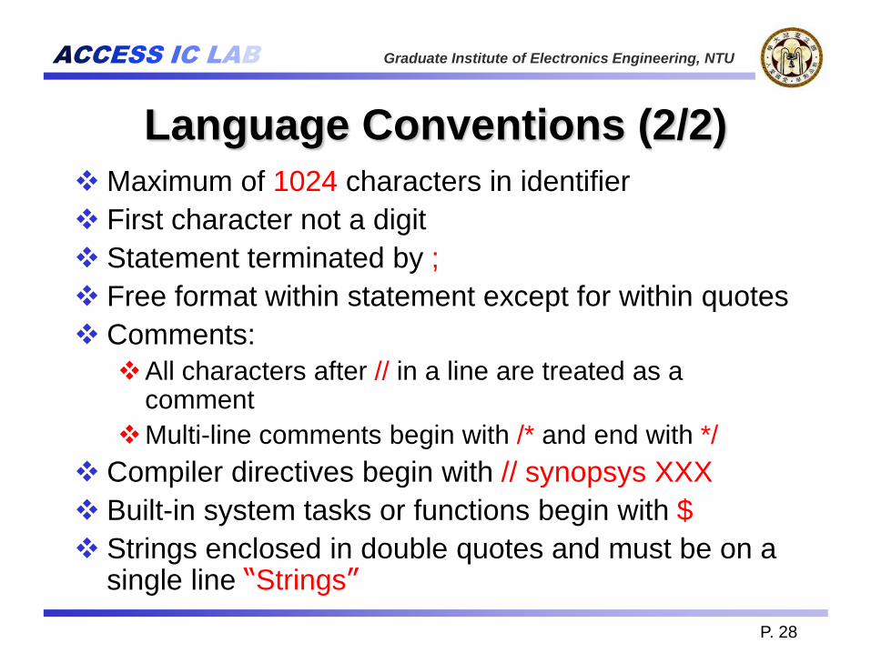
Language Conventions (2/2)
Maximum of 1024 characters in identifier
First character not a digit
Statement terminated by ;
Free format within statement except for within quotes
Comments:
All characters after // in a line are treated as a comment
Multi-line comments begin with /* and end with */
Compiler directives begin with // synopsys XXX
Built-in system tasks or functions begin with $
Strings enclosed in double quotes and must be on a single line “Strings”

ACCESS IC LAB Graduate Institute of Electronics Engineering, NTU
P. 29
Design Encapsulation
Encapsulate structural and functional details in a module
Encapsulation makes the model available for instantiation in
other modules
module my_design (ports_list);
... // Declarations of ports go here
... // Structural and functional details go here
endmodule

ACCESS IC LAB Graduate Institute of Electronics Engineering, NTU
P. 30
Port Declaration
Three port types
Input port
input a;
Output port
output b;
Bi-direction port
inout c;
net
net
netnet
input output
inout
reg or net reg or net
module
Port list
Port Declaration
module full_add (S, CO, A, B, CI) ;
output S, CO ;input A, B, CI ;
--- function description ---
endmodule

ACCESS IC LAB Graduate Institute of Electronics Engineering, NTU
P. 31
Two Main Data Types
Nets represent connections between things Do not hold their value
Take their value from a driver such as a gate or other module
Cannot be assigned in an initial or always block
Regs represent data storage Behave exactly like memory in a computer
Hold their value until explicitly assigned in an initial or always block
Never connected to something
Can be used to model latches, flip-flops, etc., but do not correspond exactly
Shared variables with all their attendant problems

ACCESS IC LAB Graduate Institute of Electronics Engineering, NTU
P. 32
Primitive Cells
Primitives are simple modules
Verilog build-in primitive gate not, buf:
Variable outputs, single input (last port)
and, or, buf, xor, nand, nor, xnor:
Single outputs (first port), variable inputs
module full_add (S, CO, A, B, CI) ;--- port Declaration ---wire net1, net2, net3;xor U0(S,A,B,CI);and U1(net1, A, B);and U2(net2, B, CI);and U3(net3, CI, A);or U4(CO, net1, net2, net3);
endmodule

ACCESS IC LAB Graduate Institute of Electronics Engineering, NTU
P. 33
How Are Simulators Used?
Testbench generates stimulus and checks response
Coupled to model of the system
Pair is run simultaneously
Testbench System Model
Stimulus
ResponseResult checker
ACCESS IC LAB Graduate Institute of Electronics Engineering, NTU
P. 34
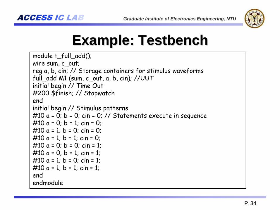
Example: Testbenchmodule t_full_add();wire sum, c_out;reg a, b, cin; // Storage containers for stimulus waveformsfull_add M1 (sum, c_out, a, b, cin); //UUTinitial begin // Time Out#200 $finish; // Stopwatchendinitial begin // Stimulus patterns#10 a = 0; b = 0; cin = 0; // Statements execute in sequence#10 a = 0; b = 1; cin = 0; #10 a = 1; b = 0; cin = 0; #10 a = 1; b = 1; cin = 0; #10 a = 0; b = 0; cin = 1; #10 a = 0; b = 1; cin = 1; #10 a = 1; b = 0; cin = 1; #10 a = 1; b = 1; cin = 1;endendmodule

ACCESS IC LAB Graduate Institute of Electronics Engineering, NTU
P. 35
Outline
Introduction to Integrated Circuit
IC Design Flow
Verilog HDL concept
Verilog Simulator
ACCESS IC LAB Graduate Institute of Electronics Engineering, NTU
P. 36
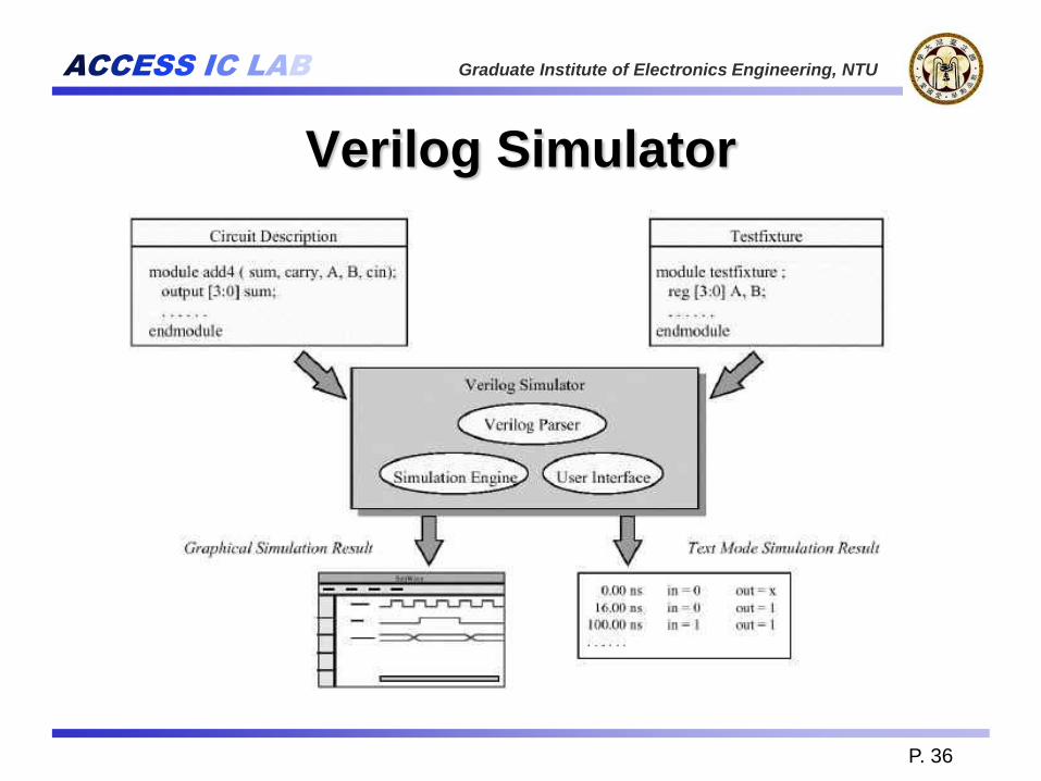
Verilog Simulator
ACCESS IC LAB Graduate Institute of Electronics Engineering, NTU
P. 37
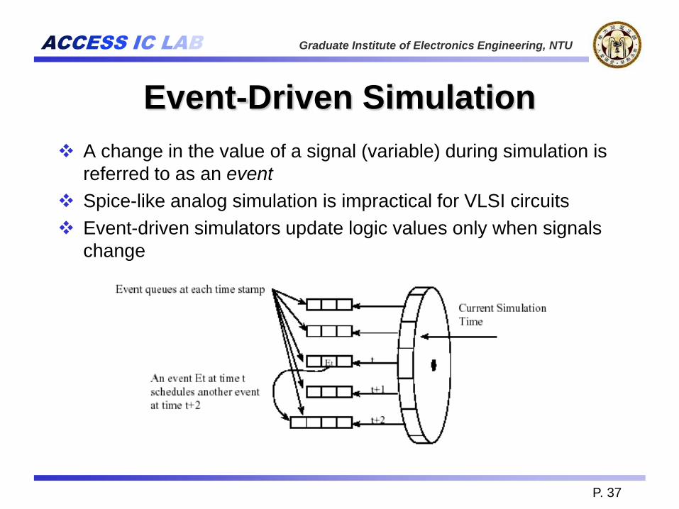
Event-Driven Simulation
A change in the value of a signal (variable) during simulation is
referred to as an event
Spice-like analog simulation is impractical for VLSI circuits
Event-driven simulators update logic values only when signals
change

ACCESS IC LAB Graduate Institute of Electronics Engineering, NTU
P. 38
Styles
Structural - instantiation of primitives and
modules
RTL/Dataflow - continuous assignments
Behavioral - procedural assignments

ACCESS IC LAB Graduate Institute of Electronics Engineering, NTU
P. 39
Structural Modeling
When Verilog was first developed (1984)
most logic simulators operated on netlists
Netlist: list of gates and how they’re
connected
A natural representation of a digital logic
circuit
Not the most convenient way to express test
benches

ACCESS IC LAB Graduate Institute of Electronics Engineering, NTU
P. 40
Behavioral Modeling
A much easier way to write testbenches
Also good for more abstract models of circuits
Easier to write
Simulates faster
More flexible
Provides sequencing
Verilog succeeded in part because it allowed
both the model and the testbench to be
described together

ACCESS IC LAB Graduate Institute of Electronics Engineering, NTU
P. 41
Style 1 - Structural
module full_add (S, CO, A, B, CI) ;
output S, CO ;input A, B, CI ;
wire N1, N2, N3;
half_add HA1 (N1, N2, A, B),HA2 (S, N3, N1, CI);
or P1 (CO, N3, N2);
endmodule
module half_add (S, C, X, Y);
output S, C ;input X, Y ;
xor (S, X, Y) ;and (C, X, Y) ;
endmodule
ACCESS IC LAB Graduate Institute of Electronics Engineering, NTU
P. 42
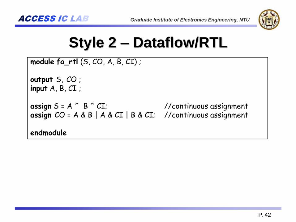
Style 2 – Dataflow/RTLmodule fa_rtl (S, CO, A, B, CI) ;
output S, CO ;input A, B, CI ;
assign S = A ^ B ^ CI; //continuous assignmentassign CO = A & B | A & CI | B & CI; //continuous assignment
endmodule
ACCESS IC LAB Graduate Institute of Electronics Engineering, NTU
P. 43
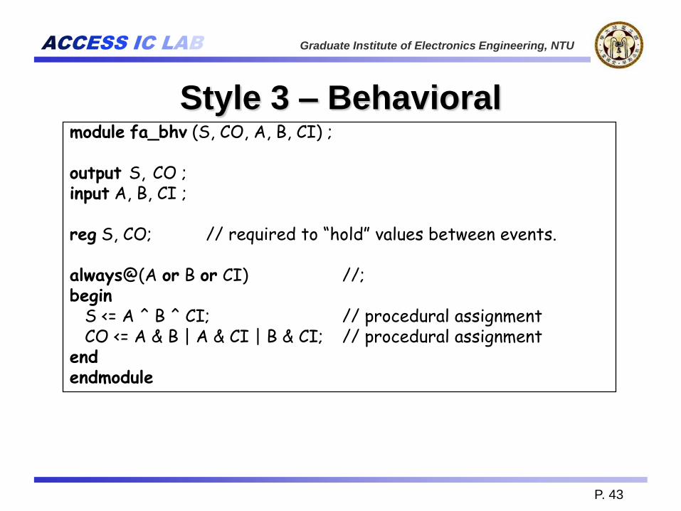
Style 3 – Behavioralmodule fa_bhv (S, CO, A, B, CI) ;
output S, CO ;input A, B, CI ;
reg S, CO; // required to “hold” values between events.
always@(A or B or CI) //; begin
S <= A ^ B ^ CI; // procedural assignmentCO <= A & B | A & CI | B & CI; // procedural assignment
end endmodule

ACCESS IC LAB Graduate Institute of Electronics Engineering, NTU
P. 44
How Verilog Is Used
Virtually every ASIC is designed using either Verilog
or VHDL (a similar language)
Behavioral modeling with some structural elements
“Synthesis subset”
Can be translated using Synopsys’ Design Compiler or
others into a netlist
Design written in Verilog
Simulated to death to check functionality
Synthesized (netlist generated)
Static timing analysis to check timing

ACCESS IC LAB Graduate Institute of Electronics Engineering, NTU
P. 45
Verilog-HDL Simulators
Xilinx ISE
Mentor Graphics ModelSim
http://www.mentor.com/
Cadence Verilog-XL
NC-Verilog
Related Documents