972 IEEE TRANSACTIONS ON COMPUTER-AIDED DESIGN OF INTEGRATED CIRCUITS AND SYSTEMS, VOL. 34, NO. 6, JUNE 2015 Managing Laser Power in Silicon-Photonic NoC Through Cache and NoC Reconfiguration Chao Chen, Member, IEEE, José L. Abellán, Member, IEEE, and Ajay Joshi, Member, IEEE Abstract—In manycore systems, the silicon-photonic link tech- nology is projected to replace electrical link technology for global communication in network-on-chip (NoC) as it can pro- vide as much as an order of magnitude higher bandwidth density and lower data-dependent power. However, a large amount of fixed power is dissipated in the laser sources required to drive these silicon-photonic links, which negates any bandwidth den- sity advantages. This large laser power dissipation depends on the number of on-chip silicon-photonic links, the bandwidth of each link, and the photonic losses along each link. In this paper, we propose to reduce the laser power dissipation at run- time by dynamically activating/deactivating L2 cache banks and switching ON/OFF the corresponding silicon-photonic links in the NoC. This method effectively throttles the total on-chip NoC bandwidth at runtime according to the memory access features of the applications running on the manycore system. Full-system simulation utilizing Princeton application repository for shared-memory computers and Stanford parallel applica- tions for shared-memory-2 parallel benchmarks reveal that our proposed technique achieves on an average 23.8% (peak value 74.3%) savings in laser power, and 9.2% (peak value 26.9%) lower energy-delay product for the whole system at the cost of 0.65% loss (peak value 2.6%) in instructions per cycle on aver- age when compared to the cases where all L2 cache banks are always active. Index Terms—Laser power management, manycore systems, network-on-chip (NoC) reconfiguration, silicon-photonic NoC. I. I NTRODUCTION T ODAY’S manycore systems have tens of cores on a single chip. In the future, this core count is expected to grow into the hundreds (maybe even thousands). This ever-increasing core count has made it necessary to design a shared network-on-chip (NoC) medium for on-chip com- munication. The manycore systems that are commercially available today [1]–[3] use a mesh topology. The choice of this low-radix high-diameter mesh topology is driven by the fact that a mesh network requires short interconnects and Manuscript received August 6, 2014; revised November 11, 2014; accepted January 27, 2015. Date of publication February 10, 2015; date of current version May 20, 2015. This work was supported by the National Science Foundation CAREER Award CCF-1149549. This paper was recommended by Associate Editor L. P. Carloni. C. Chen is with the Digital Networking Group, Freescale Semiconductor, Inc., Austin, TX 78735 USA (e-mail: [email protected]). J. L. Abellán is with the Department of Computer Science, Catholic University of Murcia, Murcia 30107, Spain. A. Joshi is with the Department of Electrical and Computer Engineering, Boston University, Boston, MA 02215 USA. This work was done when C. Chen was a Ph.D. student at Boston University. Color versions of one or more of the figures in this paper are available online at http://ieeexplore.ieee.org. Digital Object Identifier 10.1109/TCAD.2015.2402172 energy-efficient short interconnects can be easily designed using repeater-inserted electrical link technology. However, the mesh topology, due to its multihop packet transmission, requires the programmer to carefully map an application across several cores to extract maximum performance from a many- core architecture. A single-stage high-radix topology, such as a crossbar, reduces this extra effort required for mapping of threads. However, the implementation of a crossbar using elec- trical link technology for systems with large core counts is expensive in terms of energy and area. Silicon-photonic link technology has been proposed as a potential replacement to the electrical link technology in the design of the high-radix NoC of manycore systems [4]–[7]. The silicon-photonic link technology can provide an order of magnitude higher bandwidth density through dense wave- length division multiplexing [4]. Moreover, the data-dependent power in a silicon-photonic link is independent of the link length. Hence, it is possible to design a high-radix topol- ogy with long global interconnects using silicon-photonic link technology for the NoC. However, the fixed power dissipated in the laser source that is required to drive the silicon-photonic links can be nontrivial. Depending on the physical layout of the NoC and the materials used for the photonic devices, the fixed power in the laser source can more than offset the band- width density and data-dependent power advantages of the silicon-photonic link technology [4], [8], [9]. To enable an energy-efficient design of high-radix topolo- gies using silicon-photonic link technology for NoC, we need to develop techniques for lowering laser power dissipation. The applications running on the manycore systems typically exhibit spatial variations and/or temporal variations in the opti- mal NoC bandwidth requirements, optimal L1/L2 cache size requirements and optimal core count requirements. This cre- ates an opportunity for proactively reconfiguring the overall system architecture at runtime to minimize the power dissi- pated in the laser source. In this paper, we propose a run-time methodology to proactively control the size of the shared L2 cache and, in turn, the bandwidth of the NoC (between pri- vate L1 and shared L2 cache banks) to manage the power dissipated in the laser source. Our methodology periodically samples the L2 cache replacement rate to make a decision on increasing/decreasing the number of active L2 cache banks while ensuring a minimal change in the system performance. A decision to reduce the L2 cache bank count creates an oppor- tunity to switch OFF the silicon-photonic links associated with the deactivated L2 cache banks and, in turn, save laser power. The key idea here is to provide the minimum-sized L2 cache 0278-0070 c 2015 IEEE. Personal use is permitted, but republication/redistribution requires IEEE permission. See http://www.ieee.org/publications_standards/publications/rights/index.html for more information.

Welcome message from author
This document is posted to help you gain knowledge. Please leave a comment to let me know what you think about it! Share it to your friends and learn new things together.
Transcript

972 IEEE TRANSACTIONS ON COMPUTER-AIDED DESIGN OF INTEGRATED CIRCUITS AND SYSTEMS, VOL. 34, NO. 6, JUNE 2015
Managing Laser Power in Silicon-Photonic NoCThrough Cache and NoC Reconfiguration
Chao Chen, Member, IEEE, José L. Abellán, Member, IEEE, and Ajay Joshi, Member, IEEE
Abstract—In manycore systems, the silicon-photonic link tech-nology is projected to replace electrical link technology forglobal communication in network-on-chip (NoC) as it can pro-vide as much as an order of magnitude higher bandwidth densityand lower data-dependent power. However, a large amount offixed power is dissipated in the laser sources required to drivethese silicon-photonic links, which negates any bandwidth den-sity advantages. This large laser power dissipation depends onthe number of on-chip silicon-photonic links, the bandwidthof each link, and the photonic losses along each link. In thispaper, we propose to reduce the laser power dissipation at run-time by dynamically activating/deactivating L2 cache banks andswitching ON/OFF the corresponding silicon-photonic links inthe NoC. This method effectively throttles the total on-chipNoC bandwidth at runtime according to the memory accessfeatures of the applications running on the manycore system.Full-system simulation utilizing Princeton application repositoryfor shared-memory computers and Stanford parallel applica-tions for shared-memory-2 parallel benchmarks reveal that ourproposed technique achieves on an average 23.8% (peak value74.3%) savings in laser power, and 9.2% (peak value 26.9%)lower energy-delay product for the whole system at the cost of0.65% loss (peak value 2.6%) in instructions per cycle on aver-age when compared to the cases where all L2 cache banks arealways active.
Index Terms—Laser power management, manycore systems,network-on-chip (NoC) reconfiguration, silicon-photonic NoC.
I. INTRODUCTION
TODAY’S manycore systems have tens of cores on asingle chip. In the future, this core count is expected
to grow into the hundreds (maybe even thousands). Thisever-increasing core count has made it necessary to designa shared network-on-chip (NoC) medium for on-chip com-munication. The manycore systems that are commerciallyavailable today [1]–[3] use a mesh topology. The choice ofthis low-radix high-diameter mesh topology is driven by thefact that a mesh network requires short interconnects and
Manuscript received August 6, 2014; revised November 11, 2014; acceptedJanuary 27, 2015. Date of publication February 10, 2015; date of currentversion May 20, 2015. This work was supported by the National ScienceFoundation CAREER Award CCF-1149549. This paper was recommendedby Associate Editor L. P. Carloni.
C. Chen is with the Digital Networking Group, Freescale Semiconductor,Inc., Austin, TX 78735 USA (e-mail: [email protected]).
J. L. Abellán is with the Department of Computer Science, CatholicUniversity of Murcia, Murcia 30107, Spain.
A. Joshi is with the Department of Electrical and Computer Engineering,Boston University, Boston, MA 02215 USA.
This work was done when C. Chen was a Ph.D. student at BostonUniversity.
Color versions of one or more of the figures in this paper are availableonline at http://ieeexplore.ieee.org.
Digital Object Identifier 10.1109/TCAD.2015.2402172
energy-efficient short interconnects can be easily designedusing repeater-inserted electrical link technology. However,the mesh topology, due to its multihop packet transmission,requires the programmer to carefully map an application acrossseveral cores to extract maximum performance from a many-core architecture. A single-stage high-radix topology, such asa crossbar, reduces this extra effort required for mapping ofthreads. However, the implementation of a crossbar using elec-trical link technology for systems with large core counts isexpensive in terms of energy and area.
Silicon-photonic link technology has been proposed as apotential replacement to the electrical link technology in thedesign of the high-radix NoC of manycore systems [4]–[7].The silicon-photonic link technology can provide an orderof magnitude higher bandwidth density through dense wave-length division multiplexing [4]. Moreover, the data-dependentpower in a silicon-photonic link is independent of the linklength. Hence, it is possible to design a high-radix topol-ogy with long global interconnects using silicon-photonic linktechnology for the NoC. However, the fixed power dissipatedin the laser source that is required to drive the silicon-photoniclinks can be nontrivial. Depending on the physical layout ofthe NoC and the materials used for the photonic devices, thefixed power in the laser source can more than offset the band-width density and data-dependent power advantages of thesilicon-photonic link technology [4], [8], [9].
To enable an energy-efficient design of high-radix topolo-gies using silicon-photonic link technology for NoC, we needto develop techniques for lowering laser power dissipation.The applications running on the manycore systems typicallyexhibit spatial variations and/or temporal variations in the opti-mal NoC bandwidth requirements, optimal L1/L2 cache sizerequirements and optimal core count requirements. This cre-ates an opportunity for proactively reconfiguring the overallsystem architecture at runtime to minimize the power dissi-pated in the laser source. In this paper, we propose a run-timemethodology to proactively control the size of the shared L2cache and, in turn, the bandwidth of the NoC (between pri-vate L1 and shared L2 cache banks) to manage the powerdissipated in the laser source. Our methodology periodicallysamples the L2 cache replacement rate to make a decisionon increasing/decreasing the number of active L2 cache bankswhile ensuring a minimal change in the system performance. Adecision to reduce the L2 cache bank count creates an oppor-tunity to switch OFF the silicon-photonic links associated withthe deactivated L2 cache banks and, in turn, save laser power.The key idea here is to provide the minimum-sized L2 cache
0278-0070 c© 2015 IEEE. Personal use is permitted, but republication/redistribution requires IEEE permission.See http://www.ieee.org/publications_standards/publications/rights/index.html for more information.

CHEN et al.: MANAGING LASER POWER IN SILICON-PHOTONIC NoC THROUGH CACHE AND NoC RECONFIGURATION 973
(i.e., the minimum number of L2 cache banks) and the min-imum NoC bandwidth (i.e., the minimum number of activesilicon-photonic links) required for an application to achievethe maximum possible performance at any given point of time.The main contributions of this paper are as follows.
1) We propose a policy for run-time management of powerdissipated in the laser source that drives a crossbarNoC that connects the private L1 caches and the dis-tributed shared L2 cache banks. At runtime, using theL2 cache replacement rate metric, we determine therequired change in the L2 cache bank count and hencethe number of silicon-photonic links to maximize appli-cation performance and minimize laser power, whichin turn maximizes the energy efficiency of the overallsystem.
2) We evaluate our laser power management policy usinga 64-core system with silicon-photonic crossbar NoC asthe target system. For evaluation, we use the Gem5 [10]simulator and princeton application repository forshared-memory computers (PARSEC) [11] and stanfordparallel applications for shared-memory (SPLASH)-2 [12] parallel benchmark suites. In our analysis, wecompare two different versions of the target system—asystem that uses our laser management policy to recon-figure the L2 cache and the NoC, and a system thatkeeps the entire L2 cache and the NoC ON all the time.On average, our proposed approach saves laser power by23.8% (peak value 74.3%) and system power by 9.9%(peak value 30.6%), with instructions per cycle (IPC)degradation of 0.65% (peak value 2.6%), and energy-delay product (EDP) improvement by 9.2% (peak value26.9%).
The rest of this paper is organized as follows. We describethe related work in Section II followed by the detailed architec-ture of our target system in Section III. We present an overviewof the silicon-photonic link technology in Section IV followedby a detailed discussion of our proposed runtime cache andNoC reconfiguration methodology in Section V. We presentthe evaluation of our proposed approach for laser power man-agement in Section VI. This is followed by a discussion ofthe application of our methodology to alternate cache archi-tectures, systems with large core counts, and alternate NoCtopologies in Section VII. Finally, Section VIII summarizesthe main conclusion of this paper.
II. RELATED WORK
The silicon-photonic link technology has been widelyexplored to implement the entire spectrum of net-work topologies—from low-radix high-diameter mesh/torustopologies [7], [13] to medium-radix medium-diameterbutterfly/crossbar topologies [4], [6], [14] to high-radix low-diameter bus/crossbar topologies [5], [15]. A general consensusamong the various efforts so far is that silicon-photonic net-works provide a bandwidth density and data-dependent poweradvantage for NoC communication. However, the fixed amountof power dissipated in the laser sources that drive the silicon-photonic NoC negates these advantages. Hence, to enable the
use of silicon-photonic NoC in future manycore systems, weneed to develop techniques to proactively manage laser power.
The standard design-time device-level solutions to reduceoptical loss in silicon-photonic devices, and in turn reducethe laser power range from exploring different materials toprocess flows to device geometries. At the circuit level,novel receiver circuits can be designed to operate with low-sensitivity photodetectors or one can lower the power injectedinto the silicon-photonic links and any resulting errors canbe detected/corrected using coding techniques. At the archi-tecture level, a nanophotonic crossbar architecture that usesoptical channel sharing to manage static power dissipation isproposed in [16]. Here, a token-stream mechanism is usedfor channel arbitration and credit distribution, to enable effi-cient global sharing of crossbar channels. Zhou and Kodi [17]proposed to use a prediction mechanism to dynamically scalethe NoC bandwidth depending on the demands of the overly-ing application and in turn reduce optical power dissipation.Li et al. [18] proposed to divide the photonic NoC into sub-nets and share photonic channels for sending arbitration anddata packets to reduce laser power. Chen and Joshi [19] pro-posed to use weighted time-division multiplexing to distributethe laser power across multiple photonic links based on theruntime variations in the bandwidth requirements within andacross applications to maximize energy efficiency.
We propose to manage the laser power dissipated in thesilicon-photonic NoC between the private L1 caches anddistributed shared L2 cache banks through NoC and cachereconfiguration. In our approach, we determine the minimumnumber of L2 cache banks that is required to maximize theapplication performance. The extra L2 cache banks are deac-tivated and the silicon-photonic links associated with thoseL2 cache banks are switched OFF to save laser power. Theidea of reconfiguring the cache architecture to reduce cacheenergy and/or improve performance has been explored in thepast [20], [21]. However, it has never been used to managethe power dissipated in a silicon-photonic NoC. The main goalhere is to minimize the EDP of the overall manycore system byleveraging the spatial and temporal variations in the behaviorof the applications.
III. TARGET SYSTEM
We choose a 64-core processor that is manufactured using22-nm CMOS technology as our target system. However, itshould be noted that our proposed technique for laser powermanagement can easily scale with core count. Our target sys-tem is a 3-D system, where the logic layer contains the CMOSlogic and monolithically integrated photonic devices, while thelaser layer contains the laser sources. The cores in the logiclayer are configured based on the cores used in Intel’s 48-coreSCC [1]. The micro-architectural parameters of the target sys-tem are listed in Table I. The target system has a total of4 MB L2 cache. This size was determined by running all ourtarget benchmark applications and determining the minimumL2 cache size that maximizes performance of the applicationsthat we have used for evaluation. Alternate set of applicationscould indicate the need for larger L2 cache sizes. However,

974 IEEE TRANSACTIONS ON COMPUTER-AIDED DESIGN OF INTEGRATED CIRCUITS AND SYSTEMS, VOL. 34, NO. 6, JUNE 2015
TABLE ISIXTY-FOUR CORE TARGET SYSTEM PARAMETERS
Fig. 1. Logical view of a silicon-photonic crossbar network between 64cores (each with a private L1 cache) and 8 L2 cache banks. The crossbaruses SWMR for L2-to-L1 communication and MWSR for L1-to-L2 commu-nication. Each ring shown in the figure represents a set of 64 ring modulatorsand 64 ring filters for data channels with a few extra rings for token andreservation channels.
our proposed technique of laser power management using L2cache and NoC reconfiguration would still be applicable.
For on-chip communication, we consider a high-radix cross-bar NoC architecture (see Fig. 1). The NoC employs themultiple-write-single-read (MWSR) mechanism for L1-to-L2communication with a dedicated silicon-photonic channel hav-ing a width of 512 bits for each L2 cache bank. A token-basedprotocol is used to arbitrate between the L1 caches for gettingaccess to L1-to-L2 communication channels [5]. Tokens areassigned in a round-robin fashion for fairness. The networkemploys the single-write-multiple-read (SWMR) mechanismfor L2-to-L1 communication with a dedicated silicon-photonicchannel having a width of 512 bits for each L2 cache bank.The reservation channel is used to enable the ring filters at tar-geted destination L1 caches before an L2 cache bank transmitspackets onto the L2-to-L1 data channels [16]. Each logicallink in Fig. 1 represents one L1-to-L2 MWSR data channel(with corresponding token channel) and one L2-to-L1 SWMRdata channel (with corresponding reservation channel). Eachring shown in Fig. 1 represents a set of 64 ring modulatorsand 64 ring filters for data channels (with few extra rings for
Fig. 2. Physical layout of the silicon-photonic crossbar NoC between 64cores (each with a private L1 cache) and eight L2 cache banks. The L2cache banks are located at the ends of the silicon-photonic links for ease ofarbitration. The reconfiguration controller (RC) is placed in the center of theL2 caches and the laser sources are placed right above the RC and L2 cachesto minimize the reconfiguration overhead.
token and reservations). This approach of using MWSR mech-anism for L1-to-L2 communication and SWMR for L2-to-L1communication where all the communication associated withan L2 cache bank is mapped onto dedicated silicon-photoniclinks provides the opportunity to easily switch OFF/ON thesededicated silicon-photonic links when the L2 cache bank isdeactivated/activated.
Fig. 2 shows the physical layout of the silicon-photonicnetwork between 64 private L1 caches and eight shared anddistributed L2 cache banks. Cache lines are interleaved acrossL2 cache banks to enable the parallel accessibility. We usea modified exclusive shared invalid (MESI) directory-basedprotocol for maintaining cache coherency between L1 andL2 cache banks. The cache coherency directories are locatednext to the associated L2 cache banks. Any core-to-core com-munication is through the directory, hence no forward-typecoherency messages are implemented. The L2 cache banksand memory controllers (MCs) are co-located on the edge ofthe processor; therefore L2 cache banks can access all theMCs through local wiring upon L2 cache misses. In the phys-ical layout, the waveguides are routed in a U-shape layout.Instead of the conventional off-chip laser sources, we opt foron-chip laser sources because they can be quickly switchedON/OFF to correspondingly switch ON/OFF the associatedsilicon-photonic links (more details in Section IV). The lasersources are placed in a separate layer above the low powerdensity L2 caches to minimize the impact of power dissipatedin the logic layer on the laser source temperature. Here, thelaser sources are placed along one edge of the chip but otherarrangements are also feasible [22].
There is a separate off-chip photonic network that con-nects MCs to PIDRAM chips [23]. We assume an averagetime of 50 ns for the round-trip delay between the MCs andPIDRAMs. We ignore the variations in queuing latencies atthe inputs of MCs because the high off-chip bandwidth usingPIDRAM significantly reduces the number of outstandingmemory requests in the queue.
IV. PHOTONIC TECHNOLOGY
Silicon-photonic devices can be interfaced with conven-tional CMOS devices using monolithic integration or 3-D

CHEN et al.: MANAGING LASER POWER IN SILICON-PHOTONIC NoC THROUGH CACHE AND NoC RECONFIGURATION 975
Fig. 3. Photonic link components. Two point-to-point photonic linksimplemented with WDM.
integration. Monolithic integration (using bulk CMOS processor SOI process) involves using the existing layers in the pro-cess technology to design photonic devices. On the other hand,3-D integration involves integrating an SOI chip of a differentprocess or depositing custom photonic layers (SiN or poly-crystalline silicon) above the metal layers and interfacing theCMOS devices and photonic devices through vias. Our pro-posed technique for using cache and NoC reconfigurationfor managing laser power is applicable to silicon-photonicNoC designed using both monolithic integration and 3-D inte-gration. The percent of savings in laser power in the 3-Dintegration case would be same as the monolithic integrationcase. However, in case of 3-D integration the parasitics at theinterface of the optical layer and logic layer are very high, and,in turn, the E-O-E conversion cost would be very high mak-ing it infeasible for silicon-photonic NoC. Hence, we focus onusing monolithic integration and minimizing the laser powerto make the photonic NoC more energy efficient.
Fig. 3 shows a generic wavelength-division multi-plexed (WDM) photonic link used for intrachip communi-cation. Light waves of wavelength λ1 and λ2 emitted by alaser source are coupled into the chip using vertical gratingcouplers. These couplers allow for vertical coupling into pla-nar waveguides. These light waves pass next to a series ofring modulators controlled by modulator drivers based on thedata to be transmitted on the link. The modulators convertdata from the electrical domain to the photonic domain. Themodulated light waves propagate along the waveguide and canpass through zero or more ring filters. At the receiver side, thering filter “drops” the light wave having the filter’s resonantwavelength onto a photodetector. The resulting photodetectorcurrent is sensed by an electrical receiver. At this stage, datais converted back into the electrical domain from the photonicdomain.
For our analysis, we consider a silicon-photonic link designsimilar to that proposed in [4]. This link design uses double-ring filters with a 4 THz free-spectral range, which enablesup to 128λ modulated at 10 Gb/s on each waveguide (64 λ
in each direction, interleaved to alleviate filter roll-off require-ments and crosstalk). A nonlinearity limit of 30 mW at 1 dBloss is assumed for the waveguides. In our target system, thislimits the number of wavelengths per waveguide to 15 in ourproposed layout. The waveguides are single mode and havea pitch of 4 μm to minimize the crosstalk between neighbor-ing waveguides. Modulator ring and filter ring diameters are∼10 μm. The latency of the photonic link is assumed to be3 cycles (1 cycle in flight and 1 cycle each for electrical-to-optical and optical-to-electrical conversion) + serialization
TABLE IIPHOTONIC TECHNOLOGY PARAMETER VALUES BASED ON
MEASUREMENTS AND PROJECTIONS
latency + latency due to contention for NoC resources. We usethe measurement values of silicon-photonic links designed in45 nm SoI [24]–[27] and project those values to 22 nm SoItechnology (see Table II). As we scale CMOS technology from45 to 22 nm, the optical losses in photonic devices and thethermal tuning power per K will not change as these valuesdepend on the photonic device designs, which do not scaleas we scale CMOS transistors from 45 to 22 nm. For thermaltuning power calculations, we assume the rings have to betuned over a range of 10 K. We use fixed-voltage technologyscaling rules to determine the energy consumed in modula-tor driver circuit (for E-to-O conversion) and receiver circuit(for O-to-E conversion).
Over the past few years, several different on-chip lasersource technologies have been proposed [28]–[30]. Thesetechnologies require further development, but they can sim-plify packaging and improve the energy-efficiency of photonicNoCs. We employ multiple on-chip single-mode indium phos-phide (InP)-based laser sources for powering the waveguides.Integrated multiwavelength lasers [31] or comb lasers [32]could also be utilized in our target system. However, thesealternatives have a large footprint or require further technolog-ical development. Therefore, we consider a set of single-modelaser sources in this paper. We use dedicated laser sources foreach L2 to simplify the laser switch ON/OFF process. EachL2 bank requires 64 wavelengths each for L2-to-L1 communi-cation and L1-to-L2 communication. The 30 mW nonlinearitylimit restricts the number of wavelengths per waveguide to 15.Hence, a single waveguide is driven by 15 single band lasersource with each source emitting about 2 mW of opticalpower. In our target system, 1920 single band laser sources(300 × 50 μm each) occupy approximately 28 mm2 on thelaser layer. The laser source efficiency varies with temperatureand output optical power. For our (InP)-based laser sourcesthe efficiency can be as large as 10% if we can maintain thelaser temperature at 65 ◦C. In this paper, we use a projectedlaser source efficiency of 5%. A more detailed discussion ofthe laser source technology that we have used can be foundin [22]. It should be noted though that our proposed approachfor laser power management is also applicable to other on-chiplaser source technologies.

976 IEEE TRANSACTIONS ON COMPUTER-AIDED DESIGN OF INTEGRATED CIRCUITS AND SYSTEMS, VOL. 34, NO. 6, JUNE 2015
In our target system, the laser sources are placed on the lasersource layer on top of the logic layer. Compared with off-chiplaser sources, the on-chip laser sources are located closer tothe logic layer and have faster switch ON/OFF time. Sinceour power savings technique relies on switching ON/OFF thesilicon-photonic links associated with activated/deactivated L2cache banks, the on-chip laser ON/OFF characteristics are crit-ical for maximizing the benefits of our proposed technique.When the on-chip laser supply current is turned ON, both thecarrier density and photon density in the on-chip laser activemedium reach a steady-state condition rapidly (on the orderof ns [33]). The on-chip laser dissipates power in the form ofheat when turned ON, therefore some temperature stabiliza-tion time is required. However, considering all of these effects,on-chip semiconductor diode lasers have demonstrated stablepulses with pulse widths (time to switch ON/OFF the laser cur-rent) of 35 ns [34]. This switch ON/OFF time is suitable forour approach as we reconfigure the L2 cache every ten millioninstruction (which is approximately 500 μs for our target setof benchmarks running on the target system described earlier).And even if more precision were required to ensure power andlasing wavelength stability, a simple wavelength locking cir-cuit could be employed [35]. In this paper, we explore theapplication of our power management technique consideringon-chip laser source with switch ON/OFF times of 100 ns.
V. RUNTIME RECONFIGURATION
In this section, we describe our runtime cache and NoCreconfiguration technique that can reduce laser power whilesustaining performance. The key idea is to track the dynamicchanges in the size of an application’s working set duringdifferent phases of application execution and reconfigure theL2 cache bank count and NoC at runtime. Essentially, if theentire working set can fit into a smaller L2 cache, we cansave laser power by deactivating some L2 cache banks andtheir associated silicon-photonic links. On the other hand,if the working set requires a larger L2 capacity, we needto activate more L2 cache banks and their correspondingsilicon-photonic links to avoid excessive L2 cache missesand sustain application performance. It should be noted thatwe are not proposing a new L2 cache reconfiguration tech-nique. Several techniques have already been proposed forL2 cache reconfiguration [20], [21], [36], [37]. However, theuse of L2 cache reconfiguration to manage laser power insilicon-photonic NoC has never been explored before.
A. RC
We propose to use a RC that is responsible for tracking thevariations in the application working set size and making thedecisions on the required changes in the L2 cache bank count.As we will see, the decision on changing the L2 cache capac-ity relies on the L2 cache replacement rate that the RC mustcollect from the current set of L2 banks. The RC is locatedon the edge of the chip where the L2 cache banks and lasersources are also located (see Fig. 2). For each L2 bank, twosingle-bit point-to-point electrical channels are used: one tosend data from the L2 bank to the RC and the other to send
Fig. 4. Flowchart for activating/deactivating L2 cache banks and theassociated silicon-photonic links at runtime.
data from the RC to the L2 bank. The single-bit channel cantransmit the cache replacement rate of the L2 bank (a 32-bitfloating point value assuming the single-precision IEEE 754standard) toward the RC in 32 clock cycles (very small com-pared to the large sampling period). The RC employs anotherpair of unidirectional single-bit point-to-point electrical linksper laser source for communication. These electrical channelsused for communication between RC and L2, and between RCand laser sources have minimal energy and area overhead dueto their very low bandwidth and proximity to the RC.
Fig. 4 shows the flow chart of the reconfiguration processperformed by the RC. After each sampling period, to collectthe L2 cache replacement rate, the RC sends a 1-bit signaltoward every active L2 cache bank utilizing each banks’ asso-ciated electrical link. After one clock cycle, the L2 cachebank starts reporting back the L2 cache replacement rate.The RC collects all replacement rates in the next 32 clockcycles (32-bit floating point values transmitted through 1-bitelectrical links), and decides whether to increase/decrease thenumber of L2 cache banks and the number of active silicon-photonic links. In our system, the RC increases/decreases thenumber of L2 cache banks in powers of 2 as it is shown inFig. 5. Alternate granularities could be used in our approachfor increasing/decreasing the L2 cache size and hence the laserpower. However, that complicates the process of determiningthe home bank (HB) for each cache line. So for simplicity,here, we, change the L2 cache bank count in powers of 2.
When the RC decides to activate one or more L2 cachebanks, it needs to switch ON the laser sources that powerthe silicon-photonic links associated with those L2 cachebanks. For that, the RC sends 1-bit signals toward boththe laser sources and the L2 cache banks (the logic thatactivates/deactivates an L2 bank is always active) utilizingthe corresponding electrical links. Each laser source needs tostabilize before powering the silicon-photonic links and as dis-cussed in Section IV, we expect that the entire switch ON timeof associated laser sources (including the stabilization delay)can be less than 100 ns (125 clock cycles in our target proces-sor frequency). The laser sources notify the completion of theirstabilization by sending back a 1-bit signal toward the RC.

CHEN et al.: MANAGING LASER POWER IN SILICON-PHOTONIC NoC THROUGH CACHE AND NoC RECONFIGURATION 977
(a)
(c)
(d)
(e)(b)
Fig. 5. Memory block mapping. (a) Format of memory block address. Bitsin the HB field are used to determine the L2 cache bank to which the addressshould be mapped. (b)–(e) Matrices showing the mapping between the mem-ory partitions and the active L2 cache banks. Crosses in the matrix’s cellsindicate the current mapping. From (b)–(e) L2 cache bank count decreases inpower of 2. From (e)–(b) L2 cache bank count increases in power of 2.
Similarly, the new set of L2 cache banks send a 1-bit signalto the RC once they are powered up.
Once the L2 banks and associated silicon-photonic links areactivated, the RC can start the process of mapping memoryblocks to the new L2 bank count. To do that, the RC commu-nicates the decision of activating one or more L2 cache banksto the current set of active L2 banks utilizing point-to-pointelectrical links. In particular, the RC transmits a short mes-sage (a 1-byte message) through the associated electrical linkstoward the current set of active L2 banks (the message takeseight clock cycles in flight). This message contains the num-ber of bits that should be used to determine the new mappingof memory blocks [i.e., the size of the HB field (see Fig. 5)]to the new set of L2 banks (e.g., the RC sends a value 3 if thenew L2 bank count is 8). Based on this value, the current setof active L2 banks are able to determine which cached blockshave to be flushed to memory (by comparing the new HB fieldagainst their cached memory blocks’ tag field), as these blockswill need to be cached by the new set of L2 banks that arebeing activated during the reconfiguration process. We esti-mate that the process of flushing cached entries from L2 cantake a large number of clock cycles (up to 18 000 cycles ifall L2 bank’ entries have to be flushed). As we will explainin Section V-C, during this long period, the application exe-cution does not stop and L1 cache controllers can address theL1 cache misses in the higher levels of the memory hierar-chy (L2 cache banks and main memory) without any memoryconsistency issues, thereby leading to marginal performancelosses. Once the L2 banks have finished the flushing process,they send a 1-bit signal toward the RC to notify the completionof the reconfiguration process.
In the case when the RC decides to deactivate some L2cache banks, it needs to keep the associated laser sourcesON until those L2 cache banks flush their contents to themain memory and are completely deactivated. For that, theRC sends the same short message as before through the asso-ciated electrical links toward all current set of L2 banks. Byreading this message that contains the size of the new HB
field, the L2 banks will know which ones have to be deacti-vated (by comparing the size of the HB field against their L2bank identifier—e.g., if the size of the HB field is 2 bits, sothere will be four L2 banks after reconfiguration and all L2banks with greater or equal L2 identifier must be deactivated).The banks that are going to be deactivated can start with thedeactivation process by flushing all their memory blocks tomemory. As we will detail in Section V-C, this process, likeactivating L2 banks, can be performed without compromisingmemory consistency and stopping the application execution.After deactivating those L2 cache banks, their associated L2bank controllers send a 1-bit signal through their electricallinks toward the RC, who can then start switching OFF thecorresponding laser sources. After the laser source is switchedOFF, its controller notifies the RC by sending a 1-bit signalthrough its associated electrical links.
It is worth noting that, the RC does not need to explicitlysend the reconfiguration decision toward the L1 caches forthem to know the new mapping of memory blocks to the L2banks (i.e., the new size for the HB field). We propose a fewsimple modifications to the cache coherence protocol (detailedin Section V-C), which allow the current set of L2 banks tosend the new HB field size as a response to L1 petitions usinga negative acknowledgement (NACK) message.
B. Reconfiguration Decision Process
To make reconfiguration decisions, ideally the systemshould test all choices for L2 cache bank count and findthe optimal L2 cache bank count that reduces power whilemaximizing IPC. However, this method of choosing L2 cachebank count is not feasible at runtime. Moreover, IPC cannotbe used for making the reconfiguration decision because thevariations in absolute value of IPC do not necessarily indicatethe need for L2 cache reconfigurations. We propose to use L2cache replacement rate (# cache replacements/# clock cyclesin the sampling period) as a metric to determine the needfor increasing/decreasing L2 cache bank count. The absolutevalue of L2 cache replacement rate indicates if the current L2cache size is sufficient to store the application’s entire work-ing set and if an increase/decrease in L2 cache bank count canimprove/hurt the system performance.
The RC uses a dual-threshold approach to make reconfig-uration decisions. It compares the L2 cache replacement ratewith two thresholds: Thigh and Tlow. When the replacementrate is higher than Thigh, it decides to increase the L2 cachebank count, and when the replacement rate is lower than Tlow,it decides to decrease the L2 cache bank count. When thereplacement rate is between Tlow and Thigh, the RC makes adecision to maintain the current L2 cache bank count.
To determine the values for Thigh and Tlow, we evaluatedthe impact of various Thigh and Tlow values on system IPCand fluctuations in the L2 cache bank count, respectively(see Fig. 6). As mentioned earlier, when L2 cache replacementrate is greater than Thigh, the system increases L2 cache bankcount. Hence, a large value for Thigh provides large savings inthe laser power as the large Thigh value reduces the probabilityof increasing L2 cache bank count and hence the probability of
978 IEEE TRANSACTIONS ON COMPUTER-AIDED DESIGN OF INTEGRATED CIRCUITS AND SYSTEMS, VOL. 34, NO. 6, JUNE 2015
(a)
(b)
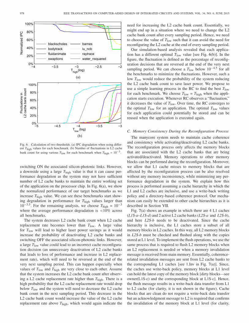
Fig. 6. Calculation of two thresholds. (a) IPC degradation when using differ-ent Thigh values for each benchmark. (b) Number of fluctuations in L2 cachebank count for using various Tlow for each benchmark when Thigh = 10−3.
switching ON the associated silicon-photonic links. However,a downside using a large Thigh value is that it can cause per-formance degradation as the system may not have sufficientnumber of L2 cache banks to maintain the entire working setof the application on the processor chip. In Fig. 6(a), we showthe normalized performance of our target benchmarks as weincrease Thigh value. We can see these benchmarks start show-ing degradation in performance for Thigh values larger than10−3.5. For the remaining analysis, we choose Thigh = 10−3
where the average performance degradation is <10% acrossall benchmarks.
The system decreases L2 cache bank count when L2 cachereplacement rate becomes lower than Tlow. A large valuefor Tlow will lead to higher laser power savings as it wouldincrease the probability of deactivating L2 cache banks andswitching OFF the associated silicon-photonic links. However,a large Tlow value could lead to an incorrect cache reconfigura-tion decision (an unnecessary deactivation of L2 cache banksthat leads to loss of performance and increase in L2 replace-ment rate), which will need to be reversed at the end of thevery next sampling period. This can happen especially whenvalues of Tlow and Thigh are very close to each other. Assumethat the system increases the L2 cache bank count after observ-ing a L2 cache replacement rate higher than Thigh. There is ahigh probability that the L2 cache replacement rate would dropbelow Tlow and the system will need to decrease the L2 cachebank count in the next sampling period. This decrease in theL2 cache bank count would increase the value of the L2 cachereplacement rate above Thigh, which would again indicate the
need for increasing the L2 cache bank count. Essentially, wemight end up in a situation where we need to change the L2cache bank count after every sampling period. Hence, we needto choose the value of Tlow such that it can avoid the need forreconfiguring the L2 cache at the end of every sampling period.
Our simulation-based analysis revealed that each applica-tion has a different optimal Tlow value [see Fig. 6(b)]. In thefigure, the fluctuation is defined as the percentage of reconfig-uration decisions that are reversed at the end of the very nextsampling period. We can choose a Tlow below 10−4.5 for allthe benchmarks to minimize the fluctuations. However, such alow Tlow would reduce the probability of the system reducingthe L2 cache bank count to save laser power. We propose touse a simple learning process in the RC to find the best Tlowfor each benchmark. We choose Tlow = Thigh when the appli-cation starts execution. Whenever RC observes a “fluctuation,”it decreases the value of Tlow. Over time, the RC converges tothe optimal Tlow for an application. The optimal Tlow valuesfor each application could potentially be stored and can bereused when the application is executed again.
C. Memory Consistency During the Reconfiguration Process
The manycore system needs to maintain cache coherenceand consistency while activating/deactivating L2 cache banks.The reconfiguration process only affects the memory blocksthat are associated with the L2 cache banks that are beingactivated/deactivated. Memory operations to other memoryblocks can be performed during the reconfiguration. Moreover,we allow that L1 cache misses to memory blocks that areaffected by the reconfiguration process can be also resolvedwithout any memory inconsistency, while minimizing any per-formance degradation in the system. We explain how thisprocess is performed assuming a cache hierarchy in which theL1 and L2 caches are inclusive, and use a write-back writingpolicy and a directory-based coherence protocol. Our mecha-nism can easily be extended to other cache hierarchies as it isdescribed in Section VII.
Fig. 7(a) shows an example in which there are 4 L1 caches(L1$-a–L1$-d) and 2 active L2 cache banks (L2$-a and L2$-b),and here L2$-b needs to be deactivated. Since the cachehierarchy is inclusive, the L1 caches store a subset of allmemory blocks in L2 caches. In this way, all L2 memory blocksin L2$-b must be checked and flushed along with the copiesstored at L1 level. To implement the flush operations, we use thesame process that is required to flush L2 memory blocks whenan L2 replacement is needed or when a memory invalidationmessage is received from main memory. Essentially, coherence-related invalidation messages are sent from L2 cache banks tothe corresponding L1 caches [see 1.Inv in Fig. 7(a)]. Since,the caches use write-back policy, memory blocks at L1 levelcan hold the latest copy of the memory block [dirty blocks—seeowner(L1$-c) and the corresponding block at L1$-c]. Hence,the flush message results in a write-back data transfer from L1to L2 cache (for clarity, it is not shown in the figure). Cacheblocks that are clean do not require a write-back data transferbut an acknowledgment message to L2 is required that confirmsthe invalidation of the memory block at L1 level (for clarity,

CHEN et al.: MANAGING LASER POWER IN SILICON-PHOTONIC NoC THROUGH CACHE AND NoC RECONFIGURATION 979
(a)
(b)
Fig. 7. Memory consistency in the reconfiguration process. (a) Deactivationof L2$-b. 1.Inv: message sent to all L1 caches that have a copy of the memoryblock to be flushed. 2.1–2.2 messages: L1 request using the old HB mappingfor a memory block that is NP. The old home L2 bank returns NACK indi-cating the petitions should go to L2 bank (L2$-a). 2.3–2.6 messages: theprevious L1 request is forwarded to the correct L2 bank that fetches the datafrom memory and sends it back to the L1 petitioner. 3.1–3.2 messages: L1petition for a memory block that has not been flushed yet by the old HB. Thisrequest can be processed as it has not been flushed. (b) Activation of L2$-b.1.Inv: message sent to the L1 cache that has a copy of the memory blockto be flushed. 2.1–2.6 messages: same steps as described for the deactivationprocess for a memory block that is NP in the old HB (L2$-a), and the L1petition is forwarded to the new L2 bank. 3.1–3.2 messages: same messageas those described for deactivation process.
it is not shown in the figure). It is worth noting that theseactions are exactly the same as when conventional invalidationmessages are employed. Hence, L1 cache controllers are notmodified to deal with our flush messages. Once a particularL2 memory block has been flushed from L1 caches (either awrite-back data transfer from the L1 with the dirty copy ofthe block, or a set of acknowledgments from each clean copyin L1 caches have been received at the L2 cache bank), theL2 cache bank will either transmit a write-back message tomemory [WB in Fig. 7(a)] in case of dirty blocks, or it willsimply remove the associated L2 cache bank entry in case ofa clean block. Then, the coherence status of these L2 cacheentries change to not-present (NP).
To avoid performance loss during the flushing of memoryblocks from the L2 banks that are being deactivated during thereconfiguration process, we allow their corresponding L2 bankcontrollers to continue processing L1 petitions as follows: allL1 petitions that go to memory blocks that are stored in the L2bank (they are not in NP state) are processed using the MESIprotocol [see 3.1 Req and 3.2 Data in Fig. 7(a)]. However, L1petitions to memory blocks that are not cached in the L2 bankbecause either they have been flushed during the reconfigura-tion process, or they have never been referenced, or they havebeen recently replaced (they are in NP state—see 2.1 Req)are not forwarded toward main memory to get the requestedmemory block. In this case, and only during the reconfigura-tion process, the L2 bank controller returns a NACK messagefor each of these L1 petitions [2.2 NACK in Fig. 7(a) for thecase where L2$-b is being deactivated]. The NACK messagecontains the number of bits that should be used by the L1controller to determine the HB field from the memory blockaddress (see Fig. 5). In that way, the L1 controllers know thenew L2 bank that will be responsible for these L1 petitionsand send petitions to it (see messages from 2.3 to 2.6). Inshort, all L1 petitions are served during the reconfigurationprocess. Note that, our proposal requires minimal modifica-tions to the L2 cache controller to deal with the NP stateduring the reconfiguration process.
Fig. 7(b) shows the L2 cache bank activation process. Inthis example, there are four L1 caches (L1$-a–L1$-d) and oneactive L2 cache bank (L2$-a), and L2$-b bank needs to be acti-vated. Note that, as we mentioned in Section V-A, the first stepof the reconfiguration process is that the RC sends the new sizeof the HB field to the current set of L2 banks. Second, the RCstarts the activation of the new L2 banks and the correspond-ing laser sources and silicon-photonic links. Once the new setof L2 banks along with the associated silicon-photonic linksare powered up the RC begins the new mapping of memoryblocks to the new L2 bank configuration.
To apply the new mapping of memory blocks to the L2banks, we need to first identify the L2 cache banks that arecurrently active and are serving the L1 cache requests (prior toreconfiguration) that would be served by L2$-b after reconfig-uration. We then need to flush these relevant memory blocksfrom these L2 cache banks back to memory. To accomplishthat, the current L2 cache banks use the new size of the HBfield (which they know by this stage). They compare the newHB field against their cached memory blocks’ tag field, anddetermine which cached blocks to flush. The process of flush-ing L2 memory blocks would be similar to that explained inthe L2 cache bank deactivation process [1. Inv, WB and Ackin Fig. 7(a)].
To minimize performance degradation, we allow the appli-cation execution to continue during the reconfiguration processwhile maintaining memory consistency. First, all L1 requeststhat go to memory blocks that are not affected by the recon-figuration process (cached blocks with correct HB bits) can beprocessed as in the MESI protocol [2.1 and 2.2 in Fig. 7(b)].Second, the remaining set of L1 petitions that correspondto the memory blocks who will belong to the newly acti-vated L2 banks will go first to the current home L2 bank

980 IEEE TRANSACTIONS ON COMPUTER-AIDED DESIGN OF INTEGRATED CIRCUITS AND SYSTEMS, VOL. 34, NO. 6, JUNE 2015
(the L1 petitioners do not know the new size for the HBfield). These L2 banks send NACK messages that contain thesize of the new HB field to the L1 petitioners [2.2 NACK inFig. 7(b)]. To keep memory consistency, the NACK messagewill only be sent from the old L2 banks to the L1 petitionersafter the requested memory block has been completely flushedfrom the old L2 bank (it gets an NP state in the old L2 bank).In this way, our mechanism avoids stopping the system duringthe reconfiguration process [see messages from 2.3 to 2.6 inFig. 7(b)] and guarantees that there will be a unique copy ofthe memory block cached at L2 level, thereby avoiding thememory inconsistency.
Note that the RC does not need to communicate the recon-figuration decision to L1 caches, as the active L2 banks willsend this information to the L1 caches through the NACKmessages explained above. For instance, if an L1 cache doesnot know the new set of L2 active banks, and sends it petitionsto an incorrect L2 bank, the L2 bank will return the NACKmessage that stores the number of bits required to identify thecorrect mapping of memory blocks to L2 banks (the new HBfield). Moreover, if the L1 cache controller tries to send a mes-sage to a previously deactivated L2 bank, it will not be ableto establish the communication with this L2 bank because thecorresponding silicon-photonic channel is deactivated. So, theL1 cache controller will then update the size of the HB fieldby removing one bit to the HB field (e.g., from 3 bits thatidentifies 8 L2 banks to 2 bits that refers to 4 L2 banks) andtry to send a message to an L2 bank based on the new map-ping. The L1 cache controller will repeat the previous processuntil it gets an active silicon-photonic channel (correspondingto an active L2 bank). If after sending the L1 petition, thisL1 petition reaches an incorrect L2 bank, that L2 bank willreturn a NACK message (containing the number of bits to beused for determining the new mapping) to the L1 petitioner sothat the L1 petition will then send the petition to the correctL2 bank. The modifications to both the L1 and L2 cache con-trollers to deal with this new scenario (not implemented in aregular MESI protocol) results in minimal overhead comparedto the larger laser power savings.
VI. EVALUATION
In this section, we quantify the power savings obtained byusing our proposed cache and NoC reconfiguration technique.
A. Simulation Methodology
We use the Gem5 full-system simulator [10] to evaluate ourproposed idea of using L2 cache and NoC reconfiguration forlaser power savings on the 64-core target system describedin Section III. We enable the Ruby memory system for anaccurate modeling of the shared multibank L2 cache hierar-chy. We run PARSEC [11] and SPLASH-2 [12] benchmarksin their parallel regions with the large input set, and check forthe need for L2 cache reconfiguration after every ten millioninstructions (committed by all 64 cores), which is approxi-mately 500 μs for our target system. Each benchmark executesa total of four billion instructions resulting in 400 reconfigura-tion sampling periods. After every sampling period, we check
the replacement rate using performance counters to analyzethe need for L2 cache reconfiguration.
We use McPAT [38] and Cacti 5.3 [39] to calculate thecore power and cache power, respectively. The McPAT outputis calibrated using the Intel SCC [1] published power valuesand is then scaled to 22 nm technology [40]. We use the pho-tonic technology described in Section IV to calculate laserpower, Tx/Rx power and thermal tuning power in the NoC.We calculate EDP [total system power * (application execu-tion cycles/system frequency)2] of the entire system to evaluatethe overall impact of our proposed technique on the balanceof system performance and power.
B. Reconfiguration Opportunities
Fig. 8(a) and (b) shows the IPC trace and L2 cachereplacement rate trace, respectively, for a 64-core systemwith different number of L2 cache banks when run-ning blackscholes, bodytrack, fluidanimate,swaptions, barnes, lu_ncb, raytrace, andwater_nsquared benchmarks. The replacement ratecan be used as a metric for a fairly accurate prediction ofwhether we need to increase or decrease the number of L2cache banks. A high L2 cache replacement rate generallyindicates the need for a larger cache capacity, while a lowL2 cache replacement rate indicates that cache capacity islarger than what is required. Fig. 8(c) compares the traceof the ideal L2 cache bank count determined using offlineanalysis and the trace of the L2 cache bank count chosen bythe RC at runtime. The offline analysis chooses the minimalL2 cache bank count required to maximize performance aftereach sampling period. RC determines the L2 cache bankcount based on the L2 cache replacement rate during thesampling period and compares it with two thresholds Thighand Tlow to determine the L2 cache bank count for the nextperiod. Fig. 8(c) shows that the optimal L2 cache bank countvaries both across applications and within applications overtime and the L2 cache bank count chosen by the RC closelymatches with the L2 cache bank count chosen by the offlineanalysis. Our proposed reconfiguration policy ensures thatthe L2 cache bank count tracks the changes in L2 cachereplacement rate, and therefore harnesses any opportunity ofsaving laser power by reducing the L2 cache bank count.The optimal L2 cache bank count for blackscholes islower than that for barnes. This indicates more savings inlaser power when running blackscholes. In case of thebarnes application, the optimal L2 cache bank count variesas the application goes through different execution phases,thus providing various levels of laser power savings.
C. Reconfiguration Benefits
Fig. 9 shows the impact of reconfiguration on systemperformance and power dissipation (using conservative silicon-photonic link design). Here, we compare the performanceand power dissipation of a 64-core system that uses a fixednumber of 1, 2, 4, and 8 banks with a 64-core system thatuses our proposed cache and NoC reconfiguration policy. Wedid not consider cases with 3, 5, 6, and 7 active L2 cache

CHEN et al.: MANAGING LASER POWER IN SILICON-PHOTONIC NoC THROUGH CACHE AND NoC RECONFIGURATION 981
Fig. 8. IPC, L2 replacement rate, and L2 cache bank count tracing for selected benchmarks. (a) IPC of each benchmark with a fixed L2 cache bank count:1, 2, 4, and 8 banks. (b) Measured L2 replacement rate with a fixed L2 cache bank count. (c) Optimal L2 cache bank count determined offline and the L2cache bank count chosen by the RC at runtime.
banks as the mapping of the cache address becomes compli-cated for these bank counts and the overhead of L2 cachereconfiguration process increases. For this comparison, weassume the waveguide loss is 3 dB/cm. By deactivating redun-dant L2 cache banks and their associated silicon-photoniclinks, on average the runtime reconfiguration saves laserpower by 23.8% (peak value 74.3%), cache power by 22.7%(peak value 72.9%), and system power by 9.9% (peak value
30.6%), compared to the case where all 8 L2 cache banksare ON all the time while having an average IPC degrada-tion of 0.65% (peak value 2.6%). It should be noted that forthe fluidanimate, swaptions, barnes, lu_ncb,and raytrace benchmarks, the laser power when usingreconfiguration is comparable to the case when using all eightbanks because these benchmarks require all eight banks to beactive to maximize performance (seen from Fig. 8).

982 IEEE TRANSACTIONS ON COMPUTER-AIDED DESIGN OF INTEGRATED CIRCUITS AND SYSTEMS, VOL. 34, NO. 6, JUNE 2015
Fig. 9. Impact of runtime reconfiguration on system performance and power. We compare a system with runtime reconfiguration to systems with fixed numberof L2 cache banks. Here, “1,” “2,” “4,” and “8” represents the simulations with fixed 1, 2, 4, and 8 banks, respectively and “R” represents the simulationswith runtime reconfigurable L2 cache bank count. We show the power breakdown and IPC of 8 benchmarks and their geometric means.
Fig. 10. Impact of waveguide loss on the system EDP improvement (averagedacross all benchmarks). The waveguide loss varies in a range of 1–3 dB/cm,while fixing the losses in the remaining optical device losses to the valuesshown in Table II.
Fig. 10 shows EDP improvement after applying the runtimereconfiguration. The baseline used for comparison is a systemwith all eight L2 cache banks active all the time. The waveg-uide loss in the future silicon-photonic links is projected tobe in a range of 1–3 dB/cm and is expected to be the dom-inant loss component. Here, the ring through loss is fixed at1e-2 dB/ring. If we assume a conservative waveguide loss of3 dB/cm, the runtime reconfiguration reduces entire systempower dissipation by 9.9% (peak value 30.6%) and improvesthe entire system EDP by 9.2% on average (peak value 26.9%).If we assume a more aggressive waveguide loss of 1 dB/cm,the reconfiguration saves system power by 5.2% (peak value16.0%) and improves system EDP by 4.3% on average (peakvalue 13.2%).
Similarly, Fig. 11 shows EDP improvement versus the ringthrough loss. The through loss in the future silicon-photoniclinks is projected in a range of 1e-5–1e-2 dB/ring. Here, thewaveguide loss is fixed at 3 dB/cm. If we assume a conserva-tive ring through loss of 1e-2 dB/ring, the runtime reconfigu-ration reduces entire system power dissipation by 9.9% (peakvalue 30.6%) and improves the entire system EDP by 9.2% onaverage (peak value 26.9%). If we assume a more aggressivering through loss of 1e-5 dB/ring, the reconfiguration saves
Fig. 11. Impact of ring through loss on the system EDP improvement(averaged across all benchmarks). The ring through loss varies in a rangeof 1e-5–1e-2 dB/ring, while fixing the losses in the remaining optical devicelosses to the values shown in Table II.
system power by 8.6% (peak value 26.4%) and improves sys-tem EDP by 7.8% on average (peak value 23%). The reductionof ring through loss has a smaller impact on the system EDPimprovement than the reduction of waveguide loss because thering through loss contributes a smaller amount of losses amongall the optical loss components along the silicon-photonicwaveguide.
Fig. 12 shows the overhead of the reconfiguration process.The reconfiguration process of L2 cache banks requires sev-eral cycles for flushing memory blocks from L2 cache banksand L1 cache (through L2) to the main memory, and fetchingthese memory blocks back to the appropriate active L2 cachebanks. We measured the average reconfiguration overhead foreach benchmark. In the worst case (when half the L2 cacheblocks are flushed), a maximum of 18 000 cycles are spentin a reconfiguration that accounts for less than 1.782% of theexecution time of one sampling interval (in the worst case).Our simulations also show that a maximum of ten reconfigu-rations were required over the 400 sampling intervals. Thetotal time spent in reconfiguration is less than 0.045% ofthe entire execution time of a benchmark. Correspondingly,the energy overhead of the RC is minimal and gets amor-tized across the entire execution time of the benchmark. The

CHEN et al.: MANAGING LASER POWER IN SILICON-PHOTONIC NoC THROUGH CACHE AND NoC RECONFIGURATION 983
Fig. 12. Average overhead (in terms of number of cycles) per recon-figuration for various benchmarks. The overhead includes the clock cyclesspent in flushing memory blocks during reconfiguration, notifying updatedconfiguration.
average execution time of a benchmark is 12 ms, and after eachreconfiguration we had an average of 2893 additional DRAMaccesses for flushing and refetching 512-bit cache blocks.As a DRAM access costs less than 10 pJ/bit [41], a maxi-mum of ten reconfigurations for each benchmark costs about150 μJ (10 reconfiguration × 2893 access/reconfiguration ×512 bit/access × 10 pJ/bit), over the 12 ms execution time.It should be noted that a benchmark does not stop executionwhile the system is being reconfigured. It continues to exe-cute using the older L2 configuration. It switches to the newL2 configuration once the L2 cache banks and the associatedsilicon-photonic links are activated/deactivated. The RC can beimplemented as a combinational logic and requires a single-bitwire for communicating to/from L2 cache banks. Comparedto the overall chip area, the area of the RC is minimal.
VII. APPLICATION OF RECONFIGURATION POLICY TO
ALTERNATE MANYCORE ARCHITECTURES
The proposed methodology for managing laser powerthrough cache reconfiguration was specifically designedassuming an inclusive cache hierarchy with two levels ofwrite-back caches (a private L1 caches and a logically-sharedphysically-distributed L2 cache), and a sophisticated imple-mentation of a silicon-photonic crossbar. In this section, wediscuss how our proposal would operate with other configu-rations of the cache hierarchy, alternate silicon-photonic NoCarchitectures, and large core counts.
A. Alternate Cache Configurations
Our reconfiguration system changes on-chip cache capac-ity based on application demand at runtime. In general, thisprocess can be applied to any cache hierarchy or cache coher-ence protocol, as long as every reconfiguration step leavesthe memory system in a consistent state. Here, we discuss theapplication of our cache reconfiguration policy to an exclusivecache hierarchy and a write-through writing policy.
An inclusive hierarchy is commonly present in almost allcurrent processor architectures as it eases the implementationof coherency protocols. However, a cache design that enforcesinclusion is inherently wasteful of cache space and networkbandwidth. The reason for this is that every cache line in lower
levels is duplicated in the higher levels, and updates in lowerlevels trigger many more updates in higher levels, wasting net-work bandwidth. This negative effect on our reconfigurationprocess is discussed in Section V-C, where the deactivation ofa L2 cache bank requires parsing through all its bank entriesto invalidate or flush all L1 cache entries that are copies ofthe entries in the L2 cache to be deactivated, hence wast-ing network bandwidth and energy. If we relax the inclusivityproperty and consider a mutual exclusive hierarchy, the cacheimplementation would be more complex from memory hier-archy standpoint (cores can communicate directly to the L2cache banks, and block swapping between the two levels ofcaches must be made to guarantee exclusivity), but our recon-figuration process would be simpler and more efficient. Since,the memory blocks of the chosen L2 cache bank are NP inother L1 caches, we can deactivate the L2 cache bank with-out the need for flushing blocks from L1 caches, hence savingnetwork bandwidth. During the process of deactivation, allrequests of block swapping and requests from cores to thatL2 cache bank would have to be denied using NACK mes-sages. Similar to an inclusive hierarchy, the process to activatea new L2 cache bank would imply checking entries in L2cache banks, and flushing all the entries that will belong tothe new L2 cache bank back to memory.
Another important consideration is the writing policy imple-mented in caches. It is clear that the use of a write-backpolicy is efficient from the performance and network band-width perspectives, because when a processor core writes amemory block, it is simply marked as “dirty” and futureaccesses to it do not result in a cache miss. Upon a replace-ment or coherency-related invalidation, that block is evictedand its content is written back to a higher level of cache ormemory. Due to the efficiency of this policy, our reconfig-uration system has been designed with this kind of policy.Nonetheless, if we decide to use a write-through policy forL1 caches and L2 cache banks, the design of our reconfigura-tion process would be more efficient. The reason is that sincemain memory always holds the most recent value written toevery memory block, deactivating an L2 cache bank can beperformed without the need for flushing any data from L1caches. However, in an inclusive hierarchy with write-throughcaches, future references to blocks in L1 caches belongingto the deactivated L2 cache could still have a hit, violatingthe inclusivity property. Therefore, the reconfiguration processwould also need to invalidate such L1s’ blocks consumingextra network bandwidth.
B. Alternate NoC Architectures and Large Core Counts
For evaluation of our reconfiguration policy, we consid-ered a 64-core target system consisting of a silicon-photoniccrossbar topology. However, our reconfiguration policy canbe easily extended to other NoC topologies. The scope ofapplication of our reconfiguration policy is really only lim-ited by the physical implementation of the NoC. If the NoCemployed to interconnect the L1 caches and L2 cache banksuses dedicated point-to-point silicon links, then the deactiva-tion of a L2 cache bank can enable the deactivation of the

984 IEEE TRANSACTIONS ON COMPUTER-AIDED DESIGN OF INTEGRATED CIRCUITS AND SYSTEMS, VOL. 34, NO. 6, JUNE 2015
corresponding point-to-point silicon-photonic links. However,if the NoC is designed using shared silicon-photonic links,these links cannot be deactivated until all components attachedto them have been also deactivated. Given that a logicaltopology can be mapped to any physical topology (sub-ject to power/performance constraints) [42], in principle ourreconfiguration policy can be applied to any logical topology.
Future manycore systems are expected to have thousandsof cores on a chip. These thousand-core systems will stillhave the conventional L1–L2 cache hierarchy and are expectedto support data-center style multiprogrammed workloads. Thevariations in the L2 cache size requirements across the dif-ferent applications presents an opportunity to apply our cachereconfiguration policy. In addition, these thousand-core sys-tems are expected to use the idea of “dark silicon,” whereonly a fraction of the cores are active at a given point of timeto manage power dissipation and to slow down aging. Thisapproach of selectively using cores, and hence selectively acti-vating L1/L2 caches also provides an opportunity to apply ourproposed policy to reduce laser power.
VIII. CONCLUSION
The large laser power dissipated in the silicon-photonic NoCis limiting its widespread adoption in the design of manycoresystems. We propose a runtime cache and NoC reconfigurationpolicy, where we activate/deactivate L2 cache banks depend-ing on the spatial and temporal variations in the applicationbehavior, and then switch ON/OFF the silicon-photonic linksassociated with these L2 cache banks to dynamically managethe laser power. The key idea is that for a given applica-tion at any given point of time, we operate the manycoresystem using the minimum number of L2 cache banks andsilicon-photonic links required to achieve maximum applica-tion performance. Our policy is scalable to large core countsand is applicable to alternate cache and NoC architectures. Ona 64-core target system with a silicon-photonic crossbar NoC,on average our proposed technique reduces laser power andsystem power by 23.8% (peak value 74.3%) and 9.9% (peakvalue 30.6%), respectively, and improves EDP by 9.2% (peakvalue 26.9%). Our proposed laser management methodologycan potentially expedite the process of widespread adoptionof silicon-photonic link technology in manycore processors.
ACKNOWLEDGMENT
The authors would like to thank J. Klamkin and M. Popovicfor helpful discussions on photonic device designs.
REFERENCES
[1] J. Howard et al., “A 48-core IA-32 message-passing processor withDVFS in 45nm CMOS,” in Proc. IEEE Int. Solid-State CircuitsConf. Dig. Tech. Papers (ISSCC), San Francisco, CA, USA, 2010,pp. 108–109.
[2] S. Bell et al., “Tile64-processor: A 64-core SoC with mesh interconnect,”in Proc. IEEE Int. Solid-State Circuits Conf. Dig. Tech. Papers (ISSCC),San Francisco, CA, USA, 2008, pp. 88–598.
[3] S. Vangal et al., “An 80-tile sub-100-W teraFLOPS processor in 65-nm CMOS,” IEEE J. Solid-State Circuits, vol. 43, no. 1, pp. 29–41,Jan. 2008.
[4] A. Joshi et al., “Silicon-photonic clos networks for global on-chip com-munication,” in Proc. 3rd ACM/IEEE Int. Symp. Netw. Chip (NoCS),San Diego, CA, USA, 2009, pp. 124–133.
[5] D. Vantrease et al., “Corona: System implications of emerging nanopho-tonic technology,” in Proc. 35th Int. Symp. Comput. Archit. (ISCA),Beijing, China, 2008, pp. 153–164.
[6] Y. Pan et al., “Firefly: Illuminating future network-on-chip withnanophotonics,” in Proc. 36th Annu. Int. Symp. Comput. Archit. (ISCA),Austin, TX, USA, 2009, pp. 429–440.
[7] M. J. Cianchetti, J. C. Kerekes, and D. H. Albonesi, “Phastlane: A rapidtransit optical routing network,” in Proc. 36th Annu. Int. Symp. Comput.Archit. (ISCA), Austin, TX, USA, 2009, pp. 441–450.
[8] H. Wassel et al., “Opportunities and challenges of using plasmoniccomponents in nanophotonic architectures,” IEEE J. Emerg. Sel. TopicsCircuits Syst., vol. 2, no. 2, pp. 154–168, Jun. 2012.
[9] Y. Pan, J. Kim, and G. Memik, “Featherweight: Low-cost optical arbi-tration with QoS support,” in Proc. 44th Annu. IEEE/ACM Int. Symp.Microarchit. (MICRO), Porto Alegre, Brazil, 2011, pp. 105–116.
[10] N. Binkert et al., “The M5 Simulator: Modeling networked systems,”IEEE Micro, vol. 26, no. 4, pp. 52–60, Jul./Aug. 2006.
[11] C. Bienia, S. Kumar, J. P. Singh, and K. Li, “The PARSEC bench-mark suite: Characterization and architectural implications,” in Proc.17th Int. Conf. Parallel Archit. Compil. Tech. (PACT), Toronto, ON,Canada, 2008, pp. 72–81.
[12] S. Woo, M. Ohara, E. Torrie, J. Singh, and A. Gupta, “The SPLASH-2programs: Characterization and methodological considerations,” in Proc.22nd Annu. Int. Symp. Comput. Archit., Liguria, Italy, 1995, pp. 24–36.
[13] A. Shacham, K. Bergman, and L. P. Carloni, “On the design of a pho-tonic network-on-chip,” in Proc. 1st Int. Symp. Netw. Chip (NOCS),Washington, DC, USA, 2007, pp. 53–64.
[14] H. Gu, J. Xu, and W. Zhang, “A low-power fat tree-based opticalnetwork-on-chip for multiprocessor system-on-chip,” in Proc. DesignAutom. Test Europe Conf. Exhibit. (DATE), Nice, France, 2009, pp. 3–8.
[15] N. Kirman et al., “Leveraging optical technology in future bus-basedchip multiprocessors,” in Proc. 39th Annu. IEEE/ACM Int. Symp.Microarchit. (MICRO), Orlando, FL, USA, 2006, pp. 492–503.
[16] Y. Pan, J. Kim, and G. Memik, “FlexiShare: Channel sharing foran energy-efficient nanophotonic crossbar,” in Proc. IEEE 16th Int.Symp. High Perform. Comput. Archit. (HPCA), Bangalore, India, 2010,pp. 1–12.
[17] L. Zhou and A. Kodi, “PROBE: Prediction-based optical bandwidth scal-ing for energy-efficient NoCs,” in Proc. 7th IEEE/ACM Int. Symp. Netw.Chip (NoCS), Tempe, AZ, USA, 2013, pp. 1–8.
[18] C. Li, M. Browning, P. V. Gratz, and S. Palermo, “LumiNOC: Apower-efficient, high-performance, photonic network-on-chip for futureparallel architectures,” in Proc. 21st Int. Conf. Parallel Archit. Compil.Tech. (PACT), Minneapolis, MN, USA, 2012, pp. 421–422.
[19] C. Chen and A. Joshi, “Runtime management of laser power in silicon-photonic multibus NoC architecture,” IEEE J. Sel. Topics QuantumElectron., vol. 19, no. 2, Mar. 2013, Art. ID 3700713.
[20] J. Sim, J. Lee, M. Qureshi, and H. Kim, “FLEXclusion: Balancing cachecapacity and on-chip bandwidth via flexible exclusion,” in Proc. 39thAnnu. Int. Symp. Comput. Archit. (ISCA), Washington, DC, USA, 2012,pp. 321–332.
[21] C.-J. Wu et al., “SHiP: Signature-based hit predictor for high perfor-mance caching,” in Proc. 44th Annu. IEEE/ACM Int. Symp. Microarchit.,Porto Alegre, Brazil, 2011, pp. 430–441.
[22] C. Chen et al., “Sharing and placement of on-chip laser sourcesin silicon-photonic NoCs,” in Proc. 8th ACM/IEEE Int. Symp. Netw.Chip (NoCS), Ferrara, Italy, 2014, pp. 1–8.
[23] S. Beamer et al., “Re-architecting DRAM memory systems with mono-lithically integrated silicon photonics,” in Proc. 37th Annu. Int. Symp.Comput. Archit. (ISCA), Saint-Malo, France, 2010, pp. 129–140.
[24] J. S. Orcutt et al., “Open foundry platform for high-performanceelectronic-photonic integration,” Opt. Exp., vol. 20, no. 11,pp. 12222–12232, May 2012.
[25] M. Georgas et al., “A monolithically-integrated optical transmitter andreceiver in a zero-change 45nm SOI process,” in Proc. Symp. VLSICircuits Dig. Tech. Papers, Honolulu, HI, USA, 2014, pp. 1–2.
[26] Y. Liu, J. M. Shainline, X. Zeng, and M. A. Popovic, “Ultra-low-loss CMOS-compatible waveguide crossing arrays based on multimodeBloch waves and imaginary coupling,” Opt. Lett., vol. 39, no. 2,pp. 335–338, Jan. 2014.
[27] X. Zheng et al., “2-pj/bit (on-chip) 10-Gb/s digital CMOS silicon pho-tonic link,” IEEE Photon. Technol. Lett., vol. 24, no. 14, pp. 1260–1262,Jul. 15, 2012.

CHEN et al.: MANAGING LASER POWER IN SILICON-PHOTONIC NoC THROUGH CACHE AND NoC RECONFIGURATION 985
[28] R. E. Camacho-Aguilera et al., “An electrically pumped germaniumlaser,” Opt. Exp., vol. 20, no. 10, pp. 11316–11320, May 2012.
[29] L. Liu et al., “A thermally tunable III-V compound semiconductormicrodisk laser integrated on silicon-on-insulator circuits,” IEEE Photon.Technol. Lett., vol. 22, no. 17, pp. 1270–1272, Sep. 1, 2010.
[30] T. Wang, H. Liu, A. Lee, F. Pozzi, and A. Seeds, “1.3-μm InAs/GaAsquantum-dot lasers monolithically grown on Si substrates,” Opt. Exp.,vol. 19, no. 12, pp. 11381–11386, Jun. 2011.
[31] K. Lawniczuk et al., “8-channel AWG-based multiwavelength laser fab-ricated in a multi-project wafer run,” in Proc. 23rd Int. Conf. IndiumPhosphide Related Mater. Compound Semiconduct. Week (CSW/IPRM),Berlin, Germany, 2011, pp. 1–4.
[32] D. Livshits et al., “Cost-effective WDM optical interconnects enabledby quantum dot comb lasers,” Proc. SPIE, vol. 7607, Feb. 2010,Art. ID 76070W.
[33] L. A. Coldren, S. W. Corzine, and M. L. Mashanovitch, “Micronwaveand optical engineering,” in Diode Laser and Photonic IntegratedCircuits, 2nd ed. Hoboken, NJ, USA: Wiley, 2012.
[34] J. Klamkin et al., “Directly modulated narrowband slab-coupled opticalwaveguide laser,” Electron. Lett., vol. 46, no. 7, pp. 522–523, 2010.
[35] G. Sarlet, G. Morthier, and R. Baets, “Wavelength and mode stabiliza-tion of widely tunable SG-DBR and SSG-DBR lasers,” IEEE Photon.Technol. Lett., vol. 11, no. 11, pp. 1351–1353, Nov. 1999.
[36] S. Musalappa, “An energy efficient data cache implementing 2-way LRCarchitecture,” M.S. thesis, Dept. Elect. Comput. Eng., Mississippi StateUniv., Starkville, MS, USA, 2006.
[37] M. K. Qureshi, A. Jaleel, Y. N. Patt, S. C. Steely, and J. Emer,“Adaptive insertion policies for high performance caching,” in Proc.34th Annu. Int. Symp. Comput. Archit. (ISCA), San Diego, CA, USA,2007, pp. 381–391.
[38] S. Li et al., “McPAT: An integrated power, area, and timing modelingframework for multicore and manycore architectures,” in Proc. 42ndAnnu. IEEE/ACM Int. Symp. Microarchit. (MICRO), New York, NY,USA, 2009, pp. 469–480.
[39] S. Thoziyoor, N. Muralimanohar, J.-H. Ahn, and N. P. Jouppi, “CACTI5.1,” HP Labs, Hewlett-Packard Develop. Company, Palo Alto, CA,USA, Tech. Rep. HPL-2008-20, 2008.
[40] J. Meng, C. Chen, A. K. Coskun, and A. Joshi, “Run-time energy man-agement of manycore systems through reconfigurable interconnects,” inProc. 21st Great Lakes Symp. VLSI (GLSVLSI), Lausanne, Swizerland,2011, pp. 43–48.
[41] T. Vogelsang, “Understanding the energy consumption of dynamic ran-dom access memories,” in Proc. 43rd Annu. IEEE/ACM Int. Symp.Microarchit. (MICRO), Atlanta, GA, USA, 2010, pp. 363–374.
[42] C. Batten, A. Joshi, V. Stojanovc, and K. Asanovic, “Designing chip-level nanophotonic interconnection networks,” in Integrated OpticalInterconnect Architectures for Embedded Systems. New York, NY, USA:Springer, 2013, pp. 81–135.
Chao Chen (S’10–M’14) received the B.Eng.degree in electronic engineering from Shanghai JiaoTong University, Shanghai, China, in 2005, the M.S.degree in electronic and electrical engineering fromthe Pohang University of Science and Engineering,Pohang, Korea, in 2007, and the Ph.D. degreein computer engineering from Boston University,Boston, MA, USA, in 2014.
He is currently a Performance-Modeling Engineerwith the Digital Networking Group, FreescaleSemiconductor Inc., Austin, TX, USA. His current
research interests include performance modeling, system and network-on-chiparchitecture, and silicon-photonic technology.
José L. Abellán (S’07–M’08) received the B.S.,M.S., and Ph.D. degrees in computer science andengineering from the University of Murcia, Murcia,Spain, in 2007, 2008, and 2012, respectively.
From 2012 to 2014, he was a Post-DoctoralResearcher at Boston University, Boston, MA,USA, under the supervision of Prof. A. Joshi.He is currently an Assistant Professor with theComputer Science Department, Catholic Universityof Murcia, Murcia. His current research interestsinclude general-purpose computing on graphics pro-
cessing units architecture, multicore/manycore architectures, networks-on-chip, high performance and green computing, parallel programming, CMOS,and nanophotonic technologies.
Ajay Joshi (S’99–M’07) received the B.Eng.degree in computer engineering from the Universityof Mumbai, Mumbai, India, in 2001, and theM.S. and Ph.D. degrees in electrical and com-puter engineering from the Georgia Institute ofTechnology, Atlanta, GA, USA, in 2003 and 2006,respectively.
From 2006 to 2009, he was a Post-DoctoralResearcher at the Massachusetts Institute ofTechnology, Cambridge, MA, USA. He is cur-rently an Assistant Professor with the Electrical and
Computer Engineering Department, Boston University, Boston, MA, USA. Hiscurrent research interests include very large scale integration design includ-ing circuits and systems for communication and computation and emergingdevice technologies including silicon photonics and memristors.
Prof. Joshi was the recipient of the National Science Foundation CAREERAward in 2012.
Related Documents