8XC196K x, 8XC196J x, 87C196CA Microcontroller Family User’s Manual Includes 8XC196KQ, 8XC196KR, 8XC196KS, 8XC196KT, 8XC196JQ, 8XC196JR, 8XC196JT, 8XC196JV, 87C196CA

Welcome message from author
This document is posted to help you gain knowledge. Please leave a comment to let me know what you think about it! Share it to your friends and learn new things together.
Transcript
8XC196Kx, 8XC196Jx, 87C196CA Microcontroller Family User’s Manual
Includes 8XC196KQ, 8XC196KR, 8XC196KS, 8XC196KT, 8XC196JQ, 8XC196JR, 8XC196JT, 8XC196JV, 87C196CA

8XC196Kx,8XC196Jx, 87C196CA
Microcontroller FamilyUser’s Manual
Includes8XC196KQ, 8XC196KR, 8XC196KS, 8XC196KT,
8XC196JQ, 8XC196JR, 8XC196JT, 8XC196JV,87C196CA
June 1995 Order Number 272258-002

ii
Information in this document is provided solely to enable use of Intel products. Intel assumes no liability whatsoever, includinginfringement of any patent or copyright, for sale and use of Intel products except as provided in Intel’s Terms and Conditionsof Sale for such products.
Intel Corporation makes no warranty for the use of its products and assumes no responsibility for any errors which may appearin this document nor does it make a commitment to update the information contained herein.
Intel retains the right to make changes to these specifications at any time, without notice.
Contact your local Intel sales office or your distributor to obtain the latest specifications before placing your product order.
MDS is an ordering code only and is not used as a product name or trademark of Intel Corporation.
Intel Corporation and Intel's FASTPATH are not affiliated with Kinetics, a division of Excelan, Inc. or its FASTPATH trademarkor products.
*Other brands and names are the property of their respective owners.
Additional copies of this document or other Intel literature may be obtained from:
Intel CorporationLiterature SalesP.O. Box 7641Mt. Prospect, IL 60056-7641
or call 1-800-879-4683
© INTEL CORPORATION, 1996

iii
CONTENTS
CHAPTER 1GUIDE TO THIS MANUAL
1.1 MANUAL CONTENTS ................................................................................................... 1-1
1.2 NOTATIONAL CONVENTIONS AND TERMINOLOGY ................................................ 1-3
1.3 RELATED DOCUMENTS .............................................................................................. 1-5
1.4 ELECTRONIC SUPPORT SYSTEMS ........................................................................... 1-81.4.1 FaxBack Service .......................................................................................................1-81.4.2 Bulletin Board System (BBS) ....................................................................................1-9
1.4.2.1 How to Find MCS® 96 Microcontroller Files on the BBS ......................................1-91.4.2.2 How to Find ApBUILDER Software and Hypertext Documents on the BBS ......1-10
1.4.3 CompuServe Forums ..............................................................................................1-101.4.4 World Wide Web .....................................................................................................1-10
1.5 TECHNICAL SUPPORT .............................................................................................. 1-11
1.6 PRODUCT LITERATURE............................................................................................ 1-11
1.7 TRAINING CLASSES .................................................................................................. 1-11
CHAPTER 2ARCHITECTURAL OVERVIEW
2.1 TYPICAL APPLICATIONS............................................................................................. 2-1
2.2 DEVICE FEATURES ..................................................................................................... 2-2
2.3 BLOCK DIAGRAM......................................................................................................... 2-22.3.1 CPU Control ..............................................................................................................2-42.3.2 Register File ..............................................................................................................2-42.3.3 Register Arithmetic-logic Unit (RALU) .......................................................................2-4
2.3.3.1 Code Execution ....................................................................................................2-52.3.3.2 Instruction Format ................................................................................................2-5
2.3.4 Memory Controller ....................................................................................................2-62.3.5 Interrupt Service ........................................................................................................2-6
2.4 INTERNAL TIMING........................................................................................................ 2-7
2.5 INTERNAL PERIPHERALS........................................................................................... 2-82.5.1 I/O Ports ....................................................................................................................2-92.5.2 Serial I/O (SIO) Port ..................................................................................................2-92.5.3 Synchronous Serial I/O (SSIO) Port ..........................................................................2-92.5.4 Slave Port (8XC196Kx Only) ..................................................................................2-102.5.5 Event Processor Array (EPA) and Timer/Counters .................................................2-102.5.6 Analog-to-digital Converter .....................................................................................2-112.5.7 Watchdog Timer ......................................................................................................2-112.5.8 CAN Serial Communications Controller (87C196CA Only) .....................................2-11
2.6 SPECIAL OPERATING MODES ................................................................................. 2-112.6.1 Reducing Power Consumption ...............................................................................2-12

CONTENTS
iv
2.6.2 Testing the Printed Circuit Board ............................................................................2-122.6.3 Programming the Nonvolatile Memory ....................................................................2-12
2.7 DESIGN CONSIDERATIONS FOR 87C196CA DEVICES.......................................... 2-13
2.8 DESIGN CONSIDERATIONS FOR 8XC196JQ, JR, JT, AND JV DEVICES............... 2-14
CHAPTER 3PROGRAMMING CONSIDERATIONS
3.1 OVERVIEW OF THE INSTRUCTION SET.................................................................... 3-13.1.1 BIT Operands ............................................................................................................3-23.1.2 BYTE Operands ........................................................................................................3-23.1.3 SHORT-INTEGER Operands ....................................................................................3-23.1.4 WORD Operands ......................................................................................................3-23.1.5 INTEGER Operands .................................................................................................3-33.1.6 DOUBLE-WORD Operands ......................................................................................3-33.1.7 LONG-INTEGER Operands ......................................................................................3-43.1.8 Converting Operands ................................................................................................3-43.1.9 Conditional Jumps ....................................................................................................3-43.1.10 Floating Point Operations .........................................................................................3-4
3.2 ADDRESSING MODES................................................................................................. 3-53.2.1 Direct Addressing ......................................................................................................3-63.2.2 Immediate Addressing ..............................................................................................3-63.2.3 Indirect Addressing ...................................................................................................3-6
3.2.3.1 Indirect Addressing with Autoincrement ...............................................................3-73.2.3.2 Indirect Addressing with the Stack Pointer ...........................................................3-7
3.2.4 Indexed Addressing ..................................................................................................3-73.2.4.1 Short-indexed Addressing ....................................................................................3-73.2.4.2 Long-indexed Addressing ....................................................................................3-83.2.4.3 Zero-indexed Addressing .....................................................................................3-8
3.3 ASSEMBLY LANGUAGE ADDRESSING MODE SELECTIONS .................................. 3-93.3.1 Direct Addressing ......................................................................................................3-93.3.2 Indexed Addressing ..................................................................................................3-9
3.4 SOFTWARE STANDARDS AND CONVENTIONS ....................................................... 3-93.4.1 Using Registers .........................................................................................................3-93.4.2 Addressing 32-bit Operands ...................................................................................3-103.4.3 Linking Subroutines ................................................................................................3-10
3.5 SOFTWARE PROTECTION FEATURES AND GUIDELINES .................................... 3-11
CHAPTER 4MEMORY PARTITIONS
4.1 MEMORY PARTITIONS ................................................................................................ 4-14.1.1 External Devices (Memory or I/O) .............................................................................4-14.1.2 Program and Special-purpose Memory ....................................................................4-14.1.3 Program Memory ......................................................................................................4-34.1.4 Special-purpose Memory ..........................................................................................4-3

v
CONTENTS
4.1.4.1 Reserved Memory Locations ...............................................................................4-44.1.4.2 Interrupt and PTS Vectors ....................................................................................4-44.1.4.3 Security Key .........................................................................................................4-44.1.4.4 Chip Configuration Bytes (CCBs) .........................................................................4-4
4.1.5 Special-function Registers (SFRs) ............................................................................4-54.1.5.1 Memory-mapped SFRs ........................................................................................4-54.1.5.2 Peripheral SFRs ...................................................................................................4-6
4.1.6 Internal RAM (Code RAM) ......................................................................................4-104.1.7 Register File ............................................................................................................4-10
4.1.7.1 General-purpose Register RAM .........................................................................4-124.1.7.2 Stack Pointer (SP) ..............................................................................................4-124.1.7.3 CPU Special-function Registers (SFRs) .............................................................4-13
4.2 WINDOWING............................................................................................................... 4-134.2.1 Selecting a Window ................................................................................................4-144.2.2 Addressing a Location Through a Window .............................................................4-17
4.2.2.1 32-byte Windowing Example ..............................................................................4-204.2.2.2 64-byte Windowing Example ..............................................................................4-204.2.2.3 128-byte Windowing Example ............................................................................4-204.2.2.4 Unsupported Locations Windowing Example .....................................................4-214.2.2.5 Using the Linker Locator to Set Up a Window ....................................................4-21
4.2.3 Windowing and Addressing Modes .........................................................................4-23
CHAPTER 5STANDARD AND PTS INTERRUPTS
5.1 OVERVIEW ................................................................................................................... 5-1
5.2 INTERRUPT SIGNALS AND REGISTERS ................................................................... 5-3
5.3 INTERRUPT SOURCES AND PRIORITIES.................................................................. 5-45.3.1 Special Interrupts ......................................................................................................5-6
5.3.1.1 Unimplemented Opcode ......................................................................................5-65.3.1.2 Software Trap .......................................................................................................5-65.3.1.3 NMI .......................................................................................................................5-6
5.3.2 External Interrupt Pins ..............................................................................................5-65.3.3 Multiplexed Interrupt Sources ...................................................................................5-75.3.4 End-of-PTS Interrupts ...............................................................................................5-7
5.4 INTERRUPT LATENCY................................................................................................. 5-75.4.1 Situations that Increase Interrupt Latency ................................................................5-85.4.2 Calculating Latency ...................................................................................................5-9
5.4.2.1 Standard Interrupt Latency ...................................................................................5-95.4.2.2 PTS Interrupt Latency ........................................................................................5-10
5.5 PROGRAMMING THE INTERRUPTS......................................................................... 5-115.5.1 Programming the Multiplexed Interrupts .................................................................5-115.5.2 Modifying Interrupt Priorities ...................................................................................5-145.5.3 Determining the Source of an Interrupt ...................................................................5-16
5.5.3.1 Determining the Source of Multiplexed Interrupts ..............................................5-16
5.6 INITIALIZING THE PTS CONTROL BLOCKS............................................................. 5-18
CONTENTS
vi
5.6.1 Specifying the PTS Count .......................................................................................5-195.6.2 Selecting the PTS Mode .........................................................................................5-215.6.3 Single Transfer Mode ..............................................................................................5-215.6.4 Block Transfer Mode ...............................................................................................5-245.6.5 A/D Scan Mode .......................................................................................................5-26
5.6.5.1 A/D Scan Mode Cycles ......................................................................................5-295.6.5.2 A/D Scan Mode Example 1 ................................................................................5-295.6.5.3 A/D Scan Mode Example 2 ................................................................................5-30
5.6.6 PWM Modes ...........................................................................................................5-315.6.6.1 PWM Toggle Mode Example .............................................................................5-325.6.6.2 PWM Remap Mode Example .............................................................................5-37
CHAPTER 6I/O PORTS
6.1 I/O PORTS OVERVIEW ................................................................................................ 6-1
6.2 INPUT-ONLY PORT 0 ................................................................................................... 6-16.2.1 Standard Input-only Port Operation ..........................................................................6-26.2.2 Standard Input-only Port Considerations ..................................................................6-3
6.3 BIDIRECTIONAL PORTS 1, 2, 5, AND 6 ...................................................................... 6-46.3.1 Bidirectional Port Operation ......................................................................................6-66.3.2 Bidirectional Port Pin Configurations .......................................................................6-106.3.3 Bidirectional Port Pin Configuration Example .........................................................6-116.3.4 Bidirectional Port Considerations ............................................................................6-126.3.5 Design Considerations for External Interrupt Inputs ...............................................6-15
6.4 BIDIRECTIONAL PORTS 3 AND 4 (ADDRESS/DATA BUS)...................................... 6-156.4.1 Bidirectional Ports 3 and 4 (Address/Data Bus) Operation .....................................6-166.4.2 Using Ports 3 and 4 as I/O ......................................................................................6-186.4.3 Design Considerations for Ports 3 and 4 ................................................................6-19
CHAPTER 7SERIAL I/O (SIO) PORT
7.1 SERIAL I/O (SIO) PORT FUNCTIONAL OVERVIEW ................................................... 7-1
7.2 SERIAL I/O PORT SIGNALS AND REGISTERS .......................................................... 7-2
7.3 SERIAL PORT MODES................................................................................................. 7-47.3.1 Synchronous Mode (Mode 0) ....................................................................................7-47.3.2 Asynchronous Modes (Modes 1, 2, and 3) ...............................................................7-6
7.3.2.1 Mode 1 .................................................................................................................7-67.3.2.2 Mode 2 .................................................................................................................7-77.3.2.3 Mode 3 .................................................................................................................7-77.3.2.4 Mode 2 and 3 Timings ..........................................................................................7-77.3.2.5 Multiprocessor Communications ..........................................................................7-8
7.4 PROGRAMMING THE SERIAL PORT.......................................................................... 7-87.4.1 Configuring the Serial Port Pins ................................................................................7-87.4.2 Programming the Control Register ............................................................................7-8

vii
CONTENTS
7.4.3 Programming the Baud Rate and Clock Source .....................................................7-107.4.4 Enabling the Serial Port Interrupts ..........................................................................7-127.4.5 Determining Serial Port Status ................................................................................7-13
7.5 PROGRAMMING EXAMPLE USING AN INTERRUPT-DRIVEN ROUTINE............... 7-14
CHAPTER 8SYNCHRONOUS SERIAL I/O (SSIO) PORT
8.1 SYNCHRONOUS SERIAL I/O (SSIO) PORT FUNCTIONAL OVERVIEW.................... 8-1
8.2 SSIO PORT SIGNALS AND REGISTERS .................................................................... 8-2
8.3 SSIO OPERATION ........................................................................................................ 8-3
8.4 SSIO HANDSHAKING................................................................................................... 8-68.4.1 SSIO Handshaking Configuration .............................................................................8-68.4.2 SSIO Handshaking Operation ...................................................................................8-7
8.5 PROGRAMMING THE SSIO PORT .............................................................................. 8-98.5.1 Configuring the SSIO Port Pins ................................................................................8-98.5.2 Programming the Baud Rate and Enabling the Baud-rate Generator .......................8-98.5.3 Controlling the Communications Mode and Handshaking ......................................8-108.5.4 Enabling the SSIO Interrupts ..................................................................................8-138.5.5 Determining SSIO Port Status ................................................................................8-13
8.6 PROGRAMMING CONSIDERATIONS........................................................................ 8-13
8.7 PROGRAMMING EXAMPLE ....................................................................................... 8-15
CHAPTER 9SLAVE PORT
9.1 SLAVE PORT FUNCTIONAL OVERVIEW.................................................................... 9-2
9.2 SLAVE PORT SIGNALS AND REGISTERS ................................................................. 9-2
9.3 HARDWARE CONNECTIONS ...................................................................................... 9-6
9.4 SLAVE PORT MODES .................................................................................................. 9-89.4.1 Standard Slave Mode Example ................................................................................9-8
9.4.1.1 Master Device Program .......................................................................................9-89.4.1.2 Slave Device Program .........................................................................................9-99.4.1.3 Demultiplexed Bus Timings ................................................................................9-10
9.4.2 Shared Memory Mode Example (8XC196KS and KT only) ....................................9-119.4.2.1 Master Device Program .....................................................................................9-119.4.2.2 Slave Device Program .......................................................................................9-129.4.2.3 Multiplexed Bus Timings ....................................................................................9-13
9.5 CONFIGURING THE SLAVE PORT............................................................................ 9-149.5.1 Programming the Slave Port Control Register (SLP_CON) ....................................9-149.5.2 Enabling the Slave Port Interrupts ..........................................................................9-16
9.6 DETERMINING SLAVE PORT STATUS..................................................................... 9-16
9.7 USING STATUS BITS TO SYNCHRONIZE MASTER AND SLAVE........................... 9-16

CONTENTS
viii
CHAPTER 10EVENT PROCESSOR ARRAY (EPA)
10.1 EPA FUNCTIONAL OVERVIEW ................................................................................. 10-1
10.2 EPA AND TIMER/COUNTER SIGNALS AND REGISTERS ....................................... 10-2
10.3 TIMER/COUNTER FUNCTIONAL OVERVIEW........................................................... 10-610.3.1 Cascade Mode (Timer 2 Only) ................................................................................10-710.3.2 Quadrature Clocking Mode .....................................................................................10-7
10.4 EPA CHANNEL FUNCTIONAL OVERVIEW ............................................................... 10-910.4.1 Operating in Capture Mode ...................................................................................10-11
10.4.1.1 Handling EPA Overruns ...................................................................................10-1210.4.2 Operating in Compare Mode .................................................................................10-13
10.4.2.1 Generating a Low-speed PWM Output ............................................................10-1410.4.2.2 Generating a Medium-speed PWM Output ......................................................10-1510.4.2.3 Generating a High-speed PWM Output ...........................................................10-1610.4.2.4 Generating the Highest-speed PWM Output ....................................................10-16
10.5 PROGRAMMING THE EPA AND TIMER/COUNTERS............................................. 10-1710.5.1 Configuring the EPA and Timer/Counter Port Pins ...............................................10-1710.5.2 Programming the Timers .......................................................................................10-1710.5.3 Programming the Capture/Compare Channels .....................................................10-2010.5.4 Programming the Compare-only Channels ...........................................................10-25
10.6 ENABLING THE EPA INTERRUPTS ........................................................................ 10-26
10.7 DETERMINING EVENT STATUS.............................................................................. 10-28
10.8 SERVICING THE MULTIPLEXED EPA INTERRUPT WITH SOFTWARE................ 10-2910.8.1 Using the TIJMP Instruction to Reduce Interrupt Service Overhead ....................10-31
10.9 PROGRAMMING EXAMPLES FOR EPA CHANNELS ............................................. 10-3310.9.1 EPA Compare Event Program ..............................................................................10-3310.9.2 EPA Capture Event Program ................................................................................10-3410.9.3 EPA PWM Output Program ..................................................................................10-35
CHAPTER 11ANALOG-TO-DIGITAL CONVERTER
11.1 A/D CONVERTER FUNCTIONAL OVERVIEW........................................................... 11-1
11.2 A/D CONVERTER SIGNALS AND REGISTERS ........................................................ 11-2
11.3 A/D CONVERTER OPERATION ................................................................................. 11-3
11.4 PROGRAMMING THE A/D CONVERTER .................................................................. 11-411.4.1 Programming the A/D Test Register .......................................................................11-511.4.2 Programming the A/D Result Register (for Threshold Detection Only) ...................11-611.4.3 Programming the A/D Time Register ......................................................................11-611.4.4 Programming the A/D Command Register ..............................................................11-811.4.5 Enabling the A/D Interrupt .......................................................................................11-9
11.5 DETERMINING A/D STATUS AND CONVERSION RESULTS .................................. 11-9
11.6 DESIGN CONSIDERATIONS.................................................................................... 11-1011.6.1 Designing External Interface Circuitry ...................................................................11-11
ix
CONTENTS
11.6.1.1 Minimizing the Effect of High Input Source Resistance ....................................11-1211.6.1.2 Suggested A/D Input Circuit .............................................................................11-1311.6.1.3 Analog Ground and Reference Voltages .........................................................11-1311.6.1.4 Using Mixed Analog and Digital Inputs ............................................................11-14
11.6.2 Understanding A/D Conversion Errors ..................................................................11-14
CHAPTER 12CAN SERIAL COMMUNICATIONS CONTROLLER
12.1 CAN FUNCTIONAL OVERVIEW................................................................................. 12-1
12.2 CAN CONTROLLER SIGNALS AND REGISTERS..................................................... 12-3
12.3 CAN CONTROLLER OPERATION.............................................................................. 12-412.3.1 Address Map ...........................................................................................................12-512.3.2 Message Objects ....................................................................................................12-5
12.3.2.1 Receive and Transmit Priorities .........................................................................12-612.3.2.2 Message Acceptance Filtering ...........................................................................12-6
12.3.3 Message Frames ....................................................................................................12-712.3.4 Error Detection and Management Logic .................................................................12-912.3.5 Bit Timing ..............................................................................................................12-10
12.3.5.1 Bit Timing Equations ........................................................................................12-12
12.4 CONFIGURING THE CAN CONTROLLER............................................................... 12-1312.4.1 Programming the CAN Control (CAN_CON) Register ..........................................12-1312.4.2 Programming the Bit Timing 0 (CAN_BTIME0) Register ......................................12-1512.4.3 Programming the Bit Timing 1 (CAN_BTIME1) Register ......................................12-1612.4.4 Programming a Message Acceptance Filter .........................................................12-18
12.5 CONFIGURING MESSAGE OBJECTS..................................................................... 12-2012.5.1 Specifying a Message Object’s Configuration .......................................................12-2112.5.2 Programming the Message Object Identifier .........................................................12-2212.5.3 Programming the Message Object Control Registers ...........................................12-23
12.5.3.1 Message Object Control Register 0 .................................................................12-2312.5.3.2 Message Object Control Register 1 .................................................................12-23
12.5.4 Programming the Message Object Data ...............................................................12-23
12.6 ENABLING THE CAN INTERRUPTS........................................................................ 12-29
12.7 DETERMINING THE CAN CONTROLLER’S INTERRUPT STATUS ....................... 12-32
12.8 FLOW DIAGRAMS .................................................................................................... 12-35
12.9 DESIGN CONSIDERATIONS.................................................................................... 12-4112.9.1 Hardware Reset ....................................................................................................12-4112.9.2 Software Initialization ............................................................................................12-4112.9.3 Bus-off State .........................................................................................................12-41
CHAPTER 13MINIMUM HARDWARE CONSIDERATIONS
13.1 MINIMUM CONNECTIONS ......................................................................................... 13-113.1.1 Unused Inputs .........................................................................................................13-213.1.2 I/O Port Pin Connections ........................................................................................13-2

CONTENTS
x
13.2 APPLYING AND REMOVING POWER ....................................................................... 13-4
13.3 NOISE PROTECTION TIPS ........................................................................................ 13-4
13.4 PROVIDING THE CLOCK ........................................................................................... 13-513.4.1 Using the On-chip Oscillator ...................................................................................13-513.4.2 Using a Ceramic Resonator Instead of a Crystal Oscillator ....................................13-713.4.3 Providing an External Clock Source ........................................................................13-7
13.5 RESETTING THE DEVICE.......................................................................................... 13-813.5.1 Generating an External Reset ...............................................................................13-1013.5.2 Issuing the Reset (RST) Instruction ......................................................................13-1213.5.3 Issuing an Illegal IDLPD Key Operand .................................................................13-1213.5.4 Enabling the Watchdog Timer ...............................................................................13-1213.5.5 Detecting Oscillator Failure ...................................................................................13-12
CHAPTER 14SPECIAL OPERATING MODES
14.1 SPECIAL OPERATING MODE SIGNALS AND REGISTERS..................................... 14-1
14.2 REDUCING POWER CONSUMPTION ....................................................................... 14-3
14.3 IDLE MODE ................................................................................................................. 14-3
14.4 POWERDOWN MODE ............................................................................................... 14-414.4.1 Enabling and Disabling Powerdown Mode ..............................................................14-414.4.2 Entering Powerdown Mode .....................................................................................14-514.4.3 Exiting Powerdown Mode .......................................................................................14-5
14.4.3.1 Driving the Vpp Pin Low ......................................................................................14-514.4.3.2 Generating a Hardware Reset ...........................................................................14-614.4.3.3 Asserting the External Interrupt Signal ...............................................................14-614.4.3.4 Selecting R1 and C1 ...........................................................................................14-7
14.5 ONCE MODE............................................................................................................... 14-914.5.1 Entering and Exiting ONCE Mode ..........................................................................14-9
14.6 RESERVED TEST MODES....................................................................................... 14-10
CHAPTER 15INTERFACING WITH EXTERNAL MEMORY
15.1 EXTERNAL MEMORY INTERFACE SIGNALS........................................................... 15-1
15.2 CHIP CONFIGURATION REGISTERS AND CHIP CONFIGURATION BYTES ......... 15-4
15.3 BUS WIDTH AND MULTIPLEXING............................................................................. 15-815.3.1 Timing Requirements for BUSWIDTH ...................................................................15-1015.3.2 16-bit Bus Timings ................................................................................................15-1115.3.3 8-bit Bus Timings ..................................................................................................15-13
15.4 WAIT STATES (READY CONTROL)......................................................................... 15-14
15.5 BUS-HOLD PROTOCOL (8XC196KQ, KR, KS, KT ONLY) ...................................... 15-1715.5.1 Enabling the Bus-hold Protocol (8XC196Kx Only) ................................................15-1815.5.2 Disabling the Bus-hold Protocol (8XC196Kx Only) ...............................................15-1915.5.3 Hold Latency (8XC196Kx Only) ............................................................................15-19
xi
CONTENTS
15.5.4 Regaining Bus Control (8XC196Kx Only) .............................................................15-20
15.6 BUS-CONTROL MODES........................................................................................... 15-2015.6.1 Standard Bus-control Mode ..................................................................................15-2015.6.2 Write Strobe Mode ................................................................................................15-2415.6.3 Address Valid Strobe Mode ..................................................................................15-2615.6.4 Address Valid with Write Strobe Mode ..................................................................15-29
15.7 BUS TIMING MODES (8XC196KS, KT ONLY) ......................................................... 15-3015.7.1 Mode 3, Standard Mode .......................................................................................15-3215.7.2 Mode 0, Standard Timing with One Automatic Wait State ....................................15-3215.7.3 Mode 1, Long Read/Write Mode ...........................................................................15-3215.7.4 Mode 2, Long Read/Write with Early Address ......................................................15-3315.7.5 Design Considerations ..........................................................................................15-34
15.8 SYSTEM BUS AC TIMING SPECIFICATIONS ......................................................... 15-36
CHAPTER 16PROGRAMMING THE NONVOLATILE MEMORY
16.1 PROGRAMMING METHODS...................................................................................... 16-2
16.2 OTPROM MEMORY MAP ........................................................................................... 16-2
16.3 SECURITY FEATURES............................................................................................... 16-316.3.1 Controlling Access to Internal Memory ...................................................................16-4
16.3.1.1 Controlling Access to the OTPROM During Normal Operation ..........................16-416.3.1.2 Controlling Access to the OTPROM During Programming Modes .....................16-5
16.3.2 Controlling Fetches from External Memory .............................................................16-616.3.3 Enabling the Oscillator Failure Detection Circuitry ..................................................16-8
16.4 PROGRAMMING PULSE WIDTH ............................................................................... 16-8
16.5 MODIFIED QUICK-PULSE ALGORITHM.................................................................. 16-10
16.6 PROGRAMMING MODE PINS.................................................................................. 16-11
16.7 ENTERING PROGRAMMING MODES ..................................................................... 16-1416.7.1 Selecting the Programming Mode .........................................................................16-1416.7.2 Power-up and Power-down Sequences ................................................................16-14
16.7.2.1 Power-up Sequence .........................................................................................16-1516.7.2.2 Power-down Sequence ....................................................................................16-15
16.8 SLAVE PROGRAMMING MODE............................................................................... 16-1516.8.1 Reading the Signature Word and Programming Voltages ....................................16-1616.8.2 Slave Programming Circuit and Memory Map ......................................................16-1616.8.3 Operating Environment .........................................................................................16-1816.8.4 Slave Programming Routines ...............................................................................16-2016.8.5 Timing Mnemonics ................................................................................................16-25
16.9 AUTO PROGRAMMING MODE ................................................................................ 16-2616.9.1 Auto Programming Circuit and Memory Map ........................................................16-2616.9.2 Operating Environment .........................................................................................16-2816.9.3 Auto Programming Routine ...................................................................................16-2816.9.4 Auto Programming Procedure ..............................................................................16-30

CONTENTS
xii
16.9.5 ROM-dump Mode .................................................................................................16-31
16.10 SERIAL PORT PROGRAMMING MODE .................................................................. 16-3216.10.1 Serial Port Programming Circuit and Memory Map ...............................................16-3216.10.2 Changing Serial Port Programming Defaults ........................................................16-3416.10.3 Executing Programs from Internal RAM ................................................................16-3516.10.4 Reduced Instruction Set Monitor (RISM) ..............................................................16-3516.10.5 RISM Command Descriptions ...............................................................................16-3616.10.6 RISM Command Examples ...................................................................................16-38
16.10.6.1 Example 1 — Programming the PPW ..............................................................16-3916.10.6.2 Example 2 — Reading OTPROM Contents .....................................................16-4016.10.6.3 Example 3 — Loading a Program into Internal RAM .......................................16-4016.10.6.4 Example 4 — Setting the PC and Executing the Program ...............................16-4216.10.6.5 Writing to OTPROM with Examples 3 and 4 ....................................................16-43
16.11 RUN-TIME PROGRAMMING .................................................................................... 16-44
APPENDIX AINSTRUCTION SET REFERENCE
APPENDIX BSIGNAL DESCRIPTIONS
B.1 SIGNAL NAME CHANGES........................................................................................... B-1
B.2 FUNCTIONAL GROUPINGS OF SIGNALS ................................................................. B-1
B.3 SIGNAL DESCRIPTIONS............................................................................................. B-8
B.4 DEFAULT CONDITIONS............................................................................................ B-19
APPENDIX CREGISTERS
GLOSSARY
INDEX
xiii
CONTENTS
FIGURES
Figure Page2-1 8XC196Kx Block Diagram ............................................................................................2-32-2 Block Diagram of the Core ...........................................................................................2-32-3 Clock Circuitry ..............................................................................................................2-72-4 Internal Clock Phases ..................................................................................................2-84-1 Register File Memory Map .........................................................................................4-114-2 Windowing..................................................................................................................4-144-3 Window Selection Register (WSR).............................................................................4-155-1 Flow Diagram for PTS and Standard Interrupts ...........................................................5-25-2 Standard Interrupt Response Time ..............................................................................5-95-3 PTS Interrupt Response Time....................................................................................5-105-4 PTS Select (PTSSEL) Register ..................................................................................5-125-5 Interrupt Mask (INT_MASK) Register.........................................................................5-135-6 Interrupt Mask 1 (INT_MASK1) Register....................................................................5-145-7 Interrupt Pending (INT_PEND) Register ....................................................................5-175-8 Interrupt Pending 1 (INT_PEND1) Register ...............................................................5-185-9 PTS Control Blocks ....................................................................................................5-195-10 PTS Service (PTSSRV) Register ...............................................................................5-205-11 PTS Mode Selection Bits (PTSCON Bits 7:5) ............................................................5-215-12 PTS Control Block – Single Transfer Mode................................................................5-225-13 PTS Control Block – Block Transfer Mode.................................................................5-255-14 PTS Control Block – A/D Scan Mode.........................................................................5-275-15 A Generic PWM Waveform ........................................................................................5-325-16 PTS Control Block – PWM Toggle Mode ...................................................................5-345-17 EPA and PTS Operations for the PWM Toggle Mode Example.................................5-365-18 PTS Control Block – PWM Remap Mode...................................................................5-395-19 EPA and PTS Operations for the PWM Remap Mode Example ................................5-416-1 Standard Input-only Port Structure...............................................................................6-36-2 Bidirectional Port Structure...........................................................................................6-86-3 Address/Data Bus (Ports 3 and 4) Structure ..............................................................6-177-1 SIO Block Diagram.......................................................................................................7-17-2 Typical Shift Register Circuit for Mode 0 ......................................................................7-57-3 Mode 0 Timing..............................................................................................................7-57-4 Serial Port Frames for Mode 1 .....................................................................................7-67-5 Serial Port Frames in Mode 2 and 3.............................................................................7-77-6 Serial Port Control (SP_CON) Register........................................................................7-97-7 Serial Port Baud Rate (SP_BAUD) Register ..............................................................7-107-8 Serial Port Status (SP_STATUS) Register.................................................................7-138-1 SSIO Block Diagram ....................................................................................................8-18-2 SSIO Operating Modes ................................................................................................8-48-3 SSIO Transmit/Receive Timings ..................................................................................8-68-4 SSIO Handshaking Flow Diagram................................................................................8-78-5 Synchronous Serial Port Baud (SSIO_BAUD) Register .............................................8-108-6 Synchronous Serial Control x (SSIOx_CON) Registers.............................................8-118-7 Variable-width MSB in SSIO Transmissions ..............................................................8-14

CONTENTS
xiv
FIGURES
Figure Page9-1 DPRAM vs Slave-Port Solution ....................................................................................9-29-2 Slave Port Block Diagram.............................................................................................9-39-3 Master/Slave Hardware Connections...........................................................................9-79-4 Standard Slave Mode Timings (Demultiplexed Bus) ..................................................9-109-5 Standard or Shared Memory Mode Timings (Multiplexed Bus)..................................9-139-6 Slave Port Control (SLP_CON) Register....................................................................9-159-7 Slave Port Status (SLP_STAT) Register ....................................................................9-1710-1 EPA Block Diagram ....................................................................................................10-210-2 EPA Timer/Counters ..................................................................................................10-610-3 Quadrature Mode Interface ........................................................................................10-810-4 Quadrature Mode Timing and Count ..........................................................................10-910-5 A Single EPA Capture/Compare Channel ................................................................10-1010-6 EPA Simplified Input-Capture Structure ...................................................................10-1110-7 Valid EPA Input Events ............................................................................................10-1210-8 Timer 1 Control (T1CONTROL) Register .................................................................10-1810-9 Timer 2 Control (T2CONTROL) Register .................................................................10-1910-10 EPA Control (EPAx_CON) Registers .......................................................................10-2110-11 EPA Compare Control (COMPx_CON) Registers....................................................10-2510-12 EPA Interrupt Mask (EPA_MASK) Register .............................................................10-2710-13 EPA Interrupt Mask 1 (EPA_MASK1) Register ........................................................10-2710-14 EPA Interrupt Pending (EPA_PEND) Register.........................................................10-2810-15 EPA Interrupt Pending 1 (EPA_PEND1) Registers..................................................10-2910-16 EPA Interrupt Priority Vector Register (EPAIPV)......................................................10-3011-1 A/D Converter Block Diagram ....................................................................................11-111-2 A/D Test (AD_TEST) Register....................................................................................11-511-3 A/D Result (AD_RESULT) Register — Write Format .................................................11-611-4 A/D Time (AD_TIME) Register ...................................................................................11-711-5 A/D Command (AD_COMMAND) Register ................................................................11-811-6 A/D Result (AD_RESULT) Register — Read Format...............................................11-1011-7 Idealized A/D Sampling Circuitry ..............................................................................11-1111-8 Suggested A/D Input Circuit .....................................................................................11-1311-9 Ideal A/D Conversion Characteristic.........................................................................11-1611-10 Actual and Ideal A/D Conversion Characteristics.....................................................11-1711-11 Terminal-based A/D Conversion Characteristic .......................................................11-1912-1 A System Using CAN Controllers ...............................................................................12-112-2 CAN Controller Block Diagram...................................................................................12-212-3 CAN Message Frames ...............................................................................................12-712-4 A Bit Time as Specified by the CAN Protocol...........................................................12-1012-5 A Bit Time as Implemented in the CAN Controller ...................................................12-1112-6 CAN Control (CAN_CON) Register ..........................................................................12-1312-7 CAN Bit Timing 0 (CAN_BTIME0) Register..............................................................12-1512-8 CAN Bit Timing 1 (CAN_BTIME1) Register..............................................................12-1612-9 CAN Standard Global Mask (CAN_SGMSK) Register .............................................12-1812-10 CAN Extended Global Mask (CAN_EGMSK) Register ............................................12-19
xv
CONTENTS
FIGURES
Figure Page12-11 CAN Message 15 Mask (CAN_MSK15) Register.....................................................12-2012-12 CAN Message Object x Configuration (CAN_MSGxCFG) Register.........................12-2112-13 CAN Message Object x Identifier (CAN_MSGxID0–3) Register ..............................12-2212-14 CAN Message Object x Control 0 (CAN_MSGxCON0) Register .............................12-2412-15 CAN Message Object x Control 1 (CAN_MSGxCON1) Register .............................12-2612-16 CAN Message Object Data (CAN_MSGxDATA0–7) Registers................................12-2812-17 CAN Control (CAN_CON) Register ..........................................................................12-2912-18 CAN Message Object x Control 0 (CAN_MSGxCON0) Register .............................12-3112-19 CAN Interrupt Pending (CAN_INT) Register ............................................................12-3212-20 CAN Status (CAN_STAT) Register ..........................................................................12-3312-21 CAN Message Object x Control 0 (CAN_MSGxCON0) Register .............................12-3412-22 Receiving a Message for Message Objects 1–14 — CPU Flow ..............................12-3612-23 Receiving a Message for Message Object 15 — CPU Flow ....................................12-3712-24 Receiving a Message — CAN Controller Flow.........................................................12-3812-25 Transmitting a Message — CPU Flow .....................................................................12-3912-26 Transmitting a Message — CAN Controller Flow.....................................................12-4013-1 Minimum Hardware Connections ...............................................................................13-313-2 Power and Return Connections .................................................................................13-413-3 On-chip Oscillator Circuit............................................................................................13-613-4 External Crystal Connections .....................................................................................13-713-5 External Clock Connections .......................................................................................13-813-6 External Clock Drive Waveforms................................................................................13-813-7 Reset Timing Sequence .............................................................................................13-913-8 Internal Reset Circuitry .............................................................................................13-1013-9 Minimum Reset Circuit .............................................................................................13-1113-10 Example System Reset Circuit .................................................................................13-1114-1 Clock Control During Power-saving Modes................................................................14-314-2 Power-up and Powerdown Sequence When Using an External Interrupt ..................14-614-3 External RC Circuit .....................................................................................................14-714-4 Typical Voltage on the VPP Pin While Exiting Powerdown.........................................14-815-1 Chip Configuration 0 (CCR0) Register .......................................................................15-515-2 Chip Configuration 1 (CCR1) Register .......................................................................15-715-3 Multiplexing and Bus Width Options...........................................................................15-915-4 BUSWIDTH Timing Diagram....................................................................................15-1015-5 Timings for 16-bit Buses...........................................................................................15-1215-6 Timings for 8-bit Buses.............................................................................................15-1415-7 READY Timing Diagram...........................................................................................15-1615-8 HOLD#, HLDA# Timing ............................................................................................15-1715-9 Standard Bus Control ...............................................................................................15-2115-10 Decoding WRL# and WRH#.....................................................................................15-2115-11 8-bit System with Flash and RAM ............................................................................15-2215-12 16-bit System with Dynamic Bus Width....................................................................15-2315-13 Write Strobe Mode ...................................................................................................15-2415-14 16-bit System with Single-byte Writes to RAM.........................................................15-25

CONTENTS
xvi
FIGURES
Figure Page15-15 Address Valid Strobe Mode......................................................................................15-2615-16 Comparison of ALE and ADV# Bus Cycles ..............................................................15-2615-17 8-bit System with Flash ............................................................................................15-2715-18 16-bit System with EPROM......................................................................................15-2815-19 Timings of Address Valid with Write Strobe Mode ...................................................15-2915-20 16-bit System with RAM ...........................................................................................15-3015-21 Modes 0, 1, 2, and 3 Timings ...................................................................................15-3115-22 Mode 1 System Bus Timing......................................................................................15-3315-23 Mode 2 System Bus Timing......................................................................................15-3515-24 System Bus Timing ..................................................................................................15-3616-1 Unerasable PROM (USFR) Register..........................................................................16-716-2 Programming Pulse Width Register (PPW or SP_PPW)............................................16-916-3 Modified Quick-pulse Algorithm................................................................................16-1016-4 Pin Functions in Programming Modes......................................................................16-1116-5 Slave Programming Circuit.......................................................................................16-1716-6 Chip Configuration Registers (CCRs).......................................................................16-1916-7 Address/Command Decoding Routine .....................................................................16-2116-8 Program Word Routine.............................................................................................16-2216-9 Program Word Waveform.........................................................................................16-2316-10 Dump Word Routine.................................................................................................16-2416-11 Dump Word Waveform .............................................................................................16-2516-12 Auto Programming Circuit for 8XC196Kx Devices ...................................................16-2716-13 Auto Programming Routine ......................................................................................16-2916-14 Serial Port Programming Mode Circuit .....................................................................16-3316-15 Run-time Programming Code Example....................................................................16-45B-1 8XC196Kx 68-lead PLCC Package............................................................................. B-3B-2 8XC196Jx 52-lead PLCC Package ............................................................................. B-5B-3 87C196CA 68-lead PLCC Package ............................................................................ B-7
xvii
CONTENTS
TABLES
Table Page1-1 Handbooks and Product Information ............................................................................1-61-2 Application Notes, Application Briefs, and Article Reprints ..........................................1-61-3 MCS® 96 Microcontroller Datasheets (Commercial/Express) ......................................1-71-4 MCS® 96 Microcontroller Datasheets (Automotive) .....................................................1-71-5 MCS® 96 Microcontroller Quick References ................................................................1-72-1 Features of the 8XC196Kx, Jx, CA Product Family......................................................2-22-2 State Times at Various Frequencies ............................................................................2-82-3 Unsupported Functions in 87C196CA Devices ..........................................................2-132-4 Unsupported Functions in 8XC196Jx Devices ...........................................................2-143-1 Operand Type Definitions.............................................................................................3-13-2 Equivalent Operand Types for Assembly and C Programming Languages .................3-23-3 Definition of Temporary Registers ................................................................................3-64-1 Memory Map ................................................................................................................4-24-2 Special-purpose Memory Addresses............................................................................4-34-3 Memory-mapped SFRs ................................................................................................4-54-4 Peripheral SFRs ...........................................................................................................4-74-5 CAN Peripheral SFRs — 8XC196CA Only...................................................................4-84-6 Register File Memory Addresses ...............................................................................4-114-7 CPU SFRs..................................................................................................................4-134-8 Selecting a Window of Peripheral SFRs.....................................................................4-164-9 Selecting a Window of the Upper Register File ..........................................................4-164-10 Selecting a Window of Upper Register RAM — 8XC196JV Only...............................4-174-11 Windows.....................................................................................................................4-184-12 Windowed Base Addresses .......................................................................................4-205-1 Interrupt Signals ...........................................................................................................5-35-2 Interrupt and PTS Control and Status Registers ..........................................................5-35-3 Interrupt Sources, Vectors, and Priorities.....................................................................5-55-4 Execution Times for PTS Cycles................................................................................5-105-5 Single Transfer Mode PTSCB ....................................................................................5-245-6 Block Transfer Mode PTSCB .....................................................................................5-245-7 A/D Scan Mode Command/Data Table ......................................................................5-285-8 Command/Data Table (Example 1) ............................................................................5-305-9 A/D Scan Mode PTSCB (Example 1) .........................................................................5-305-10 Command/Data Table (Example 2) ............................................................................5-305-11 A/D Scan Mode PTSCB (Example 2) .........................................................................5-315-12 Comparison of PWM Modes.......................................................................................5-315-13 PWM Toggle Mode PTSCB........................................................................................5-335-14 PWM Remap Mode PTSCB .......................................................................................5-386-1 Device I/O Ports ...........................................................................................................6-16-2 Standard Input-only Port Pins ......................................................................................6-26-3 Input-only Port Registers..............................................................................................6-26-4 Bidirectional Port Pins ..................................................................................................6-46-5 Bidirectional Port Control and Status Registers ...........................................................6-56-6 Logic Table for Bidirectional Ports in I/O Mode ............................................................6-9

CONTENTS
xviii
TABLES
Table Page6-7 Logic Table for Bidirectional Ports in Special-function Mode .......................................6-96-8 Control Register Values for Each Configuration.........................................................6-116-9 Port Configuration Example .......................................................................................6-116-10 Port Pin States After Reset and After Example Code Execution................................6-126-11 Ports 3 and 4 Pins ......................................................................................................6-166-12 Ports 3 and 4 Control and Status Registers ...............................................................6-166-13 Logic Table for Ports 3 and 4 as I/O...........................................................................6-187-1 Serial Port Signals ........................................................................................................7-27-2 Serial Port Control and Status Registers......................................................................7-27-3 SP_BAUD Values When Using XTAL1 at 16 MHz.....................................................7-128-1 SSIO Port Signals ........................................................................................................8-28-2 SSIO Port Control and Status Registers ......................................................................8-28-3 Common SSIO_BAUD Values at 16 MHz....................................................................8-99-1 Slave Port Signals ........................................................................................................9-49-2 Slave Port Control and Status Registers ......................................................................9-49-3 Master and Slave Interconnections ..............................................................................9-610-1 EPA Channels ............................................................................................................10-110-2 EPA and Timer/Counter Signals.................................................................................10-310-3 EPA Control and Status Registers .............................................................................10-310-4 Quadrature Mode Truth Table....................................................................................10-810-5 Action Taken when a Valid Edge Occurs .................................................................10-1210-6 Example Control Register Settings and EPA Operations.........................................10-2010-7 EPAIPV Interrupt Priority Values..............................................................................10-3011-1 A/D Converter Pins.....................................................................................................11-211-2 A/D Control and Status Registers...............................................................................11-212-1 CAN Controller Signals...............................................................................................12-312-2 Control and Status Registers .....................................................................................12-312-3 CAN Controller Address Map .....................................................................................12-512-4 Message Object Structure ..........................................................................................12-612-5 Effect of Masking on Message Identifiers...................................................................12-712-6 Standard Message Frame..........................................................................................12-812-7 Extended Message Frame .........................................................................................12-812-8 CAN Protocol Bit Time Segments ............................................................................12-1012-9 CAN Controller Bit Time Segments ..........................................................................12-1112-10 Bit Timing Relationships...........................................................................................12-1212-11 Bit Timing Requirements for Synchronization ..........................................................12-1712-12 Control Register Bit-pair Interpretation.....................................................................12-2312-13 Cross-reference for Register Bits Shown in Flowcharts ...........................................12-3512-14 Register Values Following Reset..............................................................................12-4113-1 Minimum Required Signals.........................................................................................13-113-2 I/O Port Configuration Guide ......................................................................................13-214-1 Operating Mode Control Signals ................................................................................14-114-2 Operating Mode Control and Status Registers...........................................................14-214-3 ONCE# Pin Alternate Functions.................................................................................14-9

xix
CONTENTS
TABLES
Table Page14-4 Test-mode-entry Pins ...............................................................................................14-1015-1 External Memory Interface Signals.............................................................................15-115-2 READY Signal Timing Definitions.............................................................................15-1615-3 HOLD#, HLDA# Timing Definitions ..........................................................................15-1815-4 Maximum Hold Latency ............................................................................................15-1915-5 Bus-control Mode .....................................................................................................15-2015-6 Modes 0, 1, 2, and 3 Timing Comparisons...............................................................15-3215-7 AC Timing Symbol Definitions..................................................................................15-3715-8 AC Timing Definitions...............................................................................................15-3716-1 OTPROM Sizes for 87C196Kx, Jx, CA Devices.........................................................16-116-2 87C196Kx OTPROM Memory Map...........................................................................16-316-3 Memory Protection for Normal Operating Mode.........................................................16-416-4 Memory Protection Options for Programming Modes ................................................16-516-5 UPROM Programming Values and Locations for Slave Mode...................................16-816-6 Pin Descriptions .......................................................................................................16-1116-7 PMODE Values ........................................................................................................16-1416-8 Device Signature Word and Programming Voltages................................................16-1616-9 Slave Programming Mode Memory Map..................................................................16-1816-10 Timing Mnemonics ...................................................................................................16-2516-11 Auto Programming Memory Map..............................................................................16-2816-12 Serial Port Programming Mode Memory Map ..........................................................16-3416-13 Serial Port Programming Default Values and Locations ..........................................16-3516-14 User Program Register Values and Test ROM Locations ........................................16-3516-15 RISM Command Descriptions ..................................................................................16-36A-1 Opcode Map (Left Half) ............................................................................................... A-2A-1 Opcode Map (Right Half)............................................................................................. A-3A-2 Processor Status Word (PSW) Flags .......................................................................... A-4A-3 Effect of PSW Flags or Specified Bits on Conditional Jump Instructions .................... A-5A-4 PSW Flag Setting Symbols ......................................................................................... A-5A-5 Operand Variables ...................................................................................................... A-6A-6 Instruction Set ............................................................................................................. A-7A-7 Instruction Opcodes .................................................................................................. A-42A-8 Instruction Lengths and Hexadecimal Opcodes ........................................................ A-48A-9 Instruction Execution Times (in State Times) ............................................................ A-54B-1 Signal Name Changes ................................................................................................ B-1B-2 8XC196Kx Signals Arranged by Functional Categories.............................................. B-2B-3 8XC196Jx Signals Arranged by Functional Categories............................................... B-4B-4 87C196CA Signals Arranged by Functional Categories.............................................. B-6B-5 Description of Columns of Table B-6........................................................................... B-8B-6 Signal Descriptions...................................................................................................... B-8B-7 Definition of Status Symbols ..................................................................................... B-19B-8 8XC196Kx Pin Status................................................................................................ B-20B-9 8XC196Jx Pin Status ................................................................................................ B-21B-10 87C196CA Pin Status ............................................................................................... B-22

CONTENTS
xx
TABLES
Table PageC-1 Modules and Related Registers ..................................................................................C-1C-2 Register Name, Address, and Reset Status................................................................C-2C-3 CAN_EGMSK Addresses and Reset Values............................................................. C-15C-4 CAN_MSGxCFG Addresses and Reset Values........................................................ C-17C-5 CAN_MSGxCON0 Addresses and Reset Values...................................................... C-19C-6 CAN_MSGxCON1 Addresses and Reset Values...................................................... C-21C-7 CAN_MSGxDATA0–7 Addresses ............................................................................. C-23C-8 CAN_MSGxID0–3 Addresses ................................................................................... C-25C-9 CAN_MSK15 Addresses and Reset Values.............................................................. C-26C-10 COMPx_CON Addresses and Reset Values............................................................. C-34C-11 COMPx_TIME Addresses and Reset Values............................................................ C-35C-12 EPAx_CON Addresses and Reset Values ................................................................ C-43C-13 EPAx_TIME Addresses and Reset Values................................................................ C-44C-14 EPA Interrupt Priority Vectors.................................................................................... C-45C-15 Px_DIR Addresses and Reset Values....................................................................... C-51C-16 Px_MODE Addresses and Reset Values .................................................................. C-52C-17 Special-function Signals for Ports 1, 2, 5, 6............................................................... C-53C-18 Px_PIN Addresses and Reset Values....................................................................... C-54C-19 Px_REG Addresses and Reset Values ..................................................................... C-55C-20 Common SSIO_BAUD Values at 16 MHz................................................................. C-71C-21 SSIOx_BUF Addresses and Reset Values................................................................ C-72C-22 SSIOx_CON Addresses and Reset Values............................................................... C-74C-23 TIMERx Addresses and Reset Values ...................................................................... C-77C-24 WSR Settings and Direct Addresses for Windowable SFRs..................................... C-80

1Guide to This Manual


1-1
CHAPTER 1GUIDE TO THIS MANUAL
This manual describes the 8XC196Kx, Jx, CA family of embedded microcontrollers. It is intend-ed for use by both software and hardware designers familiar with the principles of microcontrol-lers. This chapter describes what you’ll find in this manual, lists other documents that may beuseful, and explains how to access the support services we provide to help you complete your de-sign.
1.1 MANUAL CONTENTS
This manual contains several chapters and appendixes, a glossary, and an index. This chapter,Chapter 1, provides an overview of the manual. This section summarizes the contents of the re-maining chapters and appendixes. The remainder of this chapter describes notational conventionsand terminology used throughout the manual, provides references to related documentation, de-scribes customer support services, and explains how to access information and assistance.
Chapter 2 — Architectural Overview — provides an overview of the device hardware. It de-scribes the core, internal timing, internal peripherals, and special operating modes.
Chapter 3 — Programming ConsiderAtions — provides an overview of the instruction set, de-scribes general standards and conventions, and defines the operand types and addressing modessupported by the MCS® 96 microcontroller family. (For additional information about the instruc-tion set, see Appendix A.)
Chapter 4 — Memory Partitions — describes the addressable memory space of the device. Itdescribes the memory partitions, explains how to use windows to increase the amount of memorythat can be accessed with register-direct (8-bit) instructions, and provides examples of memoryconfigurations.
Chapter 5 — Standard and PTS Interrupts — describes the interrupt control circuitry, priorityscheme, and timing for standard and peripheral transaction server (PTS) interrupts. It also ex-plains interrupt programming and control.
Chapter 6 — I/O Ports — describes the input/output ports and explains how to configure theports for input, output, or special functions.
Chapter 7 — Serial I/O (SIO) Port — describes the asynchronous/synchronous serial I/O (SIO)port and explains how to program it.
Chapter 8 — Synchronous Serial I/O (SSIO) Port — describes the synchronous serial I/O(SSIO) port and explains how to program it.

8XC196Kx, Jx, CA USER’S MANUAL
1-2
Chapter 9 — Slave Port — describes the slave port of the 8XC196Kx and explains how to pro-gram it. Chapter 6, “I/O Ports,” explains how to configure port 3 to serve as the slave port. Thischapter discusses additional configurations specific to the slave port function and describes howto use the slave port for interprocessor communication.
Chapter 10 — Event Processor Array (EPA) — describes the event processor array, a tim-er/counter-based, high-speed input/output unit. It describes the timer/counters and explains howto program the EPA and how to use the EPA to produce pulse-width modulated (PWM) outputs.
Chapter 11 — Analog-to-digital Converter — provides an overview of the analog-to-digital(A/D) converter and describes how to program the converter, read the conversion results, and in-terface with external circuitry.
Chapter 12 — CAN Serial Communications Controller — describes the 8XC196CA’s inte-grated CAN controller and explains how to configure it. This integrated peripheral is similar toIntel’s standalone 82527 CAN serial communications controller, supporting both the standardand extended message frames specified by the CAN 2.0 protocol parts A and B.
Chapter 13 — Minimum Hardware Considerations — describes options for providing the ba-sic requirements for device operation within a system, discusses other hardware considerations,and describes device reset options.
Chapter 14 — Special Operating Modes — provides an overview of the idle, powerdown,and on-circuit emulation (ONCE) modes and describes how to enter and exit each mode.
Chapter 15 — Interfacing with External Memory — lists the external memory signals and de-scribes the registers that control the external memory interface. It discusses the bus width andmemory configurations, the bus-hold protocol, write-control modes, and internal wait states andready control. Finally, it provides timing information for the system bus.
Chapter 16 — Programming the Nonvolatile Memory — provides recommended circuits, thecorresponding memory maps, and flow diagrams. It also provides procedures for auto program-ming, and describes the commands used for serial port programming.
Appendix A — Instruction Set Reference — provides reference information for the instructionset. It describes each instruction; defines the program status word (PSW) flags; shows the rela-tionships between instructions and PSW flags; and lists hexadecimal opcodes, instructionlengths, and execution times. (For additional information about the instruction set, see Chapter 3,“Programming ConsiderAtions.”)
Appendix B — Signal Descriptions — provides reference information for the device pins, in-cluding descriptions of the pin functions, reset status of the I/O and control pins, and package pinassignments.

1-3
GUIDE TO THIS MANUAL
Appendix C — Registers — provides a compilation of all device registers arranged alphabeti-cally by register mnemonic. It also includes tables that list the windowed direct addresses for allSFRs in each possible window.
Glossary — defines terms with special meaning used throughout this manual.
Index — lists key topics with page number references.
1.2 NOTATIONAL CONVENTIONS AND TERMINOLOGY
The following notations and terminology are used throughout this manual. The Glossary definesother terms with special meanings.
# The pound symbol (#) has either of two meanings, depending on thecontext. When used with a signal name, the symbol means that thesignal is active low. When used in an instruction, the symbol prefixesan immediate value in immediate addressing mode.
Assert and Deassert The terms assert and deassert refer to the act of making a signalactive (enabled) and inactive (disabled), respectively. The activepolarity (high/low) is defined by the signal name. Active-low signalsare designated by a pound symbol (#) suffix; active-high signals haveno suffix. To assert RD# is to drive it low; to assert ALE is to drive ithigh; to deassert RD# is to drive it high; to deassert ALE is to drive itlow.
Clear and Set The terms clear and set refer to the value of a bit or the act of givingit a value. If a bit is clear, its value is “0”; clearing a bit gives it a “0”value. If a bit is set, its value is “1”; setting a bit gives it a “1” value.
Instructions Instruction mnemonics are shown in upper case to avoid confusion.You may use either upper case or lower case.
italics Italics identify variables and introduce new terminology. The contextin which italics are used distinguishes between the two possiblemeanings.
Variables in registers and signal names are commonly represented byx and y, where x represents the first variable and y represents thesecond variable. For example, in register Px_MODE.y, x representsthe variable that identifies the specific port, and y represents theregister bit variable [7:0]. Variables must be replaced with the correctvalues when configuring or programming registers or identifyingsignals.
8XC196Kx, Jx, CA USER’S MANUAL
1-4
Numbers Hexadecimal numbers are represented by a string of hexadecimaldigits followed by the character H. Decimal and binary numbers arerepresented by their customary notations. (That is, 255 is a decimalnumber and 1111 1111 is a binary number. In some cases, the letter Bis appended to binary numbers for clarity.)
Register Bits Bit locations are indexed by 7:0 (or 15:0), where bit 0 is the least-significant bit and bit 7 (or 15) is the most-significant bit. Anindividual bit is represented by the register name, followed by aperiod and the bit number. For example, WSR.7 is bit 7 of thewindow selection register. In some discussions, bit names are used.
Register Names Register mnemonics are shown in upper case. For example, TIMER2is the timer 2 register; timer 2 is the timer. A register name containinga lowercase italic character represents more than one register. Forexample, the x in Px_REG indicates that the register name refers toany of the port data registers.
Reserved Bits Certain bits are described as reserved bits. In illustrations, reservedbits are indicated with a dash (—). These bits are not used in thisdevice, but they may be used in future implementations. To helpensure that a current software design is compatible with future imple-mentations, reserved bits should be cleared (given a value of “0”) orleft in their default states, unless otherwise noted.
Signal Names Signal names are shown in upper case. When several signals share acommon name, an individual signal is represented by the signal namefollowed by a number. For example, the EPA signals are namedEPA0, EPA1, EPA2, etc. Port pins are represented by the port abbre-viation, a period, and the pin number (e.g., P1.0, P1.1). A poundsymbol (#) appended to a signal name identifies an active-low signal.

1-5
GUIDE TO THIS MANUAL
Units of Measure The following abbreviations are used to represent units of measure:
A amps, amperesDCV direct current voltsKbytes kilobytesKΩ kilo-ohmsmA milliamps, milliamperesMbytes megabytesMHz megahertzms millisecondsmW milliwattsns nanosecondspF picofaradsW wattsV voltsµA microamps, microamperesµF microfaradsµs microsecondsµW microwatts
X Uppercase X (no italics) represents an unknown value or animmaterial (“don’t care”) state or condition. The value may be eitherbinary or hexadecimal, depending on the context. For example,2XAFH (hex) indicates that bits 11:8 are unknown; 10XX in binarycontext indicates that the two LSBs are unknown.
1.3 RELATED DOCUMENTS
The tables in this section list additional documents that you may find useful in designing systemsincorporating MCS 96 microcontrollers. These are not comprehensive lists, but are a representa-tive sample of relevant documents. For a complete list of available printed documents, please or-der the literature catalog (order number 210621). To order documents, please call the Intelliterature center for your area (telephone numbers are listed on page 1-11).
Intel’s ApBUILDER software, hypertext manuals and datasheets, and electronic versions of ap-plication notes and code examples are also available from the BBS (see “Bulletin Board System(BBS)” on page 1-9). New information is available first from FaxBack and the BBS. Refer to“Electronic Support Systems” on page 1-8 for details.

8XC196Kx, Jx, CA USER’S MANUAL
1-6
Table 1-1. Handbooks and Product Information
Title and Description Order Number
Intel Embedded Quick Reference Guide 272439
Solutions for Embedded Applications Guide 240691
Data on Demand fact sheet 240952
Data on Demand annual subscription (6 issues; Windows* version)Complete set of Intel handbooks on CD-ROM.
240897
Handbook Set — handbooks and product overview Complete set of Intel’s product line handbooks. Contains datasheets, application notes, article reprints and other design information on microprocessors, periph-erals, embedded controllers, memory components, single-board computers, microcommunications, software development tools, and operating systems.
231003
Automotive Products †Application notes and article reprints on topics including the MCS 51 and MCS 96 microcontrollers. Documents in this handbook discuss hardware and software implementations and present helpful design techniques.
231792
Embedded Applications handbook (2 volume set) †Data sheets, architecture descriptions, and application ntoes on topics including flash memory devices, networking chips, and MCS 51 and MCS 96 microcon-trollers. Documents in this handbook discuss hardware and software implementa-tions and present helpful design techniques.
270648
Embedded Microcontrollers †Data sheets and architecture descriptions for Intel’s three industry-standard microcontrollers, the MCS® 48, MCS 51, and MCS 96 microcontrollers.
270646
Peripheral Components †Comprehensive information on Intel’s peripheral components, including datasheets, application notes, and technical briefs.
296467
Flash Memory (2 volume set) †A collection of data sheets and application notes devoted to techniques and information to help design semiconductor memory into an application or system.
210830
Packaging †Detailed information on the manufacturing, applications, and attributes of a variety of semiconductor packages.
240800
Development Tools Handbook Information on third-party hardware and software tools that support Intel’s embedded microcontrollers.
272326
† Included in handbook set (order number 231003)
Table 1-2. Application Notes, Application Briefs, and Article Reprints
Title Order Number
AB-71, Using the SIO on the 8XC196MH (application brief) 272594
AP-125, Design Microcontroller Systems for Electrically Noisy Environments ††† 210313
AP-155, Oscillators for Microcontrollers ††† 230659
AR-375, Motor Controllers Take the Single-Chip Route (article reprint) 270056
AP-406, MCS® 96 Analog Acquisition Primer ††† 270365
AP-445, 8XC196KR Peripherals: A User’s Point of View † 270873† Included in Automotive Products handbook (order number 231792)†† Included in Embedded Applications handbook (order number 270648)††† Included in Automotive Products and Embedded Applications handbooks

1-7
GUIDE TO THIS MANUAL
AP-449, A Comparison of the Event Processor Array (EPA) and High Speed Input/Output (HSIO) Unit †
270968
AP-475, Using the 8XC196NT †† 272315
AP-477, Low Voltage Embedded Design †† 272324
AP-483, Application Examples Using the 8XC196MC/MD Microcontroller 272282
AP-700, Intel Fuzzy Logic Tool Simplifies ABS Design † 272595
AP-711, EMI Design Techniques for Microcontrollers in Automotive Applications 272324
AP-715, Interfacing an I2C Serial EEPROM to an MCS® 96 Microcontroller 272680
Table 1-3. MCS® 96 Microcontroller Datasheets (Commercial/Express)
Title Order Number
8XC196KR/KQ/JR/JQ Commercial/Express CHMOS Microcontroller † 270912
8XC196KT Commercial CHMOS Microcontroller † 272266
87C196KT/87C196KS 20 MHz Advanced 16-Bit CHMOS Microcontroller † 272513
8XC196MC Industrial Motor Control Microcontroller † 272323
87C196MD Industrial Motor Control CHMOS Microcontroller † 270946
8XC196NP Commercial CHMOS 16-Bit Microcontroller † 272459
8XC196NT CHMOS Microcontroller with 1-Mbyte Linear Address Space † 272267† Included in Embedded Microcontrollers handbook (order number 270646)
Table 1-4. MCS® 96 Microcontroller Datasheets (Automotive)
Title and Description Order Number
87C196CA/87C196CB 20 MHz Advanced 16-Bit CHMOS Microcontroller with Integrated CAN 2.0 †
272405
87C196JT 20 MHz Advanced 16-Bit CHMOS Microcontroller † 272529
87C196JV 20 MHz Advanced 16-Bit CHMOS Microcontroller † 272580
87C196KR/KQ, 87C196JV/JT, 87C196JR/JQ Advanced 16-Bit CHMOS Microcontroller †
270827
87C196KT/87C196KS Advanced 16-Bit CHMOS Microcontroller † 270999
87C196KT/KS 20 MHz Advanced 16-Bit CHMOS Microcontroller † 272513† Included in Automotive Products handbook (order number 231792)
Table 1-5. MCS® 96 Microcontroller Quick References
Title and Description Order Number
8XC196KR Quick Reference (includes the JQ, JR, KQ, KR) 272113
8XC196KT Quick Reference 272269
8XC196MC Quick Reference 272114
8XC196NP Quick Reference 272466
8XC196NT Quick Reference 272270
Table 1-2. Application Notes, Application Briefs, and Ar ticle Reprints ( Continued)
Title Order Number
† Included in Automotive Products handbook (order number 231792)†† Included in Embedded Applications handbook (order number 270648)††† Included in Automotive Products and Embedded Applications handbooks

8XC196Kx, Jx, CA USER’S MANUAL
1-8
1.4 ELECTRONIC SUPPORT SYSTEMS
Intel’s FaxBack* service and application BBS provide up-to-date technical information. We alsomaintain several forums on CompuServe and offer a variety of information on the World WideWeb. These systems are available 24 hours a day, 7 days a week, providing technical informationwhenever you need it.
1.4.1 FaxBack Service
FaxBack is an on-demand publishing system that sends documents to your fax machine. You canget product announcements, change notifications, product literature, device characteristics, de-sign recommendations, and quality and reliability information from FaxBack 24 hours a day, 7days a week.
1-800-628-2283 U.S. and Canada
916-356-3105 U.S., Canada, Japan, APac
44(0)1793-496646 Europe
Think of the FaxBack service as a library of technical documents that you can access with yourphone. Just dial the telephone number and respond to the system prompts. After you select a doc-ument, the system sends a copy to your fax machine.
Each document is assigned an order number and is listed in a subject catalog. The first time youuse FaxBack, you should order the appropriate subject catalogs to get a complete listing of doc-ument order numbers. Catalogs are updated twice monthly, so call for the latest information. Thefollowing catalogs and information are available at the time of publication:
1. Solutions OEM subscription form
2. Microcontroller and flash catalog
3. Development tools catalog
4. Systems catalog
5. Multimedia catalog
6. Multibus and iRMX® software catalog and BBS file listings
7. Microprocessor, PCI, and peripheral catalog
8. Quality and reliability and change notification catalog
9. iAL (Intel Architecture Labs) technology catalog

1-9
GUIDE TO THIS MANUAL
1.4.2 Bulletin Board System (BBS)
The bulletin board system (BBS) lets you download files to your computer. The application BBShas the latest ApBUILDER software, hypertext manuals and datasheets, software drivers, firm-ware upgrades, application notes and utilities, and quality and reliability data.
916-356-3600 U.S., Canada, Japan, APac (up to 19.2 Kbaud)
916-356-7209 U.S., Canada, Japan, APac (2400 baud only)
44(0)1793-496340 Europe
The toll-free BBS (available in the U.S. and Canada) offers lists of documents available from Fax-Back, a master list of files available from the application BBS, and a BBS user’s guide. The BBSfile listing is also available from FaxBack (catalog number 6; see page 1-8 for phone numbersand a description of the FaxBack service).
1-800-897-2536 U.S. and Canada only
Any customer with a modem and computer can access the BBS. The system provides automaticconfiguration support for 1200- through 19200-baud modems. Typical modem settings are 14400baud, no parity, 8 data bits, and 1 stop bit (14400, N, 8, 1).
To access the BBS, just dial the telephone number and respond to the system prompts. Duringyour first session, the system asks you to register with the system operator by entering your nameand location. The system operator will set up your access account within 24 hours. At that time,you can access the files on the BBS.
NOTE
If you encounter any difficulty accessing the high-speed modem, try the dedicated 2400-baud modem. Use these modem settings: 2400, N, 8, 1.
1.4.2.1 How to Find MCS ® 96 Microcontroller Files on the BBS
Application notes, utilities, and product literature are available from the BBS. To access the files,complete these steps:
1. Enter F from the BBS Main menu. The BBS displays the Intel Apps Files menu.
2. Type L and press <Enter>. The BBS displays the list of areas and prompts for the areanumber.
3. Type 12 and press <Enter> to select MCS 96 Family. The BBS displays a list of subjectareas including general and product-specific subjects.
4. Type the number that corresponds to the subject of interest and press <Enter> to list thelatest files.

8XC196Kx, Jx, CA USER’S MANUAL
1-10
5. Type the file numbers to select the files you wish to download (for example, 1,6 for files 1and 6 or 3-7 for files 3, 4, 5, 6, and 7) and press <Enter>. The BBS displays the approx-imate time required to download the files you have selected and gives you the option todownload them.
1.4.2.2 How to Find ApBUILDER Software and Hypertext Documents on the BBS
The latest ApBUILDER files and hypertext manuals and data sheets are available first from theBBS. To access the files, complete these steps:
1. Type F from the BBS Main menu. The BBS displays the Intel Apps Files menu.
2. Type L and press <Enter>. The BBS displays the list of areas and prompts for the areanumber.
3. Type 25 and press <Enter> to select ApBUILDER/Hypertext. The BBS displays severaloptions: one for ApBUILDER software and the others for hypertext documents forspecific product families.
4. Type 1 and press <Enter> to list the latest ApBUILDER files or type 2 and press <Enter>to list the hypertext manuals and datasheets for MCS 96 microcontrollers.
5. Type the file numbers to select the files you wish to download (for example, 1,6 for files 1and 6 or 3-7 for files 3, 4, 5, 6, and 7) and press <Enter>. The BBS displays the approx-imate time required to download the selected files and gives you the option to downloadthem.
1.4.3 CompuServe Forums
The CompuServe forums provide a means for you to gather information, share discoveries, anddebate issues. Type “go intel” for access. For information about CompuServe access and servicefees, call CompuServe at 1-800-848-8199 (U.S.) or 614-529-1340 (outside the U.S.).
1.4.4 World Wide Web
We offer a variety of information through the World Wide Web (URL:http://www.intel.com/). Se-lect “Embedded Design Products” from the Intel home page.

1-11
GUIDE TO THIS MANUAL
1.5 TECHNICAL SUPPORT
In the U.S. and Canada, technical support representatives are available to answer your questionsbetween 5 a.m. and 5 p.m. PST. You can also fax your questions to us. (Please include your voicetelephone number and indicate whether you prefer a response by phone or by fax). Outside theU.S. and Canada, please contact your local distributor.
1-800-628-8686 U.S. and Canada
916-356-7599 U.S. and Canada
916-356-6100 (fax) U.S. and Canada
1.6 PRODUCT LITERATURE
You can order product literature from the following Intel literature centers.
1-800-468-8118, ext. 283 U.S. and Canada
708-296-9333 U.S. (from overseas)
44(0)1793-431155 Europe (U.K.)
44(0)1793-421333 Germany
44(0)1793-421777 France
81(0)120-47-88-32 Japan (fax only)
1.7 TRAINING CLASSES
In the U.S. and Canada, you can register for training classes through the Intel customer trainingcenter. Classes are held in the U.S.
1-800-234-8806 U.S. and Canada


2Architectural Overview


2-1
CHAPTER 2ARCHITECTURAL OVERVIEW
The 16-bit 8XC196Kx, 8XC196Jx, and 87C196CA CHMOS microcontrollers are designed tohandle high-speed calculations and fast input/output (I/O) operations. They share a common ar-chitecture and instruction set with other members of the MCS® 96 microcontroller family. Thischapter provides a high-level overview of the architecture.
NOTE
This manual describes a family of devices. For brevity, the name 8XC196Kx is used when the discussion applies to all family members. When information applies to specific devices, individual product names are used.
2.1 TYPICAL APPLICATIONS
MCS 96 microcontrollers are typically used for high-speed event control systems. Commercialapplications include modems, motor-control systems, printers, photocopiers, air conditioner con-trol systems, disk drives, and medical instruments. Automotive customers use MCS 96 microcon-trollers in engine-control systems, airbags, suspension systems, and antilock braking systems(ABS).

8XC196Kx, Jx, CA USER’S MANUAL
2-2
2.2 DEVICE FEATURES
Table 2-1 lists the features of each member of the 8XC196Kx family.
2.3 BLOCK DIAGRAM
Figure 2-1 shows the major blocks within the device. The core of the device (Figure 2-2) consistsof the central processing unit (CPU) and memory controller. The CPU contains the register fileand the register arithmetic-logic unit (RALU). The CPU connects to both the memory controllerand an interrupt controller via a 16-bit internal bus. An extension of this bus connects the CPU tothe internal peripheral modules. In addition, an 8-bit internal bus transfers instruction bytes fromthe memory controller to the instruction register in the RALU.
Table 2-1. Features of the 8XC196K x, Jx, CA Product Family
Device PinsOTPROM/EPROM/ROM (1)
RegisterRAM (2)
Code/Data RAM
I/OPins
EPAPins
SIO/SSIOPorts
A/DChannels
ExternalInterrupt
Pins
8XC196JV (3) 52 48 K 1536 512 56 6 3 6 1
8XC196KT 68 32 K 1024 512 56 10 3 8 2
8XC196JT (3) 52 32 K 1024 512 41 6 3 6 1
87C196CA (4) 68 32 K 1024 256 51 6 3 6 2
8XC196KS (3) 68 24 K 1024 256 56 10 3 8 2
8XC196KR 68 16 K 512 256 56 10 3 8 2
8XC196JR 52 16 K 512 256 41 6 3 6 1
8XC196KQ 68 12 K 384 128 56 10 3 8 2
8XC196JQ 52 12 K 384 128 41 6 3 6 1
NOTES:1. Optional. The second character of the device name indicates the presence and type of nonvolatile
memory. 80C196xx = none; 83C196xx = ROM; 87C196xx = OTPROM or EPROM.2. Register RAM amounts include the 24 bytes allocated to core SFRs and the stack pointer.3. The 8XC196JT, JV, and KS are offered in automotive temperature ranges only. The 87C196CA,
8XC196JQ, JR, KQ, KR, and KT are offered in both automotive and commercial temperature ranges.4. The 87C196CA also has an on-chip networking peripheral that supports CAN specification 2.0.

2-3
ARCHITECTURAL OVERVIEW
Figure 2-1. 8XC196K x Block Diagram
Figure 2-2. Block Diagram of the Core
A2799-02
Optional ROM
Core
Code/Data RAM
Clock and Power Mgmt.
PTS
EPA A/DSSIOI/O WDTSIO Slave Port
Interrupt Controller
CAN
Note: The slave port is unique to 8XC196Kx devices. The CAN peripheral is unique to the 8XC196CA.
A2797-01
Register File
Register RAM
CPU SFRs
RALU
Microcode Engine
ALU
Master PC
Memory Controller
Prefetch Queue
Slave PC
Address Register
Data Register
CPU
Bus Controller
PSW
Registers

8XC196Kx, Jx, CA USER’S MANUAL
2-4
2.3.1 CPU Control
The CPU is controlled by the microcode engine, which instructs the RALU to perform operationsusing bytes, words, or double words from either the 256-byte lower register file or through a win-dow that directly accesses the upper register file. (See Chapter 4, “Memory Partitions,” for moreinformation about the register file and windowing.) CPU instructions move from the 4-byte queuein the memory controller into the RALU’s instruction register. The microcode engine decodes theinstructions and then generates the sequence of events that cause desired functions to occur.
2.3.2 Register File
The register file is divided into an upper and a lower file. In the lower register file, the lowest 24bytes are allocated to the CPU’s special-function registers (SFRs) and the stack pointer, while theremainder is available as general-purpose register RAM. The upper register file contains onlygeneral-purpose register RAM. The register RAM can be accessed as bytes, words, or double-words.
The RALU accesses the upper and lower register files differently. The lower register file is alwaysdirectly accessible with register-direct addressing (see “Addressing Modes” on page 3-5). Theupper register file is accessible with register-direct addressing only when windowing is enabled.Windowing is a technique that maps blocks of the upper register file into a window in the lowerregister file. See Chapter 4, “Memory Partitions,” for more information about the register file andwindowing.
2.3.3 Register Arithmetic-logic Unit (RALU)
The RALU contains the microcode engine, the 16-bit arithmetic logic unit (ALU), the master pro-gram counter (PC), the program status word (PSW), and several registers. The registers in theRALU are the instruction register, a constants register, a bit-select register, a loop counter, andthree temporary registers (the upper-word, lower-word, and second-operand registers).
The PSW contains one bit (PSW.1) that globally enables or disables servicing of all maskable in-terrupts, one bit (PSW.2) that enables or disables the peripheral transaction server (PTS), and sixBoolean flags that reflect the state of your program. Appendix A, “Instruction Set Reference”provides a detailed description of the PSW.
All registers, except the 3-bit bit-select register and the 6-bit loop counter, are either 16 or 17 bits(16 bits plus a sign extension). Some of these registers can reduce the ALU’s workload by per-forming simple operations.

2-5
ARCHITECTURAL OVERVIEW
The RALU uses the upper- and lower-word registers together for the 32-bit instructions and astemporary registers for many instructions. These registers have their own shift logic and are usedfor operations that require logical shifts, including normalize, multiply, and divide operations.The six-bit loop counter counts repetitive shifts. The second-operand register stores the secondoperand for two-operand instructions, including the multiplier during multiply operations and thedivisor during divide operations. During subtraction operations, the output of this register is com-plemented before it is moved into the ALU.
The RALU speeds up calculations by storing constants (e.g., 0, 1, and 2) in the constants registerso that they are readily available when complementing, incrementing, or decrementing bytes orwords. In addition, the constants register generates single-bit masks, based on the bit-select reg-ister, for bit-test instructions.
2.3.3.1 Code Execution
The RALU performs most calculations for the device, but it does not use an accumulator. Insteadit operates directly on the lower register file, which essentially provides 256 accumulators. Be-cause data does not flow through a single accumulator, the device’s code executes faster and moreefficiently.
2.3.3.2 Instruction Format
MCS 96 microcontrollers combine a large set of general-purpose registers with a three-operandinstruction format. This format allows a single instruction to specify two source registers and aseparate destination register. For example, the following instruction multiplies two 16-bit vari-ables and stores the 32-bit result in a third variable.
MUL RESULT, FACTOR_1, FACTOR_2 ;multiply FACTOR_1 and FACTOR_2 ;and store answer in RESULT;(RESULT) ←(FACTOR_1 × FACTOR_2)
An 80C186 device requires four instructions to accomplish the same operation. The following ex-ample shows the equivalent code for an 80C186 device.
MOV AX, FACTOR_1 ;move FACTOR_1 into accumulator (AX);(AX) ←FACTOR1
MUL FACTOR_2 ;multiply FACTOR_2 and AX;(DX:AX) ←(AX)×(FACTOR_2)
MOV RESULT, AX ;move lower byte into RESULT;(RESULT) ←(AX)
MOV RESULT+2, DX ;move upper byte into RESULT+2;(RESULT+2) ←(DX)
8XC196Kx, Jx, CA USER’S MANUAL
2-6
2.3.4 Memory Controller
The RALU communicates with all memory, except the register file and peripheral SFRs, throughthe memory controller. (It communicates with the upper register file through the memory control-ler except when windowing is used; see Chapter 4, “Memory Partitions.”) The memory controllercontains the prefetch queue, the slave program counter (slave PC), address and data registers, andthe bus controller.
The bus controller drives the memory bus, which consists of an internal memory bus and the ex-ternal address/data bus. The bus controller receives memory-access requests from either theRALU or the prefetch queue; queue requests always have priority. This queue is transparent tothe RALU and your software.
NOTE
When using a logic analyzer to debug code, remember that instructions are preloaded into the prefetch queue and are not necessarily executed immediately after they are fetched.
When the bus controller receives a request from the queue, it fetches the code from the addresscontained in the slave PC. The slave PC increases execution speed because the next instructionbyte is available immediately and the processor need not wait for the master PC to send the ad-dress to the memory controller. If a jump, interrupt, call, or return changes the address sequence,the master PC loads the new address into the slave PC, then the CPU flushes the queue and con-tinues processing.
2.3.5 Interrupt Service
The device’s flexible interrupt-handling system has two main components: the programmable in-terrupt controller and the peripheral transaction server (PTS). The programmable interrupt con-troller has a hardware priority scheme that can be modified by your software. Interrupts that gothrough the interrupt controller are serviced by interrupt service routines that you provide. Theperipheral transaction server (PTS), a microcoded hardware interrupt processor, provides high-speed, low-overhead interrupt handling. You can configure most interrupts (except NMI, trap,and unimplemented opcode) to be serviced by the PTS instead of the interrupt controller.
The PTS can transfer bytes or words, either individually or in blocks, between any memory loca-tions, manage multiple analog-to-digital (A/D) conversions, and generate pulse-width modulated(PWM) signals. PTS interrupts have a higher priority than standard interrupts and may temporari-ly suspend interrupt service routines. See Chapter 5, “Standard and PTS Interrupts,” for more in-formation.

2-7
ARCHITECTURAL OVERVIEW
2.4 INTERNAL TIMING
The clock circuitry (Figure 2-3) receives an input clock signal on XTAL1 provided by an externalcrystal or oscillator and divides the frequency by two. The clock generators accept the dividedinput frequency from the divide-by-two circuit and produce two nonoverlapping internal timingsignals, PH1 and PH2. These signals are active when high. The rising edges of PH1 and PH2 gen-erate CLKOUT, the output of the internal clock generator (Figure 2-4). The clock circuitry routesseparate internal clock signals to the CPU and the peripherals to provide flexibility in power man-agement. (“Reducing Power Consumption” on page 14-3 describes the power managementmodes.) It also outputs the CLKOUT signal on the CLKOUT pin. Because of the complex logicin the clock circuitry, the signal on the CLKOUT pin is a delayed version of the internal CLKOUTsignal. This delay varies with temperature and voltage.
Figure 2-3. Clock Circuitry
A3064-02
Clock Generators
CPU Clocks (PH1, PH2)
Divide-by-two Circuit
Peripheral Clocks (PH1, PH2)
CLKOUT
Disable Clocks (Powerdown)
Disable Clocks (Idle, Powerdown)
XTAL1
XTAL2
FOSC
Disable Oscillator
(Powerdown)
Disable Clock Input (Powerdown)

8XC196Kx, Jx, CA USER’S MANUAL
2-8
Figure 2-4. Internal Clock Phases
The combined period of phase 1 and phase 2 of the internal CLKOUT signal defines the basictime unit known as a state time or state. Table 2-2 lists state time durations at various frequencies.The following formulas calculate the frequency of PH1 and PH2 and the duration of a state time(FOSC is the input frequency to the divide-by-two circuit).
Because the device can operate at many frequencies, this manual defines time requirements interms of state times rather than specific times. Consult the latest datasheet for AC timing specifi-cations.
2.5 INTERNAL PERIPHERALS
The internal peripheral modules provide special functions for a variety of applications. This sec-tion provides a brief description of each peripheral and other chapters describe each one in detail.
Table 2-2. State Times at Various Fre quencies
FOSC (Frequency Input to the Divide-by-two Circuit)
State Time
8 MHz 250 ns
12 MHz 167 ns
16 MHz 125 ns
PH1
PH2
CLKOUT
1 State Time
Phase 1 Phase 2
XTAL1
A0114-02
1 State Time
Phase 1 Phase 2
PH1 (in MHz)Fosc
2----------- PH2 (in MHz)= = State Time (in seconds)
2Fosc-----------=
2-9
ARCHITECTURAL OVERVIEW
2.5.1 I/O Ports
The 8XC196Kx, 8XC196Jx, and 87C196CA have seven I/O ports, ports 0–6. Individual port pinsare multiplexed to serve as standard I/O or to carry special-function signals associated with anon-chip peripheral or an off-chip component. If a particular special-function signal is not used inan application, the associated pin can be individually configured to serve as a standard I/O pin.Ports 3 and 4 are exceptions. Their pins must be configured either as all I/O or as all address/data.
Port 0 is an input-only port that is also the analog input for the A/D converter. Ports 1, 2, and 6are standard, bidirectional I/O ports. Port 1 provides pins for the EPA and timers. Port 2 providespins for the serial I/O (SIO) port, interrupts, bus control signals, and clock generator. Port 6 pro-vides pins for the event processor array (EPA) and synchronous serial I/O (SSIO) port.
Ports 3, 4, and 5 are memory-mapped, bidirectional I/O ports. Ports 3 and 4 serve as the externaladdress/data bus. Port 5 provides bus control signals; for the 8XC196Kx, it can also provide pinsfor the slave port. Chapter 6, “I/O Ports,” describes the I/O ports in more detail.
NOTE
The 87C196CA device does not implement the following port pins: P0.1:0, P1.7:4, P2.5 and P2.3, P5.7 and P5.1, and P6.3:2. See “Design Considerations for 87C196CA Devices” on page 2-13 for details.
The 8XC196Jx devices do not implement the following port pins: P0.1:0, P1.7:4, P2.5 and P2.3, P5.7:4, and P6.3:2. See “Design Considerations for 8XC196JQ, JR, JT, and JV Devices” on page 2-14 for details.
2.5.2 Serial I/O (SIO) Port
The serial I/O (SIO) port is an asynchronous/synchronous port that includes a universal asynchro-nous receiver and transmitter (UART). The UART has one synchronous mode (mode 0) and threeasynchronous modes (modes 1, 2, and 3) for both transmission and reception. The asynchronousmodes are full duplex, meaning that they can transmit and receive data simultaneously. The re-ceiver is buffered, so the reception of a second byte may begin before the first byte is read. Thetransmitter is also buffered, allowing continuous transmissions. See Chapter 7, “Serial I/O (SIO)Port,” for details.
2.5.3 Synchronous Serial I/O (SSIO) Port
The synchronous serial I/O (SSIO) port provides for simultaneous, bidirectional communicationsbetween two 8XC196 family devices or between an 8XC196 device and another synchronous se-rial I/O device. The SSIO port consists of two identical transceiver channels with a dedicatedbaud-rate generator. The channels can be programmed to operate in several modes. See Chapter8, “Synchronous Serial I/O (SSIO) Port,” for more information.
8XC196Kx, Jx, CA USER’S MANUAL
2-10
2.5.4 Slave Port (8XC196K x Only)
The slave port offers an alternative for communication between two CPU devices. Traditionally,system designers have had three alternatives for achieving this communication — a serial link, aparallel bus without a dual-port RAM (DPRAM), or a parallel bus with a DPRAM to hold shareddata.
NOTE
The 87C196CA and 8XC196Jx devices do not implement the slave port chip-select and interrupt signals, so you cannot use the slave port on an 87C196CA or 8XC196Jx device.
A serial link, the most common method, has several advantages: it uses only two pins from eachdevice, it needs no hardware protocol, and it allows for error detection before data is stored. How-ever, it is relatively slow and involves software overhead to differentiate data, addresses, andcommands. A parallel bus increases communication speed, but requires more pins and a ratherinvolved hardware and software protocol. Using a DPRAM offers software flexibility betweenmaster and slave devices, but the hardware interconnect uses a demultiplexed bus, which requireseven more pins than a simple parallel connection does. The DPRAM is also costly, and error de-tection can be difficult. The SSIO offers a simple means for implementing a serial link. The mul-tiplexed address/data bus can be used to implement a parallel link, with or without a DPRAM.The slave port offers a fourth alternative.
The slave port offers the advantages of the traditional methods, without their drawbacks. It bringsthe DPRAM on-chip. With this configuration, an external processor (master) can simply readfrom and write to the on-chip memory of the 8XC196 (slave) device. The slave port requires morepins than a serial link does, but fewer than the number used for a parallel bus. It requires no hard-ware protocol, and it can interface with either a multiplexed or a demultiplexed bus. The mastersimply reads or writes as if there were a DPRAM device on the bus. Data error detection can behandled through the software. See Chapter 9, “Slave Port,” for details.
2.5.5 Event Processor Array (EPA) and Timer/Counters
The event processor array (EPA) performs high-speed input and output functions associated withits timer/counters. In the input mode, the EPA monitors an input for signal transitions. When anevent occurs, the EPA records the timer value associated with it. This is a capture event. In theoutput mode, the EPA monitors a timer until its value matches that of a stored time value. Whena match occurs, the EPA triggers an output event, which can set, clear, or toggle an output pin.This is a compare event. Both capture and compare events can initiate interrupts, which can beserviced by either the interrupt controller or the PTS.
2-11
ARCHITECTURAL OVERVIEW
Timer 1 and timer 2 are both 16-bit up/down timer/counters that can be clocked internally or ex-ternally. Each timer/counter is called a timer if it is clocked internally and a counter if it is clockedexternally. (See Chapter 10, “Event Processor Array (EPA),” for additional information on theEPA and timer/counters.)
2.5.6 Analog-to-digital Converter
The analog-to-digital (A/D) converter converts an analog input voltage to a digital equivalent.Resolution is either 8 or 10 bits; sample and convert times are programmable. Conversions canbe performed on the analog ground and reference voltage, and the results can be used to calculategain and zero-offset errors. The internal zero-offset compensation circuit enables automatic zero-offset adjustment. The A/D also has a threshold-detection mode, which can be used to generatean interrupt when a programmable threshold voltage is crossed in either direction. The A/D scanmode of the PTS facilitates automated A/D conversions and result storage.
The main components of the A/D converter are a sample-and-hold circuit and an 8-bit or 10-bitsuccessive approximation analog-to-digital converter. See Chapter 11, “Analog-to-digital Con-verter,” for more information.
2.5.7 Watchdog Timer
The watchdog timer is a 16-bit internal timer that resets the device if the software fails to operateproperly. See Chapter 13, “Minimum Hardware Considerations,” for more information.
2.5.8 CAN Serial Communications Controller (87C196CA Only)
The 87C196CA device has a peripheral not found on 8XC196Jx or 8XC196Kx devices, the CAN(controller area network) peripheral. The CAN serial communications controller manages com-munications between multiple network nodes. This integrated peripheral is similar to Intel’sstandalone 82527 CAN serial communications controller, supporting both the standard and ex-tended message frames specified by the CAN 2.0 protocol parts A and B. See Chapter 12, “CANSerial Communications Controller,” for more information.
2.6 SPECIAL OPERATING MODES
In addition to the normal execution mode, the device operates in several special-purpose modes.Idle and powerdown modes conserve power when the device is inactive. On-circuit emulation(ONCE) mode electrically isolates the microcontroller from the system, and several other modesprovide programming options for nonvolatile memory. See Chapter 14, “Special OperatingModes,” for more information about idle, powerdown, and ONCE modes and Chapter 16, “Pro-gramming the Nonvolatile Memory,” for details about programming options.
8XC196Kx, Jx, CA USER’S MANUAL
2-12
2.6.1 Reducing Power Consumption
In idle mode, the CPU stops executing instructions, but the peripheral clocks remain active. Pow-er consumption drops to about 40% of normal execution mode consumption. Either a hardwarereset or any enabled interrupt source will bring the device out of idle mode.
In powerdown mode, all internal clocks are frozen at logic state zero and the oscillator is shut off.The register file, internal code and data RAM, and most peripherals retain their data if VCC ismaintained. Power consumption drops into the µW range.
2.6.2 Testing the Printed Circuit Board
The on-circuit emulation (ONCE) mode electrically isolates the 8XC196 device from the system.By invoking ONCE mode, you can test the printed circuit board while the device is soldered ontothe board.
2.6.3 Programming the Nonvolatile Memory
MCS 96 microcontrollers that have internal OTPROM or EPROM provide several programmingoptions:
• Slave programming allows a master EPROM programmer to program and verify one ormore slave MCS 96 microcontrollers. Programming vendors and Intel distributors typicallyuse this mode to program a large number of microcontrollers with a customer’s code anddata.
• Auto programming allows an MCS 96 microcontroller to program itself with code and datalocated in an external memory device. Customers typically use this low-cost method toprogram a small number of microcontrollers after development and testing are complete.
• Serial port programming allows you to download code and data (usually from a personalcomputer or workstation) to an MCS 96 microcontroller asynchronously through the serialI/O port’s RXD and TXD pins. Customers typically use this mode to download largesections of code to the microcontroller during software development and testing.
• Run-time programming allows you to program individual nonvolatile memory locationsduring normal code execution, under complete software control. Customers typically usethis mode to download a small amount of information to the microcontroller after the rest ofthe array has been programmed. For example, you might use run-time programming todownload a unique identification number to a security device.
• ROM dump mode allows you to dump the contents of the device’s nonvolatile memory to atester or to a memory device (such as flash memory or RAM).

2-13
ARCHITECTURAL OVERVIEW
Chapter 16, “Programming the Nonvolatile Memory,” provides recommended circuits, the corre-sponding memory maps, and flow diagrams. It also provides procedures for auto programmingand describes the commands used for serial port programming.
2.7 DESIGN CONSIDERATIONS FOR 87C196CA DEVICES
Some functions that were implemented on 8XC196Kx devices are omitted from the 87C196CA.Table 2-3 lists the pins and signals that are omitted.
Follow these recommendations to help maintain hardware and software compatibility betweenthe 87C196CA and future devices.
• Bus width. Since the 87C196CA has no BUSWIDTH pin, the device cannot dynamicallyswitch between 8- and 16-bit bus widths. Configure the CCBs to select either 8- or 16-bitbus width.
• EPA4–EPA7. The 87C196CA has neither the EPA7:4 pins nor the associated functions.
• Slave port. The 87C196CA has no P5.1/SLPCS# pin and no SLPINT signal, so you cannotuse the slave port.
• I/O ports. The following port pins do not exist in the 87C196CA: P0.1:0; P1.7:4; P2.3 andP2.5; P5.1 and P5.7; P6.2 and P6.3. Software can still read the associated Px_DIR,Px_MODE, and Px_REG registers. The registers for the removed pins are permanentlyconfigured as follows:
— Px_DIR bits are set.
— Px_MODE bits are clear, except P5_MODE.7 is set.
— Px_REG bits are set.
Do not use the bits associated with the removed port pins for conditional branch instruc-tions. Treat these bits as reserved.
• Auto programming. During auto programming, the 87C196CA supports only a 16-bit,zero-wait-state bus configuration.
Table 2-3. Unsupported Functions in 87C196CA Devices
Removed Pins or Signals Unsupported Functions
P0.0 and P0.1 Analog channels 0 and 1
P1.4/EPA4, P1.5/EPA5, P1.6/EPA6, P1.7/EPA7 EPA channels 4 through 7
P2.3/BREQ, P2.5/HOLD# Bus hold request and hold acknowledge
P5.1/INST/SLPCS# Instruction fetch indication and slave port
SLPINT (multiplexed with P5.4 in Kx devices) Slave port (P5.4 is implemented as a low-speed I/O pin)
P5.7/BUSWIDTH Dynamic buswidth selection
P6.2/T1CLK, P6.3/T1DIR External clocking and direction control of timer 1

8XC196Kx, Jx, CA USER’S MANUAL
2-14
2.8 DESIGN CONSIDERATIONS FOR 8XC196JQ, JR, JT, AND JV DEVICES
The 8XC196Jx devices are 52-lead versions of 8XC196Kx devices. Some functions were re-moved to reduce the pin count (Table 2-4).
Table 2-4. Unsupported Functions in 8XC196Jx Devices
Removed Pins Unsupported Functions
P0.0 and P0.1 Analog channels 0 and 1
P1.4/EPA4, P1.5/EPA5, P1.6/EPA6, P1.7/EPA7 Pins for EPA channels 4 through 7
P2.3/BREQ, P2.5/HOLD# Bus hold request and hold acknowledge
P5.1/INST/SLPCS# Instruction fetch indication and slave port
P5.4/SLPINT Slave port
P5.5/BHE#/WRH# 16-bit external bus
P5.6/READY Dynamic wait-state control
P5.7/BUSWIDTH Dynamic buswidth selection
P6.2/T1CLK, P6.3/T1DIR External clocking and direction control of timer 1
NMI Nonmaskable interrupt

2-15
ARCHITECTURAL OVERVIEW
Follow these recommendations to help maintain hardware and software compatibility between52-lead, 68-lead, and future devices.
• Bus width. Since the 8XC196Jx has neither a WRH# nor a BUSWIDTH pin, the devicecannot dynamically switch between 8- and 16-bit bus widths. Program the CCBs to select 8-bit bus mode.
• Wait states. Since the 8XC196Jx has no READY pin, the device cannot rely on a READYsignal to control wait states. Program the CCBs to limit the number of wait states (0, 1, 2, or3).
• EPA4–EPA7. These functions exist in the 8XC196Jx, but the associated pins are omitted.You can use these functions as software timers, to start A/D conversions, or to reset thetimers.
• Slave port. Since the 8XC196Jx has no P5.1/SLPCS and P5.4/SLPINT pins, you cannotuse the slave port.
• ONCE mode. On the 8XC196JQ and JR, the ONCE mode entry function is multiplexedwith P2.6 (P2.6/HLDA#/ONCE) rather than with P5.4 as it is on the 8XC196KQ and KR(P5.4/SLPINT/ONCE).
• NMI. Since the 8XC196Jx has no NMI pin, the nonmaskable interrupt is not supported.Initialize the NMI vector (at location 203EH) to point to a RET instruction. This methodprovides glitch protection only.
• I/O ports. The following port pins do not exist in the 8XC196Jx: P0.0–P0.1, P1.4–P1.7,P2.3 and P2.5, P5.1 and P5.4–P5.7, P6.2 and P6.3. Software can still read and write theassociated Px_REG, Px_MODE, and Px_DIR registers. Configure the registers for theremoved pins as follows:
— Clear the corresponding Px_DIR bits. (Configures pins as complementary outputs.)
— Clear the corresponding Px_MODE bits. (Selects I/O port function.)
— Write either “0” or “1” to the corresponding Px_REG bits. (Effectively ties signals lowor high.)
Do not use the bits associated with the removed port pins for conditional branch instruc-tions. Treat these bits as reserved.
• Auto programming. During auto programming, the 8XC196Jx supports only a 16-bit,zero-wait-state bus configuration.


3Programming Considerations

3-1
CHAPTER 3PROGRAMMING CONSIDERATIONS
This section provides an overview of the instruction set of the MCS® 96 microcontrollers and of-fers guidelines for program development. For detailed information about specific instructions,see Appendix A.
3.1 OVERVIEW OF THE INSTRUCTION SET
The instruction set supports a variety of operand types likely to be useful in control applications(see Table 3-1).
NOTE
The operand-type variables are shown in all capitals to avoid confusion. For example, a BYTE is an unsigned 8-bit variable in an instruction, while a byte is any 8-bit unit of data (either signed or unsigned).
Table 3-1. Operand Type Definitions
Operand Type No. of Bits Signed Possible Values Addressing
Restrictions
BIT 1 No True or False As components of bytes
BYTE 8 No 0 through 255 (28–1) None
SHORT-INTEGER
8 Yes –128 (–27) through +127 (+27–1) None
WORD 16 No 0 through 65,535 (216–1) Even byte address
INTEGER 16 Yes –32,768 (–215) through +32,767 (+215–1)
Even byte address
DOUBLE-WORD(Note 1)
32 No 0 through 4,294,967,295 (232–1) An address in the lower register file that is evenly divisible by four (Note 2)
LONG-INTEGER(Note 1)
32 Yes –2,147,483,648 (–231) through +2,147,483,647 (+231–1)
An address in the lower register file that is evenly divisible by four (Note 2)
NOTES:1. The 32-bit variables are supported only as the operand in shift operations, as the dividend in 32-by-
16 divide operations, and as the product of 16-by-16 multiply operations.2. For consistency with third-party software, you should adopt the C programming conventions for
addressing 32-bit operands. For more information, refer to “Software Standards and Conventions” onpage 3-9.

8XC196Kx, Jx, CA USER’S MANUAL
3-2
Table 3-2 lists the equivalent operand-type names for both C programming and assembly lan-guage.
3.1.1 BIT Operands
A BIT is a single-bit variable that can have the Boolean values, “true” and “false.” The architec-ture requires that BITs be addressed as components of BYTEs or WORDs. It does not support thedirect addressing of BITs.
3.1.2 BYTE Operands
A BYTE is an unsigned, 8-bit variable that can take on values from 0 through 255 (28–1). Arith-metic and relational operators can be applied to BYTE operands, but the result must be interpret-ed in modulo 256 arithmetic. Logical operations on BYTEs are applied bitwise. Bits withinBYTEs are labeled from 0 to 7; bit 0 is the least-significant bit. There are no alignment restric-tions for BYTEs, so they may be placed anywhere in the address space.
3.1.3 SHORT-INTEGER Operands
A SHORT-INTEGER is an 8-bit, signed variable that can take on values from –128 (–27) through+127 (+27–1). Arithmetic operations that generate results outside the range of a SHORT-INTE-GER set the overflow flags in the PSW. The numeric result is the same as the result of the equiv-alent operation on BYTE variables. There are no alignment restrictions on SHORT-INTEGERs,so they may be placed anywhere in the address space.
3.1.4 WORD Operands
A WORD is an unsigned, 16-bit variable that can take on values from 0 through 65,535 (216–1).Arithmetic and relational operators can be applied to WORD operands, but the result must be in-terpreted in modulo 65536 arithmetic. Logical operations on WORDs are applied bitwise. Bitswithin WORDs are labeled from 0 to 15; bit 0 is the least-significant bit.
Table 3-2. Equivalent Operand T ypes for Assembly and C Progr amming Lan guages
Operand Types Assembly Language Equivalent C Programming Language Equivalent
BYTE BYTE unsigned char
SHORT-INTEGER BYTE char
WORD WORD unsigned int
INTEGER WORD int
DOUBLE-WORD LONG unsigned long
LONG-INTEGER LONG long
3-3
PROGRAMMING CONSIDERATIONS
WORDs must be aligned at even byte boundaries in the address space. The least-significant byteof the WORD is in the even byte address, and the most-significant byte is in the next higher (odd)address. The address of a WORD is that of its least-significant byte (the even byte address).WORD operations to odd addresses are not guaranteed to operate in a consistent manner.
3.1.5 INTEGER Operands
An INTEGER is a 16-bit, signed variable that can take on values from –32,768 (–215) through+32,767 (+215–1) . Arithmetic operations that generate results outside the range of an INTEGERset the overflow flags in the processor status word (PSW). The numeric result is the same as theresult of the equivalent operation on WORD variables.
INTEGERs must be aligned at even byte boundaries in the address space. The least-significantbyte of the INTEGER is in the even byte address, and the most-significant byte is in the next high-er (odd) address. The address of an INTEGER is that of its least-significant byte (the even byteaddress). INTEGER operations to odd addresses are not guaranteed to operate in a consistentmanner.
3.1.6 DOUBLE-WORD Operands
A DOUBLE-WORD is an unsigned, 32-bit variable that can take on values from 0 through4,294,967,295 (232–1) . The architecture directly supports DOUBLE-WORD operands only asthe operand in shift operations, as the dividend in 32-by-16 divide operations, and as the productof 16-by-16 multiply operations. For these operations, a DOUBLE-WORD variable must residein the lower register file and must be aligned at an address that is evenly divisible by four. Theaddress of a DOUBLE-WORD is that of its least-significant byte (the even byte address). Theleast-significant word of the DOUBLE-WORD is always in the lower address, even when thedata is in the stack. This means that the most-significant word must be pushed into the stack first.
DOUBLE-WORD operations that are not directly supported can be easily implemented with twoWORD operations. For example, the following sequences of 16-bit operations perform a 32-bitaddition and a 32-bit subtraction, respectively.
ADD REG1,REG3 ; (2-operand addition) ADDC REG2,REG4
SUB REG1,REG3 ; (2-operand subtraction) SUBC REG2,REG4
8XC196Kx, Jx, CA USER’S MANUAL
3-4
3.1.7 LONG-INTEGER Operands
A LONG-INTEGER is a 32-bit, signed variable that can take on values from –2,147,483,648(– 231) through +2,147,483,647 (+231–1) . The architecture directly supports LONG-INTEGERoperands only as the operand in shift operations, as the dividend in 32-by-16 divide operations,and as the product of 16-by-16 multiply operations. For these operations, a LONG-INTEGERvariable must reside in the lower register file and must be aligned at an address that is evenly di-visible by four. The address of a LONG-INTEGER is that of its least-significant byte (the evenbyte address).
LONG-INTEGER operations that are not directly supported can be easily implemented with twoINTEGER operations. See the example in “DOUBLE-WORD Operands” on page 3-3.
3.1.8 Converting Operands
The instruction set supports conversions between the operand types. The LDBZE (load byte, zeroextended) instruction converts a BYTE to a WORD. CLR (clear) converts a WORD to aDOUBLE-WORD by clearing (writing zeros to) the upper WORD of the DOUBLE-WORD.LDBSE (load byte, sign extended) converts a SHORT-INTEGER into an INTEGER. EXT (signextend) converts an INTEGER to a LONG-INTEGER.
3.1.9 Conditional Jumps
The instructions for addition, subtraction, and comparison do not distinguish between unsignedWORDs and signed INTEGERs. However, the conditional jump instructions allow you to treatthe results of these operations as signed or unsigned quantities. For example, the CMPB (comparebyte) instruction is used to compare both signed and unsigned 8-bit quantities. Following a com-pare operation, you can use the JH (jump if higher) instruction for unsigned operands or the JGT(jump if greater than) instruction for signed operands.
3.1.10 Floating Point Operations
The hardware does not directly support operations on REAL (floating point) variables. Those op-erations are supported by floating point libraries from third-party tool vendors. (See the Develop-ment Tools Handbook.) The performance of these operations is significantly improved by theNORML instruction and by the sticky bit (ST) flag in the processor status word (PSW). TheNORML instruction normalizes a 32-bit variable; the sticky bit (ST) flag can be used in conjunc-tion with the carry (C) flag to achieve finer resolution in rounding.

3-5
PROGRAMMING CONSIDERATIONS
3.2 ADDRESSING MODES
The instruction set uses four basic addressing modes:
• direct
• immediate
• indirect (with or without autoincrement)
• indexed (short-, long-, or zero-indexed)
The stack pointer can be used with indirect addressing to access the top of the stack, and it canalso be used with short-indexed addressing to access data within the stack. The zero register canbe used with long-indexed addressing to access any memory location.
An instruction can contain only one immediate, indirect, or indexed reference; any remaining op-erands must be direct references.
This section describes the addressing modes as they are handled by the hardware. An understand-ing of these details will help programmers to take full advantage of the architecture. The assemblylanguage hides some of the details of how these addressing modes work. “Assembly LanguageAddressing Mode Selections” on page 3-9 describes how the assembly language handles directand indexed addressing modes.
The examples in this section assume that temporary registers are defined as shown in this segmentof assembly code and described in Table 3-3.
Oseg at 1chAX DSW 1BX DSW 1CX DSW 1DX DSW 1

8XC196Kx, Jx, CA USER’S MANUAL
3-6
3.2.1 Direct Addressing
Direct addressing directly accesses a location in the 256-byte lower register file, without involv-ing the memory controller. Windowing allows you to remap other sections of memory into thelower register file for register-direct access (see Chapter 4, “Memory Partitions,” for details). Youspecify the registers as operands within the instruction. The register addresses must conform tothe alignment rules for the operand type. Depending on the instruction, up to three registers cantake part in a calculation. The following instructions use register-direct addressing:
ADD AX,BX,CX ; AX ← BX + CX ADDB AL,BL,CL ; AL ← BL + CL MUL AX,BX ; AX ← AX * BX INCB CL ; CL ← CL + 1
3.2.2 Immediate Addressing
Immediate addressing mode accepts one immediate value as an operand in the instruction. Youspecify an immediate value by preceding it with a number symbol (#). An instruction can containonly one immediate value; the remaining operands must be register-direct references. The follow-ing instructions use immediate addressing:
ADD AX,#340 ; AX ← AX + 340 PUSH #1234H ; SP ← SP - 2
; MEM_WORD(SP) ← 1234H DIVB AX,#10 ; AL ← AX/10
; AH ← AX MOD 10
3.2.3 Indirect Addressing
The indirect addressing mode accesses an operand by obtaining its address from a WORD regis-ter in the lower register file. You specify the register containing the indirect address by enclosingit in square brackets ([ ]). The indirect address can refer to any location within the address space,including the register file. The register that contains the indirect address must be word-aligned,and the indirect address must conform to the rules for the operand type. An instruction can containonly one indirect reference; any remaining operands must be register-direct references. The fol-lowing instructions use indirect addressing:
LD AX,[BX] ; AX ← MEM_WORD(BX)
Table 3-3. Definition of Temporary Registers
Temporary Register Description
AX word-aligned 16-bit register; AH is the high byte of AX and AL is the low byte
BX word-aligned 16-bit register; BH is the high byte of BX and BL is the low byte
CX word-aligned 16-bit register; CH is the high byte of CX and CL is the low byte
DX word-aligned 16-bit register; DH is the high byte of DX and DL is the low byte
3-7
PROGRAMMING CONSIDERATIONS
ADDB AL,BL,[CX] ; AL ← BL + MEM_BYTE(CX) POP [AX] ; MEM_WORD(AX) ← MEM_WORD(SP)
; SP ← SP + 2
3.2.3.1 Indirect Addressing with Autoincrement
You can choose to automatically increment the indirect address after the current access. You spec-ify autoincrementing by adding a plus sign (+) to the end of the indirect reference. In this case,the instruction automatically increments the indirect address (by one if the destination is an 8-bitregister or by two if it is a 16-bit register). When your code is assembled, the assembler automat-ically sets the least-significant bit of the indirect address register. The following instructions useindirect addressing with autoincrement:
LD AX,[BX]+ ; AX ← MEM_WORD(BX); BX ← BX + 2
ADDB AL,BL,[CX]+ ; AL ← BL + MEM_BYTE(CX); CX ← CX + 1
PUSH [AX]+ ; SP ← SP - 2; MEM_WORD(SP) ← MEM_WORD(AX); AX ← AX + 2
3.2.3.2 Indirect Addressing with the Stack Pointer
You can also use indirect addressing to access the top of the stack by using the stack pointer asthe WORD register in an indirect reference. The following instruction uses indirect addressingwith the stack pointer:
PUSH [SP] ; duplicate top of stack; SP ← SP +2
3.2.4 Indexed Addressing
Indexed addressing calculates an address by adding an offset to a base address. There are threevariations of indexed addressing: short-indexed, long-indexed, and zero-indexed. Both short- andlong-indexed addressing are used to access a specific element within a structure. Short-indexedaddressing can access up to 255 byte locations, long-indexed addressing can access up to 65,535byte locations, and zero-indexed addressing can access a single location. An instruction can con-tain only one indexed reference; any remaining operands must be register-direct references.
3.2.4.1 Short-indexed Addressing
In a short-indexed instruction, you specify the offset as an 8-bit constant and the base address asan indirect address register (a WORD). The following instructions use short-indexed addressing.
LD AX,12[BX] ; AX ← MEM_WORD(BX+12) MULB AX,BL,3[CX] ; AX ← BL × MEM_BYTE(CX+3)

8XC196Kx, Jx, CA USER’S MANUAL
3-8
The instruction LD AX,12[BX] loads AX with the contents of the memory location that residesat address BX+12. That is, the instruction adds the constant 12 (the offset) to the contents of BX(the base address), then loads AX with the contents of the resulting address. For example, if BXcontains 1000H, then AX is loaded with the contents of location 1012H. Short-indexed address-ing is typically used to access elements in a structure, where BX contains the base address of thestructure and the constant (12 in this example) is the offset of a specific element in a structure.
You can also use the stack pointer in a short-indexed instruction to access a particular locationwithin the stack, as shown in the following instruction.
LD AX,2[SP]
3.2.4.2 Long-indexed Addressing
In a long-indexed instruction, you specify the base address as a 16-bit variable and the offset asan indirect address register (a WORD). The following instructions use long-indexed addressing.
LD AX,TABLE[BX] ; AX ← MEM_WORD(TABLE+BX)AND AX,BX,TABLE[CX] ; AX ← BX AND MEM_WORD(TABLE+CX)ST AX,TABLE[BX] ; MEM_WORD(TABLE+BX) ← AX ADDB AL,BL,LOOKUP[CX] ; AL ← BL + MEM_BYTE(LOOKUP+CX)
The instruction LD AX, TABLE[BX] loads AX with the contents of the memory location that re-sides at address TABLE+BX. That is, the instruction adds the contents of BX (the offset) to theconstant TABLE (the base address), then loads AX with the contents of the resulting address. Forexample, if TABLE equals 4000H and BX contains 12H, then AX is loaded with the contents oflocation 4012H. Long-indexed addressing is typically used to access elements in a table, whereTABLE is a constant that is the base address of the structure and BX is the scaled offset (n × el-ement size, in bytes) into the structure.
3.2.4.3 Zero-indexed Addressing
In a zero-indexed instruction, you specify the address as a 16-bit variable; the offset is zero, andyou can express it in one of three ways: [0], [ZERO_REG], or nothing. Each of the following loadinstructions loads AX with the contents of the variable THISVAR.
LD AX,THISVAR[0]LD AX,THISVAR[ZERO_REG]LD AX,THISVAR
The following instructions also use zero-indexed addressing:
ADD AX,1234[ZERO_REG] ; AX ← AX + MEM_WORD(1234) POP 5678[ZERO_REG] ; MEM_WORD(5678) ← MEM_WORD(SP)
; SP ← SP + 2

3-9
PROGRAMMING CONSIDERATIONS
3.3 ASSEMBLY LANGUAGE ADDRESSING MODE SELECTIONS
The assembly language simplifies the choice of addressing modes. Use these features whereverpossible.
3.3.1 Direct Addressing
The assembly language chooses between direct and zero-indexed addressing depending on thememory location of the operand. Simply refer to the operand by its symbolic name. If the operandis in the lower register file, the assembly language chooses a direct reference. If the operand iselsewhere in memory, it chooses a zero-indexed reference.
3.3.2 Indexed Addressing
The assembly language chooses between short-indexed and long-indexed addressing dependingon the value of the index expression. If the value can be expressed in eight bits, the assembly lan-guage chooses a short-indexed reference. If the value is greater than eight bits, it chooses a long-indexed reference.
3.4 SOFTWARE STANDARDS AND CONVENTIONS
For a software project of any size, it is a good idea to develop the program in modules and to es-tablish standards that control communication between the modules. These standards vary with theneeds of the final application. However, all standards must include some mechanism for passingparameters to procedures and returning results from procedures. We recommend that you use theconventions adopted by the C programming language for procedure linkage. These standards areusable for both the assembly language and C programming environments, and they offer compat-ibility between these environments.
3.4.1 Using Registers
The 256-byte lower register file contains the CPU special-function registers and the stack pointer.The remainder of the lower register file and all of the upper register file is available for your use.Peripheral special-function registers (SFRs) and memory-mapped SFRs reside in higher memory.The peripheral SFRs can be windowed into the lower register file for direct access. Memory-mapped SFRs cannot be windowed; you must use indirect or indexed addressing to access them.All SFRs can be operated on as BYTEs or WORDs, unless otherwise specified. See “Special-function Registers (SFRs)” on page 4-5 and “Register File” on page 4-10 for more information.

8XC196Kx, Jx, CA USER’S MANUAL
3-10
To use these registers effectively, you must have some overall strategy for allocating them. TheC programming language adopts a simple, effective strategy. It allocates the eight bytes beginningat address 1CH as temporary storage and treats the remaining area in the register file as a segmentof memory that is allocated as required.
NOTE
Using any SFR as a base or index register for indirect or indexed operations can cause unpredictable results. External events can change the contents of SFRs, and some SFRs are cleared when read. For this reason, consider the implications of using an SFR as an operand in a read-modify-write instruction (e.g., XORB).
3.4.2 Addressing 32-bit Operands
The 32-bit operands (DOUBLE-WORDs and LONG-INTEGERs) are formed by two adjacent16-bit words in memory. The least-significant word of a DOUBLE-WORD is always in the loweraddress, even when the data is in the stack (which means that the most-significant word must bepushed into the stack first). The address of a 32-bit operand is that of its least-significant byte.
The hardware supports the 32-bit data types as operands in shift operations, as dividends of 32-by-16 divide operations, and as products of 16-by-16 multiply operations. For these operations,the 32-bit operand must reside in the lower register file and must be aligned at an address that isevenly divisible by four.
3.4.3 Linking Subroutines
Parameters are passed to subroutines via the stack. Parameters are pushed into the stack from therightmost parameter to the left. The 8-bit parameters are pushed into the stack with the high-orderbyte undefined. The 32-bit parameters are pushed onto the stack as two 16-bit values; the most-significant half of the parameter is pushed into the stack first. As an example, consider the fol-lowing procedure:
void example_procedure (char param1, long param2, int param3);
When this procedure is entered at run-time, the stack will contain the parameters in the followingorder:
param3
low word of param2
high word of param2
undefined;param1
return address ← Stack Pointer

3-11
PROGRAMMING CONSIDERATIONS
If a procedure returns a value to the calling code (as opposed to modifying more global variables)the result is returned in the temporary storage space (TMPREG0, in this example) starting at 1CH.TMPREG0 is viewed as either an 8-, 16-, or 32-bit variable, depending on the type of the proce-dure.
The standard calling convention adopted by the C programming language has several key fea-tures:
• Procedures can always assume that the eight bytes of register file memory starting at 1CHcan be used as temporary storage within the body of the procedure.
• Code that calls a procedure must assume that the procedure modifies the eight bytes ofregister file memory starting at 1CH.
• Code that calls a procedure must assume that the procedure modifies the processor statusword (PSW) condition flags because procedures do not save and restore the PSW.
• Function results from procedures are always returned in the variable TMPREG0.
The C programming language allows the definition of interrupt procedures, which are executedwhen a predefined interrupt request occurs. Interrupt procedures do not conform to the rules ofnormal procedures. Parameters cannot be passed to these procedures and they cannot return re-sults. Since interrupt procedures can execute essentially at any time, they must save and restoreboth the PSW and TMPREG0.
3.5 SOFTWARE PROTECTION FEATURES AND GUIDELINES
The device has several features to assist in recovering from hardware and software errors. Theunimplemented opcode interrupt provides protection from executing unimplemented opcodes.The hardware reset instruction (RST) can cause a reset if the program counter goes out of bounds.The RST instruction opcode is 0FFH, so the processor will reset itself if it tries to fetch an instruc-tion from unprogrammed locations in nonvolatile memory or from bus lines that have been pulledhigh. The watchdog timer (WDT) can also reset the device in the event of a hardware or softwareerror.
We recommend that you fill unused areas of code with NOPs and periodic jumps to an error rou-tine or RST instruction. This is particularly important in the code surrounding lookup tables, sinceaccidentally executing from lookup tables will cause undesired results. Wherever space allows,surround each table with seven NOPs (because the longest device instruction has seven bytes) anda RST or a jump to an error routine. Since RST is a one-byte instruction, the NOPs are unneces-sary if RSTs are used instead of jumps to an error routine. This will help to ensure a speedy re-covery from a software error.

8XC196Kx, Jx, CA USER’S MANUAL
3-12
When using the watchdog timer (WDT) for software protection, we recommend that you reset theWDT from only one place in code, reducing the chance of an undesired WDT reset. The sectionof code that resets the WDT should monitor the other code sections for proper operation. This canbe done by checking variables to make sure they are within reasonable values. Simply using asoftware timer to reset the WDT every 10 milliseconds will provide protection only for cata-strophic failures.

4Memory Partitions


4-1
CHAPTER 4MEMORY PARTITIONS
This chapter describes the address space, its major partitions, and a windowing technique for ac-cessing the upper register file and peripheral SFRs with register-direct instructions.
4.1 MEMORY PARTITIONS
Table 4-1 is a memory map of the 8XC196CA, 8XC196Jx, and 8XC196Kx devices. The remain-der of this section describes the partitions.
4.1.1 External Devices (Memory or I/O)
Several partitions are assigned to external devices (see Table 4-1). Data can be stored in any partof this memory. Chapter 15, “Interfacing with External Memory,” describes the external memoryinterface and shows examples of external memory configurations. These partitions can also beused to interface with external peripherals connected to the address/data bus.
4.1.2 Program and Special-purpose Memory
Internal nonvolatile memory is an optional component of the 8XC196CA, 8XC196Jx, and8XC196Kx devices. Various devices are available with masked ROM, EPROM, QROM, orOTPROM. Please consult the datasheets in the Automotive Products or Embedded Microcontrol-lers databook for details.
If present, the nonvolatile memory occupies the special-purpose memory and program memorypartitions (locations 2000H and above; see Table 4-1 on page 4-2). The EA# signal controls ac-cess to these memory partitions. Accesses to these partitions are directed to internal memory ifEA# is held high and to external memory if EA# is held low. For devices without internal non-volatile memory, the EA# signal must be tied low. EA# is latched at reset.
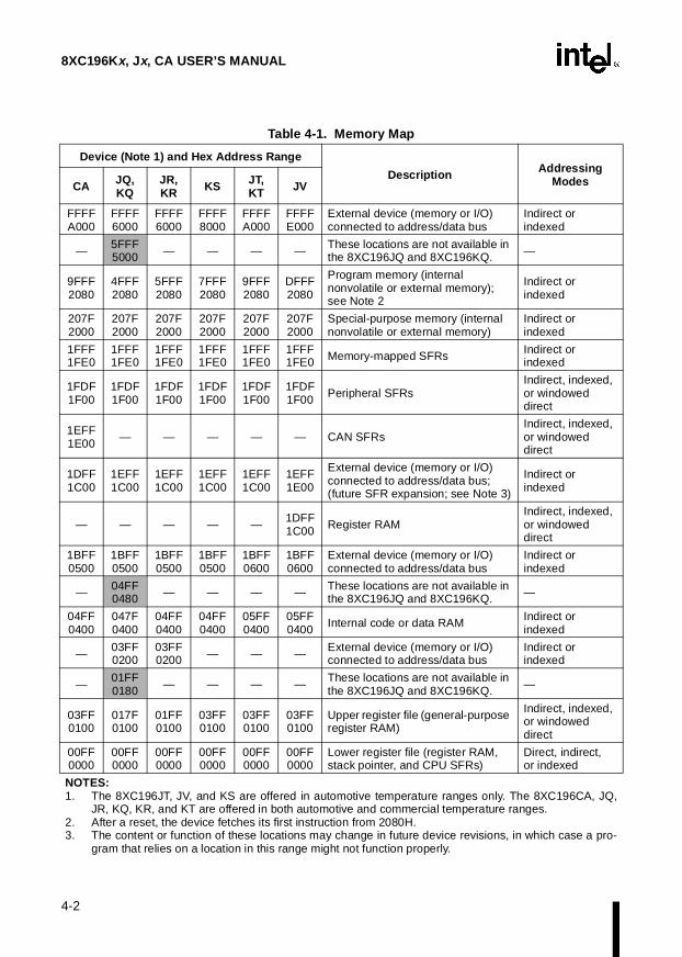
8XC196Kx, Jx, CA USER’S MANUAL
4-2
Table 4-1. Memory Map
Device (Note 1) and Hex Address Range
Description Addressing ModesCA JQ,
KQJR, KR KS JT,
KT JV
FFFFA000
FFFF6000
FFFF6000
FFFF8000
FFFFA000
FFFFE000
External device (memory or I/O) connected to address/data bus
Indirect or indexed
— 5FFF5000 — — — — These locations are not available in
the 8XC196JQ and 8XC196KQ. —
9FFF2080
4FFF2080
5FFF2080
7FFF2080
9FFF2080
DFFF2080
Program memory (internal nonvolatile or external memory); see Note 2
Indirect or indexed
207F2000
207F2000
207F2000
207F2000
207F2000
207F2000
Special-purpose memory (internal nonvolatile or external memory)
Indirect or indexed
1FFF1FE0
1FFF1FE0
1FFF1FE0
1FFF1FE0
1FFF1FE0
1FFF1FE0 Memory-mapped SFRs Indirect or
indexed
1FDF1F00
1FDF1F00
1FDF1F00
1FDF1F00
1FDF1F00
1FDF1F00 Peripheral SFRs
Indirect, indexed, or windowed direct
1EFF1E00 — — — — — CAN SFRs
Indirect, indexed, or windowed direct
1DFF1C00
1EFF1C00
1EFF1C00
1EFF1C00
1EFF1C00
1EFF1E00
External device (memory or I/O) connected to address/data bus;(future SFR expansion; see Note 3)
Indirect or indexed
— — — — — 1DFF1C00 Register RAM
Indirect, indexed, or windowed direct
1BFF0500
1BFF0500
1BFF0500
1BFF0500
1BFF0600
1BFF0600
External device (memory or I/O) connected to address/data bus
Indirect or indexed
—04FF0480 — — — — These locations are not available in
the 8XC196JQ and 8XC196KQ. —
04FF0400
047F0400
04FF0400
04FF0400
05FF0400
05FF0400 Internal code or data RAM Indirect or
indexed
— 03FF0200
03FF0200 — — — External device (memory or I/O)
connected to address/data busIndirect or indexed
— 01FF0180 — — — — These locations are not available in
the 8XC196JQ and 8XC196KQ. —
03FF0100
017F0100
01FF0100
03FF0100
03FF0100
03FF0100
Upper register file (general-purpose register RAM)
Indirect, indexed, or windowed direct
00FF0000
00FF0000
00FF0000
00FF0000
00FF0000
00FF0000
Lower register file (register RAM, stack pointer, and CPU SFRs)
Direct, indirect, or indexed
NOTES:1. The 8XC196JT, JV, and KS are offered in automotive temperature ranges only. The 8XC196CA, JQ,
JR, KQ, KR, and KT are offered in both automotive and commercial temperature ranges.2. After a reset, the device fetches its first instruction from 2080H.3. The content or function of these locations may change in future device revisions, in which case a pro-
gram that relies on a location in this range might not function properly.

4-3
MEMORY PARTITIONS
4.1.3 Program Memory
Program memory occupies a memory partition beginning at 2080H. (See Table 4-1 for the endingaddress for each device.) This entire partition is available for storing executable code and data.The EA# signal controls access to program memory. Accesses to this address range are directedto internal memory if EA# is held high and to external memory if EA# is held low. For deviceswithout internal nonvolatile memory, the EA# signal must be tied low. EA# is latched at reset.
NOTE
We recommend that you write FFH (the opcode for the RST instruction) to unused program memory locations. This causes a device reset if a program unintentionally begins to execute in unused memory.
4.1.4 Special-purpose Memory
Special-purpose memory resides in locations 2000–207FH (Table 4-2). It contains several re-served memory locations, the chip configuration bytes (CCBs), and vectors for both peripheraltransaction server (PTS) and standard interrupts. Accesses to this address range are directed tointernal memory if EA# is held high and to external memory if EA# is held low. For devices with-out internal nonvolatile memory, the EA# signal must be tied low. EA# is latched at reset.
Table 4-2. Special-purpose Memory Addresses
Hex Address Description
207F205E Reserved (each byte must contain FFH)
205D2040 PTS vectors
203F2030 Upper interrupt vectors
202F2020 Security key
201F Reserved (must contain 20H)
201E Reserved (must contain FFH)
201D Reserved (must contain 20H)
201C Reserved (must contain FFH)
201B Reserved (must contain 20H)
201A CCB1
2019 Reserved (must contain 20H)
2018 CCB0
20172016 OFD flag (see page 13-12 and page 16-8)
20152014 Reserved (each byte must contain FFH)
20132000 Lower interrupt vectors

8XC196Kx, Jx, CA USER’S MANUAL
4-4
4.1.4.1 Reserved Memory Locations
Several memory locations are reserved for testing or for use in future products. Do not read orwrite these locations except to initialize them. The function or contents of these locations maychange in future revisions; software that uses reserved locations may not function properly. Al-ways initialize reserved locations to the values listed in Table 4-2 on page 4-3.
4.1.4.2 Interrupt and PTS Vectors
The upper and lower interrupt vectors contain the addresses of the interrupt service routines. Theperipheral transaction server (PTS) vectors contain the addresses of the PTS control blocks. SeeChapter 5, “Standard and PTS Interrupts,” for more information on interrupt and PTS vectors.
4.1.4.3 Security Key
The security key prevents unauthorized programming access to the nonvolatile memory. SeeChapter 16, “Programming the Nonvolatile Memory,” for details.
4.1.4.4 Chip Configuration Bytes (CCBs)
The chip configuration bytes (CCBs) specify the operating environment. They specify the buswidth, bus-control mode, and wait states. They also control powerdown mode, the watchdog tim-er, and nonvolatile memory protection.
The CCBs are the first bytes fetched from memory when the device leaves the reset state. Thepost-reset sequence loads the CCBs into the chip configuration registers (CCRs). Once they areloaded, the CCRs cannot be changed until the next device reset. Typically, the CCBs are pro-grammed once when the user program is compiled and are not redefined during normal operation.“Chip Configuration Registers and Chip Configuration Bytes” on page 15-4 describes the CCBsand CCRs.
For devices with user-programmable nonvolatile memory, the CCBs are loaded for normal oper-ation, but the PCCBs are loaded into the CCRs if the device is entering programming modes. SeeChapter 16, “Programming the Nonvolatile Memory,” for details.

4-5
MEMORY PARTITIONS
4.1.5 Special-function Registers (SFRs)
These devices have both memory-mapped SFRs and peripheral SFRs. The memory-mappedSFRs must be accessed using indirect or indexed addressing modes, and they cannot be win-dowed. The peripheral SFRs are physically located in the on-chip peripherals, and they can bewindowed (see “Windowing” on page 4-13). Do not use reserved SFRs; write zeros to them orleave them in their default state. When read, reserved bits and reserved SFRs return undefinedvalues.
NOTE
Using any SFR as a base or index register for indirect or indexed operations can cause unpredictable results. External events can change the contents of SFRs, and some SFRs are cleared when read. For this reason, consider the implications of using an SFR as an operand in a read-modify-write instruction (e.g., XORB).
4.1.5.1 Memory-mapped SFRs
Locations 1FE0–1FFFH contain memory-mapped SFRs (see Table 4-3). Locations in this rangethat are omitted from the table are reserved. The memory-mapped SFRs must be accessed withindirect or indexed addressing modes, and they cannot be windowed. If you read a location in thisrange through a window, the SFR appears to contain FFH (all ones). If you write a location inthis range through a window, the write operation has no effect on the SFR.
The memory-mapped SFRs are accessed through the memory controller, so instructions that op-erate on these SFRs execute as they would from external memory with zero wait states.
Table 4-3. Memor y-mapped SFRs
Ports 3, 4, 5, Slave Port, UPROM SFRs
Hex Address High (Odd) Byte Low (Even) Byte
1FFE P4_PIN P3_PIN
1FFC P4_REG P3_REG
1FFA SLP_CON SLP_CMD
1FF8 Reserved SLP_STAT
1FF6 P5_PIN USFR
1FF4 P5_REG P34_DRV
1FF2 P5_DIR Reserved
1FF0 P5_MODE Reserved

8XC196Kx, Jx, CA USER’S MANUAL
4-6
4.1.5.2 Peripheral SFRs
Locations 1F00–1FDFH provide access to the peripheral SFRs (Table 4-4). Locations in thisrange that are omitted from the table are reserved. The peripheral SFRs are I/O control registers;they are physically located in the on-chip peripherals. These peripheral SFRs can be windowedand they can be addressed either as words or bytes, except as noted in Table 4-4.
The peripheral SFRs are accessed directly, without using the memory controller, so instructionsthat operate on these SFRs execute as they would if they were operating on the register file.
NOTE
Some peripheral SFRs are implemented differently in the 87C196CA, 8XC196Jx, and 8XC196Kx devices. The individual SFR descriptions throughout this manual note the differences.

4-7
MEMORY PARTITIONS
Table 4-4. Peripheral SFRsPorts 0, 1, 2, and 6 SFRs Timer 1, Timer 2, and EPA SFRs
Address High (Odd) Byte Low (Even) Byte Address High ( Odd) Byte Low (E ven) Byte
1FDEH Reserved Reserved †1F9EH TIMER2 (H) TIMER2 (L)
1FDCH Reserved Reserved 1F9CH Reserved T2CONTROL
1FDAH Reserved P0_PIN †1F9AH TIMER1 (H) TIMER1 (L)
1FD8H Reserved Reserved 1F98H Reserved T1CONTROL
1FD6H P6_PIN P1_PIN 1F96H Reserved Reserved
1FD4H P6_REG P1_REG 1F94H Reserved Reserved
1FD2H P6_DIR P1_DIR 1F92H Reserved Reserved
1FD0H P6_MODE P1_MODE 1F90H Reserved Reserved
1FCEH P2_PIN Reserved EPA SFRs
1FCCH P2_REG Reserved Address High ( Odd) Byte Low (E ven) Byte
1FCAH P2_DIR Reserved †1F8EH COMP1_TIME (H) COMP1_TIME (L)
1FC8H P2_MODE Reserved 1F8CH Reserved COMP1_CON
1FC6H Reserved Reserved †1F8AH COMP0_TIME (H) COMP0_TIME (L)
1FC4H Reserved Reserved 1F88H Reserved COMP0_CON
1FC2H Reserved Reserved †1F86H EPA9_TIME (H) EPA9_TIME (L)
1FC0H Reserved Reserved 1F84H Reserved EPA9_CON
SIO and SSIO SFRs †1F82H EPA8_TIME (H) EPA8_TIME (L)
Address High (Odd) Byte Low (Even) Byte 1F80H Reserved EPA8_CON
1FBEH Reserved Reserved †1F7EH EPA7_TIME (H) EPA7_TIME (L)
1FBCH SP_BAUD (H) SP_BAUD (L) 1F7CH Reserved EPA7_CON
1FBAH SP_CON SBUF_TX †1F7AH EPA6_TIME (H) EPA6_TIME (L)
1FB8H SP_STATUS SBUF_RX 1F78H Reserved EPA6_CON
1FB6H Reserved Reserved †1F76H EPA5_TIME (H) EPA5_TIME (L)
1FB4H Reserved SSIO_BAUD 1F74H Reserved EPA5_CON
1FB2H SSIO1_CON SSIO1_BUF †1F72H EPA4_TIME (H) EPA4_TIME (L)
1FB0H SSIO0_CON SSIO0_BUF 1F70H Reserved EPA4_CON
A/D SFRs †1F6EH EPA3_TIME (H) EPA3_TIME (L)
Address High (Odd) Byte Low (Even) Byte †1F6CH EPA3_CON (H) EPA3_CON (L)
1FAEH AD_TIME AD_TEST †1F6AH EPA2_TIME (H) EPA2_TIME (L)
1FACH Reserved AD_COMMAND 1F68H Reserved EPA2_CON
1FAAH AD_RESULT (H) AD_RESULT (L) †1F66H EPA1_TIME (H) EPA1_TIME (L)
EPA Interrupt SFRs †1F64H EPA1_CON (H) EPA1_CON (L)
Address High (Odd) Byte Low (Even) Byte †1F62H EPA0_TIME (H) EPA0_TIME (L)
1FA8H Reserved EPAIPV 1F60H Reserved EPA0_CON
1FA6H Reserved EPA_PEND1
1FA4H Reserved EPA_MASK1†1FA2H EPA_PEND (H) EPA_PEND (L)†1FA0H EPA_MASK (H) EPA_MASK (L)
† Must be addressed as a word.

8XC196Kx, Jx, CA USER’S MANUAL
4-8
Table 4-5. CAN Peripheral SFRs — 8XC196CA Only Message 15 Message 11
Addr High (Odd) Byte Low (Even) Byte Addr High ( Odd) Byte Low (Even) Byte
1EFEH Reserved CAN_MSG15DATA7 1EBEH Reserved CAN_MSG11DATA7
1EFCH CAN_MSG15DATA6 CAN_MSG15DATA5 1EBCH CAN_MSG11DATA6 CAN_MSG11DATA5
1EFAH CAN_MSG15DATA4 CAN_MSG15DATA3 1EBAH CAN_MSG11DATA4 CAN_MSG11DATA3
1EF8H CAN_MSG15DATA2 CAN_MSG15DATA1 1EB8H CAN_MSG11DATA2 CAN_MSG11DATA1
1EF6H CAN_MSG15DATA0 CAN_MSG15CFG 1EB6H CAN_MSG11DATA0 CAN_MSG11CFG
1EF4H CAN_MSG15ID3 CAN_MSG15ID2 1EB4H CAN_MSG11ID3 CAN_MSG11ID2
1EF2H CAN_MSG15ID1 CAN_MSG15ID0 1EB2H CAN_MSG11ID1 CAN_MSG11ID0
1EF0H CAN_MSG15CON1 CAN_MSG15CON0 1EB0H CAN_MSG11CON1 CAN_MSG11CON0
Message 14 Message 10
Addr High (Odd) Byte Low (Even) Byte Addr High ( Odd) Byte Low (Even) Byte
1EEEH Reserved CAN_MSG14DATA7 1EAEH Reserved CAN_MSG10DATA7
1EECH CAN_MSG14DATA6 CAN_MSG14DATA5 1EACH CAN_MSG10DATA6 CAN_MSG10DATA5
1EEAH CAN_MSG14DATA4 CAN_MSG14DATA3 1EAAH CAN_MSG10DATA4 CAN_MSG10DATA3
1EE8H CAN_MSG14DATA2 CAN_MSG14DATA1 1EA8H CAN_MSG10DATA2 CAN_MSG10DATA1
1EE6H CAN_MSG14DATA0 CAN_MSG14CFG 1EA6H CAN_MSG10DATA0 CAN_MSG10CFG
1EE4H CAN_MSG14ID3 CAN_MSG14ID2 1EA4H CAN_MSG10ID3 CAN_MSG10ID2
1EE2H CAN_MSG14ID1 CAN_MSG14ID0 1EA2H CAN_MSG10ID1 CAN_MSG10ID0
1EE0H CAN_MSG14CON1 CAN_MSG14CON0 1EA0H CAN_MSG10CON1 CAN_MSG10CON0
Message 13 Message 9
Addr High (Odd) Byte Low (Even) Byte Addr High ( Odd) Byte Low (Even) Byte
1EDEH Reserved CAN_MSG13DATA7 1E9EH Reserved CAN_MSG9DATA7
1EDCH CAN_MSG13DATA6 CAN_MSG13DATA5 1E9CH CAN_MSG9DATA6 CAN_MSG9DATA5
1EDAH CAN_MSG13DATA4 CAN_MSG13DATA3 1E9AH CAN_MSG9DATA4 CAN_MSG9DATA3
1ED8H CAN_MSG13DATA2 CAN_MSG13DATA1 1E98H CAN_MSG9DATA2 CAN_MSG9DATA1
1ED6H CAN_MSG13DATA0 CAN_MSG13CFG 1E96H CAN_MSG9DATA0 CAN_MSG9CFG
1ED4H CAN_MSG13ID3 CAN_MSG13ID2 1E94H CAN_MSG9ID3 CAN_MSG9ID2
1ED2H CAN_MSG13ID1 CAN_MSG13ID0 1E92H CAN_MSG9ID1 CAN_MSG9ID0
1ED0H CAN_MSG13CON1 CAN_MSG13CON0 1E90H CAN_MSG9CON1 CAN_MSG9CON0
Message 12 Message 8
Addr High (Odd) Byte Low (Even) Byte Addr High ( Odd) Byte Low (Even) Byte
1ECEH Reserved CAN_MSG12DATA7 1E8EH Reserved CAN_MSG8DATA7
1ECCH CAN_MSG12DATA6 CAN_MSG12DATA5 1E8CH CAN_MSG8DATA6 CAN_MSG8DATA5
1ECAH CAN_MSG12DATA4 CAN_MSG12DATA3 1E8AH CAN_MSG8DATA4 CAN_MSG8DATA3
1EC8H CAN_MSG12DATA2 CAN_MSG12DATA1 1E88H CAN_MSG8DATA2 CAN_MSG8DATA1
1EC6H CAN_MSG12DATA0 CAN_MSG12CFG 1E86H CAN_MSG8DATA0 CAN_MSG8CFG
1EC4H CAN_MSG12ID3 CAN_MSG12ID2 1E84H CAN_MSG8ID3 CAN_MSG8ID2
1EC2H CAN_MSG12ID1 CAN_MSG12ID0 1E82H CAN_MSG8ID1 CAN_MSG8ID0
1EC0H CAN_MSG12CON1 CAN_MSG12CON0 1E80H CAN_MSG8CON1 CAN_MSG8CON0
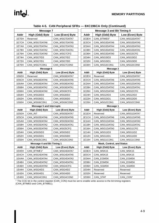
4-9
MEMORY PARTITIONS
Message 7 Message 3 and Bit Timing 0
Addr High (Odd) Byte Low (Even) Byte Addr High (Odd) Byte Low (Even) Byte1E7EH Reserved CAN_MSG7DATA7 1E3EH CAN_BTIME0† CAN_MSG3DATA7
1E7CH CAN_MSG7DATA6 CAN_MSG7DATA5 1E3CH CAN_MSG3DATA6 CAN_MSG3DATA5
1E7AH CAN_MSG7DATA4 CAN_MSG7DATA3 1E3AH CAN_MSG3DATA4 CAN_MSG3DATA3
1E78H CAN_MSG7DATA2 CAN_MSG7DATA1 1E38H CAN_MSG3DATA2 CAN_MSG3DATA1
1E76H CAN_MSG7DATA0 CAN_MSG7CFG 1E36H CAN_MSG3DATA0 CAN_MSG3CFG
1E74H CAN_MSG7ID3 CAN_MSG7ID2 1E34H CAN_MSG3ID3 CAN_MSG3ID2
1E72H CAN_MSG7ID1 CAN_MSG7ID0 1E32H CAN_MSG3ID1 CAN_MSG3ID0
1E70H CAN_MSG7CON1 CAN_MSG7CON0 1E30H CAN_MSG3CON1 CAN_MSG3CON0
Message 6 Message 2
Addr High (Odd) Byte Low (Even) Byte Addr High ( Odd) Byte Low (Even) Byte
1E6EH Reserved CAN_MSG6DATA7 1E2EH Reserved CAN_MSG2DATA7
1E6CH CAN_MSG6DATA6 CAN_MSG6DATA5 1E2CH CAN_MSG2DATA6 CAN_MSG2DATA5
1E6AH CAN_MSG6DATA4 CAN_MSG6DATA3 1E2AH CAN_MSG2DATA4 CAN_MSG2DATA3
1E68H CAN_MSG6DATA2 CAN_MSG6DATA1 1E28H CAN_MSG2DATA2 CAN_MSG2DATA1
1E66H CAN_MSG6DATA0 CAN_MSG6CFG 1E26H CAN_MSG2DATA0 CAN_MSG2CFG
1E64H CAN_MSG6ID3 CAN_MSG6ID2 1E24H CAN_MSG2ID3 CAN_MSG2ID2
1E62H CAN_MSG6ID1 CAN_MSG6ID0 1E22H CAN_MSG2ID1 CAN_MSG2ID0
1E60H CAN_MSG6CON1 CAN_MSG6CON0 1E20H CAN_MSG2CON1 CAN_MSG2CON0
Message 5 and Interrupts Message 1
Addr High (Odd) Byte Low (Even) Byte Addr High ( Odd) Byte Low (Even) Byte
1E5EH CAN_INT CAN_MSG5DATA7 1E1EH Reserved CAN_MSG1DATA7
1E5CH CAN_MSG5DATA6 CAN_MSG5DATA5 1E1CH CAN_MSG1DATA6 CAN_MSG1DATA5
1E5AH CAN_MSG5DATA4 CAN_MSG5DATA3 1E1AH CAN_MSG1DATA4 CAN_MSG1DATA3
1E58H CAN_MSG5DATA2 CAN_MSG5DATA1 1E18H CAN_MSG1DATA2 CAN_MSG1DATA1
1E56H CAN_MSG5DATA0 CAN_MSG5CFG 1E16H CAN_MSG1DATA0 CAN_MSG1CFG
1E54H CAN_MSG5ID3 CAN_MSG5ID2 1E14H CAN_MSG1ID3 CAN_MSG1ID2
1E52H CAN_MSG5ID1 CAN_MSG5ID0 1E12H CAN_MSG1ID1 CAN_MSG1ID0
1E50H CAN_MSG5CON1 CAN_MSG5CON0 1E10H CAN_MSG1CON1 CAN_MSG1CON0
Message 4 and Bit Timing 1 Mask, Control, and Status
Addr High (Odd) Byte Low (Even) Byte Addr High ( Odd) Byte Low (Even) Byte
1E4EH CAN_BTIME1† CAN_MSG4DATA7 1E0EH CAN_MSK15 CAN_MSK15
1E4CH CAN_MSG4DATA6 CAN_MSG4DATA5 1E0CH CAN_MSK15 CAN_MSK15
1E4AH CAN_MSG4DATA4 CAN_MSG4DATA3 1E0AH CAN_EGMSK CAN_EGMSK
1E48H CAN_MSG4DATA2 CAN_MSG4DATA1 1E08H CAN_EGMSK CAN_EGMSK
1E46H CAN_MSG4DATA0 CAN_MSG4CFG 1E06H CAN_SGMSK CAN_SGMSK
1E44H CAN_MSG4ID3 CAN_MSG4ID2 1E04H Reserved Reserved
1E42H CAN_MSG4ID1 CAN_MSG4ID0 1E02H Reserved Reserved
1E40H CAN_MSG4CON1 CAN_MSG4CON0 1E00H CAN_STAT CAN_CON†
† The CCE bit in the control register (CAN_CON) must be set to enable write access to the bit timing registers (CAN_BTIME0 and CAN_BTIME1).
Table 4-5. CAN Peripheral SFRs — 8XC196CA Only (Continued)

8XC196Kx, Jx, CA USER’S MANUAL
4-10
4.1.6 Internal RAM (Code RAM)
These devices have up to 512 bytes of internal RAM (see Table 4-1 on page 4-2 for details) be-ginning at location 0400H. Although it is sometimes called code RAM to distinguish it from reg-ister RAM, this internal RAM can store either executable code or data. The code RAM is accessedthrough the memory controller, so code executes as it would from external memory with zero waitstates. Data stored in this area must be accessed with indirect or indexed addressing, so data ac-cesses to this area take longer than data accesses to the register RAM. The code RAM cannot bewindowed.
4.1.7 Register File
The register file (Figure 4-1) is divided into an upper register file and a lower register file. Theupper register file consists of general-purpose register RAM. The lower register file contains gen-eral-purpose register RAM along with the stack pointer (SP) and the CPU special-function regis-ters (SFRs).
Table 4-1 on page 4-2 lists the register file memory addresses. The RALU accesses the lower reg-ister file directly, without the use of the memory controller. It also accesses a windowed locationdirectly (see “Windowing” on page 4-13). The upper register file and the peripheral SFRs can bewindowed. The 8XC196JV has additional register RAM in locations 1C00–1DFFH. Like thegeneral-purpose register RAM in the upper register file, this register RAM can be windowed andis accessed directly, without the use of the memory controller. Registers in the lower register fileand registers being windowed can be accessed with register-direct addressing.
NOTE
The register file must not contain code. An attempt to execute an instruction from a location in the register file causes the memory controller to fetch the instruction from external memory.

4-11
MEMORY PARTITIONS
Figure 4-1. Register File Memory Map
Table 4-6. Register File Memory Addresses
Device and Hex Address Range
Description Addressing ModesJV CA, JT,
KS, KT JR, KR JQ, KQ
1DFF1C00 — — — Register RAM Indirect, indexed, or windowed
direct
03FF0100
03FF0100
01FF0100
017F0100 Upper register file (register RAM) Indirect, indexed, or windowed
direct
00FF001A
00FF001A
00FF001A
00FF001A Lower register file (register RAM) Direct, indirect, or indexed
00190018
00190018
00190018
00190018 Lower register file (stack pointer) Direct, indirect, or indexed
00170000
00170000
00170000
00170000 Lower register file (CPU SFRs) Direct, indirect, or indexed
Upper Register File
Lower
Register File
03FFH
0100H 00FFH
0000H
Address
A3073-02
01FFH (JR, KR) 017FH (JQ, KQ) 0100H 00FFH 001AH 0019H 0018H 0017H 0000H
General-purpose Register RAM
Stack Pointer
General-purpose Register RAM
CPU SFRs
03FFH (CA, JT, JV, KS, KT)
Address
8XC196Kx, Jx, CA USER’S MANUAL
4-12
4.1.7.1 General-pur pose Register RAM
The lower register file contains general-purpose register RAM. The stack pointer locations canalso be used as general-purpose register RAM when stack operations are not being performed.The RALU can access this memory directly, using register-direct addressing.
The upper register file also contains general-purpose register RAM. The RALU normally usesindirect or indexed addressing to access the RAM in the upper register file. Windowing enablesthe RALU to use register-direct addressing to access this memory. (See Chapter 3, “ProgrammingConsiderAtions,” for a discussion of addressing modes.) Windowing can provide for fast contextswitching of interrupt tasks and faster program execution. (See “Windowing” on page 4-13.) PTScontrol blocks and the stack are most efficient when located in the upper register file.
The 8XC196JV has additional register RAM in locations 1C00–1DFFH. Like the general-pur-pose register RAM in the upper register file, this register RAM can be windowed and is accesseddirectly, without the use of the memory controller.
4.1.7.2 Stack Pointer (SP)
Memory locations 0018H and 0019H contain the stack pointer (SP). The SP contains the addressof the stack. The SP must point to a word (even) address that is two bytes greater than the desiredstarting address. Before the CPU executes a subroutine call or interrupt service routine, it decre-ments the SP by two and copies (PUSHes) the address of the next instruction from the programcounter onto the stack. It then loads the address of the subroutine or interrupt service routine intothe program counter. When it executes the return-from-subroutine (RET) instruction at the end ofthe subroutine or interrupt service routine, the CPU loads (POPs) the contents of the top of thestack (that is, the return address) into the program counter and increments the SP by two.
Subroutines may be nested. That is, each subroutine may call other subroutines. The CPUPUSHes the contents of the program counter onto the stack each time it executes a subroutine call.The stack grows downward as entries are added. The only limit to the nesting depth is the amountof available memory. As the CPU returns from each nested subroutine, it POPs the address offthe top of the stack, and the next return address moves to the top of the stack.
Your program must load a word-aligned (even) address into the stack pointer. Select an addressthat is two bytes greater than the desired starting address because the CPU automatically decre-ments the stack pointer before it pushes the first byte of the return address onto the stack. Remem-ber that the stack grows downward, so allow sufficient room for the maximum number of stackentries. The stack must be located in either the internal register file or external RAM. The stackcan be used most efficiently when it is located in the register file.

4-13
MEMORY PARTITIONS
The following example initializes the top of the upper register file (8XC196CA, JT, JV, KS, KT)as the stack. (For the 8XC196JR or KR, the immediate value would be #200H; for the 8XC196JQor KQ, it would be #180H.)
LD SP, #400H ;Load stack pointer
The following example shows how to allow the linker locator to determine where the stack fitsin the memory map that you specify.
LD SP, #STACK
4.1.7.3 CPU Special-function Registers (SFRs)
Locations 0000–0017H in the lower register file are the CPU SFRs (Table 4-7). Appendix C de-scribes the CPU SFRs.
NOTE
Using any SFR as a base or index register for indirect or indexed operations can cause unpredictable results. External events can change the contents of SFRs, and some SFRs are cleared when read. For this reason, consider the implications of using an SFR as an operand in a read-modify-write instruction (e.g., XORB).
4.2 WINDOWING
Windowing expands the amount of memory that is accessible with register-direct addressing.Register-direct addressing can access the lower register file with short, fast-executing instruc-tions. With windowing, register-direct addressing can also access the upper register file and pe-ripheral SFRs.
Table 4-7. CPU SFRs
Address High (Odd) Byte Low (Even) Byte
0016H Reserved Reserved
0014H Reserved WSR
0012H INT_MASK1 INT_PEND1
0010H Reserved Reserved
000EH Reserved Reserved
000CH Reserved Reserved
000AH Reserved WATCHDOG
0008H INT_PEND INT_MASK
0006H PTSSRV (H) PTSSRV (L)
0004H PTSSEL (H) PTSSEL (L)
0002H ONES_REG (H) ONES_REG (L)
0000H ZERO_REG (H) ZERO_REG (L)

8XC196Kx, Jx, CA USER’S MANUAL
4-14
Windowing maps a segment of higher memory (the upper register file or peripheral SFRs) intothe lower register file. The window selection register (WSR) selects a 32-, 64-, or 128-byte seg-ment of higher memory to be windowed into the top of the lower register file space. Figure 4-2shows the upper register file of the 8XC196CA, JT, JV, KS, and KT devices. Please refer to Table4-1 on page 4-2 for the upper register file addresses for other devices.
The 8XC196JV has additional register RAM in locations 1C00–1DFFH. Like the general-pur-pose register RAM in the upper register file, this register RAM can be windowed and is accesseddirectly, without the use of the memory controller.
Figure 4-2. Windowing
NOTE
Memory-mapped SFRs must be accessed using indirect or indexed addressing modes; they cannot be windowed. Reading a memory-mapped SFR through a window returns FFH (all ones). Writing to a memory-mapped SFR through a window has no effect.
4.2.1 Selecting a Window
The window selection register (Figure 4-3) has two functions. The HLDEN bit (WSR.7) enablesand disables the bus-hold protocol (see Chapter 15, “Interfacing with External Memory”); it isunrelated to windowing. The remaining bits select a window to be mapped into the top of the low-er register file.
03FFH
0380H
00FFH
0080H
A3060-01
128-byte Window (WSR = 17H)
Window in Lower Register File
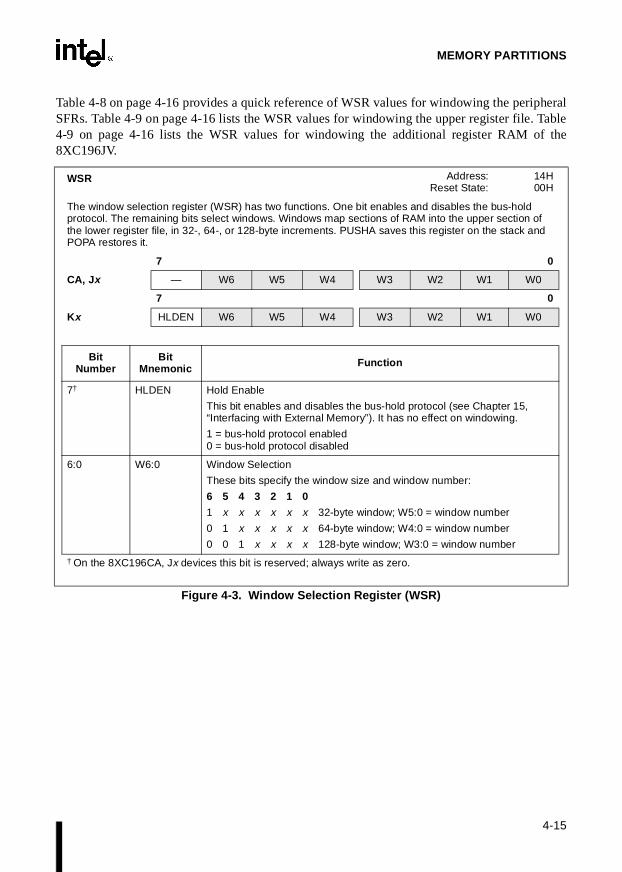
4-15
MEMORY PARTITIONS
Table 4-8 on page 4-16 provides a quick reference of WSR values for windowing the peripheralSFRs. Table 4-9 on page 4-16 lists the WSR values for windowing the upper register file. Table4-9 on page 4-16 lists the WSR values for windowing the additional register RAM of the8XC196JV.
WSR Address:Reset State:
14H00H
The window selection register (WSR) has two functions. One bit enables and disables the bus-hold protocol. The remaining bits select windows. Windows map sections of RAM into the upper section of the lower register file, in 32-, 64-, or 128-byte increments. PUSHA saves this register on the stack and POPA restores it.
7 0
CA, Jx — W6 W5 W4 W3 W2 W1 W0
7 0
Kx HLDEN W6 W5 W4 W3 W2 W1 W0
BitNumber
BitMnemonic Function
7† HLDEN Hold Enable
This bit enables and disables the bus-hold protocol (see Chapter 15, “Interfacing with External Memory”). It has no effect on windowing.
1 = bus-hold protocol enabled0 = bus-hold protocol disabled
6:0 W6:0 Window Selection
These bits specify the window size and window number:
6 5 4 3 2 1 0
1 x x x x x x 32-byte window; W5:0 = window number
0 1 x x x x x 64-byte window; W4:0 = window number
0 0 1 x x x x 128-byte window; W3:0 = window number
† On the 8XC196CA, Jx devices this bit is reserved; always write as zero.
Figure 4-3. Window Selection Register (WSR)
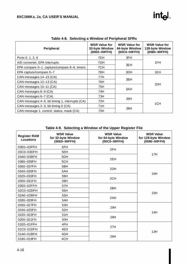
8XC196Kx, Jx, CA USER’S MANUAL
4-16
Table 4-8. Selecting a Window of Peripheral SFRs
PeripheralWSR Value for
32-byte Window(00E0–00FFH)
WSR Value for 64-byte Window(00C0–00FFH)
WSR Value for 128-byte Window
(0080–00FFH)
Ports 0, 1, 2, 6 7EH 3FH
1FHA/D converter, EPA interrupts 7DH3EH
EPA compare 0–1, capture/compare 8–9, timers 7CH
EPA capture/compare 0–7 7BH 3DH 1EH
CAN messages 14–15 (CA) 77H3BH
1DHCAN messages 12–13 (CA) 76H
CAN messages 10–11 (CA) 75H3AH
CAN messages 8–9 (CA) 74H
CAN messages 6–7 (CA) 73H39H
1CHCAN messages 4–5, bit timing 1, interrupts (CA) 72H
CAN messages 2–3, bit timing 0 (CA) 71H38H
CAN message 1, control, status, mask (CA) 70H
Table 4-9. Selecting a Window of the Upper Register File
Register RAMLocations
WSR Value for 32-byte Window
(00E0–00FFH)
WSR Valuefor 64-byte Window
(00C0–00FFH)
WSR Value for 128-byte Window
(0080–00FFH)
03E0–03FFH 5FH2FH
17H03C0–03DFH 5EH
03A0–03BFH 5DH2EH
0380–039FH 5CH
0360–037FH 5BH2DH
16H0340–035FH 5AH
0320–033FH 59H2CH
0300–031FH 58H
02E0–02FFH 57H2BH
15H02C0–02DFH 56H
02A0–02BFH 55H2AH
0280–029FH 54H
0260–027FH 53H29H
14H0240–025FH 52H
0220–023FH 51H28H
0200–021FH 50H
01E0–01FFH 4FH27H
13H01C0–01DFH 4EH
01A0–01BFH 4DH26H
0180–019FH 4CH

4-17
MEMORY PARTITIONS
4.2.2 Addressing a Location Through a Window
After you have selected the desired window, you need to know the windowed direct address ofthe memory location (the address in the lower register file). Calculate the windowed direct ad-dress as follows:
1. Subtract the base address of the area to be remapped (from Table 4-11 on page 4-18) fromthe address of the desired location. This gives you the offset of that particular location.
2. Add the offset to the base address of the window (from Table 4-12 on page 4-20). Theresult is the windowed direct address.
0160–017FH 4BH25H
12H0140–015FH 4AH
0120–013FH 49H24H
0100–011FH 48H
Table 4-10. Selecting a Window of Upper Register RAM — 8XC196JV Only
Register RAMLocations
WSR Value for 32-byte Window
(00E0–00FFH)
WSR Valuefor 64-byte Window
(00C0–00FFH)
WSR Value for 128-byte Window
(0080–00FFH)
0DE0–0DFFH 6FH37H
1BH0DC0–0DDFH 6EH
0DA0–0DBFH 6DH36H
0D80–0D9FH 6CH
0D60–0D7FH 6BH35H
1AH0D40–0D5FH 6AH
0D20–0D3FH 69H34H
0D00–0D1FH 68H
0CE0–0CFFH 67H33H
19H0CC0–0CDFH 66H
0CA0–0CBFH 65H32H
0C80–0C9FH 64H
0C60–0C7FH 63H31H
18H0C40–0C5FH 62H
0C20–0C3FH 61H30H
0C00–0C1FH 60H
Table 4-9. Selecting a Window of the Upper Register File (Continued)
Register RAMLocations
WSR Value for 32-byte Window
(00E0–00FFH)
WSR Valuefor 64-byte Window
(00C0–00FFH)
WSR Value for 128-byte Window
(0080–00FFH)
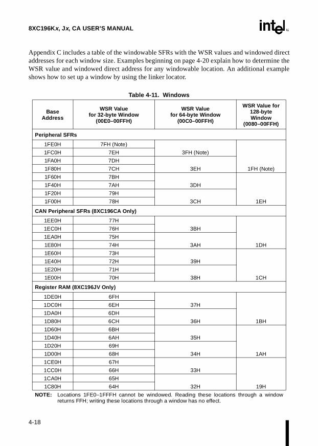
8XC196Kx, Jx, CA USER’S MANUAL
4-18
Appendix C includes a table of the windowable SFRs with the WSR values and windowed directaddresses for each window size. Examples beginning on page 4-20 explain how to determine theWSR value and windowed direct address for any windowable location. An additional exampleshows how to set up a window by using the linker locator.
Table 4-11. Windows
Base Address
WSR Value for 32-byte Window
(00E0–00FFH)
WSR Valuefor 64-byte Window
(00C0–00FFH)
WSR Value for 128-byte Window
(0080–00FFH)
Peripheral SFRs
1FE0H 7FH (Note)
3FH (Note)
1FH (Note)
1FC0H 7EH
1FA0H 7DH
3EH1F80H 7CH
1F60H 7BH
3DH
1EH
1F40H 7AH
1F20H 79H
3CH1F00H 78H
CAN Peripheral SFRs (8XC196CA Only)
1EE0H 77H
3BH
1DH
1EC0H 76H
1EA0H 75H
3AH1E80H 74H
1E60H 73H
39H
1CH
1E40H 72H
1E20H 71H
38H1E00H 70H
Register RAM (8XC196JV Only)
1DE0H 6FH
37H
1BH
1DC0H 6EH
1DA0H 6DH
36H1D80H 6CH
1D60H 6BH
35H
1AH
1D40H 6AH
1D20H 69H
34H1D00H 68H
1CE0H 67H
33H
19H
1CC0H 66H
1CA0H 65H
32H1C80H 64H
NOTE: Locations 1FE0–1FFFH cannot be windowed. Reading these locations through a windowreturns FFH; writing these locations through a window has no effect.
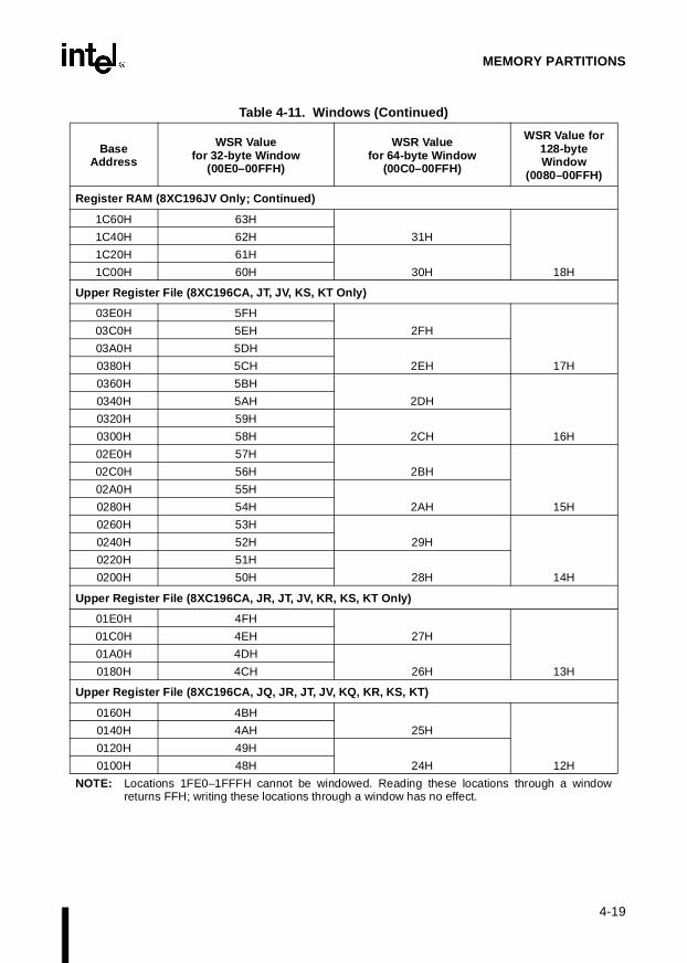
4-19
MEMORY PARTITIONS
Register RAM (8XC196JV Only; Continued)
1C60H 63H
31H
18H
1C40H 62H
1C20H 61H
30H1C00H 60H
Upper Register File (8XC196CA, JT, JV, KS, KT Only)
03E0H 5FH
2FH
17H
03C0H 5EH
03A0H 5DH
2EH0380H 5CH
0360H 5BH
2DH
16H
0340H 5AH
0320H 59H
2CH0300H 58H
02E0H 57H
2BH
15H
02C0H 56H
02A0H 55H
2AH0280H 54H
0260H 53H
29H
14H
0240H 52H
0220H 51H
28H0200H 50H
Upper Register File (8XC196CA, JR, JT, JV, KR, KS, KT Only)
01E0H 4FH
27H
13H
01C0H 4EH
01A0H 4DH
26H0180H 4CH
Upper Register File (8XC196CA, JQ, JR, JT, JV, KQ, KR, KS, KT)
0160H 4BH
25H
12H
0140H 4AH
0120H 49H
24H0100H 48H
Table 4-11. Windows (Continued)
Base Address
WSR Value for 32-byte Window
(00E0–00FFH)
WSR Valuefor 64-byte Window
(00C0–00FFH)
WSR Value for 128-byte Window
(0080–00FFH)
NOTE: Locations 1FE0–1FFFH cannot be windowed. Reading these locations through a windowreturns FFH; writing these locations through a window has no effect.

8XC196Kx, Jx, CA USER’S MANUAL
4-20
Appendix C includes a table of the windowable SFRs with the WSR values and direct addressesfor each window size. The following examples explain how to determine the WSR value and di-rect address for any windowable location. An additional example shows how to set up a windowby using the linker locator.
4.2.2.1 32-byte Windowing Example
Assume that you wish to access location 014BH (a location in the upper register file used for gen-eral-purpose register RAM) with register-direct addressing through a 32-byte window. Table 4-11on page 4-18 shows that you need to write 4AH to the window selection register. It also showsthat the base address of the 32-byte memory area is 0140H. To determine the offset, subtract thatbase address from the address to be accessed (014BH – 0140H = 000BH). Add the offset to thebase address of the window in the lower register file (00E0H, from Table 4-12). The direct ad-dress is 00EBH (000BH + 00E0H)
4.2.2.2 64-byte Windowing Example
Assume that you wish to access the COMP1_CON register (location 1F8CH) with register-directaddressing through a 64-byte window. Table 4-11 on page 4-18 shows that you need to write 3EHto the window selection register. It also shows that the base address of the 64-byte memory areais 1F80H. To determine the offset, subtract that base address from the address to be accessed(1F8CH – 1F80H = 000CH). Add the offset to the base address of the window in the lower reg-ister file (00C0H, from Table 4-12). The direct address is 00CCH (000CH + 00C0H).
4.2.2.3 128-byte Windowing Example
Assume that you wish to access location 1F82H (the EPA8_TIME register) with register-directaddressing through a 128-byte window. Table 4-11 on page 4-18 shows that you need to write1FH to the window selection register. It also shows that the base address of the 128-byte memoryarea is 1F80H. To determine the offset, subtract that base address from the address to be accessed(1F82H – 1F80H = 0002H). Add the offset to the base address of the window in the lower registerfile (0080H, from Table 4-12). The direct address is 0082H (0002H + 0080H).
Table 4-12. Windowed Base Addresses
Window Size WSR Windowed Base Address(Base Address in Lower Register File)
32-byte 00E0H
64-byte 00C0H
128-byte 0080H

4-21
MEMORY PARTITIONS
4.2.2.4 Unsupported Locations Windowing Example
Assume that you wish to access location 1FF1H (the P5_MODE register, a memory-mappedSFR) with register-direct addressing through a 128-byte window. This location is in the range ofaddresses (1FE0–1FFFH) that cannot be windowed. Although you could set up the window bywriting 1FH to the WSR, reading this location through the window would return FFH (all ones)and writing to it would not change the contents. However, you could access the peripheral SFRsin the range of 1F80–1FDFH with their windowed direct addresses.
4.2.2.5 Using the Linker Locator to Set Up a Window
In this example, the linker locator is used to set up a window. The linker locator locates the win-dow in the upper register file and determines the value to load in the WSR for access to that win-dow. (Please consult the manual provided with the linker locator for details.)
********* mod1 **************mod1 module main ;Main module for linkerpublic function1extrn ?WSR ;Must declare ?WSR as external
wsr equ 14h:bytesp equ 18h:word
oseg var1: dsw 1 ;Allocate variables in an var2: dsw 1 ;overlayable segment var3: dsw 1
cseg
function1: push wsr ;Prolog code for wsr ldb wsr, #?WSR ;Prolog code for wsr
add var1, var2, var3 ;Use the variables as registers ; ; ;
ldb wsr, [sp] ;Epilog code for wsr add sp, #2 ;Epilog code for wsr retend
******** mod2 **************

8XC196Kx, Jx, CA USER’S MANUAL
4-22
public function2extrn ?WSR
wsr equ 14h:bytesp equ 18h:word
oseg var1: dsw 1 var2: dsw 1 var3: dsw 1
cseg
function2: push wsr ;Prolog code for wsr ldb wsr, #?WSR ;Prolog code for wsr
add var1, var2, var3 ; ; ;
ldb wsr, [sp] ;Epilog code for wsr add sp, #2 ;Epilog code for wsr retend******************************
The following is an example of a linker invocation to link and locate the modules and to deter-mine the proper windowing. (This example assumes an 8XC196CA, JT, JV, KS, or KT.)
RL196 MOD1.OBJ, MOD2.OBJ registers(100h-03ffh) windowsize(32)
The above linker controls tell the linker to use registers 0100–03FFH for windowing and to usea window size of 32 bytes. (These two controls enable windowing.)
The following is the map listing for the resultant output module (MOD1 by default):
SEGMENT MAP FOR mod1(MOD1):
TYPE BASE LENGTH ALIGNMENT MODULE NAME ---- ---- ------ --------- -----------**RESERVED* 0000H 001AH STACK 001AH 0006H WORD*** GAP *** 0020H 00E0H OVRLY 0100H 0006H WORD MOD2 OVRLY 0106H 0006H WORD MOD1*** GAP *** 010CH 1F74H CODE 2080H 0011H BYTE MOD2 CODE 2091H 0011H BYTE MOD1*** GAP *** 20A2H DF5EH

4-23
MEMORY PARTITIONS
This listing shows the disassembled code:
2080H ;C814 | PUSH WSR2082H ;B14814 | LDB WSR,#48H2085H ;44E4E2E0 | ADD E0H,E2H,E4H2089H ;B21814 | LDB WSR,[SP]208CH ;65020018 | ADD SP,#02H2090H ;F0 | RET2091H ;C814 | PUSH WSR2093H ;B14814 | LDB WSR,#48H2096H ;44EAE8E6 | ADD E6H,E8H,EAH209AH ;B21814 | LDB WSR,[SP]209DH ;65020018 | ADD SP,#02H20A1H ;F0 | RET
The C compiler can also take advantage of this feature if the “windows” switch is enabled. Fordetails, see the MCS 96 microcontroller architecture software products in the Development ToolsHandbook.
4.2.3 Windowing and Addressing Modes
Once windowing is enabled, the windowed locations can be accessed both through the windowusing direct (8-bit) addressing and by the usual 16-bit addressing. The lower register file locationsthat are covered by the window are always accessible by indirect or indexed operations. To re-enable direct access to the entire lower register file, clear the WSR. To enable direct access to aparticular location in the lower register file, you can select a smaller window that does not coverthat location.
When windowing is enabled:
• a register-direct instruction that uses an address within the lower register file actuallyaccesses the window in the upper register file;
• an indirect, indexed, or zero-register instruction that uses an address within either the lowerregister file or the upper register file accesses the actual location in memory.
The following sample code illustrates the difference between register-direct and indexed address-ing when using windowing.
PUSHA ; pushes the contents of WSR onto the stackLDB WSR, #12H ; select window 12H, a 128-byte block
; The next instruction uses register-direct addrADD 40H, 80H ; mem_word(40H) ←mem_word(40H) + mem_word(380H)
; The next two instructions use indirect addrADD 40H, 80H[0] ; mem_word(40H) ←mem_word(40H) + mem_word(80H +0)ADD 40H, 380H[0] ; mem_word(40H) ←mem_word(40H) + mem_word(380H +0)POPA ; reloads the previous contents into WSR


5Standard and PTS Interrupts


5-1
CHAPTER 5STANDARD AND PTS INTERRUPTS
This chapter describes the interrupt control circuitry, priority scheme, and timing for standard andperipheral transaction server (PTS) interrupts. It discusses the three special interrupts and the fivePTS modes, two of which are used with the EPA to produce pulse-width modulated (PWM) out-puts. It also explains interrupt programming and control.
5.1 OVERVIEW
The interrupt control circuitry within a microcontroller permits real-time events to control pro-gram flow. When an event generates an interrupt, the device suspends the execution of currentinstructions while it performs some service in response to the interrupt. When the interrupt is ser-viced, program execution resumes at the point where the interrupt occurred. An internal periph-eral, an external signal, or an instruction can request an interrupt. In the simplest case, the devicereceives the request, performs the service, and returns to the task that was interrupted.
This microcontroller’s flexible interrupt-handling system has two main components: the pro-grammable interrupt controller and the peripheral transaction server (PTS). The programmableinterrupt controller has a hardware priority scheme that can be modified by your software. Inter-rupts that go through the interrupt controller are serviced by interrupt service routines that youprovide. The upper and lower interrupt vectors in special-purpose memory (see Chapter 4,“Memory Partitions”) contain the interrupt service routines’ addresses. The peripheral transac-tion server (PTS), a microcoded hardware interrupt processor, provides high-speed, low-over-head interrupt handling; it does not modify the stack or the PSW. You can configure mostinterrupts (except NMI, trap, and unimplemented opcode) to be serviced by the PTS instead ofthe interrupt controller.
The PTS supports five special microcoded routines that enable it to complete specific tasks inmuch less time than an equivalent interrupt service routine can. It can transfer bytes or words,either individually or in blocks, between any memory locations; manage multiple analog-to-dig-ital (A/D) conversions; and generate pulse-width modulated (PWM) signals. PTS interrupts havea higher priority than standard interrupts and may temporarily suspend interrupt service routines.
A block of data called the PTS control block (PTSCB) contains the specific details for each PTSroutine (see “Initializing the PTS Control Blocks” on page 5-18). When a PTS interrupt occurs,the priority encoder selects the appropriate vector and fetches the PTS control block (PTSCB).
Figure 5-1 illustrates the interrupt processing flow. In this flow diagram, “INT_MASK” repre-sents both the INT_MASK and INT_MASK1 registers, and “INT_PEND” represents both theINT_PEND and INT_PEND1 registers.

8XC196Kx, Jx, CA USER’S MANUAL
5-2
Figure 5-1. Flow Diagram for PTS and Standard Interrupts
No
NoPTS Enabled?
PTSSEL.x Bit = 1?
Yes
Yes
No
Interrupt Pending or PTSSRV Bit Set
NMI Pending
?
Interrupts Enabled
?Yes
NoReturn
INT_MASK.x = 1?
NoReturn
Yes
Return
Reset INT_PEND.x Bit
Reset PTSSRV.x Bit
Priority Encoder
Highest Priority Interrupt
PUSH PC on Stack
LJMP to ISR
Execute Interrupt Service Routine
POP PC from Stack
Priority Encoder
Highest Priority PTS Interrupt
Execute 1 PTS Cycle (Microcoded)
Decrement PTSCOUNT
PTSCOUNT = 0?
Yes
NoReturn
Clear PTSSEL.x Bit
Set PTSSRV.x Bit
Return
PTSSRV.x = 1?
Yes No
Reset INT_PEND.x Bit
Yes
A0320-02
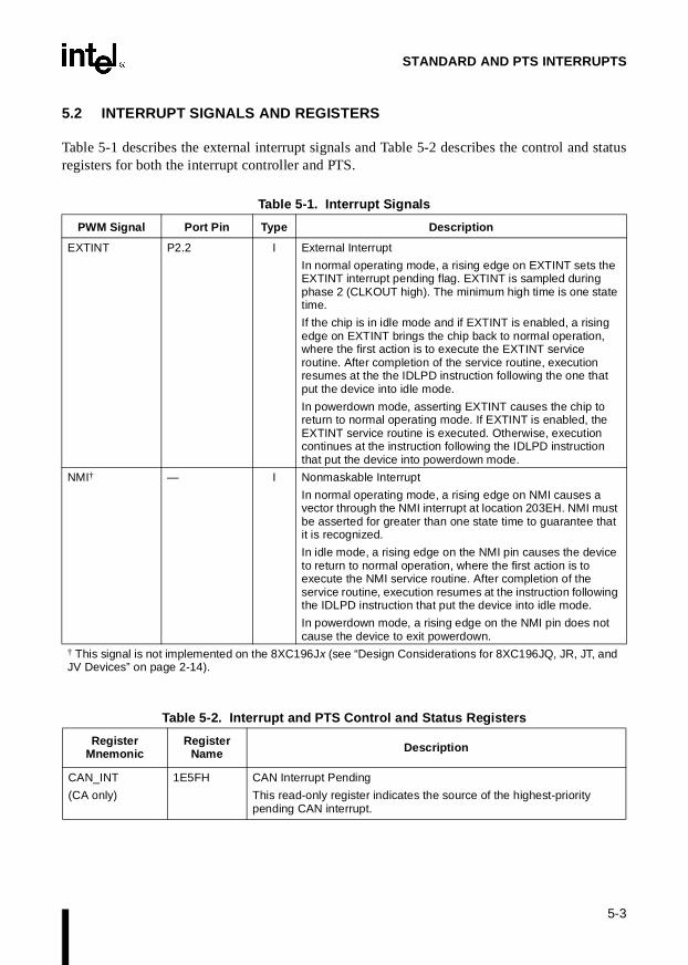
5-3
STANDARD AND PTS INTERRUPTS
5.2 INTERRUPT SIGNALS AND REGISTERS
Table 5-1 describes the external interrupt signals and Table 5-2 describes the control and statusregisters for both the interrupt controller and PTS.
Table 5-1. Interrupt Signals
PWM Signal Port Pin Type Description
EXTINT P2.2 I External Interrupt
In normal operating mode, a rising edge on EXTINT sets the EXTINT interrupt pending flag. EXTINT is sampled during phase 2 (CLKOUT high). The minimum high time is one state time.
If the chip is in idle mode and if EXTINT is enabled, a rising edge on EXTINT brings the chip back to normal operation, where the first action is to execute the EXTINT service routine. After completion of the service routine, execution resumes at the the IDLPD instruction following the one that put the device into idle mode.
In powerdown mode, asserting EXTINT causes the chip to return to normal operating mode. If EXTINT is enabled, the EXTINT service routine is executed. Otherwise, execution continues at the instruction following the IDLPD instruction that put the device into powerdown mode.
NMI† — I Nonmaskable Interrupt
In normal operating mode, a rising edge on NMI causes a vector through the NMI interrupt at location 203EH. NMI must be asserted for greater than one state time to guarantee that it is recognized.
In idle mode, a rising edge on the NMI pin causes the device to return to normal operation, where the first action is to execute the NMI service routine. After completion of the service routine, execution resumes at the instruction following the IDLPD instruction that put the device into idle mode.
In powerdown mode, a rising edge on the NMI pin does not cause the device to exit powerdown.
† This signal is not implemented on the 8XC196Jx (see “Design Considerations for 8XC196JQ, JR, JT, and JV Devices” on page 2-14).
Table 5-2. Interrupt and PTS Control and Status Registers
Register Mnemonic
Register Name Description
CAN_INT
(CA only)
1E5FH CAN Interrupt Pending
This read-only register indicates the source of the highest-priority pending CAN interrupt.
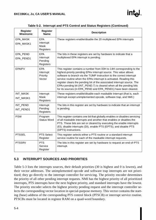
8XC196Kx, Jx, CA USER’S MANUAL
5-4
5.3 INTERRUPT SOURCES AND PRIORITIES
Table 5-3 lists the interrupts sources, their default priorities (30 is highest and 0 is lowest), andtheir vector addresses. The unimplemented opcode and software trap interrupts are not priori-tized; they go directly to the interrupt controller for servicing. The priority encoder determinesthe priority of all other pending interrupt requests. NMI has the highest priority of all prioritizedinterrupts, PTS interrupts have the next highest priority, and standard interrupts have the lowest.The priority encoder selects the highest priority pending request and the interrupt controller se-lects the corresponding vector location in special-purpose memory. This vector contains the start-ing (base) address of the corresponding PTS control block (PTSCB) or interrupt service routine.PTSCBs must be located in register RAM on a quad-word boundary.
EPA_MASK
EPA_MASK1
EPA Interrupt Mask Registers
These registers enable/disable the 20 multiplexed EPA interrupts
EPA_PEND
EPA_PEND1
EPA Interrupt Pending Registers
The bits in these registers are set by hardware to indicate that a multiplexed EPA interrupt is pending.
EPAIPV EPA Interrupt Priority Vector
This register contains a number from 00H to 14H corresponding to the highest-priority pending EPAx interrupt source. This value allows software to branch via the TIJMP instruction to the correct interrupt service routine when the EPAx interrupt is activated. Reading this register clears the pending bit of the associated interrupt source. The EPAx pending bit (INT_PEND.7) is cleared when all the pending bits for its sources (in EPA_PEND and EPA_PEND1) have been cleared.
INT_MASK
INT_MASK1
Interrupt Mask Registers
These registers enable/disable each maskable interrupt (that is, each interrupt except unimplemented opcode, software trap, and NMI.)
INT_PEND
INT_PEND1
Interrupt Pending Registers
The bits in this register are set by hardware to indicate that an interrupt is pending.
PSW Program Status Word
This register contains one bit that globally enables or disables servicing of all maskable interrupts and another that enables or disables the PTS. These bits are set or cleared by executing the enable interrupts (EI), disable interrupts (DI), enable PTS (EPTS), and disable PTS (DPTS) instructions.
PTSSEL PTS Select Register
This register selects either a PTS routine or a standard interrupt service routine for each of the maskable interrupt requests.
PTSSRV PTS Service Register
The bits in this register are set by hardware to request an end-of-PTS interrupt.
Table 5-2. Interrupt and PTS Control and Status Registers (Continued)
Register Mnemonic
Register Name Description
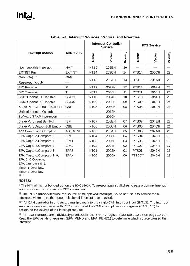
5-5
STANDARD AND PTS INTERRUPTS
Table 5-3. Interrupt Sources, Vectors, and Priorities
Interrupt Source Mnemonic
Interrupt Controller Service PTS Service
Nam
e
Vec
tor
Prio
rity
Nam
e
Vec
tor
Prio
rity
Nonmaskable Interrupt NMI† INT15 203EH 30 — — —
EXTINT Pin EXTINT INT14 203CH 14 PTS14 205CH 29
CAN (CA)†††
Reserved (Kx, Jx)
CAN
—INT13 203AH 13 PTS13†† 205AH 28
SIO Receive RI INT12 2038H 12 PTS12 2058H 27
SIO Transmit TI INT11 2036H 11 PTS11 2056H 26
SSIO Channel 1 Transfer SSIO1 INT10 2034H 10 PTS10 2054H 25
SSIO Channel 0 Transfer SSIO0 INT09 2032H 09 PTS09 2052H 24
Slave Port Command Buff Full CBF INT08 2030H 08 PTS08 2050H 23
Unimplemented Opcode — — 2012H — — — —
Software TRAP Instruction — — 2010H — — — —
Slave Port Input Buff Full IBF INT07 200EH 07 PTS07 204EH 22
Slave Port Output Buff Empty OBE INT06 200CH 06 PTS06 204CH 21
A/D Conversion Complete AD_DONE INT05 200AH 05 PTS05 204AH 20
EPA Capture/Compare 0 EPA0 INT04 2008H 04 PTS04 2048H 19
EPA Capture/Compare 1 EPA1 INT03 2006H 03 PTS03 2046H 18
EPA Capture/Compare 2 EPA2 INT02 2004H 02 PTS02 2044H 17
EPA Capture/Compare 3 EPA3 INT01 2002H 01 PTS01 2042H 16
EPA Capture/Compare 4–9, EPA 0–9 Overrun,EPA Compare 0–1, Timer 1 Overflow,Timer 2 Overflow††††
EPAx INT00 2000H 00 PTS00†† 2040H 15
NOTES:† The NMI pin is not bonded out on the 8XC196Jx. To protect against glitches, create a dummy interrupt service routine that contains a RET instruction.†† The PTS cannot determine the source of multiplexed interrupts, so do not use it to service these interrupts when more than one multiplexed interrupt is unmasked.††† All CAN-controller interrupts are multiplexed into the single CAN interrupt input (INT13). The interrupt service routine associated with INT13 must read the CAN interrupt pending register (CAN_INT) to determine the source of the interrupt request†††† These interrupts are individually prioritized in the EPAIPV register (see Table 10-16 on page 10-30). Read the EPA pending registers (EPA_PEND and EPA_PEND1) to determine which source caused the interrupt.

8XC196Kx, Jx, CA USER’S MANUAL
5-6
5.3.1 Special Interrupts
This microcontroller has three special interrupt sources that are always enabled: unimplementedopcode, software trap, and NMI. These interrupts are not affected by the EI (enable interrupts)and DI (disable interrupts) instructions, and they cannot be masked. All of these interrupts areserviced by the interrupt controller; they cannot be assigned to the PTS. Of these three, only NMIgoes through the transition detector and priority encoder. The other two special interrupts go di-rectly to the interrupt controller for servicing. Be aware that these interrupts are often assigned tospecial functions in development tools.
5.3.1.1 Unimplemented Opcode
If the CPU attempts to execute an unimplemented opcode, an indirect vector through location2012H occurs. This prevents random software execution during hardware and software failures.The interrupt vector should contain the starting address of an error routine that will not furthercorrupt an already erroneous situation. The unimplemented opcode interrupt prevents other inter-rupts from being acknowledged until after the next instruction is executed.
5.3.1.2 Software Trap
The TRAP instruction (opcode F7H) causes an interrupt call that is vectored through location2010H. The TRAP instruction provides a single-instruction interrupt that is useful when debug-ging software or generating software interrupts. The TRAP instruction prevents other interruptsfrom being acknowledged until after the next instruction is executed.
5.3.1.3 NMI
The external NMI pin generates a nonmaskable interrupt for implementation of critical interruptroutines. NMI has the highest priority of all the prioritized interrupts. It is passed directly fromthe transition detector to the priority encoder, and it vectors indirectly through location 203EH.(The NMI pin is not implemented on the 8XC196Jx. To protect against glitches, create a dummyinterrupt service routine that contains a RET instruction.) The NMI pin is sampled during phase2 (CLKOUT high) and is latched internally. Because interrupts are edge-triggered, only one in-terrupt is generated, even if the pin is held high. If your system does not use the NMI interrupt,connect the NMI pin to VSS to prevent spurious interrupts.
5.3.2 External Interrupt Pins
The interrupt detection logic can generate an interrupt if a momentary negative glitch occurswhile the input pin is held high. For this reason, interrupt inputs should normally be held lowwhen they are inactive.

5-7
STANDARD AND PTS INTERRUPTS
5.3.3 Multiplexed Interrupt Sources
Both the EPAx and CAN (CA only) interrupts are generated by a group of multiplexed interruptsources. The EPA4–9 and COMP0–1 event interrupts, the EPA0–9 overrun interrupts, and thetimer 1 and timer 2 overflow/underflow interrupts are multiplexed into EPAx. All CAN-controllerinterrupts are multiplexed into the single CAN interrupt. Generally, PTS interrupt service is notuseful for multiplexed interrupts because the PTS cannot readily determine the interrupt source.Your interrupt service routine should read the EPA_PEND or EPA_PEND1 register (EPAx) or theCAN_INT (CAN) regsiter to determine the source of the interrupt and to ensure that no additionalinterrupts are pending before executing the return instruction. Chapter 10, “Event Processor Ar-ray (EPA)” and Chapter 12, “CAN Serial Communications Controller” discuss the EPA and CANinterrupts in detail.
5.3.4 End-of-PTS Interrupts
When the PTSCOUNT register decrements to zero at the end of a single transfer, block transfer,or A/D scan routine, hardware clears the corresponding bit in the PTSSEL register, which disablesPTS service for that interrupt. It also sets the corresponding PTSSRV bit, requesting an end-of-PTS interrupt. An end-of-PTS interrupt has the same priority as a corresponding standard inter-rupt. The interrupt controller processes it with an interrupt service routine that is stored in thememory location pointed to by the standard interrupt vector. For example, the PTS services theSIO transmit interrupt if PTSSEL.11 is set. The interrupt vectors through 2056H, but the corre-sponding end-of-PTS interrupt vectors through 2036H, the standard SIO transmit interrupt vector.When the end-of-PTS interrupt vectors to the interrupt service routine, hardware clears the PTSS-RV bit. The end-of-PTS interrupt service routine should reinitialize the PTSCB, if required, andset the appropriate PTSSEL bit to re-enable PTS interrupt service.
5.4 INTERRUPT LATENCY
Interrupt latency is the total delay between the time that the interrupt request is generated (notacknowledged) and the time that the device begins executing either the standard interrupt serviceroutine or the PTS interrupt service routine. A delay occurs between the time that the interruptrequest is detected and the time that it is acknowledged. An interrupt request is acknowledgedwhen the current instruction finishes executing. If the interrupt request occurs during one of thelast four state times of the instruction, it may not be acknowledged until after the next instructionfinishes. This additional delay occurs because instructions are prefetched and prepared a few statetimes before they are executed. Thus, the maximum delay between interrupt request and ac-knowledgment is four state times plus the execution time of the next instruction.
8XC196Kx, Jx, CA USER’S MANUAL
5-8
When a standard interrupt request is acknowledged, the hardware clears the interrupt pending bitand forces a call to the address contained in the corresponding interrupt vector after completingthe current instruction. The procedure that gets the vector and forces the call requires 11 statetimes. If the stack is in external RAM, the call requires an additional two state times assuming azero-wait-state bus.
When a PTS interrupt request is acknowledged, it immediately vectors to the PTSCB and beginsexecuting the PTS routine.
5.4.1 Situations that Increase Interrupt Latency
If an interrupt request occurs while any of the following instructions are executing, the interruptwill not be acknowledged until after the next instruction is executed:
• the signed prefix opcode (FE) for the two-byte, signed multiply and divide instructions
• any of these eight protected instructions: DI, EI, DPTS, EPTS, POPA, POPF, PUSHA,PUSHF (see Appendix A for descriptions of these instructions)
• any of the read-modify-write instructions: AND, ANDB, OR, ORB, XOR, XORB
Both the unimplemented opcode interrupt and the software trap interrupt prevent other interruptrequests from being acknowledged until after the next instruction is executed.
Each PTS cycle within a PTS routine cannot be interrupted. A PTS cycle is the entire PTS re-sponse to a single interrupt request. In block transfer mode, a PTS cycle consists of the transferof an entire block of bytes or words. This means a worst-case latency of 500 states if you assumea block transfer of 32 words from one external memory location to another. See Table 5-4 on page5-10 for PTS cycle execution times.
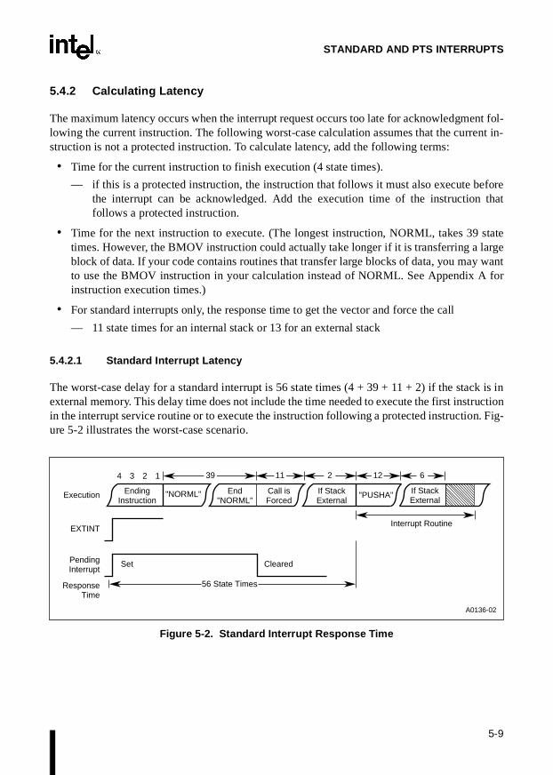
5-9
STANDARD AND PTS INTERRUPTS
5.4.2 Calculating Latency
The maximum latency occurs when the interrupt request occurs too late for acknowledgment fol-lowing the current instruction. The following worst-case calculation assumes that the current in-struction is not a protected instruction. To calculate latency, add the following terms:
• Time for the current instruction to finish execution (4 state times).
— if this is a protected instruction, the instruction that follows it must also execute beforethe interrupt can be acknowledged. Add the execution time of the instruction thatfollows a protected instruction.
• Time for the next instruction to execute. (The longest instruction, NORML, takes 39 statetimes. However, the BMOV instruction could actually take longer if it is transferring a largeblock of data. If your code contains routines that transfer large blocks of data, you may wantto use the BMOV instruction in your calculation instead of NORML. See Appendix A forinstruction execution times.)
• For standard interrupts only, the response time to get the vector and force the call
— 11 state times for an internal stack or 13 for an external stack
5.4.2.1 Standard Interrupt Latency
The worst-case delay for a standard interrupt is 56 state times (4 + 39 + 11 + 2) if the stack is inexternal memory. This delay time does not include the time needed to execute the first instructionin the interrupt service routine or to execute the instruction following a protected instruction. Fig-ure 5-2 illustrates the worst-case scenario.
Figure 5-2. Standard Interr upt Response Time
A0136-02
11 2 1239
Ending Instruction
End "NORML"
Call is Forced
If Stack External
"PUSHA"
Interrupt Routine
ClearedSet
Execution
EXTINT
Pending Interrupt
Response Time
56 State Times
If Stack External
6
"NORML"
4 3 2 1

8XC196Kx, Jx, CA USER’S MANUAL
5-10
5.4.2.2 PTS Interrupt Latency
The maximum delay for a PTS interrupt is 43 state times (4 + 39). This delay time does not in-clude the added delay if a protected instruction is being executed or if a PTS request is already inprogress. See Table 5-4 for execution times for PTS routines.
Figure 5-3. PTS Interrupt Res ponse Time
Table 5-4. Execution Times for PTS Cycles
PTS Mode Execution Time (in State Times)
Single transfer moderegister/register†
memory/register†memory/memory†
18 per byte or word transfer + 1 21 per byte or word transfer + 1 24 per byte or word transfer + 1
Block transfer moderegister/register†
memory/register†memory/memory†
13 + 7 per byte or word transfer (1 minimum)16 + 7 per byte or word transfer (1 minimum)19 + 7 per byte or word transfer (1 minimum)
A/D scan moderegister/register†
register/memory†2125
PWM remap mode 15
PWM toggle mode 15
† Register indicates an access to the register file or peripheral SFR. Memory indicates an access to a memory-mapped register, I/O, or memory. See Table 4-1 on page 4-2 for address information.
Ending Instruction
End "NORML"
Vector to PTS Control Block
PTS
PTS Interrupt Routine
ClearedSet
Execution
EXTINT
Pending Interrupt
Response TimeLatency Time
"NORML"
43 State Times
PTS
A0142-01
4 3 2 1 39

5-11
STANDARD AND PTS INTERRUPTS
5.5 PROGRAMMING THE INTERRUPTS
The PTS select register (PTSSEL) selects either PTS service or a standard software interrupt ser-vice routine for each of the maskable interrupt requests (see Figure 5-4). The interrupt mask reg-isters, INT_MASK and INT_MASK1, enable or disable (mask) individual interrupts (see Figures5-5 and 5-6). With the exception of the nonmaskable interrupt (NMI) bit (INT_MASK1.7), set-ting a bit enables the corresponding interrupt source and clearing a bit disables the source.
To disable any interrupt, clear its mask bit. To enable an interrupt for standard interrupt service,set its mask bit and clear its PTS select bit. To enable an interrupt for PTS service, set both themask bit and the PTS select bit.
Additionally, when you assign an interrupt to the PTS, you must set up a PTS control block(PTSCB) for each interrupt source (see “Initializing the PTS Control Blocks” on page 5-18) anduse the EPTS instruction to globally enable the PTS. When you assign an interrupt to a standardsoftware service routine, use the EI (enable interrupts) instruction to globally enable interrupt ser-vicing.
NOTE
PTS routines will execute after a DI (disable interrupts) instruction, if the appropriate INT_MASK and PTSSEL bits are set. However, the end-of-PTS interrupt request will not occur. If an interrupt request occurs while interrupts are disabled, the corresponding pending bit is set in the INT_PEND or INT_PEND1 register.
5.5.1 Programming the Multiplexed Interrupts
On the 87C196CA, the CAN-controller interrupts are multiplexed into the single CAN interruptinput (INT13). Write to the CAN control register (Figure 12-6 on page 12-13) to enable or disableglobal CAN interrupt sources (error, status change, and individual message object) andINT_MASK1.5 to enable or disable the multiplexed CAN interrupt.
The EPA4–9 and COMP0–1 event interrupts, the EPA0–9 overrun interrupts, and the timer 1 andtimer 2 overflow/underflow interrupts are multiplexed into EPAx. Write to the EPA_MASK (Fig-ure 10-12 on page 10-27) or EPA_MASK1 (Figure 10-13 on page 10-27) registers to enable ordisable the multiplexed EPA interrupt sources and INT_MASK.0 to enable or disable the EPAxinterrupt.
The PTS cannot determine the source of multiplexed interrupts, so do not use it to service theseinterrupts when more than one multiplexed interrupt is unmasked.

8XC196Kx, Jx, CA USER’S MANUAL
5-12
PTSSEL Address:Reset State:
04H0000H
The PTS select (PTSSEL) register selects either a PTS microcode routine or a standard interrupt service routine for each interrupt requests. Setting a bit selects a PTS microcode routine; clearing a bit selects a standard interrupt service routine. When PTSCOUNT reaches zero, hardware clears the corresponding PTSSEL bit. The PTSSEL bit must be set manually to re-enable the PTS channel.
15 8
87C196CA — EXTINT CAN RI TI SSIO1 SSIO0 —
7 0
— — AD EPA0 EPA1 EPA2 EPA3 EPAx
15 8
8XC196Jx — EXTINT — RI TI SSIO1 SSIO0 —
7 0
— — AD EPA0 EPA1 EPA2 EPA3 EPAx
15 8
8XC196Kx — EXTINT — RI TI SSIO1 SSIO0 CBF
7 0
IBF OBE AD EPA0 EPA1 EPA2 EPA3 EPAx
BitNumber Function
14:0(Note 1)
Setting this bit causes the corresponding interrupt to be handled by a PTS microcode routine.
The PTS interrupt vector locations are as follows:
Bit Mnemonic Interrupt PTS VectorEXTINT EXTINT pin 205CHCAN (CA)† CAN Peripheral 205AHRI SIO Receive 2058HTI SIO Transmit 2056HSSIO1 SSIO 1 Transfer 2054HSSIO0 SSIO 0 Transfer 2052HCBF (Kx) Slave Port Command Buffer Full 2050HIBF (Kx) Slave Port Input Buffer Full 204EHOBE (Kx) Slave Port Output Buffer Empty 204CHAD A/D Conversion Complete 204AHEPA0 EPA Capture/Compare Channel 0 2048HEPA1 EPA Capture/Compare Channel 1 2046HEPA2 EPA Capture/Compare Channel 2 2044HEPA3 EPA Capture/Compare Channel 3 2042HEPAx† Multiplexed EPA 2040H
† PTS service is not recommended because the PTS cannot determine the source of multiplexed interrupts.
1. Bit 13 is reserved on the 8XC196Jx, Kx devices and bits 6–8 are reserved on the 87C196CA,8XC196Jx devices. For compatibility with future devices, write zeros to these bits.
Figure 5-4. PTS Select (PTSSEL) Register
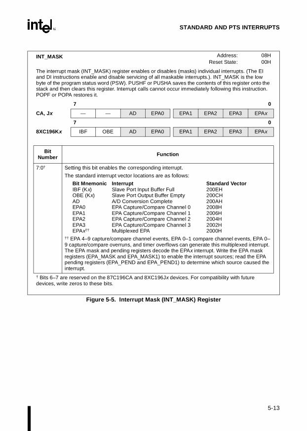
5-13
STANDARD AND PTS INTERRUPTS
INT_MASK Address:Reset State:
08H00H
The interrupt mask (INT_MASK) register enables or disables (masks) individual interrupts. (The EI and DI instructions enable and disable servicing of all maskable interrupts.). INT_MASK is the low byte of the program status word (PSW). PUSHF or PUSHA saves the contents of this register onto the stack and then clears this register. Interrupt calls cannot occur immediately following this instruction. POPF or POPA restores it.
7 0
CA, Jx — — AD EPA0 EPA1 EPA2 EPA3 EPAx
7 0
8XC196Kx IBF OBE AD EPA0 EPA1 EPA2 EPA3 EPAx
BitNumber Function
7:0† Setting this bit enables the corresponding interrupt.
The standard interrupt vector locations are as follows:
Bit Mnemonic Interrupt Standard VectorIBF (Kx) Slave Port Input Buffer Full 200EHOBE (Kx) Slave Port Output Buffer Empty 200CHAD A/D Conversion Complete 200AHEPA0 EPA Capture/Compare Channel 0 2008HEPA1 EPA Capture/Compare Channel 1 2006HEPA2 EPA Capture/Compare Channel 2 2004HEPA3 EPA Capture/Compare Channel 3 2002HEPAx†† Multiplexed EPA 2000H
†† EPA 4–9 capture/compare channel events, EPA 0–1 compare channel events, EPA 0–9 capture/compare overruns, and timer overflows can generate this multiplexed interrupt. The EPA mask and pending registers decode the EPAx interrupt. Write the EPA mask registers (EPA_MASK and EPA_MASK1) to enable the interrupt sources; read the EPA pending registers (EPA_PEND and EPA_PEND1) to determine which source caused the interrupt.
† Bits 6–7 are reserved on the 87C196CA and 8XC196Jx devices. For compatibility with future devices, write zeros to these bits.
Figure 5-5. Interrupt Mask (INT_M ASK) Register
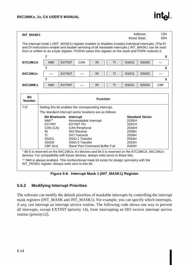
8XC196Kx, Jx, CA USER’S MANUAL
5-14
5.5.2 Modifying Interrupt Priorities
The software can modify the default priorities of maskable interrupts by controlling the interruptmask registers (INT_MASK and INT_MASK1). For example, you can specify which interrupts,if any, can interrupt an interrupt service routine. The following code shows one way to preventall interrupts, except EXTINT (priority 14), from interrupting an SIO receive interrupt serviceroutine (priority12).
INT_MASK1 Address:Reset State:
13H00H
The interrupt mask 1 (INT_MASK1) register enables or disables (masks) individual interrupts. (The EI and DI instructions enable and disable servicing of all maskable interrupts.) INT_MASK1 can be read from or written to as a byte register. PUSHA saves this register on the stack and POPA restores it.
7 0
87C196CA NMI EXTINT CAN RI TI SSIO1 SSIO0 —
7 0
8XC196Jx — EXTINT — RI TI SSIO1 SSIO0 —
7 0
8XC196Kx NMI EXTINT — RI TI SSIO1 SSIO0 CBF
BitNumber Function
7:0† Setting this bit enables the corresponding interrupt.
The standard interrupt vector locations are as follows:
Bit Mnemonic Interrupt Standard VectorNMI†† Nonmaskable Interrupt 203EHEXTINT EXTINT Pin 203CHCAN (CA) CAN Peripheral 203AHRI SIO Receive 2038HTI SIO Transmit 2036HSSIO1 SSIO 1 Transfer 2034HSSIO0 SSIO 0 Transfer 2032HCBF (Kx) Slave Port Command Buffer Full 2030H
† Bit 5 is reserved on the 8XC196Jx, Kx devices and bit 0 is reserved on the 87C196CA, 8XC196Jx devices. For compatibility with future devices, always write zeros to these bits.†† NMI is always enabled. This nonfunctional mask bit exists for design symmetry with the INT_PEND1 register. Always write zero to this bit.
Figure 5-6. Interrupt Mask 1 (INT_MASK1) Regi ster
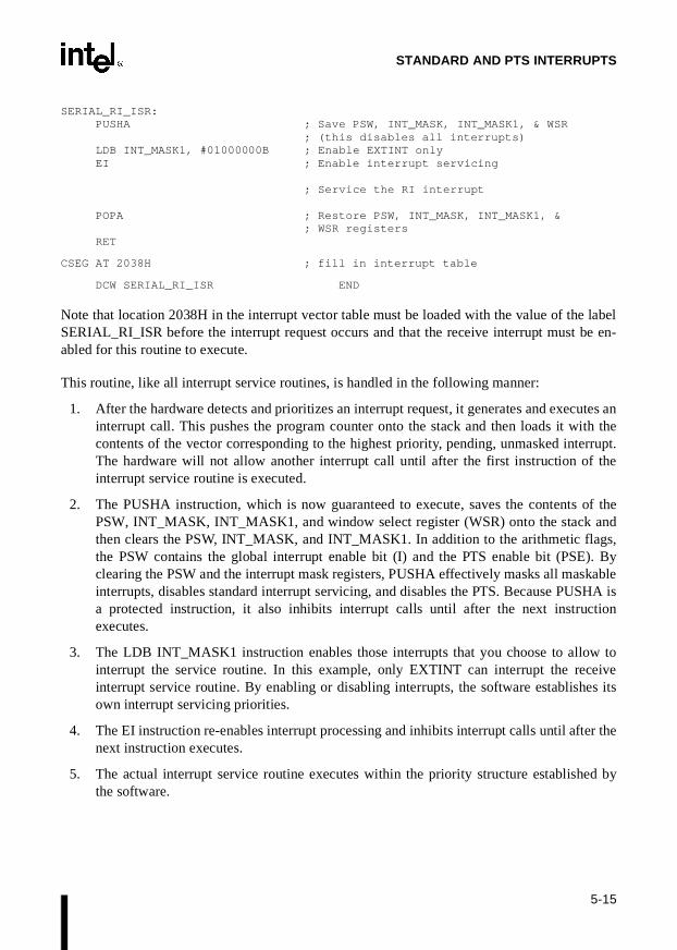
5-15
STANDARD AND PTS INTERRUPTS
SERIAL_RI_ISR: PUSHA ; Save PSW, INT_MASK, INT_MASK1, & WSR
; (this disables all interrupts) LDB INT_MASK1, #01000000B ; Enable EXTINT onlyEI ; Enable interrupt servicing
; Service the RI interrupt
POPA ; Restore PSW, INT_MASK, INT_MASK1, & ; WSR registers
RET
CSEG AT 2038H ; fill in interrupt table
DCW SERIAL_RI_ISR END
Note that location 2038H in the interrupt vector table must be loaded with the value of the labelSERIAL_RI_ISR before the interrupt request occurs and that the receive interrupt must be en-abled for this routine to execute.
This routine, like all interrupt service routines, is handled in the following manner:
1. After the hardware detects and prioritizes an interrupt request, it generates and executes aninterrupt call. This pushes the program counter onto the stack and then loads it with thecontents of the vector corresponding to the highest priority, pending, unmasked interrupt.The hardware will not allow another interrupt call until after the first instruction of theinterrupt service routine is executed.
2. The PUSHA instruction, which is now guaranteed to execute, saves the contents of thePSW, INT_MASK, INT_MASK1, and window select register (WSR) onto the stack andthen clears the PSW, INT_MASK, and INT_MASK1. In addition to the arithmetic flags,the PSW contains the global interrupt enable bit (I) and the PTS enable bit (PSE). Byclearing the PSW and the interrupt mask registers, PUSHA effectively masks all maskableinterrupts, disables standard interrupt servicing, and disables the PTS. Because PUSHA isa protected instruction, it also inhibits interrupt calls until after the next instructionexecutes.
3. The LDB INT_MASK1 instruction enables those interrupts that you choose to allow tointerrupt the service routine. In this example, only EXTINT can interrupt the receiveinterrupt service routine. By enabling or disabling interrupts, the software establishes itsown interrupt servicing priorities.
4. The EI instruction re-enables interrupt processing and inhibits interrupt calls until after thenext instruction executes.
5. The actual interrupt service routine executes within the priority structure established bythe software.

8XC196Kx, Jx, CA USER’S MANUAL
5-16
6. At the end of the service routine, the POPA instruction restores the original contents of thePSW, INT_MASK, INT_MASK1, and WSR registers; any changes made to theseregisters during the interrupt service routine are overwritten. Because interrupt callscannot occur immediately following a POPA instruction, the last instruction (RET) willexecute before another interrupt call can occur.
Notice that the “preamble” and exit code for this routine does not save or restore register RAM.The interrupt service routine is assumed to allocate its own private set of registers from the lowerregister file. The general-purpose register RAM in the lower register file makes this quite practi-cal. In addition, the RAM in the upper register file is available via windowing (see “Windowing”on page 4-13).
5.5.3 Determining the Source of an Interrupt
When the transition detector detects an interrupt, it sets the corresponding bit in the INT_PENDor INT_PEND1 register (Figures 5-7 and 5-8). This bit is set even if the individual interrupt isdisabled (masked). The pending bit is cleared when the program vectors to the interrupt serviceroutine. INT_PEND and INT_PEND1 can be read, to determine which interrupts are pending.They can also be modified (written), either to clear pending interrupts or to generate interruptsunder software control. However, we recommend the use of the read-modify-write instructions,such as AND and OR, to modify these registers.
ANDB INT_PEND, #11111110B ; Clears the EPA x interrupt ORB INT_PEND, #00000001B ; Sets the EPA x interrupt
Other methods could result in a partial interrupt cycle. For example, an interrupt could occur dur-ing an instruction sequence that loads the contents of the interrupt pending register into a tempo-rary register, modifies the contents of the temporary register, and then writes the contents of thetemporary register back into the interrupt pending register. If the interrupt occurs during one ofthe last four states of the second instruction, it will not be acknowledged until after the completionof the third instruction. The third instruction overwrites the contents of the interrupt pending reg-ister, so the jump to the interrupt vector will not occur.
5.5.3.1 Determining the Source of Multiplexed Interrupts
On the 87C196CA, the CAN-controller interrupts are multiplexed into the single CAN interruptinput (INT13). The interrupt service routine associated with INT13 must read the CAN interruptpending register (CAN_INT, Figure 12-19 on page 12-32) to determine the source of the interruptrequest.
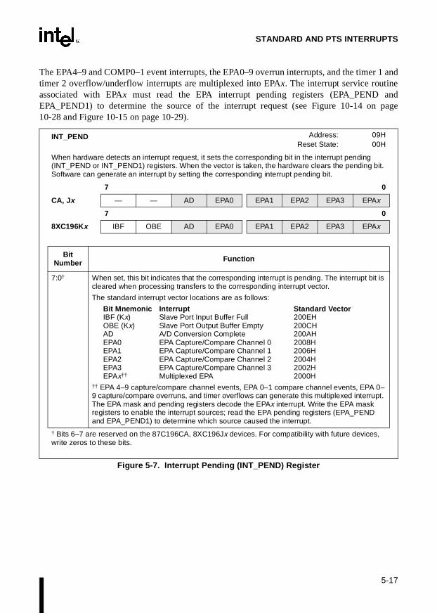
5-17
STANDARD AND PTS INTERRUPTS
The EPA4–9 and COMP0–1 event interrupts, the EPA0–9 overrun interrupts, and the timer 1 andtimer 2 overflow/underflow interrupts are multiplexed into EPAx. The interrupt service routineassociated with EPAx must read the EPA interrupt pending registers (EPA_PEND andEPA_PEND1) to determine the source of the interrupt request (see Figure 10-14 on page10-28 and Figure 10-15 on page 10-29).
INT_PEND Address:Reset State:
09H00H
When hardware detects an interrupt request, it sets the corresponding bit in the interrupt pending (INT_PEND or INT_PEND1) registers. When the vector is taken, the hardware clears the pending bit. Software can generate an interrupt by setting the corresponding interrupt pending bit.
7 0
CA, Jx — — AD EPA0 EPA1 EPA2 EPA3 EPAx
7 0
8XC196Kx IBF OBE AD EPA0 EPA1 EPA2 EPA3 EPAx
BitNumber Function
7:0† When set, this bit indicates that the corresponding interrupt is pending. The interrupt bit is cleared when processing transfers to the corresponding interrupt vector.
The standard interrupt vector locations are as follows:
Bit Mnemonic Interrupt Standard VectorIBF (Kx) Slave Port Input Buffer Full 200EHOBE (Kx) Slave Port Output Buffer Empty 200CHAD A/D Conversion Complete 200AHEPA0 EPA Capture/Compare Channel 0 2008HEPA1 EPA Capture/Compare Channel 1 2006HEPA2 EPA Capture/Compare Channel 2 2004HEPA3 EPA Capture/Compare Channel 3 2002HEPAx†† Multiplexed EPA 2000H
†† EPA 4–9 capture/compare channel events, EPA 0–1 compare channel events, EPA 0–9 capture/compare overruns, and timer overflows can generate this multiplexed interrupt. The EPA mask and pending registers decode the EPAx interrupt. Write the EPA mask registers to enable the interrupt sources; read the EPA pending registers (EPA_PEND and EPA_PEND1) to determine which source caused the interrupt.
† Bits 6–7 are reserved on the 87C196CA, 8XC196Jx devices. For compatibility with future devices, write zeros to these bits.
Figure 5-7. Interrupt Pending (INT_PEND) Register

8XC196Kx, Jx, CA USER’S MANUAL
5-18
5.6 INITIALIZING THE PTS CONTROL BLOCKS
Each PTS interrupt requires a block of data called the PTS control block (PTSCB). The PTSCBidentifies which PTS microcode routine will be invoked and sets up the specific parameters forthe routine. You must set up the PTSCB for each interrupt source before enabling the correspond-ing PTS interrupts.
INT_PEND1 Address:Reset State:
12H00H
When hardware detects a pending interrupt, it sets the corresponding bit in the interrupt pending (INT_PEND or INT_PEND1) registers. When the vector is taken, the hardware clears the pending bit. Software can generate an interrupt by setting the corresponding interrupt pending bit.
7 8
87C196CA NMI EXTINT CAN RI TI SSIO1 SSIO0 —
7 0
8XC196Jx — EXTINT — RI I TI SSIO1 SSIO0 —
7 0
8XC196Kx NMI EXTINT — RI I TI SSIO1 SSIO0 CBF
BitNumber Function
7:0† When set, this bit indicates that the corresponding interrupt is pending. The interrupt bit is cleared when processing transfers to the corresponding interrupt vector.
The standard interrupt vector locations are as follows:
Bit Mnemonic Interrupt Standard VectorNMI Nonmaskable Interrupt 203EHEXTINT EXTINT Pin 203CHCAN (CA)†† CAN Peripheral 203AHRI SIO Receive 2038HTI SIO Transmit 2036HSSIO1 SSIO 1 Transfer 2034HSSIO0 SSIO 0 Transfer 2032HCBF (Kx) Slave Port Command Buffer Full 2030H
†† All CAN-controller interrupts are multiplexed into the single CAN interrupt input (INT13). The interrupt service routine associated with INT13 must read the CAN interrupt pending register (CAN_INT) to determine the source of the interrupt request.
† Bit 7 is reserved on the 8XC196Jx devices, bit 5 is reserved on the 8XC196Jx, Kx devices, and bit 0 is reserved on the 87C196CA, 8XC196Jx devices. For compatibility with future devices, always write zeros to these bits.
Figure 5-8. Interrupt Pending 1 (INT_PEND1) Register
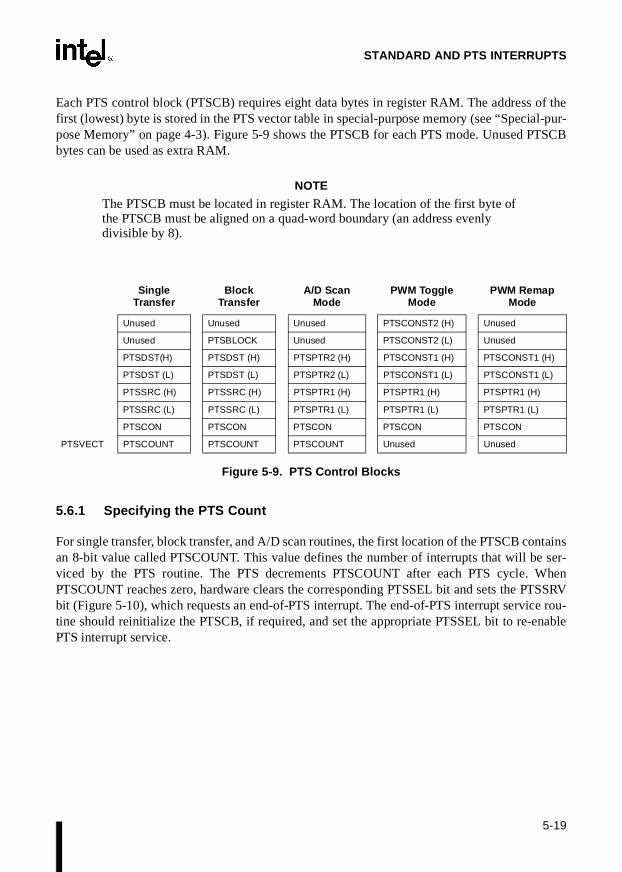
5-19
STANDARD AND PTS INTERRUPTS
Each PTS control block (PTSCB) requires eight data bytes in register RAM. The address of thefirst (lowest) byte is stored in the PTS vector table in special-purpose memory (see “Special-pur-pose Memory” on page 4-3). Figure 5-9 shows the PTSCB for each PTS mode. Unused PTSCBbytes can be used as extra RAM.
NOTE
The PTSCB must be located in register RAM. The location of the first byte of the PTSCB must be aligned on a quad-word boundary (an address evenly divisible by 8).
Figure 5-9. PTS Cont rol Blocks
5.6.1 Specifying the PTS Count
For single transfer, block transfer, and A/D scan routines, the first location of the PTSCB containsan 8-bit value called PTSCOUNT. This value defines the number of interrupts that will be ser-viced by the PTS routine. The PTS decrements PTSCOUNT after each PTS cycle. WhenPTSCOUNT reaches zero, hardware clears the corresponding PTSSEL bit and sets the PTSSRVbit (Figure 5-10), which requests an end-of-PTS interrupt. The end-of-PTS interrupt service rou-tine should reinitialize the PTSCB, if required, and set the appropriate PTSSEL bit to re-enablePTS interrupt service.
Single Transfer
Block Transfer
A/D Scan Mode
PWM Toggle Mode
PWM Remap Mode
Unused Unused Unused PTSCONST2 (H) Unused
Unused PTSBLOCK Unused PTSCONST2 (L) Unused
PTSDST(H) PTSDST (H) PTSPTR2 (H) PTSCONST1 (H) PTSCONST1 (H)
PTSDST (L) PTSDST (L) PTSPTR2 (L) PTSCONST1 (L) PTSCONST1 (L)
PTSSRC (H) PTSSRC (H) PTSPTR1 (H) PTSPTR1 (H) PTSPTR1 (H)
PTSSRC (L) PTSSRC (L) PTSPTR1 (L) PTSPTR1 (L) PTSPTR1 (L)
PTSCON PTSCON PTSCON PTSCON PTSCON
PTSVECT PTSCOUNT PTSCOUNT PTSCOUNT Unused Unused

8XC196Kx, Jx, CA USER’S MANUAL
5-20
PTSSRV Address:Reset State:
06H0000H
The PTS service (PTSSRV) register is used by the hardware to indicate that the final PTS interrupt has been serviced by the PTS routine. When PTSCOUNT reaches zero, hardware clears the corre-sponding PTSSEL bit and sets the PTSSRV bit, which requests the end-of-PTS interrupt. When the end-of-PTS interrupt is called, hardware clears the PTSSRV bit. The PTSSEL bit must be set manually to re-enable the PTS channel.
15 8
87C196CA — EXTINT CAN RI TI SSIO1 SSIO0 —
7 0
— — AD EPA0 EPA1 EPA2 EPA3 EPAx
15 8
8XC196Jx — EXTINT — RI TI SSIO1 SSIO0 —
7 0
— — AD EPA0 EPA1 EPA2 EPA3 EPAx
15 8
8XC196Kx — EXTINT — RI TI SSIO1 SSIO0 CBF
7 0
IBF OBE AD EPA0 EPA1 EPA2 EPA3 EPAx
BitNumber Function
14:0(Note 1)
This bit is set by hardware to request an end-of-PTS interrupt for the corresponding interrupt through its standard interrupt vector.
The standard interrupt vector locations are as follows.
Bit Mnemonic Interrupt Standard VectorEXTINT External 203CHCAN (CA) CAN Peripheral 203AHRI SIO Receive 2038HTI SIO Transmit 2036HSSIO1 SSIO1 Transfer 2034HSSIO0 SSIO0 Transfer 2032HCBF (Kx) Slave Port Command Buffer Full 2030HIBF (Kx Slave Port Input Buffer Full 200EHOBE (Kx) Slave Port Output Buffer Empty 200CHAD A/D Conversion Complete 200AHEPA0 EPA Capture/Compare Channel 0 2008HEPA1 EPA Capture/Compare Channel 1 2006HEPA2 EPA Capture/Compare Channel 2 2004HEPA3 EPA Capture/Compare Channel 3 2002HEPAx† Multiplexed EPA 2000H
† This bit is cleared when all EPA interrupt pending bits (EPA_PEND and EPA_PEND1) are cleared.
1. Bit 13 is reserved on the 8XC196Jx, Kx devices and bits 6–8 are reserved on the 87C196CA,8XC196Jx devices. For compatibility with future devices, write zeros to these bits.
Figure 5-10. PTS Service (PTSSRV) Register

5-21
STANDARD AND PTS INTERRUPTS
5.6.2 Selecting the PTS Mode
The second byte of each PTSCB is always an 8-bit value called PTSCON. Bits 5–7 select the PTSmode (Figure 5-11). The function of bits 0–4 differ for each PTS mode. Refer to the sections thatdescribe each routine in detail to see the function of these bits. Table 5-4 on page 5-10 lists theexecution times for each PTS mode.
5.6.3 Single Transfer Mode
In single transfer mode, an interrupt causes the PTS to transfer a single byte or word (selected bythe BW bit in PTSCON) from one memory location to another. This mode is typically used withserial I/O, or synchronous serial I/O, or slave port interrupts. It can also be used with the EPA tomove captured time values from the event-time register to internal RAM for further processing.See AP-445, 8XC196KR Peripherals: A User’s Point of View, for application examples with code.Figure 5-12 shows the PTS control block for single transfer mode.
PTSCON Address: PTSPCB + 1
The PTS control (PTSCON) register selects the PTS mode and sets up control functions for that mode.
7 0
M2 M1 M0 † † † † †
Bit Number
Bit Mnemonic Function
7:5 M2:0 PTS Mode
These bits select the PTS mode:
M2 M1 M00 0 0 block transfer0 0 1 reserved0 1 0 PWM toggle or remap0 1 1 reserved1 0 0 single transfer1 0 1 reserved1 1 0 A/D scan1 1 1 reserved
† The function of this bit depends upon which mode is selected. See the PTS control block description in each PTS mode section.
Figure 5-11. PTS Mode Selection Bits (PTSCON Bits 7:5)

8XC196Kx, Jx, CA USER’S MANUAL
5-22
PTS Single Transfer Mode Control Block
In single transfer mode, the PTS control block contains a source and destination address (PTSSRC and PTSDST), a control register (PTSCON), and a transfer count (PTSCOUNT).
7 0
Unused 0 0 0 0 0 0 0 0
7 0
Unused 0 0 0 0 0 0 0 0
15 8
PTSDST (HI) PTS Destination Address (high byte)
7 0
PTSDST (LO) PTS Destination Address (low byte)
15 8
PTSSRC (HI) PTS Source Address (high byte)
7 0
PTSSRC (LO) PTS Source Address (low byte)
7 0
PTSCON M2 M1 M0 BW SU DU SI DI
7 0
PTSCOUNT Consecutive Byte or Word Transfers
Register Location Function
PTSDST PTSCB + 4 PTS Destination Address
Write the destination memory location to this register. A valid address is any unreserved memory location; however, it must point to an even address if word transfers are selected.
PTSSRC PTSCB + 2 PTS Source Address
Write the source memory location to this register. A valid address is any unreserved memory location; however, it must point to an even address if word transfers are selected.
Figure 5-12. PTS Control Block – Single Transfer Mode

5-23
STANDARD AND PTS INTERRUPTS
The PTSCB in Table 5-5 defines nine PTS cycles. Each cycle moves a single word from location20H to an external memory location. The PTS transfers the first word to location 6000H. Then itincrements and updates the destination address and decrements the PTSCOUNT register; it doesnot increment the source address. When the second cycle begins, the PTS moves a second wordfrom location 20H to location 6002H. When PTSCOUNT equals zero, the PTS will have filledlocations 6000H–600FH, and an end-of-PTS interrupt is generated.
Register Location Function
PTSCON PTSCB + 1 PTS Control Bits
M2:0 PTS Mode
M2 M1 M01 0 0 single transfer mode
BW Byte/Word Transfer
0 = word transfer1 = byte transfer
SU† Update PTSSRC
0 = reload original PTS source address after each byte or word transfer
1 = retain current PTS source address after each byte or word transfer
DU† Update PTSDST
0 = reload original PTS destination address after each byte or word transfer
1 = retain current PTS destination address after each byte or word transfer
SI† PTSSRC Autoincrement
0 = do not increment the contents of PTSSRC1 = increment the contents of PTSSRC after each byte or word
transfer
DI† PTSDST Autoincrement
0 = do not increment the contents of PTSDST1 = increment the contents of PTSDST after each byte or word
transfer
PTSCOUNT PTSCB + 0 Consecutive Word or Byte Transfers
Defines the number of words or bytes that will be transferred during the single transfer routine. Each word or byte transfer is one PTS cycle. Maximum value is 255.
† In single transfer mode, the DU and SU bits and DI and SI bits are paired. Each pair must be set or cleared together. However, the two pairs, DU/SU and DI/SI, need not be equal.
PTS Single Transfer Mode Control Block (Continued)
Figure 5-12. PTS Control Block – Single Transfer Mode (Continued)

8XC196Kx, Jx, CA USER’S MANUAL
5-24
5.6.4 Block Transfer Mode
In block transfer mode, an interrupt causes the PTS to move a block of bytes or words from onememory location to another. See AP-445, 8XC196KR Peripherals: A User’s Point of View, for ap-plication examples with code. Figure 5-12 shows the PTS control block for block transfer modes.
In this mode, each PTS cycle consists of the transfer of an entire block of bytes or words. Becausea PTS cycle cannot be interrupted, the block transfer mode can create long interrupt latency. Theworst-case latency could be as high as 500 states, if you assume a block transfer of 32 words fromone external memory location to another, using an 8-bit bus with no wait states. See Table 5-4 onpage 5-10 for execution times of PTS routines.
The PTSCB in Table 5-6 sets up three PTS cycles that will transfer five bytes from memory loca-tions 20H–24H to 6000H–6004H (cycle 1), 6005H–6009H (cycle 2), and 600AH–600EH (cycle3). The source and destination are incremented after each byte transfer, but the original sourceaddress is reloaded into PTSSRC at the end of each block-transfer cycle. In this routine, the PTSalways gets the first byte from location 20H.
Table 5-5. Single Transfer Mode PTSCBUnused
Unused
PTSDST (HI) = 60H
PTSDST (LO) = 00H
PTSSRC (HI) = 00H
PTSSRC (LO) = 20H
PTSCON = 85H (Mode = 100, DI & DU = 1, BW = 0)
PTSCOUNT = 09H
Table 5-6. Block Transfer Mode PTSCBUnused
PTSCOUNT = 05H
PTSDST (HI) = 60H
PTSDST (LO) = 00H
PTSSRC (HI) = 00H
PTSSRC (LO) = 20H
PTSCON = 17H (Mode = 000; DI, SI, DU, BW = 1; SU = 0)
PTSCOUNT = 03H
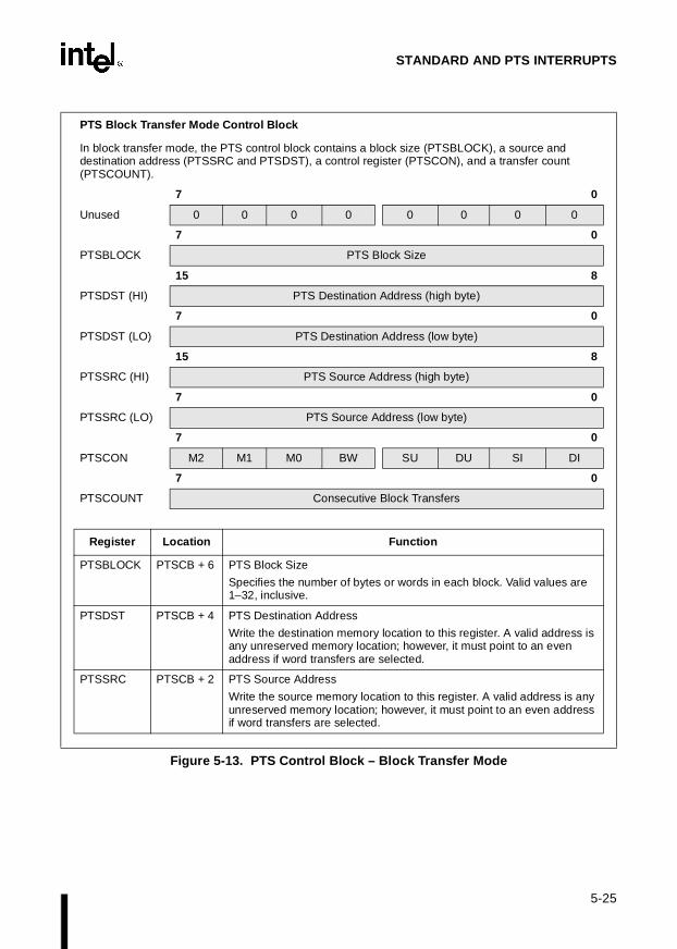
5-25
STANDARD AND PTS INTERRUPTS
PTS Block Transfer Mode Control Block
In block transfer mode, the PTS control block contains a block size (PTSBLOCK), a source and destination address (PTSSRC and PTSDST), a control register (PTSCON), and a transfer count (PTSCOUNT).
7 0
Unused 0 0 0 0 0 0 0 0
7 0
PTSBLOCK PTS Block Size
15 8
PTSDST (HI) PTS Destination Address (high byte)
7 0
PTSDST (LO) PTS Destination Address (low byte)
15 8
PTSSRC (HI) PTS Source Address (high byte)
7 0
PTSSRC (LO) PTS Source Address (low byte)
7 0
PTSCON M2 M1 M0 BW SU DU SI DI
7 0
PTSCOUNT Consecutive Block Transfers
Register Location Function
PTSBLOCK PTSCB + 6 PTS Block Size
Specifies the number of bytes or words in each block. Valid values are 1–32, inclusive.
PTSDST PTSCB + 4 PTS Destination Address
Write the destination memory location to this register. A valid address is any unreserved memory location; however, it must point to an even address if word transfers are selected.
PTSSRC PTSCB + 2 PTS Source Address
Write the source memory location to this register. A valid address is any unreserved memory location; however, it must point to an even address if word transfers are selected.
Figure 5-13. PTS Control Block – Block Transfer Mode

8XC196Kx, Jx, CA USER’S MANUAL
5-26
5.6.5 A/D Scan Mode
In the A/D scan mode, the PTS causes the A/D converter to perform multiple conversions on oneor more channels and then stores the results in a table in memory. Figure 5-14 shows the PTS con-trol block for A/D scan mode.
Register Location Function
PTSCON PTSCB + 1 PTS Control Bits
M2:0 PTS Mode
These bits select the PTS mode:
M2 M1 M00 0 0 block transfer mode
BW Byte/Word Transfer
0 = word transfer1 = byte transfer
SU Update PTSSRC
0 = reload original PTS source address after each block transfer is complete
1 = retain current PTS source address after each block transfer is complete
DU Update PTSDST
0 = reload original PTS destination address after each block transfer is complete
1 = retain current PTS destination address after each block transfer is complete
SI PTSSRC Autoincrement
0 = do not increment the contents of PTSSRC1 = increment the contents of PTSSRC after each byte or word
transfer
DI PTSDST Autoincrement
0 = do not increment the contents of PTSDST1 = increment the contents of PTSDST after each byte or word
transfer
PTSCOUNT PTSCB + 0 Consecutive Block Transfers
Defines the number of blocks that will be transferred during the block transfer routine. Each block transfer is one PTS cycle. Maximum number is 255.
PTS Block Transfer Mode Control Block (Continued)
Figure 5-13. PTS Control Block – Block Transfer Mode (Continued)
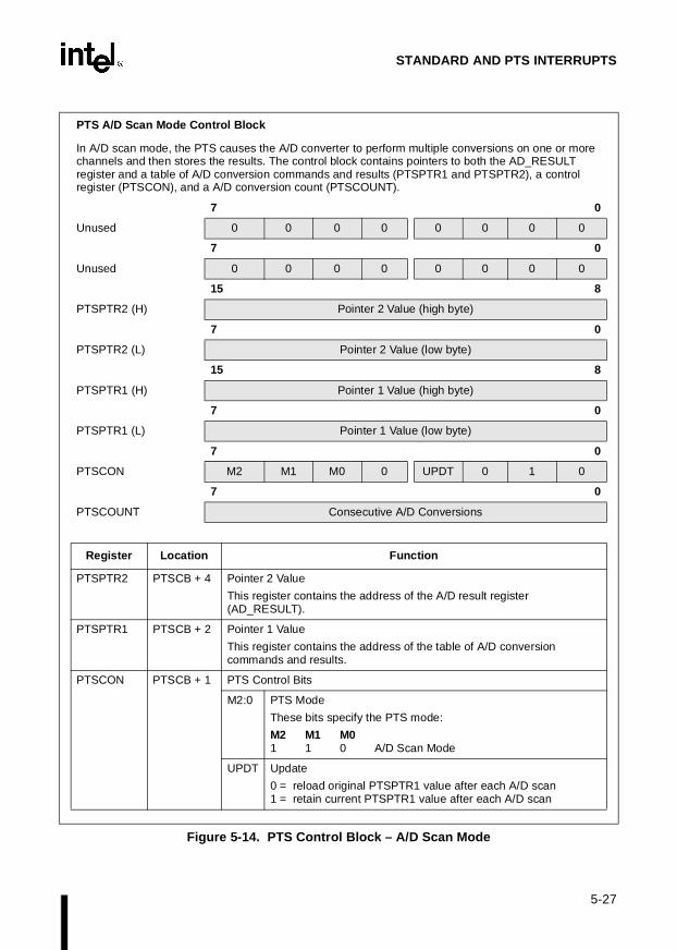
5-27
STANDARD AND PTS INTERRUPTS
PTS A/D Scan Mode Control Block
In A/D scan mode, the PTS causes the A/D converter to perform multiple conversions on one or more channels and then stores the results. The control block contains pointers to both the AD_RESULT register and a table of A/D conversion commands and results (PTSPTR1 and PTSPTR2), a control register (PTSCON), and a A/D conversion count (PTSCOUNT).
7 0
Unused 0 0 0 0 0 0 0 0
7 0
Unused 0 0 0 0 0 0 0 0
15 8
PTSPTR2 (H) Pointer 2 Value (high byte)
7 0
PTSPTR2 (L) Pointer 2 Value (low byte)
15 8
PTSPTR1 (H) Pointer 1 Value (high byte)
7 0
PTSPTR1 (L) Pointer 1 Value (low byte)
7 0
PTSCON M2 M1 M0 0 UPDT 0 1 0
7 0
PTSCOUNT Consecutive A/D Conversions
Register Location Function
PTSPTR2 PTSCB + 4 Pointer 2 Value
This register contains the address of the A/D result register (AD_RESULT).
PTSPTR1 PTSCB + 2 Pointer 1 Value
This register contains the address of the table of A/D conversion commands and results.
PTSCON PTSCB + 1 PTS Control Bits
M2:0 PTS Mode
These bits specify the PTS mode:
M2 M1 M01 1 0 A/D Scan Mode
UPDT Update
0 = reload original PTSPTR1 value after each A/D scan1 = retain current PTSPTR1 value after each A/D scan
Figure 5-14. PTS Control Block – A/D Scan Mode

8XC196Kx, Jx, CA USER’S MANUAL
5-28
To use the A/D scan mode, you must first set up a command/data table in memory (Table 5-7).The command/data table contains A/D commands that are interleaved with blank memory loca-tions. The PTS stores the conversion results in these blank locations. Only the amount of availablememory limits the table size; it can reside in internal or external RAM.
To initiate A/D scan mode, enable the A/D conversion complete interrupt and assign it to the PTS.Software must initiate the first conversion. When the A/D finishes the first conversion and gen-erates an A/D conversion complete interrupt, the interrupt vectors to the PTSCB and initiates theA/D scan routine. The PTS stores the conversion results, loads a new command intoAD_COMMAND, and then decrements the number in PTSCOUNT. As each additional conver-sion complete interrupt occurs, the PTS repeats the A/D scan cycle; it stores the conversion re-sults, loads the next conversion command into the AD_COMMAND register, and decrementsPTSCOUNT. The routine continues until PTSCOUNT decrements to zero. When this occurs,hardware clears the enable bit in the PTSSEL register, which disables PTS service, and sets thePTSSRV bit, which requests an end-of-PTS interrupt. The interrupt service routine could processthe conversion results and then re-enable PTS service for the A/D conversion complete interrupt.Because the lower six bits of the AD_RESULT register contain status information, the end-of-PTS interrupt service routine could shift the results data to the right six times to leave only theconversion results in the memory locations. See AP-445, 8XC196KR Peripherals: A User’s Pointof View, for application examples with code.
PTSCOUNT PTSCB + 0 Consecutive A/D Conversions
Defines the number of A/D conversions that will be completed during the A/D scan routine. Each cycle consists of the PTS transferring the A/D conversion results into the command/data table, and then loading a new command into the AD_COMMAND register. Maximum number is 255.
Table 5-7. A/D Scan Mode Command/Data TableXXX + 0AH A/D Result 2
XXX + 8H Unused A/D Command 3†
XXX + 6H A/D Result 1
XXX + 4H Unused A/D Command 2
XXX + 2H A/D Result 0††
XXX Unused A/D Command 1
† Write 0000H to prevent a new conversion at the end of the routine.†† Result of the A/D conversion that initiated the PTS routine.
PTS A/D Scan Mode Control Block (Continued)
Figure 5-14. PTS Control Block – A/D Scan Mode (Continued)

5-29
STANDARD AND PTS INTERRUPTS
5.6.5.1 A/D Scan Mode Cycles
Software must start the first A/D conversion. After the A/D conversion complete interrupt ini-tiates the PTS routine, the following actions occur.
1. The PTS reads the first command, stores it in a temporary location, and increments thePTSPTR1 register twice. PTSPTR1 now points to the first blank location in thecommand/data table (address XXXX + 2).
2. The PTS reads the AD_RESULT register, stores the results of the first conversion intolocation XXXX + 2 in the command/data table, and increments the PTSPTR1 registertwice. PTSPTR1 now points to XXXX + 4.
3. The PTS loads the command from the temporary location into the AD_COMMANDregister. This completes the first A/D scan cycle and initiates the next A/D conversion.
4. If UPDT (PTSCON.3) is clear, the original address is reloaded into the PTSPTR1 register.The next cycle will use the same command and overwrite previous data. If UPDT is set,the updated address remains in PTSPTR1 and the next cycle will use a new command andstore the conversion results at the new address.
5. PTSCOUNT is decremented and the CPU returns to regular program execution. When thenext A/D conversion complete interrupt occurs, the cycle repeats. When PTSCOUNTreaches zero, hardware clears the corresponding PTSSEL bit and sets the PTSSRV bit,which requests the end-of-PTS interrupt.
5.6.5.2 A/D Scan Mode Example 1
The command/data table shown in Table 5-8 sets up a series of A/D conversions, beginning withchannel 7 and ending with channel 4. Each table entry is a word (two bytes). Table 5-9 shows thecorresponding PTSCB.
Software starts a conversion on channel 7. Upon completion of the conversion, the A/D conver-sion complete interrupt initiates the A/D scan mode routine. Step 1 stores the channel 6 commandin a temporary location and increments PTSPTR1 to 3002H. Step 2 stores the result of the channel7 conversion in location 3002H and increments PTSPTR1 to 3004H. Step 3 loads the channel 6command from the temporary location into the AD_COMMAND register to start the next con-

8XC196Kx, Jx, CA USER’S MANUAL
5-30
version. Step 4 updates PTSPTR1 (PTSPTR1 now points to 3004H) and step 5 decrementsPTSCOUNT to 3. The next cycle begins by storing the channel 5 command in the temporary lo-cation. During the last cycle (PTSCOUNT = 1), the dummy command is loaded into theAD_COMMAND register and no conversion is performed. PTSCOUNT is decremented to zeroand the end-of-PTS interrupt is requested.
5.6.5.3 A/D Scan Mode Example 2
Table 5-11 sets up a series of ten PTS cycles, each of which reads a single A/D channel and storesthe result in a single location (3002H). The UPDT bit (PTSCON.3) is cleared so that original con-tents of PTSPTR1 are restored after the cycle. The command/data table is shown in Table 5-10.
Table 5-8. Command/Data Table (Example 1)
Address Contents
300EH AD_RESULT for ACH4
300CH 0000H (Dummy command)
300AH AD_RESULT for ACH5
3008H AD_COMMAND for ACH4
3006H AD_RESULT for ACH6
3004H AD_COMMAND for ACH5
3002H AD_RESULT for ACH7
3000H AD_COMMAND for ACH6
Table 5-9. A/D Scan Mode PTSCB (Example 1)
Unused
Unused
PTSPTR2 (HI) = 1FH
PTSPTR2 (LO) = AAH
PTSPTR1 (HI) = 30H
PTSPTR1 (LO) = 00H
PTSCON = CBH (Mode = 110, UPDT = 1)
PTSCOUNT = 04H
Table 5-10. Command/Data Table (Example 2)
Address Contents
3002H AD_RESULT for ACHx
3000H AD_COMMAND for ACHx

5-31
STANDARD AND PTS INTERRUPTS
Software starts a conversion on channel x. When the conversion is finished and the A/D conver-sion complete interrupt is generated, the A/D scan mode routine begins. The PTS reads the com-mand in location 3000H and stores it in a temporary location. Then it increments PTSPTR1 twiceand stores the value of the AD_RESULT register in location 3002H. The final step is to copy theconversion command from the temporary location to the AD_COMMAND register. The CPUcould process or move the conversion results data from the table before the next conversion com-pletes and a new PTS cycle begins. When the next cycle begins, PTSPTR1 again points to 3000Hand the repeats the events of the first cycle. The value of the AD_RESULT register is written tolocation 3002H and the command at location 3000H is re-executed.
5.6.6 PWM Modes
The PWM toggle and PWM remap modes are designed for use with the event processor array(EPA) to generate pulse-width modulated (PWM) output signals. These modes can also be usedwith an interrupt signal from any other source. The PWM toggle mode uses a single EPA channelto generate a PWM signal. The PWM remap mode uses two EPA channels, but it can generatesignals with duty cycles closer to 0% or 100% than are possible with the PWM toggle mode. Ta-ble 5-12 compares the two PWM modes. For code examples, see AP-445, 8XC196KR Peripher-als: A User’s Point of View and “EPA PWM Output Program” on page 10-35.
Table 5-11. A/D Scan Mode PTSCB (Example 2)
Unused
Unused
PTSPTR2 (HI) = 1FH
PTSPTR2 (LO) = AAH
PTSPTR1 (HI) = 30H
PTSPTR1 (LO) = 00H
PTSCON = C3H (Mode = 110, UPDT = 0)
PTSCOUNT = 0AH
Table 5-12. Comparison of PWM Modes
PWM Toggle Mode PWM Remap Mode
Reads the location specified by PTSPTR1 (usually EPAx_TIME).
Reads the location specified by PTSPTR1(usually EPAx_TIME).
Adds one of two values to the location specified by PTSPTR1. If TBIT is clear, it adds the value in PTSCONST1. If TBIT is set, it adds the value in PTSCONST2.
Adds the value in PTSCONST1 to the location specified by PTSPTR1.
Stores the sum back into the location specified by PTSPTR1.
Stores the sum back into the location specified by PTSPTR1.
Toggles TBIT. Toggles the unused TBIT.

8XC196Kx, Jx, CA USER’S MANUAL
5-32
Figure 5-15 illustrates a generic PWM waveform. The time the output is “on” is T1; the time theoutput is “off” is T2 – T1. The formulas for frequency and duty cycle are shown below. In mostapplications, the frequency is held constant and the duty cycle is varied to change the average val-ue of the waveform.
Frequency, in Hertz =
Duty Cycle = × 100%
Figure 5-15. A Generic PWM Waveform
The PWM modes do not use a PTSCOUNT register to specify the number of consecutive PTScycles. To stop producing the PWM output, clear the PTSSEL.x bit to disable PTS service for theinterrupt and reconfigure the EPA channel in the interrupt service routine.
5.6.6.1 PWM Toggle Mode Example
Figure 5-16 shows the PTS control block for PWM toggle mode. To generate a PWM waveformusing PWM toggle mode and EPA0, complete the following procedure. This example uses thevalues stored in CSTORE1 and CSTORE2 to control the frequency and duty cycle of a PWM.
1. Disable the interrupts and the PTS. The DI instruction disables all standard interrupts; theDPTS instruction disables the PTS.
2. Store the on-time (T1) in CSTORE1.
3. Store the off-time (T2 – T1) in CSTORE2.
1
T2-------
T1
T2-------
Output Value
1 on off on off
00 T1 T2 T2 + T1 Time, t
On-time = T1 Off-time = T2 - T1
A0263-02

5-33
STANDARD AND PTS INTERRUPTS
4. Set up the PTSCB as shown in Table 5-13:
— Load PTSCON with 43H (selects PWM toggle mode, initial TBIT value = 1)
— Set up PTSPTR1 to point to EPA0_TIME (the EPA0 event-time register)
— Load PTSCONST1 with the on-time (T1) from CSTORE1.
— Load PTSCONST2 with the off-time (T2 – T1) from CSTORE2.
5. Configure P1.0 to serve as the EPA0 output:
— Clear P1_DIR.0 (selects output)
— Set P1_MODE.0 (selects the EPA0 special-function signal)
— Set P1_REG.0 (initializes the output to “1”)
6. Set up EPA0:
— Load EPA0_CON with 0078H (timer 1, compare, toggle output pin, re-enable)
— Load EPA0_TIME with the value in PTSCONST1 (selects T1 as first event time)
— Load T1CONTROL with C2H (enables timer 1, selects up counting at FOSC/4, andenables the divide-by-four prescaler)
7. Enable the EPA0 interrupt and select PTS service for it:
— Set INT_MASK.4
— Set PTSSEL.4
8. Enable the interrupts and the PTS. The EI instruction enables interrupts; the EPTSinstruction enables the PTS.
Table 5-13. PWM Toggle Mode PTSCBPTSCONST2 (HI) = T2 – T1 (HI)
PTSCONST2 (LO) = T2 – T1 (LO)
PTSCONST1 (HI) = T1 (HI)
PTSCONST1 (LO) = T1 (LO)
PTSPTR1 (HI) = 1FH
PTSPTR1 (LO) = 62H
PTSCON = 43H (Mode = 010, TMOD = 1, TBIT = 1)
Unused
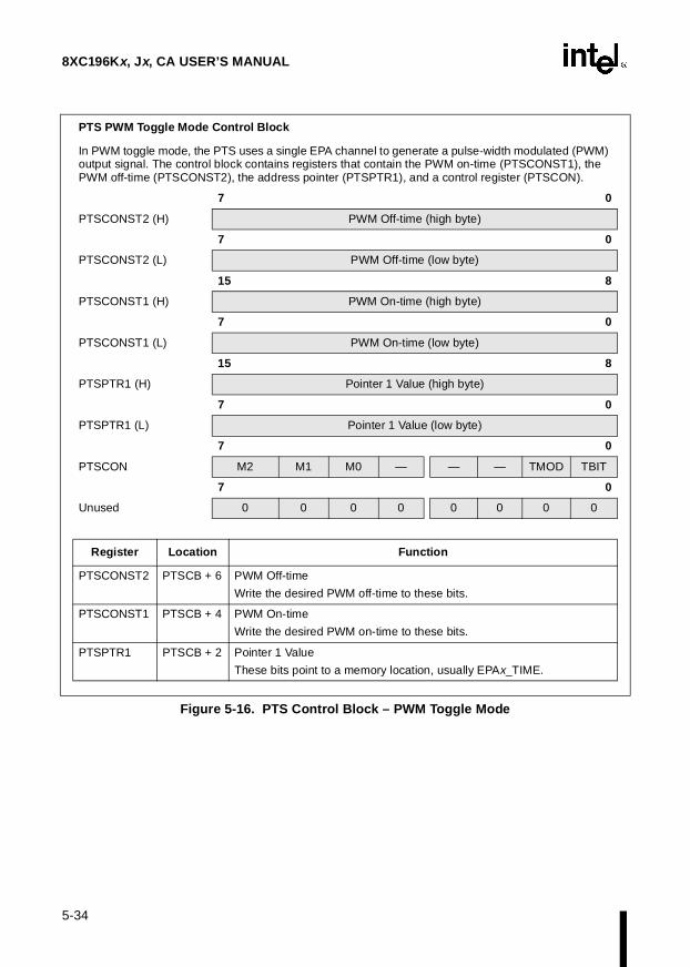
8XC196Kx, Jx, CA USER’S MANUAL
5-34
PTS PWM Toggle Mode Control Block
In PWM toggle mode, the PTS uses a single EPA channel to generate a pulse-width modulated (PWM) output signal. The control block contains registers that contain the PWM on-time (PTSCONST1), the PWM off-time (PTSCONST2), the address pointer (PTSPTR1), and a control register (PTSCON).
7 0
PTSCONST2 (H) PWM Off-time (high byte)
7 0
PTSCONST2 (L) PWM Off-time (low byte)
15 8
PTSCONST1 (H) PWM On-time (high byte)
7 0
PTSCONST1 (L) PWM On-time (low byte)
15 8
PTSPTR1 (H) Pointer 1 Value (high byte)
7 0
PTSPTR1 (L) Pointer 1 Value (low byte)
7 0
PTSCON M2 M1 M0 — — — TMOD TBIT
7 0
Unused 0 0 0 0 0 0 0 0
Register Location Function
PTSCONST2 PTSCB + 6 PWM Off-time
Write the desired PWM off-time to these bits.
PTSCONST1 PTSCB + 4 PWM On-time
Write the desired PWM on-time to these bits.
PTSPTR1 PTSCB + 2 Pointer 1 Value
These bits point to a memory location, usually EPAx_TIME.
Figure 5-16. PTS Control Block – PWM Toggle Mode

5-35
STANDARD AND PTS INTERRUPTS
Figure 5-17 is a flow diagram of the EPA and PTS operations for this example. Operation beginswhen the timer is enabled (at t = 0 in Figure 5-15 on page 5-32) by the write to T1CONTROL.The first timer match occurs at t = T1. The EPA toggles the output pin to zero and generates aninterrupt to initiate the first PTS cycle.
PWM Toggle Cycle 1. Because TBIT is initialized to one, the PTS adds the off-time (T2 –T1) to EPA0_TIME and toggles TBIT to zero.
The second timer match occurs at t = T2 (the end of one complete PWM pulse). The EPA togglesthe output to one and generates an interrupt to initiate the second PTS cycle.
PWM Toggle Cycle 2. Because TBIT is zero, the PTS adds the on-time (T1) toEPA0_TIME and toggles the TBIT to one.
The next timer match occurs at t = T2 + T1. The EPA toggles the output to zero and initiates thethird PTS cycle. The PTS actions are the same as in cycle 1, and generation of the PWM outputcontinues with PTS cycle 1 and cycle 2 alternating.
Register Location Function
PTSCON PTSCB + 1 PTS Control Bits
M2:0 PTS Mode
These bits specify the PTS mode:
M2 M1 M00 1 0 PWM
TMOD Toggle Mode Select
1 = PWM toggle mode
TBIT Toggle Bit Initial Value
Determines the initial value of TBIT.
0 = selects initial value as zero1 = selects initial value as one
The TBIT value determines whether PTSCONST1 or PTSCONST2 is added to the PTSPTR1 value:
0 = PTSCONST1 is added to PTSPTR11 = PTSCONST2 is added to PTSPTR1
Reading this bit returns the current value of TBIT, which is toggled by hardware at the end of each PWM toggle cycle.
PTS PWM Toggle Mode Control Block (Continued)
Figure 5-16. PTS Control Block – PWM Toggle Mode (Continued)

8XC196Kx, Jx, CA USER’S MANUAL
5-36
Figure 5-17. EPA and PTS Operations for the PWM Toggle Mode Example
Software can change the duty cycle during the PWM operation. When a duty cycle change is re-quired, the program writes new values of T1 and T2 – T1 to CSTORE1 and CSTORE2 and selectsnormal interrupt service for the next EPA0 interrupt. When the next timer match occurs, the out-put is toggled, and the device executes a normal interrupt service routine, which performs theseoperations:
1. The routine writes the new value of T1 (in CSTORE1) to PTSCONST1 and the new valueof T1 – T2 (in CSTORE2) to PTSCONST2.
2. It selects PTS service for the EPA0 interrupt.
A2552-02
= 1
Toggle Output
Timer Match
?
No
Yes
= 0
Toggle TBIT
EPA0_TIME = EPA0_TIME + T1 EPA0_TIME = EPA0_TIME + (T2 - T1)
Start
TBIT
EPA
PTS
A2552-02
= 1
Toggle Output
Timer Match
?
No
Yes
= 0
Toggle TBIT
EPA0_TIME = EPA0_TIME + T1 EPA0_TIME = EPA0_TIME + (T2 - T1)
Start
TBIT
EPA
PTS Cycle
5-37
STANDARD AND PTS INTERRUPTS
When the next timer match occurs, the PTS cycle (Figure 5-17) increments EPA0_TIME by T1(if TBIT is zero (output = 0)) or T2 – T1 (if TBIT is one (output = 1)). (Note that although thevalues of the EPA0 output and TBIT are the same in this example, these two values are unrelated.To establish the initial value of the output, set or clear P1_REG.x.)
The PWM toggle mode has the advantage of using only one EPA channel. However, if the wave-form edges are close together, the PTS may take too long and miss setting up the next edge. ThePWM remap mode uses two EPA channels to eliminate this problem.
5.6.6.2 PWM Remap Mode Example
Figure 5-18 shows the PTS control block for PWM remap mode. This example uses two EPAchannels and a single timer to generate a PWM waveform in PWM remap mode. EPA0 sets theoutput, and EPA1 clears it. For each channel, an interrupt is generated every T2 period, but thecomparison times for the channels are offset by the on-time, T1 (see Figure 5-15 on page 5-32).Although TBIT is toggled at the end of every PWM remap mode cycle (see Table 5-12 on page5-31), it plays no role in this mode. To generate a PWM waveform, follow this procedure.
1. Disable the interrupts and the PTS. The DI instruction disables all interrupts; the DPTSinstruction disables the PTS.
2. Set up one PTSCB for EPA0 and one for EPA1 as shown in Table 5-14. Note that the twoblocks are identical, except that PTSPTR1 points to EPA0_TIME for EPA0 and toEPA1_TIME for EPA1.
3. Configure P1.1 to serve as the EPA1 output. (Because EPA0 is not used as an output, portpin P1.0 can be used for standard I/O.)
— Clear P1_DIR.1 (selects output)
— Set P1_MODE.1 (selects the EPA0 special-function signal)
— Set P1_REG.1 (initializes the output to “1”)

8XC196Kx, Jx, CA USER’S MANUAL
5-38
4. Set up EPA0 and EPA1:
— Load EPA0_CON with 68H (timer 1, compare mode, set output pin, re-enable).
— Load EPA1_CON with 158H (timer 1, compare mode, clear output pin, re-enable,remap enabled).
— Load EPA0_TIME with 0000H (selects time 0 as first event time for EPA0).
— Load EPA1_TIME with the value of T1 (selects time T1 as first event time for EPA1).
— Load timer 1 with FFFFH to ensure that the EPA0 event time (t = 0) is matched first.
— Load T1CONTROL with C2H (enables timer 1, selects up-counting at FOSC/4, andenables the divide-by-four prescaler).
5. Enable the EPA0 and EPA1 interrupts and select PTS service for them:
— Set INT_MASK.4 and INT_MASK.3.
— Set PTSSEL.4 and PTSSEL.3
6. Enable the interrupts and the PTS. The EI instruction enables interrupts; the EPTSinstruction enables the PTS.
Table 5-14. PWM Remap Mode PTSCB
PTSCB0 for EPA0 PTSCB1 for EPA1
Unused Unused
Unused Unused
PTSCONST1 (HI) = T2 (HI) PTSCONST1 (HI) = T2 (HI)
PTSCONST1 (LO) = T2 (LO) PTSCONST1 (LO) = T2 (LO)
PTSPTR1 (HI) = 1FH (EPA0_TIME, HI) PTSPTR1 (HI) = 1FH (EPA1_TIME, HI)
PTSPTR1 (LO) = 62H (EPA0_TIME, LO) PTSPTR1 (LO) = 66H (EPA1_TIME, LO)
PTSCON = 40H (Mode = 010, TMOD = 0) PTSCON = 40H (Mode = 010, TMOD = 0)
Unused Unused

5-39
STANDARD AND PTS INTERRUPTS
PTS PWM Remap Mode Control Block
In PWM remap mode, the PTS uses two EPA channels to generate a pulse-width modulated (PWM) output signal. The control block contains registers that contain the PWM on-time (PTSCONST1), the address pointer (PTSPTR1), and a control register (PTSCON).
7 0
Unused 0 0 0 0 0 0 0 0
7 0
Unused 0 0 0 0 0 0 0 0
15 8
PTSCONST1 (HI) PWM Const 1 Value (high byte)
7 0
PTSCONST1 (LO) PWM Const 1 Value (low byte)
15 8
PTSPTR1 (HI) Pointer 1 Value (high byte)
7 0
PTSPTR1 (LO) Pointer 1 Value (low byte)
7 0
PTSCON M2 M1 M0 — — — TMOD TBIT
7 0
Unused 0 0 0 0 0 0 0 0
Register Location Function
PTSCONST1 PTSCB + 4 PWM Const 1 Value
Write the desired PWM on-time to these bits.
PTSPTR1 PTSCB + 2 Pointer 1 Value
These bits point to a memory location, usually EPAx_TIME.
Figure 5-18. PTS Control Block – PWM Remap Mode

8XC196Kx, Jx, CA USER’S MANUAL
5-40
Figure 5-19 shows the EPA and PTS operations for this example. The first timer match occurs att = 0 for EPA0, which sets the output and generates an interrupt.
PWM Remap Cycle 1. The PTS adds T2 to EPA0_TIME and toggles the TBIT.
The output remains set until the second timer match occurs at T1 for EPA1, which clears the out-put and generates an interrupt.
PWM Remap Cycle 2. The PTS adds T2 to EPA1_TIME and toggles the TBIT.
Alternating EPA0 and EPA1 interrupts continue, with EPA0 setting the output and EPA1 clearingit.
Register Location Function
PTSCON PTSCB + 1 PTS Control Bits
M2:0 PTS Mode
These bits specify the PTS mode:
M2 M1 M00 1 0 PWM
TMOD Remap Mode Select
0 = PWM remap mode
TBIT Toggle Bit Initial Value
Determines the initial value of TBIT.
1 = selects initial value as one0 = selects initial value as zero
The TBIT value determines whether PTSCONST1 or PTSCONST2 is added to the PTSPTR1 value:
1 = PTSCONST2 is added to PTSPTR10 = PTSCONST1 is added to PTSPTR1
Reading this bit returns the current value of TBIT, which is toggled by hardware at the end of each PWM remap cycle.
In PWM remap mode, the TBIT value is not used; PTSCONST1 is always added to the PTSPTR1 value. However, the unused TBIT still toggles at the end of each PWM remap cycle.
PTS PWM Remap Mode Control Block (Continued)
Figure 5-18. PTS Control Block – PWM Remap Mode (Continued)
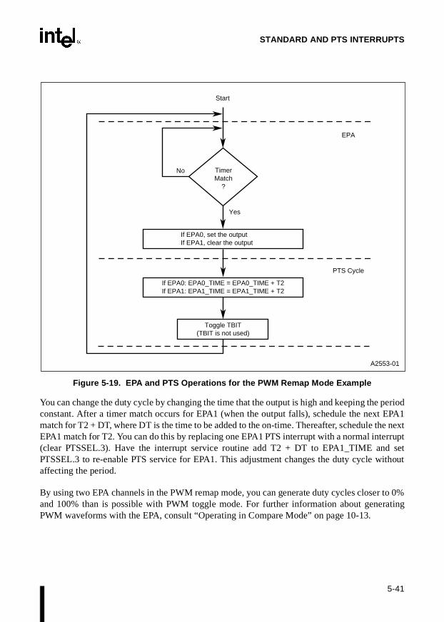
5-41
STANDARD AND PTS INTERRUPTS
Figure 5-19. EPA and PTS Operations for the PWM Remap Mode Example
You can change the duty cycle by changing the time that the output is high and keeping the periodconstant. After a timer match occurs for EPA1 (when the output falls), schedule the next EPA1match for T2 + DT, where DT is the time to be added to the on-time. Thereafter, schedule the nextEPA1 match for T2. You can do this by replacing one EPA1 PTS interrupt with a normal interrupt(clear PTSSEL.3). Have the interrupt service routine add T2 + DT to EPA1_TIME and setPTSSEL.3 to re-enable PTS service for EPA1. This adjustment changes the duty cycle withoutaffecting the period.
By using two EPA channels in the PWM remap mode, you can generate duty cycles closer to 0%and 100% than is possible with PWM toggle mode. For further information about generatingPWM waveforms with the EPA, consult “Operating in Compare Mode” on page 10-13.
A2553-01
Timer Match
?
No
Yes
Toggle TBIT (TBIT is not used)
Start
EPA
PTS
If EPA0: EPA0_TIME = EPA0_TIME + T2 If EPA1: EPA1_TIME = EPA1_TIME + T2
If EPA0, set the output If EPA1, clear the output
A2553-01
Timer Match
?
No
Yes
Toggle TBIT (TBIT is not used)
Start
EPA
PTS Cycle
If EPA0: EPA0_TIME = EPA0_TIME + T2 If EPA1: EPA1_TIME = EPA1_TIME + T2
If EPA0, set the output If EPA1, clear the output


6I/O Ports

6-1
CHAPTER 6I/O PORTS
I/O ports provide a mechanism to transfer information between the device and the surroundingsystem circuitry. They can read system status, monitor system operation, output device status,configure system options, generate control signals, provide serial communication, and so on.Their usefulness in an application is limited only by the number of I/O pins available and theimagination of the engineer.
6.1 I/O PORTS OVERVIEW
Standard I/O port registers are located in the SFR address space and they can be windowed. Mem-ory-mapped I/O port registers are located in memory-mapped address space. They are indirectlyaddressable only, and they cannot be windowed. All ports can provide low-speed input/outputpins or serve alternate functions. Table 6-1 provides an overview of the device I/O ports. The re-mainder of this chapter describes the ports in more detail and explains how to configure the pins.The chapters that cover the associated peripherals discuss using the pins for their special func-tions.
6.2 INPUT-ONLY PORT 0
Port 0 is an eight-bit, high-impedance, input-only port. Its pins can be read as digital inputs; theyare also inputs to the A/D converter. Port 0 differs from the other ports in that its pins can be usedonly as inputs to the digital or analog circuitry.
Table 6-1. Device I/O Ports
Port Bits Type Direction Associated Peripheral(s)
Port 0 8 (Kx)6 (CA, Jx) Standard Input-only A/D converter
Port 1 8 (Kx)4 (CA, Jx) Standard Bidirectional EPA and timers
Port 2 8 (Kx)6 (CA, Jx) Standard Bidirectional SIO, interrupts, bus control, clock gen.
Port 3 8 Memory-mapped Bidirectional Address/data bus
Port 4 8 Memory-mapped Bidirectional Address/data bus
Port 5 8 Memory-mapped Bidirectional Bus control, slave port
Port 6 8 Standard Bidirectional EPA, SSIO

8XC196Kx, Jx, CA USER’S MANUAL
6-2
Because port 0 is permanently configured as an input-only port, it has no configuration registers.Its single register, P0_PIN, can be read to determine the current state of the pin. The register isbyte-addressable and can be windowed. (See Chapter 4, “Memory Partitions.”)
Table 6-2 lists the standard input-only port pins and Table 6-3 describes the P0_PIN status regis-ter.
6.2.1 Standard Input-only Port Operation
Figure 6-1 is a schematic of an input-only port pin. Transistors Q1 and Q2 serve as electrostaticdischarge (ESD) protection devices; they are referenced to VREF and ANGND. Transistor Q3 isan additional ESD protection device; it is referenced to VSS (digital ground). Resistor R1 limitscurrent flow through Q3 to acceptable levels. At this point, the input signal is sent to the analogmultiplexer and to the digital level-translation buffer. The level-translation buffer converts the in-put signals to work with the VCC and VSS digital voltage levels used by the CPU core. This bufferis Schmitt-triggered for improved noise immunity. The signals are latched in the P0_PIN registerand are output onto the internal bus when P0_PIN is read.
Table 6-2. Standard Input-only Port Pins
Port Pin Special-function Signal(s)
Special-function Signal Type
AssociatedPeripheral
P0.7:0 (Kx), P0.7:2 (CA, Jx)
ACH7:0 (Kx), ACH7:2 (CA, Jx)
Input A/D converter
Table 6-3. Input-only Port Registers
Mnemonic Address Description
P0_PIN 1FDAH Port 0 Input
Each bit of P0_PIN reflects the current state of the corresponding port 0 pin.

6-3
I/O PORTS
Figure 6-1. Standard Input-only Port Structure
6.2.2 Standard Input-only Port Considerations
Port 0 pins are unique in that they may individually be used as digital inputs and analog inputs atthe same time. However, reading the port induces noise into the A/D converter, decreasing theaccuracy of any conversion in progress. We strongly recommend that you not read the port whilean A/D conversion is in progress. To reduce noise, the P0_PIN register is clocked only when theport is read.
These port pins are powered by the analog reference voltage (VREF) and analog ground (ANGND)pins. If the port pins are to function as either analog or digital inputs, the VREF and ANGND pinsmust provide power. If the voltage applied to the analog input exceeds VREF or ANGND by morethan 0.5 volts, current will be driven through Q1 or Q2 into the reference circuitry, decreasing theaccuracy of all analog conversions.
The port pin is sampled one state time before the read buffer is enabled. Sampling occurs duringphase 1 (while CLKOUT is low) and resolves the value of the pin before it is presented to theinternal bus. To ensure that the value is recognized, it must be valid 45 ns before the rising edgeof CLKOUT and must remain valid until CLKOUT falls. If the pin value changes during the sam-ple time, the new value may or may not be recorded.
As a digital input, a pin acts as a high-impedance input. However, as an analog input, a pin mustprovide current for a short time to charge the internal sample capacitor when a conversion begins.This means that if a conversion is taking place on a port pin, its input characteristics change mo-mentarily.
VREF
Q3
Q1LevelTranslation
Buffer
PH1 Clock
PORT 0 Data Register
Internal Bus
P0_PIN
DQ
VREF
Vss
150 to 200 Ohms
Q2
ANGNDANGND
To Analog MUX
VssVss
Vcc
Buffer
Read Port
R1LE
Input Pin
A0236-01

8XC196Kx, Jx, CA USER’S MANUAL
6-4
6.3 BIDIRECTIONAL PORTS 1, 2, 5, AND 6
Although the bidirectional ports are very similar in both circuitry and configuration, port 5 differsfrom the others in some ways. Port 5, a memory-mapped port, uses a standard CMOS input bufferbecause of the high speeds required for system control functions. The remaining bidirectionalports use Schmitt-triggered input buffers for improved noise immunity.
NOTE
Ports 3 and 4 are significantly different from the other bidirectional ports. See “Bidirectional Ports 3 and 4 (Address/Data Bus)” on page 6-15 for details on the structure and operation of these ports.
Table 6-4 lists the bidirectional port pins with their special-function signals and associated periph-erals.
Table 6-4. Bidirectional Port Pins
Port Pin Special-functionSignal(s)
Special-functionSignal Type
Associated Peripheral
P1.0EPA0 I/O EPA
T2CLK I Timer 2
P1.1 EPA1 I/O EPA
P1.2EPA2 I/O EPA
T2DIR I Timer 2
P1.3 EPA3 I/O EPA
P1.4† EPA4 I/O EPA
P1.5† EPA5 I/O EPA
P1.6† EPA6 I/O EPA
P1.7† EPA7 I/O EPA
P2.0 TXD O SIO
P2.1 RXD I/O SIO
P2.2 EXTINT I Interrupts
P2.3† BREQ# O Bus controller
P2.4 INTOUT# O Interrupts
P2.5† HOLD# I Bus controller
P2.6 HLDA# O Bus controller
P2.7 CLKOUT O Clock generator
P5.0ALE/ADV# O Bus controller
SLPALE I Slave port†This pin is not implemented on 8XC196Jx and 87C196CA devices.††This pin is not implemented on 8XC196Jx devices.†††P5.4/SLPINT is not implemented on 8XC196Jx devices. P5.4 is implemented on the 87C196CA as a low-speed input/output pin (but it is not multiplexed with SLPINT).

6-5
I/O PORTS
Table 6-5 lists the registers associated with the bidirectional ports. Each port has three control reg-isters (Px_MODE, Px_DIR, and Px_REG); they can be both read and written. The Px_PIN regis-ter is a status register that returns the logic level present on the pins; it can only be read. Theregisters for the standard ports are byte-addressable and can be windowed. The port 5 registersmust be accessed using 16-bit addressing and cannot be windowed. “Bidirectional Port Consid-erations” on page 6-12 discusses special considerations for reading P2_REG.7 and P6_REG.7:4.
P5.1†INST O Bus controller
SLPCS# I Slave port
P5.2WR#/WRL# O Bus controller
SLPWR# I Slave port
P5.3RD# O Bus controller
SLPRD# I Slave port
P5.4††† SLPINT††† O Slave port
P5.5†† BHE#/WRH# O Bus controller
P5.6†† READY I Bus controller
P5.7†† BUSWIDTH I Bus controller
P6.0 EPA8 I/O EPA
P6.1 EPA9 I/O EPA
P6.2† T1CLK I Timer 1
P6.3† T1DIR I Timer 1
P6.4 SC0 I/O SSIO0
P6.5 SD0 I/O SSIO0
P6.6 SC1 I/O SSIO1
P6.7 SD1 I/O SSIO1
Table 6-5. Bidirectional Port Control and Status Registers
Mnemonic Address Description
P1_DIRP2_DIRP5_DIRP6_DIR
1FD2H 1FCBH 1FF3H 1FD3H
Port x Direction
Each bit of Px_DIR controls the direction of the corresponding pin.
0 =complementary output (output only)1 =input or open-drain output (input, output, or bidirectional)
Open-drain outputs require external pull-ups.
Table 6-4. Bidirectional Port Pins (Continued)
Port Pin Special-functionSignal(s)
Special-functionSignal Type
Associated Peripheral
†This pin is not implemented on 8XC196Jx and 87C196CA devices.††This pin is not implemented on 8XC196Jx devices.†††P5.4/SLPINT is not implemented on 8XC196Jx devices. P5.4 is implemented on the 87C196CA as a low-speed input/output pin (but it is not multiplexed with SLPINT).

8XC196Kx, Jx, CA USER’S MANUAL
6-6
6.3.1 Bidirectional Port Operation
Figure 6-2 shows the logic for driving the output transistors, Q1 and Q2. Q1 can source at least–3 mA at VCC – 0.7 volts. Q2 can sink at least 3 mA at 0.45 volts. (Consult the datasheet for spec-ifications.)
In I/O mode (selected by clearing Px_MODE.y), Px_REG and Px_DIR are input to the multiplex-ers. These signals combine to drive the gates of Q1 and Q2 so that the output is high, low, or highimpedance. Table 6-6 is a logic table for I/O operation of these ports.
In special-function mode (selected by setting Px_MODE.y), SFDIR and SFDATA are input to themultiplexers. These signals combine to drive the gates of Q1 and Q2 so that the output is high,low, or high impedance. Special-function output signals clear SFDIR; special-function input sig-nals set SFDIR. Table 6-7 is a logic table for special-function operation of these ports. Even if apin is to be used in special-function mode, you must still initialize the pin as an input or outputby writing to Px_DIR.
P1_MODE P2_MODEP5_MODEP6_MODE
1FD0H1FC9H1FF1H1FD1H
Port x Mode
Each bit of Px_MODE controls whether the corresponding pin functions as a standard I/O port pin or as a special-function signal.
0 = standard I/O port pin1 = special-function signal
P1_PINP2_PINP5_PINP6_PIN
1FD6H1FCFH1FF7H1FD7H
Port x Input
Each bit of Px_PIN reflects the current state of the corresponding pin, regardless of the pin configuration.
P1_REG P2_REGP5_REGP6_REG
1FD4H1FCDH1FF5H1FD5H
Port x Data Output
For an input, set the corresponding Px_REG bit.
For an output, write the data to be driven out by each pin to the corresponding bit of Px_REG. When a pin is configured as standard I/O (Px_MODE.x=0), the result of a CPU write to Px_REG is immediately visible on the pin. When a pin is configured as a special-function signal (Px_MODE.x=1), the associated on-chip peripheral or off-chip component controls the pin. The CPU can still write to Px_REG, but the pin is unaffected until it is switched back to its standard I/O function.
This feature allows software to configure a pin as standard I/O (clear Px_MODE.x), initialize or overwrite the pin value, then configure the pin as a special-function signal (set Px_MODE.x). In this way, initial-ization, fault recovery, exception handling, etc., can be done without changing the operation of the associated peripheral.
Table 6-5. Bidirectional Port Control and Status Registers (Continued)
Mnemonic Address Description

6-7
I/O PORTS
Resistor R1 provides ESD protection for the pin. Input signals are buffered. The standard portsuse Schmitt-triggered buffers for improved noise immunity. Port 5 uses a standard input bufferbecause of the high speeds required for system control functions. The signals are latched into thePx_PIN sample latch and output onto the internal bus when the Px_PIN register is read.
The falling edge of RESET# turns on transistor Q3, which remains on for about 300 ns, causingthe pin to change rapidly to its reset state. The active-low level of RESET# turns on transistor Q4,which weakly holds the pin high. (Q4 can source approximately –10 µA; consult the datasheetfor exact specifications.) Q4 remains on, weakly holding the pin high, until your software writesto the Px_MODE register.
NOTE (8XC196CA, JQ, JR, JT, JV, KQ, KR)
P2.7 is an exception. After reset, P2.7 carries the CLKOUT signal (half the crystal input frequency) rather than being held high. When CLKOUT is selected, it is always a complementary output.
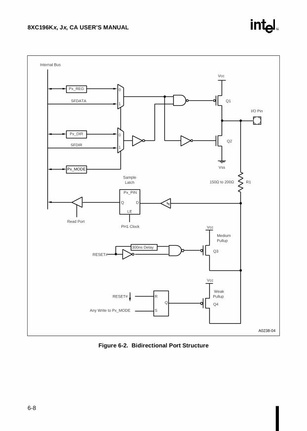
8XC196Kx, Jx, CA USER’S MANUAL
6-8
Figure 6-2. Bidirectional Port Structure
Vcc
Q2
Q1
Px_REG
Px_DIR
SampleLatch
PH1 Clock
Internal Bus
SFDATA
SFDIR
Px_MODE
Px_PIN
DQ
0
1
0
1
Vcc
Vcc
Q
R
SAny Write to Px_MODE
WeakPullup
MediumPullup
RESET#
RESET#
Q3
Q4
Vss
Read Port
LE
300ns Delay
I/O Pin
A0238-04
150Ω to 200Ω R1

6-9
I/O PORTS
Table 6-6. Logic Table for Bidirectional Ports in I/O Mode
Configuration Complementary Output Open-drain Output Input
Px_MODE 0 0 0 0
Px_DIR 0 0 1 1
SFDIR X X X X
SFDATA X X X X
Px_REG 0 1 0, 1 (Note 2) 1
Q1 off on off off
Q2 on off on, off (Note 2) off
Px_PIN 0 1 X (Note 3) high-impedance (Note 4)
NOTES:1. X = Don’t care.2. If Px_REG is cleared, Q2 is on; if Px_REG is set, Q2 is off.3. Px_PIN contains the current value on the pin.4. During reset and until the first write to Px_MODE, Q3 is on.
Table 6-7. Logic Table for Bidirectional Ports in Special-function Mode
Configuration Complementary Output Open-drain Output Input
Px_MODE 1 1 1 1
Px_DIR 0 0 1 1
SFDIR 0 0 1 1
SFDATA 0 1 0, 1 (Note 2) 1
Px_REG X X X 1
Q1 off on off off
Q2 on off on, off (Note 2) off
Px_PIN 0 1 X (Note 3) high-impedance (Note 4)
NOTES:1. X = Don’t care.2. If Px_REG is cleared, Q2 is on; if Px_REG is set, Q2 is off.3. Px_PIN contains the current value on the pin.4. During reset and until the first write to Px_MODE, Q3 is on.
8XC196Kx, Jx, CA USER’S MANUAL
6-10
6.3.2 Bidirectional Port Pin Configurations
Each bidirectional port pin can be individually configured to operate either as an I/O pin or as apin for a special-function signal. In the special-function configuration, the signal is controlled byan on-chip peripheral or an off-chip component. In either configuration, two modes are possible:
• complementary output (output only)
• high-impedance input or open-drain output (input, output, or bidirectional)
To prevent the CMOS inputs from floating, the bidirectional port pins are weakly pulled high dur-ing and after reset, until your software writes to Px_MODE. The default values of the control reg-isters after reset configure the pins as high-impedance inputs with weak pull-ups. To ensure thatthe ports are initialized correctly and that the weak pull-ups are turned off, follow this suggestedinitialization sequence:
1. Write to Px_DIR to establish the individual pins as either inputs or outputs. (Outputs willdrive the data that you specify in step 3.)
— For a complementary output, clear its Px_DIR bit.
— For a high-impedance input or an open-drain output, set its Px_DIR bit. (Open-drainoutputs require external pull-ups.)
2. Write to Px_MODE to select either I/O or special-function mode. Writing to Px_MODE(regardless of the value written) turns off the weak pull-ups. Even if the entire port is to beused as I/O (its default configuration after reset), you must write to Px_MODE to ensurethat the weak pull-ups are turned off.
— For a standard I/O pin, clear its Px_MODE bit. In this mode, the pin is driven asdefined in steps 1 and 3.
— For a special-function signal, set its Px_MODE bit. In this mode, the associatedperipheral controls the pin.
3. Write to Px_REG.
— For output pins defined in step 1, write the data that is to be driven by the pins to thecorresponding Px_REG bits. For special-function outputs, the value is immaterialbecause the peripheral controls the pin. However, you must still write to Px_REG toinitialize the pin.
— For input pins defined in step 1, set the corresponding Px_REG bits.
Table 6-8 lists the control register values for each possible configuration. For special-functionoutputs, the Px_REG value is immaterial (don’t care) because the associated peripheral controlsthe pin in special-function mode. However, you must still write to Px_REG to initialize the pin.For a bidirectional pin to function as an input (either special function or port pin), you must setPx_REG.

6-11
I/O PORTS
6.3.3 Bidirectional Port Pin Configuration Example
Assume that you wish to configure the pins of a bidirectional port as shown in Table 6-9.
To do so, you could use the following example code segment. Table 6-10 shows the state of eachpin after reset and after execution of each line of the example code.
LDB Px_DIR,#00011111BLDB Px_MODE,#00000000BLDB Px_REG,#10010011B
Table 6-8. Control Register Values for Each Configuration
Desired Pin Configuration Configuration Register Settings
Standard I/O Signal P x_DIR Px_MODE † Px_REG
Complementary output, driving 0 0 0 0
Complementary output, driving 1 0 0 1
Open-drain output, strongly driving 0 1 0 0
Open-drain output, high-impedance 1 0 1
Input 1 0 1
Special-function signal P x_DIR Px_MODE † Px_REG
Complementary output, output value controlled by peripheral 0 1 X
Open-drain output, output value controlled by peripheral 1 1 X
Input 1 1 1† During reset and until the first write to Px_MODE, the pins are weakly held high.
Table 6-9. Port Configuration E xample
Port Pin(s) Configuration Data
Px.0, Px.1 high-impedance input high-impedance
Px.2, Px.3 open-drain output 0
Px.4 open-drain output 1 (assuming external pull-up)
Px.5, Px.6 complementary output 0
Px.7 complementary output 1

8XC196Kx, Jx, CA USER’S MANUAL
6-12
6.3.4 Bidirectional Port Considerations
This section outlines special considerations for using the pins of these ports.
Port 1 After reset, your software must configure the device to match theexternal system. This is accomplished by writing appropriate config-uration data into P1_MODE. Writing to P1_MODE not onlyconfigures the pins but also turns off the transistor that weakly holdsthe pins high (Q4 in Figure 6-2 on page 6-8). For this reason, even ifport 1 is to be used as it is configured at reset, you should still writedata into P1_MODE.
Port 2 After reset, your software must configure the device to match theexternal system. This is accomplished by writing appropriate config-uration data into P2_MODE. Writing to P2_MODE not onlyconfigures the pins but also turns off the transistor that weakly holdsthe pins high (Q4 in Figure 6-2 on page 6-8). For this reason, even ifport 2 is to be used as it is configured at reset, you should still writedata into P2_MODE.
P2.2/EXTINT Writing to P2_MODE.2 sets the EXTINT interrupt pending bit. Afterconfiguring the port pins, clear the interrupt pending register beforeenabling interrupts. See “Design Considerations for ExternalInterrupt Inputs” on page 6-15.
P2.5/HOLD# 8XC196Kx Only: If P2.5 is configured as a standard I/O port pin,the device does not recognize signals on this pin as HOLD#. Instead,the bus controller receives an internal HOLD signal. This enables thedevice to access the external bus while it is performing I/O at P2.5.
Table 6-10. Port Pin States After Reset and After Example Code Execution
Action or CodeResulting Pin States †
Px.7 Px.6 Px.5 Px.4 Px.3 Px.2 Px.1 Px.0
Reset wk1 wk1 wk1 wk1 wk1 wk1 wk1 wk1
LDB Px_DIR, #00011111B 1 1 1 wk1 wk1 wk1 wk1 wk1
LDB Px_MODE, #00000000B 1 1 1 HZ1 HZ1 HZ1 HZ1 HZ1
LDB Px_REG, #10010011B 1 0 0 HZ1 0 0 HZ1 HZ1
† wk1 = weakly pulled high, HZ1 = high impedance (actually a “1” with an external pull-up).

6-13
I/O PORTS
P2.6/HLDA# The HLDA# pin is used in systems with more than one processorusing the system bus. This device asserts HLDA# to indicate that ithas freed the bus in response to HOLD# and another processor cantake control. (This signal is active low to avoid misinterpretation byexternal hardware immediately after reset.)
P2.6/HLDA# is the enable pin for ONCE mode in certain 8XC196Kxdevices (see Chapter 14, “Special Operating Modes”) and one of theenable pins for Intel-reserved test modes. Because a low input duringreset could cause the device to enter ONCE mode or a reserved testmode, exercise caution if you use this pin for input. Be certain thatyour system meets the VIH specification (listed in the datasheet)during reset to prevent inadvertent entry into ONCE mode or a testmode.
P2.7/CLKOUT 8XC196CA, JQ, JR, JT, JV, KQ, KR: Following reset, P2.7 carriesthe strongly driven CLKOUT signal. It is not held high. When P2.7is configured as CLKOUT, it is always a complementary output.
8XC196KS, KT: Following reset, P2.7 is weakly held high.
P2.7 A value written to the upper bit of P2_REG (bit 7) is held in a bufferuntil the corresponding P2_MODE bit is cleared, at which time thevalue is loaded into the P2_REG bit. A value read from P2_REG.7 isthe value currently in the register, not the value in the buffer.Therefore, any change to P2_REG.7 can be read only afterP2_MODE.7 is cleared.
Port 5 After reset, the device configures port 5 to match the external system.The following paragraphs describe the states of the port 5 pins afterreset and until your software writes to the P5_MODE register.Writing to P5_MODE not only configures the pins but also turns offthe transistor that weakly holds the pins high (Q4 in Figure 6-2 onpage 6-8). For this reason, even if port 5 is to be used as it isconfigured at reset, you should still write data into P5_MODE.
P5.0/ALE If EA# is high on reset (internal access), the pin is weakly held highuntil your software writes to P5_MODE. If EA# is low on reset(external access), either ALE or ADV# is activated as a systemcontrol pin, depending on the ALE bit of CCR0. In either case, thepin becomes a true complementary output.
P5.1/INST 8XC196Kx Only: This pin remains weakly held high until yoursoftware writes configuration data into P5_MODE.
P5.2/WR#/WRL# This pin remains weakly held high until your software writes config-uration data into P5_MODE.

8XC196Kx, Jx, CA USER’S MANUAL
6-14
P5.3/RD# If EA# is high on reset (internal access), the pin is weakly held highuntil your software writes to P5_MODE. If EA# is low on reset(external access), RD# is activated as a system control pin and thepin becomes a true complementary output.
P5.4/SLPINT 8XC196Kx Only: This pin is weakly held high until your softwarewrites to P5_MODE. P5.4/SLPINT is the enable pin for ONCE modein certain 8XC196Kx devices (see Chapter 14, “Special OperatingModes”) and one of the enable pins for Intel-reserved test modes.Because a low input during reset could cause the device to enterONCE mode or a reserved test mode, exercise caution if you use thispin for input. Be certain that your system meets the VIH specification(listed in the datasheet) during reset to prevent inadvertent entry intoONCE mode or a test mode.
P5.5/BHE#/WRH# This pin is weakly held high until the CCB fetch is completed. Atthat time, the state of this pin depends on the value of the BW0 bit ofthe CCRs. If BW0 is clear, the pin remains weakly held high untilyour software writes to P5_MODE. If BW0 is set, BHE# is activatedas a system control pin and the pin becomes a true complementaryoutput.
P5.6/READY 8XC196CA, Kx Only: This pin remains weakly held high until theCCB fetch is completed. At that time, the state of this pin depends onthe value of the IRC0–IRC2 bits of the CCRs. If IRC0–IRC2 are allset (111B), READY is activated as a system control pin. Thisprevents the insertion of infinite wait states upon the first access toexternal memory. For any other values of IRC0–IRC2, the pin isconfigured as I/O upon reset.
NOTEIf IRC0–IRC2 of the CCB are all set (activating READY as a system control pin) and P5_MODE.6 is cleared (configuring the pin as I/O), an external memory access may cause the processor to lock up.
P5.7/BUSWIDTH 8XC196Kx Only: This pin remains weakly held high until yoursoftware writes configuration data into P5_MODE.
P6.0–P6.7 After reset, your software must configure the device to match theexternal system. This is accomplished by writing appropriate config-uration data into P6_MODE. Writing to P6_MODE not onlyconfigures the pins but also turns off the transistor that weakly holdsthe pins high (Q4 in Figure 6-2 on page 6-8). For this reason, even ifport 6 is to be used as it is configured at reset, you should still writedata into P6_MODE.

6-15
I/O PORTS
P6.4–P6.7 A value written to any of the upper four bits of P6_REG (bits 4–7) isheld in a buffer until the corresponding P6_MODE bit is cleared, atwhich time the value is loaded into the P6_REG bit. A value readfrom a P6_REG bit is the value currently in the register, not the valuein the buffer. Therefore, any change to a P6_REG bit can be readonly after the corresponding P6_MODE bit is cleared.
6.3.5 Design Considerations for External Interrupt Inputs
To configure a port pin that serves as an external interrupt input, you must set the correspondingbits in the configuration registers (Px_DIR, Px_MODE, and Px_REG). To configureP2.2/EXTINT as an external interrupt input, we recommend the following sequence to prevent afalse interrupt request:
1. Disable interrupts by executing the DI instruction.
2. Set the Px_DIR bit.
3. Set the Px_MODE bit.
4. Set the Px_REG bit.
5. Clear the INT_PEND and INT_PEND1 bits.
6. Enable interrupts (optional) by executing the EI instruction.
6.4 BIDIRECTIONAL PORTS 3 AND 4 (ADDRESS/DATA BUS)
Ports 3 and 4 are eight-bit, bidirectional, memory-mapped I/O ports. They can be addressed onlywith indirect or indexed addressing and cannot be windowed. Ports 3 and 4 provide the multi-plexed address/data bus. In programming modes, ports 3 and 4 serve as the programming bus(PBUS). Port 3 can also serve as the slave port (8XC196Kx only). Port 5 supplies the bus-controlsignals.
During external memory bus cycles, the processor takes control of ports 3 and 4 and automatical-ly configures them as complementary output ports for driving address/data or as inputs for read-ing data. For this reason, these ports have no mode registers.
Systems with EA# tied inactive do not use the address/data bus, and systems that do use the ad-dress/data bus have idle time between external bus cycles. When the address/data bus is not inuse, you can use the ports for I/O. Like port 5, these ports use standard CMOS input buffers. How-ever, ports 3 and 4 must be configured entirely as complementary or open-drain ports; their pinscannot be configured individually. Systems with EA# tied active cannot use ports 3 and 4 as stan-dard I/O; when EA# is active, these ports will function only as the address/data bus.

8XC196Kx, Jx, CA USER’S MANUAL
6-16
Table 6-11 lists the port 3 and 4 pins with their special-function signals and associated peripher-als. Table 6-12 lists the registers that affect the function and indicate the status of ports 3 and 4.
6.4.1 Bidirectional Ports 3 and 4 (Address/Data Bus) Operation
Figure 6-3 shows the ports 3 and 4 logic. During reset, the active-low level of RESET# turns offQ1 and Q2 and turns on transistor Q4, which weakly holds the pin high. (Q4 can source approx-imately –10 µΑ at VCC – 1.0 volts; consult the datasheet for exact specifications.) Resistor R1 pro-vides ESD protection for the pin.
During normal operation, the device controls the port through BUS CONTROL SELECT, an in-ternal control signal. When the device needs to access external memory, it clears BUS CONTROLSELECT, selecting ADDRESS/DATA as the input to the multiplexer. ADDRESS/DATA thendrives Q1 and Q2 as complementary outputs. (Q1 can source at least –3 mA at VCC – 1.0 volts;Q2 can sink at least 3 mA at 0.45 volts. Consult the datasheet for exact specifications.)
Table 6-11. Ports 3 and 4 Pins
Port Pins Special-function Signal(s)
Special-function Signal Type Associated Peripheral
P3.7:0
AD7:0 I/O Address/data bus, low byte
PBUS7:0 I/O Programming bus, low byte
SLP7:0 (Kx only) I/O Slave port
P4.7:0AD15:8 I/O Address/data bus, high byte
PBUS15:8 I/O Programming bus, high byte
Table 6-12. Ports 3 and 4 Control and Status Registers
Mnemonic Address Description
P3_PINP4_PIN
1FFEH1FFFH
Port x Input
Each bit of Px_PIN reflects the current state of the corresponding pin, regardless of the pin configuration.
P3_REGP4_REG
1FFCH1FFDH
Port x Data Output
Each bit of Px_REG contains data to be driven out by the corresponding pin.
When the device requires access to external memory, it takes control of the port and drives the address/data bit onto the pin. The address/data bit replaces your output during this time. When the external access is completed, the device restores your data onto the pin.
P34_DRV 1FF4H Ports 3/4 Driver Enable Register
Bits 7 and 6 of the P34_DRV register control whether ports 3 and 4, respectively, are configured as complementary or open-drain. Setting a bit configures a port as complementary; clearing a bit configures a port as open-drain. These bits affect port operation only in I/O mode.
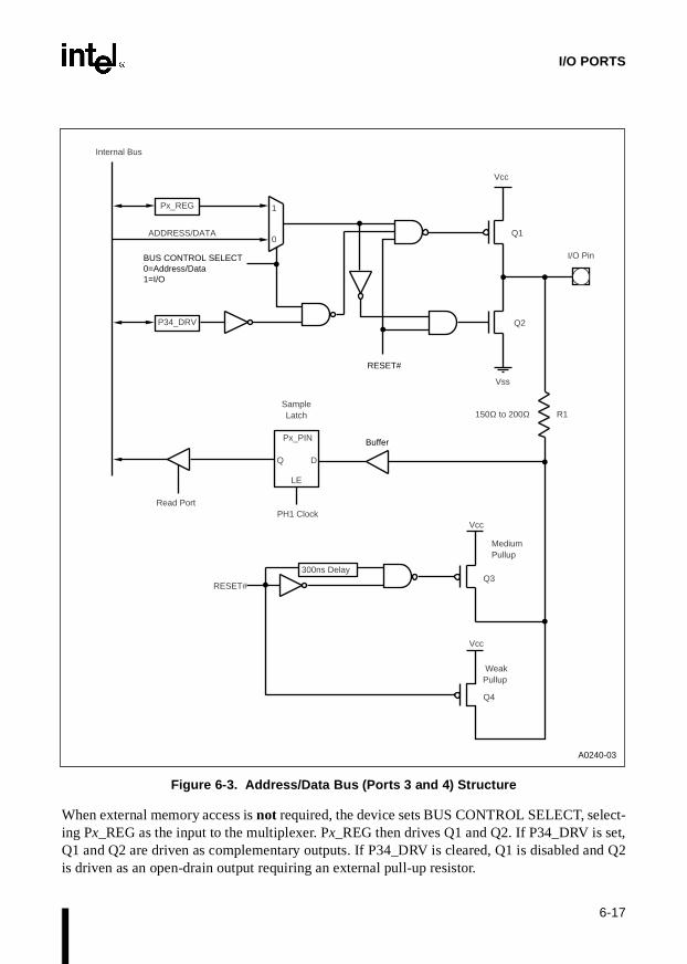
6-17
I/O PORTS
Figure 6-3. Address/Data Bus (Ports 3 and 4) Structure
When external memory access is not required, the device sets BUS CONTROL SELECT, select-ing Px_REG as the input to the multiplexer. Px_REG then drives Q1 and Q2. If P34_DRV is set,Q1 and Q2 are driven as complementary outputs. If P34_DRV is cleared, Q1 is disabled and Q2is driven as an open-drain output requiring an external pull-up resistor.
Vcc
Q2
Q1
Px_REG
P34_DRV
SampleLatch
PH1 Clock
Internal Bus
ADDRESS/DATA
Px_PIN
DQ
1
0
Vcc
Vcc
WeakPullup
MediumPullup
RESET#Q3
Q4
Buffer
Vss
Read Port
LE
300ns Delay
I/O PinBUS CONTROL SELECT 0=Address/Data 1=I/O
RESET#
A0240-03
150Ω to 200Ω R1

8XC196Kx, Jx, CA USER’S MANUAL
6-18
With the open-drain configuration (BUS CONTROL SELECT set and P34_DRV cleared) andPx_REG set, the pin can be used as an input. The signal on the pin is latched in the Px_PIN reg-ister. The pins can be read, making it easy to see which pins are driven low by the device andwhich are driven high by external drivers while in open-drain mode. Table 6-13 is a logic tablefor ports 3 and 4 as I/O.
6.4.2 Using Ports 3 and 4 as I/O
Ports 3 and 4 must be configured entirely as complementary or open-drain ports; their pins cannotbe configured individually. To configure a port, first select complementary or open-drain modeby writing to P34_DRV. Set a bit to configure the port as complementary; clear a bit to configurethe port as open-drain.
To use a port pin as an output, write the output data to the corresponding Px_REG bit. In comple-mentary mode, a pin is driven high when the corresponding Px_REG bit is set. In open-drainmode, you need to connect an external pull-up resistor. When the device requires access to exter-nal memory, it takes control of the port and drives the address/data bit onto the pin. The ad-dress/data bit replaces your output during this time. When the external access is completed, thedevice restores your data onto the pin.
To use a port pin as an input, first clear the corresponding P34_DRV bit to configure the port asopen-drain. Next, set the corresponding Px_REG bit to drive the pin to a high-impedance state.You may then read the pin’s input value in the Px_PIN register. When the device requires accessto external memory, it takes control of the port. You must configure the input source to avoid con-tention on the bus.
Table 6-13. Logic Table for Ports 3 and 4 as I/OConfiguration Complementary Open-drain
P34_DRV 1 1 0 0
Px_REG 0 1 0 1
Q1 off on off off
Q2 on off on off
Px_PIN 0 1 0 high-impedance
6-19
I/O PORTS
6.4.3 Design Considerations for Ports 3 and 4
When EA# is active, ports 3 and 4 will function only as the address/data bus. In these circum-stances, an instruction that operates on P3_REG or P4_REG causes a bus cycle that reads fromor writes to the external memory location corresponding to the SFR’s address. (For example, writ-ing to P4_REG causes a bus cycle that writes to external memory location 1FFDH.) BecauseP3_REG and P4_REG have no effect when EA# is active, the bus will float during long periodsof inactivity (such as during a BMOV or TIJMP instruction).
When EA# is inactive, ports 3 and 4 output the contents of the P3_REG and P4_REG registers.Because these registers reset to FFH and the P34_DRV register resets to 00H (open-drain mode),ports 3 and 4 will float unless you either connect external resistors to the pins, write zeros to theP3_REG and P4_REG registers, or write ones to the P34_DRV register.


7Serial I/O (SIO) Port


7-1
CHAPTER 7SERIAL I/O (SIO) PORT
A serial input/output (SIO) port provides a means for the system to communicate with externaldevices. This device has a serial I/O (SIO) port that shares pins with port 2. This chapter describesthe SIO port and explains how to configure it. Chapter 6, “I/O Ports,” explains how to configurethe port pins for their special functions. Refer to Appendix B for details about the signals dis-cussed in this chapter.
7.1 SERIAL I/O (SIO) PORT FUNCTIONAL OVERVIEW
The serial I/O port (Figure 7-1) is an asynchronous/synchronous port that includes a universalasynchronous receiver and transmitter (UART). The UART has one synchronous mode (mode 0)and three asynchronous modes (modes 1, 2, and 3) for both transmission and reception.
Figure 7-1. SIO Block Diagram
The serial port receives data into the receive buffer; it transmits data from the port through thetransmit buffer. The transmit and receive buffers are separate registers, permitting simultaneousreads and writes to both. The transmitter and receiver are buffered to support continuous trans-missions and to allow reception of a second byte before the first byte has been read.
SP_CONSP_STATUS
SBUF_TX
SBUF_RX Receive Shift Register
Transmit Shift Register
RXD
TXD
Control Logic Baud Rate Generator
TI
RIInterrupts
XTAL1
T1CLK
MSB
1
0
InternalDataBus
SP_BAUD
Note: The T1CLK clock source is unique to the 8XC196Kx. For the 8XC196CA and Jx, XTAL1 must provide the clock signal.
A3137-01

8XC196Kx, Jx, CA USER’S MANUAL
7-2
An independent, 15-bit baud-rate generator controls the baud rate of the serial port. Either XTAL1or T1CLK can provide the clock signal. The baud-rate register (SP_BAUD) selects the clocksource and the baud rate.
7.2 SERIAL I/O PORT SIGNALS AND REGISTERS
Table 7-1 describes the SIO signals and Table 7-2 describes the control and status registers.
Table 7-1. Serial Port Signals
PortPin
Serial Port Signal
Serial Port
Signal Type
Description
P2.0 TXD O Transmit Serial Data
In modes 1, 2, and 3, TXD transmits serial port output data. In mode 0, it is the serial clock output.
P2.1 RXD I/O Receive Serial Data
In modes 1, 2, and 3, RXD receives serial port input data. In mode 0, it functions as an input or an open-drain output for data.
P6.2 T1CLK † I Timer 1 Clock
External clock source for the baud-rate generator input.
† The T1CLK pin is not implemented on the 8XC196CA, JQ, JR, JT, JV devices. XTAL1 must provide the serial port clock.
Table 7-2. Serial Port Control and Status Registers
Mnemonic Address Description †
INT_MASK1 0013H Interrupt Mask 1
Setting the TI bit enables the transmit interrupt; clearing the bit disables (masks) the interrupt.
Setting the RI bit enables the receive interrupt; clearing the bit disables (masks) the interrupt.
INT_PEND1 0012H Interrupt Pending 1
When set, the TI bit indicates a pending transmit interrupt.
When set, the RI bit indicates a pending receive interrupt.
† Except as otherwise noted, write zeros to the reserved bits in these registers.†† The T1CLK pin is not implemented on the 8XC196CA, JQ, JR, JT, JV devices. XTAL1 must provide the
serial port clock.

7-3
SERIAL I/O (SIO) PORT
P2_DIR 1FCBH Port 2 Direction
This register selects the direction of each port 2 pin. Clear P2_DIR.1 to configure RXD (P2.1) as a high-impedance input/open-drain output, and set P2_DIR.0 to configure TXD (P2.0) as a comple-mentary output.
P6_DIR 1FD2H Port 6 Direction
This register selects the direction of each port 6 pin. To use T1CLK†† as the input clock to the baud-rate generator, clear P6_DIR.2.
P2_MODE 1FC9H Port 2 Mode
This register selects either the general-purpose input/output function or the peripheral function for each pin of port 2. Set P2_MODE.1:0 to configure TXD (P2.0) and RXD (P2.1) for the SIO port.
P6_MODE 1FD1H Port 6 Mode
This register selects either the general-purpose input/output function or the peripheral function for each pin of port 6. Set P6_MODE.2 to configure T1CLK†† for the SIO port.
P2_PIN 1FCFH Port 2 Pin State
Two bits of this register contain the values of the TXD (P2.0) and RXD (P2.1) pins. Read P2_PIN to determine the current value of the pins.
P6_PIN 1FD7H Port 6 Pin State
If you are using T1CLK (P6.2) as the clock source for the baud-rate generator, you can read P6_PIN.2 to determine the current value of T1CLK††.
P2_REG 1FCDH Port 2 Output Data
This register holds data to be driven out on the pins of port 2. Set P2_REG.1 for the RXD (P2.1) pin. Write the desired output data for the TXD (P2.0) pin to P2_REG.0.
P6_REG 1FD5H Port 6 Output Data
This register holds data to be driven out on the pins of port 6. To use T1CLK as the clock source for the baud-rate generator, set P6_REG.2.
SBUF_RX 1FB8H Serial Port Receive Buffer
This register contains data received from the serial port.
SBUF_TX 1FBAH Serial Port Transmit Buffer
This register contains data that is ready for transmission. In modes 1, 2, and 3, writing to SBUF_TX starts a transmission. In mode 0, writing to SBUF_TX starts a transmission only if the receiver is disabled (SP_CON.3=0)
Table 7-2. Serial Port Control and Status Registers (Continued)
Mnemonic Address Description †
† Except as otherwise noted, write zeros to the reserved bits in these registers.†† The T1CLK pin is not implemented on the 8XC196CA, JQ, JR, JT, JV devices. XTAL1 must provide the
serial port clock.
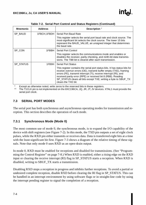
8XC196Kx, Jx, CA USER’S MANUAL
7-4
7.3 SERIAL PORT MODES
The serial port has both synchronous and asynchronous operating modes for transmission and re-ception. This section describes the operation of each mode.
7.3.1 Synchronous Mode (Mode 0)
The most common use of mode 0, the synchronous mode, is to expand the I/O capability of thedevice with shift registers (see Figure 7-2). In this mode, the TXD pin outputs a set of eight clockpulses, while the RXD pin either transmits or receives data. Data is transferred eight bits at a timewith the least-significant bit first. Figure 7-3 shows a diagram of the relative timing of these sig-nals. Note that only mode 0 uses RXD as an open-drain output.
In mode 0, RXD must be enabled for receptions and disabled for transmissions. (See “Program-ming the Control Register” on page 7-8.) When RXD is enabled, either a rising edge on the RXDinput or clearing the receive interrupt (RI) flag in SP_STATUS starts a reception. When RXD isdisabled, writing to SBUF_TX starts a transmission.
Disabling RXD stops a reception in progress and inhibits further receptions. To avoid a partial orundesired complete reception, disable RXD before clearing the RI flag in SP_STATUS. This canbe handled in an interrupt environment by using software flags or in straight-line code by usingthe interrupt pending register to signal the completion of a reception.
SP_BAUD 1FBCH,1FBDH Serial Port Baud Rate
This register selects the serial port baud rate and clock source. The most-significant bit selects the clock source. The lower 15 bits represent the BAUD_VALUE, an unsigned integer that determines the baud rate.
SP_CON 1FBBH Serial Port Control
This register selects the communications mode and enables or disables the receiver, parity checking, and ninth-bit data transmis-sions. The TB8 bit is cleared after each transmission.
SP_STATUS 1FB9H Serial Port Status
This register contains the serial port status bits. It has status bits for receive overrun errors (OE), transmit buffer empty (TXE), framing errors (FE), transmit interrupt (TI), receive interrupt (RI), and received parity error (RPE) or received bit 8 (RB8). Reading SP_STATUS clears all bits except TXE; writing a byte to SBUF_TX clears the TXE bit.
Table 7-2. Serial Port Control and Status Registers (Continued)
Mnemonic Address Description †
† Except as otherwise noted, write zeros to the reserved bits in these registers.†† The T1CLK pin is not implemented on the 8XC196CA, JQ, JR, JT, JV devices. XTAL1 must provide the
serial port clock.

7-5
SERIAL I/O (SIO) PORT
During a reception, the RI flag in SP_STATUS is set after the stop bit is sampled. The RI pendingbit in the interrupt pending register is set immediately before the RI flag is set. During a transmis-sion, the TI flag is set immediately after the end of the last (eighth) data bit is transmitted. TheTIpending bit in the interrupt pending register is generated when the TI flag in SP_STATUS is set.
Figure 7-2. Typical Shift Register Circuit for Mode 0
Figure 7-3. Mode 0 Timing
Clock Inhibit
Serial In
Shift / LOAD#Px.x
RXD
TXD
8XC196 Device
Shift Register 74HC165
Shift Register 74HC164
Inputs
Outputs
Serial In B
Clear
Px.x
Clock
Serial In A
VCC
Enable#
Clock
Data15KΩ
74HC05
Q#
A0264-02
VCC
TXD
RXD (OUT)
RXD (IN) D0
D0
D1 D2 D3 D4 D5 D6 D7
D1 D2 D3 D4 D5 D6 D7
D0
D0
D1 D2
D1
XTAL1
TXD
RXD (OUT)
RXD (IN)
Expanded:
A0109-02
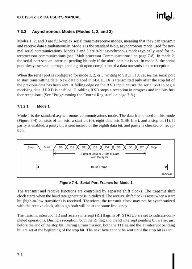
8XC196Kx, Jx, CA USER’S MANUAL
7-6
7.3.2 Asynchronous Modes (Modes 1, 2, and 3)
Modes 1, 2, and 3 are full-duplex serial transmit/receive modes, meaning that they can transmitand receive data simultaneously. Mode 1 is the standard 8-bit, asynchronous mode used for nor-mal serial communications. Modes 2 and 3 are 9-bit asynchronous modes typically used for in-terprocessor communications (see “Multiprocessor Communications” on page 7-8). In mode 2,the serial port sets an interrupt pending bit only if the ninth data bit is set. In mode 3, the serialport always sets an interrupt pending bit upon completion of a data transmission or reception.
When the serial port is configured for mode 1, 2, or 3, writing to SBUF_TX causes the serial portto start transmitting data. New data placed in SBUF_TX is transmitted only after the stop bit ofthe previous data has been sent. A falling edge on the RXD input causes the serial port to beginreceiving data if RXD is enabled. Disabling RXD stops a reception in progress and inhibits fur-ther receptions. (See “Programming the Control Register” on page 7-8.)
7.3.2.1 Mode 1
Mode 1 is the standard asynchronous communications mode. The data frame used in this mode(Figure 7-4) consists of ten bits: a start bit (0), eight data bits (LSB first), and a stop bit (1). Ifparity is enabled, a parity bit is sent instead of the eighth data bit, and parity is checked on recep-tion.
Figure 7-4. Serial Port Fr ames for Mode 1
The transmit and receive functions are controlled by separate shift clocks. The transmit shiftclock starts when the baud rate generator is initialized. The receive shift clock is reset when a startbit (high-to-low transition) is received. Therefore, the transmit clock may not be synchronizedwith the receive clock, although both will be at the same frequency.
The transmit interrupt (TI) and receive interrupt (RI) flags in SP_STATUS are set to indicate com-pleted operations. During a reception, both the RI flag and the RI interrupt pending bit are set justbefore the end of the stop bit. During a transmission, both the TI flag and the TI interrupt pendingbit are set at the beginning of the stop bit. The next byte cannot be sent until the stop bit is sent.
StartStop D0 D1 D2 D3 D4 D5 D6 D7 Stop
8 Bits of Data or 7 Bits of Data with Parity Bit
10-Bit Frame
A0245-02
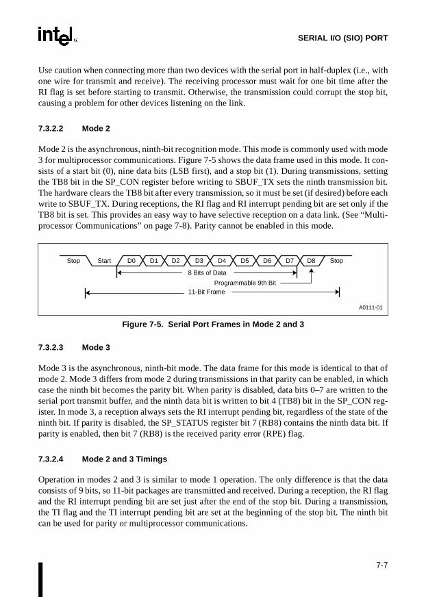
7-7
SERIAL I/O (SIO) PORT
Use caution when connecting more than two devices with the serial port in half-duplex (i.e., withone wire for transmit and receive). The receiving processor must wait for one bit time after theRI flag is set before starting to transmit. Otherwise, the transmission could corrupt the stop bit,causing a problem for other devices listening on the link.
7.3.2.2 Mode 2
Mode 2 is the asynchronous, ninth-bit recognition mode. This mode is commonly used with mode3 for multiprocessor communications. Figure 7-5 shows the data frame used in this mode. It con-sists of a start bit (0), nine data bits (LSB first), and a stop bit (1). During transmissions, settingthe TB8 bit in the SP_CON register before writing to SBUF_TX sets the ninth transmission bit.The hardware clears the TB8 bit after every transmission, so it must be set (if desired) before eachwrite to SBUF_TX. During receptions, the RI flag and RI interrupt pending bit are set only if theTB8 bit is set. This provides an easy way to have selective reception on a data link. (See “Multi-processor Communications” on page 7-8). Parity cannot be enabled in this mode.
Figure 7-5. Serial Port Frames in Mode 2 and 3
7.3.2.3 Mode 3
Mode 3 is the asynchronous, ninth-bit mode. The data frame for this mode is identical to that ofmode 2. Mode 3 differs from mode 2 during transmissions in that parity can be enabled, in whichcase the ninth bit becomes the parity bit. When parity is disabled, data bits 0–7 are written to theserial port transmit buffer, and the ninth data bit is written to bit 4 (TB8) bit in the SP_CON reg-ister. In mode 3, a reception always sets the RI interrupt pending bit, regardless of the state of theninth bit. If parity is disabled, the SP_STATUS register bit 7 (RB8) contains the ninth data bit. Ifparity is enabled, then bit 7 (RB8) is the received parity error (RPE) flag.
7.3.2.4 Mode 2 and 3 Timings
Operation in modes 2 and 3 is similar to mode 1 operation. The only difference is that the dataconsists of 9 bits, so 11-bit packages are transmitted and received. During a reception, the RI flagand the RI interrupt pending bit are set just after the end of the stop bit. During a transmission,the TI flag and the TI interrupt pending bit are set at the beginning of the stop bit. The ninth bitcan be used for parity or multiprocessor communications.
StartStop D0 D1 D2 D3 D4 D5 D6 D7 D8 Stop
8 Bits of Data
11-Bit FrameProgrammable 9th Bit
A0111-01

8XC196Kx, Jx, CA USER’S MANUAL
7-8
7.3.2.5 Multiprocessor Communications
Modes 2 and 3 are provided for multiprocessor communications. In mode 2, the serial port setsthe RI interrupt pending bit only when the ninth data bit is set. In mode 3, the serial port sets theRI interrupt pending bit regardless of the value of the ninth bit. The ninth bit is always set in ad-dress frames and always cleared in data frames.
One way to use these modes for multiprocessor communication is to set the master processor tomode 3 and the slave processors to mode 2. When the master processor wants to transmit a blockof data to one of several slaves, it sends out an address frame that identifies the target slave. Be-cause the ninth bit is set, an address frame interrupts all slaves. Each slave examines the addressbyte to check whether it is being addressed. The addressed slave switches to mode 3 to receivethe data frames, while the slaves that are not addressed remain in mode 2 and are not interrupted.
7.4 PROGRAMMING THE SERIAL PORT
To use the SIO port, you must configure the port pins to serve as special-function signals and setup the SIO channel.
7.4.1 Configuring the Serial Port Pins
Before you can use the serial port, you must configure the associated port pins to serve as special-function signals. Table 7-1 on page 7-2 lists the pins associated with the serial port. Table 7-2 liststhe port configuration registers, and Chapter 6, “I/O Ports,” explains how to configure the pins.
7.4.2 Programming the Control Register
The SP_CON register (Figure 7-6) selects the communication mode and enables or disables thereceiver, parity checking, and nine-bit data transmissions. Selecting a new mode resets the serialI/O port and aborts any transmission or reception in progress on the channel.

7-9
SERIAL I/O (SIO) PORT
SP_CON Address:Reset State:
1FBBH00H
The serial port control (SP_CON) register selects the communications mode and enables or disables the receiver, parity checking, and nine-bit data transmission.
7 0
CA, Jx, KQ, KR — — — TB8 REN PEN M1 M0
7 0
KS, KT — — PAR TB8 REN PEN M1 M0
BitNumber
BitMnemonic Function
7:6 — Reserved; always write as zeros.
5† PAR Parity Selection Bit
Selects even or odd parity.
1 = odd parity0 = even parity
4 TB8 Transmit Ninth Data Bit
This is the ninth data bit that will be transmitted in mode 2 or 3. This bit is cleared after each transmission, so it must be set before SBUF_TX is written. When SP_CON.2 is set, this bit takes on the even parity value.
3 REN Receive Enable
Setting this bit enables the receiver function of the RXD pin. When this bit is set, a high-to-low transition on the pin starts a reception in mode 1, 2, or 3. In mode 0, this bit must be clear for transmission to begin and must be set for reception to begin. Clearing this bit stops a reception in progress and inhibits further receptions.
2 PEN Parity Enable
In modes 1 and 3, setting this bit enables the parity function. This bit must be cleared if mode 2 is used. When this bit is set, TB8 takes the parity value on transmissions. With parity enabled, SP_STATUS.7 becomes the receive parity error bit.
1:0 M1:0 Mode Selection
These bits select the communications mode.
M1 M00 0 mode 00 1 mode 11 0 mode 21 1 mode 3
† This bit is reserved on the 87C196CA, 8XC196Jx, KQ, KR devices. For compatibility with future devices, write zero to this bit.
Figure 7-6. Serial Port Control (SP_CON) Register
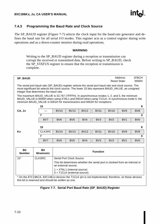
8XC196Kx, Jx, CA USER’S MANUAL
7-10
7.4.3 Programming the Baud Rate and Clock Source
The SP_BAUD register (Figure 7-7) selects the clock input for the baud-rate generator and de-fines the baud rate for all serial I/O modes. This register acts as a control register during writeoperations and as a down-counter monitor during read operations.
WARNING
Writing to the SP_BAUD register during a reception or transmission can corrupt the received or transmitted data. Before writing to SP_BAUD, check the SP_STATUS register to ensure that the reception or transmission is complete.
SP_BAUD Address:Reset State:
1FBCH0000H
The serial port baud rate (SP_BAUD) register selects the serial port baud rate and clock source. The most-significant bit selects the clock source. The lower 15 bits represent BAUD_VALUE, an unsigned integer that determines the baud rate.
The maximum BAUD_VALUE is 32,767 (7FFFH). In asynchronous modes 1, 2, and 3, the minimum BAUD_VALUE is 0000H when using XTAL1 and 0001H when using T1CLK. In synchronous mode 0, the minimum BAUD_VALUE is 0001H for transmissions and 0002H for receptions.
15 8
CA, Jx — BV14 BV13 BV12 BV11 BV10 BV9 BV8
7 0
BV7 BV6 BV5 BV4 BV3 BV2 BV1 BV0
15 8
Kx CLKSRC BV14 BV13 BV12 BV11 BV10 BV9 BV8
7 0
BV7 BV6 BV5 BV4 BV3 BV2 BV1 BV0
BitNumber
BitMnemonic Function
15† CLKSRC Serial Port Clock Source
This bit determines whether the serial port is clocked from an internal or an external source.
1 = XTAL1 (internal source)0 = T1CLK (external source)
† On the 87C196CA, 8XC196Jx devices the T1CLK pin is not implemented; therefore, on these devices this bit is reserved and should be written as one.
Figure 7-7. Serial Port Baud Rate (SP_BAUD) Regi ster

7-11
SERIAL I/O (SIO) PORT
14:0 BV14:0 These bits constitute the BAUD_VALUE.
Use the following equations to determine the BAUD_VALUE for a given baud rate.
Synchronous mode 0:††
or
Asynchronous modes 1, 2, and 3:
or
†† For mode 0 receptions, the BAUD_VALUE must be 0002H or greater. Otherwise, the resulting data in the receive shift register will be incorrect.
SP_BAUD (Co ntinued) Address:Reset State:
1FBCH0000H
The serial port baud rate (SP_BAUD) register selects the serial port baud rate and clock source. The most-significant bit selects the clock source. The lower 15 bits represent BAUD_VALUE, an unsigned integer that determines the baud rate.
The maximum BAUD_VALUE is 32,767 (7FFFH). In asynchronous modes 1, 2, and 3, the minimum BAUD_VALUE is 0000H when using XTAL1 and 0001H when using T1CLK. In synchronous mode 0, the minimum BAUD_VALUE is 0001H for transmissions and 0002H for receptions.
15 8
CA, Jx — BV14 BV13 BV12 BV11 BV10 BV9 BV8
7 0
BV7 BV6 BV5 BV4 BV3 BV2 BV1 BV0
15 8
Kx CLKSRC BV14 BV13 BV12 BV11 BV10 BV9 BV8
7 0
BV7 BV6 BV5 BV4 BV3 BV2 BV1 BV0
BitNumber
BitMnemonic Function
† On the 87C196CA, 8XC196Jx devices the T1CLK pin is not implemented; therefore, on these devices this bit is reserved and should be written as one.
Figure 7-7. Serial Port Baud Rate (SP_BAUD) Register (Continued)
BAUD_VALUEFOSC
Baud Rate 2×-------------------------------------- 1–=
T1CLK
Baud Rate----------------------------
BAUD_VALUEFOSC
Baud Rate 16×----------------------------------------- 1–=
T1CLK
Baud Rate 8×--------------------------------------

8XC196Kx, Jx, CA USER’S MANUAL
7-12
CAUTION
For mode 0 receptions, the BAUD_VALUE must be 0002H or greater. Otherwise, the resulting data in the receive shift register will be incorrect.
The reason for this restriction is that the receive shift register is clocked from an internal signal rather than the signal on TXD. Although these two signals are normally synchronized, the internal signal generates one clock before the first pulse transmitted by TXD and this first clock signal is not synchronized with TXD. This clock signal causes the receive shift register to shift in whatever data is present on the RXD pin. This data is treated as the least-significant bit (LSB) of the reception. The reception then continues in the normal synchronous manner, but the data received is shifted left by one bit because of the false LSB. The seventh data bit transmitted is received as the most-significant bit (MSB), and the transmitted MSB is never shifted into the receive shift register.
Using XTAL1 at 16 MHz, the maximum baud rates are 2.76 Mbaud (SP_BAUD = 8002H or0002H) for mode 0 and 1.0 Mbaud for modes 1, 2, and 3. Table 7-3 shows the SP_BAUD valuesfor common baud rates when using a 16 MHz XTAL1 clock input. Because of rounding, theBAUD_VALUE formula is not exact and the resulting baud rate is slightly different than desired.Table 7-3 shows the percentage of error when using the sample SP_BAUD values. In most cases,a serial link will work with up to 5.0% difference in the receiving and transmitting baud rates.
7.4.4 Enabling the Serial Port Interrupts
The serial port has both a transmit interrupt (TI) and a receive interrupt (RI). To enable an inter-rupt, set the corresponding mask bit in the interrupt mask register (see Table 7-2 on page 7-2) andexecute the EI instruction to globally enable servicing of interrupts. See Chapter 5, “Standard andPTS Interrupts,” for more information about interrupts.
Table 7-3. SP_BAUD Values When Using XTAL1 at 16 MHz
Baud RateSP_BAUD Register Value (Note 1) % Error
Mode 0 Mode 1, 2, 3 Mode 0 Mode 1, 2, 3
9600 8340H 8067H 0.04 0.16
4800 8682H 80CFH 0.02 0.16
2400 8D04H 81A0H 0.01 0.08
1200 9A0AH 8340H 0 0.04
300 E82BH 8D04H 0 0.01
NOTE: 1. Bit 15 is always set when XTAL1 is selected as the clock source for the baud-rate generator.
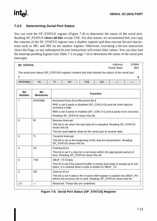
7-13
SERIAL I/O (SIO) PORT
7.4.5 Determining Serial Port Status
You can read the SP_STATUS register (Figure 7-8) to determine the status of the serial port.Reading SP_STATUS clears all bits except TXE. For this reason, we recommend that you copythe contents of the SP_STATUS register into a shadow register and then execute bit-test instruc-tions such as JBC and JBS on the shadow register. Otherwise, executing a bit-test instructionclears the flags, so any subsequent bit-test instructions will return false values. You can also readthe interrupt pending register (see Table 7-2 on page 7-2) to determine the status of the serial portinterrupts.
SP_STATUS Address:Reset State:
1FB9H0BH
The serial port status (SP_STATUS) register contains bits that indicate the status of the serial port.
7 0
RPE/RB8 RI TI FE TXE OE — —
Bit Number
Bit Mnemonic Function
7 RPE/RB8 Received Parity Error/Received Bit 8
RPE is set if parity is disabled (SP_CON.2=0) and the ninth data bit received is high.
RB8 is set if parity is enabled (SP_CON.2=1) and a parity error occurred.
Reading SP_STATUS clears this bit.
6 RI Receive Interrupt
This bit is set when the last data bit is sampled. Reading SP_STATUS clears this bit.
This bit need not be clear for the serial port to receive data.
5 TI Transmit Interrupt
This bit is set at the beginning of the stop bit transmission. Reading SP_STATUS clears this bit.
4 FE Framing Error
This bit is set if a stop bit is not found within the appropriate period of time. Reading SP_STATUS clears this bit.
3 TXE SBUF_TX Empty
This bit is set if the transmit buffer is empty and ready to accept up to two bytes. It is cleared when a byte is written to SBUF_TX.
2 OE Overrun Error
This bit is set if data in the receive shift register is loaded into SBUF_RX before the previous bit is read. Reading SP_STATUS clears this bit.
1:0 — Reserved. These bits are undefined.
Figure 7-8. Serial Port Status ( SP_STATUS) Register

8XC196Kx, Jx, CA USER’S MANUAL
7-14
The receiver checks for a valid stop bit. Unless a stop bit is found within the appropriate time, theframing error (FE) bit in the SP_STATUS register is set. When the stop bit is detected, the datain the receive shift register is loaded into SBUF_RX and the receive interrupt (RI) flag is set. Ifthis happens before the previous byte in SBUF_RX is read, the overrun error (OE) bit is set.SBUF_RX always contains the latest byte received; it is never a combination of the two bytes.
The receive interrupt (RI) flag indicates whether an incoming data byte has been received. Thetransmit interrupt (TI) flag indicates whether a data byte has finished transmitting. These flagsalso set the corresponding bits in the interrupt pending register. A reception or transmission setsthe RI or TI flag in SP_STATUS and the corresponding interrupt pending bit. However, a soft-ware write to the RI or TI flag in SP_STATUS has no effect on the interrupt pending bits and doesnot cause an interrupt. Similarly, reading SP_STATUS clears the RI and TI flags, but does notclear the corresponding interrupt pending bits. The RI and TI flags in the SP_STATUS and thecorresponding interrupt pending bits can be set even if the RI and TI interrupts are masked.
The transmitter empty (TXE) bit is set if SBUF_TX and its buffer are empty and ready to acceptup to two bytes. TXE is cleared as soon as a byte is written to SBUF_TX. One byte may be writtenif TI alone is set. By definition, if TXE has just been set, a transmission has completed and TI isset.
The received parity error (RPE) flag or the received bit 8 (RB8) flag applies for parity enabled ordisabled, respectively. If parity is enabled, RPE is set if a parity error is detected. If parity is dis-abled, RB8 is the ninth data bit received in modes 2 and 3.
7.5 PROGRAMMING EXAMPLE USING AN INTERRUPT-DRIVEN ROUTINE
This programming example is an interrupt-driven “putchar” and “getchar” routine that allows youto set the size of the transmit and receive buffers, the baud rate, and the operating frequency.
#pragma model(kr)#pragma interrupt(receive=28,transmit=27)
#ifdef EVAL_BOARD
/* Reserve the 9 bytes required by eval board */
char reserve[9];#pragma locate(reserve=0x30)
#else
/* Initialize the chip configuration bytes */const unsigned int ccr[2] = 0x20FF,0x20DE;#pragma locate (ccr = 0x2018)
#endif
7-15
SERIAL I/O (SIO) PORT
#define TRANSMIT_BUF_SIZE 20#define RECEIVE_BUF_SIZE 20#define WINDOW_SELECT 0x1F
#define FREQUENCY (long)16000000 /* 16 MHz */#define BAUD_RATE_VALUE 9600#define BAUD_REG ((unsigned int)(FREQUENCY/((long)BAUD_RATE_VALUE*16)-1)+0x8000)
#define RI_BIT 0x40#define TI_BIT 0x20
unsigned char status_temp;
/* image of SP_STATUS to preserve the RI and TI bits on a read. *//* receive and transmit buffers and their indexes */
unsigned char trans_buff[TRANSMIT_BUF_SIZE];unsigned char receive_buff[RECEIVE_BUF_SIZE];
char begin_trans_buff,end_trans_buff;char end_rec_buff,begin_rec_buff;
/* declares and locates the special function registers */
volatile register unsigned char port2_reg, port2_dir, port2_mode;volatile register unsigned char wsr;
volatile unsigned char sbuf_tx, sbuf_rx, SP_STATUS, sp_con;volatile unsigned char int_mask1, int_pend1;volatile unsigned int sp_baud;
#pragma locate(sbuf_tx=0xba,sbuf_rx=0xb8,SP_STATUS=0xb9h)#pragma locate(sp_con=0xbb,sp_baud=0xbc)#pragma locate(int_mask1=0x13,int_pend1=0x12)
#pragma locate(wsr=0x14)#pragma locate(port2_reg = 0xcd)#pragma locate(port2_dir = 0xcb)#pragma locate(port2_mode = 0xc9)
void transmit(void) /* serial interrupt routine */wsr = WINDOW_SELECT;status_temp |= SP_STATUS; /* image SP_STATUS into status_temp */
/* transmit a character if there is a character in the buffer */if(begin_trans_buff!=end_trans_buff) sbuf_tx=trans_buff[begin_trans_buff]; /* transmit character */
/* The next statement makes the buffer circular by starting over when the index reaches the end of the buffer. */
if(++begin_trans_buff>TRANSMIT_BUF_SIZE - 1)begin_trans_buff=0; status_temp &= (~TI_BIT); /* clear TI bit in status_temp. */

8XC196Kx, Jx, CA USER’S MANUAL
7-16
void receive(void) /* serial interrupt routine */wsr = WINDOW_SELECT;status_temp |= SP_STATUS; /* image SP_STATUS into status_temp */
/* If the input buffer is full, the last character will be ignored,and the BEL character is output to the terminal. */
if(end_rec_buff+1==begin_rec_buff || (end_rec_buff==RECEIVE_BUF_SIZE-1 && !begin_rec_buff))
; /* input overrun code */ else /* The next statement makes the buffer circular by starting over when the index reaches the end of the buffer. */
if(++end_rec_buff > RECEIVE_BUF_SIZE - 1) end_rec_buff=0; receive_buff[end_rec_buff]=sbuf_rx; /* place character in buffer */ status_temp &= (~RI_BIT); /* clear RI bit in status_temp. */int putchar(int c)/* remain in loop while the buffer is full. This is done by checking the end of buffer index to make sure it does not overrun the beginning of buffer index. The while instruction checks the case when the end index is one less than the beginning index and at the end of the buffer when the beginning index may be equal to 0 and the end buffer index may be at the buffer end. */
while((end_trans_buff+1==begin_trans_buff)|| (end_trans_buff==TRANSMIT_BUF_SIZE -1 && !begin_trans_buff));
trans_buff[end_trans_buff]=c; /* put character in buffer */if(++end_trans_buff>TRANSMIT_BUF_SIZE - 1) /* make buffer appear circular */ end_trans_buff=0; if(status_temp & TI_BIT) int_pend1 |= 0x08; /* If transmit buffer was empty,
then cause an interrupt to start transmitting. */
unsigned char getchar()while(begin_rec_buff==end_rec_buff); /* remain in loop while there is
not a character available. */if(++begin_rec_buff>RECEIVE_BUF_SIZE - 1) /* make buffer appear circular */ begin_rec_buff=0; return(receive_buff[begin_rec_buff]); /* return the character in buffer */
main() char c; wsr=WINDOW_SELECT; sp_baud = BAUD_REG; /* set baud rate as described in Figure 7-7 on page 7-10*/ sp_con = 0x09; /* mode 1, no parity, receive enabled, no 9th bit */ status_temp=SP_STATUS;

7-17
SERIAL I/O (SIO) PORT
port2_reg |= 0xFF; /* Init port2 reg */ port2_dir &= 0xFE; /* TXD output */ port2_mode |= 0x03; /* p2.4-6 lsio */ wsr=0; end_rec_buff=0; /* initialize buffer pointers */ begin_rec_buff=0; end_trans_buff=0; begin_trans_buff=0; status_temp = TI_BIT; /* allow for initial transmission */ int_mask1=0x18; /* enable the serial port interrupt */
enable(); /* global enable of interrupts */ while((c=getchar()) != 0x1b) /* stay in loop until escape key pressed */
printf("key pressed = %02X\n\r",c);


8Synchronous Serial I/O (SSIO) Port


8-1
CHAPTER 8SYNCHRONOUS SERIAL I/O (SSIO) PORT
This device has a synchronous serial I/O (SSIO) port that shares pins with port 6. This chapterdescribes the SSIO port and explains how to program it. Chapter 6, “I/O Ports,” explains how toconfigure the port pins for their special functions. Refer to Appendix B for details about the sig-nals discussed in this chapter.
8.1 SYNCHRONOUS SERIAL I/O (SSIO) PORT FUNCTIONAL OVERVIEW
The synchronous serial I/O (SSIO) port provides for simultaneous, bidirectional communicationsbetween this device and another synchronous serial I/O device. The SSIO port consists of twoidentical transceiver channels. A single dedicated baud-rate generator controls the baud rate ofthe SSIO port (15.625 kHz to 2.0 MHz at 16 MHz). Figure 8-1 is a block diagram of the SSIOport showing a master and slave configuration.
Figure 8-1. SSIO Block Diagram
SDx
SCx
Control Logic
A2840-02
SDx
SCx
SSIOx_BUF
SSIOx_BAUD
SSIOx_BUF
SSIOx_BAUD
SSIOx_CON
Master 8XC196 SSIO Slave 8XC196 SSIO
SSIOx Interrupt to Interrupt Controller or PTS
Control Logic
SSIOx_CON
SSIOx Interrupt to Interrupt Controller or PTS

8XC196Kx, Jx, CA USER’S MANUAL
8-2
8.2 SSIO PORT SIGNALS AND REGISTERS
Table 8-1 describes the SSIO signals and Table 8-2 describes the control and status registers.
Table 8-1. SSIO Port Signals
Port Pin
SSIO Port
Signal
SSIO Port Signal Type Description
P6.4 SC0 I/O SSIO0 Clock Pin
This pin transmits a clock signal when SSIO0 is configured as a master and receives a clock signal when it is configured as a slave.
SC0 carries a clock signal only during receptions and transmis-sions. The SC0 pin clocks once for each bit transmitted or received (eight clocks per transmission or reception). When the SSIO port is idle, the pin remains either high (with handshaking) or low (without handshaking).
Handshaking mode requires an external pull-up resistor.
P6.5 SD0 I/O SSIO0 Data Pin
SD0 transmits data when SSIO0 is configured as a transmitter and receives data when it is configured as a receiver.
P6.6 SC1 I/O SSIO1 Clock Pin
This pin transmits a clock signal when SSIO1 is configured as a master and receives a clock signal when it is configured as a slave.
SC1 carries a clock signal only during receptions and transmis-sions. This pin carries a clock signal only during receptions and transmissions. The SC1 pin clocks once for each bit transmitted or received (eight clocks per transmission or reception). When the SSIO port is idle, the pin remains either high (with handshaking) or low (without handshaking).
P6.7 SD1 I/O SSIO1 Data Pin
SD1 transmits data when SSIO1 is configured as a transmitter and receives data when it is configured as a receiver.
Table 8-2. SSIO Port Control and Status Registers
Mnemonic Address Description
INT_MASK1 0013H Interrupt Mask 1
Setting the SSIO0 bit of this register enables the SSIO channel 0 transfer interrupt; clearing the bit disables (masks) the interrupt.
Setting the SSIO1 bit of this register enables the SSIO channel 1 transfer interrupt; clearing the bit disables (masks) the interrupt.
NOTE: Always write zeros to the reserved bits in these registers.

8-3
SYNCHRONOUS SERIAL I/O (SSIO) PORT
8.3 SSIO OPERATION
Each SSIO channel can be configured as either master or slave and as either transmitter or receiv-er, allowing the channels to communicate in several bidirectional, single-byte transfer modes(Figure 8-2). A master device transmits a clock signal; a slave device receives a clock signal.
INT_PEND1 0012H Interrupt Pending 1
When set, SSIO0 indicates a pending channel 0 transfer interrupt.
When set, SSIO1 indicates a pending channel 1 transfer interrupt.
P6_DIR 1FD2H Port 6 Direction
This register selects the direction of each port 6 pin. Clear P6_DIR.7:4 to configure SD1 (P6.7), SC1 (P6.6), SD0 (P6.5), and SC0 (P6.4) as high-impedance inputs/open-drain outputs.
P6_MODE 1FD1H Port 6 Mode
This register selects either the general-purpose input/output function or the peripheral function for each pin of port 6. Set P6_MODE.7:4 to configure SD1 (P6.7), SC1 (P6.6), SD0 (P6.5), and SC0 (P6.4) for the SSIO.
P6_PIN 1FD7H Port 6 Pin State
Read P6_PIN to determine the current values of SD1 (P6.7), SC1 (P6.6), SD0 (P6.5), and SC0 (P6.4).
P6_REG 1FD5H Port 6 Output Data
This register holds data to be driven out on the pins of port 6. For pins serving as inputs, set the corresponding P6_REG bits; for pins serving as outputs, write the data to be driven out on the pins to the corre-sponding P6_REG bits.
SSIO_BAUD 1FB4H SSIO Baud Rate
This register enables and disables the baud-rate generator and selects the SSIO baud rate.
SSIO0_BUFSSIO1_BUF
1FB0H1FB2H
SSIO Receive and Transmit Buffers
These registers contain either received data or data for transmission, depending on the communications mode. Data is shifted into this register from the SDx pin or from this register to the SDx pin, with the most-significant bit first.
SSIO0_CONSSIO1_CON
1FB1H1FB3H
These registers control the communications mode and handshaking and reflect the status of the SSIO channels.
Table 8-2. SSIO Port Control and Status Registers (Continued)
Mnemonic Address Description
NOTE: Always write zeros to the reserved bits in these registers.

8XC196Kx, Jx, CA USER’S MANUAL
8-4
Figure 8-2. SSIO Operating Modes
• One channel can act as master transceiver to communicate with compatible protocols inhalf-duplex mode. This mode requires one data input/output pin and one clock output pin.
• One channel can act as slave transceiver to communicate with compatible protocols in half-duplex mode. This mode requires one data input/output pin and one clock input pin.
SD0
SC0Master Slave
SD0
SC0
Single-channel Half-duplex Master/Slave Configuration
SD0
SC0Master Slave
SD0
SC0
SD1
SC1Slave
SD1
SC1
Double-channel Full-duplex Lockstep Common Clock Configuration
Slave
SD0
SC0Master Slave
SD0
SC0
SD1
SC1
SD1
SC1
Double-channel Full-duplex Master/Slave Separate Clock Configuration
Slave Master
A0233-03

8-5
SYNCHRONOUS SERIAL I/O (SSIO) PORT
• The two channels can operate together, from the same clock, as master transceivers tocommunicate in lockstep (mutually synchronous), full-duplex mode. This mode requiresone data input pin, one data output pin, and two clock pins (the clock output pin from onechannel connected to the clock input pin of the other).
• The two channels can operate together, from the same clock, as slave transceivers tocommunicate in lockstep (mutually synchronous), full-duplex mode. This mode requiresone data input pin, one data output pin, and two clock input pins.
• The two channels can operate independently, with different clocks, to communicate in non-lockstep, full-duplex mode. In this mode, one channel acts as slave (receives a clock) andthe other acts as master (transmits a clock). This mode requires a data input pin, a dataoutput pin, a clock input pin, and a clock output pin.
The SSIO channels can also operate in handshaking modes for unidirectional, multi-byte trans-fers. These modes enable a master device to perform SSIO transfers using the PTS. Handshakingprevents a data underflow or overflow from occurring at the slave. It takes place in hardware, us-ing the clock pins, with no CPU overhead.
• The two channels can operate with handshaking enabled, in full-duplex mode. One channelacts as slave and the other acts as master. This mode requires four pins.
• The two channels can operate with handshaking enabled, in half-duplex mode. One channelacts as slave and the other acts as master. This mode requires two pins.
Each channel contains an 8-bit buffer register, SSIOx_BUF, and logic to clock the data into andout of the transceiver. In receive mode, data is shifted (MSB first) from the SDx pin intoSSIOx_BUF. In transmit mode, data is shifted from SSIOx_BUF onto the SDx pin. The receiverlatches data from the transmitter on the rising edge of SCx and the transmitter changes (or floats)output data on the falling edge of SCx.
In the handshaking modes, the clock polarities are reversed, so the corresponding clock edges arealso reversed. The clock pin, SCx, must be configured as an open-drain output in both master andslave modes. (This configuration requires an external pull-up.) The master leaves the SCx outputhigh at the end of each byte transfer. The slave pulls its clock input low when it is busy. (In receivemode, the slave is busy when the buffer is full; in transmit mode, the slave is busy when the bufferis empty.) The slave releases SCx when it is ready to receive or transmit. The master waits forSCx to return high before attempting the next transfer. Figure 8-3 illustrates transmit and receivetimings with and without handshaking.

8XC196Kx, Jx, CA USER’S MANUAL
8-6
Figure 8-3. SSIO Transmit/Receive Timings
8.4 SSIO HANDSHAKING
Handshaking (Figure 8-4) prevents a data underflow or overflow from occurring at the slave,which enables a master device to perform SSIO data transfers using the PTS. Without handshak-ing, data overflows and underflows would make it nearly impossible to use the PTS for transfer-ring blocks of data. Handshaking takes place in hardware, using the clock pins, with no CPUoverhead. When the master is the transmitter and the slave is the receiver, the slave pulls the clockline low until it is ready to receive a byte. This prevents a data overflow at the slave. In the oppo-site configuration, the slave pulls the clock line low until its buffer is loaded with data. This pre-vents a data underflow at the slave.
8.4.1 SSIO Handshaking Configuration
To use the PTS with the SSIO in handshaking mode, the SSIO channels must be configured asfollows:
• Channels must be auto-enabled (both the ATR and STE bits in SSIOx_CON must be set).
• Handshaking mode must be selected (the THS bit in SSIOx_CON must be set).
• The clock pin, SCx, must be configured as a special-function, open-drain output in bothmaster and slave. (This requires an external pull-up resistor.)
MSB D6 D5 D4 D3 D2 D1 D0
valid valid valid valid valid valid valid valid
1 8765432
1 8765432
STE
SCx
SDx (out)
SDx (in)
SCx(Handshake Mode)
Slave Receiver Pulls SCx low
A0266-01

8-7
SYNCHRONOUS SERIAL I/O (SSIO) PORT
Figure 8-4. SSIO Handshaking Flow Diagram
8.4.2 SSIO Handshaking Operation
When handshaking is enabled, the slave pulls its clock input (SCx) low whenever it is busy. (Inreceive mode, the slave is busy when the buffer is full; in transmit mode, the slave is busy whenthe buffer is empty.) This happens automatically one to two state times after the rising clock edgecorresponding to the last data bit of the transmitted 8-bit packet. The slave releases its SCx lineonly after the CPU reads from or writes to SSIOx_BUF, which clears the transmit buffer status(TBS) bit in SSIOx_CON and indicates that SSIOx_BUF is available for another packet to be re-ceived or transmitted.
When handshaking is enabled, the master leaves its clock output (SCx) high at the end of eachbyte transfer. This allows the slave to pull the clock line low if its SSIOx_BUF register is unavail-able for the next transfer. The master waits for the clock line to return high before it attempts thenext transfer. (If handshaking is not enabled for the master, the master drives the clock line lowbetween transfers.)
Load SSIOx_BUF
SCx Pin High
?No
Yes
Transmit Byte
Set SSIOx Interrupt Pending Bit
SSIO Transmit Handshaking
Receive Byte
Pull SC Pin Low
SSIOx_BUFRead
?No
Yes
Float SCx Pin
SSIO Receive Handshaking
A0232-03

8XC196Kx, Jx, CA USER’S MANUAL
8-8
The following example describes how the master can transmit 16 bytes of data to the slavethrough the PTS, using this optional handshaking capability.
1. These four steps can occur in any order:
— You initialize the master as a transmitter and the slave as a receiver.
— The master prepares 16 bytes for transmission and places them in RAM.
— The master initializes a PTS channel to move data from RAM to SSIOx_BUF.
— The slave initializes a PTS channel to move data from SSIOx_BUF to RAM.
2. You set the master’s SSIOx interrupt pending bit in the INT_PEND1 register.
3. The PTS transfers a byte to SSIOx_BUF.
4. The slave pulls the clock line low until it is ready to receive a byte, then allows the clockline to float (allowing the external resistor to pull it up).
5. The master detects the high clock line and transmits the byte.
6. When the master finishes transmitting the byte, it sets its SSIOx interrupt pending bit inINT_PEND1 and allows the clock line to float.
7. When the slave finishes receiving the byte, it sets its SSIOx interrupt pending bit inINT_PEND1.
8. Steps 3 through 7 are repeated until the PTS byte count reaches 0.
9. The next interrupt requests PTS service.

8-9
SYNCHRONOUS SERIAL I/O (SSIO) PORT
8.5 PROGRAMMING THE SSIO PORT
To use the SSIO port, you must configure the port pins to serve as special-function signals, thenset up the SSIO channels.
8.5.1 Configuring the SSIO Port Pins
Before you can use the SSIO port, you must configure the necessary port 6 pins to serve as theirspecial-function signals. Handshaking mode requires that both the master and slave SCx pins beconfigured as open-drain outputs. (This configuration requires external pull-up resistors.) Table8-1 on page 8-2 lists the pins associated with the SSIO port, and Table 8-2 lists the port configu-ration registers. See Chapter 6 for configuration details.
8.5.2 Programming the Baud Rate and Enabling the Baud-rate Generator
The SSIO_BAUD register (Figure 8-5 on page 8-10) defines the baud rate and enables the baud-rate generator. This register acts as a control register during write operations and as a down-counter monitor during read operations. The baud-rate generator provides an internal clock to thetransceiver channels. The frequency ranges from FOSC/8 to FOSC/1024. With a 16-MHz oscillatorfrequency, this corresponds to a range from a maximum of 2.0 MHz to a minimum of 15.625 kHz.Table 8-3 lists SSIO_BAUD values for common baud rates.
Table 8-3. Common SSIO_BAUD Values at 16 MHz
Baud Rate SSIO_BAUD Value †
(Maximum) 2.0 MHz 80H
100.0 kHz 93H
64.52 kHz 9DH
50.0 kHz A7H
25.0 kHz CFH
(Minimum) 15.625 kHz FFH†Bit 7 must be set to enable the baud-rate generator.

8XC196Kx, Jx, CA USER’S MANUAL
8-10
8.5.3 Controlling the Communications Mode and Handshaking
The SSIOx_CON register (Figure 8-6) controls the communications mode and handshaking. Thetwo least-significant bits indicate whether an underflow or overflow has occurred and whetherthe channel is ready to transmit or receive.
SSIO_BAUD Address:Reset State:
1FB4HXXH
The synchronous serial port baud (SSIO_BAUD) register enables and disables the baud-rate generator and selects the SSIO baud rate. During read operations, SSIO_BAUD serves as the down-counter monitor. The down-counter is decremented once every four state times when the baud-rate generator is enabled.
7 0
BE BV6 BV5 BV4 BV3 BV2 BV1 BV0
Bit Number
Bit Mnemonic Function
7 BE Baud-rate Generator Enable
This bit enables and disables the baud-rate generator.
For write operations:
0 = disable the baud-rate generator and clear BV6:01 = enable the baud-rate generator and start the down-counter
For read operations:
0 = baud-rate generator is disabled1 = baud-rate generator is enabled and down-counter is running
6:0 BV6:0 Baud Value
For write operations:
These bits represent BAUD_VALUE, an unsigned integer that determines the baud rate. The maximum value of BAUD_VALUE is 7FH; the minimum value is 0. Use the following equation to determine BAUD_VALUE for a given baud rate.
For read operations:
These bits contain the current value of the down-counter.
Figure 8-5. Synchronous Serial Port Baud (SSIO_BAUD) Register
BAUD_VALUEFOSC
Baud Rate 8×-------------------------------------- 1–=

8-11
SYNCHRONOUS SERIAL I/O (SSIO) PORT
SSIOx_CON x = 0–1
Address: 1FB1H, 1FB3HReset State: 00H
The synchronous serial control x (SSIOx_CON) registers control the communications mode and handshaking. The two least-significant bits indicate whether an overflow or underflow has occurred and whether the channel is ready to transmit or receive.
7 0
M/S# T/R# TRT THS STE ATR OUF TBS
Bit Number
Bit Mnemonic Function
7† M/S# Master/Slave Select
Configures the channel as either master or slave.
0 = slave; SCx is an external clock input to SSIOx_BUF1 = master; SCx is an output driven by the SSIO baud-rate generator
6† T/R# Transmit/Receive Select
Configures the channel as either transmitter or receiver.
0 = receiver; SDx is an input to SSIOx_BUF1 = transmitter; SDx is an output driven by the output of SSIOx_BUF
5 TRT Transmitter/Receiver Toggle
Controls whether receiver and transmitter switch roles at the end of each transfer.
0 = do not switch1 = switch; toggle T/R# and clear TRT at the end of the current transfer
Setting TRT allows the channel configuration to change immediately on transfer completions, thus avoiding possible contention on the data line.
4 THS Transceiver Handshake Select
Enables and disables handshaking. The THS, STE, and ATR bits must be set for handshaking modes.
0 = disables handshaking1 = enables handshaking
3 STE Single Transfer Enable
Enables and disables transfer of a single byte. Unless ATR is set, STE is automatically cleared at the end of a transfer. The THS, STE, and ATR bits must be set for handshaking modes.
0 = disable transfers1 = allow transmission or reception of a single byte
†The M/S# and T/R# bits specify four possible configurations: master transmitter, master receiver, slave transmitter, or slave receiver.
Figure 8-6. Synchronous Serial Control x (SSIOx_CON) Registers

8XC196Kx, Jx, CA USER’S MANUAL
8-12
2 ATR Automatic Transfer Re-enable
Enables and disables subsequent transfers. The THS, STE, and ATR bits must be set for handshaking modes.
0 = allow automatic clearing of STE; disable subsequent transfers1 = prevent automatic clearing of STE; allow transfer of next byte
1 OUF Overflow/Underflow Flag
Indicates whether an overflow or underflow has occurred. An attempt to access SSIOx_BUF during a byte transfer sets this bit.
For the master (M/S# = 1)
0 = no overflow or underflow has occurred1 = the core attempted to access SSIOx_BUF during the current transfer
For the slave (M/S# = 0)
0 = no overflow or underflow has occurred1 = the core attempted to access SSIOx_BUF during the current transfer
or the master attempted to clock data into or out of the slave’s SSIOx_BUF before the buffer was available
0 TBS Transceiver Buffer Status
Indicates the status of the channel’s SSIOx_BUF.
For the transmitter (T/R# =1)
0 = SSIOx_BUF is full; waiting to transmit1 = SSIOx_BUF is empty; buffer available
For the receiver (T/R# = 0)
0 = SSIOx_BUF is empty; waiting to receive1 = SSIOx_BUF is full; data available
SSIOx_CON (Continued)x = 0–1
Address: 1FB1H, 1FB3HReset State: 00H
The synchronous serial control x (SSIOx_CON) registers control the communications mode and handshaking. The two least-significant bits indicate whether an overflow or underflow has occurred and whether the channel is ready to transmit or receive.
7 0
M/S# T/R# TRT THS STE ATR OUF TBS
Bit Number
Bit Mnemonic Function
†The M/S# and T/R# bits specify four possible configurations: master transmitter, master receiver, slave transmitter, or slave receiver.
Figure 8-6. Synchronous Serial Control x (SSIOx_CON) Registers (Continued)

8-13
SYNCHRONOUS SERIAL I/O (SSIO) PORT
8.5.4 Enabling the SSIO Interrupts
Each SSIO channel can generate an interrupt request if you enable the individual interrupt as wellas globally enabling servicing of all maskable interrupts. The INT_MASK1 register enables anddisables individual interrupts. To enable an SSIO interrupt, set the corresponding bit inINT_MASK1 (see Table 8-2 on page 8-2) and execute the EI instruction to globally enable inter-rupt servicing. See Chapter 5, “Standard and PTS Interrupts,” for more information about inter-rupts.
8.5.5 Determining SSIO Port Status
The SSIO_BAUD register (Figure 8-5 on page 8-10) indicates the current status and value of thedown-counter. The SSIOx_CON register (Figure 8-6) indicates whether an underflow or over-flow has occurred and whether the channel is ready to transmit or receive. Read the INT_PEND1register (see Table 8-2 on page 8-2) to determine the status of SSIO interrupts. See Chapter 5,“Standard and PTS Interrupts,” for details about interrupts.
8.6 PROGRAMMING CONSIDERATIONS
For transmissions, the time that you write to SSIOx_BUF determines the data setup time (thelength of time between data being placed on the data pin and the first clock edge on the clock pin).The reason for this anomaly is that the baud-rate down-counter starts when you write toSSIO_BAUD, but the transmission doesn’t start until you write to SSIOx_BUF. The write toSSIOx_BUF can occur at any point during the count. Since the most-significant bit (MSB)doesn’t change until the falling edge of SCx (which is triggered by a counter overflow), the widthof the MSB appears to vary (Figure 8-7). If you write to SSIOx_BUF early in the count, the MSBseems relatively long. If you write to SSIOx_BUF late in the count, the MSB seems relativelyshort.
For example, assume that you write 93H to SSIO_BAUD (the MSB enables the baud-rate gener-ator, and the lower seven bits define the initial count value). As soon as this register is written,the down-counter starts decrementing from 13H. If the counter is at 11H when you write toSSIOx_BUF, the MSB will remain on the data pin for approximately 8.5 µs. If the counter is at03H when you write to SSIOx_BUF, the MSB will remain on the data pin for only approximately1.5 µs.

8XC196Kx, Jx, CA USER’S MANUAL
8-14
Figure 8-7. Variable-width MSB in SSIO Transmissions
NOTE
This condition exists only for the MSB. Once the MSB is clocked out, the remaining bits are clocked out consistently at the programmed frequency.
One way to achieve a consistent MSB bit length is to start the down-count at a fixed time, usingthese steps:
1. Clear SSIO_BAUD bit 7. This disables the baud-rate generator and clears the remainingbits (BV6:0).
2. Write the byte to be transmitted to SSIOx_BUF.
3. Set the STE bit in SSIOx_CON. This enables transfers and drives the MSB onto the datapin.
4. Disable interrupts.
5. Set the MSB of SSIO_BAUD and write the desired BAUD_VAL to the remaining bits.This enables the baud-rate generator and starts the down count.
6. Rewrite the byte to be transmitted to SSIOx_BUF. This starts the transmission.
7. Enable interrupts.
Using this procedure starts the clock at a known point before each transmission, establishing apredictable MSB bit time. Interrupts are disabled in step 4 and reenabled in step 7; otherwise, aninterrupt could cause a similar problem between steps 5 and 6.
Clock (SCx pin)
Data (SDx pin)
1 2 3 4
"1"
MSB B6 B5 B4 B3
"0" "1" "0" "0"
A2066-01

8-15
SYNCHRONOUS SERIAL I/O (SSIO) PORT
8.7 PROGRAMMING EXAMPLE
This code example configures SSIO0 as a master transmitter to send one byte of data to SSIO1,the slave receiver. First it sets up a window to allow register-direct access to the necessary regis-ters. Next, it configures the clock and data pins. Since SSIO0 is sending data, SC0 (P6.4) and SD0(P6.5) are configured as special-function complementary outputs. Since SSIO1 is receiving data,SC1 (P6.6) and SD1 (P6.7) are configured as special-function inputs. The example also sets up aregister (result) to store the received data byte.
wsr equ 014h:bytep6_dir equ 0d3h:byte ;window to 1fd3hp6_mode equ 0d1h:byte ;window to 1fd1hp6_reg equ 0d5h:byte ;window to 1fd5hssio_baud equ 0b4h:byte ;window to 1fb4hssio0_con equ 0b1h:byte ;window to 1fb1hssio1_con equ 0b3h:byte ;window to 1fb3hssio0_buf equ 0b0h:byte ;window to 1fb0hssio1_buf equ 0b2h:byte ;window to 1fb2hresult equ 122h:byte ;register to store the received data byte
cseg at 2080hldb wsr,#1fh ;select window 1fhldb p6_dir,#0c0h ;set up SD1/SC1 as inputs and
;set up SD0/SC0 as complementary outputsldb p6_mode,#0f0h ;set up SD1/SC1, SD0/SC0 as special-functionldb p6_reg,#0c0h ;set up SD1/SC1 inputs (1), SD0/SC0 outputs (0)ldb ssio_baud,#80h ;enable baud-rate generator at 2 MHz ldb ssio0_con,#0c9h ;set up channel 0 as master transmitterldb ssio1_con,#08h ;set up channel 1 as slave receiverldb ssio0_buf,#55h ;transmit data 55h
d_wait:jbc ssio1_con,0,d_wait ;wait for data to be receivedstb ssio1_buf,result ;store received data in “result”
sjmp $end


9Slave Port


9-1
CHAPTER 9SLAVE PORT
The slave port offers an alternative for communication between two microcontrollers. Tradition-ally, design engineers have had three options for achieving this communication — a serial link, aparallel bus without a dual-port RAM (DPRAM), or a parallel bus with a DPRAM to hold shareddata.
A serial link, the most common method, has several advantages: it uses only two pins from eachdevice, it needs no hardware protocol, and it allows for error detection before data is stored. How-ever, it is relatively slow and involves software overhead to differentiate data, addresses, andcommands. A parallel bus increases communication speed, but requires more pins and a ratherinvolved hardware and software protocol. Using a DPRAM offers software flexibility betweenmaster and slave devices, but the hardware interconnect uses a demultiplexed bus, which requireseven more pins than a simple parallel connection does. The DPRAM is also costly, and error de-tection can be difficult. The SSIO offers a simple means for implementing a serial link. The mul-tiplexed address/data bus can be used to implement a parallel link, with or without a DPRAM.The slave port offers a fourth alternative.
The slave port offers the advantages of the traditional methods, without their drawbacks. It bringsthe DPRAM on-chip, inside the microcontroller (Figure 9-1). With this configuration, the exter-nal processor (master) can simply read from and write to the on-chip memory of the 8XC196Kx(slave) processor. The slave port requires more pins than a serial link does, but fewer than thenumber used for a parallel bus. It requires no hardware protocol, and it can interface with eithera multiplexed or a demultiplexed bus. The master CPU simply writes to or reads from the deviceas it would write or read any parallel interface device (such as a memory or an I/O port). Dataerror detection can be handled through the software.
NOTE
The slave port functions are not available on the 8XC196CA and Jx. The slave port shared memory mode is available only on the 8XC196KS and KT.
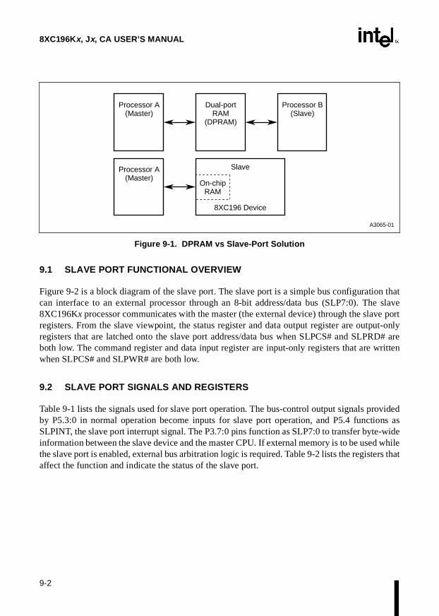
8XC196Kx, Jx, CA USER’S MANUAL
9-2
Figure 9-1. DPRAM vs Slave-Port Solution
9.1 SLAVE PORT FUNCTIONAL OVERVIEW
Figure 9-2 is a block diagram of the slave port. The slave port is a simple bus configuration thatcan interface to an external processor through an 8-bit address/data bus (SLP7:0). The slave8XC196Kx processor communicates with the master (the external device) through the slave portregisters. From the slave viewpoint, the status register and data output register are output-onlyregisters that are latched onto the slave port address/data bus when SLPCS# and SLPRD# areboth low. The command register and data input register are input-only registers that are writtenwhen SLPCS# and SLPWR# are both low.
9.2 SLAVE PORT SIGNALS AND REGISTERS
Table 9-1 lists the signals used for slave port operation. The bus-control output signals providedby P5.3:0 in normal operation become inputs for slave port operation, and P5.4 functions asSLPINT, the slave port interrupt signal. The P3.7:0 pins function as SLP7:0 to transfer byte-wideinformation between the slave device and the master CPU. If external memory is to be used whilethe slave port is enabled, external bus arbitration logic is required. Table 9-2 lists the registers thataffect the function and indicate the status of the slave port.
A3065-01
Processor A (Master)
Processor A (Master)
Dual-port RAM
(DPRAM)
Slave
Processor B (Slave)
On-chip RAM
8XC196 Device

9-3
SLAVE PORT
Figure 9-2. Slave Port Block Diagram
SLP_CON
SLP_ADDR
SLPALE /P5.0
SLP1/P3.1
SLPRD# /P5.3
SLPWR# /P5.2
SLPCS# P5.1
SLP_STAT
P3_REG (Data Out)
P3_PIN (Data In)
SLP_CMD
OE#
OE#
WE#
WE#
Q
Internal Bus
8XC196 Device
D
A0267-03
SLP7:0/ P3.7:0
0
1
SLP_STAT.1
SLP_STAT.0
SLPINT/ P5.4
SLP
_CO
N.1
SLP
_CO
N.0
SLP_CON.2

8XC196Kx, Jx, CA USER’S MANUAL
9-4
Table 9-1. Slave Port Signals
Port PinSlave Port
Signal
Slave Port Signal Type Description
P3.7:0 SLP7:0 I/O Slave Port Address/Data bus
Slave port address/data bus in multiplexed mode and slave port data bus in demultiplexed mode. In multiplexed mode, SLP1 is the source of the internal control signal, SLP_ADDR.
P5.0 SLPALE I Slave Port Address Latch Enable
Functions as either a latch enable input to latch the value on SLP1 (with a multiplexed address/data bus) or as the source of the internal control signal, SLP_ADDR (with a demultiplexed address/data bus).
P5.1 SLPCS# I Slave Port Chip Select
SLPCS# must be held low to enable slave port operation.
P5.2 SLPWR# I Slave Port Write Control Input
This active-low signal is an input to the slave. The rising edge of SLPWR# latches data on port 3 into the P3_PIN or SLP_CMD register.
SLPWR# is multiplexed with P5.2, WR#, and WRL#.
P5.3 SLPRD# I Slave Port Read Control Input
This active-low signal is an input to the slave. Data from the P3_REG or SLP_STAT register is valid after the falling edge of SLPRD#.
P5.4 SLPINT O Slave Port Interrupt
This active-high slave port output signal can be used to interrupt the master processor.
NOTE: SLPINT is multiplexed with P5.4 and the ONCE# func-tion (KR, KQ) or a special test-mode-entry pin (KS, KT).Because driving this pin low on the rising edge ofRESET# could cause the device to enter a reservedtest mode, this pin should not be used as an input.
Table 9-2. Slave Port Control and Status Registers
Mnemonic Address Description
INT_MASK 08H Interrupt Mask
Setting bit 6 enables the output buffer empty (OBE) interrupt; clearing the bit disables it.
Setting bit 7 enables the input buffer full (IBF) interrupt; clearing the bit disables it.
INT_MASK1 13H Interrupt Mask 1
Setting bit 0 enables the command buffer full (CBF) interrupt; clearing the bit disables it.
INT_PEND 09H Interrupt Pending
Bit 6, when set, indicates a pending output buffer empty (OBE) interrupt. This bit is set after the master writes to the data input register, P3_PIN.
Bit 7, when set, indicates a pending input buffer full (IBF). This bit is set after the master reads from the data output register, P3_REG.

9-5
SLAVE PORT
INT_PEND1 12H Interrupt Pending 1
Bit 0, when set, indicates a pending command buffer full (CBF) interrupt. This bit is set after the master writes to the command register, SLP_CMD.
P3_PIN 1FFEH Slave Port Data Input Register
This register is also used for standard port 3 operation.
In slave port operation, this register accepts data written by the master to be read by the slave. The slave can only read from this register and the master can only write to it. If the master attempts to read from P3_PIN, it will actually read P3_REG.
To write to this register in standard slave mode, the master must first write “0” to the pin selected by SLP_CON.2. To write to this register in shared memory mode (8XC196KS and KT only), the master must first write “0” to the SLP1 pin.
P3_REG 1FFCH Slave Port Data Output Register
This register is also used for standard port 3 operation.
In slave port operation, this register accepts data written by the slave to be read by the master. The slave can write to and read from this register. The master can only read it. If the master attempts to write to this register, it will actually write to P3_PIN.
To read from this register in standard slave mode, the master must first write “0” to the pin selected by SLP_CON.2. To read from this register in shared memory mode (8XC196KS and KT only), the master must first write “0” to the SLP1 pin.
SLP_CMD 1FFAH Slave Port Command Register
This register accepts commands from the master to the slave. The commands are defined by the device software. The slave can read from and write to this register. The master can only write to it.
To write to this register in standard slave mode, the master must first write “1” to the pin selected by SLP_CON.2. To write to this register in shared memory mode (8XC196KS and KT only), the master must first write “1” to the SLP1 pin.
SLP_CON 1FFBH Slave Port Control Register
This register is used to configure the slave port. It selects the operating mode (8XC196KS and KT only), enables and disables slave port operation, controls whether the master accesses the data registers or the control and status registers, and controls whether the SLPINT signal is asserted when the input buffer empty (IBE) and output buffer full (OBF) flags are set in the SLP_STAT register. Only the slave can access this register.
SLP_STAT 1FF8H Slave Port Status Register
The master can read this register to determine the status of the slave.
The slave can read all bits. If the master attempts to write to SLP_STAT, it actually writes to SLP_CMD. To read from this register in standard slave mode, the master must first write “1” to the pin selected by SLP_CON.2. To read from this register in shared memory mode (8XC196KS and KT only), the master must first write “1” to the SLP1 pin.
Table 9-2. Slave Port Control and Status Registers (Continued)
Mnemonic Address Description

8XC196Kx, Jx, CA USER’S MANUAL
9-6
9.3 HARDWARE CONNECTIONS
Figure 9-3 shows the basic hardware connections for both multiplexed and demultiplexed busmodes. Table 9-3 lists the interconnections. Note that the shared memory mode (8XC196KS andKT only) supports only a multiplexed bus, while the standard slave mode supports either a mul-tiplexed or a demultiplexed bus.
When using a multiplexed bus, connect the master’s AD1 pin to the slave’s SLP1 pin and the mas-ter’s ALE pin to the slave’s P5.0 pin. When using a demultiplexed bus, connect the master’s ad-dress output (A1) to the slave’s SLPALE (P5.0) pin. The master’s AD1 (with a multiplexed bus)or A1 (with a demultiplexed bus) signal must be held high to either write to the slave’s commandregister (SLP_CMD) or read the slave’s status register (SLP_STAT). It must be held low to eitherwrite to the slave’s P3_PIN register or read the slave’s P3_REG register.
The configurations shown in Figure 9-3 allow the master to select the slave device by forcingSLPCS# low. The master can then request that the slave perform a read or a write operation byforcing SLPRD# or SLPWR# low, respectively. Data is latched on the rising edge of eitherSLPRD# or SLPWR#. When the slave completes a read or a write, it notifies the master via theSLPINT signal.
When the master writes to the P3_PIN register, the input buffer empty (IBE) flag is cleared andSLPINT is pulled low. When the slave reads P3_PIN, the IBE flag is set and SLPINT is forcedhigh. This notifies the master that the write operation is completed and another write can be per-formed.
When the slave writes to P3_REG, the output buffer full (OBF) flag is set and SLPINT is forcedhigh. This notifies the master that P3_REG contains valid data from the previous read cycle. Notethat this is a pipelined read. The address specified in the previous read cycle is fetched and placedinto the P3_REG register to be read by the master in the next read cycle. When the master readsfrom P3_REG, the OBF flag is cleared and SLPINT is pulled low.
Table 9-3. Master and Slave Interconnections
Multiplexed Bus Demultiplexed Bus
Master Slave Master Slave
AD7:0 SLP7:0 D7:0 SLP7:0
ALE SLPALE A1 SLPALE
RD# SLPRD# RD# SLPRD#
WR# SLPWR# WR# SLPWR#
Latched addr. or port pin SLPCS# Latched addr. pin SLPCS#
Interrupt input or port pin SLPINT Interrupt input or port pin SLPINT

9-7
SLAVE PORT
Figure 9-3. Master/Slave Hardware Connections
SLP7:0
SLPALE
SLPRD#
SLPWR#
SLPCS#
SLPINT
8XC196Slave Processor
Address/Data Bus
Address Latch Enable (ALE)
Data Read (RD#)
Data Write (WR#)
Chip Select (CS#)
Slave Interrupt Output
Master Processor
or System Bus
Slave Port Connections for Multiplexed Bus Interface
LELatchedAddressDecoder
SLP7:0
SLPALE
SLPRD#
SLPWR#
SLPCS#
SLPINT
8XC196Slave Processor
Data Bus
System Address Line A1
Data Read (RD#)
Data Write (WR#)
Chip Select (CS#)
Slave Interrupt Output
Master Processor
or System Bus
Slave Port Connections for Demultiplexed Bus Interface
AddressDecoder
Address Bus
A0309-02

8XC196Kx, Jx, CA USER’S MANUAL
9-8
9.4 SLAVE PORT MODES
The slave port can operate in either standard slave mode or shared memory mode (8XC196KSand KT only). In both modes, the master and slave share a 256-byte block of memory located any-where within the slave’s memory space. Data written is stored in the slave’s P3_PIN register; datato be read is stored in the slave’s P3_REG register. The standard slave mode supports either a de-multiplexed or a multiplexed bus and uses the command buffer full (CBF) interrupt. The sharedmemory mode supports only a multiplexed bus and uses the input buffer empty (IBE) and outputbuffer full (OBF) interrupts. In both modes, the interrupts must be processed by a software inter-rupt service routine.
9.4.1 Standard Slave Mode Example
In standard slave mode, the master and slave share a 256-byte block of memory. The high byte ofthe address (the base address) selects the location within the slave’s memory space. The masterwrites the low byte of the address to the slave’s command register (SLP_CMD). This mode canbe used with either a multiplexed or a demultiplexed bus.
In this example, the master and slave share a 256-byte block of memory from 0400–04FFH. Themaster device has arbitrary external memory locations that are dedicated to slave port accesses.
9.4.1.1 Master Device Program
The following code segment illustrates the simple method for writing to the slave.
EXT_P3_PIN EQU 0FFFDH ; (A1=0)EXT_SLP_CMD EQU 0FFFEH ; (A1=1)
STB DATA, EXT_P3_PIN ; write the data into the slave’s P3_PINSTB ADDR, EXT_SLP_CMD ; write address LSB into slave’s SLP_CMD
; wait for SLPINT to go high
The master first writes data to the P3_PIN register, which clears the IBE flag in the slave’sSLP_STAT register and pulls SLPINT low. This notifies the slave to perform a data write at theaddress BASE + SLP_CMD.
The following code segment illustrates the equally simple method for reading from the slave.
EXT_P3_REG EQU 0FFFCH ; (A1=0)EXT_SLP_CMD EQU 0FFFEH ; (A1=1)
LDB TEMP, EXT_P3_REG ; clear slave’s P3_REGSTB ADDR, EXT_SLP_CMD ; write address LSB into slave’s SLP_CMD
; ... wait for SLPINT to go highLDB DATA, EXT_P3_REG ; read the data from P3_REG
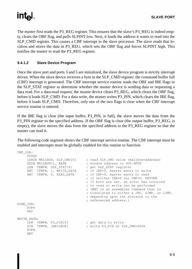
9-9
SLAVE PORT
The master first reads the P3_REG register. This ensures that the slave’s P3_REG is indeed emp-ty, clears the OBF flag, and pulls SLPINT low. Next, it loads the address it wants to read into theSLP_CMD register. This causes a CBF interrupt in the slave processor. The slave reads that lo-cation and stores the data in P3_REG, which sets the OBF flag and forces SLPINT high. Thisnotifies the master to read the P3_REG register.
9.4.1.2 Slave Device Program
Once the slave port and ports 3 and 5 are initialized, the slave device program is strictly interruptdriven. When the slave device receives a byte in the SLP_CMD register, the command buffer full(CBF) interrupt is generated. The CBF interrupt service routine reads the OBF and IBE flags inthe SLP_STAT register to determine whether the master device is sending data or requesting adata read. For a data-read request, the master device clears P3_REG, which clears the OBF flag,before it loads SLP_CMD. For a data write, the master writes P3_PIN, which clears the IBE flag,before it loads SLP_CMD. Therefore, only one of the two flags is clear when the CBF interruptservice routine is entered.
If the IBE flag is clear (the input buffer, P3_PIN, is full), the slave moves the data from theP3_PIN register to the specified address. If the OBF flag is clear (the output buffer, P3_REG, isempty), the slave moves the data from the specified address to the P3_REG register so that themaster can read it.
The following code segment shows the CBF interrupt service routine. The CBF interrupt must beenabled and interrupts must be globally enabled for this routine to function.
CBF_ISR: PUSHA LDBZE MAILBOX, SLP_CMD[0] ; read SLP_CMD value (mailbox=address) ADDB MAILBOX+1, BASE ; window address is 400-4FFH LDB TEMPW, SLP_STAT[0] ; get SLP_STAT register BBC TEMPW, 1, WRITE_DATA ; if IBE=0, master wants to writeBBC TEMPW, 0, READ_DATA ; if OBF=0, master wants to read
; if neither IBE=0 nor OBF=0, RETURN; if both are set, an error has occurred; no read or write can be performed; (BBC is an assembler command that is; translated to either a JBC, SJMP, or LJMP,; depending upon the distance to the ; referenced address.)
DONE_ISR: POPARET
WRITE_DATA: LDB TEMPW, P3_PIN[0] ; get data to writeSTB TEMPW, [MAILBOX] ; write P3_PIN at SLP_CMD+400H POPA RET

8XC196Kx, Jx, CA USER’S MANUAL
9-10
READ_DATA: LDB TEMPW, [MAILBOX] ; get data to write to P3_REG STB TEMPW, P3_REG[0] ; write SLP_CMD+400H data to P3_REG POPA RET
END
9.4.1.3 Demultiplexed Bus Timings
The master processor performs two bus cycles for each byte written and three bus cycles for eachbyte read. For the slave device, only five bytes are used (two bytes for the pointer to the openmemory window, two bytes for the temporary storage register, and one byte for the base address).A read requires 91 state times (11.375 µs at 16 MHz) and a write requires 86 state times (10.750µs at 16 MHz). These times do not include interrupt latency (see “Interrupt Latency” on page5-7). Figure 9-4 shows relative timing relationships. Consult the datasheet for actual timing spec-ifications.
Figure 9-4. Standard Slave Mode Timings (Dem ulti plexed Bus)
Data
SLPCS#
SLPALE (Note 1)
SLPRD#
SLP7:0/ P3.7:0
SLPWR#
SLPINT
A0307-02
Notes: 1. Connect to master's A1 signal. 2. Rising edge associated with either – Read ready (write to P3_REG) – Write complete (read of P3_PIN)
(Note 2)

9-11
SLAVE PORT
9.4.2 Shared Memory Mode Example (8XC196KS and KT only)
In shared memory mode, the master and slave share a 256-byte block of memory. The high byteof the address (the base address) controls the location within the slave device memory space. Thelow byte of the address is always in the SLP_CMD register. The P3_REG register contains datato be read; the P3_PIN register contains the data written. This mode requires a multiplexed bus.
The primary difference between this mode and the standard slave mode is in the way that the ad-dress is loaded into the SLP_CMD register. The low byte of the address is automatically loadedinto SLP_CMD on the falling edge of SLPALE. The data is latched on the rising edge of SLPRD#or SLPWR#. For this reason, a write or read operation requires only one master bus cycle ratherthan two and three bus cycles, respectively, in standard slave mode.
The time between the falling edge of SLPALE and the rising edge of SLPRD# is too short to allowthe slave processor to perform the read. Therefore, reads are pipelined in this mode, as they arein standard slave mode. When the master requests a read operation, the data present during thecurrent bus cycle is either “dummy” data or the data from the previous read operation. Althoughread operations are pipelined, write operations are not. Therefore, write operations can be per-formed between reads without corrupting data that is waiting to be read. This allows the masterto assign higher priority to write cycles. The master must wait for SLPINT to go high betweenreads or writes.
In this example, the master and slave share a 256-byte block of memory from 0400–04FFH.
9.4.2.1 Master Device Program
In this mode, the master simply requests a read and receives data one bus cycle following the pre-vious read. The following code segment illustrates how this is done.
OFFSET EQU 0FF00HADD ADDR,#OFFSET ; point to the external addressLDB DATA,[ADDR] ; read the slave device data
The data that is read is actually the data from the previous read cycle. The address driven causesthe slave to perform an interrupt service routine to fetch the data at that address. The data at theaddress is valid on the rising edge of SLPINT. Writing to the slave is equally simple, as the fol-lowing code segment illustrates.
OFFSET EQU 0FF00HADD ADDR,#OFFSET ; point to the slave addressSTB DATA,[ADDR] ; store data at the address

8XC196Kx, Jx, CA USER’S MANUAL
9-12
9.4.2.2 Slave Device Program
This example shows how the slave device reacts to reads and writes requested by the master. Re-gardless of the operation to be performed, the address is latched into the SLP_CMD register. Theinterrupt determines whether a read or write operation is to be performed.
An IBF interrupt requires a write operation. The slave branches to the IBF interrupt service rou-tine, reads the data in the P3_PIN register, and writes that data to the address specified by addinga base address to the value in SLP_CMD. When the slave reads P3_PIN, it forces SLPINT high,which notifies the master that another operation can be performed.
An OBE interrupt requires a read operation. The slave branches to the OBE interrupt service rou-tine, reads the data at the address specified by adding a base address to the value in SLP_CMD,and writes that data into the P3_REG register. When the slave writes the P3_REG register, it forc-es SLPINT high, which notifies the master that another operation can be performed. (Rememberthat read operations are pipelined.)
The following code segment shows the IBF and OBE interrupt service routines. The interrupt ser-vice routines are very much alike. One reads from the SFR space to the memory block; the otherreads from the memory block to the SFR space. The slave need only know which routine to exe-cute. The IBF and OBE interrupts must be enabled and interrupts must be globally enabled forthese routines to function.
IBF_ISR: PUSHA ; save flagsLDBZE ADDR, SLP_CMD[0] ; load SLP_CMD value into Addr registerADDB ADDR+1, BASE ; add a base to address (16-bit address)LDB TEMP, P3_PIN[0] ; read P3_PIN (read forces SLPINT high)STB TEMP, [ADDR] ; write data to addressPOPARET
OBE_ISR:PUSHA ; save flagsLDBZE ADDR, SLP_CMD[0] ; load SLP_CMD value into Addr registerADDB ADDR+1, BASE ; add a base to address (16-bit address)LDB TEMP, [ADDR] ; load data from address to temp registerSTB TEMP, P3_REG[0] ; write data to P3_REG
; (write forces SLPINT high)POPARET
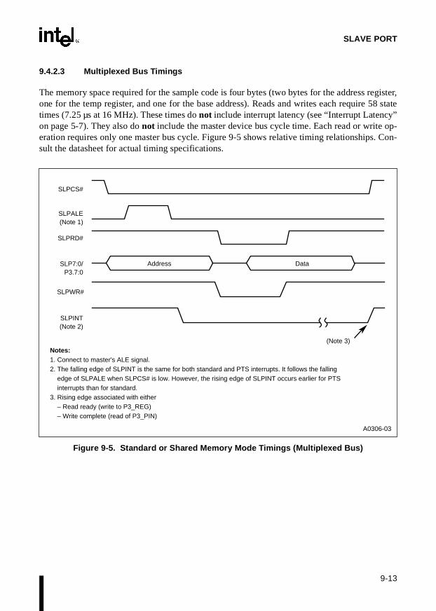
9-13
SLAVE PORT
9.4.2.3 Multiplexed Bus Timings
The memory space required for the sample code is four bytes (two bytes for the address register,one for the temp register, and one for the base address). Reads and writes each require 58 statetimes (7.25 µs at 16 MHz). These times do not include interrupt latency (see “Interrupt Latency”on page 5-7). They also do not include the master device bus cycle time. Each read or write op-eration requires only one master bus cycle. Figure 9-5 shows relative timing relationships. Con-sult the datasheet for actual timing specifications.
Figure 9-5. Sta ndard or Shared Memory Mode Timings (Multiplexed Bus)
A0306-03
SLPCS#
SLPALE (Note 1)
SLPRD#
SLP7:0/ P3.7:0
SLPWR#
SLPINT (Note 2)
Notes: 1. Connect to master's ALE signal. 2. The falling edge of SLPINT is the same for both standard and PTS interrupts. It follows the falling edge of SLPALE when SLPCS# is low. However, the rising edge of SLPINT occurs earlier for PTS interrupts than for standard. 3. Rising edge associated with either – Read ready (write to P3_REG) – Write complete (read of P3_PIN)
DataAddress
(Note 3)

8XC196Kx, Jx, CA USER’S MANUAL
9-14
9.5 CONFIGURING THE SLAVE PORT
Before you can use the slave port, you must configure the associated port 3 and port 5 pins toserve as special-function signals. (See Chapter 6, “I/O Ports,” for configuration details.)
• Configure P5.3:0 as special-function inputs.
• Configure P5.4 as a special-function open-drain or complementary output.
• Configure P3.7:0 as special-function open-drain input/outputs.
The following code example shows the port 5 configuration code.
LDB TEMP, #EFHSTB TEMP, P5_DIR[0] ; make P5.4/SLPINT a complementary output
; set up all other port 5 pins as inputsLDB TEMP, #1FHSTB TEMP, P5_MODE[0] ; select special function for P5.4:0LDB TEMP, #FFHSTB TEMP, P5_REG[0] ; write all ones to P5_REG
The following code example shows the port 3 configuration code.
LDB TEMP, P34_DRV[0] ; read the current state of P34_DRVANDB TEMP, #7FH ; clear the MSB of P34_DRVSTB TEMP, P34_DRV[0] ; make Port 3 open-drain
Once you have configured the pins, you must initialize the registers. This example shows the ini-tialization code. The remaining sections of this chapter describe the registers and explain the con-figuration options.
LDB TEMP, #slave_mode ; 0FH for standard, 1BH for shared mem modeSTB TEMP, SLP_CON[0] ; initialize the slave port STB ONES_REG, P3_REG[0] ; write all ones to port 3 (write sets OBF)STB ZERO_REG, SLP_CMD[0] ; clear the command registerSTB ZERO_REG, P3_PIN[0] ; clear the data input registerLDB TEMP, SLP_STAT[0] ; read the status reg (CBE, IBE, OBF=111)
9.5.1 Programming the Slave Port Control Register (SLP_CON)
The SLP_CON register (Figure 9-6) selects the operating mode, enables and disables slave portoperation, controls whether the master accesses the data registers or the control and status regis-ters, and controls whether the SLPINT signal is asserted when the input buffer empty (IBE) andoutput buffer full (OBF) flags are set in the SLP_STAT register. Only the slave can access thisregister.
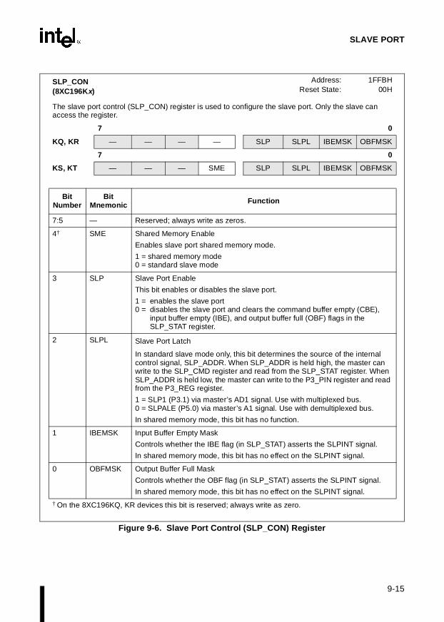
9-15
SLAVE PORT
SLP_CON(8XC196Kx)
Address:Reset State:
1FFBH00H
The slave port control (SLP_CON) register is used to configure the slave port. Only the slave can access the register.
7 0
KQ, KR — — — — SLP SLPL IBEMSK OBFMSK
7 0
KS, KT — — — SME SLP SLPL IBEMSK OBFMSK
BitNumber
BitMnemonic Function
7:5 — Reserved; always write as zeros.
4† SME Shared Memory Enable
Enables slave port shared memory mode.
1 = shared memory mode0 = standard slave mode
3 SLP Slave Port Enable
This bit enables or disables the slave port.
1 = enables the slave port0 = disables the slave port and clears the command buffer empty (CBE),
input buffer empty (IBE), and output buffer full (OBF) flags in the SLP_STAT register.
2 SLPL Slave Port Latch
In standard slave mode only, this bit determines the source of the internal control signal, SLP_ADDR. When SLP_ADDR is held high, the master can write to the SLP_CMD register and read from the SLP_STAT register. When SLP_ADDR is held low, the master can write to the P3_PIN register and read from the P3_REG register.
1 = SLP1 (P3.1) via master’s AD1 signal. Use with multiplexed bus.0 = SLPALE (P5.0) via master’s A1 signal. Use with demultiplexed bus.
In shared memory mode, this bit has no function.
1 IBEMSK Input Buffer Empty Mask
Controls whether the IBE flag (in SLP_STAT) asserts the SLPINT signal.
In shared memory mode, this bit has no effect on the SLPINT signal.
0 OBFMSK Output Buffer Full Mask
Controls whether the OBF flag (in SLP_STAT) asserts the SLPINT signal.
In shared memory mode, this bit has no effect on the SLPINT signal.
† On the 8XC196KQ, KR devices this bit is reserved; always write as zero.
Figure 9-6. Slave Port Control (SLP_CON) Register

8XC196Kx, Jx, CA USER’S MANUAL
9-16
9.5.2 Enabling the Slave Port Interrupts
The master can generate three interrupt requests: command buffer full (CBF), output buffer emp-ty (OBE), and input buffer full (IBF). The CBF interrupt is used in standard slave mode; the OBEand IBF interrupts are used in shared memory mode. To enable an interrupt, set the correspondingbit in the interrupt mask register (Table 9-2 on page 9-4).
9.6 DETERMINING SLAVE PORT STATUS
The master can determine the status of the slave port by reading the SLP_STAT register (Figure9-7). It can also read the interrupt pending registers (Table 9-2 on page 9-4) to determine the statusof the interrupts.
9.7 USING STATUS BITS TO SYNCHRONIZE MASTER AND SLAVE
The status bits in the SLP_STAT register can be used to synchronize the master with the slave.Because synchronization of the status bits is not monitored by the status flags, it is more difficultfor the master to monitor. Software must ensure data integrity throughout the operation. Twotechniques are recommended — a double read or a software flag.
If the master processor is fast enough to read SLP_STAT twice before the contents change, themaster can compare the readings from before and after the data fetch. If the readings are identical,the data is guaranteed correct.
In standard slave mode, the slave can use bit 7 of SLP_STAT to indicate valid data. To update thestatus, the slave performs the following sequence:
• Clear the flag bit (bit 7) without changing the other four status bits.
• Update the status bits (SLP_STAT.6:3).
• Set the flag bit (bit 7) without changing the other four status bits.
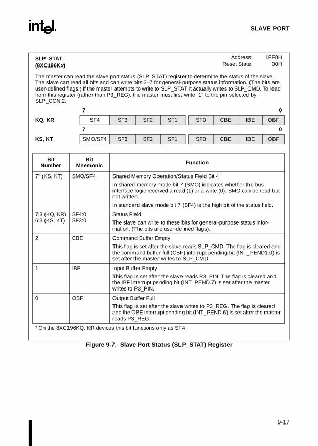
9-17
SLAVE PORT
SLP_STAT(8XC196Kx)
Address:Reset State:
1FF8H00H
The master can read the slave port status (SLP_STAT) register to determine the status of the slave. The slave can read all bits and can write bits 3–7 for general-purpose status information. (The bits are user-defined flags.) If the master attempts to write to SLP_STAT, it actually writes to SLP_CMD. To read from this register (rather than P3_REG), the master must first write “1” to the pin selected by SLP_CON.2.
7 0
KQ, KR SF4 SF3 SF2 SF1 SF0 CBE IBE OBF
7 0
KS, KT SMO/SF4 SF3 SF2 SF1 SF0 CBE IBE OBF
BitNumber
BitMnemonic Function
7† (KS, KT) SMO/SF4 Shared Memory Operation/Status Field Bit 4
In shared memory mode bit 7 (SMO) indicates whether the bus interface logic received a read (1) or a write (0). SMO can be read but not written.
In standard slave mode bit 7 (SF4) is the high bit of the status field.
7:3 (KQ, KR)6:3 (KS, KT)
SF4:0SF3:0
Status Field
The slave can write to these bits for general-purpose status infor-mation. (The bits are user-defined flags).
2 CBE Command Buffer Empty
This flag is set after the slave reads SLP_CMD. The flag is cleared and the command buffer full (CBF) interrupt pending bit (INT_PEND1.0) is set after the master writes to SLP_CMD.
1 IBE Input Buffer Empty
This flag is set after the slave reads P3_PIN. The flag is cleared and the IBF interrupt pending bit (INT_PEND.7) is set after the master writes to P3_PIN.
0 OBF Output Buffer Full
This flag is set after the slave writes to P3_REG. The flag is cleared and the OBE interrupt pending bit (INT_PEND.6) is set after the master reads P3_REG.
† On the 8XC196KQ, KR devices this bit functions only as SF4.
Figure 9-7. Slave Port Status (SLP_STAT) Register

10Event Processor Array (EPA)


10-1
CHAPTER 10EVENT PROCESSOR ARRAY (EPA)
Control applications often require high-speed event control. For example, the controller may needto periodically generate pulse-width modulated outputs, an analog-to-digital conversion, or an in-terrupt. In another application, the controller may monitor an input signal to determine the statusof an external device. The event processor array (EPA) was designed to reduce the CPU overheadassociated with these types of event control. This chapter describes the EPA and its timers andexplains how to configure and program them.
10.1 EPA FUNCTIONAL OVERVIEW
The EPA performs input and output functions associated with two timer/counters, timer 1 andtimer 2 (Figure 10-1). In the input mode, the EPA monitors an input pin for an event: a rising edge,a falling edge, or an edge in either direction. When the event occurs, the EPA records the valueof the timer/counter, so that the event is tagged with a time. This is called an input capture. Inputcaptures are buffered to allow two captures before an overrun occurs. In the output mode, the EPAmonitors a timer/counter and compares its value with a value stored in a register. When the tim-er/counter value matches the stored value, the EPA can trigger an event: a timer reset or an outputevent (set a pin, clear a pin, toggle a pin, or take no action). This is called an output compare. TheEPA sets an interrupt pending bit in response to an input capture or an output compare. This bitcan optionally cause an interrupt. Table 10-1 lists the capture/compare and compare-only chan-nels for each device in the 8XC196Kx family.
Table 10-1. EPA Channels
Device Capture/Compare Channels Compare-only Channels
87C196CA, 8XC196Jx EPA3:0 & EPA9:8 COMP1:0
8XC196Kx EPA9:0 COMP1:0
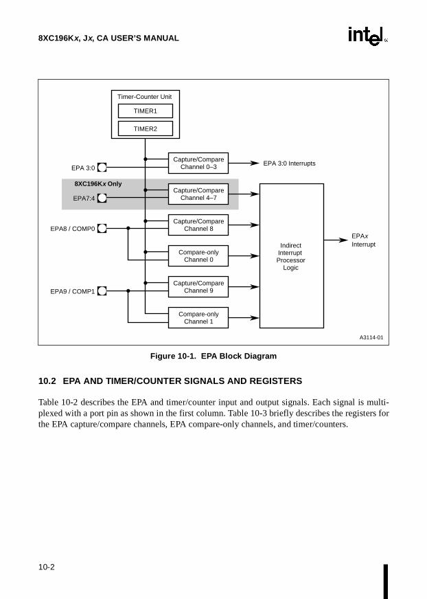
8XC196Kx, Jx, CA USER’S MANUAL
10-2
Figure 10-1. EPA Block Diagram
10.2 EPA AND TIMER/COUNTER SIGNALS AND REGISTERS
Table 10-2 describes the EPA and timer/counter input and output signals. Each signal is multi-plexed with a port pin as shown in the first column. Table 10-3 briefly describes the registers forthe EPA capture/compare channels, EPA compare-only channels, and timer/counters.
Indirect Interrupt Processor
Logic
EPAx Interrupt
A3114-01
TIMER1
TIMER2
Timer-Counter Unit
Compare-only Channel 1
Capture/Compare Channel 9
Compare-only Channel 0
Capture/Compare Channel 8
Capture/Compare Channel 4–7
Capture/Compare Channel 0–3
EPA9 / COMP1
EPA8 / COMP0
EPA7:4
EPA 3:0
8XC196Kx Only
EPA 3:0 Interrupts
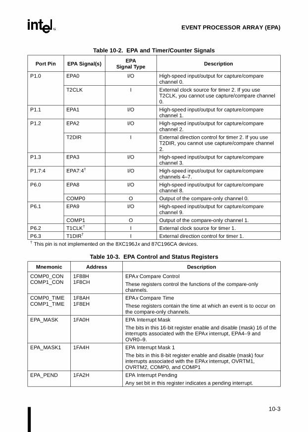
10-3
EVENT PROCESSOR ARRAY (EPA)
Table 10-2. EPA and Timer/Counter Signals
Port Pin EPA Signal(s) EPASignal Type Description
P1.0 EPA0 I/O High-speed input/output for capture/compare channel 0.
T2CLK I External clock source for timer 2. If you use T2CLK, you cannot use capture/compare channel 0.
P1.1 EPA1 I/O High-speed input/output for capture/compare channel 1.
P1.2 EPA2 I/O High-speed input/output for capture/compare channel 2.
T2DIR I External direction control for timer 2. If you use T2DIR, you cannot use capture/compare channel 2.
P1.3 EPA3 I/O High-speed input/output for capture/compare channel 3.
P1.7:4 EPA7:4† I/O High-speed input/output for capture/compare channels 4–7.
P6.0 EPA8 I/O High-speed input/output for capture/compare channel 8.
COMP0 O Output of the compare-only channel 0.
P6.1 EPA9 I/O High-speed input/output for capture/compare channel 9.
COMP1 O Output of the compare-only channel 1.
P6.2 T1CLK† I External clock source for timer 1.
P6.3 T1DIR† I External direction control for timer 1.† This pin is not implemented on the 8XC196Jx and 87C196CA devices.
Table 10-3. EPA Control and Status Registers
Mnemonic Address Description
COMP0_CONCOMP1_CON
1F88H1F8CH
EPAx Compare Control
These registers control the functions of the compare-only channels.
COMP0_TIMECOMP1_TIME
1F8AH1F8EH
EPAx Compare Time
These registers contain the time at which an event is to occur on the compare-only channels.
EPA_MASK 1FA0H EPA Interrupt Mask
The bits in this 16-bit register enable and disable (mask) 16 of the interrupts associated with the EPAx interrupt, EPA4–9 and OVR0–9.
EPA_MASK1 1FA4H EPA Interrupt Mask 1
The bits in this 8-bit register enable and disable (mask) four interrupts associated with the EPAx interrupt, OVRTM1, OVRTM2, COMP0, and COMP1
EPA_PEND 1FA2H EPA Interrupt Pending
Any set bit in this register indicates a pending interrupt.

8XC196Kx, Jx, CA USER’S MANUAL
10-4
EPA_PEND1 1FA6H EPA Interrupt Pending 1
Any set bit in this register indicates a pending interrupt.
EPA0_CONEPA1_CONEPA2_CONEPA3_CONEPA4_CONEPA5_CONEPA6_CONEPA7_CONEPA8_CONEPA9_CON
1F60H1F64H1F68H1F6CH1F70H1F74H1F78H1F7CH1F80H1F84H
EPAx Capture/Compare Control
These registers control the functions of the capture/compare channels. EPA1_CON and EPA3_CON require an extra byte because they contain an additional bit for PWM remap mode. These two registers must be addressed as words; the others can be addressed as bytes.
EPA0_TIMEEPA1_TIMEEPA2_TIMEEPA3_TIMEEPA4_TIMEEPA5_TIMEEPA6_TIMEEPA7_TIMEEPA8_TIMEEPA9_TIME
1F62H1F66H1F6AH1F6EH1F72H1F76H1F7AH1F7EH1F82H1F86H
EPAx Capture/Compare Time
In capture mode, these registers contain the captured timer value. In compare mode, these registers contain the time at which an event is to occur. In capture mode, these registers are buffered to allow two captures before an overrun occurs. However, they are not buffered in compare mode.
EPAIPV 1FA8H EPA Interrupt Priority Vector Register
The lower four bits of this register contain a number from 01H to 14H corresponding to the highest priority active EPAx interrupt source. This value, when used with the TIJMP instruction, enables software to branch to the correct interrupt service routine for the active interrupt.
INT_MASK 0008H Interrupt Mask
Five bits in this register enable and disable (mask) the individual EPA0, EPA1, EPA2, and EPA3 interrupts and the multiplexed EPAx interrupt. The EPA_MASK and EPA_MASK1 register bits enable and disable the individual sources of the EPAx interrupt.
INT_PEND 0009H Interrupt Pending
Five bits in this register are set to indicate pending individual interrupts EPA0, EPA1, EPA2, and EPA3, and the multiplexed EPAx interrupt. The EPA_PEND and EPA_PEND1 register bits indicate which source(s) of the EPAx interrupt are pending.
P1_DIRP6_DIR
1FD2H 1FD3H
Port x Direction
Each bit of Px_DIR controls the direction of the corresponding pin. Clearing a bit configures a pin as a complementary output; setting a bit configures a pin as an input or open-drain output. (Open-drain outputs require external pull-ups.)
P1_MODE P6_MODE
1FD0H1FD1H
Port x Mode
Each bit of Px_MODE controls whether the corresponding pin functions as a standard I/O port pin or as a special-function signal. Setting a bit configures a pin as a special-function signal; clearing a bit configures a pin as a standard I/O port pin.
Table 10-3. EPA Control and Status Registers (Continued)
Mnemonic Address Description

10-5
EVENT PROCESSOR ARRAY (EPA)
P1_PINP6_PIN
1FD6H1FD7H
Port x Input
Each bit of Px_PIN reflects the current state of the corresponding pin, regardless of the pin configuration.
P1_REG P6_REG
1FD4H1FD5H
Port x Data Output
For an input, set the corresponding Px_REG bit.
For an output, write the data to be driven out by each pin to the corresponding bit of Px_REG. When a pin is configured as standard I/O (Px_MODE.x=0), the result of a CPU write to Px_REG is immediately visible on the pin. When a pin is configured as a special-function signal (Px_MODE.x=1), the associated on-chip peripheral or off-chip component controls the pin. The CPU can still write to Px_REG, but the pin is unaffected until it is switched back to its standard I/O function.
This feature allows software to configure a pin as standard I/O (clear Px_MODE.x), initialize or overwrite the pin value, then configure the pin as a special-function signal (set Px_MODE.x). In this way, initialization, fault recovery, exception handling, etc., can be done without changing the operation of the associated peripheral.
T1CONTROL 1F98H Timer 1 Control
This register enables/disables timer 1, controls whether it counts up or down, selects the clock source and direction, and determines the clock prescaler setting.
T2CONTROL 1F9CH Timer 2 Control
This register enables/disables timer 2, controls whether it counts up or down, selects the clock source and direction, and determines the clock prescaler setting.
TIMER1 1F9AH Timer 1 Value
This register contains the current value of timer 1.
TIMER2 1F9EH Timer 2 Value
This register contains the current value of timer 2.
Table 10-3. EPA Control and Status Registers (Continued)
Mnemonic Address Description
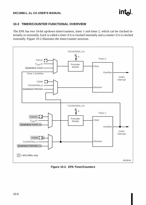
8XC196Kx, Jx, CA USER’S MANUAL
10-6
10.3 TIMER/COUNTER FUNCTIONAL OVERVIEW
The EPA has two 16-bit up/down timer/counters, timer 1 and timer 2, which can be clocked in-ternally or externally. Each is called a timer if it is clocked internally and a counter if it is clockedexternally. Figure 10-2 illustrates the timer/counter structure.
Figure 10-2. EPA Timer/Counters
T2CLK
FOSC/4
Timer 1 Overflow
T2DIR
T2CONTROL.6
Timer 1
T1CLK
FOSC/4Prescaler Module
T1CONTROL.2:0
3
T1CONTROL.6
T1DIR
Overflow
OVR1 Interrupt
A3129-01
Timer 2
ClockPrescaler Module
T2CONTROL.2:0
3
Direction
Overflow
OVR2 Interrupt
Clock
Direction
Quadrature Direction
Quadrature Count
Quadrature Count
Quadrature Direction
= 8XC196Kx only

10-7
EVENT PROCESSOR ARRAY (EPA)
The timer/counters can be used as time bases for input captures, output compares, and pro-grammed interrupts (software timers). When a counter increments from FFFEH to FFFFH or dec-rements from 0001H to 0000H, the counter-overflow interrupt pending bit is set. This bit canoptionally cause an interrupt. The clock source, direction-control source, count direction, and res-olution of the input capture or output compare are all programmable (see “Programming the Tim-ers” on page 10-17). The maximum count rate is one-half the internal clock rate, or FOSC/4 (whereFOSC is the XTAL1 frequency, in Hz). This provides a 250 ns resolution (at 16 MHz) for an inputcapture or output compare.
10.3.1 Cascade Mode (Timer 2 Only)
Timer 2 can be used in cascade mode. In this mode, the timer 1 overflow output is used as thetimer 2 clock input. Either the direction control bit of the timer 2 control register or the directioncontrol assigned to timer 1 controls the count direction. This method, called cascading, can pro-vide a slow clock for idle mode timeout control or for slow pulse-width modulation (PWM) ap-plications (see “Generating a Low-speed PWM Output” on page 10-14).
10.3.2 Quadrature Clocking Mode
On the 8XC196Kx, both timer 1 and timer 2 can be used in quadrature clocking mode. (On the8XC196 Jx and CA, only timer 2 supports quadrature clocking mode.) This mode uses the TxCLKand TxDIR pins as quadrature inputs, as shown in Figure 10-3. External quadrature-encoded sig-nals (two signals at the same frequency that differ in phase by 90°) are input, and the timer incre-ments or decrements by one count on each rising edge and each falling edge. Because the TxCLKand TxDIR inputs are sampled by the internal phase clocks, transitions must be separated by atleast two state times for proper operation. The count is clocked by PH2, which is PH1 delayed byone-half period. The sequence of the signal edges and levels controls the count direction. Referto Figure 10-4 and Table 10-4 for sequencing information.
A typical source of quadrature-encoded signals is a shaft-angle decoder, shown in Figure 10-3.Its output signals X and Y are input to TxCLK and TxDIR, which in turn output signalsX_internal and Y_internal. These signals are used in Figure 10-4 and Table 10-4 to describe thedirection of the shaft.

8XC196Kx, Jx, CA USER’S MANUAL
10-8
Figure 10-3. Quadrature Mode Interface
Table 10-4. Quadrature Mode Truth Table
State of X_internal (TxCLK)
State of Y_internal (TxDIR) Count Direction
↑ 0 Increment
↓ 1 Increment
0 ↓ Increment
1 ↑ Increment
↓ 0 Decrement
↑ 1 Decrement
0 ↑ Decrement
1 ↓ Decrement
Optical Reader TxDIR
TxCLKD Q D Q D Q
D Q D Q D Q
X_internal
Y_internal
PH2
PH1
8XC196 DeviceIncrement
Decrement
X
Y
A0268-02

10-9
EVENT PROCESSOR ARRAY (EPA)
Figure 10-4. Quadrature Mode Timing and Count
10.4 EPA CHANNEL FUNCTIONAL OVERVIEW
The EPA has ten programmable capture/compare channels that can perform the following tasks.
• capture the current timer value when a specified transition occurs on the EPA pin
• start an A/D conversion when an event is captured or the timer value matches theprogrammed value in the event-time register
• clear, set, or toggle the EPA pin when the timer value matches the programmed value in theevent-time register
• generate an interrupt when a capture or compare event occurs
• generate an interrupt when a capture overrun occurs
• reset its own base timer in compare mode
• reset the opposite timer in both compare and capture mode
In addition to the capture/compare channels, the EPA also has two compare-only channels. Theysupport all the compare functions of the capture/compare channels.
TxCLK
TxDIR
COUNT x x + 1 x + 2 x + 3 x + 4 x + 5 x + 6 x + 5 x + 4 x + 3 x + 2 x + 1
A0269-02
PH2
CLKOUT
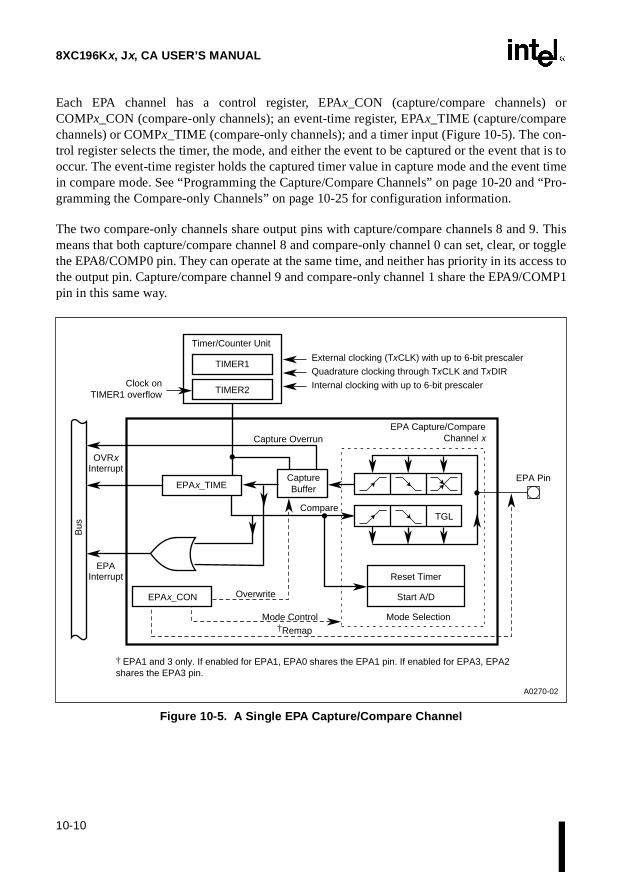
8XC196Kx, Jx, CA USER’S MANUAL
10-10
Each EPA channel has a control register, EPAx_CON (capture/compare channels) orCOMPx_CON (compare-only channels); an event-time register, EPAx_TIME (capture/comparechannels) or COMPx_TIME (compare-only channels); and a timer input (Figure 10-5). The con-trol register selects the timer, the mode, and either the event to be captured or the event that is tooccur. The event-time register holds the captured timer value in capture mode and the event timein compare mode. See “Programming the Capture/Compare Channels” on page 10-20 and “Pro-gramming the Compare-only Channels” on page 10-25 for configuration information.
The two compare-only channels share output pins with capture/compare channels 8 and 9. Thismeans that both capture/compare channel 8 and compare-only channel 0 can set, clear, or togglethe EPA8/COMP0 pin. They can operate at the same time, and neither has priority in its access tothe output pin. Capture/compare channel 9 and compare-only channel 1 share the EPA9/COMP1pin in this same way.
Figure 10-5. A Single EPA Capture/Compare Channel
External clocking (TxCLK) with up to 6-bit prescaler
Quadrature clocking through TxCLK and TxDIR
Internal clocking with up to 6-bit prescalerClock on TIMER1 overflow
TIMER1
TIMER2
EPA Interrupt
EPAx_CON
TGL
Reset Timer
Start A/D
Mode Selection†Remap
EPA PinEPAx_TIME
OVRx Interrupt
A0270-02
Timer/Counter Unit
Capture Buffer
Overwrite
Mode Control
Compare
Capture OverrunEPA Capture/Compare
Channel x
† EPA1 and 3 only. If enabled for EPA1, EPA0 shares the EPA1 pin. If enabled for EPA3, EPA2 shares the EPA3 pin.
Bus
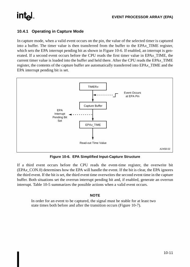
10-11
EVENT PROCESSOR ARRAY (EPA)
10.4.1 Operating in Capture Mode
In capture mode, when a valid event occurs on the pin, the value of the selected timer is capturedinto a buffer. The timer value is then transferred from the buffer to the EPAx_TIME register,which sets the EPA interrupt pending bit as shown in Figure 10-6. If enabled, an interrupt is gen-erated. If a second event occurs before the CPU reads the first timer value in EPAx_TIME, thecurrent timer value is loaded into the buffer and held there. After the CPU reads the EPAx_TIMEregister, the contents of the capture buffer are automatically transferred into EPAx_TIME and theEPA interrupt pending bit is set.
Figure 10-6. EPA Simplified Input-Capture Structure
If a third event occurs before the CPU reads the event-time register, the overwrite bit(EPAx_CON.0) determines how the EPA will handle the event. If the bit is clear, the EPA ignoresthe third event. If the bit is set, the third event time overwrites the second event time in the capturebuffer. Both situations set the overrun interrupt pending bit and, if enabled, generate an overruninterrupt. Table 10-5 summarizes the possible actions when a valid event occurs.
NOTE
In order for an event to be captured, the signal must be stable for at least two state times both before and after the transition occurs (Figure 10-7).
TIMERx
Capture Buffer
EPAx_TIME
Read-out Time Value
EPA Interrupt
Pending Bit Set
Event Occurs at EPA Pin
A2458-02
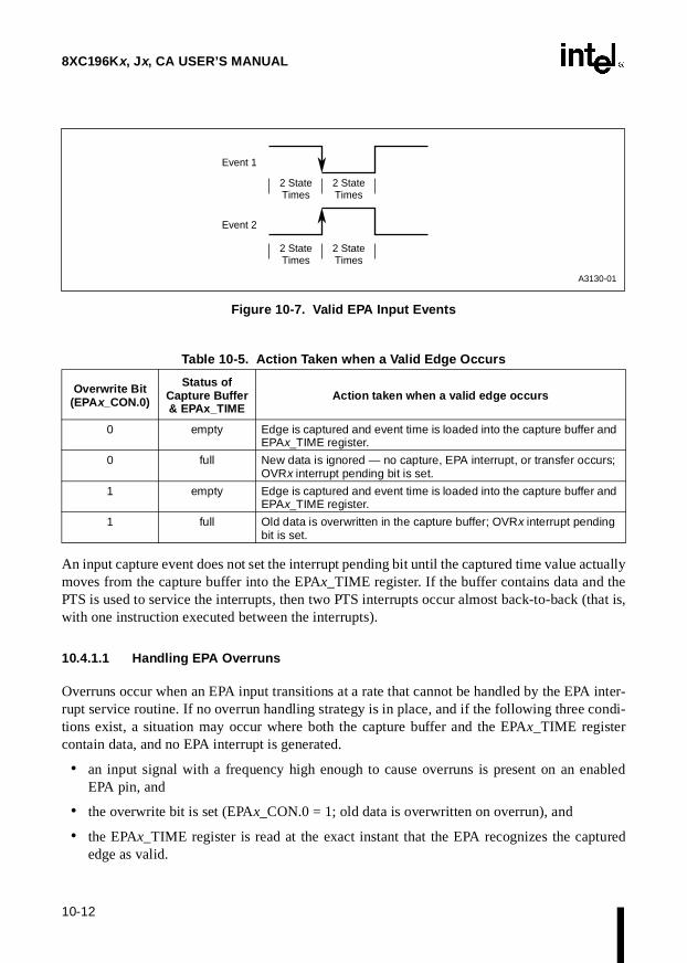
8XC196Kx, Jx, CA USER’S MANUAL
10-12
Figure 10-7. Valid EPA Input Events
An input capture event does not set the interrupt pending bit until the captured time value actuallymoves from the capture buffer into the EPAx_TIME register. If the buffer contains data and thePTS is used to service the interrupts, then two PTS interrupts occur almost back-to-back (that is,with one instruction executed between the interrupts).
10.4.1.1 Handling EPA Overruns
Overruns occur when an EPA input transitions at a rate that cannot be handled by the EPA inter-rupt service routine. If no overrun handling strategy is in place, and if the following three condi-tions exist, a situation may occur where both the capture buffer and the EPAx_TIME registercontain data, and no EPA interrupt is generated.
• an input signal with a frequency high enough to cause overruns is present on an enabledEPA pin, and
• the overwrite bit is set (EPAx_CON.0 = 1; old data is overwritten on overrun), and
• the EPAx_TIME register is read at the exact instant that the EPA recognizes the capturededge as valid.
Table 10-5. Action Taken when a Valid Edge Occurs
Overwrite Bit(EPAx_CON.0)
Status of Capture Buffer& EPAx_TIME
Action taken when a valid edge occurs
0 empty Edge is captured and event time is loaded into the capture buffer and EPAx_TIME register.
0 full New data is ignored — no capture, EPA interrupt, or transfer occurs; OVRx interrupt pending bit is set.
1 empty Edge is captured and event time is loaded into the capture buffer and EPAx_TIME register.
1 full Old data is overwritten in the capture buffer; OVRx interrupt pending bit is set.
A3130-01
Event 1
2 State Times
2 State Times
Event 2
2 State Times
2 State Times

10-13
EVENT PROCESSOR ARRAY (EPA)
The input frequency at which this occurs depends on the length of the interrupt service routine aswell as other factors. Unless the interrupt service routine includes a check for overruns, this situ-ation will remain the same until the device is reset or the EPAx_TIME register is read. The act ofreading EPAx_TIME allows the buffered time value to be moved into EPAx_TIME. This clearsthe buffer and allows another event to be captured. Remember that the act of the transferring thebuffer contents to the EPAx_TIME register is what actually sets the EPAx interrupt pending bitand generates the interrupt.
Any one of the following methods can be used to prevent or recover from this situation.
• Clear EPAx_CON.0
When the overwrite bit (EPAx_CON.0) is zero, the EPA does not consider the capturededge until the EPAx_TIME register is read and the data in the capture buffer is transferred toEPAx_TIME. This prevents the situation by ignoring new input capture events when boththe capture buffer and EPAx_TIME contain valid capture times. The OVRx pending bit inEPA_PEND is set to indicate that an overrun occurred.
• Enable the OVRx interrupt and read the EPAx_TIME register within the ISR
If this situation occurs, the overrun (OVRx) interrupt will be generated. The OVRx interruptwill then be acknowledged and its interrupt service routine will read the EPAx_TIME regis-ter. After the CPU reads the EPAx_TIME register, the buffered data moves from the bufferto the EPAx_TIME register. This sets the EPA interrupt pending bit.
• Check for pending EPAx interrupts before exiting an EPAx ISR
Another method for avoiding this situation is to check for pending EPA interrupts beforeexiting the EPA interrupt service routine. This is an easy way to detect overruns and addi-tional interrupts. It can also save loop time by eliminating the latency necessary to servicethe pending interrupt. However, this method cannot be used with the peripheral transactionserver (PTS). If your system uses the PTS, you should choose one of the other methods.
10.4.2 Operating in Compare Mode
When the selected timer value matches the event-time value, the action specified in the controlregister occurs (i.e., the pin is set, cleared, toggled, or an A/D conversion is initiated). If the re-enable bit (EPAx_CON.3 or COMPx_CON.3) is set, the action reoccurs on every timer match. Ifthe re-enable bit is cleared, the action does not reoccur until a new value is written to the event-time register. See “Programming the Capture/Compare Channels” on page 10-20 and “Program-ming the Compare-only Channels” on page 10-25 for configuration information.
In compare mode, you can use the EPA to produce a pulse-width modulated (PWM) output. Thefollowing sections describe four possible methods.

8XC196Kx, Jx, CA USER’S MANUAL
10-14
10.4.2.1 Generating a Low-speed PWM Output
You can generate a low-speed, pulse-width modulated output with a single EPA channel and astandard interrupt service routine. Configure the EPA channel as follows: compare mode, toggleoutput, and the compare function re-enabled. Select standard interrupt service, enable the EPAinterrupt, and globally enable interrupts with the EI instruction. When the assigned timer/countervalue matches the value in the event-time register, the EPA toggles the output pin and generatesan interrupt. The interrupt service routine loads a new value into EPAx_TIME.
The maximum output frequency depends upon the total interrupt latency and the interrupt-serviceexecution times used by your system. As additional EPA channels and the other functions of themicrocontroller are used, the maximum PWM frequency decreases because the total interrupt la-tency and interrupt-service execution time increases. To determine the maximum, low-speedPWM frequency in your system, calculate your system's worst-case interrupt latency and worst-case interrupt-service execution time, and then add them together. The worst-case interrupt la-tency is the total latency of all the interrupts (both normal and PTS) used in your system. Theworst-case interrupt-service execution time is the total execution time of all interrupt service rou-tines and PTS routines.
The following example shows the calculations for a system that uses a single EPA channel, a sin-gle enabled interrupt, and the following interrupt service routine.
;If EPA0-3 interrupt is generatedEPA0-3_ISR:
PUSHALD EPAx_CON, #toggle_commandADD EPAx_TIME, TIMER x, [next_duty_ptr]; Load next event timePOPARET
;If EPA x interrupt is generated from EPA4-9 interruptsEPAx_ISR:
PUSHALD jtbase_ptr, #LSW jtbase1LD epaipv_ptr, EPAIPV ; Load contents of EPAIPV reg into ptrTIJMP jtbase_ptr,[epaipv_ptr],7FH ; Jump to appropriate EPA ISR
;EPA4-9 service routinesEPA4-9_ISR:
PUSHALD EPAx_CON, #toggle_commandADD EPAx_TIME,TIMER x,[next_duty_ptr]LJMP EPAx_DONE
EPAx_DONE:POPARET

10-15
EVENT PROCESSOR ARRAY (EPA)
The worst-case interrupt latency for a single-interrupt system is 56 state times for external stackusage and 54 state times for internal stack usage (see “Standard Interrupt Latency” on page 5-9).To determine the execution time for an interrupt service routine, add up the execution time of theinstructions in the ISR (Table A-9).
The total execution time for the ISR that services interrupts EPA3:0 is 79 state times for externalstack usage or 71 state times for internal stack usage. Therefore, a single capture/compare channel0–3 can be updated every 125 state times assuming internal stack usage (54 + 71). Each PWMperiod requires two updates (one setting and one clearing), so the execution time for a PWM pe-riod equals 250 state times. At 16 MHz, the PWM period is 31.25 µs and the maximum PWMfrequency is 32 kHz.
The total execution time for the ISR that services the EPAx (capture/compare channels 4–9) in-terrupt is 175 state times for external stack usage or 159 for internal stack usage. Therefore, a sin-gle capture/compare channel 4–7 can be updated every 213 state times assuming internal stackusage (54 + 159). Each PWM period requires two updates (one setting and one clearing), so theexecution time for a PWM period equals 426 state times. At 16 MHz, the PWM period is53.25 µs and the maximum PWM frequency is 18.8 kHz.
10.4.2.2 Generating a Medium-speed PWM Output
You can generate a medium-speed, pulse-width modulated output with a single EPA channel andthe PTS set up in PWM toggle mode. “PWM Toggle Mode Example” on page 5-32 describes howto configure the EPA and PTS. Once started, this method requires no CPU intervention unless youneed to change the output frequency. The method uses a single timer/counter. The timer/counteris not interrupted during this process, so other EPA channels can also use it if they do not reset it.
The maximum output frequency depends upon the total interrupt latency and interrupt-service ex-ecution time. As additional EPA channels and the other functions of the microcontroller are used,the maximum PWM frequency decreases because the total interrupt latency and interrupt-serviceexecution time increases. To determine the maximum, medium-speed PWM frequency in yoursystem, calculate your system's worst-case interrupt latency and worst-case interrupt-service ex-ecution time, and then add them together. The worst-case interrupt latency is the total latency ofall the interrupts (both normal and PTS) used in your system. The worst-case interrupt-serviceexecution time is the total execution time of all interrupt service routines and PTS cycles.
The following example shows the calculations for a system that uses a single EPA channel, a sin-gle enabled interrupt, and PTS service. This example assumes that the PTS has been initialized,the duty cycle and frequency are fixed, and that the interrupt from the capture/compare channelis not multiplexed (i.e., EPA3:0).

8XC196Kx, Jx, CA USER’S MANUAL
10-16
The worst-case interrupt latency for a single-interrupt system with PTS service is 43 state times(see “PTS Interrupt Latency” on page 5-10). The PTS cycle execution time in PWM toggle modeis 15 state times (Table 5-4 on page 5-10). Therefore, a single capture/compare channel 0–3 canbe updated every 58 state times (43 + 15). Each PWM period requires two updates (one settingand one clearing), so the execution time for a PWM period equals 116 state times. At 16 MHz,the PWM period is 14.49 µs and the maximum PWM frequency is 68.97 kHz.
10.4.2.3 Generating a High-speed PWM Output
You can generate a high-speed, pulse-width modulated output with a pair of EPA channels andthe PTS set up in PWM remap mode. “PWM Remap Mode Example” on page 5-37 describes howto configure the EPA and PTS. The remap bit (bit 8) must be set in EPA1_CON (to pair EPA0 andEPA1) or EPA3_CON (to pair EPA2 and EPA3). One channel must be configured to set the out-put; the other, to clear it. At the set (or clear) time, the PTS reads the old time value fromEPAx_TIME, adds to it the PWM period constant, and returns the new value to EPAx_TIME. Setand clear times can be programmed to differ by as little as one timer count, resulting in very nar-row pulses. Once started, this method requires no CPU intervention unless you need to changethe output frequency. The method uses a single timer/counter. The timer/counter is not interruptedduring this process, so other EPA channels can also use it if they do not reset it.
To determine the maximum, high-speed PWM frequency in your system, calculate your system'sworst-case interrupt latency and then double it. The worst-case interrupt latency is the total la-tency of all the interrupts (both normal and PTS) used in your system. The following exampleshows the calculations for a system that uses a pair of remapped EPA channels (i.e., EPA0 and 1or EPA 3 and 4), two enabled interrupts, and PTS service. This example assumes that the PTS hasbeen initialized and that the duty cycle and frequency are fixed.
The worst-case interrupt latency for a single-interrupt system with PTS service is 43 state times(see “PTS Interrupt Latency” on page 5-10). In this mode, the maximum period equals twice thePTS latency. Therefore, the execution time for a PWM period equals 86 state times. At 16 MHz,the PWM period is 10.75 µs and the maximum PWM frequency is 93 kHz.
10.4.2.4 Generating the Highest-speed PWM Output
You can generate a highest-speed, pulse-width modulated output with a pair of EPA channels anda dedicated timer/counter. The first channel toggles the output when the timer value matchesEPAx_TIME, and at some later time, the second channel toggles the output again and resets thetimer/counter. This restarts the cycle. No interrupts are required, resulting in the highest possiblespeed. Software must calculate and load the appropriate EPAx_TIME values and load them at thecorrect time in the cycle in order to change the frequency or duty cycle.

10-17
EVENT PROCESSOR ARRAY (EPA)
With this method, the resolution of the EPA (Figure 10-8 on page 10-18 and Figure 10-9 on page10-19) determines the maximum PWM output frequency. (Resolution is the minimum time re-quired between a capture or compare.) At 16 MHz, a 250 ns resolution results in a maximumPWM of 4 MHz.
10.5 PROGRAMMING THE EPA AND TIMER/COUNTERS
This section discusses configuring the port pins for the EPA and the timer/counters; describeshow to program the timers, the capture/compare channels, and the compare-only channels; andexplains how to enable the EPA interrupts.
10.5.1 Configuring the EPA and Timer/Counter Port Pins
Before you can use the EPA, you must configure the pins of port 1 and port 6 to serve as the spe-cial-function signals for the EPA and, optionally, for the timer/counter clock source and directioncontrol signals. See “Bidirectional Ports 1, 2, 5, and 6” on page 6-4 for information about config-uring the port pins.
NOTE
If you use T2CLK as the timer 2 input clock, you cannot use EPA capture/compare channel 0. If you use T2DIR as the timer 2 direction-control source, you cannot use EPA capture/compare channel 1.
Table 10-2 on page 10-3 lists the pins associated with the EPA and the timer/counters. Pins thatare not being used for an EPA channel or timer/counter can be configured as standard I/O.
10.5.2 Programming the Timers
The control registers for the timers are T1CONTROL (Figure 10-8) and T2CONTROL (Figure10-9). Write to these registers to configure the timers. Write to the TIMER1 and TIMER2 regis-ters to load a specific timer value.

8XC196Kx, Jx, CA USER’S MANUAL
10-18
T1CONTROL Address:Reset State:
1F98H00H
The timer 1 control (T1CONTROL) register determines the clock source, counting direction, and count rate for timer 1.
7 0
CE UD M2 M1 M0 P2 P1 P0
Bit Number
Bit Mnemonic Function
7 CE Counter Enable
This bit enables or disables the timer. From reset, the timers are disabled and not free running.
0 = disables timer1 = enables timer
6 UD Up/Down
This bit determines the timer counting direction, in selected modes (see mode bits, M2:0)
0 = count down1 = count up
5:3 M2:0 EPA Clock Direction Mode Bits
These bits determine the timer clocking source and direction control source.
M2 M1 M0 Clock Source Direction Source
0 0 0 FOSC/4 UD bit (T1CONTROL.6)X 0 1 T1CLK Pin† UD bit (T1CONTROL.6)††
0 1 0 FOSC/4 T1DIR Pin††
0 1 1 T1CLK Pin† T1DIR Pin††
1 1 1 quadrature clocking using T1CLK and T1DIR pins††
† If an external clock is selected, the timer counts on both the rising and falling edges of the clock.†† These modes are reserved on the 8XC196CA, Jx devices.
2:0 P2:0 EPA Clock Prescaler Bits
These bits determine the clock prescaler value.
P2 P1 P0 Prescaler Resolution (at 16 MHz)
0 0 0 divide by 1 (disabled) 250 ns0 0 1 divide by 2 500 ns0 1 0 divide by 4 1 µs0 1 1 divide by 8 2 µs1 0 0 divide by 16 4 µs1 0 1 divide by 32 8 µs1 1 0 divide by 64 16 µs1 1 1 reserved —
Figure 10-8. Timer 1 Control (T1CONTROL) Register

10-19
EVENT PROCESSOR ARRAY (EPA)
T2CONTROL Address:Reset State:
1F9CH00H
The timer 2 control (T2CONTROL) register determines the clock source, counting direction, and count rate for timer 2.
7 0
CE UD M2 M1 M0 P2 P1 P0
Bit Number
Bit Mnemonic Function
7 CE Counter Enable
This bit enables or disables the timer. From reset, the timers are disabled and not free running.
0 = disables timer1 = enables timer
6 UD Up/Down
This bit determines the timer counting direction, in selected modes (see mode bits, M2:0).
0 = count down1 = count up
5:3 M2:0 EPA Clock Direction Mode Bits.
These bits determine the timer clocking source and direction source
M2 M1 M0 Clock Source Direction Source
0 0 0 FOSC/4 UD bit (T2CONTROL.6)X 0 1 T2CLK Pin† UD bit (T2CONTROL.6)0 1 0 FOSC/4 T2DIR Pin0 1 1 T2CLK Pin† T2DIR Pin1 0 0 timer 1 overflow UD bit (T2CONTROL.6)1 1 0 timer 1 same as timer 11 1 1 quadrature clocking using T2CLK and T2DIR pins† If an external clock is selected, the timer counts on both the rising and falling edges of the clock.
2:0 P2:0 EPA Clock Prescaler Bits
These bits determine the clock prescaler value.
P2 P1 P0 Prescaler Resolution (at 16 MHz)
0 0 0 divide by 1 (disabled) 250 ns0 0 1 divide by 2 500 ns0 1 0 divide by 4 1 µs0 1 1 divide by 8 2 µs1 0 0 divide by 16 4 µs1 0 1 divide by 32 8 µs1 1 0 divide by 64 16 µs1 1 1 reserved —
Figure 10-9. Timer 2 Control (T2CONTROL) Register

8XC196Kx, Jx, CA USER’S MANUAL
10-20
10.5.3 Programming the Capture/Compare Channels
The EPAx_CON register controls the function of its assigned capture/compare channel. The reg-isters for EPA0, EPA2, and EPA4–9 are identical. The registers for EPA1 and EPA3 have an ad-ditional bit, the remap bit (RM), which is used to enable and disable remapping for high-speedPWM generation (see “Generating a High-speed PWM Output” on page 10-16). This added bit(bit 8) requires an additional byte, so EPA1_CON and EPA3_CON must be addressed as words,while the others can be addressed as bytes.
To program a compare event, write to EPAx_CON (Figure 10-10) to configure the EPA cap-ture/compare channel and then load the event time into EPAx_TIME. To program a capture event,you need only write to EPAx_CON. Table 10-6 shows the effects of various combinations ofEPAx_CON bit settings.
Table 10-6. Example Control Register Settings and EPA Operations Capture Mode
TB CE MODE RE AD ROT ON/RTOperation
7 6 5 4 3 2 1 0
X 0 0 0 — – — 0 None
X 0 0 1 — X X X Capture on falling edges
X 0 1 0 — X X X Capture on rising edges
X 0 1 1 — X X X Capture on both edges
X 0 X 1 — X 1 X Capture on falling edge and reset opposite timer
X 0 1 X — X 1 X Capture on rising edge and reset opposite timer
X 0 0 1 — 1 X X Start A/D conversion on falling edge
X 0 1 0 — 1 X X Start A/D conversion on rising edge
Compare Mode
TB CE MODE RE AD ROT ON/RTOperation
7 6 5 4 3 2 1 0
X 1 0 0 X — — 0 None
X 1 0 1 X X X X Clear output pin
X 1 1 0 X X X X Set output pin
X 1 1 1 X X X X Toggle output pin
X 1 X X X X 0 1 Reset same timer
X 1 X X X X 1 1 Reset opposite timer
X 1 X X X 1 X X Start A/D conversion
NOTES: — = bit is not usedX = bit may be used, but has no effect on the described operation. These bits cause other oper-ations to occur.
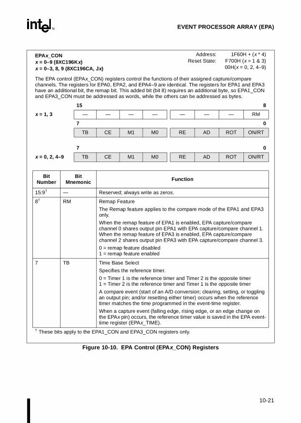
10-21
EVENT PROCESSOR ARRAY (EPA)
EPAx_CON x = 0–9 (8XC196Kx)x = 0–3, 8, 9 (8XC196CA, Jx)
Address:Reset State:
1F60H + (x * 4)F700H (x = 1 & 3)00H(x = 0, 2, 4–9)
The EPA control (EPAx_CON) registers control the functions of their assigned capture/compare channels. The registers for EPA0, EPA2, and EPA4–9 are identical. The registers for EPA1 and EPA3 have an additional bit, the remap bit. This added bit (bit 8) requires an additional byte, so EPA1_CON and EPA3_CON must be addressed as words, while the others can be addressed as bytes.
15 8
x = 1, 3 — — — — — — — RM
7 0
TB CE M1 M0 RE AD ROT ON/RT
7 0
x = 0, 2, 4–9 TB CE M1 M0 RE AD ROT ON/RT
BitNumber
Bit Mnemonic Function
15:9† — Reserved; always write as zeros.
8† RM Remap Feature
The Remap feature applies to the compare mode of the EPA1 and EPA3 only.
When the remap feature of EPA1 is enabled, EPA capture/compare channel 0 shares output pin EPA1 with EPA capture/compare channel 1. When the remap feature of EPA3 is enabled, EPA capture/compare channel 2 shares output pin EPA3 with EPA capture/compare channel 3.
0 = remap feature disabled1 = remap feature enabled
7 TB Time Base Select
Specifies the reference timer.
0 = Timer 1 is the reference timer and Timer 2 is the opposite timer1 = Timer 2 is the reference timer and Timer 1 is the opposite timer
A compare event (start of an A/D conversion; clearing, setting, or toggling an output pin; and/or resetting either timer) occurs when the reference timer matches the time programmed in the event-time register.
When a capture event (falling edge, rising edge, or an edge change on the EPAx pin) occurs, the reference timer value is saved in the EPA event-time register (EPAx_TIME).
† These bits apply to the EPA1_CON and EPA3_CON registers only.
Figure 10-10. EPA Control (EPA x_CON) Registers

8XC196Kx, Jx, CA USER’S MANUAL
10-22
6 CE Compare Enable
Determines whether the EPA channel operates in capture or compare mode.
0 = capture mode1 = compare mode
5:4 M1:0 EPA Mode Select
In capture mode, specifies the type of event that triggers an input capture. In compare mode, specifies the action that the EPA executes when the reference timer matches the event time.
M1 M0 Capture Mode Event
0 0 no capture0 1 capture on falling edge1 0 capture on rising edge1 1 capture on either edge
M1 M0 Compare Mode Action
0 0 no output0 1 clear output pin1 0 set output pin1 1 toggle output pin
3 RE Re-enable
Re-enable applies to the compare mode only. It allows a compare event to continue to execute each time the event-time register (EPAx_TIME) matches the reference timer rather than only upon the first time match.
0 = compare function is disabled after a single event1 = compare function always enabled
EPAx_CON (Continued)x = 0–9 (8XC196Kx)x = 0–3, 8, 9 (8XC196CA, Jx)
Address:Reset State:
1F60H + (x * 4)F700H (x = 1 & 3)00H(x = 0, 2, 4–9)
The EPA control (EPAx_CON) registers control the functions of their assigned capture/compare channels. The registers for EPA0, EPA2, and EPA4–9 are identical. The registers for EPA1 and EPA3 have an additional bit, the remap bit. This added bit (bit 8) requires an additional byte, so EPA1_CON and EPA3_CON must be addressed as words, while the others can be addressed as bytes.
15 8
x = 1, 3 — — — — — — — RM
7 0
TB CE M1 M0 RE AD ROT ON/RT
7 0
x = 0, 2, 4–9 TB CE M1 M0 RE AD ROT ON/RT
BitNumber
Bit Mnemonic Function
† These bits apply to the EPA1_CON and EPA3_CON registers only.
Figure 10-10. EPA Control (EPA x_CON) Registers (Continued)
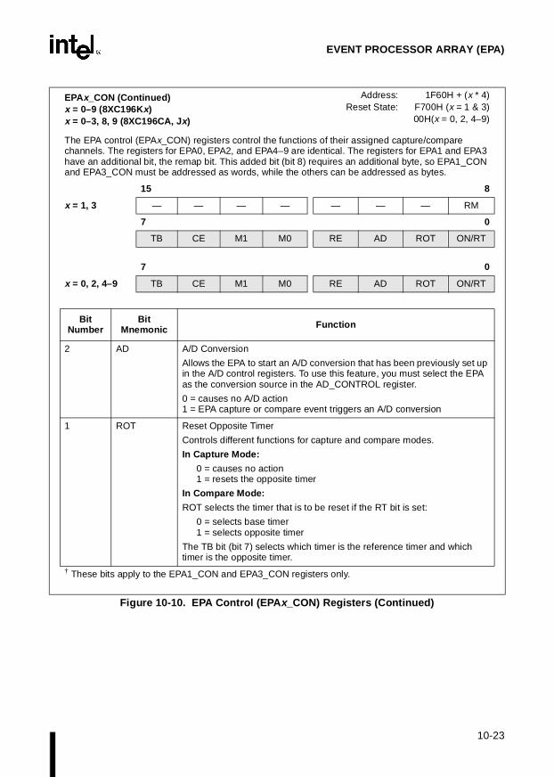
10-23
EVENT PROCESSOR ARRAY (EPA)
2 AD A/D Conversion
Allows the EPA to start an A/D conversion that has been previously set up in the A/D control registers. To use this feature, you must select the EPA as the conversion source in the AD_CONTROL register.
0 = causes no A/D action1 = EPA capture or compare event triggers an A/D conversion
1 ROT Reset Opposite Timer
Controls different functions for capture and compare modes.
In Capture Mode:
0 = causes no action1 = resets the opposite timer
In Compare Mode:
ROT selects the timer that is to be reset if the RT bit is set:
0 = selects base timer1 = selects opposite timer
The TB bit (bit 7) selects which timer is the reference timer and which timer is the opposite timer.
EPAx_CON (Continued)x = 0–9 (8XC196Kx)x = 0–3, 8, 9 (8XC196CA, Jx)
Address:Reset State:
1F60H + (x * 4)F700H (x = 1 & 3)00H(x = 0, 2, 4–9)
The EPA control (EPAx_CON) registers control the functions of their assigned capture/compare channels. The registers for EPA0, EPA2, and EPA4–9 are identical. The registers for EPA1 and EPA3 have an additional bit, the remap bit. This added bit (bit 8) requires an additional byte, so EPA1_CON and EPA3_CON must be addressed as words, while the others can be addressed as bytes.
15 8
x = 1, 3 — — — — — — — RM
7 0
TB CE M1 M0 RE AD ROT ON/RT
7 0
x = 0, 2, 4–9 TB CE M1 M0 RE AD ROT ON/RT
BitNumber
Bit Mnemonic Function
† These bits apply to the EPA1_CON and EPA3_CON registers only.
Figure 10-10. EPA Control (EPA x_CON) Registers (Continued)
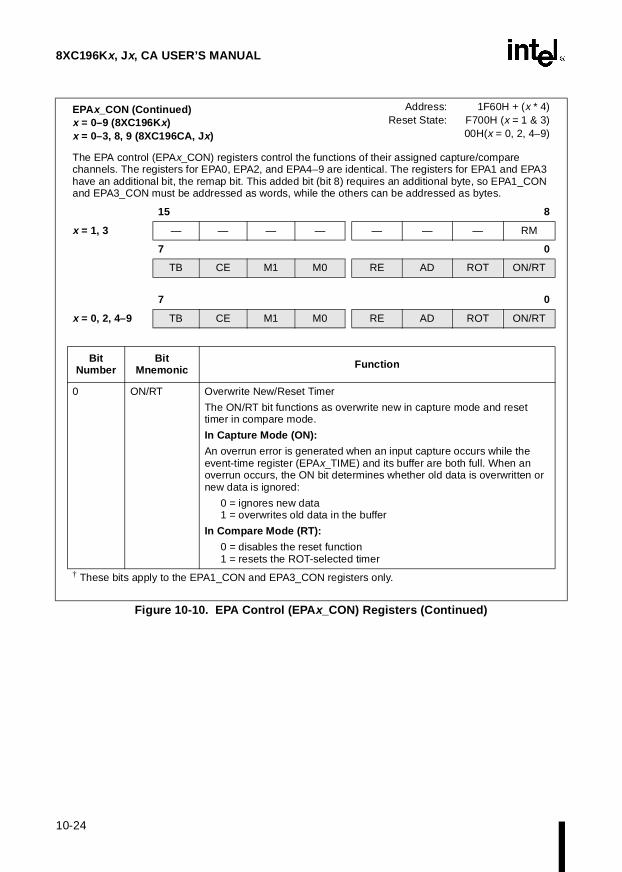
8XC196Kx, Jx, CA USER’S MANUAL
10-24
0 ON/RT Overwrite New/Reset Timer
The ON/RT bit functions as overwrite new in capture mode and reset timer in compare mode.
In Capture Mode (ON):
An overrun error is generated when an input capture occurs while the event-time register (EPAx_TIME) and its buffer are both full. When an overrun occurs, the ON bit determines whether old data is overwritten or new data is ignored:
0 = ignores new data1 = overwrites old data in the buffer
In Compare Mode (RT):
0 = disables the reset function1 = resets the ROT-selected timer
EPAx_CON (Continued)x = 0–9 (8XC196Kx)x = 0–3, 8, 9 (8XC196CA, Jx)
Address:Reset State:
1F60H + (x * 4)F700H (x = 1 & 3)00H(x = 0, 2, 4–9)
The EPA control (EPAx_CON) registers control the functions of their assigned capture/compare channels. The registers for EPA0, EPA2, and EPA4–9 are identical. The registers for EPA1 and EPA3 have an additional bit, the remap bit. This added bit (bit 8) requires an additional byte, so EPA1_CON and EPA3_CON must be addressed as words, while the others can be addressed as bytes.
15 8
x = 1, 3 — — — — — — — RM
7 0
TB CE M1 M0 RE AD ROT ON/RT
7 0
x = 0, 2, 4–9 TB CE M1 M0 RE AD ROT ON/RT
BitNumber
Bit Mnemonic Function
† These bits apply to the EPA1_CON and EPA3_CON registers only.
Figure 10-10. EPA Control (EPA x_CON) Registers (Continued)

10-25
EVENT PROCESSOR ARRAY (EPA)
10.5.4 Programming the Compare-only Channels
To program a compare event, you must first write to the COMPx_CON (Figure 10-11) register toconfigure the compare-only channel and then load the event time into COMPx_TIME.COMPx_CON has the same bits and settings as EPAx_CON. COMPx_TIME is functionally iden-tical to EPAx_TIME.
COMPx_CON x = 0–1
Address:
Reset State:
x = 0, 1F88Hx = 1, 1F8CH
00H
The EPA compare control (COMPx_CON) registers determine the function of the EPA compare channels.
7 0
TB CE M1 M0 RE AD ROT RT
Bit Number
Bit Mnemonic Function
7 TB Time Base Select
Specifies the reference timer.
1 = timer 2 is the reference timer and timer 1 is the opposite timer0 = timer 1 is the reference timer and timer 2 is the opposite timer
A compare event (start of an A/D conversion; clearing, setting, or toggling an output pin; and/or resetting either timer) occurs when the reference timer matches the time programmed in the event-time register.
6 CE Compare Enable
This bit enables the compare function.
1 = compare function enabled0 = compare function disabled
5:4 M1:0 EPA Mode Select
Specifies the type of compare event.
M1 M0
0 0 no output0 1 clear output pin1 0 set output pin1 1 toggle output pin
3 RE Re-enable
Allows a compare event to continue to execute each time the event-time register (COMPx_TIME) matches the reference timer rather than only upon the first time match.
1 = compare function always enabled0 = compare function will drive the output only once.
Figure 10-11. EPA Compare Control (COMP x_CON) Registers

8XC196Kx, Jx, CA USER’S MANUAL
10-26
10.6 ENABLING THE EPA INTERRUPTS
The EPA generates four individual event interrupts, EPA0–EPA3, and the multiplexed event in-terrupt, EPAx. To enable the interrupts, set the corresponding bits in the INT_MASK register(Figure 5-5 on page 5-13). To enable the individual sources of the multiplexed EPAx interrupt,set the corresponding bits in the EPA_MASK (Figure 10-12) and EPA_MASK1(Figure 10-13)registers. (Chapter 5, “Standard and PTS Interrupts,” discusses the interrupts in greater detail.)
2 AD A/D Conversion
Allows the EPA to start an A/D conversion that has been previously set up in the A/D control registers. To use this feature, you must select the EPA as the conversion source in the AD_CONTROL register.
1 = EPA compare event triggers an A/D conversion0 = causes no A/D action
1 ROT Reset Opposite Timer and Reset Timer
These bits control whether an EPA compare event resets the reference timer or the opposite timer.
ROT RTX 0 reset function disabled0 1 resets reference timer1 1 resets opposite timer
The state of the TB bit (COMPx_CON.7) determines which timer is the reference timer and which timer is the opposite timer.
0 RT Reset Timer
This bit controls whether the timer selected by the ROT bit will be reset
1 = resets the timer selected by the ROT bit0 = disables the reset function
COMPx_CON (Continued)x = 0–1
Address:
Reset State:
x = 0, 1F88Hx = 1, 1F8CH
00H
The EPA compare control (COMPx_CON) registers determine the function of the EPA compare channels.
7 0
TB CE M1 M0 RE AD ROT RT
Bit Number
Bit Mnemonic Function
Figure 10-11. EPA Compare Cont rol (COMP x_CON) Registers (Continued)

10-27
EVENT PROCESSOR ARRAY (EPA)
EPA_MASK Address:Reset State:
1FA0H0000H
The EPA interrupt mask (EPA_MASK) register enables or disables (masks) interrupts associated with the multiplexed EPAx interrupt.
15 8
CA, Jx — — — — EPA8 EPA9 OVR0 OVR1
7 0
0VR2 OVR3 — — — — OVR8 OVR9
15 8
Kx EPA4 EPA5 EPA6 EPA7 EPA8 EPA9 OVR0 OVR1
7 0
OVR2 OVR3 OVR4 OVR5 OVR6 OVR7 OVR8 OVR9
BitNumber Function
15:0† Setting a bit enables the corresponding interrupt as a multiplexed EPAx interrupt source. The multiplexed EPAx interrupt is enabled by setting its interrupt enable bit in the interrupt mask register (INT_MASK.0 = 1).
† Bits 2–5 and 12–15 are reserved on the 8XC196CA, Jx devices. For compatibility with future devices, write zeros to these bits.
Figure 10-12. EPA Interrupt Mask (EPA_MASK) Register
EPA_MASK1 Address:Reset State:
1FA4H00H
The EPA interrupt mask 1 (EPA_MASK1) register enables or disables (masks) interrupts associated with the EPAx interrupt.
7 0
— — — — COMP0 COMP1 OVRTM1 OVRTM2
Bit Number Function
7:4 Reserved; for compatibility with future devices, write zeros to these bits.
3:0 Setting a bit enables the corresponding interrupt as a multiplexed EPAx interrupt source. The multiplexed EPAx interrupt is enabled by setting its interrupt enable bit in the interrupt mask register (INT_MASK.0 = 1).
Figure 10-13. EPA Interrupt Mask 1 (EPA_MASK1) Register
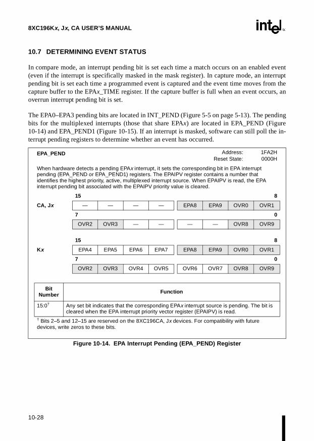
8XC196Kx, Jx, CA USER’S MANUAL
10-28
10.7 DETERMINING EVENT STATUS
In compare mode, an interrupt pending bit is set each time a match occurs on an enabled event(even if the interrupt is specifically masked in the mask register). In capture mode, an interruptpending bit is set each time a programmed event is captured and the event time moves from thecapture buffer to the EPAx_TIME register. If the capture buffer is full when an event occurs, anoverrun interrupt pending bit is set.
The EPA0–EPA3 pending bits are located in INT_PEND (Figure 5-5 on page 5-13). The pendingbits for the multiplexed interrupts (those that share EPAx) are located in EPA_PEND (Figure10-14) and EPA_PEND1 (Figure 10-15). If an interrupt is masked, software can still poll the in-terrupt pending registers to determine whether an event has occurred.
EPA_PEND Address:Reset State:
1FA2H0000H
When hardware detects a pending EPAx interrupt, it sets the corresponding bit in EPA interrupt pending (EPA_PEND or EPA_PEND1) registers. The EPAIPV register contains a number that identifies the highest priority, active, multiplexed interrupt source. When EPAIPV is read, the EPA interrupt pending bit associated with the EPAIPV priority value is cleared.
15 8
CA, Jx — — — — EPA8 EPA9 OVR0 OVR1
7 0
OVR2 OVR3 — — — — OVR8 OVR9
15 8
Kx EPA4 EPA5 EPA6 EPA7 EPA8 EPA9 OVR0 OVR1
7 0
OVR2 OVR3 OVR4 OVR5 OVR6 OVR7 OVR8 OVR9
BitNumber Function
15:0† Any set bit indicates that the corresponding EPAx interrupt source is pending. The bit is cleared when the EPA interrupt priority vector register (EPAIPV) is read.
† Bits 2–5 and 12–15 are reserved on the 8XC196CA, Jx devices. For compatibility with future devices, write zeros to these bits.
Figure 10-14. EPA Interrupt Pending (EPA_PEND) Register

10-29
EVENT PROCESSOR ARRAY (EPA)
10.8 SERVICING THE MULTIPLEXED EPA INTERRUPT WITH SOFTWARE
The multiplexed interrupts (those represented by EPAx) should be serviced with a standard inter-rupt service routine rather than the PTS (Chapter 5, “Standard and PTS Interrupts”). The PTS cantake only a limited number of actions, while interrupt service routines can be tailored to the needsof each interrupt.
The EPA_PEND (Figure 10-14) and EPA_PEND1 (Figure 10-15) registers contain the bits thatidentify the interrupt source(s). Traditionally, software would sort these bits to determine whichinterrupt service routine to execute. This sorting increases the overall interrupt response time bya significant number of states. However, the EPA interrupt priority vector register (EPAIPV, Fig-ure 10-16) contains a number that corresponds to the highest-priority active interrupt source (Ta-ble 10-7).
For example, assume that an overrun occurs on capture/compare channel 9 and no other multi-plexed interrupt is pending and unmasked. This sets the OVR9 pending bit in the EPA_PENDregister. If the corresponding mask bit is set in the EPA_MASK register, the EPAx interrupt pend-ing bit is set. If enabled, the EPAx interrupt is generated. The encoder places the number for theOVR9 interrupt (05H) into EPAIPV. Reading EPAIPV identifies capture/compare channel 9 asthe source, clears the OVR9 pending bit, and clears EPAIPV. When the device vectors to the EPAxinterrupt service routine, the EPAx pending bit is cleared. If other multiplexed interrupts have oc-curred, the encoder loads the number that corresponds to the highest-priority, active, multiplexedinterrupt into EPAIPV. When the EPAIPV register contains 00H, there are no more pending in-terrupts associated with the EPAx interrupt. Thus, it is recommended that the EPAIPV register beread until it equals 00H to ensure that all pending, enabled interrupts are serviced.
EPA_PEND1 Address:Reset State:
1FA6H00H
When hardware detects a pending EPAx interrupt, it sets the corresponding bit in EPA interrupt pending (EPA_PEND or EPA_PEND1) registers. The EPAIPV register contains a number that identifies the highest priority, active, multiplexed interrupt source. When EPAIPV is read, the EPA interrupt pending bit associated with the EPAIPV priority value is cleared.
7 0
— — — — COMP0 COMP1 OVRTM1 OVRTM2
Bit Number Function
7:4 Reserved; always write as zeros.
3:0 Any set bit indicates that the corresponding EPAx interrupt source is pending. The bit is cleared when the EPA interrupt priority vector register (EPAIPV) is read.
Figure 10-15. EPA Interrupt Pending 1 (EPA_PEND1) Registers
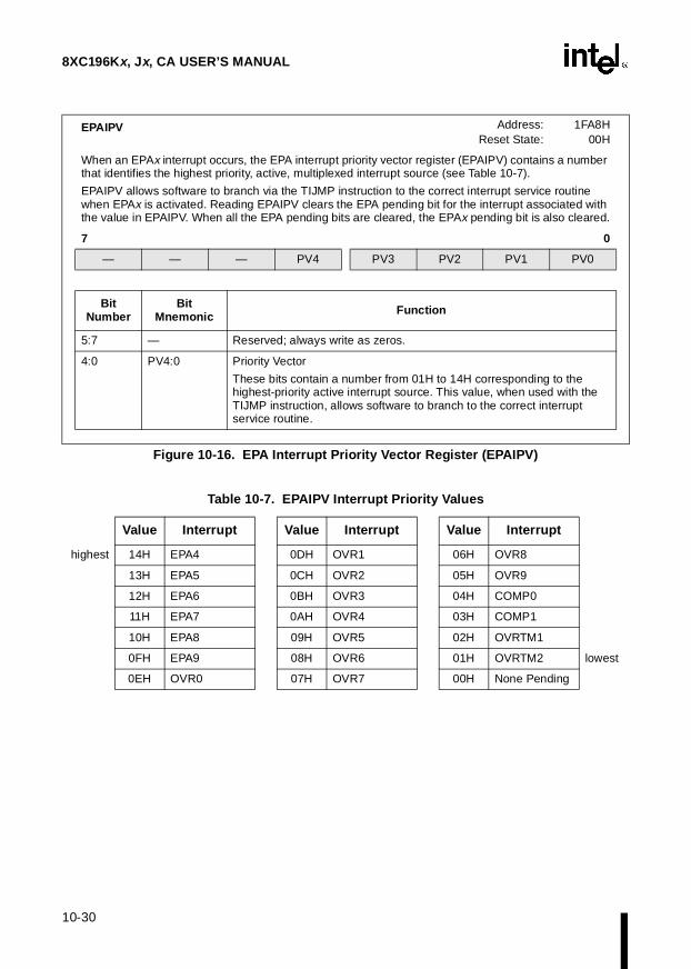
8XC196Kx, Jx, CA USER’S MANUAL
10-30
EPAIPV Address:Reset State:
1FA8H00H
When an EPAx interrupt occurs, the EPA interrupt priority vector register (EPAIPV) contains a number that identifies the highest priority, active, multiplexed interrupt source (see Table 10-7).
EPAIPV allows software to branch via the TIJMP instruction to the correct interrupt service routine when EPAx is activated. Reading EPAIPV clears the EPA pending bit for the interrupt associated with the value in EPAIPV. When all the EPA pending bits are cleared, the EPAx pending bit is also cleared.
7 0
— — — PV4 PV3 PV2 PV1 PV0
Bit Number
Bit Mnemonic Function
5:7 — Reserved; always write as zeros.
4:0 PV4:0 Priority Vector
These bits contain a number from 01H to 14H corresponding to the highest-priority active interrupt source. This value, when used with the TIJMP instruction, allows software to branch to the correct interrupt service routine.
Figure 10-16. EPA Interrupt Priority Vector Register (EPAIPV)
Table 10-7. EPAIPV Interrupt Priority Values
Value Interrupt Value Interrupt Value Interrupt
highest 14H EPA4 0DH OVR1 06H OVR8
13H EPA5 0CH OVR2 05H OVR9
12H EPA6 0BH OVR3 04H COMP0
11H EPA7 0AH OVR4 03H COMP1
10H EPA8 09H OVR5 02H OVRTM1
0FH EPA9 08H OVR6 01H OVRTM2 lowest
0EH OVR0 07H OVR7 00H None Pending

10-31
EVENT PROCESSOR ARRAY (EPA)
10.8.1 Using the TIJMP Instruction to Reduce Interrupt Service Overhead
The EPAIPV register and the TIJMP instruction can be used together to reduce the interrupt ser-vice overhead. The primary purpose of the TIJMP instruction is to reduce the interrupt responsetime associated with servicing multiplexed interrupts. With TIJMP, the additional time requiredto service interrupts is only the instruction time, 15 states. (See Appendix A for additional infor-mation about TIJMP.)
The format for the TIJMP instruction is TIJMP tbase,[index],#index_mask
where:
tbase is a word register containing the 16-bit starting address of the jumptable.
[index] is a word register containing a 16-bit address that points to a registerthat contains a 7-bit value used to calculate the offset into the jumptable.
#index_mask is 7-bit immediate data to mask the index. This value is ANDed withthe 7-bit value pointed to by [index] and multiplies the result by twoto determine the offset into the jump table.
TIJMP calculates the destination address as follows:
([index] AND #index_mask) × 2 + tbase
To use the TIJMP instruction in this application, you would create a jump table with 21 destina-tion addresses; one for each of the 20 EPA interrupt sources and one for the return.
The following code is a simplified example of an interrupt service routine that uses the EPAIPVregister with the TIJMP instruction to service an EPAx interrupt. This routine services all activeinterrupts in the EPA in order of their priority. The TIJMP instruction calculates an offset to fetcha word from a jump table (JTBASE in this example) which contains the start addresses of the in-terrupt service routines.

8XC196Kx, Jx, CA USER’S MANUAL
10-32
INIT_INTERRUPTS:LD JTBASE_PTR,#LSW JTBASE ;store jump table base address
EPAx_ISR:LD EPAIPV_PTR,#EPAIPV ;read EPAIPV offset
PUSHA ;save INT_MASK/INT_MASK1/WSR/PSWTIJMP JTBASE_PTR,[EPAIPV_PTR],#1FH ;initiate jump to correct ISR
OVR_EPA0_ISR: ;EPA0 overrun routine. ;. ;TIJMP JTBASE_PTR,[EPAIPV_PTR],#1FH
;check for pending ;interrupts, exit
EPAx_DONE:POPARET ;exit, all EPAx
;interrupts servicedJTBASE:
DCW LSW EPAx_done ;0 (no interrupt pending)DCW LSW OVR_TM2_ISR ;1 (Timer2 overflow)DCW LSW OVR_TM1_ISR ;2 (Timer1 overflow)DCW .DCW .DCW .DCW LSW OVR_EPA0_ISR ;0EH (EPA0 overflow)
This example assumes that EPAx is enabled, OVR0 is enabled, interrupts are globally enabled,and the capture/compare channel 0 has generated an OVR0 interrupt. This interrupt occurs whenan edge is detected on the EPA channel and both the input buffer and EPA0_TIME are full. Thiscauses software to enter the EPAx_ISR interrupt service routine.
Note that index_mask is set to 1FH . This sets the pointer to the end of the jump table to preventsoftware from jumping to an invalid address. Changing index_mask can dictate software control,thus superseding interrupt priorities.
Note that instead of a RET instruction at the end of OVR_EPA0_ISR, another TIJMP instructionis used. This is done to check for any other pending multiplexed interrupts. If EPAIPV containsa zero value (no pending interrupts) a vector to EPAx_DONE occurs and a RET is executed. Thisis to ensure that EPAIPV is cleared before the routine returns from the EPAx_ISR.

10-33
EVENT PROCESSOR ARRAY (EPA)
10.9 PROGRAMMING EXAMPLES FOR EPA CHANNELS
The three programming examples provided in this section demonstrate the use of the EPA channelfor a compare event, for a capture event, and for generation of a PWM signal. The programs dem-onstrate the detection of events by a polling scheme, by interrupts, and by the PTS. All three ex-amples were created using ApBUILDER, an interactive application program available throughIntel Literature Fulfillment or the Intel Applications Bulletin Board system (BBS). See Chapter1, “Guide to This Manual,” for information about ordering information from Intel Literature anddownloading files from the BBS. These sample program were written in the C programming lan-guage. ASM versions are also available from ApBUILDER.
NOTE
The initialization file (80c196kr.h) used in these examples is available from the Intel Applications BBS.
10.9.1 EPA Compare Event Program
This example C program demonstrates an EPA compare event. It sets up EPA channel 0 to toggleits output pin whenever timer 1 is zero. This program uses no interrupts; a polling scheme detectsthe EPA event. The program initializes EPA channel 0 for a compare event.
#pragma model(KR)#include <80c196kr.h>
#define COMPARE 0x40#define RE_ENABLE 0x08#define TOGGLE_PIN 0x30#define USE_TIMER1 0x00#define EPA0_INT_BIT 47
void init_epa0() epa0_con = COMPARE |
TOGGLE_PIN|RE_ENABLE |USE_TIMER1;
epa0_time = 0; setbit(p1_reg, 0); /* int reg */ clrbit(p1_dir, 0); /* make output pin */ setbit(p1_mode, 0);/* select EPA mode */
void init_timer1() t1control = COUNT_ENABLE |
COUNT_UP |CLOCK_INTERNAL |DIVIDE_BY_1;
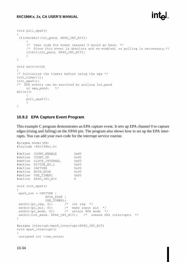
8XC196Kx, Jx, CA USER’S MANUAL
10-34
void poll_epa0() if(checkbit(int_pend, EPA0_INT_BIT))
/* User code for event channel 0 would go here. *//* Since this event is absolute and re-enabled, no polling is neccessary.*/
clrbit(int_pend, EPA0_INT_BIT);
void main(void)/* Initialize the timers before using the epa */init_timer1();init_epa0();/* EPA events can be serviced by polling int_pend or epa_pend. */while(1)
poll_epa0();
10.9.2 EPA Capture Event Program
This example C program demonstrates an EPA capture event. It sets up EPA channel 0 to captureedges (rising and falling) on the EPA0 pin. The program also shows how to set up the EPA inter-rupts. You can add your own code for the interrupt service routine.
#pragma model(KR)#include <80c196kr.h>
#define COUNT_ENABLE 0x80#define COUNT_UP 0x40#define CLOCK_INTERNAL 0x00#define DIVIDE_BY_1 0x00#define CAPTURE 0x00#define BOTH_EDGE 0x30#define USE_TIMER1 0x00#define EPA0_INT_BIT 4
void init_epa0() epa0_con = CAPTURE |
BOTH_EDGE |USE_TIMER1;
setbit(p1_reg, 0); /* int reg */ setbit(p1_dir, 0); /* make input pin */ setbit(p1_mode, 0); /* select EPA mode */ setbit(int_mask, EPA0_INT_BIT); /* unmask EPA interrupts */
#pragma interrupt(epa0_interrupt=EPA0_INT_BIT)void epa0_interrupt() unsigned int time_value;

10-35
EVENT PROCESSOR ARRAY (EPA)
time_value = epa0_time; /* must read to prevent overrun *//* To generate have code for the epax interrupt,select the ICU design screen.*/void init_timer1() t1control = COUNT_ENABLE |
COUNT_UP |CLOCK_INTERNAL |DIVIDE_BY_1;
void main(void) unsigned int time_value;
/* Initialize the timers and interrupts before using the EPA */ init_timer1(); init_epa0(); enable(); /* Globally enable interrupts */ while(1); /* loop forever, wait for interrupts to occur */
10.9.3 EPA PWM Output Program
This example C program demonstrates the generation of a PWM signal using the EPA’s PWMtoggle mode (see “PWM Modes” on page 5-31) and shows how to service the interrupts with thePTS. The PWM signal in this example has a 50% duty cycle.
#pragma model(KR)#include <80c196kr.h>#define PTS_BLOCK_BASE 0x98
/* Create typedef template for the PWM_TOGGLE mode control block.*/typedef struct PWM_toggle_ptscb_t
unsigned char unused;unsigned char ptscon;void *pts_ptr;unsigned int constant1;unsigned int constant2; PWM_toggle_ptscb;
/* This locates the PTS block mode control block in register ram. This *//* control block may be located at any quad-word boundary. */
register PWM_toggle_ptscb PWM_toggle_CB_3;#pragma locate(PWM_toggle_CB_3=PTS_BLOCK_BASE)
/* The PTS vector must contain the address of the PTS control block.*/#pragma pts(PWM_toggle_CB_3=0x3)

8XC196Kx, Jx, CA USER’S MANUAL
10-36
/* Sample PTS control block initialization sequence.*/
void Init_PWM_toggle_PTS3(void) disable(); /* disable all interrupts */ disable_pts(); /* disable the PTS interrupts */
PWM_toggle_CB_3.constant2 = 127; PWM_toggle_CB_3.constant1 = 127; PWM_toggle_CB_3.pts_ptr = (void *)&EPA0_TIME; PWM_toggle_CB_3.ptscon = 0x42;
/* Sample code that could be used to generate a PWM with an EPA channel.*/
setbit(p1_reg, 0x1); /* init output */ clrbit(p1_dir, 0x1); /* set to output */ setbit(p1_mode, 0x1); /* set special function*/ setbit(ptssel, 0x3); setbit(int_mask, 0x3)
void main(void) Init_PWM_toggle_PTS3(); epa1_con = 0x78; /* toggle, timer1, compare, re-enable */ epa1_timer = 127; t1control = 0xC2; /* enable timer, up 1 micrsecond @ 16 MHz */ enable_pts(); while(1);

11Analog-to-digital Converter


11-1
CHAPTER 11ANALOG-TO-DIGITAL CONVERTER
The analog-to-digital (A/D) converter can convert an analog input voltage to a digital value andset the A/D interrupt pending bit when it stores the result. It can also monitor a pin and set theA/D interrupt pending bit when the input voltage crosses over or under a programmed thresholdvoltage. This chapter describes the A/D converter and explains how to program it.
11.1 A/D CONVERTER FUNCTIONAL OVERVIEW
The A/D converter (Figure 11-1) can convert an analog input voltage to an 8- or 10-bit digitalresult and set the A/D interrupt pending bit when it stores the result. It can also monitor an inputand set the A/D interrupt pending bit when the input voltage crosses over or under the pro-grammed threshold voltage.
Figure 11-1. A/D Converter Block Diagram
Analog Mux
A2652-01
Succession Approximation
A/D Converter
Sample and Hold
VREF
EPA or PTS Command
Control Logic
AD_RESULT AD_COMMAND AD_TIME AD_TEST
ANGND
Status
* Multiplexed with port inputs
Analog Inputs *

8XC196Kx, Jx, CA USER’S MANUAL
11-2
11.2 A/D CONVERTER SIGNALS AND REGISTERS
Table 11-1 lists the A/D signals and Table 11-2 describes the control and status registers. Al-though the analog inputs are multiplexed with I/O port pins, no configuration is necessary.
Table 11-1. A/D Converter Pins
Port Pin A/D Signal A/D Signal Type Description
P0.7:0P0.7:2
ACH7:0 (Kx)ACH7:2 (CA, Jx)
I Analog Inputs
Input channels to the A/D converter. See the “Voltage on Analog Input Pin” specification in the datasheet for acceptable voltage ranges.
— ANGND GND Reference Ground
Must be connected for A/D converter and port operation.
— VREF PWR Reference Voltage
Must be connected for A/D converter and port operation.
Table 11-2. A/D Control and Status Registers
Mnemonic Address Description
AD_COMMAND 1FACH A/D Command
This register selects the A/D channel, controls whether the A/D conversion starts immediately or is triggered by the EPA, and selects the operating mode.
AD_RESULT 1FAAH, 1FABH A/D Result
For an A/D conversion, the high byte contains the eight MSBs from the conversion, while the low byte contains the two LSBs from a 10-bit conversion (undefined for an 8-bit conversion), indicates which A/D channel was used, and indicates whether the channel is idle.
For a threshold-detection, calculate the value for the successive approximation register and write that value to the high byte of AD_RESULT. Clear the low byte or leave it in its default state.
AD_TEST 1FAEH A/D Conversion Test
This register enables conversions on ANGND and VREF and specifies adjustments for zero-offset errors.
AD_TIME 1FAFH A/D Conversion Time
This register defines the sample window time and the conversion time for each bit.
INT_MASK 0008H Interrupt Mask
The AD bit in this register enables or disables the A/D interrupt. Set the AD bit to enable the interrupt request.
INT_PEND 0009H Interrupt Pending
The AD bit in this register, when set, indicates that an A/D interrupt request is pending.

11-3
ANALOG-TO-DIGITAL CONVERTER
11.3 A/D CONVERTER OPERATION
An A/D conversion converts an analog input voltage to a digital value, stores the result in theAD_RESULT register, and sets the A/D interrupt pending bit. An 8-bit conversion provides20 mV resolution, while a 10-bit conversion provides 5 mV resolution. An 8-bit conversion takesless time than a 10-bit conversion because it has two fewer bits to resolve and the comparator re-quires less settling time for 20 mV resolution than for 5 mV resolution.
You can convert the either the voltage on an analog input channel or a test voltage. Convertingthe test inputs allows you to calculate the zero-offset error, and the zero-offset adjustment allowsyou to compensate for it. This feature can reduce or eliminate off-chip compensation hardware.Typically, you would convert the test voltages and adjust for the zero-offset error before perform-ing conversions on an input channel. The AD_TEST register allows you to select a test voltageand program a zero-offset adjustment.
A threshold-detection compares an input voltage to a programmed reference voltage and sets theA/D interrupt pending bit when the input voltage crosses over or under the reference voltage.
A conversion can be started by a write to the AD_COMMAND register or it can be initiated bythe EPA, which can provide equally spaced samples or synchronization with external events.(See“Programming the EPA and Timer/Counters” on page 10-17.) The A/D scan mode of the pe-ripheral transaction server (PTS) allows you to perform multiple conversions and store their re-sults. (See “A/D Scan Mode” on page 5-26.)
Once the A/D converter receives the command to start a conversion, a delay time elapses beforesampling begins. (EPA-initiated conversions begin after the capture/compare event. Immediateconversions, those initiated directly by a write to AD_COMMAND, begin within three statetimes after the instruction is completed.) During this sample delay, the hardware clears the suc-cessive approximation register and selects the designated multiplexer channel. After the sampledelay, the device connects the multiplexer output to the sample capacitor for the specified sampletime. After this sample window closes, it disconnects the multiplexer output from the sample ca-pacitor so that changes on the input pin will not alter the stored charge while the conversion is inprogress. The device then zeros the comparator and begins the conversion.
P0_PIN 1FDAH Port 0 Pin State
Read P0_PIN to determine the current values of the port 0 pins. Reading the port induces noise into the A/D converter, decreasing the accuracy of any conversion in progress. We strongly recommend that you not read the port while an A/D conversion is in progress. To reduce noise, the P0_PIN register is clocked only when the port is read.
Table 11-2. A/D Control and Status Registers (Cont inued)
Mnemonic Address Description

8XC196Kx, Jx, CA USER’S MANUAL
11-4
The A/D converter uses a successive approximation algorithm to perform the analog-to-digitalconversion. The converter hardware consists of a 256-resistor ladder, a comparator, coupling ca-pacitors, and a 10-bit successive approximation register (SAR) with logic that guides the process.The resistive ladder provides 20 mV steps (VREF = 5.12 volts), while capacitive coupling creates5 mV steps within the 20 mV ladder voltages. Therefore, 1024 internal reference voltage levelsare available for comparison against the analog input to generate a 10-bit conversion result. In 8-bit conversion mode, only the resistive ladder is used, providing 256 internal reference voltagelevels.
The successive approximation conversion compares a sequence of reference voltages to the ana-log input, performing a binary search for the reference voltage that most closely matches the in-put. The ½ full scale reference voltage is the first tested. This corresponds to a 10-bit result wherethe most-significant bit is zero and all other bits are ones (0111111111B). If the analog input wasless than the test voltage, bit 10 of the SAR is left at zero, and a new test voltage of ¼ full scale(0011111111B) is tried. If the analog input was greater than the test voltage, bit 9 of SAR is set.Bit 8 is then cleared for the next test (0101111111B). This binary search continues until 10 (or 8)tests have occurred, at which time the valid conversion result resides in the AD_RESULT registerwhere it can be read by software. The result is equal to the ratio of the input voltage divided bythe analog supply voltage. If the ratio is 1.00, the result will be all ones.
11.4 PROGRAMMING THE A/D CONVERTER
The following A/D converter parameters are programmable:
• conversion input — input channel or test voltage (ANGND or VREF)
• zero-offset adjustment — no adjustment, plus 2.5 mV, minus 2.5 mV, or minus 5.0 mV
• conversion times — sample window time and conversion time for each bit
• operating mode — 8- or 10-bit conversion or 8-bit high or low threshold detection
• conversion trigger — immediate or EPA starts
This section describes the A/D converters’s registers and explains how to program them.

11-5
ANALOG-TO-DIGITAL CONVERTER
11.4.1 Programming the A/D Test Register
The AD_TEST register (Figure 11-2) selects either an analog input or a test voltage (ANGND orVREF) for conversion and specifies an offset voltage to be applied to the resistor ladder. To use thezero-offset adjustment, first perform two conversions, one on ANGND and one on VREF. With theresults of these conversions, use a software routine to calculate the zero-offset error. Specify thezero-offset adjustment by writing the appropriate value to AD_TEST. This offset voltage is addedto the resistor ladder and applies to all input channels. “Understanding A/D Conversion Errors”on page 11-14 describes zero-offset and other errors inherent in A/D conversions.
AD_TEST Address:Reset State:
1FAEHC0H
The A/D test (AD_TEST) register enables conversions on ANGND and VREF and specifies adjustments for DC offset errors. Its functions allow you to perform two conversions, one on ANGND and one on VREF. With these results, a software routine can calculate the offset and gain errors.
7 0
— — — — OFF1 OFF0 TV TE
Bit Number
Bit Mnemonic Function
7:4 — Reserved; for compatibility with future devices, write zeros to these bits.
3:2 OFF1:0 Offset
These bits allows you to set the zero-offset point.
OFF1 OFF0
0 0 no adjustment0 1 add 2.5 mV1 0 subtract 2.5 mV1 1 subtract 5.0 mV
1 TV Test Voltage
This bit selects the test voltage for a test mode conversion.
1 = VREF0 = ANGND
0 TE Test Enable
This bit determines whether normal or test mode conversions will be performed. A normal conversion converts the analog signal input on one of the analog input channels. A test conversion allows you to perform a conversion on ANGND or VREF.
1 = test0 = normal
Figure 11-2. A/D Test (AD_TEST) Register

8XC196Kx, Jx, CA USER’S MANUAL
11-6
11.4.2 Programming the A/D Result Register (for Threshold Detection Only)
To use the threshold-detection modes, you must first write a value to the high byte ofAD_RESULT to set the desired reference (threshold) voltage.
11.4.3 Programming the A/D Time Register
Two parameters, sample time and conversion time, control the time required for an A/D conver-sion. The sample time is the length of time that the analog input voltage is actually connected tothe sample capacitor. If this time is too short, the sample capacitor will not charge completely. Ifthe sample time is too long, the input voltage may change and cause conversion errors. The con-version time is the length of time required to convert the analog input voltage stored on the samplecapacitor to a digital value. The conversion time must be long enough for the comparator and cir-cuitry to settle and resolve the voltage. Excessively long conversion times allow the sample ca-pacitor to discharge, degrading accuracy.
AD_RESULT (Write) Address:Reset State:
1FAAH7F80H
The high byte of the A/D result (AD_RESULT) register can be written to set the reference voltage for the A/D threshold-detection modes.
15 8
REFV7 REFV6 REFV5 REFV4 REFV3 REFV2 REFV1 REFV0
7 0
— — — — — — — —
Bit Number
Bit Mnemonic Function
15:8 REFV7:0 Reference Voltage
These bits specify the threshold value. This selects a reference voltage that is compared with an analog input pin. When the voltage on the analog input pin crosses over (detect high) or under (detect low) the threshold value, the A/D interrupt flag is set.
Use the following formula to determine the value to write this register for a given threshold voltage.
7:0 — Reserved; for compatibility with future devices, write zeros to these bits.
Figure 11-3. A/D Result (AD_RESULT) Register — Write Format
reference voltagedesired threshold voltage 256×
VREF ANGND–-----------------------------------------------------------------------------------=

11-7
ANALOG-TO-DIGITAL CONVERTER
The AD_TIME register (Figure 11-4) specifies the A/D sample and conversion times. To avoiderroneous conversion results, use the TSAM and TCONV specifications on the datasheet to determineappropriate values.
AD_TIME Address:Reset State:
1FAFHFFH
The A/D time (AD_TIME) register programs the sample window time and the conversion time for each bit.
7 0
SAM2 SAM1 SAM0 CONV4 CONV3 CONV2 CONV1 CONV0
Bit Number
Bit Mnemonic Function
7:5 SAM2:0 A/D Sample Time
These bits specify the sample time. Use the following formula to compute the sample time.
where:SAM = 1 to 7TSAM = the sample time, in µsec, from the data sheetFOSC = the XTAL1 frequency, in MHz
4:0 CONV4:0 A/D Convert Time
These bits specify the conversion time for each bit. Use the following formula to compute the conversion time.
where:CONV= 2 to 31TCONV = the conversion time, in µsec, from the data sheetFOSC = the XTAL1 frequency, in MHzB = the number of bits to be converted (8 or 10)
NOTES:1. This register programs the speed at which the A/D can run — not the speed at which it can con-
vert correctly. Consult the data sheet for recommended values.2. Initialize the AD_TIME register before initializing the AD_COMMAND register.3. Do not write to this register while a conversion is in progress; the results are unpredictable.
Figure 11-4. A/D Time (AD_TIME) Register
SAMTSAM FOSC× 2–
8--------------------------------------------=
CONVTCONV FOSC× 3–
2 B×----------------------------------------------- 1–=
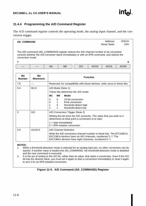
8XC196Kx, Jx, CA USER’S MANUAL
11-8
11.4.4 Programming the A/D Command Register
The A/D command register controls the operating mode, the analog input channel, and the con-version trigger.
AD_COMMAND Address:Reset State:
1FACHC0H
The A/D command (AD_COMMAND) register selects the A/D channel number to be converted, controls whether the A/D converter starts immediately or with an EPA command, and selects the conversion mode.
7 0
— — M1 M0 GO ACH2 ACH1 ACH0
Bit Number
Bit Mnemonic Function
7:6 — Reserved; for compatibility with future devices, write zeros to these bits.
5:4 M1:0 A/D Mode (Note 1)
These bits determine the A/D mode.
M1 M0 Mode
0 0 10-bit conversion0 1 8-bit conversion1 0 threshold detect high1 1 threshold detect low
3 GO A/D Conversion Trigger (Note 2)
Writing this bit arms the A/D converter. The value that you write to it determines at what point a conversion is to start.
1 = start immediately0 = EPA initiates conversion
2:0 ACH2:0 A/D Channel Selection
Write the A/D conversion channel number to these bits. The 87C196CA, 8XC196Jx devices have six A/D channels, numbered 2–7. The 8XC196Kx devices have eight channels, numbered 0–7.
NOTES:1. While a threshold-detection mode is selected for an analog input pin, no other conversion can be
started. If another value is loaded into AD_COMMAND, the threshold-detection mode is disabledand the new command is executed.
2. It is the act of writing to the GO bit, rather than its value, that starts a conversion. Even if the GObit has the desired value, you must set it again to start a conversion immediately or clear it againto arm it for an EPA-initiated conversion.
Figure 11-5. A/D Command (AD_COMMAND) Register

11-9
ANALOG-TO-DIGITAL CONVERTER
11.4.5 Enabling the A/D Interrupt
The A/D converter can set the A/D interrupt pending bit when it completes a conversion or whenthe input voltage crosses the threshold value in the selected direction. To enable the interrupt, setthe corresponding mask bit in the interrupt mask register (see Table 11-2 on page 11-2) and exe-cute the EI instruction to globally enable servicing of interrupts. The A/D interrupt can cause thePTS to begin a new conversion. See Chapter 5, “Standard and PTS Interrupts,” for details aboutinterrupts and a description of using the PTS in A/D scan mode.
11.5 DETERMINING A/D STATUS AND CONVERSION RESULTS
You can read the AD_RESULT register (Figure 11-6) to determine the status of the A/D convert-er. The AD_RESULT register is cleared when a new conversion is started; therefore, to preventlosing data, you must read both bytes before a new conversion starts. If you read AD_RESULTbefore the conversion is complete, the result is not guaranteed to be accurate.
The conversion result is the ratio of the input voltage to the reference voltage:
You can also read the interrupt pending register (see Table 11-2 on page 11-2) to determine thestatus of the A/D interrupt.
RESULT (8-bit) 255VIN ANGND–
VREF ANGND–-------------------------------------------×= RESULT (10-bit) 1023
VIN ANGND–
VREF ANGND–-------------------------------------------×=
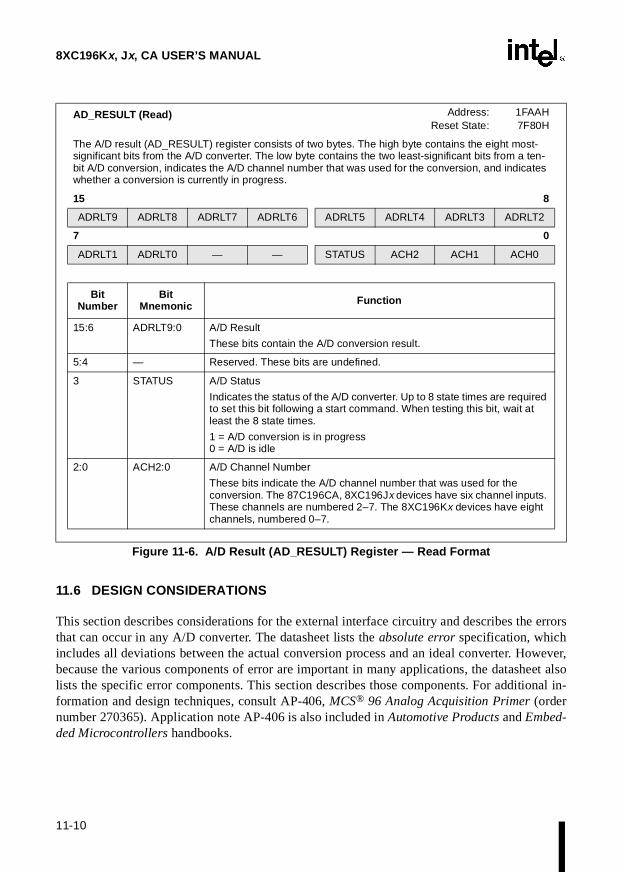
8XC196Kx, Jx, CA USER’S MANUAL
11-10
11.6 DESIGN CONSIDERATIONS
This section describes considerations for the external interface circuitry and describes the errorsthat can occur in any A/D converter. The datasheet lists the absolute error specification, whichincludes all deviations between the actual conversion process and an ideal converter. However,because the various components of error are important in many applications, the datasheet alsolists the specific error components. This section describes those components. For additional in-formation and design techniques, consult AP-406, MCS® 96 Analog Acquisition Primer (ordernumber 270365). Application note AP-406 is also included in Automotive Products and Embed-ded Microcontrollers handbooks.
AD_RESULT (Read) Address:Reset State:
1FAAH7F80H
The A/D result (AD_RESULT) register consists of two bytes. The high byte contains the eight most-significant bits from the A/D converter. The low byte contains the two least-significant bits from a ten-bit A/D conversion, indicates the A/D channel number that was used for the conversion, and indicates whether a conversion is currently in progress.
15 8
ADRLT9 ADRLT8 ADRLT7 ADRLT6 ADRLT5 ADRLT4 ADRLT3 ADRLT2
7 0
ADRLT1 ADRLT0 — — STATUS ACH2 ACH1 ACH0
Bit Number
Bit Mnemonic Function
15:6 ADRLT9:0 A/D Result
These bits contain the A/D conversion result.
5:4 — Reserved. These bits are undefined.
3 STATUS A/D Status
Indicates the status of the A/D converter. Up to 8 state times are required to set this bit following a start command. When testing this bit, wait at least the 8 state times.
1 = A/D conversion is in progress0 = A/D is idle
2:0 ACH2:0 A/D Channel Number
These bits indicate the A/D channel number that was used for the conversion. The 87C196CA, 8XC196Jx devices have six channel inputs. These channels are numbered 2–7. The 8XC196Kx devices have eight channels, numbered 0–7.
Figure 11-6. A/D Result (AD_ RESULT) Register — Read Format
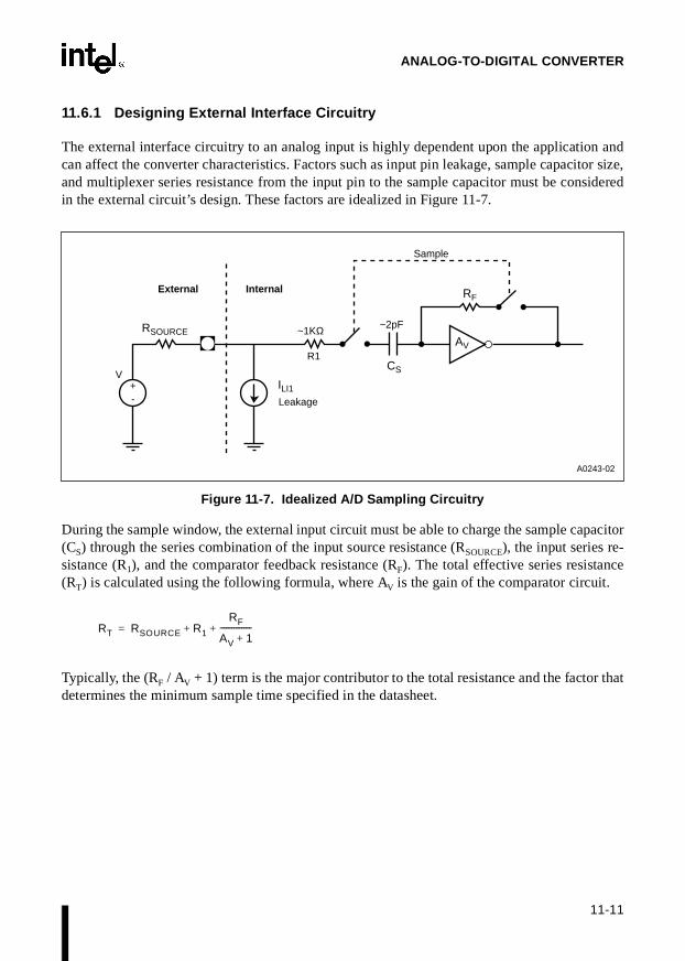
11-11
ANALOG-TO-DIGITAL CONVERTER
11.6.1 Designing External Interface Circuitry
The external interface circuitry to an analog input is highly dependent upon the application andcan affect the converter characteristics. Factors such as input pin leakage, sample capacitor size,and multiplexer series resistance from the input pin to the sample capacitor must be consideredin the external circuit’s design. These factors are idealized in Figure 11-7.
Figure 11-7. Idealized A/D Sampling Circuitry
During the sample window, the external input circuit must be able to charge the sample capacitor(CS) through the series combination of the input source resistance (RSOURCE), the input series re-sistance (R1), and the comparator feedback resistance (RF). The total effective series resistance(RT) is calculated using the following formula, where AV is the gain of the comparator circuit.
Typically, the (RF / AV + 1) term is the major contributor to the total resistance and the factor thatdetermines the minimum sample time specified in the datasheet.
Leakage
V
RSOURCE
+ -
CS
R1
~1KΩ ~2pF
ILI1
External Internal
AV
RF
Sample
A0243-02
RT RSOURCE R1
RF
AV 1+----------------+ +=

8XC196Kx, Jx, CA USER’S MANUAL
11-12
11.6.1.1 Minimizing the Effect of High Input Source Resistance
Under some conditions, the input source resistance (RSOURCE) can be great enough to affect themeasurement. You can minimize this effect by increasing the sample time or by connecting anexternal capacitor (CEXT) from the input pin to ANGND. The external signal will charge CEXT tothe source voltage level. When the channel is sampled, CEXT acts as a low-impedance source tocharge the sample capacitor (CS). A small portion of the charge in CEXT is transferred to CS, re-sulting in a drop of the sampled voltage. The voltage drop is calculated using the following for-mula.
If CEXT is 0.005 µF or greater, the error will be less than –0.4 LSB in 10-bit conversion mode. Theuse of CEXT in conjunction with RSOURCE forms a low-pass filter that reduces noise input to theA/D converter.
High RSOURCE resistance can also cause errors due to the input leakage (ILI1). ILI1 is typically muchlower than its specified maximum (consult the datasheet for specifications). The combined effectof ILI1 leakage and high RSOURCE resistance is calculated using the following formula.
where:
RSOURCE is the input source resistance, in ohms
ILI1 is the input leakage, in amperes
VREF is the reference voltage, in volts
External circuits with RSOURCE resistance of 1 KΩ or lower and VREF equal to 5.0 volts will havea resultant error due to source impedance of 0.6 LSB or less.
Sampled Voltage Drop, %CS
CEXT CS+--------------------------- 100%×=
error (LSBs)RSOURCE ILI1× 1024×
VREF
------------------------------------------------------------=

11-13
ANALOG-TO-DIGITAL CONVERTER
11.6.1.2 Suggested A/D Input Circuit
The suggested A/D input circuit shown in Figure 11-8 provides limited protection against over-voltage conditions on the analog input. Should the input voltage be driven significantly belowANGND or above VREF, diode D2 or D1 will forward bias at about 0.8 volts. The device’s inputprotection begins to turn on at approximately 0.5 volts beyond ANGND or VREF. The 270Ω re-sistor limits the current input to the analog input pin to a safe value, less than 1 mA.
NOTE
Driving any analog input more than 0.5 volts beyond ANGND or VREF begins to activate the input protection devices. This drives current into the internal reference circuitry and substantially degrades the accuracy of A/D conversions on all channels.
Thoroughly analyze the applicability of the circuit shown in Figure 11-8 before using it in an actual application.
Figure 11-8. Suggested A/D Input Circuit
11.6.1.3 Analog Ground and Reference Voltages
Reference supply levels strongly influence the absolute accuracy of the conversion. For this rea-son, we recommend that you tie the ANGND pin to the VSS pin as close to the device as possible,using a minimum trace length. In a noisy environment, we highly recommend the use of a sepa-rate analog ground plane that connects to VSS at a single point as close to the device as possible.IREF may vary between 2 mA and 5 mA during a conversion. To minimize the effect of this fluc-tuation, mount a 1.0 µF ceramic or tantalum bypass capacitor between VREF and ANGND, asclose to the device as possible.
Analog Input Pin
ANGND
(Optional)
D1
D2
270Ω100Ω
0.005µF
ANGND
A0082-02
VREF
VREF
From Application
System

8XC196Kx, Jx, CA USER’S MANUAL
11-14
ANGND should be within about ± 50 mV of VSS. VREF should be well regulated and used onlyfor the A/D converter. The VREF supply can be between 4.5 and 5.5 V and must be able to sourceapproximately 5 mA (see the datasheet for actual specifications). VREF should be approximatelythe same voltage as VCC. VREF and VCC should power up at the same time, to avoid potential latch-up conditions on VREF. Large negative current spikes on the ANGND pin relative to VSS maycause the analog circuitry to latch up. This is an additional reason to follow careful groundingpractice.
The analog voltage reference (VREF) is the positive supply to which all A/D conversions are com-pared. It is also the supply to port 0 if the A/D converter is not being used. If high accuracy is notrequired, VREF can be tied to VCC. If accuracy is important, VREF must be very stable. One way toaccomplish this is through the use of a precision power supply or a separate voltage regulator(usually an IC). These devices must be referenced to ANGND, not to VSS, to ensure that VREF
tracks ANGND and not VSS.
11.6.1.4 Using Mixed Analog and Digital Inputs
Port 0 may be used for both analog and digital input signals at the same time. However, readingthe port may inject some noise into the analog circuitry. For this reason, make certain that an an-alog conversion is not in progress when the port is read. Refer to Chapter 6, “I/O Ports,” for in-formation about using the port as digital inputs.
11.6.2 Understanding A/D Conversion Errors
The conversion result is the ratio of the input voltage to the reference voltage.
This ratio produces a stair-stepped transfer function when the output code is plotted versus inputvoltage. The resulting digital codes can be taken as simple ratiometric information, or they pro-vide information about absolute voltages or relative voltage changes on the inputs.
The more demanding the application, the more important it is to fully understand the converter’soperation. For simple applications, knowing the absolute error of the converter is sufficient.However, closing a servo-loop with analog inputs requires a detailed understanding of an A/Dconverter’s operation and errors.
RESULT (8-bit) 255VIN ANGND–
VREF ANGND–-------------------------------------------×= RESULT (10-bit) 1023
VIN ANGND–
VREF ANGND–-------------------------------------------×=

11-15
ANALOG-TO-DIGITAL CONVERTER
In many applications, it is less critical to record the absolute accuracy of an input than it is to de-tect that a change has occurred. This approach is acceptable as long as the converter is monotonicand has no missing codes. That is, increasing input voltages produce adjacent, unique outputcodes that are also increasing. Decreasing input voltages produce adjacent, unique output codesthat are also decreasing. In other words, there exists a unique input voltage range for each 10-bitoutput code that produces that code only, with a repeatability of typically ± 0.25 LSBs (1.5 mV).
The inherent errors in an analog-to-digital conversion process are quantizing error, zero-offset er-ror, full-scale error, differential nonlinearity, and nonlinearity. All of these are transfer functionerrors related to the A/D converter. In addition, temperature coefficients, VCC rejection, sample-hold feedthrough, multiplexer off-isolation, channel-to-channel matching, and random noiseshould be considered. Fortunately, one absolute error specification (listed in datasheets) de-scribes the total of all deviations between the actual conversion process and an ideal converter.However, the various components of error are important in many applications.
An unavoidable error results from the conversion of a continuous voltage to an integer digital rep-resentation. This error is called quantizing error and is always ± 0.5 LSB. Quantizing error is theonly error seen in a perfect A/D converter, and is obviously present in actual converters. Figure11-9 shows the transfer function for an ideal 3-bit A/D converter.

8XC196Kx, Jx, CA USER’S MANUAL
11-16
Figure 11-9. Ideal A/D Conversion Characteristic
Note that the ideal characteristic possesses unique qualities:
• its first code transition occurs when the input voltage is 0.5 LSB;
• its full-scale code transition occurs when the input voltage equals the full-scale referencevoltage minus 1.5 LSB (VREF – 1.5LSB); and
• its code widths are all exactly one LSB.
These qualities result in a digitization without zero-offset, full-scale, or linearity errors; in otherwords, a perfect conversion.
FINAL CODE TRANSITION OCCURS WHEN THE APPLIED VOLTAGE IS
EQUAL TO (Vref – 1.5 (LSB)).
ACTUAL CHARACTERISTIC OF AN IDEAL A/D CONVERTER
FIRST CODE TRANSITION OCCURS WHEN THE APPLIED VOLTAGE IS
EQUAL TO 1/2 LSB.
THE VOLTAGE CHANGE BETWEEN THE ADJACENT CODE
TRANSITIONS (THE “CODE WIDTH”) IS = 1 LSB.
1/2 1 2 3 4 5 6 7 86 1/2
0
1
2
3
4
5
6
7
INPUT VOLTAGE (LSBs)
Ø O
UT
PU
T C
OD
E, Q
A0083-01

11-17
ANALOG-TO-DIGITAL CONVERTER
Figure 11-10. Actual and Ideal A/D Conversion Char acteristics
The actual characteristic of a hypothetical 3-bit converter is not perfect. When the ideal charac-teristic is overlaid with the actual characteristic, the actual converter is seen to exhibit errors inthe locations of the first and final code transitions and in code widths, as shown in Figure 11-10.The deviation of the first code transition from ideal is called zero-offset error, and the deviationof the final code transition from ideal is full-scale error. The deviation of a code width from idealcauses two types of errors: differential nonlinearity and nonlinearity. Differential nonlinearity isa measure of local code-width error, whereas nonlinearity is a measure of overall code-transitionerror.
FULL SCALE ERROR
ZERO OFFSET
ACTUAL CHARACTERISTIC
1/2 1 2 3 4 5 6 7 86 1/2
0
1
2
3
4
5
6
7
INPUT VOLTAGE (LSBs)
Ø O
UT
PU
T C
OD
E, Q
ABSOLUTE ERROR
IDEAL CHARACTERISTIC
A0084-01

8XC196Kx, Jx, CA USER’S MANUAL
11-18
Differential nonlinearity is the degree to which actual code widths differ from the ideal one-LSBwidth. It provides a measure of how much the input voltage may have changed in order to producea one-count change in the conversion result. In the 10-bit converter, the code widths are ideally5 mV (VREF / 1024). If such a converter is specified to have a maximum differential nonlinearityof 2 LSBs (10 mV), then the maximum code width will be no greater than 10 mV larger than ide-al, or 15 mV.
Because the A/D converter has no missing codes, the minimum code width will always be greaterthan –1 (negative one). The differential nonlinearity error on a particular code width is compen-sated for by other code widths in the transfer function, such that 1024 unique steps occur. Theactual code widths in this converter typically vary from 2.5 mV to 7.5 mV.
Nonlinearity is the worst-case deviation of code transitions from the corresponding code transi-tions of the ideal characteristic. Nonlinearity describes the extent to which differential nonlinear-ities can add up to produce an overall maximum departure from a linear characteristic. If thedifferential nonlinearity errors are too large, it is possible for an A/D converter to miss codes orto exhibit non-monotonic behavior. Neither behavior is desirable in a closed-loop system. A con-verter has no missing codes if there exists for each output code a unique input voltage range thatproduces that code only. A converter is monotonic if every subsequent code change represents aninput voltage change in the same direction.
Differential nonlinearity and nonlinearity are quantified by measuring the terminal-based linear-ity errors. A terminal-based characteristic results when an actual characteristic is translated andscaled to eliminate zero-offset and full-scale error, as shown in Figure 11-11. The terminal-basedcharacteristic is similar to the actual characteristic that would result if zero-offset and full-scaleerror were externally trimmed away. In practice, this is done by using input circuits that includegain and offset trimming. In addition, VREF could also be closely regulated and trimmed withinthe specified range to affect full-scale error.
Other factors that affect a real A/D converter system include temperature drift, failure to com-pletely reject unwanted signals, multiplexer channel dissimilarities, and random noise. Fortunate-ly, these effects are small. Temperature drift is the rate at which typical specifications change witha change in temperature. These changes are reflected in the temperature coefficients. Unwantedsignals come from three main sources: noise on VCC, input signal changes on the channel beingconverted (after the sample window has closed), and signals applied to channels not selected bythe multiplexer. The effects of these unwanted signals are specified as Vcc rejection, off-isolation,and feedthrough, respectively. Finally, multiplexer on-channel resistances differ slightly from onechannel to the next, which causes channel-to-channel matching errors and repeatability errors.Differences in DC leakage current from one channel to another and random noise in general con-tribute to repeatability errors.
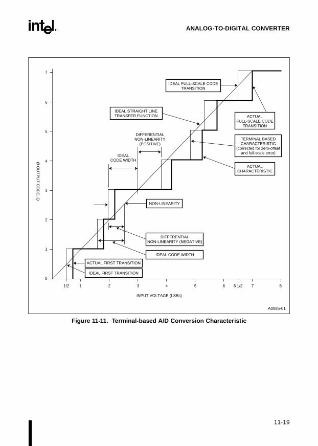
11-19
ANALOG-TO-DIGITAL CONVERTER
Figure 11-11. Terminal-based A/D Conversion Characteristic
IDEAL FULL-SCALE CODE TRANSITION
ACTUAL FIRST TRANSITION
1/2 1 2 3 4 5 6 7 86 1/2
0
1
2
3
4
5
6
7
INPUT VOLTAGE (LSBs)
Ø O
UT
PU
T C
OD
E, Q
IDEAL STRAIGHT LINE TRANSFER FUNCTION
NON-LINEARITY
DIFFERENTIAL NON-LINEARITY
(POSITIVE)
IDEAL CODE WIDTH
IDEAL FIRST TRANSITION
IDEAL CODE WIDTH
DIFFERENTIAL NON-LINEARITY (NEGATIVE)
ACTUAL CHARACTERISTIC
TERMINAL BASED CHARACTERISTIC
(corrected for zero-offset and full-scale error)
ACTUAL FULL-SCALE CODE
TRANSITION
A0085-01


12CAN Serial Communications Controller

<PageNum>-22

12-1
CHAPTER 12CAN SERIAL COMMUNICATIONS CONTROLLER
The 87C196CA has a peripheral not found in the 8XC196Kx and 8XC196Jx controllers — theCAN (controller area network) peripheral. The CAN serial communications controller managescommunications between multiple network nodes. This integrated peripheral is similar to Intel’sstandalone 82527 CAN serial communications controller. It supports both the standard and theextended message frames specified by CAN 2.0 protocol parts A and B developed by RobertBosch, GmbH. This chapter describes the integrated CAN controller and explains how to config-ure it. Consult Appendix B, “Signal Descriptions,” for detailed descriptions of the signals dis-cussed in this chapter.
12.1 CAN FUNCTIONAL OVERVIEW
The integrated CAN controller transfers messages between network nodes according to the CANprotocol. The CAN protocol uses a multiple-master, contention-based bus configuration, whichis also called CSMA/CR (carrier sense, multiple access, with collision resolution). Each CANcontroller’s input and output pins are connected to a two-line CAN bus through which all com-munication takes place (Figure 12-1).
Figure 12-1. A System Using CAN Controllers
196Cx device
Engine
ABS
82527
82527
Transmission
Dashboard
196Cx device
196Cx device C
AN
Bus
A2588-02
Bus Driver
CPU
CPUTx0
Rx0
Tx0
Rx0
Bus Driver
TXCAN
RXCAN
TXCAN
RXCAN
TXCAN
RXCAN
Bus Driver CAN_H
CAN_L
Bus Driver
Bus Driver CAN_H
CAN_L
Security System
CAN_H
CAN_L
CAN_H
CAN_L
CAN_H
CAN_L
Bus
Bus

8XC196Kx, Jx, CA USER’S MANUAL
12-2
This bus configuration reduces point-to-point wiring requirements, making the CAN controllerwell suited to automotive and factory automation applications. In addition, it relieves the CPU ofmuch of the communications burden while providing a high level of data integrity through errormanagement logic.
The CAN controller (Figure 12-2) has one input pin, one output pin, control and status registers,and error detection and management logic.
Figure 12-2. CAN Controller Block Diagram
Bit Timing Registers
Control Register
Status Register
Interrupt Register
Message Objects 1-14
Message Object 15
Global Mask
Registers
Mask 15 Register
RAM
Error Management
Logic
RXCAN
TXCAN
2
A2590-02
Bus Driver
Bus Driver
CAN Bus

12-3
CAN SERIAL COMMUNICATIONS CONTROLLER
12.2 CAN CONTROLLER SIGNALS AND REGISTERS
Table 12-1 describes the CAN controller’s pins, and Table 12-2 describes the control and statusregisters.
Table 12-1. CAN Controller Signals
Signal Type Description
RXCAN I Receive
This signal carries messages from other nodes on the CAN bus to the CAN controller.
TXCAN O Transmit
This signal carries messages from the CAN controller to other nodes on the CAN bus.
Table 12-2. Cont rol and Status Registers
Register Mnemonic ††
Register Address †† Description
CAN_BTIME0† 1E3FH Bit Timing 0
Program this register to define the length of one time quantum and the maximum number of time quanta by which a bit time can be modified for resynchronization.
CAN_BTIME1† 1E4FH Bit Timing 1
Program this register to define the sample time and mode.
CAN_CON† 1E00H Control
Program this register to prevent transfers to and from the CAN bus, to enable and disable CAN interrupts, and to control write access to the bit timing registers.
CAN_EGMSK 1E08H, 1E09H,1E0AH, 1E0BH
Extended Global Mask
Program this register to mask (“don’t care”) specific message identifier bits for extended message objects.
CAN_INT 1E5FH CAN Interrupt Pending
This read-only register indicates the source of the highest-priority pending interrupt.
CAN_MSGxCFG 1Ey6H Message Object x Configuration
Program this register to specify a message object’s data length, transfer direction, and identifier type.
CAN_MSGxCON0 1Ey0H Message Object x Control 0
Program this register to enable or disable the message object’s successful transmission (TX) and reception (RX) interrupts. Read this register to determine whether a message object is ready to transmit and whether an interrupt is pending.
†The CCE bit in CAN_CON must be set to enable write access to the bit timing registers.††In register names, x = 1–15; in addresses, y = 1–F.
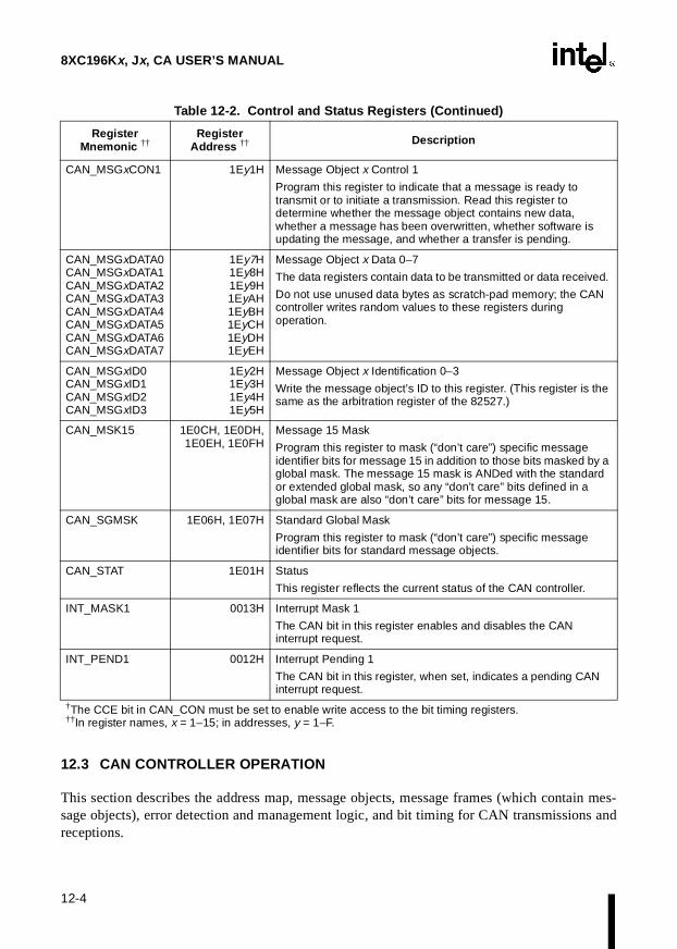
8XC196Kx, Jx, CA USER’S MANUAL
12-4
12.3 CAN CONTROLLER OPERATION
This section describes the address map, message objects, message frames (which contain mes-sage objects), error detection and management logic, and bit timing for CAN transmissions andreceptions.
CAN_MSGxCON1 1Ey1H Message Object x Control 1
Program this register to indicate that a message is ready to transmit or to initiate a transmission. Read this register to determine whether the message object contains new data, whether a message has been overwritten, whether software is updating the message, and whether a transfer is pending.
CAN_MSGxDATA0CAN_MSGxDATA1CAN_MSGxDATA2CAN_MSGxDATA3CAN_MSGxDATA4CAN_MSGxDATA5CAN_MSGxDATA6CAN_MSGxDATA7
1Ey7H1Ey8H1Ey9H1EyAH1EyBH1EyCH1EyDH1EyEH
Message Object x Data 0–7
The data registers contain data to be transmitted or data received.
Do not use unused data bytes as scratch-pad memory; the CAN controller writes random values to these registers during operation.
CAN_MSGxID0CAN_MSGxID1CAN_MSGxID2CAN_MSGxID3
1Ey2H1Ey3H1Ey4H1Ey5H
Message Object x Identification 0–3
Write the message object’s ID to this register. (This register is the same as the arbitration register of the 82527.)
CAN_MSK15 1E0CH, 1E0DH,1E0EH, 1E0FH
Message 15 Mask
Program this register to mask (“don’t care”) specific message identifier bits for message 15 in addition to those bits masked by a global mask. The message 15 mask is ANDed with the standard or extended global mask, so any “don’t care” bits defined in a global mask are also “don’t care” bits for message 15.
CAN_SGMSK 1E06H, 1E07H Standard Global Mask
Program this register to mask (“don’t care”) specific message identifier bits for standard message objects.
CAN_STAT 1E01H Status
This register reflects the current status of the CAN controller.
INT_MASK1 0013H Interrupt Mask 1
The CAN bit in this register enables and disables the CAN interrupt request.
INT_PEND1 0012H Interrupt Pending 1
The CAN bit in this register, when set, indicates a pending CAN interrupt request.
Table 12-2. Control and Status Registers (Continued)
Register Mnemonic ††
Register Address †† Description
†The CCE bit in CAN_CON must be set to enable write access to the bit timing registers.††In register names, x = 1–15; in addresses, y = 1–F.
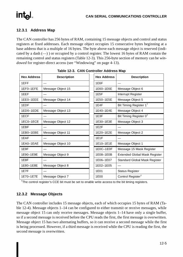
12-5
CAN SERIAL COMMUNICATIONS CONTROLLER
12.3.1 Address Map
The CAN controller has 256 bytes of RAM, containing 15 message objects and control and statusregisters at fixed addresses. Each message object occupies 15 consecutive bytes beginning at abase address that is a multiple of 16 bytes. The byte above each message object is reserved (indi-cated by a dash (—) ) or occupied by a control register. The lowest 16 bytes of RAM contain theremaining control and status registers (Table 12-3). This 256-byte section of memory can be win-dowed for register-direct access (see “Windowing” on page 4-13).
12.3.2 Message Objects
The CAN controller includes 15 message objects, each of which occupies 15 bytes of RAM (Ta-ble 12-4). Message objects 1–14 can be configured to either transmit or receive messages, whilemessage object 15 can only receive messages. Message objects 1–14 have only a single buffer,so if a second message is received before the CPU reads the first, the first message is overwritten.Message object 15 has two alternating buffers, so it can receive a second message while the firstis being processed. However, if a third message is received while the CPU is reading the first, thesecond message is overwritten.
Table 12-3. CAN Controller Address Map
Hex Address Description Hex Address Description
1EFF — 1E6F —
1EF0–1EFE Message Object 15 1E60–1E6E Message Object 6
1EEF — 1E5F Interrupt Register
1EE0–1EEE Message Object 14 1E50–1E5E Message Object 5
1EDF — 1E4F Bit Timing Register 1†
1ED0–1EDE Message Object 13 1E40–1E4E Message Object 4
1ECF — 1E3F Bit Timing Register 0†
1EC0–1ECE Message Object 12 1E30–1E3E Message Object 3
1EBF — 1E2F —
1EB0–1EBE Message Object 11 1E20–1E2E Message Object 2
1EAF — 1E1F —
1EA0–1EAE Message Object 10 1E10–1E1E Message Object 1
1E9F — 1E0C–1E0F Message 15 Mask Register
1E90–1E9E Message Object 9 1E08–1E0B Extended Global Mask Register
1E8F — 1E06–1E07 Standard Global Mask Register
1E80–1E8E Message Object 8 1E02–1E05 —
1E7F — 1E01 Status Register
1E70–1E7E Message Object 7 1E00 Control Register†
†The control register’s CCE bit must be set to enable write access to the bit timing registers.

8XC196Kx, Jx, CA USER’S MANUAL
12-6
12.3.2.1 Receive and Transmit Priorities
The lowest-numbered message object always has the highest priority, regardless of the messageidentifier. When multiple messages are ready to transmit, the CAN controller transmits the mes-sage from the lowest-numbered message object first. When multiple message objects are capableof receiving the same message, the lowest-numbered message object receives it. For example, ifall identifier bits are masked, message object 1 receives all messages.
12.3.2.2 Message Acceptance Fil tering
The mask registers provide a method for developing an acceptance filtering strategy for a specificsystem. Software can program the mask registers to require an exact match on specific identifierbits while masking (“don’t care”) the remaining bits. Without a masking strategy, a message ob-ject could accept only those messages with an identical message identifier. With a masking strat-egy in place, a message object can accept messages whose identifiers are not identical.
The CAN controller filters messages by comparing an incoming message’s identifier with that ofan enabled internal message object. The standard global mask register applies to messages withstandard (11-bit) identifiers, while the extended global mask register applies to those with extend-ed (29-bit) identifiers. The CAN controller applies the appropriate global mask to each incomingmessage identifier and checks for an acceptance match in message objects 1–14. If no match ex-ists, it then applies the message 15 mask and checks for a match on message object 15. The mes-sage 15 mask is ANDed with the global mask, so any bit that is masked by the global mask isautomatically masked for message 15.
The CAN controller accepts an incoming data message if the message’s identifier matches that ofany enabled receive message object. It accepts an incoming remote message (request for datatransmission) if the message’s identifier matches that of any enabled transmit message object.The remote message’s identifier is stored in the transmit message object, overwriting any maskedbits. Table 12-5 shows an example.
Table 12-4. Message Object Structure
Hex Address † Contents
1Ex7–1ExE Data Bytes 0–7
1Ex6 Message Configuration
1Ex2–1Ex5 Message Identifier 0–3
1Ex0–1Ex1 Message Control 0–1† x = message object number, in hexadecimal

12-7
CAN SERIAL COMMUNICATIONS CONTROLLER
12.3.3 Message Frames
A message object is contained within a message frame that adds control and error-detection bitsto the content of the message object. The frame for an extended message differs slightly from thatfor a standard message, but they contain similar information. A data frame contains a messageobject with data to be transmitted; a remote frame is a request for another node to transmit a dataframe, so it contains no data.
Figure 12-3 illustrates standard and extended message frames. Table 12-6 and Table 12-7 describetheir contents and summarize the minimum message lengths. Actual message lengths may differbecause the CAN controller adds bits during transmission (see “Error Detection and ManagementLogic” on page 12-9). After each message frame, an intermission field consisting of three reces-sive (1) bits separates messages. This intermission may be followed by a bus idle time.
Figure 12-3. CAN Message Frames
Table 12-5. Effect of Masking on Message IdentifiersTransmit message object ID 1 1 0 0 0 0 0 0 0 0 0
Mask (0 = don’t care; 1 = must match) 0 0 0 0 0 0 0 0 0 1 1
Received remote message object ID 0 0 1 1 1 1 1 1 1 0 0
Resulting message object ID 0 0 1 1 1 1 1 1 1 0 0
18-bit Identifier
11 bit Identifier
S O F
S R R
I D E
R T R
r 1
r 0
0–8 Bytes15-bit CRC
DLC
11-bit Identifier
S O F
R T R
I D E
r 0
0–8 Bytes15-bit CRC
DLC
End of Frame
Ack F.
CRC Field
Data FieldControl Field
Arbitration Field
End of Frame
Ack F.
CRC Field
Data FieldControl Field
Arbitration Field
A2599-01
Standard Frame
Extended Frame
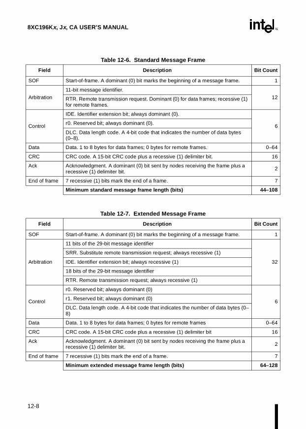
8XC196Kx, Jx, CA USER’S MANUAL
12-8
Table 12-6. Standard Message Frame
Field Description Bit Count
SOF Start-of-frame. A dominant (0) bit marks the beginning of a message frame. 1
Arbitration
11-bit message identifier.
12RTR. Remote transmission request. Dominant (0) for data frames; recessive (1) for remote frames.
Control
IDE. Identifier extension bit; always dominant (0).
6r0. Reserved bit; always dominant (0).
DLC. Data length code. A 4-bit code that indicates the number of data bytes (0–8).
Data Data. 1 to 8 bytes for data frames; 0 bytes for remote frames. 0–64
CRC CRC code. A 15-bit CRC code plus a recessive (1) delimiter bit. 16
Ack Acknowledgment. A dominant (0) bit sent by nodes receiving the frame plus a recessive (1) delimiter bit. 2
End of frame 7 recessive (1) bits mark the end of a frame. 7
Minimum standard message frame length (bits) 44–108
Table 12-7. Extended Message Frame
Field Description Bit Count
SOF Start-of-frame. A dominant (0) bit marks the beginning of a message frame. 1
Arbitration
11 bits of the 29-bit message identifier
32
SRR. Substitute remote transmission request; always recessive (1)
IDE. Identifier extension bit; always recessive (1)
18 bits of the 29-bit message identifier
RTR. Remote transmission request; always recessive (1)
Control
r0. Reserved bit; always dominant (0)
6r1. Reserved bit; always dominant (0)
DLC. Data length code. A 4-bit code that indicates the number of data bytes (0–8)
Data Data. 1 to 8 bytes for data frames; 0 bytes for remote frames 0–64
CRC CRC code. A 15-bit CRC code plus a recessive (1) delimiter bit 16
Ack Acknowledgment. A dominant (0) bit sent by nodes receiving the frame plus a recessive (1) delimiter bit. 2
End of frame 7 recessive (1) bits mark the end of a frame. 7
Minimum extended message frame length (bits) 64–128
12-9
CAN SERIAL COMMUNICATIONS CONTROLLER
12.3.4 Error Detection and Management Logic
The CAN controller has several error detection mechanisms, including cyclical redundancychecking (CRC) and bit coding rules (stuffing and destuffing). The CAN controller generates aCRC code for transmitted messages and checks the CRC code of incoming messages. The CRCpolynomial has been optimized for control applications with short messages.
After five consecutive bits of equal value are transmitted, a bit with the opposite polarity is addedto the bit stream. This bit is called a stuff bit; by adding a transition, a stuff bit aids in synchroni-zation. All message fields are stuffed except the CRC delimiter, the acknowledgment field, andthe end-of-frame field.
Receiving nodes reject data from any message that is corrupted during transmission and send anerror message via the CAN bus. Transmitting nodes monitor the CAN bus for error messages andautomatically repeat a transmission if an error occurs. The following error types are detected:
• stuff error — more than 5 equal bits in a sequence have occurred in a part of a receivedmessage where this is not allowed
• form error — the fixed-format part of a received frame has the wrong format (for example,a reserved bit has the wrong value)
• acknowledgment error — this device transmitted a message, but it was not acknowledgedby another node on the CAN bus. (The transmit error counter stops incrementing after 128acknowledgment errors, so this error type does not cause a bus-off state.)
• bit 1 error — the CAN controller tried to send a recessive (logic 1) bit as part of atransmitted message (with the exception of the arbitration field), but the monitored CANbus value was dominant (logic 0)
• bit 0 error — the CAN controller tried to send a dominant (logic 0) bit as part of atransmitted message (with the exception of the arbitration field), but the monitored CANbus value was recessive (logic 1)
• CRC error — the CRC checksum received for an incoming message does not match theCRC value that the CAN controller calculated for the received data
The CAN status register indicates the type of the first transmission error that occurred on theCAN bus and whether an abnormal number of errors have occurred. Two counters (a receive errorcounter and a transmit error counter) track the number of errors. The status register’s warning bitis set when the receive or transmit error counter reaches 96; the bus-off bit is set when eithercounter reaches 256. If this occurs, the CAN controller isolates itself from the CAN bus (floatsthe TX pin). Software must clear the INIT bit in the control register (Figure 12-6 on page 12-13)to begin a bus-off recovery sequence.

8XC196Kx, Jx, CA USER’S MANUAL
12-10
12.3.5 Bit Timing
A message object consists of a series of bits transmitted in consecutive bit times. The CAN pro-tocol specifies a bit time composed of four separate, nonoverlapping time segments: a synchro-nization delay segment, a propagation delay segment, and two phase delay segments (Figure 12-4and Table 12-8). The CAN controller implements a bit time as three segments, combiningPROP_SEG and PHASE_SEG1 into tTSEG1 (Figure 12-5 and Table 12-9). This implementation isidentical to that of the 82527 CAN peripheral.
Figure 12-4. A Bit Time as Specified by the CAN Protocol
Table 12-8. CAN Protocol Bit Time Segments
Symbol Definition
SYNC_SEG The synchronization delay segment allows for synchronization of the various nodes on the bus. An edge is expected to lie within this segment.
PROP_SEG The propagation delay segment compensates for the physical delay times within the network. It is twice the sum of the signal’s propagation time on the bus line, the input comparator delay, and the output driver delay. The factor of two accounts for the requirement that all nodes monitor all bus transmissions for errors.
PHASE_SEG1 This segment compensates for edge phase errors. It can be lengthened or shortened by resynchronization.
PHASE_SEG2 This segment compensates for edge phase errors. It can be lengthened or shortened by resynchronization.
SYNC_SEG PROP_SEG PHASE_SEG2PHASE_SEG1
Sample Transmit
Nominal Bit Time
A2603-01

12-11
CAN SERIAL COMMUNICATIONS CONTROLLER
Figure 12-5. A Bit Time as Implemented in the CAN Controller
Table 12-9. CAN Controller Bit Time Segments
Symbol Definition
tSYNC_SEG This time segment is equivalent to SYNC_SEG in the CAN protocol. Its length is one time quantum.
tTSEG1 This time segment is equivalent to the sum of PROP_SEG and PHASE_SEG1 in the CAN protocol. Its length is specified by the TSEG1 field in bit timing register 1. To allow for resyn-chronization, the sample point can be moved (tTSEG1 or tTSEG2 can be shortened and the other lengthened) by 1 to 4 time quanta, depending on the programmed value of the SJW field in bit timing register 0.
The CAN controller samples the bus once or three times, depending on the value of the sampling mode (SPL) bit in bit timing register 0. In three-sample mode, the hardware lengthens tTSEG1 by 2 time quanta to allow time for the additional two bus samples. In this case, the “sample point” shown in Figure 12-5 is the time of the third sample; the first and second samples occur 2 and 1 time quanta earlier, respectively.
tTSEG2 This time segment is equivalent to PHASE_SEG2 in the CAN protocol. Its length is specified by the TSEG2 field in bit timing register 1. To allow for resynchronization, the sample point can be moved (tTSEG1 or tTSEG2 can be shortened and the other lengthened) by 1 to 4 time quanta, depending on the programmed value of the SJW field in bit timing register 0.
TSEG1
Sample Transmit
1 tq
Bit Time
(TSEG1 + 1)tq
t
A2602-01
TSEG2tSYNC _SEG
t
(TSEG2 + 1)tq

8XC196Kx, Jx, CA USER’S MANUAL
12-12
12.3.5.1 Bit Timing Equations
The bit timing equations of the integrated CAN controller are equivalent to those for the 82527CAN peripheral with the DSC bit in the CPU interface register set (system clock divided by two).The following equations show the timing calculations for the integrated CAN controller and the82527 CAN peripheral, respectively.
where:FOSC = the input clock frequency on the XTAL1 pin, in MHz
BRP = the value of the BRP bit in bit timing register 0
TSEG1 = the value of the TSEG1 field in bit timing register 0
TSEG2 = the value of the TSEG1 field in bit timing register 1
Table 12-10 defines the bit timing relationships of the CAN controller.
Table 12-10. Bit Timing Relationships
Timing Parameter Definition
tBITTIME tSYNC_SEG + tTSEG1 + tTSEG2
tXTAL1 input clock period on XTAL1 (50 ns at 20 MHz operation)
tq 2tXTAL1 × (BRP + 1), where BRP is a field in bit timing register 0 (valid values are 0–63)
tSYNC_SEG 1tq
tTSEG1 (TSEG1 + 1) × tq, where TSEG1 is a field in bit timing register 1 (valid values are 2–15)
tTSEG2 (TSEG2 + 1) × tq, where TSEG2 is a field in bit timing register 1 (valid values are 1–7)
tSJW (SJW + 1) × tq, where SJW is a field in bit timing register 0 (valid values are 0–3)
tPROP The portion of tTSEG1 that is equivalent to PROP_SEG as defined by the CAN protocol. Twice the maximum sum of the physical bus delay, input comparator delay, and output driver delay, rounded up to the nearest multiple of tq.
CAN Controller CAN bus frequencyFosc
2 BRP + 1( )× 3 TSEG1 TSEG2+ +( )×-------------------------------------------------------------------------------------------------------------=
82527 CAN bus frequencyFosc
DSC 1+( ) BRP + 1( )× 3 TSEG1 TSEG2+ +( )×---------------------------------------------------------------------------------------------------------------------------------------=

12-13
CAN SERIAL COMMUNICATIONS CONTROLLER
12.4 CONFIGURING THE CAN CONTROLLER
This section explains how to configure the CAN controller. Several registers combine to controlthe configuration: the CAN control register, the two bit timing registers, and the three mask reg-isters.
12.4.1 Programming the CAN Control (CAN_CON) Register
The CAN control register (Figure 12-6) controls write access to the bit timing registers, enablesand disables global interrupt sources (error, status change, and individual message object), andcontrols access to the CAN bus.
CAN_CON (87C196CA)
Address:Reset State:
1E00H01H
Program the CAN control (CAN_CON) register to control write access to the bit timing registers, to enable and disable CAN interrupts, and to control access to the CAN bus.
7 0
87C196CA — CCE — — EIE SIE IE INIT
BitNumber
BitMnemonic Function
7 — Reserved; for compatibility with future devices, write zero to this bit.
6 CCE Change Configuration Enable
This bit controls whether software can write to the bit timing registers.
1 = allow write access 0 = prohibit write access
5:4 — Reserved; for compatibility with future devices, write zeros to these bits.
3 EIE Error Interrupt Enable
This bit enables and disables the bus-off and warn interrupts.
1 = enable bus-off and warn interrupts 0 = disable bus-off and warn interrupts
2 SIE Status-change Interrupt Enable
This bit enables and disables the successful reception (RXOK), successful transmission (TXOK), and error code change (LEC2:0) interrupts.
1 = enable status-change interrupt 0 = disable status-change interrupt
When the SIE bit is set, the CAN controller generates a successful reception (RXOK) interrupt request each time it receives a valid message, even if no message object accepts it.
Figure 12-6. CAN Control (CAN_CON) Register
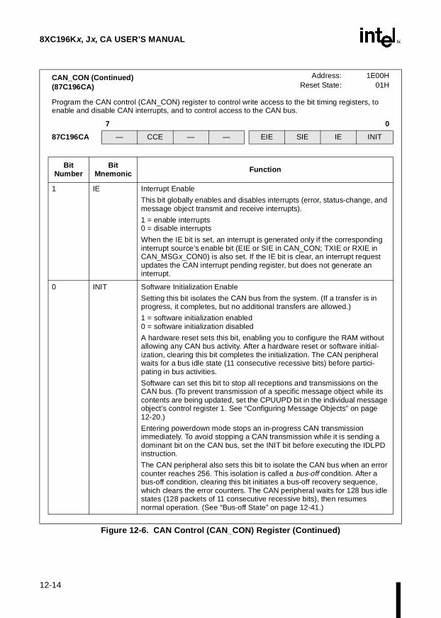
8XC196Kx, Jx, CA USER’S MANUAL
12-14
1 IE Interrupt Enable
This bit globally enables and disables interrupts (error, status-change, and message object transmit and receive interrupts).
1 = enable interrupts 0 = disable interrupts
When the IE bit is set, an interrupt is generated only if the corresponding interrupt source’s enable bit (EIE or SIE in CAN_CON; TXIE or RXIE in CAN_MSGx_CON0) is also set. If the IE bit is clear, an interrupt request updates the CAN interrupt pending register, but does not generate an interrupt.
0 INIT Software Initialization Enable
Setting this bit isolates the CAN bus from the system. (If a transfer is in progress, it completes, but no additional transfers are allowed.)
1 = software initialization enabled0 = software initialization disabled
A hardware reset sets this bit, enabling you to configure the RAM without allowing any CAN bus activity. After a hardware reset or software initial-ization, clearing this bit completes the initialization. The CAN peripheral waits for a bus idle state (11 consecutive recessive bits) before partici-pating in bus activities.
Software can set this bit to stop all receptions and transmissions on the CAN bus. (To prevent transmission of a specific message object while its contents are being updated, set the CPUUPD bit in the individual message object’s control register 1. See “Configuring Message Objects” on page 12-20.)
Entering powerdown mode stops an in-progress CAN transmission immediately. To avoid stopping a CAN transmission while it is sending a dominant bit on the CAN bus, set the INIT bit before executing the IDLPD instruction.
The CAN peripheral also sets this bit to isolate the CAN bus when an error counter reaches 256. This isolation is called a bus-off condition. After a bus-off condition, clearing this bit initiates a bus-off recovery sequence, which clears the error counters. The CAN peripheral waits for 128 bus idle states (128 packets of 11 consecutive recessive bits), then resumes normal operation. (See “Bus-off State” on page 12-41.)
CAN_CON (Continued)(87C196CA)
Address:Reset State:
1E00H01H
Program the CAN control (CAN_CON) register to control write access to the bit timing registers, to enable and disable CAN interrupts, and to control access to the CAN bus.
7 0
87C196CA — CCE — — EIE SIE IE INIT
BitNumber
BitMnemonic Function
Figure 12-6. CAN Control (CAN_CON) Register (Cont inued)

12-15
CAN SERIAL COMMUNICATIONS CONTROLLER
12.4.2 Programming the Bit Timing 0 (CAN_BTIME0) Register
Bit timing register 0 (Figure 12-7) defines the length of one time quantum and the maximumamount by which the sample point can be moved (tTSEG1 or tTSEG2 can be shortened and the otherlengthened) to compensate for resynchronization.
CAN_BTIME0(87C196CA)
Address:Reset State:
1E3FHUnchanged
Program the CAN bit timing 0 (CAN_BTIME0) register to define the length of one time quantum and the maximum number of time quanta by which a bit time can be modified for resynchronization.
7 0
87C196CA SJW1 SJW0 BRP5 BRP4 BRP3 BRP2 BRP1 BRP0
BitNumber
BitMnemonic Function
7:6 SJW1:0 Synchronization Jump Width
This field defines the maximum number of time quanta by which a resyn-chronization can modify tTSEG1 and tTSEG2. Valid programmed values are 0–3. The hardware adds 1 to the programmed value, so a “1” value causes the CAN peripheral to add or subtract 2 time quanta, for example. This adjustment has no effect on the total bit time; if tTSEG1 is increased by 2 tq, tTSEG2 is decreased by 2 tq, and vice versa.
5:0 BRP5:0 Baud-rate Prescaler
This field defines the length of one time quantum (tq), using the following formula, where tXTAL1 is the input clock period on XTAL1. Valid programmed values are 0–63.
For example, at 20 MHz operation, the system clock period is 50 ns. Writing 3 to BRP achieves a time quanta of 400 ns; writing 1 to BRP achieves a time quanta of 200 ns.
NOTE: The CCE bit (CAN_CON.6) must be set to enable write access to this register.
Figure 12-7. CAN Bit Timing 0 (CAN_BTIME0) Register
tq 2tXTAL1 BRP 1+( )×=
tq 2 50×( ) 3 1+( )× 400 ns= =
tq 2 50×( ) 1 1+( )× 200 ns= =

8XC196Kx, Jx, CA USER’S MANUAL
12-16
12.4.3 Programming the Bit Timing 1 (CAN_BTIME1) Register
Bit timing register 1 (Figure 12-8) controls the time at which the bus is sampled and the numberof samples taken. In single-sample mode, the bus is sampled once and the value of that sample isconsidered valid. In three-sample mode, the bus is sampled three times and the value of the ma-jority of those samples is considered valid. Single-sample mode may achieve a faster transmis-sion rate, but it is more susceptible to errors caused by noise on the CAN bus. Three-sample modeis less susceptible to noise-related errors, but it may be slower. If you specify three-sample mode,the hardware adds two time quanta to the TSEG1 value to allow time for two additional samplesduring tTSEG1.
CAN_BTIME1(87C196CA)
Address:Reset State:
1E4FHUnchanged
Program the CAN bit timing 1 (CAN_BTIME1) register to define the sample time and the sample mode. The CAN controller samples the bus during the last one (in single-sample mode) or three (in three-sample mode) time quanta of tTSEG1, and initiates a transmission at the end of tTSEG2. Therefore, specifying the lengths of tTSEG1 and tTSEG2 defines both the sample point and the trans-mission point.
7 0
87C196CA SPL TSEG2.2 TSEG2.1 TSEG2.0 TSEG1.3 TSEG1.2 TSEG1.1 TSEG1.0
BitNumber
BitMnemonic Function
7 SPL Sampling Mode
This bit determines how many samples are taken to determine a valid bit value.
1 = 3 samples, using majority logic0 = 1 sample
6:4 TSEG2 Time Segment 2
This field determines the length of time that follows the sample point within a bit time. Valid programmed values are 1–7; the hardware adds 1 to this value. (Note 2)
Figure 12-8. CAN Bit Timing 1 (CAN_BTIME1) Register

12-17
CAN SERIAL COMMUNICATIONS CONTROLLER
3:0 TSEG1 Time Segment 1
This field defines the length of time that precedes the sample point within a bit time. Valid programmed values are 2–15; the hardware adds 1 to this value. In three-sample mode, the hardware adds 2 time quanta to allow time for the two additional samples. (Note 2)
NOTES:1. The CCE bit (CAN_CON.6) must be set to enable write access to this register.2. For correct operation according to the CAN protocol, the total bit time must be at least 8 time
quanta, so the sum of the programmed values of TSEG1 and TSEG2 must be at least 5. (Thetotal bit time is the sum of tSYNC_SEG + tTSEG1 + tTSEG2. The length of tSYNC_SEG is 1 time quanta,and the hardware adds 1 to both TSEG1 and TSEG2. Therefore, if TSEG1 + TSEG2 = 5, thetotal bit length will be equal to 8 (1+5+1+1)). Table 12-11 lists additional conditions that must bemet to maintain synchronization.
Table 12-11. Bit Timing Requirements for Synchronization
Bit Time Segment Requirement Comments
tTSEG1
≥ 3tq minimum tolerance with 1tq propagation delay allowance
≥ tSJW + tPROP for single-sample mode
≥ tSJW + tPROP + 2tq for three-sample mode
tTSEG2 ≥ 2tq minimum tolerance
≥ tSJW if tSJW > tTSEG2 , sampling may occur after the bit time
CAN_BTIME1(87C196CA)
Address:Reset State:
1E4FHUnchanged
Program the CAN bit timing 1 (CAN_BTIME1) register to define the sample time and the sample mode. The CAN controller samples the bus during the last one (in single-sample mode) or three (in three-sample mode) time quanta of tTSEG1, and initiates a transmission at the end of tTSEG2. Therefore, specifying the lengths of tTSEG1 and tTSEG2 defines both the sample point and the trans-mission point.
7 0
87C196CA SPL TSEG2.2 TSEG2.1 TSEG2.0 TSEG1.3 TSEG1.2 TSEG1.1 TSEG1.0
BitNumber
BitMnemonic Function
Figure 12-8. CAN Bit Timing 1 (CAN_BTIME1) Register (Continued)

8XC196Kx, Jx, CA USER’S MANUAL
12-18
12.4.4 Programming a Message Acceptance Filter
The mask registers provide a method for developing an acceptance filtering strategy. Without afiltering strategy, a message object could accept an incoming message only if their identifierswere identical. The mask registers allow a message object to ignore one or more bits of incomingmessage identifiers, so it can accept a range of message identifiers.
The standard global mask register (Figure 12-9) applies to messages with standard (11-bit) mes-sage identifiers, while the extended global mask register (Figure 12-10) applies to messages withextended (29-bit) identifiers. The message 15 mask register (Figure 12-11) provides an additionalfilter for message object 15, to allow it to accept a greater range of message identifiers than mes-sage objects 1–14 can. Clear a mask bit to accept either a zero or a one in that position.
The CAN controller applies the appropriate global mask to each incoming message identifier andchecks for an acceptance match on message objects 1–14. If no match exists, it then applies themessage 15 mask and checks for a match on message object 15.
CAN_SGMSK(87C196CA)
Address:Reset State:
1E07H, 1E06HUnchanged
Program the CAN standard global mask (CAN_SGMSK) register to mask (“don’t care”) specific message identifier bits for standard message objects.
15 8
87C196CA MSK20 MSK19 MSK18 — — — — —
7 0
MSK28 MSK27 MSK26 MSK25 MSK24 MSK23 MSK22 MSK21
BitNumber
Bit Mnemonic Function
15:13 MSK20:18 ID Mask
These bits individually mask incoming message identifier (ID) bits.
0 = mask the ID bit (accept either “0” or “1”)1 = accept only an exact match
12:8 — Reserved; for compatibility with future devices, write zeros to these bits.
7:0 MSK28:21 ID Mask
These bits individually mask incoming message identifier (ID) bits.
0 = mask the ID bit (accept either “0” or “1”)1 = accept only an exact match
Figure 12-9. CAN Standard Global Mask (CAN_SGMSK) Register

12-19
CAN SERIAL COMMUNICATIONS CONTROLLER
CAN_EGMSK(87C196CA)
Address:
Reset State:
1E0BH, 1E0AH, 1E09H, 1E08HUnchanged
Program the CAN extended global mask (CAN_EGMSK) register to mask (“don’t care”) specific message identifier bits for extended message objects.
31 24
87C196CA MSK4 MSK3 MSK2 MSK1 MSK0 — — —
23 16
MSK12 MSK11 MSK10 MSK9 MSK8 MSK7 MSK6 MSK5
15 8
MSK20 MSK19 MSK18 MSK17 MSK16 MSK15 MSK14 MSK13
7 0
MSK28 MSK27 MSK26 MSK25 MSK24 MSK23 MSK22 MSK21
BitNumber
BitMnemonic Function
31:27 MSK4:0 ID Mask
These bits individually mask incoming message identifier (ID) bits.
0 = mask the ID bit (accept either “0” or “1”)1 = accept only an exact match
26:24 — Reserved; for compatibility with future devices, write zeros to these bits.
23:1615:87:0
MSK12:5MSK20:13MSK28:21
ID Mask
These bits individually mask incoming message identifier (ID) bits.
0 = mask the ID bit (accept either “0” or “1”)1 = accept only an exact match
Figure 12-10. CAN Extended Global Mask (CAN_EGMSK) Register
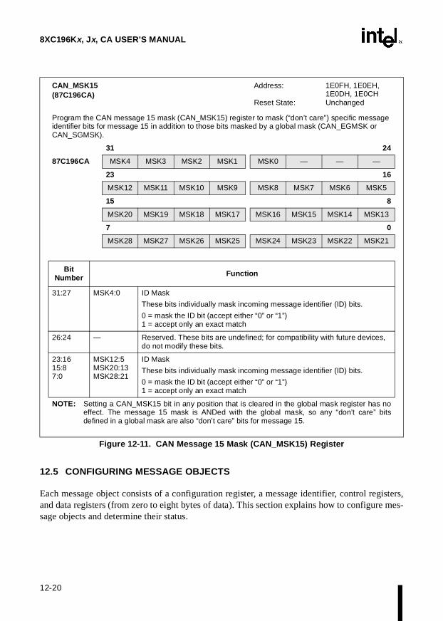
8XC196Kx, Jx, CA USER’S MANUAL
12-20
12.5 CONFIGURING MESSAGE OBJECTS
Each message object consists of a configuration register, a message identifier, control registers,and data registers (from zero to eight bytes of data). This section explains how to configure mes-sage objects and determine their status.
CAN_MSK15(87C196CA)
Address:
Reset State:
1E0FH, 1E0EH, 1E0DH, 1E0CHUnchanged
Program the CAN message 15 mask (CAN_MSK15) register to mask (“don’t care”) specific message identifier bits for message 15 in addition to those bits masked by a global mask (CAN_EGMSK or CAN_SGMSK).
31 24
87C196CA MSK4 MSK3 MSK2 MSK1 MSK0 — — —
23 16
MSK12 MSK11 MSK10 MSK9 MSK8 MSK7 MSK6 MSK5
15 8
MSK20 MSK19 MSK18 MSK17 MSK16 MSK15 MSK14 MSK13
7 0
MSK28 MSK27 MSK26 MSK25 MSK24 MSK23 MSK22 MSK21
BitNumber Function
31:27 MSK4:0 ID Mask
These bits individually mask incoming message identifier (ID) bits.
0 = mask the ID bit (accept either “0” or “1”)1 = accept only an exact match
26:24 — Reserved. These bits are undefined; for compatibility with future devices, do not modify these bits.
23:1615:87:0
MSK12:5MSK20:13MSK28:21
ID Mask
These bits individually mask incoming message identifier (ID) bits.
0 = mask the ID bit (accept either “0” or “1”)1 = accept only an exact match
NOTE: Setting a CAN_MSK15 bit in any position that is cleared in the global mask register has noeffect. The message 15 mask is ANDed with the global mask, so any “don’t care” bitsdefined in a global mask are also “don’t care” bits for message 15.
Figure 12-11. CAN Message 15 Mask (CAN_MSK15) Register
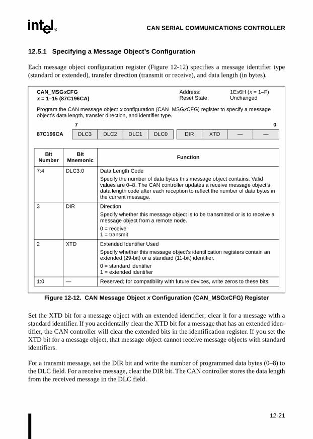
12-21
CAN SERIAL COMMUNICATIONS CONTROLLER
12.5.1 Specifying a Message Object’s Configuration
Each message object configuration register (Figure 12-12) specifies a message identifier type(standard or extended), transfer direction (transmit or receive), and data length (in bytes).
Set the XTD bit for a message object with an extended identifier; clear it for a message with astandard identifier. If you accidentally clear the XTD bit for a message that has an extended iden-tifier, the CAN controller will clear the extended bits in the identification register. If you set theXTD bit for a message object, that message object cannot receive message objects with standardidentifiers.
For a transmit message, set the DIR bit and write the number of programmed data bytes (0–8) tothe DLC field. For a receive message, clear the DIR bit. The CAN controller stores the data lengthfrom the received message in the DLC field.
CAN_MSGxCFGx = 1–15 (87C196CA)
Address:Reset State:
1Ex6H (x = 1–F)Unchanged
Program the CAN message object x configuration (CAN_MSGxCFG) register to specify a message object’s data length, transfer direction, and identifier type.
7 0
87C196CA DLC3 DLC2 DLC1 DLC0 DIR XTD — —
BitNumber
BitMnemonic Function
7:4 DLC3:0 Data Length Code
Specify the number of data bytes this message object contains. Valid values are 0–8. The CAN controller updates a receive message object’s data length code after each reception to reflect the number of data bytes in the current message.
3 DIR Direction
Specify whether this message object is to be transmitted or is to receive a message object from a remote node.
0 = receive1 = transmit
2 XTD Extended Identifier Used
Specify whether this message object’s identification registers contain an extended (29-bit) or a standard (11-bit) identifier.
0 = standard identifier1 = extended identifier
1:0 — Reserved; for compatibility with future devices, write zeros to these bits.
Figure 12-12. CAN Message Object x Configuration (CAN_MSGxCFG) Register

8XC196Kx, Jx, CA USER’S MANUAL
12-22
12.5.2 Programming the Message Object Identifier
For messages with extended identifiers, write the identifier to bits ID28:0. For messages withstandard identifiers, write the identifier to bits ID28:18. Software can change the identifier duringnormal operation without requiring a subsequent device reset. Clear the MSGVAL bit in the cor-responding message control register 0 to prevent the CAN controller from accessing the messageobject while the modification takes place, then set the bit to allow access.
CAN_MSGxID0–3x = 1–15 (87C196CA)
Address:
Reset State:
1Ex5H, 1Ex4H, 1Ex3H, 1Ex2H(x = 1–F)Unchanged
Write the message object’s identifier to the CAN message object x identifier (CAN_MSGxID0–3) register. Software can change the identifier during normal operation. Clear the MSGVAL bit in the corresponding CAN_MSGxCON0 register to prevent the CPU from accessing the message object, change the identifier in CAN_MSGxID0–3, then set the MSGVAL bit to allow access.
87C196CA 31 24
CAN_MSGxID3 ID4 ID3 ID2 ID1 ID0 — — —
23 16
CAN_MSGxID2 ID12 ID11 ID10 ID9 ID8 ID7 ID6 ID5
15 8
CAN_MSGxID1 ID20 ID19 ID18 ID17 ID16 ID15 ID14 ID13
7 0
CAN_MSGxID0 ID28 ID27 ID26 ID25 ID24 ID23 ID22 ID21
BitNumber
Bit Mnemonic Function
31:2723:1612:8
ID4:0ID12:5ID17:13
Message Identifier 17:0
These bits hold the 18 least-significant bits of an extended identifier. If you write an extended identifier to these bits, but specify a standard identifier (XTD = 0) in the corresponding message object’s configuration register (CAN_MSGxCFG), the CPU clears these bits (ID17:0).
26:24 — Reserved; for compatibility with future devices, write zeros to these bits.
15:137:0
ID20:18ID28:21
Message Identifier 28:18
These bits hold either an entire standard identifier or the 11 most-significant bits of an extended identifier.
NOTE: This register is the same as the arbitration register in the standalone 82527 CAN peripheral.
Figure 12-13. CAN Message Object x Identifier (CAN_MSG xID0–3) Register

12-23
CAN SERIAL COMMUNICATIONS CONTROLLER
12.5.3 Programming the Message Object Control Registers
Each message object control register consists of four bit pairs — one bit of each pair is in trueform and one is in complement form. This format allows software to set or clear any bit with asingle write operation, without affecting the remaining bits. Table 12-12 shows how to interpretthe bit-pair values.
12.5.3.1 Message Object Cont rol Register 0
Message object control register 0 (Figure 12-14) indicates whether an interrupt is pending, con-trols whether a successful transmission or reception generates an interrupt, and indicates whethera message object is ready to transmit.
12.5.3.2 Message Object Cont rol Register 1
Message object control register 1 (Figure 12-15) indicates whether the message object containsnew data, whether a message has been overwritten, whether the message is being updated, andwhether a transmission or reception is pending. Message objects 1–14 have only a single buffer,so if a second message is received before the CPU reads the first, the first message is overwritten.Message object 15 has two alternating buffers, so it can receive a second message while the firstis being processed. However, if a third message is received while the CPU is reading the first, thesecond message is overwritten.
12.5.4 Programming the Message Object Data
Each message object can have from zero to eight bytes of data. For transmit message objects,write the message data to the data registers (Figure 12-16). For receive message objects, the CANcontroller stores the received data in these registers. The CAN controller writes random values toany unused data bytes during operation, so you should not use unused data bytes as scratch-padmemory.
Table 12-12. Control Register Bit-pair Interpretation
Access Type MSB LSB Definition
Write
0 0 Not allowed (indeterminate)
0 1 Clear (0)
1 0 Set (1)
1 1 No change
Read0 1 Clear (0)
1 0 Set (1)

8XC196Kx, Jx, CA USER’S MANUAL
12-24
CAN_MSGxCON0 x = 1–15 (87C196CA)
Address:Reset State:
1Ex0H (x = 1–F)Unchanged
Program the CAN message object x control 0 (CAN_MSGxCON0) register to indicate whether the message object is ready to transmit and to control whether a successful transmission or reception generates an interrupt. The least-significant bit-pair indicates whether an interrupt is pending.
This register consists of four bit-pairs — the most-significant bit of each pair is in true form and the least-significant bit is in complement form. This format allows software to set or clear any bit with a single write operation, without affecting the remaining bits.
7 0
87C196CA MSGVAL MSGVAL TXIE TXIE RXIE RXIE INT_PND INT_PND
BitNumber
BitMnemonic Function
7:6 MSGVAL Message Object Valid
Set this bit-pair to indicate that a message object is valid (configured and ready for transmission or reception).
bit 7 bit 60 1 not ready1 0 message object is valid
The CAN peripheral will access a message object only if this bit-pair indicates that the message is valid. If multiple message objects have the same identifier, only one can be valid at any given time.
During initialization, software should clear this bit for any unused message objects. Software can clear this bit if a message is no longer needed or if you need to change a message object’s contents or identifier.
5:4 TXIE Transmit Interrupt Enable
Receive message objects do not use this bit-pair.
For transmit message objects, set this bit-pair to enable the CAN peripheral to initiate a transmit (TX) interrupt after a successful trans-mission. You must also set the interrupt enable bit (CAN_CON.1) to enable the interrupt.
bit 5 bit 40 1 no interrupt1 0 generate an interrupt
Figure 12-14. CAN Message Object x Control 0 (CAN_MSGxCON0) Register

12-25
CAN SERIAL COMMUNICATIONS CONTROLLER
3:2 RXIE Receive Interrupt Enable
Transmit message objects do not use this bit-pair.
For a receive message object, set this bit-pair to enable this message object to initiate a receive (RX) interrupt after a successful reception. You must also set the interrupt enable bit (CAN_CON.1) to enable the interrupt.
bit 3 bit 20 1 no interrupt1 0 generate an interrupt
1:0 INT_PND Interrupt Pending
This bit-pair indicates that this message object has initiated a transmit (TX) or receive (RX) interrupt. Software must clear this bit when it services the interrupt.
bit 1 bit 00 1 no interrupt1 0 an interrupt was generated
CAN_MSGxCON0 (Continued)x = 1–15 (87C196CA)
Address:Reset State:
1Ex0H (x = 1–F)Unchanged
Program the CAN message object x control 0 (CAN_MSGxCON0) register to indicate whether the message object is ready to transmit and to control whether a successful transmission or reception generates an interrupt. The least-significant bit-pair indicates whether an interrupt is pending.
This register consists of four bit-pairs — the most-significant bit of each pair is in true form and the least-significant bit is in complement form. This format allows software to set or clear any bit with a single write operation, without affecting the remaining bits.
7 0
87C196CA MSGVAL MSGVAL TXIE TXIE RXIE RXIE INT_PND INT_PND
BitNumber
BitMnemonic Function
Figure 12-14. CAN Message Object x Control 0 (CAN_MSGxCON0) Register (Continued)

8XC196Kx, Jx, CA USER’S MANUAL
12-26
CAN_MSGxCON1 x = 1–15 (87C196CA)
Address:Reset State:
1Ex1H (x = 1–F)Unchanged
The CAN message object x control 1 (CAN_MSGxCON1) register indicates whether a message object has been updated, whether a message has been overwritten, whether the CPU is updating the message, and whether a transmission or reception is pending.
This register consists of four bit-pairs — the most-significant bit of each pair is in true form and the least-significant bit is in complement form. This format allows software to set or clear any bit with a single write operation, without affecting the remaining bits.
7 0
87C196CA RMTPND RMTPND TX_REQ TX_REQ MSGLSTCPUUPD
MSGLSTCPUUPD
NEWDAT NEWDAT
BitNumber
BitMnemonic Function
7:6 RMTPND Remote Request Pending
Receive message objects do not use this bit-pair.
The CAN controller sets this bit-pair to indicate that a remote frame has requested the transmission of a transmit message object. If the CPUUPD bit-pair is clear, the CAN controller transmits the message object, then clears RMTPND. Setting RMTPND does not cause a transmission; it only indicates that a transmission is pending.
bit 7 bit 60 1 no pending request1 0 a remote request is pending
5:4 TX_REQ Transmission Request
Set this bit-pair to cause a receive message object to transmit a remote frame (a request for transmission) or to cause a transmit object to transmit a data frame. Read this bit-pair to determine whether a transmission is in progress.
bit 5 bit 40 1 no pending request; no transmission in progress1 0 transmission request; transmission in progress
Figure 12-15. CAN Message Object x Control 1 (CAN_MSG xCON1) Register

12-27
CAN SERIAL COMMUNICATIONS CONTROLLER
3:2 MSGLST orCPUUPD
Message Lost (receive)
For a receive message object, the CAN controller sets this bit-pair to indicate that it stored a new message while the NEWDAT bit-pair was still set, overwriting the previous message.
bit 3 bit 20 1 no overwrite occurred1 0 a message was lost (overwritten)
CPU Updating (transmit)
For a transmit message object, software should set this bit-pair to indicate that it is in the process of updating the message contents. This prevents a remote frame from triggering a transmission that would contain invalid data.
bit 3 bit 20 1 the message is valid1 0 software is updating data
1:0 NEWDAT New Data
This bit-pair indicates whether a message object is valid (configured and ready for transmission).
bit 1 bit 20 1 not ready1 0 message object is valid
For receive message objects, the CAN peripheral sets this bit-pair when it stores new data into the message object.
For transmit message objects, set this bit-pair and clear the CPUUPD bit-pair to indicate that the message contents have been updated. Clearing CPUUPD prevents a remote frame from triggering a transmission that would contain invalid data.
During initialization, clear this bit for any unused message objects.
CAN_MSGxCON1 (Continued)x = 1–15 (87C196CA)
Address:Reset State:
1Ex1H (x = 1–F)Unchanged
The CAN message object x control 1 (CAN_MSGxCON1) register indicates whether a message object has been updated, whether a message has been overwritten, whether the CPU is updating the message, and whether a transmission or reception is pending.
This register consists of four bit-pairs — the most-significant bit of each pair is in true form and the least-significant bit is in complement form. This format allows software to set or clear any bit with a single write operation, without affecting the remaining bits.
7 0
87C196CA RMTPND RMTPND TX_REQ TX_REQMSGLSTCPUUPD
MSGLSTCPUUPD NEWDAT NEWDAT
BitNumber
BitMnemonic Function
Figure 12-15. CAN Message Object x Control 1 (CAN_MSG xCON1) Register (Continued)

8XC196Kx, Jx, CA USER’S MANUAL
12-28
CAN_MSGxDATA0–7x = 1–15 (87C196CA)
Address:
Reset State:
1ExEH, 1ExDH, 1ExCH, 1ExBH, 1ExAH, 1Ex9H, 1Ex8H, 1Ex7H(x = 1–F)Unchanged
The CAN message object data (CAN_MSGxDATA0–7) registers contain data to be transmitted or data received. Any unused data bytes have random values that change during operation.
87C196CA 7 0
CAN_MSGxDATA7 Data 7
7 0
CAN_MSGxDATA6 Data 6
7 0
CAN_MSGxDATA5 Data 5
7 0
CAN_MSGxDATA4 Data 4
7 0
CAN_MSGxDATA3 Data 3
7 0
CAN_MSGxDATA2 Data 2
7 0
CAN_MSGxDATA1 Data 1
7 0
CAN_MSGxDATA0 Data 0
BitNumber Function
7:0 Data
Each message object can use from zero to eight data registers to hold data to be transmitted or data received.
For receive message objects, these registers accept data during a reception.
For transmit message objects, write the data that is to be transmitted to these registers. The number of data bytes must match the DLC field in the CAN_MSGxCFG register. (For example, if CAN_MSG1DATA0, CAN_MSG1DATA1, CAN_MSG1DATA2, and CAN_MSG1DATA3 contain data, the DLC field in CAN_MSG1CFG must contain 04H.)
Figure 12-16. CAN Message Object Data (CAN_MSG xDATA0–7) Registers

12-29
CAN SERIAL COMMUNICATIONS CONTROLLER
12.6 ENABLING THE CAN INTERRUPTS
The CAN controller has a single interrupt input (INT13) to the interrupt controller. (Generally,PTS interrupt service is not useful for the CAN controller because the PTS cannot readily deter-mine the source of the CAN controller’s multiplexed interrupts.) To enable the CAN controller’sinterrupts, you must enable the interrupt source by setting the CAN bit in INT_MASK1 (see Ta-ble 12-2 on page 12-3) and globally enable interrupt servicing (by executing the EI instruction).In addition, you must set bits in the CAN control register (Figure 12-17) and the individual mes-sage objects’ control register 0 (Figure 12-18) to enable the individual interrupt sources withinthe CAN controller.
CAN_CON (87C196CA)
Address:Reset State:
1E00H01H
Program the CAN control (CAN_CON) register to control write access to the bit timing registers, to enable and disable CAN interrupts, and to control access to the CAN bus.
7 0
87C196CA — CCE — — EIE SIE IE INIT
BitNumber
BitMnemonic Function
7 — Reserved; for compatibility with future devices, write zero to this bit.
6 CCE Change Configuration Enable
5:4 — Reserved; for compatibility with future devices, write zeros to these bits.
3 EIE Error Interrupt Enable
This bit enables and disables the bus-off and warn interrupts.
1 = enable bus-off and warn interrupts 0 = disable bus-off and warn interrupts
2 SIE Status-change Interrupt Enable
This bit enables and disables the successful reception (RXOK), successful transmission (TXOK), and error code change (LEC2:0) interrupts.
1 = enable status-change interrupt 0 = disable status-change interrupt
When the SIE bit is set, the CAN controller generates a successful reception (RXOK) interrupt request each time it receives a valid message, even if no message object accepts it.
Figure 12-17. CAN Control ( CAN_CON) Regi ster
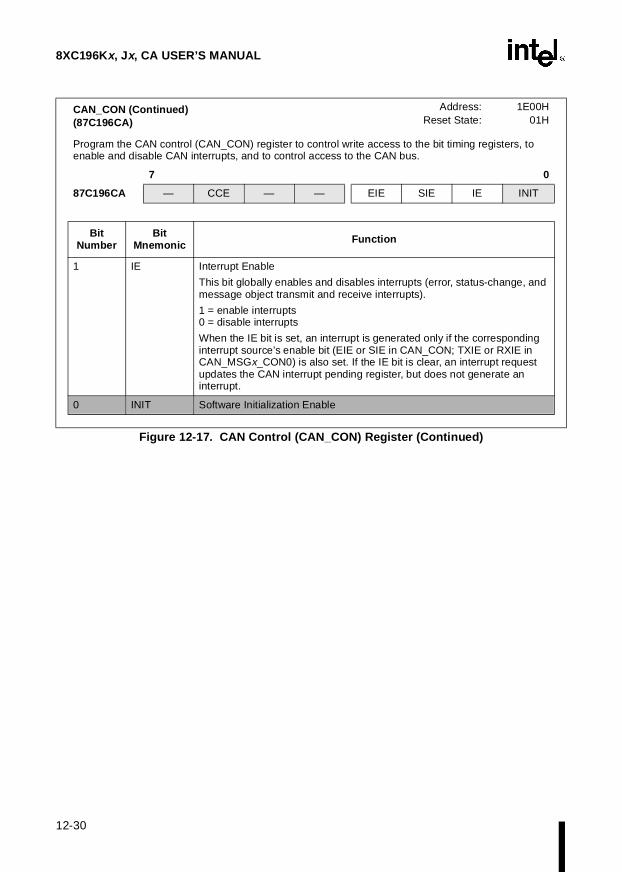
8XC196Kx, Jx, CA USER’S MANUAL
12-30
1 IE Interrupt Enable
This bit globally enables and disables interrupts (error, status-change, and message object transmit and receive interrupts).
1 = enable interrupts 0 = disable interrupts
When the IE bit is set, an interrupt is generated only if the corresponding interrupt source’s enable bit (EIE or SIE in CAN_CON; TXIE or RXIE in CAN_MSGx_CON0) is also set. If the IE bit is clear, an interrupt request updates the CAN interrupt pending register, but does not generate an interrupt.
0 INIT Software Initialization Enable
CAN_CON (Continued)(87C196CA)
Address:Reset State:
1E00H01H
Program the CAN control (CAN_CON) register to control write access to the bit timing registers, to enable and disable CAN interrupts, and to control access to the CAN bus.
7 0
87C196CA — CCE — — EIE SIE IE INIT
BitNumber
BitMnemonic Function
Figure 12-17. CAN Control (CAN_CON) Register (Continued)

12-31
CAN SERIAL COMMUNICATIONS CONTROLLER
When the SIE bit in the CAN control register is set, the CAN controller generates a successfulreception (RXOK) interrupt request each time it receives a valid message, even if no message ob-ject accepts it. If you set both the SIE bit (Figure 12-17) and an individual message object’s RXIEbit (Figure 12-18), the CAN controller generates two interrupt requests each time a message ob-ject receives a message. The status change interrupt is useful during development to detect buserrors caused by noise or other hardware problems. However, you should disable this interruptduring normal operation in most applications. If the status change interrupt is enabled, each statuschange generates an interrupt request, placing an unnecessary burden on the CPU. To prevent re-dundant interrupt requests, enable the error interrupt sources (with the EIE bit) and enable the re-ceive and transmit interrupts in the individual message objects.
CAN_MSGxCON0x = 1–15 (87C196CA)
Address:Reset State:
1Ex0H (x = 1–F)Unchanged
Program the CAN message object x control 0 (CAN_MSGxCON0) register to indicate whether the message object is ready to transmit and to control whether a successful transmission or reception generates an interrupt. The least-significant bit-pair indicates whether an interrupt is pending.
This register consists of four bit-pairs — the most-significant bit of each pair is in true form and the least-significant bit is in complement form. This format allows software to set or clear any bit with a single write operation, without affecting the remaining bits.
7 0
87C196CA MSGVAL MSGVAL TXIE TXIE RXIE RXIE INT_PND INT_PND
BitNumber
BitMnemonic Function
7:6 MSGVAL Message Object Valid
5:4 TXIE Transmit Interrupt Enable
Receive message objects do not use this bit-pair.
For transmit message objects, set this bit-pair to enable the CAN peripheral to initiate a transmit (TX) interrupt after a successful trans-mission. You must also set the interrupt enable bit (CAN_CON.1) to enable the interrupt.
bit 5 bit 40 1 no interrupt1 0 generate an interrupt
3:2 RXIE Receive Interrupt Enable
Transmit message objects do not use this bit-pair.
For receive message objects, set this bit-pair to enable the CAN peripheral to initiate a receive (RX) interrupt after a successful reception. You must also set the interrupt enable bit (CAN_CON.1) to enable the interrupt.
bit 3 bit 20 1 no interrupt1 0 generate an interrupt
1:0 INT_PND Interrupt Pending
Figure 12-18. CAN Message Object x Control 0 (CAN_MSGxCON0) Register

8XC196Kx, Jx, CA USER’S MANUAL
12-32
12.7 DETERMINING THE CAN CONTROLLER’S INTERRUPT STATUS
A successful reception or transmission or a change in the status register can cause the CAN con-troller to generate an interrupt request. The INT_PEND1 register (see Table 12-2 on page 12-3)indicates whether a CAN interrupt request is pending. The CAN interrupt pending register (Fig-ure 12-19) indicates the source of the request (either the status register or a specific message ob-ject). Your interrupt service routine should read the CAN_INT register to ensure that noadditional interrupts are pending before executing the return instruction. Chapter 5, “Standardand PTS Interrupts,” discusses interrupt service, relative priorities, and timing.
CAN_INTread-only (87C196CA)
Address:Reset State:
1E5FH00H
The CAN interrupt pending (CAN_INT) register indicates the source of the highest priority pending interrupt. If a status change generated the interrupt request, software can read the status register (CAN_STAT) to determine whether the interrupt request was caused by an abnormal error rate, a successful reception, a successful transmission, or a new error. If an individual message object generated the interrupt request, software can read the associated message object control 0 register (CAN_MSGxCON0). The INT_PND bit-pair will be set, indicating that a receive or transmit interrupt request is pending.
7 0
87C196CA Pending Interrupt
BitNumber Function
7:0 Pending Interrupt
This field indicates the source of the highest priority pending interrupt.
Value Pending Interrupt Priority (15 is highest; 0 is lowest)
00H none —01H status register 1502H message object 15 1403H message object 1 1304H message object 2 1205H message object 3 1106H message object 4 1007H message object 5 908H message object 6 809H message object 7 70AH message object 8 60BH message object 9 50CH message object 10 40DH message object 11 30EH message object 12 20FH message object 13 110H message object 14 0
Figure 12-19. CAN Interrupt Pending (CAN_INT) Register

12-33
CAN SERIAL COMMUNICATIONS CONTROLLER
If a status change generated the interrupt (CAN_INT = 01H), software can read the CAN statusregister (Figure 12-20) to determine the source of the interrupt request.
CAN_STAT(87C196CA)
Address:Reset State:
1E01HXXH
The CAN status (CAN_STAT) register reflects the current status of the CAN peripheral.
7 0
87C196CA BUSOFF WARN — RXOK TXOK LEC2 LEC1 LEC0
BitNumber
BitMnemonic Function
7 BUSOFF Bus-off Status
The CAN peripheral sets this read-only bit to indicate that it has isolated itself from the CAN bus (floated the TX pin) because an error counter has reached 256. A bus-off recovery sequence clears this bit and clears the error counters. (See “Bus-off State” on page 12-41.)
6 WARN Warning Status
The CAN peripheral sets this read-only bit to indicate that an error counter has reached 96, indicating an abnormal rate of errors on the CAN bus.
5 — Reserved. This bit is undefined.
4 RXOK Reception Successful
The CAN peripheral sets this bit to indicate that a message has been successfully received (error free, regardless of acknowledgment) since the bit was last cleared. Software must clear this bit when it services the interrupt.
3 TXOK Transmission Successful
The CAN peripheral sets this bit to indicate that a message has been successfully transmitted (error free and acknowledged by at least one other node) since the bit was last cleared. Software must clear this bit when it services the interrupt.
2:0 LEC2:0 Last Error Code
This field indicates the error type of the first error that occurs in a message frame on the CAN bus. (“Error Detection and Management Logic” on page 12-9 describes the error types.)
LEC2 LEC1 LEC0 Error Type0 0 0 no error0 0 1 stuff error0 1 0 form error0 1 1 acknowledgment error1 0 0 bit 1 error1 0 1 bit 0 error1 1 0 CRC error1 1 1 unused
Figure 12-20. CAN Status (CAN_STAT) Register

8XC196Kx, Jx, CA USER’S MANUAL
12-34
If an individual message object caused the interrupt request (CAN_INT = 02–10H), software canread the associated message object control 0 register (Figure 12-21). The INT_PND bit-pair willbe set, indicating that a receive or transmit interrupt request is pending.
CAN_MSGxCON0(n = 1–15)
Address: 1Ex0H (x=1–F)Reset State: Unchanged
Program the CAN message object x control 0 register (CAN_MSGxCON0) to indicate whether the message object is ready to transmit and to control whether a successful transmission or reception generates an interrupt. The most-significant bit-pair indicates whether an interrupt is pending.
This register consists of four bit-pairs — the most-significant bit of each pair is in true form and the least-significant bit is in complement form. This format allows software to set or clear any bit with a single write operation, without affecting the remaining bits.
7 0
MSGVAL MSGVAL TXIE TXIE RXIE RXIE INT_PND INT_PND
Bit Number
Bit Mnemonic Function
7:6 MSGVAL Message Object Valid
5:4 TXIE Transmit Interrupt Enable
3:2 RXIE Receive Interrupt Enable
1:0 INT_PND Interrupt Pending
This bit-pair indicates that the CAN peripheral has initiated a transmit (TX) or receive (RX) interrupt. Software must clear this bit when it services the interrupt.
01 = no interrupt 10 = an interrupt was generated
Figure 12-21. CAN Message Object x Control 0 (CAN_MSG xCON0) Register

12-35
CAN SERIAL COMMUNICATIONS CONTROLLER
12.8 FLOW DIAGRAMS
The flow diagrams in this section describe the steps that your software (shown as CPU) and theCAN controller execute to receive and transmit messages. Table 12-13 lists the register bitsshown in the diagrams along with their associated registers and a cross-reference to the figure thatdescribes them.
Table 12-13. Cross-reference for Register Bits Shown in Flowcharts
Bit Mnemonic Register Mnemonic Figure and Page
CPUUPD CAN_MSGxCON1 Figure 12-15 on page 12-26
DIR CAN_MSGxCFG Figure 12-12 on page 12-21
DLC CAN_MSGxCFG Figure 12-12 on page 12-21
ID CAN_MSGxID Figure 12-13 on page 12-22
INT_PND CAN_MSGxCON0 Figure 12-14 on page 12-24
MSGLST CAN_MSGxCON1 Figure 12-15 on page 12-26
MSGVAL CAN_MSGxCON0 Figure 12-14 on page 12-24
NEWDAT CAN_MSGxCON1 Figure 12-15 on page 12-26
RMTPND CAN_MSGxCON1 Figure 12-15 on page 12-26
RXIE CAN_MSGxCON0 Figure 12-14 on page 12-24
TXIE CAN_MSGxCON0 Figure 12-14 on page 12-24
TX_REG CAN_MSGxCON1 Figure 12-15 on page 12-26
XTD CAN_MSGxCFG Figure 12-12 on page 12-21
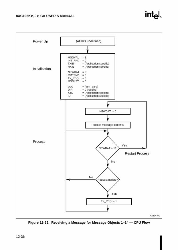
8XC196Kx, Jx, CA USER’S MANUAL
12-36
Figure 12-22. Receiving a Message for Message Objects 1–14 — CPU Flow
(All bits undefined)
NEWDAT := 0
Process message contents.
NEWDAT = 1?
Request update?
TX_REQ := 1
Power Up
Initialization
Process
Yes
No
No
Yes
Restart Process
A2594-01
MSGVAL INT_PND TXIE RXIE
:= 1 := 0 := (Application specific) := (Application specific)
NEWDAT RMTPND TX_REQ MSGLST
:= 0 := 0 := 0 := 0
DLC DIR XTD ID
:= (don't care) := 0 (receive) := (Application specific) := (Application specific)
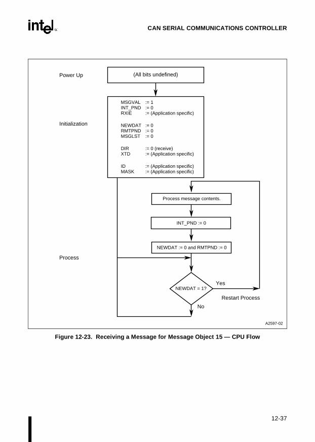
12-37
CAN SERIAL COMMUNICATIONS CONTROLLER
Figure 12-23. Receiving a Message for Message Object 15 — CPU Flow
(All bits undefined)
NEWDAT := 0 and RMTPND := 0
Process message contents.
NEWDAT = 1?
Power Up
Initialization
Process
No
Yes
Restart Process
A2597-02
MSGVAL INT_PND RXIE
:= 1 := 0 := (Application specific)
NEWDAT RMTPND MSGLST
:= 0 := 0 := 0
DIR XTD
:= 0 (receive) := (Application specific)
ID MASK
:= (Application specific) := (Application specific)
INT_PND := 0
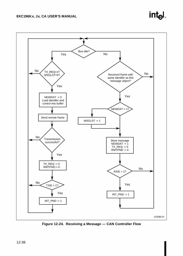
8XC196Kx, Jx, CA USER’S MANUAL
12-38
Figure 12-24. Receiving a Message — CAN Controller Flow
NEWDAT := 0 Load identifer and control into buffer
Send remote frame
Transmission successful?
TXIE = 1?
INT_PND := 1
TX_REQ := 0 RMTPND:= 0
TX_REQ=1? MSGLST=0?
Bus idle?
Received frame with same identifer as this
message object?
RXIE = 1?
INT_PND := 1
A2598-01
No
No
No
No
No
Yes
Yes
Yes
Yes
Yes
Yes No
NEWDAT = 1?
Store message NEWDAT := 1 TX_REQ := 0 RMTPND := 0
MSGLST := 1

12-39
CAN SERIAL COMMUNICATIONS CONTROLLER
Figure 12-25. Transmitting a Message — CPU Flow
(All bits undefined)
CPUUPD := 1 NEWDAT := 1
Want to send?
TX_REQ := 1
Power Up
Initialization
Update
Yes
No YesUpdate message?
CPUUPD := 0
Write/calculate message contents.
A2596-01
MSGVAL INT_PND TXIE RXIE
:= 1 := 0 := (Application specific) := (Application specific)
NEWDAT RMTPND TX_REQ MSGLST
:= 0 := 0 := 0 := 0
DLC DIR XTD
:= (Application specific) := 1 (transmit) := (Application specific)
ID := (Application specific)

8XC196Kx, Jx, CA USER’S MANUAL
12-40
Figure 12-26. Transmitting a Message — CAN Cont roller Flow
NEWDAT := 0 Load message
into buffer
Send message
Transmission successful?
NEWDAT = 1?
TXIE = 1?
INT_PND := 1
TX_REQ := 0 RMTPND := 0
TX_REQ= 1? CPUUPD= 0?
Bus free?
Received remote frame with same identifer as this message object?
TX_REQ := 1 RMTPND := 1
RXIE = 1?
INT_PND := 1
A2595-02
No
No
No
No
No
No
Yes
Yes
Yes
Yes
Yes
Yes
Yes No

12-41
CAN SERIAL COMMUNICATIONS CONTROLLER
12.9 DESIGN CONSIDERATIONS
This section outlines design considerations for the CAN controller.
12.9.1 Hardware Reset
A hardware reset clears the error management counters and the bus-off state and leaves the reg-isters with the values listed in Table 12-14.
12.9.2 Software Initialization
The software initialization state allows software to configure the CAN controller’s RAM withoutrisk of messages being received or transmitted during this time. Setting the INIT bit in the controlregister causes the CAN controller to enter the software initialization state. Either a hardware re-set or a software write can set the INIT bit. While INIT is set, all message transfers to and fromthe CAN controller are stopped and the error counters and bit timing registers are unchanged.Your software should clear the INIT bit to cause the CAN controller to exit the software initial-ization state. At this time, the CAN controller synchronizes itself to the CAN bus by waiting fora bus idle state (11 consecutive recessive bits) before participating in bus activities.
12.9.3 Bus-off State
If an error counter reaches 256, the CAN controller isolates itself from the CAN bus, sets theBUSOFF bit in the status register, and sets the INIT bit in the control register. While INIT is set,all message transfers to and from the CAN controller are stopped; the error counters and bit tim-ing registers are unchanged. Software must clear the INIT bit to initiate the bus-off recovery se-quence.
Table 12-14. Register Values Following Reset
Register Hex Address Reset Value
Control 1E00 01H
Status 1E01 undefined
Standard Global Mask 1E06–1E07 unchanged (undefined at power-up)
Extended Global Mask 1E08–1E0B unchanged (undefined at power-up)
Message 15 Mask 1E0C–1E0F unchanged (undefined at power-up)
Bit Timing 0 1E3F unchanged (undefined at power-up)
Bit Timing 1 1E4F unchanged (undefined at power-up)
Interrupt 1E5F 00H
Message Object x 1Ex0–1ExE unchanged (undefined at power-up)

8XC196Kx, Jx, CA USER’S MANUAL
12-42
The CAN controller synchronizes itself to the CAN bus by waiting for 128 bus idle states (128occurrences of 11 consecutive recessive bits) before participating in bus activities. During this se-quence, the CAN controller writes a bit 0 error code to the LEC2:0 bits of the status register eachtime it receives a recessive bit. Software can check the status register to determine whether theCAN bus is stuck in a dominant state. Once the CAN controller is resynchronized with the CANbus, it clears the BUSOFF bit and starts transferring messages again.
13Minimum Hardware Considerations

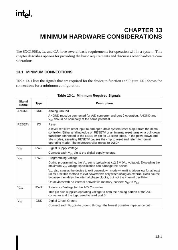
13-1
CHAPTER 13MINIMUM HARDWARE CONSIDERATIONS
The 8XC196Kx, Jx, and CA have several basic requirements for operation within a system. Thischapter describes options for providing the basic requirements and discusses other hardware con-siderations.
13.1 MINIMUM CONNECTIONS
Table 13-1 lists the signals that are required for the device to function and Figure 13-1 shows theconnections for a minimum configuration.
Table 13-1. Minimum Requi red Signals
SignalName Type Description
ANGND GND Analog Ground
ANGND must be connected for A/D converter and port 0 operation. ANGND and VSS should be nominally at the same potential.
RESET# I/O Reset
A level-sensitive reset input to and open-drain system reset output from the micro-controller. Either a falling edge on RESET# or an internal reset turns on a pull-down transistor connected to the RESET# pin for 16 state times. In the powerdown and idle modes, asserting RESET# causes the chip to reset and return to normal operating mode. The microcontroller resets to 2080H.
VCC PWR Digital Supply Voltage
Connect each VCC pin to the digital supply voltage.
VPP PWR Programming Voltage
During programming, the VPP pin is typically at +12.5 V (VPP voltage). Exceeding the maximum VPP voltage specification can damage the device.
VPP also causes the device to exit powerdown mode when it is driven low for at least 50 ns. Use this method to exit powerdown only when using an external clock source because it enables the internal phase clocks, but not the internal oscillator.
On devices with no internal nonvolatile memory, connect VPP to VCC.
VREF PWR Reference Voltage for the A/D Converter
This pin also supplies operating voltage to both the analog portion of the A/D converter and the logic used to read port 0.
VSS GND Digital Circuit Ground
Connect each VSS pin to ground through the lowest possible impedance path.

8XC196Kx, Jx, CA USER’S MANUAL
13-2
13.1.1 Unused Inputs
For predictable performance, it is important to tie unused inputs to VCC or VSS. Otherwise, theycan float to a mid-voltage level and draw excessive current. Unused interrupt inputs may generatespurious interrupts if left unconnected.
13.1.2 I/O Port Pin Connections
Tie unused input-only port inputs to VSS as shown in Figure 13-1. Chapter 6, “I/O Ports,” containsinformation about initializing and configuring the ports. Table 13-2 lists the sections, with pagenumbers, that contain the information for each port.
XTAL1 I Input Crystal/Resonator or External Clock Input
Input to the on-chip oscillator and the internal clock generators. The internal clock generators provide the peripheral clocks, CPU clock, and CLKOUT signal. When using an external clock source instead of the on-chip oscillator, connect the clock input to XTAL1. The external clock signal must meet the VIH specification for XTAL1 (see datasheet).
XTAL2 O Inverted Output for the Crystal/Resonator
Output of the on-chip oscillator inverter. Leave XTAL2 floating when the design uses a external clock source instead of the on-chip oscillator.
Table 13-2. I/O Port Configuration Guide
Port Where to Find Configuration Information
Port 0 “Standard Input-only Port Considerations” on page 6-3
Ports 1 and 2 “Bidirectional Port Pin Configurations” on page 6-10 and “Bidirectional Port Considerations” on page 6-12
Ports 3 and 4 “Bidirectional Ports 3 and 4 (Address/Data Bus) Operation” on page 6-16
Ports 5 and 6 “Bidirectional Port Pin Configurations” on page 6-10 and “Bidirectional Port Considerations” on page 6-12
Table 13-1. Minimum Required Signals(Continued)
SignalName Type Description

13-3
MINIMUM HARDWARE CONSIDERATIONS
Figure 13-1. Minimum Hardware Connections
ALE
ANGND
INST
XTAL1XTAL2
VCC (Note 2)0.01 µF
BUSWIDTH
NMI
READY
VCC
Port 5 / Bus Control (Note 4)
20 pF 20 pF(Note 1)
4.7 µF+
VCC+
1 µF
1 M
RESET#
BHE#
WR#
RD#
EA#
+1 µF
VCC
VCC
A2643-02
VSS
VPP
VREF
8XC196 Device
VCC
Notes: 1. See the datasheet for the oscillator frequency range (FOSC) and the crystal manufacturer's datasheet for recommended load capacitors. 2. The number of VCC and VSS pins varies with package type (see datasheet). Be sure to connect each VCC pin to the supply voltage and each VSS pin to ground. 3. Connect the RC network to VPP only if powerdown mode will be used. Otherwise, connect VPP to VCC. 4. No connection is required. 5. Tie all input-only port pins to VSS.
(Note 3)
Input-only Port Pins (Note 5)
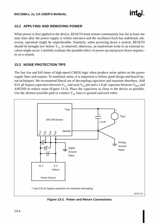
8XC196Kx, Jx, CA USER’S MANUAL
13-4
13.2 APPLYING AND REMOVING POWER
When power is first applied to the device, RESET# must remain continuously low for at least onestate time after the power supply is within tolerance and the oscillator/clock has stabilized; oth-erwise, operation might be unpredictable. Similarly, when powering down a system, RESET#should be brought low before VCC is removed; otherwise, an inadvertent write to an external lo-cation might occur. Carefully evaluate the possible effect of power-up and power-down sequenc-es on a system.
13.3 NOISE PROTECTION TIPS
The fast rise and fall times of high-speed CMOS logic often produce noise spikes on the powersupply lines and outputs. To minimize noise, it is important to follow good design and board lay-out techniques. We recommend liberal use of decoupling capacitors and transient absorbers. Add0.01 µF bypass capacitors between VCC and each VSS pin and a 1.0 µF capacitor between VREF andANGND to reduce noise (Figure 13-2). Place the capacitors as close to the device as possible.Use the shortest possible path to connect VSS lines to ground and each other.
Figure 13-2. Power and Return Connections
8XC196 Device
VREF
ANGND
+5 V 5 V
Return
Analog
Ground
Plane
Power Source
†
†
† Use 0.01 µF bypass capacitors for maximum decoupling.
Digital
Ground
Plane
+
1.0 µF
A0272-02
+
–
VREF
VC
C
VS
S
VS
S
VS
S
†
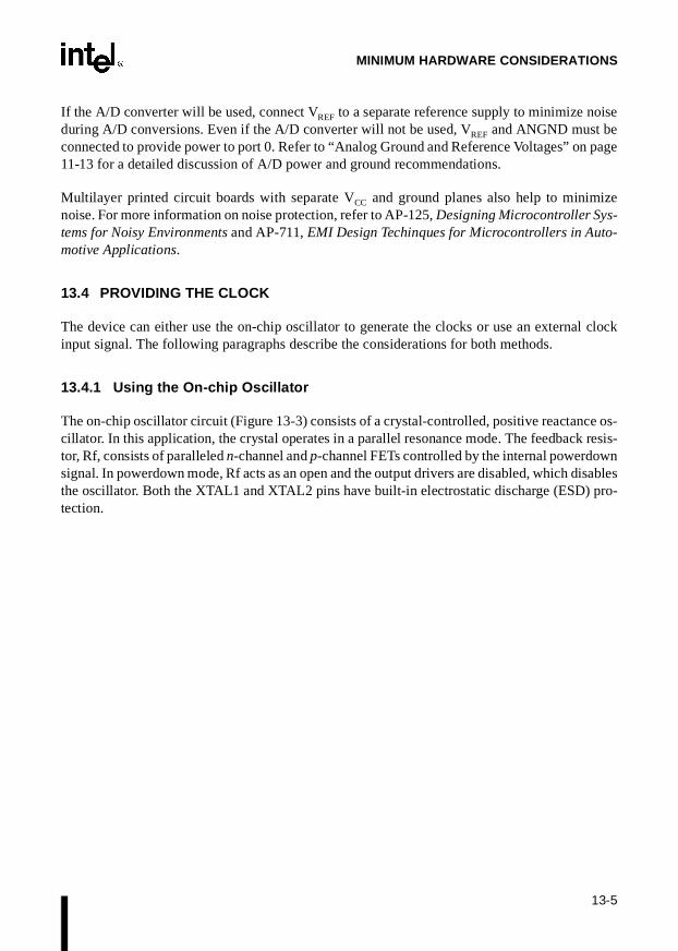
13-5
MINIMUM HARDWARE CONSIDERATIONS
If the A/D converter will be used, connect VREF to a separate reference supply to minimize noiseduring A/D conversions. Even if the A/D converter will not be used, VREF and ANGND must beconnected to provide power to port 0. Refer to “Analog Ground and Reference Voltages” on page11-13 for a detailed discussion of A/D power and ground recommendations.
Multilayer printed circuit boards with separate VCC and ground planes also help to minimizenoise. For more information on noise protection, refer to AP-125, Designing Microcontroller Sys-tems for Noisy Environments and AP-711, EMI Design Techinques for Microcontrollers in Auto-motive Applications.
13.4 PROVIDING THE CLOCK
The device can either use the on-chip oscillator to generate the clocks or use an external clockinput signal. The following paragraphs describe the considerations for both methods.
13.4.1 Using the On-chip Oscillator
The on-chip oscillator circuit (Figure 13-3) consists of a crystal-controlled, positive reactance os-cillator. In this application, the crystal operates in a parallel resonance mode. The feedback resis-tor, Rf, consists of paralleled n-channel and p-channel FETs controlled by the internal powerdownsignal. In powerdown mode, Rf acts as an open and the output drivers are disabled, which disablesthe oscillator. Both the XTAL1 and XTAL2 pins have built-in electrostatic discharge (ESD) pro-tection.
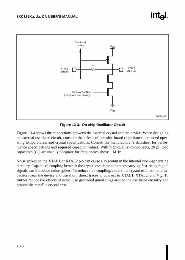
8XC196Kx, Jx, CA USER’S MANUAL
13-6
Figure 13-3. On-chip Oscillator Circuit
Figure 13-4 shows the connections between the external crystal and the device. When designingan external oscillator circuit, consider the effects of parasitic board capacitance, extended oper-ating temperatures, and crystal specifications. Consult the manufacturer’s datasheet for perfor-mance specifications and required capacitor values. With high-quality components, 20 pF loadcapacitors (CL) are usually adequate for frequencies above 1 MHz.
Noise spikes on the XTAL1 or XTAL2 pin can cause a miscount in the internal clock-generatingcircuitry. Capacitive coupling between the crystal oscillator and traces carrying fast-rising digitalsignals can introduce noise spikes. To reduce this coupling, mount the crystal oscillator and ca-pacitors near the device and use short, direct traces to connect to XTAL1, XTAL2, and VSS. Tofurther reduce the effects of noise, use grounded guard rings around the oscillator circuitry andground the metallic crystal case.
RfXTAL2 (Output)
VCC
XTAL1 (Input)
Oscillator Enable# (from powerdown circuitry)
To internal circuitry
A0076-03
VSS

13-7
MINIMUM HARDWARE CONSIDERATIONS
Figure 13-4. External Crystal Connections
13.4.2 Using a Ceramic Resonator Instead of a Crystal Oscillator
In cost-sensitive applications, you may choose to use a ceramic resonator instead of a crystal os-cillator. Ceramic resonators may require slightly different load capacitor values and circuit con-figurations. Consult the manufacturer’s datasheet for the required oscillator circuitry.
13.4.3 Providing an External Clock Source
To use an external clock source, apply a clock signal to XTAL1 and let XTAL2 float (Figure13-5). To ensure proper operation, the external clock source must meet the minimum high andlow times (TXHXX and TXLXX ) and the maximum rise and fall transition times (TXLHX and TXHXL)(Figure 13-6). The longer the rise and fall times, the higher the probability that external noise willaffect the clock generator circuitry and cause unreliable operation. See the datasheet for requiredXTAL1 voltage drive levels and actual specifications.
8XC196 Device
XTAL2
XTAL1
Quartz Crystal
C1
C2
A0273-02
Note: Mount oscillator components close to the device and use short, direct traces to XTAL1, XTAL2, and Vss. When using crystals, C1=C2≈20 pF. When using ceramic resonators, consult the manufacturer for recommended oscillator circuitry.
8XC196 Device
XTAL2
XTAL1
Quartz Crystal
C1
C2
A0273-02
Note: Mount oscillator components close to the device and use short, direct traces to XTAL1, XTAL2, and Vss. When using crystals, C1=C2≈20 pF. When using ceramic resonators, consult the manufacturer for recommended oscillator circuitry.
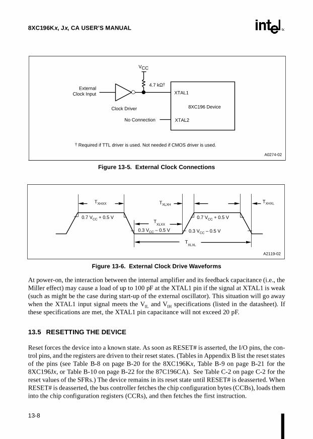
8XC196Kx, Jx, CA USER’S MANUAL
13-8
Figure 13-5. External Clock Connections
Figure 13-6. External Clock Drive Waveforms
At power-on, the interaction between the internal amplifier and its feedback capacitance (i.e., theMiller effect) may cause a load of up to 100 pF at the XTAL1 pin if the signal at XTAL1 is weak(such as might be the case during start-up of the external oscillator). This situation will go awaywhen the XTAL1 input signal meets the VIL and VIH specifications (listed in the datasheet). Ifthese specifications are met, the XTAL1 pin capacitance will not exceed 20 pF.
13.5 RESETTING THE DEVICE
Reset forces the device into a known state. As soon as RESET# is asserted, the I/O pins, the con-trol pins, and the registers are driven to their reset states. (Tables in Appendix B list the reset statesof the pins (see Table B-8 on page B-20 for the 8XC196Kx, Table B-9 on page B-21 for the8XC196Jx, or Table B-10 on page B-22 for the 87C196CA). See Table C-2 on page C-2 for thereset values of the SFRs.) The device remains in its reset state until RESET# is deasserted. WhenRESET# is deasserted, the bus controller fetches the chip configuration bytes (CCBs), loads theminto the chip configuration registers (CCRs), and then fetches the first instruction.
4.7 kن
8XC196 Device
XTAL2
XTAL1External
Clock Input
Clock Driver
No Connection
VCC
A0274-02
† Required if TTL driver is used. Not needed if CMOS driver is used.
4.7 kن
8XC196 Device
XTAL2
XTAL1External
Clock Input
Clock Driver
No Connection
VCC
A0274-02
† Required if TTL driver is used. Not needed if CMOS driver is used.
A2119-02
TXHXX
TXLXX
TXHXL
TXLXL
0.3 VCC – 0.5 V
0.7 VCC + 0.5 V
TXLXH
0.7 VCC + 0.5 V
0.3 VCC – 0.5 V

13-9
MINIMUM HARDWARE CONSIDERATIONS
Figure 13-7 shows the reset-sequence timing. Depending upon when RESET# is brought high,the CLKOUT signal may become out of phase with the PH1 internal clock. When this occurs, theclock generator immediately resynchronizes CLKOUT as shown in Case 2.
Figure 13-7. Reset Timing Sequence
The following events will reset the device (see Figure 13-8):
• an external device pulls the RESET# pin low
• the CPU issues the reset (RST) instruction
• the CPU issues an idle/powerdown (IDLPD) instruction with an illegal key operand
• the watchdog timer (WDT) overflows
• the oscillator fail detect (OFD) circuitry is enabled and an oscillator failure occurs
The following paragraphs describe each of these reset methods in more detail.
RESET# Pin
Case 1 CLKOUT
Case 2 CLKOUT
Internal Reset
ALE
CCB0 CCB1
Phases Resynchronized
RD#
AD7:0
Bus parameters defined by CCB0 (ready control, bus width, and bus-timing modes) take effect here.
18H 1AH 80H
20H20H 20H†Weak †Weak
†Defaults to an 8-bit bus until the CCBs are loaded. AD15:8 strongly drive address during the CCB fetches. For 16-bit systems, write 20H to the high byte of CCB0 and CCB1 (2019H and 201BH) in order to prevent bus contention.
AD15:8
7 TOSC 7 TOSC
9 TOSC 9 TOSC
= ADV# Selected
9 TOSC
7 TOSC8 TOSC
11 TOSC
A3084-01
RESET# Pin
Case 1 CLKOUT
Case 2 CLKOUT
Internal Reset
ALE
CCB0 CCB1
Phases Resynchronized
RD#
AD7:0
Bus parameters defined by CCB0 (ready control, bus width, and bus-timing modes) take effect here.
18H 1AH 80H
20H20H 20H†Weak †Weak
†Defaults to an 8-bit bus until the CCBs are loaded. AD15:8 weakly drive address during the CCB fetches. For 16-bit systems, write 20H to the high byte of CCB0 and CCB1 (2019H and 201BH) in order to prevent bus contention.
AD15:8
7 TOSC 7 TOSC
9 TOSC 9 TOSC
= ADV# Selected
9 TOSC
7 TOSC8 TOSC
11 TOSC
A3084-01
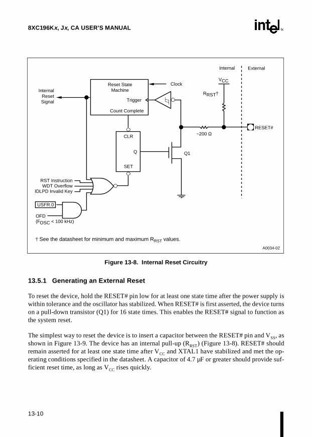
8XC196Kx, Jx, CA USER’S MANUAL
13-10
Figure 13-8. Internal Reset Circuitry
13.5.1 Generating an External Reset
To reset the device, hold the RESET# pin low for at least one state time after the power supply iswithin tolerance and the oscillator has stabilized. When RESET# is first asserted, the device turnson a pull-down transistor (Q1) for 16 state times. This enables the RESET# signal to function asthe system reset.
The simplest way to reset the device is to insert a capacitor between the RESET# pin and VSS, asshown in Figure 13-9. The device has an internal pull-up (RRST) (Figure 13-8). RESET# shouldremain asserted for at least one state time after VCC and XTAL1 have stabilized and met the op-erating conditions specified in the datasheet. A capacitor of 4.7 µF or greater should provide suf-ficient reset time, as long as VCC rises quickly.
A0034-02
Internal Reset Signal
Reset State Machine
Trigger
Clock
Internal External
RRST†
CLR
Q
RST Instruction WDT Overflow
IDLPD Invalid Key
RESET#~200 Ω
Count Complete
Q1
SET
VCC
USFR.0
OFD (FOSC < 100 kHz)
† See the datasheet for minimum and maximum RRST values.

13-11
MINIMUM HARDWARE CONSIDERATIONS
Figure 13-9. Minimum Reset Circuit
The other devices may not be reset because the capacitor will keep the voltage above VIL. SinceRESET# is asserted for only 16 state times, it may be necessary to lengthen and buffer the system-reset pulse. Figure 13-10 shows an example of a system-reset circuit. In this example, D2 createsa wired-OR gate connection to the reset pin. An internal reset, system power-up, or SW1 closingwill generate the system-reset signal.
Figure 13-10. Example System Reset Circuit
RESET#
8XC196 Device
+4.7 µF
A0276-01
RESET#
8XC196 Device
+4.7 µF
A0276-01
RESET#
8XC196 Device
System reset signal to external circuitry
(1)
Schmitt Triggers
Notes: 1. D1 provides a faster cycle time for repetitive power-on resets. 2. Optional pull-up for faster recovery.
R
C
4.7 kΩ
(2)D2
SW1
D1
A0277-02
VCCVCC

8XC196Kx, Jx, CA USER’S MANUAL
13-12
13.5.2 Issuing the Reset (RST) Instruction
The RST instruction (opcode FFH) resets the device by pulling RESET# low for 16 state times.It also clears the processor status word (PSW), sets the master program counter (PC) to 2080H,and resets the special function registers (SFRs). See Table C-2 on page C-2 for the reset valuesof the SFRs.
Putting pull-ups on the address/data bus causes unimplemented areas of memory to be read asFFH. If unused internal OTPROM memory is set to FFH, then execution from any unused mem-ory locations will reset the device.
13.5.3 Issuing an Illegal IDLPD Key Operand
The device resets itself if an illegal key operand is used with the idle/powerdown (IDLPD) com-mand. The legal keys are “1” for idle mode and “2” for powerdown mode. If any other value isused, the device executes a reset sequence. (See Appendix A for a description of the IDLPD com-mand.)
13.5.4 Enabling the Watchdog Timer
The watchdog timer (WDT) is a 16-bit counter that resets the device when the counter overflows(every 64K state times). The WDE bit (bit 3) of CCR1 controls whether the watchdog is enabledimmediately or is disabled until the first time it is cleared. Clearing WDE activates the watchdog.Setting WDE makes the watchdog timer inactive, but you can activate it by clearing the watchdogregister. Once the watchdog is activated, only a reset can disable it.
You must write two consecutive bytes to the watchdog register (location 0AH) to clear it. Thefirst byte must be 1EH and the second must be E1H. We recommend that you disable interruptsbefore writing to the watchdog register. If an interrupt occurs between the two writes, the watch-dog register will not be cleared.
If enabled, the watchdog continues to run in idle mode. The device must be awakened within 64Kstate times to clear the watchdog; otherwise, the watchdog will reset the device, which causes itto exit idle mode.
13.5.5 Detecting Oscillator Failure
The ability to sense an oscillator failure is important in safety-sensitive applications. This deviceprovides a feature that can detect a failed oscillator and reset itself. Low-frequency oscillation,typically 100 KHz or below, is sensed as a failure. If enabled, the oscillator fail detect (OFD) cir-cuitry resets the device in the event of an oscillator failure. This feature is enabled by program-ming the OFD bit (bit 0) in the USFR. (See “Enabling the Oscillator Failure Detection Circuitry”on page 16-8 for details.)

14Special Operating Modes

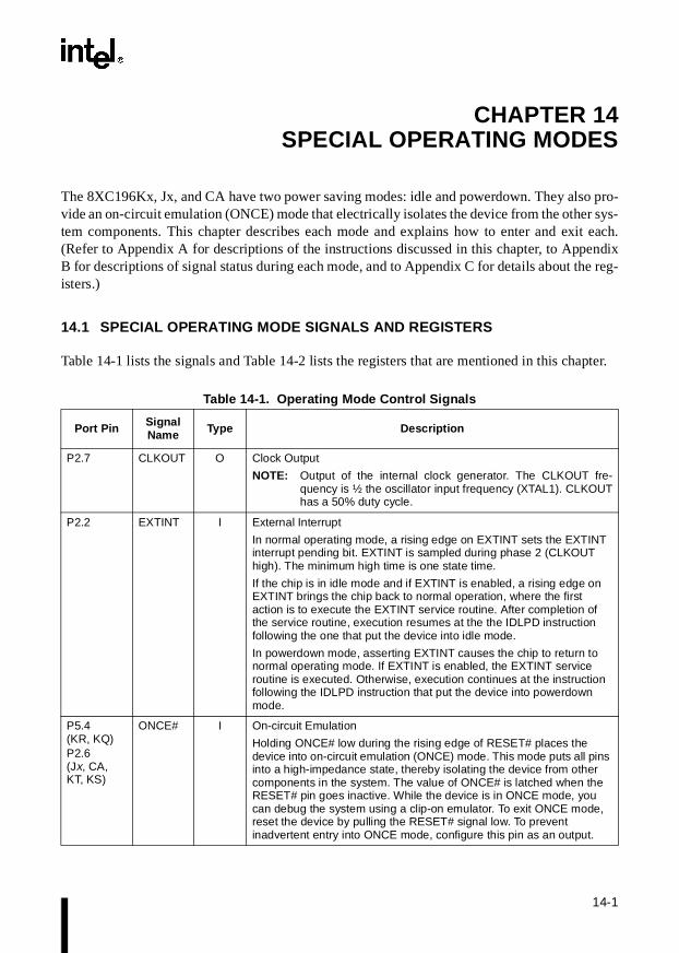
14-1
CHAPTER 14SPECIAL OPERATING MODES
The 8XC196Kx, Jx, and CA have two power saving modes: idle and powerdown. They also pro-vide an on-circuit emulation (ONCE) mode that electrically isolates the device from the other sys-tem components. This chapter describes each mode and explains how to enter and exit each.(Refer to Appendix A for descriptions of the instructions discussed in this chapter, to AppendixB for descriptions of signal status during each mode, and to Appendix C for details about the reg-isters.)
14.1 SPECIAL OPERATING MODE SIGNALS AND REGISTERS
Table 14-1 lists the signals and Table 14-2 lists the registers that are mentioned in this chapter.
Table 14-1. Operating Mode Control Signals
Port Pin SignalName Type Description
P2.7 CLKOUT O Clock Output
NOTE: Output of the internal clock generator. The CLKOUT fre-quency is ½ the oscillator input frequency (XTAL1). CLKOUThas a 50% duty cycle.
P2.2 EXTINT I External Interrupt
In normal operating mode, a rising edge on EXTINT sets the EXTINT interrupt pending bit. EXTINT is sampled during phase 2 (CLKOUT high). The minimum high time is one state time.
If the chip is in idle mode and if EXTINT is enabled, a rising edge on EXTINT brings the chip back to normal operation, where the first action is to execute the EXTINT service routine. After completion of the service routine, execution resumes at the the IDLPD instruction following the one that put the device into idle mode.
In powerdown mode, asserting EXTINT causes the chip to return to normal operating mode. If EXTINT is enabled, the EXTINT service routine is executed. Otherwise, execution continues at the instruction following the IDLPD instruction that put the device into powerdown mode.
P5.4(KR, KQ)P2.6(Jx, CA, KT, KS)
ONCE# I On-circuit Emulation
Holding ONCE# low during the rising edge of RESET# places the device into on-circuit emulation (ONCE) mode. This mode puts all pins into a high-impedance state, thereby isolating the device from other components in the system. The value of ONCE# is latched when the RESET# pin goes inactive. While the device is in ONCE mode, you can debug the system using a clip-on emulator. To exit ONCE mode, reset the device by pulling the RESET# signal low. To prevent inadvertent entry into ONCE mode, configure this pin as an output.
8XC196Kx, Jx, CA USER’S MANUAL
14-2
P5.4(CA, KT, KS)P2.6(KR, KQ)
Test-mode entry
I/O Test-mode entry
If this pin is held low during reset, the device will enter a reserved test mode, so exercise caution if you use this pin for input. If you choose to configure this pin as an input, always hold it high during reset and ensure that your system meets the VIH specification (see datasheet) to prevent inadvertent entry into a test mode.
— RESET# I/O Reset
A level-sensitive reset input to and open-drain system reset output from the microcontroller. Either a falling edge on RESET# or an internal reset turns on a pull-down transistor connected to the RESET pin for 16 state times. In the powerdown and idle modes, asserting RESET# causes the chip to reset and return to normal operating mode. The microcontroller resets to 2080H.
— VPP PWR Programming Voltage
During programming, the VPP pin is typically at +12.5 V (VPP voltage). Exceeding the maximum VPP voltage specification can damage the device.
VPP also causes the device to exit powerdown mode when it is driven low for at least 50 ns. Use this method to exit powerdown only when using an external clock source because it enables the internal phase clocks, but not the internal oscillator.
On devices with no internal nonvolatile memory, connect VPP to VCC.
Table 14-2. Operating Mode Control and Status Registers
Mnemonic Address Description
CCR0 2018H Chip Configuration 0 Register
Bit 0 of this register enables and disables powerdown mode.
INT_MASK1 0013H Interrupt Mask 1
Bit 6 of this 8-bit register enables and disables (masks) the external interrupt (EXTINT).
INT_PEND1 0012H Interrupt Pending 1
When set, bit 6 of this register indicates a pending external interrupt.
P2_DIRP5_DIR
1FCBH 1FF3H
Port x Direction
Each bit of Px_DIR controls the direction of the corresponding pin. Clearing a bit configures a pin as a complementary output; setting a bit configures a pin as an input or open-drain output. (Open-drain outputs require external pull-ups.)
P2_MODEP5_MODE
1FC9H1FF1H
Port x Mode
Each bit of Px_MODE controls whether the corresponding pin functions as a standard I/O port pin or as a special-function signal. Setting a bit configures a pin as a special-function signal; clearing a bit configures a pin as a standard I/O port pin.
Table 14-1. Operating Mode Control Signals (Continued)
Port Pin SignalName Type Description

14-3
SPECIAL OPERATING MODES
14.2 REDUCING POWER CONSUMPTION
Both power-saving modes conserve power by disabling portions of the internal clock circuitry(Figure 14-1). The following paragraphs describe both modes in detail.
Figure 14-1. Clock Control During Power-saving Modes
14.3 IDLE MODE
In idle mode, the device’s power consumption decreases to approximately 40% of normal con-sumption. Internal logic holds the CPU clocks at logic zero, causing the CPU to stop executinginstructions. Neither the peripheral clocks nor CLKOUT are affected, so the special-function reg-isters (SFRs) and register RAM retain their data and the peripherals and interrupt system remainactive. Tables in Appendix B list the values of the pins during idle mode (see Table B-8 on pageB-20 for the 8XC196Kx, Table B-9 on page B-21 for the 8XC196Jx, or Table B-10 on page B-22for the 87C196CA).
A3064-02
Clock Generators
CPU Clocks (PH1, PH2)
Divide-by-two Circuit
Peripheral Clocks (PH1, PH2)
CLKOUT
Disable Clocks (Powerdown)
Disable Clocks (Idle, Powerdown)
XTAL1
XTAL2
FOSC
Disable Oscillator
(Powerdown)
Disable Clock Input (Powerdown)

8XC196Kx, Jx, CA USER’S MANUAL
14-4
The device enters idle mode after executing the IDLPD #1 instruction. Either an interrupt or ahardware reset will cause the device to exit idle mode. Any enabled interrupt source, either inter-nal or external, can cause the device to exit idle mode. When an interrupt occurs, the CPU clocksrestart and the CPU executes the corresponding interrupt service or PTS routine. When the routineis complete, the CPU fetches and then executes the instruction that follows the IDLPD #1 instruc-tion.
NOTE
If enabled, the watchdog timer continues to run in idle mode. The device must be awakened within every 64K state times to clear the WATCHDOG register; otherwise, the timer will reset the device.
To prevent an accidental return to full power, hold the external interrupt pin (EXTINT) low while the device is in idle mode.
14.4 POWERDOWN MODE
Powerdown mode places the device into a very low power state by disabling the internal oscillatorand clock generators. Internal logic holds the CPU and peripheral clocks at logic zero, whichcauses the CPU to stop executing instructions, the system bus-control signals to become inactive,the CLKOUT signal to become high, and the peripherals to turn off. Power consumption dropsinto the microwatt range (refer to the datasheet for exact specifications). ICC is reduced to deviceleakage. Tables in Appendix B list the values of the pins during powerdown mode (see Table B-8on page B-20 for the 8XC196Kx, Table B-9 on page B-21 for the 8XC196Jx, or Table B-10 onpage B-22 for the 87C196CA). If VCC is maintained above the minimum specification, the spe-cial-function registers (SFRs) and register RAM retain their data.
14.4.1 Enabling and Disabling Powerdown Mode
Setting the PD bit in the chip-configuration register 0 (CCR0.0) enables powerdown mode. Clear-ing it disables powerdown. CCR0 is loaded from the chip configuration byte (CCB0) when thedevice is reset.
14-5
SPECIAL OPERATING MODES
14.4.2 Entering Powerdown Mode
Before entering powerdown, complete the following tasks:
• Complete all serial port transmissions or receptions. Otherwise, when the device exitspowerdown, the serial port activity will continue where it left off and incorrect data may betransmitted or received.
• Complete all analog conversions. If powerdown occurs during the conversion, the resultwill be incorrect.
• If the watchdog timer (WDT) is enabled, clear the WATCHDOG register just before issuingthe powerdown instruction. This ensures that the device can exit powerdown cleanly.Otherwise, the WDT could reset the device before the oscillator stabilizes. (The WDTcannot reset the device during powerdown because the clock is stopped.)
• Put all other peripherals into an inactive state.
• 8XC196Kx: To allow other devices to control the bus while the microcontroller is inpowerdown, assert HLDA#. Do this only if the routines for entering and exiting powerdowndo not require access to external memory.
After completing these tasks, execute the IDLPD #2 instruction to enter powerdown mode.
NOTE
To prevent an accidental return to full power, hold the external interrupt pin (EXTINT) low while the device is in powerdown mode.
14.4.3 Exiting Powerdown Mode
The device will exit powerdown mode when one of the following events occurs:
• an external device drives the VPP pin low for at least 50 ns,
• a hardware reset is generated,
• or a transition occurs on the external interrupt pin.
14.4.3.1 Driving the V PP Pin Low
If the design uses an external clock input signal rather than the on-chip oscillator, the fastest wayto exit powerdown mode is to drive the VPP pin low for at least 50 ns. Use this method only whenusing an external clock input because the internal CPU and peripheral clocks will be enabled, butnot the internal oscillator.
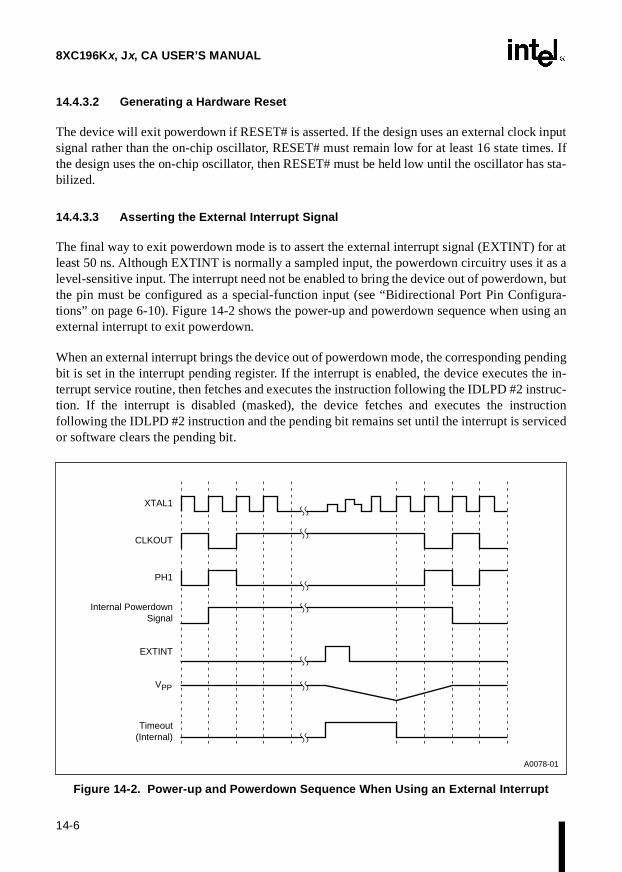
8XC196Kx, Jx, CA USER’S MANUAL
14-6
14.4.3.2 Generating a Hardware Reset
The device will exit powerdown if RESET# is asserted. If the design uses an external clock inputsignal rather than the on-chip oscillator, RESET# must remain low for at least 16 state times. Ifthe design uses the on-chip oscillator, then RESET# must be held low until the oscillator has sta-bilized.
14.4.3.3 Asserting the External Interrupt Signal
The final way to exit powerdown mode is to assert the external interrupt signal (EXTINT) for atleast 50 ns. Although EXTINT is normally a sampled input, the powerdown circuitry uses it as alevel-sensitive input. The interrupt need not be enabled to bring the device out of powerdown, butthe pin must be configured as a special-function input (see “Bidirectional Port Pin Configura-tions” on page 6-10). Figure 14-2 shows the power-up and powerdown sequence when using anexternal interrupt to exit powerdown.
When an external interrupt brings the device out of powerdown mode, the corresponding pendingbit is set in the interrupt pending register. If the interrupt is enabled, the device executes the in-terrupt service routine, then fetches and executes the instruction following the IDLPD #2 instruc-tion. If the interrupt is disabled (masked), the device fetches and executes the instructionfollowing the IDLPD #2 instruction and the pending bit remains set until the interrupt is servicedor software clears the pending bit.
Figure 14-2. Power-up and Powerdown Sequence When Using an External Interrupt
XTAL1
CLKOUT
PH1
Internal Powerdown Signal
EXTINT
VPP
Timeout (Internal)
A0078-01

14-7
SPECIAL OPERATING MODES
When using an external interrupt signal to exit powerdown mode, we recommend that you con-nect the external RC circuit shown in Figure 14-3 to the VPP pin. The discharging of the capacitorcauses a delay that allows the oscillator to stabilize before the internal CPU and peripheral clocksare enabled.
Figure 14-3. External RC Circuit
During normal operation (before entering powerdown mode), an internal pull-up holds theVPP pin at VCC. When an external interrupt signal is asserted, the internal oscillator circuitry isenabled and turns on a weak internal pull-down. This weak pull-down causes the external capac-itor (C1) to begin discharging at a typical rate of 200 µA. When the VPP pin voltage drops belowthe threshold voltage (about 2.5 V), the internal phase clocks are enabled and the device resumescode execution.
At this time, the internal pull-up transistor turns on and quickly pulls the pin back up to about3.5 V. The pull-up becomes ineffective and the external resistor (R1) takes over and pulls the volt-age up to VCC (see recovery time in Figure 14-4). The time constant follows an exponential charg-ing curve. If C1 = 1 µF and R1 = 1 MΩ, the recovery time will be one second.
14.4.3.4 Selecting R 1 and C 1
The values of R1 and C1 are not critical. Select components that produce a sufficient dischargetime to permit the internal oscillator circuitry to stabilize. Because many factors can influence thedischarge time requirement, you should always fully characterize your design under worst-caseconditions to verify proper operation.
8XC196 Device
R1 1 MΩ Typical
C1 1µF Typical
VPP
A0279-01
VCC

8XC196Kx, Jx, CA USER’S MANUAL
14-8
Figure 14-4. Typical Voltage on the V PP Pin While Exiting Powerdown
Select a resistor that will not interfere with the discharge current. In most cases, values between200 kΩ and 1 MΩ should perform satisfactorily. When selecting the capacitor, determine theworst-case discharge time needed for the oscillator to stabilize, then use this formula to calculatean appropriate value for C1.
where:
C1 is the capacitor value, in farads
TDIS is the worst-case discharge time, in seconds
I is the discharge current, in amperes
Vt is the threshold voltage
NOTE
If powerdown is re-entered and exited before C1 charges to VCC, it will take less time for the voltage to ramp down to the threshold. Therefore, the device will take less time to exit powerdown.
VPP, Volts
1
2
3
4
5
200 µA C1 Discharge
Pullup On Code Execution Resumes
R1 x C1 RecoveryTime Constant
EXTINT
Time, ms2 4 6 8 10 12 14 16 18 20 22
A0151-01
C1
TDIS I×Vt
--------------------=
14-9
SPECIAL OPERATING MODES
For example, assume that the oscillator needs at least 12.5 ms to discharge (TDIS = 12.5 ms), Vtis 2.5 V, and the discharge current is 200 µA. The minimum C1 capacitor size is 1 µF.
When using an external oscillator, the value of C1 can be very small, allowing rapid recovery frompowerdown. For example, a 100 pF capacitor discharges in 1.25 µs.
14.5 ONCE MODE
On-circuit emulation (ONCE) mode isolates the device from other components in the system toallow printed-circuit-board testing or debugging with a clip-on emulator. During ONCE mode,all pins except XTAL1, XTAL2, VSS, and VCC are weakly pulled high or low. During ONCEmode, RESET# must be held high or the device will exit ONCE mode and enter the reset state.Tables in Appendix B list the reset states of the pins (see Table B-8 on page B-20 for the8XC196Kx, Table B-9 on page B-21 for the 8XC196Jx, or Table B-10 on page B-22 for the87C196CA).
14.5.1 Entering and Exiting ONCE Mode
Holding the ONCE# signal low during the rising edge of RESET# causes the device to enterONCE mode. To prevent accidental entry into ONCE mode, we highly recommend configuringthis pin as an output. If you choose to configure this pin as an input, always hold it high duringreset and ensure that your system meets the VIH specification (see datasheet) to prevent inadvert-ent entry into ONCE mode. Table 14-3 shows the ONCE# pin multiplexing for each device in the8XC196Kx, Jx, and CA product families.
Exit ONCE mode by asserting the RESET# signal and allowing the ONCE# pin to float or bepulled high. Normal operations resume when RESET# goes high.
Table 14-3. ONCE# Pin Alternate Functions
Device ONCE# Alternate Functions
8XC196CA P2.6/HLDA#
8XC196Jx P2.6/HLDA#
8XC196KQ, KR P5.4/SLPINT
8XC196KS, KT P2.6/HLDA#
C10.0125 0.0002×
2.5------------------------------------------- 1 µF= =
TDIS
C1 Vt×
I------------------
1.0 1010–× 2.5×
0.0002------------------------------------------- 1.25 µs= = =

8XC196Kx, Jx, CA USER’S MANUAL
14-10
14.6 RESERVED TEST MODES
A special test-mode-entry pin (Table 14-4) is provided for Intel’s in-house testing only. These testmodes can be entered accidentally if you configure the test-mode-entry pin as an input and holdit low during the rising edge of RESET#. To prevent accidental entry into an unsupported testmode, we highly recommend configuring the test-mode-entry pin as an output. If you choose toconfigure this pin as an input, always hold it high during reset and ensure that your system meetstheVIH specification (see datasheet) to prevent inadvertent entry into an unsupported test mode.
Table 14-4. Test-mode-entry Pins
Device Test-Mode-Entry Pin
8XC196CA P5.4
8XC196Jx Not implemented
8XC196KQ, KR P2.6
8XC196KS, KT P5.4

15Interfacing with External Memory


15-1
CHAPTER 15INTERFACING WITH EXTERNAL MEMORY
The device can interface with a variety of external memory devices. It supports either a fixed 8-bit bus width, a fixed 16-bit bus width, or a dynamic 8-bit/16-bit bus width; internal control ofwait states for slow external memory devices; a bus-hold protocol that enables external devicesto take over the bus; and several bus-control modes. These features provide a great deal of flexi-bility when interfacing with external memory devices.
In addition to describing the signals and registers related to external memory, this chapter discuss-es the process of fetching the chip configuration bytes and configuring the external bus. It alsoprovides examples of external memory configurations.
15.1 EXTERNAL MEMORY INTERFACE SIGNALS
Table 15-1 describes the external memory interface signals. For some signals, the pin has an al-ternate function (shown in the Multiplexed With column). In some cases the alternate function isa port signal (e.g., P2.7). Chapter 6, “I/O Ports,” describes how to configure a pin for its I/O portfunction and for its special function. In other cases, the signal description includes instructionsfor selecting the alternate function.
Table 15-1. External Memory Interface Signals
FunctionName Type Description Multiplexed
With
AD15:0 I/O Address/Data Lines
These pins provide a multiplexed address and data bus. During the address phase of the bus cycle, address bits 0–15 are presented on the bus and can be latched using ALE or ADV#. During the data phase, 8- or 16-bit data is transferred. When a bus access is not occurring, these pins revert to their I/O port function.
P4.7:0
P3.7:0
ADV# O Address Valid
This active-low output signal is asserted only during external memory accesses. ADV# indicates that valid address information is available on the system address/data bus. The signal remains low while a valid bus cycle is in progress and is returned high as soon as the bus cycle completes.
An external latch can use this signal to demultiplex the address from the address/data bus. A decoder can also use this signal to generate chip selects for external memory.
ALE/P5.0

8XC196Kx, Jx, CA USER’S MANUAL
15-2
ALE O Address Latch Enable
This active-high output signal is asserted only during external memory cycles. ALE signals the start of an external bus cycle and indicates that valid address information is available on the system address/data bus. ALE differs from ADV# in that it does not remain active during the entire bus cycle.
An external latch can use this signal to demultiplex the address from the address/data bus.
ADV#/P5.0
BHE#† O Byte High Enable
The chip configuration register 0 (CCR0) determines whether this pin functions as BHE# or WRH#. CCR0.2=1 selects BHE#; CCR0.2=0 selects WRH#.
During 16-bit bus cycles, this active-low output signal is asserted for word reads and writes and high-byte reads and writes to external memory. BHE# indicates that valid data is being transferred over the upper half of the system data bus. BHE#, in conjunction with AD0, indicates the memory byte that is being transferred over the system bus:
BHE# AD0 Byte(s) Accessed
0 0 both bytes0 1 high byte only1 0 low byte only† This pin is not implemented on the 8XC196Jx device.
P5.5/WRH#
BREQ#† O Bus Request
This active-low output signal is asserted during a hold cycle when the bus controller has a pending external memory cycle.
The device can assert BREQ# at the same time as or after it asserts HLDA#. Once it is asserted, BREQ# remains asserted until HOLD# is removed.
You must enable the bus-hold protocol before using this signal (see “Enabling the Bus-hold Protocol (8XC196Kx Only)” on page 15-18).† This pin is not implemented on the 87C196CA, 8XC196Jx devices.
P2.3
BUSWIDTH† I Bus Width
The chip configuration register bits, CCR0.1 and CCR1.2, along with the BUSWIDTH pin, control the data bus width. When both CCR bits are set, the BUSWIDTH signal selects the external data bus width. When only one CCR bit is set, the bus width is fixed at either 16 or 8 bits, and the BUSWIDTH signal has no effect.
CCR0.1 CCR1.2 BUSWIDTH0 1 N/A fixed 8-bit data bus1 0 N/A fixed 16-bit data bus1 1 high 16-bit data bus1 1 low 8-bit data bus† This pin is not implemented on the 87C196CA, 8XC196Jx devices.
P5.7
Table 15-1. External Memory Interface Signals (Continued)
FunctionName Type Description Multiplexed
With

15-3
INTERFACING WITH EXTERNAL MEMORY
CLKOUT O Clock Output
Output of the internal clock generator. The CLKOUT frequency is ½ the oscillator frequency input (XTAL1). CLKOUT has a 50% duty cycle.
P2.7
EA# I External Access
EA# is sampled and latched only on the rising edge of RESET#. Changing the level of EA# after reset has no effect. Accesses to special-purpose and program memory partitions are directed to internal memory if EA# is held high and to external memory if EA# is held low. (See Table 4-1 on page 4-2 for address ranges of special-purpose and program memory partitions.)
EA# also controls program mode entry. If EA# is at VPP voltage (typically +12.5 V) on the rising edge of RESET#, the device enters programming mode.
NOTE: When EA# is active, ports 3 and 4 will function only as theaddress/data bus. They cannot be used for standard I/O.
On devices with no internal nonvolatile memory, always connect EA# to VSS.
—
HLDA#† O Bus Hold Acknowledge
This active-low output indicates that the CPU has released the bus as the result of an external device asserting HOLD#.† The P2.6 pin does not function as HLDA# on the 87C196CA, 8XC196Jx devices.
P2.6
HOLD#† I Bus Hold Request
An external device uses this active-low input signal to request control of the bus. This pin functions as HOLD# only if the pin is configured for its special function (see “Bidirectional Port Pin Configurations” on page 6-10) and the bus-hold protocol is enabled. Setting bit 7 of the window selection register enables the bus-hold protocol.† This pin is not implemented on the 87C196CA, 8XC196Jx devices.
P2.5
INTOUT#† O Interrupt Output
This active-low output indicates that a pending interrupt requires use of the external bus.† This pin is not implemented on the 87C196CA, 8XC196Jx devices.
AINC#/P2.4
INST† O Instruction Fetch
This active-high output signal is valid only during external memory bus cycles. When high, INST indicates that an instruction is being fetched from external memory. The signal remains high during the entire bus cycle of an external instruction fetch. INST is low for data accesses, including interrupt vector fetches and chip configuration byte reads. INST is low during internal memory fetches.† This pin is not implemented on the 87C196CA, 8XC196Jx devices.
P5.1
RD# O Read
Read-signal output to external memory. RD# is asserted only during external memory reads.
P5.3
Table 15-1. External Memory Interface Signals (Continued)
FunctionName Type Description Multiplexed
With

8XC196Kx, Jx, CA USER’S MANUAL
15-4
15.2 CHIP CONFIGURATION REGISTERS AND CHIP CONFIGURATION BYTES
Two chip configuration registers (CCRs) have bits that set parameters for chip operation and ex-ternal bus cycles. The CCRs cannot be accessed by code. They are loaded from the chip config-uration bytes (CCBs), which have addresses 2018H (CCB0) and 201AH (CCB1).
When the device returns from reset, the bus controller fetches the CCBs and loads them into theCCRs. From this point, these CCR bit values define the chip configuration until the device is resetagain. The CCR bits are described in Figures 15-1 and 15-2.
READY† I Ready Input
This active-high input signal is used to lengthen external memory cycles for slow memory by generating wait states in addition to the wait states that are generated internally.
When READY is high, CPU operation continues in a normal manner with wait states inserted as programmed in the chip configuration registers. READY is ignored for all internal memory accesses.† This pin is not implemented on the 8XC196Jx device.
P5.6
WR# O Write
The chip configuration register 0 (CCR0) determines whether this pin functions as WR# or WRL#. CCR0.2=1 selects WR#; CCR0.2=0 selects WRL#.
This active-low output indicates that an external write is occurring. This signal is asserted only during external memory writes.
P5.2/WRL#
WRH#† O Write High
The chip configuration register 0 (CCR0) determines whether this pin functions as BHE# or WRH#. CCR0.2=1 selects BHE; CCR0.2=0 selects WRH#.
During 16-bit bus cycles, this active-low output signal is asserted for high-byte writes and word writes to external memory. During 8-bit bus cycles, WRH# is asserted for all write operations.† This pin is not implemented on the 87C196CA, 8XC196Jx devices.
P5.5/BHE#
WRL# O Write Low
The chip configuration register 0 (CCR0) determines whether this pin functions as WR# or WRL#. CCR0.2=1 selects WR#; CCR0.2=0 selects WRL#.
During 16-bit bus cycles, this active-low output signal is asserted for low-byte writes and word writes. During 8-bit bus cycles, WRL# is asserted for all write operations.
P5.2/WR#
Table 15-1. External Memory Interface Signals (Continued)
FunctionName Type Description Multiplexed
With

15-5
INTERFACING WITH EXTERNAL MEMORY
CCR0 Address:Reset State:
2018HXXH
The chip configuration 0 (CCR0) register controls powerdown mode, bus-control signals, and internal memory protection. Three of its bits combine with two bits of CCR1 to control wait states and bus width.
7 0
LOC1 LOC0 IRC1 IRC0 ALE WR BW0 PD
Bit Number
Bit Mnemonic Function
7:6 LOC1:0 Lock Bits
Determine the programming protection scheme for internal memory.
LOC1 LOC0
0 0 read and write protect0 1 read protect only1 0 write protect only1 1 no protection
5:4 IRC1:0 Internal Ready Control
These two bits, along with IRC2 (CCR1.1), limit the number of wait states that can be inserted while the READY pin is held low. Wait states are inserted into the bus cycle either until the READY pin is pulled high or until this internal number is reached.
IRC2 IRC1 IRC0
0 0 0 zero wait states0 X 1 illegal0 1 X illegal1 0 0 one wait state1 0 1 two wait states1 1 0 three wait states1 1 1 infinite†
† This mode is unavailable on the 8XC196Jx device. On this device, the READY pin is not implemented. Therefore, the number of wait states inserted into the bus cycle is determined only by the IRC2:0 bit settings.
Figure 15-1. Chip Configuration 0 (CCR0) Register

8XC196Kx, Jx, CA USER’S MANUAL
15-6
3 ALE Address Valid Strobe and Write Strobe
These bits define which bus-control signals will be generated during external read and write cycles.
ALE WR
0 0 address valid with write strobe mode(ADV#, RD#, WRL#, WRH#)†
0 1 address valid strobe mode(ADV#, RD#, WR#, BHE#)†
1 0 write strobe mode(ALE, RD#, WRL#, WRH#)†
1 1 standard bus-control mode(ALE, RD#, WR#, BHE#)†
† On the 8XC196Jx device, the BHE#/WRH# pin is not implemented.
2 WR
1 BW0 Buswidth Control
This bit, along with the BW1 bit (CCR1.2), selects the bus width.
BW1 BW0
0 0 illegal0 1 16-bit only1 0 8-bit only1 1 BUSWIDTH pin controlled†
† This mode is unavailable on the 87C196CA, 8XC196Jx devices. The BUSWIDTH pin is not implemented.
0 PD Powerdown Enable
Controls whether the IDLPD #2 instruction causes the device to enter powerdown mode. Clearing this bit at reset can prevent accidental entry into powerdown mode.
1 = enable powerdown mode0 = disable powerdown mode
CCR0 (Continued) Address:Reset State:
2018HXXH
The chip configuration 0 (CCR0) register controls powerdown mode, bus-control signals, and internal memory protection. Three of its bits combine with two bits of CCR1 to control wait states and bus width.
7 0
LOC1 LOC0 IRC1 IRC0 ALE WR BW0 PD
Bit Number
Bit Mnemonic Function
Figure 15-1. Chip Configuration 0 (CCR0) Register (Continued)

15-7
INTERFACING WITH EXTERNAL MEMORY
CCR1 Address:Reset State:
201AHXXH
The chip configuration 1 (CCR1) register enables the watchdog timer and selects the bus timing mode. Two of its bits combine with three bits of CCR0 to control wait states and bus width.
7 0
CA, Jx, KQ, KR 1 1 0 1 WDE BW1 IRC2 0
7 0
KS, KT MSEL1 MSEL0 0 1 WDE BW1 IRC2 0
BitNumber
BitMnemonic Function
7:6 1(CA, Jx, KQ, KR)
To guarantee device operation, write ones to these bits.
MSEL1:0(KS, KT)
External Access Timing Mode Select
These bits control the bus-timing modes.
MSEL1 MSEL00 0 standard mode plus one wait state0 1 long read/write1 0 long read/write with early address1 1 standard mode
5 0 To guarantee device operation, write zero to this bit.
4 1 To guarantee device operation, write one to this bit.
3 WDE Watchdog Timer Enable
Selects whether the watchdog timer is always enabled or enabled the first time it is cleared.
1 = enabled first time it is cleared0 = always enabled
2 BW1 Buswidth Control
This bit, along with the BW0 bit (CCR0.1), selects the bus width.
BW1 BW00 0 illegal0 1 16-bit only1 0 8-bit only1 1 BUSWIDTH pin controlled†
† This mode is unavailable on the 87C196CA, 8XC196Jx devices. The BUSWIDTH pin is not implemented.
Figure 15-2. Chip Configuration 1 (CCR1) Register

8XC196Kx, Jx, CA USER’S MANUAL
15-8
15.3 BUS WIDTH AND MULTIPLEXING
The external bus can operate as either a 16-bit multiplexed address/data bus or as a multiplexed16-bit address/8-bit data bus (Figure 15-3).
1 IRC2 Ready Control
This bit, along with IRC0 (CCR0.4) and IRC1 (CCR0.5), limits the number of wait states that can be inserted while the READY pin is held low. Wait states are inserted into the bus cycle either until the READY pin is pulled high or until this internal number is reached.
IRC2 IRC1 IRC00 0 0 zero wait states0 X 1 illegal0 1 X illegal1 0 0 one wait state1 0 1 two wait states1 1 0 three wait states1 1 1 infinite†
† This mode is unavailable on the 8XC196Jx device. On this device, the READY pin is not implemented. Therefore, the number of wait states inserted into the bus cycle is determined only by the IRC2:0 bit settings.
0 — Reserved; always write as zero.
CCR1 (Cont inued) Address:Reset State:
201AHXXH
The chip configuration 1 (CCR1) register enables the watchdog timer and selects the bus timing mode. Two of its bits combine with three bits of CCR0 to control wait states and bus width.
7 0
CA, Jx, KQ, KR 1 1 0 1 WDE BW1 IRC2 0
7 0
KS, KT MSEL1 MSEL0 0 1 WDE BW1 IRC2 0
BitNumber
BitMnemonic Function
Figure 15-2. Chip Configuration 1 (CCR1) Register (Continued)

15-9
INTERFACING WITH EXTERNAL MEMORY
Figure 15-3. Multiplexing and Bus Width Options
After reset, but before the CCB fetch, the device is configured for 8-bit bus mode, regardless ofthe BUSWIDTH input. The upper address lines (AD15:8) are weakly driven throughout theCCB0 and CCB1 bus cycles. To prevent bus contention, neither pull-ups nor pull-downs shouldbe used on AD15:8. Also, the upper bytes of the CCB words (locations 2019H and 201BH)should be loaded with 20H. If the external memory outputs 20H on its high byte, there will be nobus contention.
After the CCBs are loaded into the CCRs, the values of BW0 and BW1 define the data bus widthas either a fixed 8-bit, a fixed 16-bit, or a dynamic 16-bit/8-bit bus width controlled by theBUSWIDTH signal (The BW0 and BW1 bits are defined in Figures 15-1 and 15-2).
If BW0 is clear and BW1 is set, the bus controller is locked into an 8-bit bus mode. In comparingan 8-bit bus system to a 16-bit bus system, expect some performance degradation. In a 16-bit bussystem, a word fetch is done with a single word fetch. However, in an 8-bit bus system, a wordfetch takes an additional bus cycle because it must be done with two byte fetches.
If BW0 is set and BW1 is clear, the bus controller is locked into a 16-bit bus mode. If both BW0and BW1 are set, the BUSWIDTH signal controls the bus width. The bus is 16 bits wide whenBUSWIDTH is high and 8 bits wide when BUSWIDTH is low. The BUSWIDTH signal is sam-pled after the address is on the bus, as shown in Figure 15-4.
Bus Control
16-bit Multiplexed Address/Data
AD15:0 (Ports 4 and 3)
8XC196
Bus Control
AD15:8 (Port 4)
8XC196
8-bit Multiplexed Address/Data
8-bit Address High
AD7:0 (Port 3)
8-bit Bus16-bit BusA3068-01

8XC196Kx, Jx, CA USER’S MANUAL
15-10
Figure 15-4. BUSWI DTH Timing Diagram
The BUSWIDTH signal can be used in numerous applications. For example, a system could storecode in a 16-bit memory device and data in an 8-bit memory device. The BUSWIDTH signalcould be tied to the chip-select input of the 8-bit memory device (shown in Figure 15-12 on page15-23). When BUSWIDTH is low, it enables 8-bit bus mode and selects the 8-bit memory device.When BUSWIDTH is high, it enables 16-bit bus mode and deselects the 8-bit memory device.
15.3.1 Timing Requirements for BUSWIDTH
When using BUSWIDTH to dynamically change between 8-bit and 16-bit bus widths, setup andhold timings must be met for proper operation (see Figure 15-4). Because a decoded, valid ad-dress is used to generate the BUSWIDTH signal, the setup time is specified relative to the addressbeing valid. This specification, TAVGV, indicates how much time one has to decode the valid ad-dress and generate a valid BUSWIDTH signal.
BUSWIDTH must be held valid until the minimum hold specification, TCLGX, has been met. Typ-ically this hold time is 0 ns minimum after CLKOUT goes low. In all cases, refer to the data sheetfor current specifications for TAVGV and TCLGX.
NOTE
Earlier HMOS devices used a BUSWIDTH setup timing that was referenced to the falling edge of ALE (TLLGV). This specification is not meaningful for CMOS devices, which use an internal two-phase clock; it is included for comparison only.
TLLGV
Bus
XTAL1
BUSWIDTH
ALE
CLKOUT
TAVGV
TCLGX (MIN)
Valid
A0164-02
Address Data

15-11
INTERFACING WITH EXTERNAL MEMORY
15.3.2 16-bit Bus Timings
When the device is configured to operate in the 16-bit bus-width mode, lines AD15:0 form a 16-bit multiplexed address/data bus. Figure 15-5 shows an idealized timing diagram for the externalread and write cycles. (Comprehensive timing specifications are shown in Figure 15-24).
The rising edge of the address latch enable (ALE) indicates that the device is driving an addressonto the bus (AD15:0). The device presents a valid address before ALE falls. The ALE signal isused to strobe a transparent latch (such as a 74AC373), which captures the address from AD15:0and holds it while the bus controller puts data onto AD15:0.
For 16-bit read cycles, the bus controller floats the bus and then drives RD# low so that it canreceive data. The external memory must put data (Data In) onto the bus before the rising edge ofRD#. The data sheet specifies the maximum time the memory device has to output valid data afterRD# is asserted. When INST is asserted, it indicates that the read operation is an instruction fetch.
For 16-bit write cycles, the bus controller drives WR# low, then puts data onto the bus. The risingedge of WR# signifies that data is valid. At this time, the external system must latch the data.
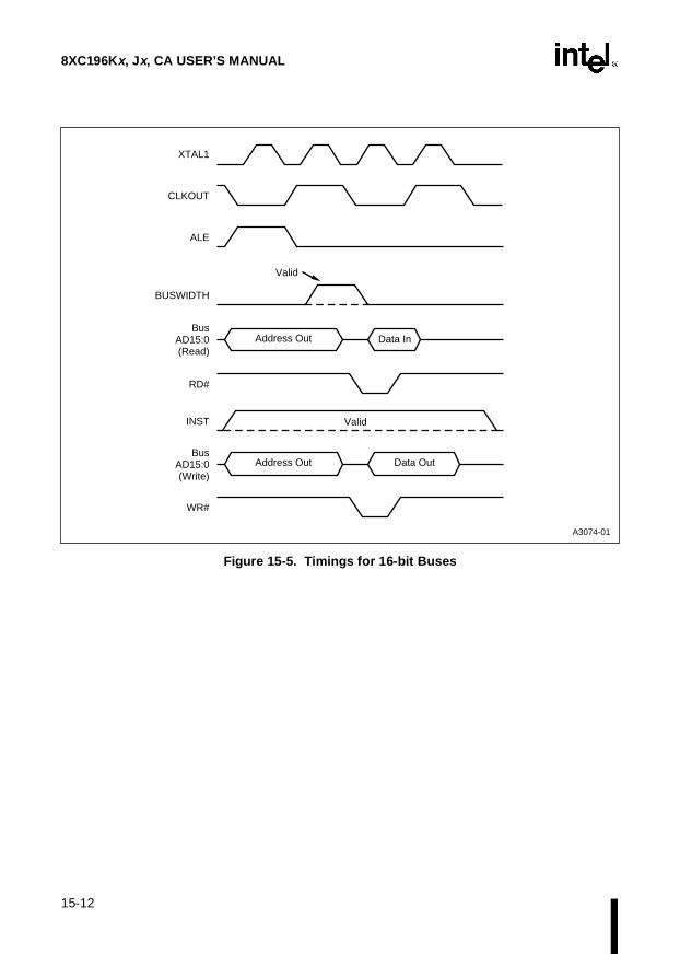
8XC196Kx, Jx, CA USER’S MANUAL
15-12
Figure 15-5. Timings for 16-bit Buses
XTAL1
CLKOUT
ALE
BUSWIDTH
Bus AD15:0 (Read)
RD#
INST
Bus AD15:0 (Write)
WR#
Address Out
Data Out
Data In
Address Out
Valid
Valid
A3074-01

15-13
INTERFACING WITH EXTERNAL MEMORY
15.3.3 8-bit Bus Timings
When the device is configured to operate in the 8-bit bus mode, lines AD7:0 form a multiplexedlower address and data bus. Lines AD15:8 are not multiplexed; the upper address is latched andremains valid throughout the bus cycle. Figure 15-6 shows an idealized timing diagram for theexternal read and write cycles. One cycle is required for an 8-bit read or write. A 16-bit accessrequires two cycles. The first cycle accesses the lower byte, and the second cycle accesses theupper byte. Except for requiring an extra cycle to write the bytes separately, the timings are thesame as on the 16-bit bus.
The ALE signal is used to demultiplex the lower address by strobing a transparent latch (such asa 74AC373).
For 8-bit bus read cycles, after ALE falls, the bus controller floats the bus and drives the RD#signal low. The external memory then must put its data on the bus. That data must be valid at therising edge of the RD# signal. To read a data word, the bus controller performs two consecutivereads, reading the low byte first, followed by the high byte.
For 8-bit bus write cycles, after ALE falls, the bus controller outputs data on AD7:0 and thendrives WR# low. The external memory must latch the data by the time WR# goes high. That datawill be valid on the bus until slightly after WR# goes high. To write a data word, the bus controllerperforms two consecutive writes, writing the low byte first, followed by the high byte.

8XC196Kx, Jx, CA USER’S MANUAL
15-14
Figure 15-6. Timings for 8-bit Buses
15.4 WAIT STATES (READY CONTROL)
An external device can use the READY input to request wait states in addition to the wait statesthat are generated internally by the 87C196CA, 8XC196Jx, Kx device. When an address is placedon the bus for an external bus cycle, the external device can pull the READY signal low to indi-cate it is not ready. In response, the bus controller inserts wait states to lengthen the bus cycle untilthe external device raises the READY signal. Each wait state adds one CLKOUT period (i.e., onestate time or 2TOSC) to the bus cycle.
CLKOUT
ALE
BUSWIDTH
Bus AD15:8
RD#
INST
Bus AD7:0 (Write)
WR#
Address Out
Address Out
Low data in
Address Out Low data out
Bus AD7:0 (Read)
XTAL1
Address +1 Out
High data out
High data in
Address Out
Address +1 Out
A3075-01
15-15
INTERFACING WITH EXTERNAL MEMORY
After reset and until CCB1 is read, the bus controller always inserts three wait states into bus cy-cles. Then, until P5.6 has been configured to operate as the READY signal, the internal readycontrol bits (IRC2:0) control the wait states. If IRC2:0 are all set during CCB0 and CCB1 fetch,READY (P5.6) is configured as a special-function input. If port 5 is initialized after reset, youmust ensure that P5.6 remains configured as the READY input. If P5.6 is configured as a portpin, the READY input to the device is equal to zero. This will cause an infinite number of waitstates to be inserted into bus cycles and the chip to lock up.
After the CCB1 fetch, the internal ready control circuitry allows slow external memory devicesto increase the length of the read and write bus cycles. If the external memory device is not readyfor access, it pulls the READY signal low and holds it low until it is ready to complete the oper-ation, at which time it releases READY. While READY is low, the bus controller inserts waitstates into the bus cycle.
The internal ready control bits (IRC2:0) define the maximum number of wait states that will beinserted. (The IRC2:0 bits are defined in Figures 15-1 and 15-2.) When all three bits are set, thebus controller inserts wait states until the external memory device releases the READY signal.Otherwise, the bus controller inserts wait states until either the external memory device releasesthe READY signal or the number of wait states equals the number (0, 1, 2, or 3) specified by theCCB bit settings.
When selecting infinite wait states, be sure to add external hardware to count wait states and re-lease READY within a specified period of time. Otherwise, a defective external device could tieup the address/data bus indefinitely.
NOTE
Ready control is valid only for external memory; you cannot add wait states when accessing internal ROM.
Setup and hold timings must be met when using the READY signal to insert wait states into a buscycle (see Table 15-2 and Figure 15-7). Because a decoded, valid address is used to generate theREADY signal, the setup time is specified relative to the address being valid. This specification,TAVYV, indicates how much time one has to decode the address and assert READY after the ad-dress is valid. The READY signal must be held valid until the TCLYX timing specification is met.Typically, this is a minimum of 0 ns from the time CLKOUT goes low. Do not exceed the maxi-mum TCLYX specification or additional (unwanted) wait states might be added. In all cases, referto the data sheets for the current specifications for TAVYV and TCLYX.

8XC196Kx, Jx, CA USER’S MANUAL
15-16
.
Figure 15-7. READY Timing Diagram
Table 15-2. READY Signal Timing Defi nitions
Symbol Definition
TCLYX READY Hold after CLKOUT Low
Minimum hold time is typically 0 ns. If maximum specification is exceeded, additional wait states will occur.
TAVYV Address Valid to READY Setup
Maximum time the memory system has to assert READY after the device outputs the address to guarantee that at least one wait state will occur.
TAVYV
TCLYX (MIN)
TCLYX (MAX)
Address Out Data Out
Address Out Data
AddressAD15:0
WR#
AD15:0
RD#
READY
ALE
CLKOUT
A3076-01
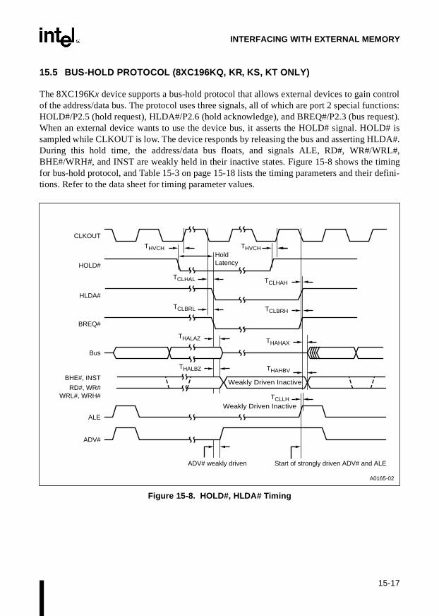
15-17
INTERFACING WITH EXTERNAL MEMORY
15.5 BUS-HOLD PROTOCOL (8XC196KQ, KR, KS, KT ONLY)
The 8XC196Kx device supports a bus-hold protocol that allows external devices to gain controlof the address/data bus. The protocol uses three signals, all of which are port 2 special functions:HOLD#/P2.5 (hold request), HLDA#/P2.6 (hold acknowledge), and BREQ#/P2.3 (bus request).When an external device wants to use the device bus, it asserts the HOLD# signal. HOLD# issampled while CLKOUT is low. The device responds by releasing the bus and asserting HLDA#.During this hold time, the address/data bus floats, and signals ALE, RD#, WR#/WRL#,BHE#/WRH#, and INST are weakly held in their inactive states. Figure 15-8 shows the timingfor bus-hold protocol, and Table 15-3 on page 15-18 lists the timing parameters and their defini-tions. Refer to the data sheet for timing parameter values.
Figure 15-8. HOLD#, HLDA# Timing
CLKOUT
HOLD#
HLDA#
BREQ#
Bus
BHE#, INST
RD#, WR# WRL#, WRH#
ALE
TCLLH
TCLHAH
TCLBRH
THAHAX
THAHBVTHALBZ
THALAZ
TCLBRL
TCLHAL
THVCH THVCHHold Latency
Weakly Driven Inactive
ADV#
ADV# weakly driven Start of strongly driven ADV# and ALE
A0165-02
Weakly Driven Inactive

8XC196Kx, Jx, CA USER’S MANUAL
15-18
When the external device is finished with the bus, it relinquishes control by driving HOLD# high.In response, the 8XC196Kx drives HLDA# high and assumes control of the bus.
If the 8XC196Kx has a pending external bus cycle while it is in hold, it asserts BREQ# to requestcontrol of the bus. After the external device responds by driving HOLD# high, the 8XC196Kxexits hold and then deasserts BREQ# and HLDA#.
NOTE
If the 8XC196Kx receives an interrupt request while it is in hold, the 8XC196Kx asserts INTOUT# only if it is executing from internal memory. If the 8XC196Kx needs to access external memory, it asserts BREQ# and waits until the external device deasserts HOLD# to assert INTOUT#. If the 8XC196Kx receives an interrupt request as it is going into hold (between the time that an external device asserts HOLD# and the time that the 8XC196Kx responds with HLDA#), the 8XC196Kx asserts INTOUT# and keeps it asserted until the external device deasserts HOLD#.
15.5.1 Enabling the Bus-hold Protocol (8XC196K x Only)
To use the bus-hold protocol, you must configure P2.3/BREQ#, P2.5/HOLD#, and P2.6/HLDA#to operate as special-function signals. BREQ# and HLDA# are active-low outputs; HOLD# is anactive-low input.
Table 15-3. HOLD#, HLDA# Timing Def init ions
Symbol Parameter
THVCH HOLD# Setup Time
TCLHAL CLKOUT Low to HLDA# Low
TCLHAH CLKOUT Low to HLDA# High
TCLBRL CLKOUT Low to BREQ# Low
TCLBRH CLKOUT Low to BREQ# High
THALAZ HLDA# Low to Address Float
THAHAX HLDA# High to Address No Longer Float
THALBZ HLDA# Low to BHE#, INST, RD#, WR#, WRL#, WRH# Weakly Driven
THAHBV HLDA# High to BHE#, INST, RD#, WR#, WRL#, WRH# valid
TCLLH Clock Falling to ALE Rising; Use to derive other timings.

15-19
INTERFACING WITH EXTERNAL MEMORY
You must also set the hold enable bit (HLDEN) in the window selection register (WSR.7) to en-able the bus-hold protocol. Once the bus-hold protocol has been selected, the port functions ofP2.3, P2.5, and P2.6 cannot be selected without resetting the device. (During the time that the pinsare configured to operate as special-function signals, their special-function values can be readfrom the P2_PIN.x bits.) However, the hold function can be dynamically enabled and disabled asdescribed in “Disabling the Bus-hold Protocol (8XC196Kx Only).”
15.5.2 Disabling the Bus-hold Protocol (8XC196K x Only)
To disable hold requests, clear WSR.7. The device does not take over the bus immediately afterHLDEN is cleared. Instead, it waits for the current HOLD# request to finish and then disables thebus-hold feature and ignores any new requests until the bit is set again.
Sometimes it is important to prevent another device from taking control of the bus while a blockof code is executing. One way to protect a code segment is to clear WSR.7 and then execute aJBC instruction to check the status of the HLDA# signal. The JBC instruction prevents the RALUfrom executing the protected block until current HOLD# requests are serviced and the hold fea-ture is disabled. This is illustrated in the following code:
DI ;Disable interrupts to prevent ;code interruption
PUSH WSR ;Disable hold requests andLDB WSR,#1FH ;window Port 2
WAIT: JBC P2_PIN,6, WAIT ;Check the HLDA# signal. If set,;add protected instruction here
POP WSR ;Enable hold requestsEI ;Enable interrupts
15.5.3 Hold Latency (8XC196K x Only)
When an external device asserts HOLD#, the device finishes the current bus cycle and then as-serts HLDA#. The time it takes the device to assert HLDA# after the external device assertsHOLD# is called hold latency (see Figure 15-8). Table 15-4 lists the maximum hold latency foreach type of bus cycle.
Table 15-4. Maximum Hold Latency
Bus Cycle Type Maximum Hold Latency(state times)
Internal execution or idle mode 1.5
16-bit external execution 2.5 + 1 per wait state
8-bit external execution 2.5 + 2 per wait state

8XC196Kx, Jx, CA USER’S MANUAL
15-20
15.5.4 Regaining Bus Control (8XC196K x Only)
While HOLD# is asserted, the device continues executing code until it needs to access the exter-nal bus. If executing from internal memory, it continues until it needs to perform an externalmemory cycle. If executing from external memory, it continues executing until the queue is emp-ty or until it needs to perform an external data cycle. As soon as it needs to access the externalbus, the device asserts BREQ# and waits for the external device to deassert HOLD#. After assert-ing BREQ#, the device cannot respond to any interrupt requests, including NMI, until the exter-nal device deasserts HOLD#. One state time after HOLD# goes high, the device deassertsHLDA# and, with no delay, resumes control of the bus.
If the device is reset while in hold, bus contention can occur. For example, a CPU-only devicewould try to fetch the chip configuration byte from external memory after RESET# was broughthigh. Bus contention would occur because both the external device and the device would attemptto access memory. One solution is to use the RESET# signal as the system reset; then all bus mas-ters (including the device) are reset at once. Chapter 13, “Minimum Hardware Considerations,”shows system reset circuit examples.
15.6 BUS-CONTROL MODES
The ALE and WR bits (CCR0.3 and CCR0.2) define which bus-control signals will be generatedduring external read and write cycles. Table 15-5 lists the four bus-control modes and shows theCCR0.3 and CCR0.2 settings for each..
15.6.1 Standard Bus-control Mode
In the standard bus-control mode, the device generates the standard bus-control signals: ALE,RD#, WR#, and BHE# (see Figure 15-9). ALE is asserted while the address is driven, and it canbe used to latch the address externally. RD# is asserted for every external memory read, and WR#is asserted for every external memory write. When asserted, BHE# selects the bank of memorythat is addressed by the high byte of the data bus.
Table 15-5. Bus-control Mode
Bus-control Mode Bus-control Signals CCR0.3(ALE)
CCR0.2(WR)
Standard Bus-control Mode ALE, RD#, WR#, BHE#† 1 1
Write Strobe Mode ALE, RD#, WRL#, WRH#† 1 0
Address Valid Strobe Mode ADV#, RD#, WR#, BHE#† 0 1
Address Valid with Write Strobe Mode ADV#, RD#, WRL#, WRH#† 0 0
† The BHE# and WRH# pins are not implemented on the 87C196CA, 8XC196Jx devices.

15-21
INTERFACING WITH EXTERNAL MEMORY
Figure 15-9. Standard Bus Control
When the device is configured to use a 16-bit bus, separate low- and high-byte write signals mustbe generated for single-byte writes. Figure 15-10 shows a sample circuit that combines BHE# andAD0 to produce these signals (WRL# and WRH#). A similar pair of signals for read is unneces-sary. For a single-byte read with the 16-bit bus, both bytes are placed on the data bus and the pro-cessor discards the unwanted byte.
Figure 15-10. Decoding WRL# and WRH#
ALE
WR# or RD#
BHE#
AD15:0
Valid
Addr Data Out
16-bit Bus Cycle
ALE
WR# or RD#
AD7:0
AD15:8 Address High
Addr Low Data Out
8-bit Bus Cycle
A3077-01
BHE#
WR#
AD0
WRH#
WRL#
A3109-01
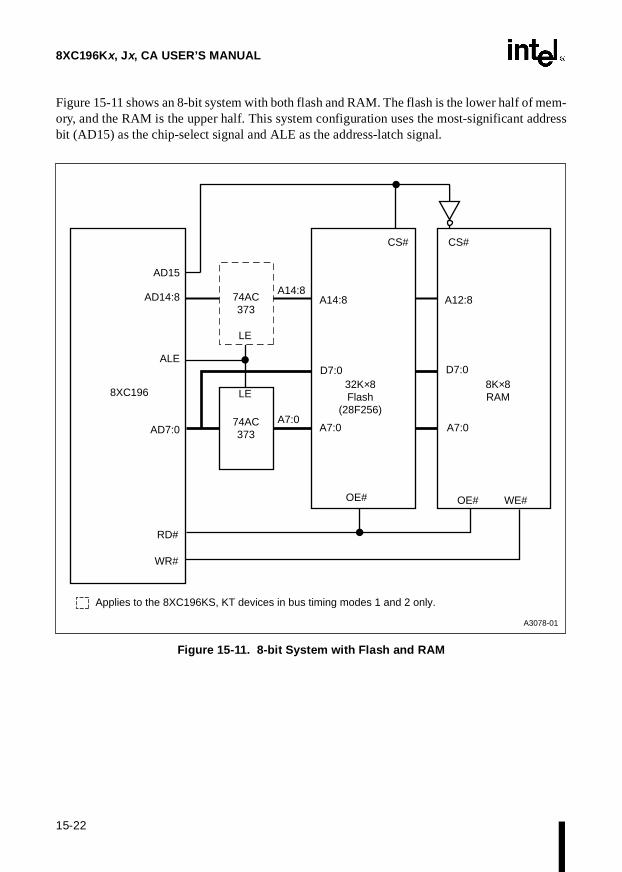
8XC196Kx, Jx, CA USER’S MANUAL
15-22
Figure 15-11 shows an 8-bit system with both flash and RAM. The flash is the lower half of mem-ory, and the RAM is the upper half. This system configuration uses the most-significant addressbit (AD15) as the chip-select signal and ALE as the address-latch signal.
Figure 15-11. 8-bit System with Flash and RAM
AD14:8
AD7:0
ALE
RD#
WR#
8XC196
74AC 373
32K×8 Flash
(28F256)
8K×8 RAM
A7:0
A14:8
D7:0
OE# OE# WE#
CS# CS#
A3078-01
A7:0
D7:0
A12:8
AD15
LE
A7:0
74AC 373
LE
A14:8
Applies to the 8XC196KS, KT devices in bus timing modes 1 and 2 only.

15-23
INTERFACING WITH EXTERNAL MEMORY
Figure 15-12 shows a system that uses the dynamic bus-width feature. (The CCR bits, BW0 andBW1, are set.) Code is executed from the two EPROMs and data is stored in the byte-wide RAM.The RAM is in high memory. It is selected by driving AD15 high, which also selects the 8-bit buswidth mode by driving the BUSWIDTH signal low.
Figure 15-12. 16-bit System with Dynamic Bus Width
A3087-01
AD15:8
RD#
ALE
74AC 373
74AC 373
A13:7
A6:0
CS# CS#
OE# OE#
8XC196
16K×8 EPROM (High)
16K×8 EPROM
(Low)
D7:0
CS#
OE#
8K×8 RAM
WE#
WR#
BUSWIDTH
AD7:0
LE
LE
A13:7 A12:8
A6:0 A7:0
D7:0
D15:8
A7:1 A7:1 A7:0
A14:8 A14:8 A12:8
A15

8XC196Kx, Jx, CA USER’S MANUAL
15-24
15.6.2 Write Strobe Mode
The write strobe mode eliminates the need to externally decode high- and low-byte writes to ex-ternal 16-bit RAM in 16-bit bus mode. When the write strobe mode is selected, the device gen-erates WRL# and WRH# instead of WR# and BHE#. WRL# is asserted for all low byte writes(even addresses) and all word writes. WRH# is asserted for all high byte writes (odd addresses)and all word writes. In the 8-bit bus mode, WRH# and WRL# are asserted for both even and oddaddresses. Figure 15-13 shows write strobe mode timing.
Figure 15-13. Write Strobe Mode
ALE
WRL#
WRH#
AD15:0
Valid
Address Data Out
16-bit Bus Cycle
ALE
WRL# and WRH#
AD7:0
AD15:8 Address High
Address Low Data Out
8-bit Bus Cycle
Valid
A3089-01
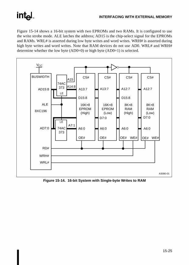
15-25
INTERFACING WITH EXTERNAL MEMORY
Figure 15-14 shows a 16-bit system with two EPROMs and two RAMs. It is configured to usethe write strobe mode. ALE latches the address; AD15 is the chip-select signal for the EPROMsand RAMs. WRL# is asserted during low byte writes and word writes. WRH# is asserted duringhigh byte writes and word writes. Note that RAM devices do not use AD0. WRL# and WRH#determine whether the low byte (AD0=0) or high byte (AD0=1) is selected.
Figure 15-14. 16-bit System with Single-byte Writes to RAM
A3090-01
AD15:8
ALE
AD7:0
8XC196
RD#
WRH#
WRL#
74AC 373
74AC 373
CS#
OE#
CS#
OE#
CS#
OE# WE#
CS#
OE# WE#
8K×8 RAM (Low)
D7:0
A6:0
D7:0
A6:0
8K×8 RAM (High)
D15:8
A6:0
16K×8 EPROM
(Low)
16K×8 EPROM (High)
D15:8
A6:0
BUSWIDTH
VCC
A12:7A12:7A13:7 A13:7
A7:1
A14:8
LE
LE
A15

8XC196Kx, Jx, CA USER’S MANUAL
15-26
15.6.3 Address Valid Strobe Mode
When the address valid strobe mode is selected, the device generates the address valid signal(ADV#) instead of the address latch enable signal (ALE). ADV# is asserted after an external ad-dress is valid (see Figure 15-15). This signal can be used to latch the valid address and simulta-neously enable an external memory device.
Figure 15-15. Address Valid Strobe Mode
The difference between ALE and ADV# is that ADV# is asserted for the entire bus cycle, not justto latch the address. Figure 15-16 shows the difference between ALE and ADV# for a single reador write cycle. Note that for back-to-back bus access, the ADV# function will look identical tothe ALE function. The difference becomes apparent only when the bus is idle. Because ADV# ishigh during these periods, external memory will be disabled, thus saving power.
Figure 15-16. Comparison of ALE and ADV# Bus Cycles
ADV#
WR# or RD#
BHE#
AD15:0
Valid
Data OutAddress
16-bit Bus Cycle 8-bit Bus Cycle
Address High
Data Out
ADV#
WR# or RD#
AD7:0
AD15:0
Addr Low
A3092-01
Address Data
ADV#
ALE
RD#/WR#
Next Bus CycleBus Idle
A3093-01
AD15:0

15-27
INTERFACING WITH EXTERNAL MEMORY
Figure 15-17 and Figure 15-18 show sample circuits that use address valid strobe mode. Figure15-17 shows a simple 8-bit system with a single flash. It is configured for the address valid strobemode. This system configuration uses the ADV# signal as both the flash chip-select signal andthe address-latch signal.
Figure 15-17. 8-bit System with Flash
A3132-01
RD#
AD14:8
AD7:0
8XC196 32K×8 Flash
(28F256)
74AC 373
A14:8
OE#
D7:0
A7:0A7:0
LE
ADV#
74AC 373
CS#
A14:8
LE
Applies to the 8XC196KS, KT devices in bus timing modes 1 and 2 only.

8XC196Kx, Jx, CA USER’S MANUAL
15-28
Figure 15-18 shows a 16-bit system with two EPROMs. This system configuration uses theADV# signal as both the EPROM chip-select signal and the address-latch signal.
Figure 15-18. 16-bit System with EPROM
A3095-01
VCC
AD7:0
AD15:8
RD#
ADV#
74AC 373
74AC 373
A13:7 A13:7
D15:8
D7:0
A6:0 A6:0
CS# CS#
OE# OE#
8XC19616K×8
EPROM (High)
16K×8 EPROM
(Low)
BUSWIDTH
A7:1 A7:1
A14:8 A15:8
LE
LE

15-29
INTERFACING WITH EXTERNAL MEMORY
15.6.4 Address Valid with Write Strobe Mode
When the address valid with write strobe mode is selected, the device generates the ADV#,WRL#, and WRH# bus-control signals. This mode is used for a simple system using external 16-bit RAM. Figure 15-19 shows the timing. The RD# signal (not shown) is similar to WRL#,WRH#, and WR#. The example system of Figure 15-20 uses address valid with write strobe.
Figure 15-19. Timings of Address Valid with Write Strobe Mode
ADV#
WRH#
AD15:0
Valid
Data OutAddress
16-bit Bus Cycle 8-bit Bus Cycle
Address High
Addr Low
Data Out
ADV#
WRL#
AD7:0
AD15:0
ValidWRL#
A3096-01

8XC196Kx, Jx, CA USER’S MANUAL
15-30
Figure 15-20. 16-bit System with RAM
15.7 BUS TIMING MODES (8XC196KS, KT ONLY)
The 8XC196KS, KT devices have selectable bus timing modes controlled by the MSEL0 andMSEL1 bits (bits 6 and 7) of CCR1. Figure 15-2 on page 15-7 defines these bit settings. The re-mainder of this section describes each mode. Figure 15-21 illustrates the modes together and Ta-ble 15-6 summarizes the differences in their timings.
AD7:0
AD15:8
WRL#
ADV#
74AC 373
74AC 373
A12:7 A12:7
D15:8
D7:0
A6:0 A6:0
CS# CS#
WE# WE#
8XC1968K×8 RAM (High)
8K×8 RAM (Low)
WRH#
BUSWIDTH
VCC
A3097-01
A7:1
A13:8
LE
LE
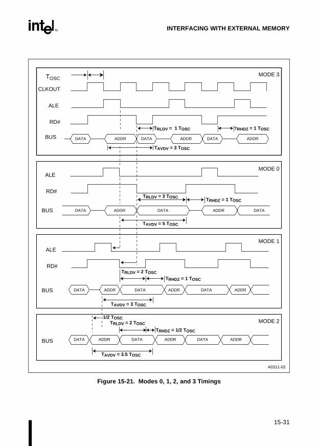
15-31
INTERFACING WITH EXTERNAL MEMORY
Figure 15-21. Modes 0, 1, 2, and 3 Timings
TOSC
CLKOUT
ALE
BUS
RD#
RD#
ALE
RD#
BUS
BUS
BUS
MODE 3
MODE 0
MODE 1
MODE 2
TRLDV = 1 TOSC
TAVDV = 3 TOSC
TRLDV = 2 TOSC
TRLDV = 3 TOSC
TAVDV = 3 TOSC
TAVDV = 3.5 TOSC
TRHDZ = 1/2 TOSC
1/2 TOSC
TAVDV = 5 TOSC
TRHDZ = 1 TOSC
TRHDZ = 1 TOSC
DATA DATA DATAADDR ADDR
DATA DATA DATAADDR ADDR
DATA ADDR
DATA ADDRDATA ADDRDATA ADDR
DATA ADDRDATA ADDR
ADDR
ALE
TRHDZ = 1 TOSC
A0311-02
TRLDV = 2 TOSC
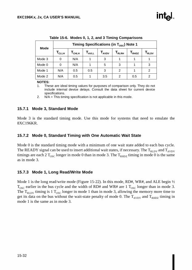
8XC196Kx, Jx, CA USER’S MANUAL
15-32
15.7.1 Mode 3, Standard Mode
Mode 3 is the standard timing mode. Use this mode for systems that need to emulate the8XC196KR.
15.7.2 Mode 0, Standard Timing with One Automatic Wait State
Mode 0 is the standard timing mode with a minimum of one wait state added to each bus cycle.The READY signal can be used to insert additional wait states, if necessary. The TRLDV and TAVDV
timings are each 2 TOSC longer in mode 0 than in mode 3. The TRHDZ timing in mode 0 is the sameas in mode 3.
15.7.3 Mode 1, Long Read/Write Mode
Mode 1 is the long read/write mode (Figure 15-22). In this mode, RD#, WR#, and ALE begin ½TOSC earlier in the bus cycle and the width of RD# and WR# are 1 TOSC longer than in mode 3.The TRLDV timing is 1 TOSC longer in mode 1 than in mode 3, allowing the memory more time toget its data on the bus without the wait-state penalty of mode 0. The TAVDV and TRHDZ timing inmode 1 is the same as in mode 3.
Table 15-6. Modes 0, 1, 2, and 3 Timing Comparisons
ModeTiming Specifications (in T OSC) Note 1
TCLLH TCHLH TAVLL TAVDV TRLRH TRHDZ TRLDV
Mode 3 0 N/A 1 3 1 1 1
Mode 0 0 N/A 1 5 3 1 3
Mode 1 N/A 0.5 0.5 3 2 1 2
Mode 2 N/A 0.5 1 3.5 2 0.5 2
NOTES:1. These are ideal timing values for purposes of comparison only. They do not
include internal device delays. Consult the data sheet for current devicespecifications.
2. N/A = This timing specification is not applicable in this mode.

15-33
INTERFACING WITH EXTERNAL MEMORY
Figure 15-22. Mode 1 System Bus Timing
15.7.4 Mode 2, Long Read/Write with Early Address
Mode 2 (Figure 15-23) is similar to mode 1 in that RD#, WR#, and ALE begin ½ TOSC earlier inthe bus cycle and the widths of RD# and WR# are 1 TOSC longer than in mode 3. It differs frommode 1 in that the address is also placed onto the bus ½ TOSC earlier in the bus cycle. The TRLDV
timing is 1 TOSC longer, the TAVDV timing is ½ TOSC longer, and TRHDZ is ½ TOSC shorter in mode 2than in mode 3. This mode trades a longer TAVDV for a shorter TRHDZ.
XTAL 1
CLKOUT
TCLCL
TLHLH
TRHLHTRLRH
TLLRLTLHLL
TRLDV
TRHDZ
TLLAXTAVLL
TAVDV
TLLWLTWLWH
Address Out Data Out
TQVWH TWHQX
TOSC
TCLLL
Data In D15:0
TCHLH
Address
TXHCHTCHCL
Bus WriteAD15:0
8- and 16-bit Bus Mode
TWHBX, TRHBX
TWHAX, TRHAX
TWHIX, TRHIX
AD15:8
INST
BHE Valid
INST Valid
TRLAZ
ALE/ADV#
RD#
AD15:8 Valid 8-bit Bus Mode
BHE#
WR#
Bus ReadAD15:0
8- and16-bit Bus Mode
A3098-01

8XC196Kx, Jx, CA USER’S MANUAL
15-34
15.7.5 Design Considerations
In all bus timing modes, for 16-bit bus-width operation, latch the upper and lower address/datalines. In modes 1 and 2, for 8-bit bus-width operation, also latch the upper and lower address/datalines; the upper address lines are not driven throughout the entire bus cycle (see Figures 15-22and 15-23). In modes 0 and 3, for 8-bit bus-width operation, latch only the lower address/datalines. In these modes, it is not necessary to latch the upper address lines because these lines aredriven throughout the entire bus cycle.

15-35
INTERFACING WITH EXTERNAL MEMORY
Figure 15-23. Mode 2 System Bus Timing
XTAL 1
CLKOUT
TCLCL
TLHLH
TRHLHTRLRH
TLLRLTLHLL
TRLDV
TRHDZTLLAXTAVLL
TAVDV
TLLWLTWLWH
Address Out Data Out
TQVWH TWHQX
TOSC
TCLLL
Data In D15:0
TCHLH
Address
TXHCHTCHCL
Bus WriteAD15:0
8- and 16-bit Bus Mode
TWHBX, TRHBX
TWHAX, TRHAX
TWHIX, TRHIX
AD15:0
INST
BHE Valid
INST Valid
TRLAZ
ALE/ADV#
RD#
AD15:8 Valid 8-bit Bus Mode
BHE#
WR#
Bus ReadAD15:0
8- and 16-bit Bus Mode
A3099-01

8XC196Kx, Jx, CA USER’S MANUAL
15-36
15.8 SYSTEM BUS AC TIMING SPECIFICATIONS
Refer to the latest data sheet for the AC timings to make sure your system meets specifications.The major external bus timing specifications are shown in Figure 15-24.
Figure 15-24. System Bus Timing
XTAL1
CLKOUT
ALE/ADV#
RD#
WR#
BHE#, INST
TOSC
TXHCH TCHCLTCLCL
TCLLH TLLCHTLHLH
TLHLLTLLRL TRLRH
TRHLH
TRHDZTAVLL
TLLAX TRLDVAddress Out Data In
TAVDV TLLWL TWLWHTWHLH
TQVWH TWHQX
Data OutAddress Out Address Out
Valid
Address Out
TWHBX, TRHBX
TWHAX, TRHAX
TRLAZ
A3100-01
BUS (Read Cycle)
BUS (Write Cycle)
AD15:8 (8-bit Mode)

15-37
INTERFACING WITH EXTERNAL MEMORY
Each symbol consists of two pairs of letters prefixed by “T” (for time). The characters in a pairindicate a signal and its condition, respectively. Symbols represent the time between the two sig-nal/condition points. For example, TCLDV is the time between signal C (CLKOUT) condition L(Low) and signal D (Input Data) condition V (Valid). Table 15-7 defines the signal and conditioncodes.
Table 15-8 defines the AC timing specifications that the memory system must meet and those thatthe device will provide.
Table 15-7. AC Timing Symbol Definitions
Signals Conditions
A Address G BUSWIDTH R RD# H High
B BHE# H HOLD# W WR#, WRH#, WRL# L Low
BR BREQ# HA HLDA# X XTAL1 V Valid
C CLKOUT L ALE/ADV# Y READY X No Longer Valid
D DATA Q Data Out Z Floating
Table 15-8. AC Timing Definit ions
Symbol Definition
The External Memory System Must Meet These Specifications
TAVDV Address Valid to Input Data Valid
Maximum time the memory device has to output valid data after the 87C196CA, 8XC196Jx, Kx outputs a valid address.
TAVGV Address Valid to BUSWIDTH† Valid
Maximum time after address is valid until BUSWIDTH must be valid. If this specification is exceeded, the 8XC196Kx may not respond with the specified bus cycle.
TAVYV Address Valid to READY†† Setup
Maximum time the memory system has to assert READY after the 87C196CA, 8XC196Kx outputs the address to guarantee that at least one wait state will occur.
TCLDV CLKOUT Low to Input Data Valid
Maximum time the memory system has to output valid data after CLKOUT falls.
TCLGX BUSWIDTH† Hold after CLKOUT Low
Minimum time BUSWIDTH must be held valid after CLKOUT falls. Always 0 ns on the 8XC196Kx.
TCLYX READY†† Hold after CLKOUT Low
Minimum hold time is always 0 ns. If maximum specification is exceeded, additional wait states will occur.
† 8XC196Kx only; the BUSWIDTH and BHE# pins are not implemented on the 87C196CA, 8XC196Jx. †† 8XC196Kx, 87C196CA only; the READY and INST pins are not implemented on the 8XC196Jx.

8XC196Kx, Jx, CA USER’S MANUAL
15-38
The External Memory System Must Meet These Specifications (Continued)
TLLGV ALE Low to BUSWIDTH† Valid
Maximum time after ALE/ADV# falls until BUSWIDTH must be valid. If this specification is exceeded, the 8XC196Kx may not respond with the specified bus cycle.
TLLYH ALE Low to READY†† Setup
Maximum time the memory system has to assert READY after ALE falls to guarantee that at least one wait state will occur. (This specification is included only for comparison with HMOS device timings.)
TLLYX READY†† Hold after ALE Low
Minimum time the level of the READY signal must be valid after ALE falls. If the maximum value is exceeded, additional wait states will occur.
TRHDX Data Hold after RD# High
Time after RD# is inactive that the memory system must hold data on the bus. Always 0 ns.
TRHDZ RD# High to Input Data Float
Time after RD# is inactive until the memory system must float the bus. If this timing is not met, bus contention will occur.
TRLDV RD# Low to Input Data Valid
Maximum time the memory system has to output valid data after the 87C196CA, 8XC196Jx, Kx asserts RD#.
The 87C196CA, 8XC196J x, Kx Meets These Specifications
FXTAL Frequency on XTAL
Frequency of the signal input on the XTAL1 input. The internal bus speed of the 87C196CA, 8XC196Jx, Kx device is ½ FXTAL.
TOSC 1/FXTAL
All AC Timings are referenced to TOSC.
TAVLL Address Setup to ALE/ADV# Low: Length of time address is valid before ALE/ADV# falls. Use this specification when designing the external latch.
TCHCL CLKOUT High Period
Needed in systems that use CLKOUT as clock for external devices.
TCHLH CLKOUT High to ALE/ADV# High (8XC196KS, KT, modes 1 and 2 only)
Time between CLKOUT going high and ALE/ADV# going high. Use to derive other timings.
TCHWH CLKOUT High to WR# High
Time between CLKOUT going high and WR# going inactive.
TCLCL CLKOUT Cycle Time
Normally 2 TOSC.
TCLLH CLKOUT Falling to ALE/ADV# Rising
Use to derive other timings.
Table 15-8. AC Timing Definitions (Continued)
Symbol Definition
† 8XC196Kx only; the BUSWIDTH and BHE# pins are not implemented on the 87C196CA, 8XC196Jx. †† 8XC196Kx, 87C196CA only; the READY and INST pins are not implemented on the 8XC196Jx.
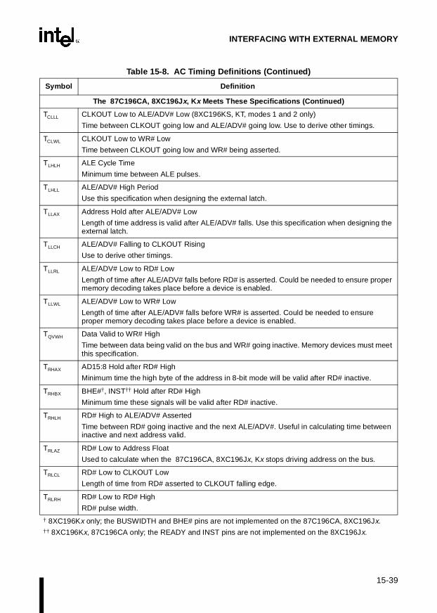
15-39
INTERFACING WITH EXTERNAL MEMORY
The 87C196CA, 8XC196J x, Kx Meets These Specifications (Continued)
TCLLL CLKOUT Low to ALE/ADV# Low (8XC196KS, KT, modes 1 and 2 only)
Time between CLKOUT going low and ALE/ADV# going low. Use to derive other timings.
TCLWL CLKOUT Low to WR# Low
Time between CLKOUT going low and WR# being asserted.
TLHLH ALE Cycle Time
Minimum time between ALE pulses.
TLHLL ALE/ADV# High Period
Use this specification when designing the external latch.
TLLAX Address Hold after ALE/ADV# Low
Length of time address is valid after ALE/ADV# falls. Use this specification when designing the external latch.
TLLCH ALE/ADV# Falling to CLKOUT Rising
Use to derive other timings.
TLLRL ALE/ADV# Low to RD# Low
Length of time after ALE/ADV# falls before RD# is asserted. Could be needed to ensure proper memory decoding takes place before a device is enabled.
TLLWL ALE/ADV# Low to WR# Low
Length of time after ALE/ADV# falls before WR# is asserted. Could be needed to ensure proper memory decoding takes place before a device is enabled.
TQVWH Data Valid to WR# High
Time between data being valid on the bus and WR# going inactive. Memory devices must meet this specification.
TRHAX AD15:8 Hold after RD# High
Minimum time the high byte of the address in 8-bit mode will be valid after RD# inactive.
TRHBX BHE#†, INST†† Hold after RD# High
Minimum time these signals will be valid after RD# inactive.
TRHLH RD# High to ALE/ADV# Asserted
Time between RD# going inactive and the next ALE/ADV#. Useful in calculating time between inactive and next address valid.
TRLAZ RD# Low to Address Float
Used to calculate when the 87C196CA, 8XC196Jx, Kx stops driving address on the bus.
TRLCL RD# Low to CLKOUT Low
Length of time from RD# asserted to CLKOUT falling edge.
TRLRH RD# Low to RD# High
RD# pulse width.
Table 15-8. AC Timing Definitions (Continued)
Symbol Definition
† 8XC196Kx only; the BUSWIDTH and BHE# pins are not implemented on the 87C196CA, 8XC196Jx. †† 8XC196Kx, 87C196CA only; the READY and INST pins are not implemented on the 8XC196Jx.

8XC196Kx, Jx, CA USER’S MANUAL
15-40
The 87C196CA, 8XC196J x, Kx Meets These Specifications (Continued)
TWHAX AD15:8 Hold after WR# High
Minimum time the high byte of the address in 8-bit mode will be valid after WR# inactive.
TWHBX BHE#†, INST†† Hold after WR# High
Minimum time these signals will be valid after WR# inactive. (8XC196Kx only)
TWHLH WR# High to ALE/ADV# High
Time between WR# going inactive and next ALE/ADV#. Also used to calculate WR# inactive and next address valid.
TWHQX Data Hold after WR# High
Length of time after WR# rises that the data stays valid on the bus. Memory devices must meet this specification.
TWLWH WR# Low to WR# High
WR# pulse width.
TXHCH XTAL1 High to CLKOUT High or Low
Table 15-8. AC Timing Definitions (Continued)
Symbol Definition
† 8XC196Kx only; the BUSWIDTH and BHE# pins are not implemented on the 87C196CA, 8XC196Jx. †† 8XC196Kx, 87C196CA only; the READY and INST pins are not implemented on the 8XC196Jx.

16Programming the Nonvolatile Memory


16-1
CHAPTER 16PROGRAMMING THE NONVOLATILE MEMORY
The 87C196Kx devices contain from 12 Kbytes to 48 Kbytes of one-time-programmable read-only memory (OTPROM). Table 16-1 lists the devices and OTPROM sizes. OTPROM is similarto EPROM, but it comes in an unwindowed package and cannot be erased. You can either pro-gram the OTPROM yourself or have the factory program it as a quick-turn ROM product (thisoption may not be available for all devices). This chapter provides procedures and guidelines tohelp you program the device. The information is organized as follows.
• overview of programming methods (page 16-2)
• OTPROM memory map (page 16-2)
• security features (page 16-3)
• programming pulse width (page 16-8)
• modified quick-pulse algorithm (page 16-10)
• programming mode pins (page 16-11)
• entering programming modes (page 16-14)
• slave programming (page 16-15)
• auto programming (page 16-26)
• serial port programming (page 16-32)
• run-time programming (page 16-44)
NOTE
Some devices may also be available in windowed EPROM packages. In this manual, OTPROM refers to the device’s internal read-only memory, whether it is EPROM or OTPROM, and EPROM refers specifically to EPROM devices.
Table 16-1. OTPROM Sizes for 87C196K x, Jx, CA Devices
87C196JQ, KQ 87C196JR, KR 87C196KS † 87C196CA, JT†, KT 87C196JV†
12 Kbytes(2000–4FFFH)
16 Kbytes(2000–5FFFH)
24 Kbytes(2000–7FFFH)
32 Kbytes(2000–9FFFH)
48 Kbytes(2000–DFFFH)
†The 8XC196JT, JV, and KS are offered in automotive temperature ranges only. The 8XC196CA, JQ, JR, KQ, KR, and KT are offered in both automotive and commercial temperature ranges.

8XC196Kx, Jx, CA USER’S MANUAL
16-2
16.1 PROGRAMMING METHODS
You can program the OTPROM by configuring a circuit that allows the device to enter a program-ming mode. In programming modes, the device executes an algorithm that resides in the internaltest ROM.
• Slave programming mode allows you to use an EPROM programmer as a master toprogram 8XC196 devices (the slaves). The code and data to be programmed into thenonvolatile memory typically resides on a diskette. The EPROM programmer transfers thecode and data from the diskette to its memory, then manipulates the slave’s pins to definethe addresses to be programmed and the contents to be written to those addresses. Using thismode, you can program and verify single or multiple words in the OTPROM. This is theonly mode that allows you to read the signature word and programming voltages and toprogram the PCCBs and unerasable PROM (UPROM) bits. Programming vendors and Inteldistributors typically use this mode to program a large number of microcontrollers with acustomer’s code and data.
• Auto programming mode enables the 8XC196 device to act as a master to program itselfwith code and data that reside in an external memory device. Using this mode, you canprogram the entire OTPROM array except the UPROM bits and PCCBs. Afterprogramming, you can use the ROM-dump mode to write the entire OTPROM array to anexternal memory device to verify its contents. Customers typically use this low-cost methodto program a small number of microcontrollers after development and testing are complete.
• Serial port programming mode enables you to download code and data (usually from apersonal computer or workstation) to an 8XC196 device (the slave) through the serial I/Oport. You can write data to the OTPROM asynchronously via the TXD (P2.0) pin and readthe data via the RXD (P2.1) pin. Customers typically use this mode to download largesections of code to the microcontroller during software development and testing.
You can also program individual OTPROM locations without entering a programming mode.With this method, called run-time programming, your software controls the number and durationof programming pulses. Customers typically use this mode to download small sections of code tothe microcontroller during software development and testing.
16.2 OTPROM MEMORY MAP
The OTPROM contains customer-specified special-purpose and program memory (Table 16-2).The 128-byte special-purpose memory partition is used for interrupt vectors, the chip configura-tion bytes (CCBs), and the security key. Several locations are reserved for testing or for use infuture products. Write the value (20H or FFH) indicated in Table 16-2 to each reserved location.The remainder of the OTPROM is available for code storage.
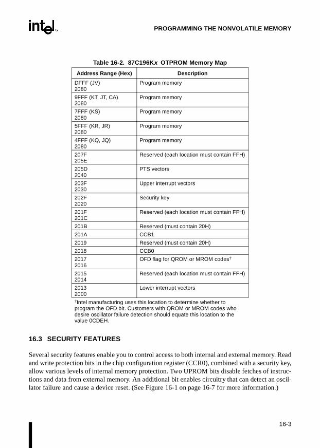
16-3
PROGRAMMING THE NONVOLATILE MEMORY
16.3 SECURITY FEATURES
Several security features enable you to control access to both internal and external memory. Readand write protection bits in the chip configuration register (CCR0), combined with a security key,allow various levels of internal memory protection. Two UPROM bits disable fetches of instruc-tions and data from external memory. An additional bit enables circuitry that can detect an oscil-lator failure and cause a device reset. (See Figure 16-1 on page 16-7 for more information.)
Table 16-2. 87C196K x OTPROM Memory Map
Address Range (Hex) Description
DFFF (JV) 2080
Program memory
9FFF (KT, JT, CA) 2080
Program memory
7FFF (KS)2080
Program memory
5FFF (KR, JR)2080
Program memory
4FFF (KQ, JQ)2080
Program memory
207F205E
Reserved (each location must contain FFH)
205D2040
PTS vectors
203F2030
Upper interrupt vectors
202F2020
Security key
201F201C
Reserved (each location must contain FFH)
201B Reserved (must contain 20H)
201A CCB1
2019 Reserved (must contain 20H)
2018 CCB0
20172016
OFD flag for QROM or MROM codes†
2015 2014
Reserved (each location must contain FFH)
20132000
Lower interrupt vectors
†Intel manufacturing uses this location to determine whether to program the OFD bit. Customers with QROM or MROM codes who desire oscillator failure detection should equate this location to the value 0CDEH.

8XC196Kx, Jx, CA USER’S MANUAL
16-4
16.3.1 Controlling Access to Internal Memory
The lock bits in the chip configuration register (CCR0) control access to the OTPROM. The resetsequence loads the CCRs from the CCBs for normal operation and from the PCCBs when enter-ing programming modes. You can program the CCBs using any of the programming methods, butonly slave programming mode allows you to program the PCCBs.
NOTE
The developers have made a substantial effort to provide an adequate program protection scheme. However, Intel cannot and does not guarantee that these protection methods will always prevent unauthorized access.
16.3.1.1 Controlling Access to the OTPROM Dur ing Normal Operation
During normal operation, the lock bits in CCB0 control read and write accesses to the OTPROM.Table 16-3 describes the options. You can program the CCBs using any of the programmingmethods.
Clearing CCB0.6 enables write protection. With write protection enabled, a write attempt causesthe bus controller to cycle through the write sequence, but it does not enable VPP or write data tothe OTPROM. This protects the entire OTPROM array from inadvertent or unauthorized pro-gramming.
Clearing CCB0.7 enables read protection and also write protects the security key to protect itfrom being overwritten. With read protection enabled, the bus controller will not read from pro-tected areas of OTPROM. An attempt to load the slave program counter with an external addresscauses the device to reset itself. Because the slave program counter can be as much as four bytesahead of the CPU program counter, the bus controller might prevent code execution from the lastfour bytes of internal memory. The interrupt vectors and CCBs are not read protected becauseinterrupts can occur even when executing from external memory.
Table 16-3. Memory Protection for Normal Operating Mode
Read ProtectLOC1 (CCR0.7)
Write ProtectLOC0 (CCR0.6) Protection Status
1 1 No protection. Run-time programming is permitted, and the entire OTPROM array can be read.
1 0 Write protection only. Run-time programming is disabled, but the entire OTPROM array can be read.
0 1 Read protection. Run-time programming is disabled. If program execution is external, only the interrupt vectors and CCBs can be read. The security key is write protected.
0 0 Read and write protection. Run-time programming is disabled. If program execution is external, only the interrupt vectors and CCBs can be read.

16-5
PROGRAMMING THE NONVOLATILE MEMORY
16.3.1.2 Controlling Access to the OTPROM Dur ing Programming Modes
For programming modes, three levels of protection are available:
• prohibit all programming
• prohibit all programming, but permit authorized ROM dumps
• prohibit serial port programming, but permit authorized ROM dumps, auto programming,and slave programming
These protection levels are provided by the PCCB0 lock bits, the CCB0 lock bits, and the internalsecurity key (Table 16-4). When entering programming modes, the reset sequence loads thePCCBs into the chip configuration registers. It also loads CCB0 into internal RAM to provide anadditional level of security.
You can program the CCBs using any of the programming methods, but only slave programmingmode permits access to the PCCBs, and only slave and auto programming allow you to programthe internal security key.
If you want to prohibit all programming, clear both PCCB0 lock bits. If these bits are cleared,they prevent the device from entering any programming mode.
If you want to prevent programming, but allow ROM dumps, leave the PCCB0 read-protectionbit (PCCB0.7) unprogrammed and clear the PCCB0 write-protection lock bit (PCCB0.6). To pro-tect against unauthorized reads, program an internal security key. The ROM-dump mode com-pares the internal security key location with an externally supplied security key regardless of theCCB0 lock bits. If the security keys match, the routine continues; otherwise, the device enters anendless internal loop.
Table 16-4. Memory Protection Options for Programming Modes
LOC1 (CCR0.7)
LOC0(CCR0.6) Security Key
Programmed?
Protection Status
PCCB CCB PCCB CCB
1 1 1 1 No No protection. All programming modes allowed.
1 X 0 X Yes All programming disabled. ROM-dump permitted with matching security key.
X X X X Yes Serial programming disabled.
1 0 1 0 Yes Serial programming disabled. Auto and slave programming permitted with matching security key.
0 X 0 X X All programming unconditionally disabled.

8XC196Kx, Jx, CA USER’S MANUAL
16-6
If you want to allow slave and auto programming as well as ROM dumps, leave both PCCB0 lockbits unprogrammed. To protect against unauthorized programming, clear the CCB0 lock bits andprogram an internal security key. After the device enters either slave or auto programming mode,the corresponding test ROM routine reads the CCB0 lock bits. If either CCB0 lock bit is enabled,the routine compares the internal security key location with an externally supplied security key.If the security keys match, the routine continues; otherwise, the device enters an endless internalloop.
You can program the internal security key in either auto or slave programming mode. Once thesecurity key is programmed, you must provide a matching key to gain access to any programmingmode. For auto programming and ROM-dump modes, a matching security key must reside in ex-ternal memory. For slave programming mode, you must “program” a matching security key intothe appropriate OTPROM locations with the program word command. The locations are not ac-tually programmed, but the data is compared to the internal security key.
The serial programming mode checks the internal security key regardless of the CCB0 lock bits.This mode has no provision for security key verification. If the security key is blank (FFFFH),serial programming continues. If any word contains a value other than FFFFH, the device entersan endless internal loop.
WARNING
If you leave the internal security key locations unprogrammed (filled with FFFFH), an unauthorized person could gain access to the OTPROM by using an external EPROM with an unprogrammed external security key location or by using slave or serial port programming mode.
16.3.2 Controlling Fetches from External Memory
Two UPROM bits disable external instruction fetches and external data fetches. If you programthe UPROM bits, an attempt to fetch data or instructions from external memory causes a devicereset. Another bit enables circuitry that can detect an oscillator failure and cause a device reset.You can program the UPROM bits using slave programming mode.
Programming the DEI bit prevents the bus controller from executing external instruction fetches.An attempt to load the slave program counter with an external address causes the device to resetitself. Because the slave program counter can be as much as four bytes ahead of the CPU programcounter, the bus controller might prevent code execution from the last four bytes of internal mem-ory. The automatic reset also gives extra protection against runaway code.
Programming the DED bit prevents the bus controller from executing external data reads andwrites. An attempt to access data through the bus controller causes the device to reset itself. Set-ting this bit disables ROM-dump mode.

16-7
PROGRAMMING THE NONVOLATILE MEMORY
To program these bits, write the correct value to the location shown in Table 16-5 on page 16-8using slave programming mode. During normal operation, you can determine the values of thesebits by reading the UPROM special-function register (Figure 16-1).
You can verify a UPROM bit to make sure it programmed, but you cannot erase it. For this reason,Intel cannot test the bits before shipment. However, Intel does test the features that the UPROMbits enable, so the only undetectable defects are (unlikely) defects within the UPROM cells them-selves.
USFR Address:Reset State:
1FF6HXXH
The unerasable PROM (USFR) register contains two bits that disable external fetches of data and instructions and another that detects a failed oscillator. These bits can be programmed, but cannot be erased.
WARNING: These bits can be programmed, but can never be erased. Programming these bits makes dynamic failure analysis impossible. For this reason, devices with programmed UPROM bits cannot be returned to Intel for failure analysis.
7 0
— — — — DEI DED — OFD
Bit Number
Bit Mnemonic Function
7:4 — Reserved; always write as zeros.
3 DEI Disable External Instruction Fetch
Setting this bit prevents the bus controller from executing external instruction fetches. Any attempt to load an external address initiates a reset.
2 DED Disable External Data Fetch
Setting this bit prevents the bus controller from executing external data reads and writes. Any attempt to access data through the bus controller initiates a reset.
1 — Reserved; always write as zero.
0 OFD Oscillator Fail Detect
Setting this bit enables the device to detect a failed oscillator and reset itself. (In EPROM packages, this bit can be erased.)
Figure 16-1. Unerasable PROM (USFR) Register

8XC196Kx, Jx, CA USER’S MANUAL
16-8
16.3.3 Enabling the Oscillator Failure Detection Circuitry
Programming the OFD bit enables circuitry that resets the device when it detects a failed oscilla-tor. (See “Detecting Oscillator Failure” on page 13-12 for details.) To program this bit, you mustwrite the correct value to the location shown in Table 16-5, using slave programming mode. Dur-ing normal operation, you can determine the value of this bit by reading the USFR (Figure 16-1on page 16-7). In EPROM packages, the OFD bit can be erased.
16.4 PROGRAMMING PULSE WIDTH
The programming pulse width is controlled in different ways depending on the programmingmode. In all cases, the pulse width must be at least 100 µs for successful programming. In slaveprogramming mode, the pulse width is controlled by the PALE# signal. In auto programmingmode, it is loaded from the external EPROM into the PPW register. In serial port programmingmode, it is loaded from the test ROM into the SP_PPW register. In run-time programming mode,your software controls the pulse width.
The PPW and SP_PPW registers (Figure 16-2) are identical except for their locations and defaultvalues. Both are word registers and both require that the most-significant bit always be set; theremaining bits constitute the PPW_VALUE. To determine the correct PPW_VALUE for the fre-quency of the device, use the following formula and round the result to the next higher integer.
where:
PPW_VALUE is a 15-bit word
FOSC is the input frequency on XTAL1, in MHz
Time is the duration of the programming pulse, in µs
Table 16-5. UPROM Programming Values and Locations for Slave Mode
To set this bit Write this value To this location
DEI 08H 0718H
DED 04H 0758H
OFD† 01H 0778H
†Intel manufacturing uses location 2016H to determine whether to program the OFD bit. Customers with QROM or MROM codes who desire the OFD feature should equate location 2016H to the value 0CDEH.
PPW_VALUEFosc Time×
144-------------------------------- 1–=

16-9
PROGRAMMING THE NONVOLATILE MEMORY
The following two examples calculate the PPW_VALUE for a 100-µs pulse width with an 8-MHzand a 16-MHz crystal, respectively.
You can use the following simplified equation to calculate the PPW_VALUE for a 100-µs pulsewidth at various frequencies:
PPW (or SP_PPW) no direct access
The PPW register is loaded from the external EPROM (locations 14H and 15H) in auto programming mode. The SP_PPW register is loaded from the internal test ROM in serial port programming mode. The default pulse width for serial port programming is longer than required, so you should change the value before beginning to program the device. (See “Changing Serial Port Programming Defaults” on page 16-34.) The PPW_VALUE determines the programming pulse width, which must be at least 100 µs for successful programming.
15 8
1 PPW14 PPW13 PPW12 PPW11 PPW10 PPW9 PPW8
7 0
PPW7 PPW6 PPW5 PPW4 PPW3 PPW2 PPW1 PPW0
Bit Number
BitMnemonic Function
15 1 Set this bit for proper device operation.
14:0 PPW14:0 PPW_VALUE.
This value establishes the programming pulse width for auto programming or serial port programming. For a 100-µs pulse width, use the following formula and round the result to the next higher integer. For auto programming, write this value to the external EPROM (see “Auto Programming Procedure” on page 16-30). For serial port programming, write this value to the internal memory (see “Changing Serial Port Programming Defaults” on page 16-34).
Figure 16-2. Programming Pulse Width Register (PPW or SP_PPW)
PPW_VALUE8 100×
144------------------- 1–
800144---------- 1– 4.5552 5≈ 05H= = = =
PPW_VALUE16 100×
144---------------------- 1–
1600144------------- 1– 10.11 11≈ 0BH= = = =
PPW_VALUE 0.6944 Fosc×( ) 1–=
PPW_VALUE 0.6944 Fosc×( ) 1–=

8XC196Kx, Jx, CA USER’S MANUAL
16-10
16.5 MODIFIED QUICK-PULSE ALGORITHM
Both the slave and auto programming routines use the modified quick-pulse algorithm (Figure16-3). The modified quick-pulse algorithm sends programming pulses to each OTPROM wordlocation. After the required number of programming pulses, a verification routine compares thecontents of the programmed location to the input data. A verification error deasserts the PVERsignal, but does not stop the programming routine. This process repeats until each OTPROMword has been programmed and verified. Intel guarantees lifetime data retention for a device pro-grammed with the modified quick-pulse algorithm.
Figure 16-3. Modified Quick-pulse Algorithm
A0190-03
Return
From Auto or Slave Programming
Required Writes Done
?
Start PPW Timer
Write Data to OTPROM
Enter Idle Mode
Wait for PPW Timer Interrupt
Yes
No
Enable Interrupts
Compare Programmed Locations and Set Flags

16-11
PROGRAMMING THE NONVOLATILE MEMORY
Auto programming repeats the pulse five times, using the pulse width you specify in the externalEPROM. Slave mode repeats the pulse until PROG# is deasserted. In slave programming mode,the PALE# signal controls the pulse width. In all cases, the pulse width must be at least 100 µsfor successful programming.
16.6 PROGRAMMING MODE PINS
Figure 16-4 illustrates the signals used in programming and Table 16-6 describes them. The EA#,VPP, and PMODE pins combine to control entry into programming modes. You must configurethe PMODE (P0.7:4) pins to select the desired programming mode (see Table 16-7 on page16-14). Each programming routine configures the port 2 pins to operate as the appropriate spe-cial-function signals. Ports 3 and 4 automatically serve as the PBUS during programming.
Figure 16-4. Pin Functions in Programming Modes
Table 16-6. Pin Descriptions
Port PinSpecial
Function Signal
TypeProgram-
ming Mode
Description
P0.7:4 PMODE.3:PMODE.0
I All Programming Mode Select
Determines the programming mode. PMODE is sampled after a device reset and must be static while the part is operating. (Table 16-7 on page 16-14 lists the PMODE values and programming modes.)
P2.7
P2.6
P2.4
P2.2
P2.1
P2.0
P4.7:0 P3.7:0
8XC196 Device
PBUS†
A0314-03
P0.7:4 PACT#
CPVER
AINC#
PROG#
PALE#/RXD
PVER/TXD
PMODE.3:04
Programming Voltage
† For auto programming, P1.2:1 replace P4.7:6 as the high address bits.
VPP EA#

8XC196Kx, Jx, CA USER’S MANUAL
16-12
P2.0 PVER O SlaveAuto
Programming Verification
During slave or auto programming, PVER is updated after each programming pulse. A high output signal indicates successful programming of a location, while a low signal indicates a detected error.
TXD O Serial Transmit Serial Data
During serial port programming, TXD transmits data from the OTPROM to an external device.
P2.1 PALE# I Slave Programming ALE Input
During slave programming, a falling edge causes the device to read a command and address from the PBUS.
RXD I Serial Receive Serial Data
During serial port programming, RXD receives data from an external device.
P2.2 PROG# I Slave Programming
During programming, a falling edge latches data on the PBUS and begins programming, while a rising edge ends programming. The current location is programmed with the same data as long as PROG# remains asserted, so the data on the PBUS must remain stable while PROG# is active.
During a word dump, a falling edge causes the contents of an OTPROM location to be output on the PBUS, while a rising edge ends the data transfer.
P2.4 AINC# I Slave Auto-increment
During slave programming, this active-low input enables the auto-increment feature. (Auto increment allows reading or writing of sequential OTPROM locations, without requiring address transactions across the PBUS for each read or write.) AINC# is sampled after each location is programmed or dumped. If AINC# is asserted, the address is incremented and the next data word is programmed or dumped.
P2.6 CPVER O Slave Cumulative Program Verification
During slave programming, a high signal indicates that all locations programmed correctly, while a low signal indicates that an error occurred during one of the programming operations.
P2.7 PACT# O AutoROM-dump
Programming Active
During auto programming or ROM-dump, a low signal indicates that programming or dumping is in progress, while a high signal indicates that the operation is complete.
Table 16-6. Pin Descriptions (Continued)
Port PinSpecial
Function Signal
TypeProgram-
ming Mode
Description
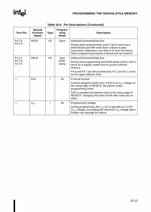
16-13
PROGRAMMING THE NONVOLATILE MEMORY
P4.7:0,P3.7:0
PBUS I/O Slave Address/Command/Data Bus
During slave programming, ports 3 and 4 serve as a bidirectional port with open-drain outputs to pass commands, addresses, and data to or from the device. Slave programming requires external pull-up resistors.
P1.2:1P4.7:5,P3.7:0
PBUS I/O AutoROM-dump
Address/Command/Data Bus
During auto programming and ROM-dump, ports 3 and 4 serve as a regular system bus to access external memory.
P4.6 and P4.7 are left unconnected; P1.2 and P1.1 serve as the upper address lines.
— EA# I All External Access
Controls program mode entry. If EA# is at VPP voltage on the rising edge of RESET#, the device enters programming mode.
EA# is sampled and latched only on the rising edge of RESET#. Changing the level of EA# after reset has no effect.
— VPP I All Programming Voltage
During programming, the VPP pin is typically at +12.5V (VPP voltage). Exceeding the maximum VPP voltage speci-fication can damage the device.
Table 16-6. Pin Descriptions (Continued)
Port PinSpecial
Function Signal
TypeProgram-
ming Mode
Description

8XC196Kx, Jx, CA USER’S MANUAL
16-14
16.7 ENTERING PROGRAMMING MODES
To execute programs properly, the device must have these minimum hardware connections:XTAL1 driven, unused input pins strapped, and power and grounds applied. Follow the operatingconditions specified in the datasheet. Place the device into programming mode by applying VPP
voltage (+12.5 V) to EA# during the rising edge of RESET#.
16.7.1 Selecting the Programming Mode
The PMODE (P0.7:4) value controls the programming mode. PMODE is sampled on the risingedge of RESET#. You must reset the device to switch programming modes. Table 16-7 lists thePMODE value for each programming mode. All other PMODE values are reserved.
16.7.2 Power-up and Power-down Sequences
When you are ready to begin programming, follow these power-up and power-down procedures.
WARNING
Failure to observe these warnings will cause permanent device damage.
• Voltage must not be applied to VPP while VCC is low.
• The VPP voltage must be within 1 volt of VCC while VCC is less than 4.5 volts. VPP must notgo above 4.5 volts until VCC is at least 4.5 volts.
• The VPP maximum voltage must not be exceeded.
• EA# must reach programming voltage before VPP does so.
• The PMODE pins (P0.7:4) must be in their desired states before RESET# rises.
• All voltages must be within the ranges specified in the datasheet and the oscillator must bestable before RESET# rises.
• The power supplies to the VCC, VPP, EA# and RESET# pins must be well regulated and freeof glitches and spikes.
• All V SS pins must be well grounded.
Table 16-7. PMODE Values
PMODE Value (Hex) Programming Mode
0 Serial port programming
5 Slave programming
6 ROM-dump
C Auto programming

16-15
PROGRAMMING THE NONVOLATILE MEMORY
16.7.2.1 Power-up Seq uence
1. Hold the RESET# pin low while VCC stabilizes. Allow VPP and EA# to float during thistime.
2. After VCC and the oscillator stabilize, continue to hold the device in reset and apply VPP
voltage to EA#.
3. After EA# stabilizes, apply VPP voltage (+12.5V) to the VPP pin.
4. Set the PMODE value to select a programming algorithm.
5. Bring the RESET# pin high.
6. Complete the selected programming algorithm.
16.7.2.2 Power-down Seq uence
1. Assert the RESET# signal and hold it low throughout the powerdown sequence.
2. Remove the VPP voltage from the VPP pin and allow the pin to float.
3. Remove the VPP voltage from the EA# pin and allow the pin to float.
4. Turn off the VCC supply and allow time for it to reach 0 volts.
16.8 SLAVE PROGRAMMING MODE
Slave programming mode allows you to program and verify the entire OTPROM array, includingthe PCCBs and UPROM bits, by using an EPROM programmer.
In this mode, ports 3 and 4 serve as the PBUS, transferring commands, addresses, and data. Theleast-significant bit of the PBUS (P3.0) controls the command (1 = program word; 0 = dumpword) and the remaining 15 bits contain the address of the word to be programmed or dumped.Some port 2 pins provide handshaking signals. The AINC# signal controls whether the addressis automatically incremented, enabling programming or dumping sequential OTPROM locations.This speeds up the programming process, since it eliminates the need to generate and decode eachsequential address.
NOTE
If a glitch or reset occurs during programming of the security key, an unknown security key might accidentally be written, rendering the device inaccessible for further programming. To prevent this possibility during slave programming, program the rest of the OTPROM array before you program the CCB security-lock bits (CCB0.6 and CCB0.7).

8XC196Kx, Jx, CA USER’S MANUAL
16-16
16.8.1 Reading the Signature Word and Programming Voltages
The signature word identifies the device; the programming voltages specify the VPP and VCC volt-ages required for programming. This information resides in the test ROM at locations 2070H,2072H, and 2073H; however, these locations are remapped to 007xH. You can use the dump wordcommand in slave programming mode to read the signature word and programming voltages atthe locations shown in Table 16-8. The external programmer can use this information to deter-mine the device type and operating conditions. You should never write to these locations. Thevoltages are calculated by using the following equation (after converting the test ROM value todecimal).
Voltage =
VCC (40H) = VPP (0A0H) =
16.8.2 Slave Programming Circuit and Memory Map
Figure 16-5 shows the circuit diagram and Table 16-9 shows the memory map for slave program-ming mode. The external clock signal can be supplied by either a clock or a crystal. Refer to thedevice datasheet for acceptable clock frequencies.
Table 16-8. Device Signature Word and Programming Voltages
DeviceSignature Word Programming V CC Programming V PP
Location Value Location Value Location Value
8XC196CA 0070H 87ACH 0072H 40H 0073H 0A0H
8XC196KR, JR, KQ, JQ – C step 0070H 8797H 0073H 40H 0072H 0A0H
8XC196JR, JQ – D step 0070H 8797H 0073H 40H 0072H 0A0H
8XC196JT 0070H 87AFH 0073H 40H 0072H 0A0H
8XC196KT, KS 0070H 87AFH 0072H 40H 0073H 0A0H
8XC196JV 0070H 87BEH 0073H 40H 0072H 0A0H
20 test ROM value×256
------------------------------------------------------
20 64×256
------------------- 5 volts=20 160×
256---------------------- 12.5 volts=

16-17
PROGRAMMING THE NONVOLATILE MEMORY
Figure 16-5. Slave Programming Circuit
P2.6
P2.4
P2.2
P2.1
P2.0
P0.7/PMODE.3
P0.6/PMODE.2
P0.5/PMODE.1
P0.4/PMODE.0
ANGND
EA#
XTAL1
0.1 µF NMI
RESET#
CLOCK
EA#
Pullups Required P4.7 - P3.0
87C196 Device
RESET#
10kΩ
VCC
VCC
VPP
VCC
A0256-03
VREF
VCC
VSS
P3.7:0P4.7:0
PBUS
VPP
CPVER
AINC#
PROG#
PALE#
PVER

8XC196Kx, Jx, CA USER’S MANUAL
16-18
NOTE (8XC196JV Only)
The 8XC196JV, which has 48Kbytes of OTPROM, requires an additional step for programming or verifying the entire array. The OTPROM array is treated as two 24-Kbyte pages, page 0 and page 1. Bit 7 of the byte register at test ROM location 1FF9H selects the active page (initially page 0). After programming and verifying page 0, set the bit to select page 1. The following instruction selects the upper 24-Kbyte page (page 1) of OTPROM.
orb tmr,#80h
16.8.3 Operating Environment
The chip configuration registers (CCRs) define the system environment. Since the programmingenvironment is not necessarily the same as the application environment, the device provides ameans for specifying different configurations. Specify your application environment in the chipconfiguration bytes (CCBs) located in the OTPROM. Specify your programming environment inthe programming chip configuration bytes (PCCBs) located in the test ROM.
Figure 16-6 shows an abbreviated description of the CCRs with the default PCCB environmentsettings. The reset sequence loads the CCRs from the CCBs for normal operation and from thePCCBs when entering programming modes. You can program the CCBs using any of the pro-gramming methods, but only slave mode allows you to program the PCCBs. Chapter 15, “Inter-facing with External Memory,” describes the system configuration options, and “ControllingAccess to Internal Memory” on page 16-4 describes the memory protection options.
Table 16-9. Slave Programming Mode Memory Map
Description Address Comments
OTPROM (JV) 2000–DFFFH(CA, JT, KT) 2000–9FFFH
(KS) 2000–7FFFH(JR, KR) 2000–5FFFH(JQ, KQ) 2000–4FFFH
OTPROM Cells
OFD 0778H OTPROM Cell
DED† 0758H UPROM Cell
DEI† 0718H UPROM Cell
PCCB 0218H Test EPROM
Programming voltages (see Table 16-8 on page 16-16) 0072H, 0073H Read Only
Signature word 0070H Read Only
†These bits program the UPROM cells. Once these bits are programmed, they cannot be erased and dynamic failure analysis of the device is impossible.

16-19
PROGRAMMING THE NONVOLATILE MEMORY
CCR1, CCR0 Address: 201AH, 2018HReset State: from CCBs XXH, XXHReset State: see bit descriptions
The chip configuration registers (CCRs) control bus-control signals, bus width, wait states, powerdown mode, and internal memory protection. These registers are loaded from the PCCBs during programming modes and from the CCBs for normal operation.
7 0
MSEL1 MSEL0 — — WDE BW1 IRC2 —
7 0
LOC1 LOC0 IRC1 IRC0 ALE WR BW0 PD
Bit Mnemonic Function
MSEL1:0 † External Access Timing Mode Select
PCCB default is standard mode.
WDE Watchdog Timer Enable
PCCB default is initially disabled (enabled the first time WDT is cleared).
BW1 Buswidth Control
For the Kx, PCCB default selects BUSWIDTH pin control.For the CA, Jx, the PCCB default selects a16-bit bus.
IRC2 Internal Ready Control.
For the Kx, PCCB default selects READY pin control.For the CA, Jx, the PCCB default selects zero wait states.
LOC1:0 Security Bits
PCCB default selects no protection.
IRC1:0 Internal Ready Control
For the Kx, PCCB default selects READY pin control.For the CA, Jx, the PCCB default selects zero wait states.
ALE Select Address Valid Strobe Mode.
PCCB default selects ALE.
WR Select Write Strobe Mode.
For the Kx, PCCB default selects WR# and BHE#.For the CA, Jx, the PCCB default selects WR# (BHE# is not imple-mented).
BW0 Buswidth Control
For the Kx, PCCB default selects BUSWIDTH pin control.For the CA, Jx, the PCCB default selects a16-bit bus.
PD Powerdown Enable.
PCCB default enables powerdown.
† These bits are reserved on the 8XC196CA, Jx, KQ, KR. They are unique to the 8XC196KS and KT.
Figure 16-6. Chip Configuration Registers ( CCRs)

8XC196Kx, Jx, CA USER’S MANUAL
16-20
16.8.4 Slave Programming Routines
The slave programming mode algorithm consists of three routines: the address/command decod-ing routine, the program word routine, and the dump word routine.
The address/command decoding routine (Figure 16-7) reads the PBUS and transfers control tothe program word or dump word routine based on the value of P3.0. A one on P3.0 selects theprogram word command and the remaining bits specify the address. For example, a PBUS valueof 3501H programs a word of data at location 3500H. A zero on P3.0 selects the dump word com-mand and the remaining bits specify the address. For example, a PBUS value of 3500H placesthe word at location 3500H on the PBUS.
The program word routine (Figure 16-8) checks the CCB security-lock bits. If either security lockbit (CCB0.6 or CCB0.7) has been programmed, you must provide a matching security key to gainaccess to the device. Using the program word command, write eight consecutive words to the de-vice, starting at location 2020H and continuing to 202FH. The routine stores these eight words inan internal register and compares their value with the internal key. If the keys match, the routineallows you to program individual or sequential OTPROM locations; otherwise, the device entersan endless loop.
The dump word routine (Figure 16-10) also checks the CCB security-lock bits, but it has no pro-vision for security key verification. If the lock bits are unprogrammed, the routine fetches a wordof data from the OTPROM and writes that data to the PBUS. If either lock bit is programmed, theroutine performs a write cycle without first getting data from the OTPROM.

16-21
PROGRAMMING THE NONVOLATILE MEMORY
Figure 16-7. Addre ss/Command Decoding Routine
Yes
NoOther Modes
A0193-02
PMODE = 05H ?
PALE# (P2.1) = 0
?
Yes
PVER (P2.0) = 1
?
Yes
Read Data From PBUS
No
PALE# (P2.1)= 0
?
Check Address
P3.0 = 1 ?
Yes
Program Word Routine
NoDump Word Routine
No
NoDeassert CPVER Assert PVER
Yes

8XC196Kx, Jx, CA USER’S MANUAL
16-22
Figure 16-8. Program Word Routine
A0194-03
No PROG# (P2.2)=0
?
From Address/ Command Decoder
Read Data from PBUS
No
Lock Bits Enabled
?
Yes Verify Security Key
Keys Match
?
Yes
Programming Verifies
?
Yes No Loop Forever
No Deassert PVER (P2.0 = 0)
PROG# (P2.2) = 0
?
Yes
No
Yes
Yes
To Address/ Command Decoder
PALE# (P2.1) = 0
?
AINC# (P2.4) = 0
?
Increment Address by 2
NoPVER (P2.0) = 1
?
Deassert CPVER Assert PVER
No
Yes
No
Yes
Execute Modified Quick-Pulse Algorithm
then Return
Read Data from PBUS
Assert PVER (P2.0 = 1)

16-23
PROGRAMMING THE NONVOLATILE MEMORY
Figure 16-9 shows the timings of the program word command with a repeated programming pulseand auto increment. Asserting PALE# latches the command and address on the PBUS. AssertingPROG# latches the data on the PBUS and starts the programming sequence. The PROG# signalcontrols the programming pulse width. (Slave programming mode does not use the PPW.) Afterthe rising edge of PROG#, the routine verifies the contents of the location that was just pro-grammed and asserts PVER to indicate successful programming. AINC# is optional and can au-tomatically increment the address for the next location. If you do not use AINC#, you must senda new program word command to access the next word location.
Figure 16-9. Program Word Waveform
*
*
RESET#
PBUS (Ports 3/4)
PALE#
PROG#
PVER
AINC#
ADDR/COMMAND
AVLLT
DATA1
ADDR1
DATA2
ADDR2
SHLLT
LLLHT
LLAXT
PHPLT
**
PLPHT ILPLT
ILVHT
ILIHT
PHIL T
PHVL T
LHPL T
PLDX T
DVPL T
* **
Additional program pulses and verifications. Measure from falling edge of last PROG# pulse in sequence.
Pulse 1
A0121-01

8XC196Kx, Jx, CA USER’S MANUAL
16-24
Figure 16-10. Dump Word Routine
A0189-03
Yes Lock Bits Enabled
?
No
PROG# (P2.2) = 0
?
Yes
Get Data from OPTROM
Yes
PROG# (P2.2) = 1
?
PALE# (P2.1) = 0
?
Yes
No
No
Increment Address by 2
AINC# (P2.4) = 0
?
No
YesTo Address/ Command Decoder
From Address/ Command Decoder
No
Write 0FFFFH to PBUS
Write Data to PBUS

16-25
PROGRAMMING THE NONVOLATILE MEMORY
Figure 16-11 shows the timings of the dump word command. PROG# governs when the devicedrives the bus. The timings before the dump word command are the same as those shown in Fig-ure 16-9. In the dump word mode, the AINC# pin can remain active and toggling. The PROG#pin automatically increments the address.
Figure 16-11. Dump Word Waveform
16.8.5 Timing Mnemonics
Table 16-10 defines the timing mnemonics used in the program word and dump word waveforms.The datasheets include timing specifications for these signals.
Table 16-10. Timing Mnemonics
Mnemonic Description
TSHLL Reset High to First PALE# Low.
TLLLH PALE# Pulse Width.
TAVLL Address Setup Time.
TLLAX Address Hold Time.
TPLDV PROG# Low to Word Dump Valid.
TPHDX Word Dump Data Hold.
TDVPL Data Setup Time.
TPLDX Data Hold Time.
TPLPH PROG# Pulse Width.
TPHLL PROG# High to Next PALE# Low.
TLHPL PALE# High to PROG# Low.
RESET#
PBUS (Ports 3/4)
PALE#
PROG#
AINC#
TPLDV
ADDR/COMMAND Word Dump
ADDR1 ADDR2
TPHDX
TILPLTPHPL
TPLDV TPHDX
Word Dump
A0122-02
TSHLL

8XC196Kx, Jx, CA USER’S MANUAL
16-26
16.9 AUTO PROGRAMMING MODE
The auto programming mode is a low-cost programming alternative. Using this programmingmode, the device programs itself with data from an external EPROM (external locations 4000Hand above). A bank switching mechanism supplied by P1.2 and P1.1 supports auto programmingof devices with more than 16 Kbytes of internal memory.
16.9.1 Auto Programming Circuit and Memory Map
Figure 16-12 shows the recommended circuit for an 8XC196Kx device and Table 16-11 showsthe memory map for auto programming mode. Auto programming is specified for a crystal fre-quency of 6 to 8 MHz for commercial devices and 6 to 10 MHz for automotive devices. At 8MHz, use a 27(C)512 EPROM with tACC = 250 ns and tOE = 100 ns or faster specifications. At10 MHz, use a 27(C)512 EPROM with tACC = 245 ns and tOE = 100 ns or faster specifications.
Tie the BUSWIDTH pin low to configure an 8-bit data bus. Connect P1.1 and P1.2 as shown togenerate the high-order bits of the external EPROM address. Connect P0.7:4 to VSS and VCC toselect auto programming (1100B = 0CH). PACT# and PVER are status outputs, buffered by the74HC14s. They drive LEDs that indicate programming active (PACT#) and programming verifi-cation (PVER). Connect all unused inputs to ground (VSS) and leave unused outputs floating.READY and NMI are active; connect them as indicated.
NOTE
All external EPROM addresses specified in this section are given for the circuit in Figure 16-12. If you choose a different circuit, you must adjust the addresses accordingly.
TPHPL PROG# High to Next PROG# Low.
TPHIL PROG# High to AINC# Low.
TILIH AINC# Pulse Width.
TILVH PVER Hold After AINC# Low.
TILPL AINC# Low to PROG# Low.
TPHVL PROG# High to PVER Valid.
Table 16-10. Timing Mnemonics (Continued)
Mnemonic Description
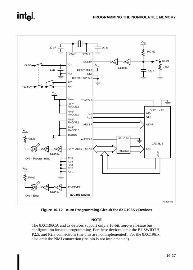
16-27
PROGRAMMING THE NONVOLATILE MEMORY
Figure 16-12. Auto Programming Circuit for 8 XC196Kx Devices
NOTE
The 8XC196CA and Jx devices support only a 16-bit, zero-wait-state bus configuration for auto programming. For these devices, omit the BUSWIDTH, P2.5, and P2.3 connections (the pins are not implemented). For the 8XC196Jx, also omit the NMI connection (the pin is not implemented).
270kΩ
+5.0V
XTAL1
20 pF20 pF
XTAL2
P2.7/PACT#
P2.5P2.4P2.3P2.2P2.1
P2.0/PVER
RESET#
+12.50V
100 kΩ
1 kΩ
10µF74HC14
1.0µF
Reset
EA#
VPP
VREF
P0.7/ PMODE.3
P0.6/ PMODE.2
P0.5/ PMODE.1
P0.4/ PMODE.0
ANGND
READY/P5.6
NMIBUSWIDTH/P5.7
RD#/P5.3
P1.2P1.1
AD13:8
87C196 Device
A7:0
ALE/P5.0
A13:8
A14
OE# CE#
LE OE#
O7:
0
A15
74LS373
VCC
VCC
VCC
A0296-03
VCC
VCC
VSS
27(C)512
270kΩ
VCC
74HC14
74HC14
ON = Programming
ON = Error
AD7:0

8XC196Kx, Jx, CA USER’S MANUAL
16-28
16.9.2 Operating Environment
In the auto programming mode, the PCCBs are loaded into the chip configuration registers. Sincethe device gets programming data through the external bus, the memory device in the program-ming system must correspond to the default configuration (Figure 16-6 on page 16-19). Auto pro-gramming requires an 8-bit bus configuration, so the circuit must tie the BUSWIDTH pin low.The PCCB defaults allow you to use any standard EPROM that satisfies the AC specificationslisted in the device datasheet.
The auto programming mode also loads CCB0 into an internal RAM location and checks the lockbits. If either lock bit is programmed, the auto programming routine compares the internal secu-rity key to the external security key location. If the verification fails, the device enters an endlessinternal loop. If the security keys match, the routine continues. The auto programming routineuses the modified quick-pulse algorithm and the pulse width value programmed into the externalEPROM (locations 14H and 15H).
16.9.3 Auto Programming Routine
Figure 16-13 illustrates the auto programming routine. This routine checks the security lock bitsin CCB0; if either bit is programmed, it compares the internal security key to the external securitykey locations. If the security keys match, the routine continues; otherwise, the device enters anendless loop.
Table 16-11. Auto Programming Memory Map
Address Output from
8XC196 Device (A15:0)
InternalOTPROMAddress
Address Using Circuit
in Figure 16-12
(P1.2:1, A13:0)
Description
4014H N/A 14H Programming pulse width (PPW) LSB.
4015H N/A 15H Programming pulse width (PPW) MSB.
4020–402FH 2020–202FH 0020–002FH Security key for verification.
4000–6FFFH 2000–4FFFH 4000–6FFFH Code, data, and reserved locations. (KQ, JQ)
4000–7FFFH 2000–5FFFH 4000–7FFFH Code, data, and reserved locations. (KR, JR)
4000–7FFFH 2000–7FFFH 4000–9FFFH Code, data, and reserved locations. (KS)
4000–7FFFH 2000–9FFFH 4000–BFFFH Code, data, and reserved locations. (KT, JT, CA)
A000–FFFEH8000–DFFEH
2000–7FFEH8000–DFFEH
2000–4FFFH5000–7FFFH
Code, data, and reserved locations. (JV)

16-29
PROGRAMMING THE NONVOLATILE MEMORY
Figure 16-13. Auto Programming Routine
NoOther Modes
Loop Forever
A0191-03
PMODE = 0CH ?
No Lock Bits Enabled
?
Load PPW
Yes
NoPass ?
Yes
Verify Security Key
Assert PACT#
Get External Data
No
YesData = 0FFFFH
?
Execute Modified Quick-Pulse Algorithm
then Return
YesTop of OTPROM
?
No Deassert PACT# Loop Forever
(Done)
Clear PVER
Error Programming
?
Yes
Increment Address Pointer
No
Yes

8XC196Kx, Jx, CA USER’S MANUAL
16-30
If the security key verification is successful, the routine loads the programming pulse width(PPW) value from the external EPROM into the internal PPW register. It then asserts PACT#, in-dicating that programming has begun. (PACT# is also active during reset, although no program-ming is in progress.) PVER is initially asserted and remains asserted unless an error is detected,in which case it is deasserted.
The routine then reads the contents of the external EPROM, beginning at 4000H. It skips anyword that contains FFFFH (unprogrammed state). When it reads a word that contains any valueother than FFFFH, the routine calls the modified quick-pulse algorithm, which writes that valueto the OTPROM, using the appropriate number of pulses for the device, then verifies the result.The routine repeats this activity until the entire OTPROM is programmed, then deasserts PACT#and enters an endless loop. It takes approximately 40 seconds to program 16 Kbytes of OTPROM.
16.9.4 Auto Programming Procedure
If a glitch or reset occurs while programming the security key and lock bits, an unknown securitykey might accidentally be written, rendering the device inaccessible for further programming. Tominimize this possibility, follow this recommended programming procedure.
NOTE
All addresses are given for the circuit shown in Figure 16-12 on page 16-27. If you choose a different circuit, you must adjust the addresses accordingly.
1. Using a blank EPROM device, follow these steps to skip programming of CCB0 andprogram the rest of the OTPROM array, including the security key.
— Place the programming pulse width (PPW) in external EPROM locations 14H–15H.
— Leave the external CCB0 location (4018H) unprogrammed (0FFFFH).
— Place the appropriate CCB1 value at external location 401AH.
— Place the security key to be programmed in external EPROM locations 4020H–402FH.
— Place the value 20H in external EPROM locations 4019H and 401BH (for the reservedOTPROM locations that require this value).
— Place the desired code in the remaining external EPROM locations 4000H and above(see Table 16-11 on page 16-28).
— Execute the power-up sequence (page 16-15) to initiate auto programming.
— When programming is complete, execute the powerdown sequence (page 16-15) beforecontinuing to step 2.

16-31
PROGRAMMING THE NONVOLATILE MEMORY
2. Using another blank EPROM device, follow these steps to program only CCB0.
— Place the programming pulse width (PPW) in external locations 14H–15H.
— Place the appropriate CCB0 value in external location 4018H.
— Place the security key to be verified in external EPROM locations 0020H–002FH. Thisvalue must match the security key programmed in step 1.
— Leave the remaining EPROM locations unprogrammed (0FFFFH).
— Execute the power-up sequence (page 16-15) to initiate auto programming.
— When programming is complete, follow the powerdown sequence (page 16-15).
At this point, you can modify the circuit, then use ROM-dump mode to write the entire OTPROMarray to an external memory device and verify its contents. (See “ROM-dump Mode” for details.)
16.9.5 ROM-dump Mode
The ROM-dump mode provides an easy way to verify the contents of the OTPROM array afterauto programming. Use the same circuit as for auto programming, but change the connections ofthe PMODE (P0.7:4) pins. To select ROM-dump mode (PMODE=6H), connect P0.6 and P0.5 toVCC and connect P0.7 and P0.4 to ground. The same bank switching mechanism is used and thememory map is the same as that for auto programming. The example circuit (Figure 16-12 onpage 16-27) does not show the necessary WR# and VPP connections to allow writing to theEPROM. And although the example uses an EPROM, you could also use a RAM device. Alter-natively, you could dump the OTPROM contents to any 16-bit parallel port.
For the 8XC196JV, which has 48 Kbytes of OTPROM, use a word-wide memory device or a 16-bit parallel port for the ROM dump. The internal algorithm dumps the first 24 Kbytes ofOTPROM (2000–7FFFH) to the 12 Kwords at 2000–4FFFH and the remaining 24 Kbytes (8000–DFFFH) to the 12 Kwords at external locations 5000–7FFFH.
NOTE
If you have programmed the DED bit (USFR.2), ROM-dump mode is disabled. (See “Controlling Fetches from External Memory” on page 16-6).
To enter ROM-dump mode, follow the power-up sequence on page 16-15. The ROM-dump modechecks the security key regardless of the CCR security-lock bits. If you have programmed a se-curity key, a matching key must reside in the external memory; otherwise, the device enters anendless loop. If the security key verifies, ROM-dump mode fetches the PPW, then writes the en-tire OTPROM array to external memory. PACT# remains low while the dump is in progress, thengoes high to indicate that the dump is complete.
8XC196Kx, Jx, CA USER’S MANUAL
16-32
16.10 SERIAL PORT PROGRAMMING MODE
The serial port programming mode enables the serial I/O (SIO) port to write data to the OTPROMthrough the TXD (P2.0) pin and read it through the RXD (P2.1) pin. In this mode, the device ex-ecutes a program from its internal test ROM. This program is a modified version of the reducedinstruction set monitor (RISM) that exists on all 8X9X evaluation boards. The simple hardwaresetup of this mode makes it useful for in-module testing, programming, and in-line diagnostics.Special software, called IBSP196, simplifies communication between the device and a smart ter-minal. This software is available free of charge through the Intel BBS. (See “Bulletin Board Sys-tem (BBS)” on page 1-9.)
NOTE
Serial port programming mode has no provision for security-key verification. If a security key has been programmed, an attempt to enter serial port programming mode causes the device to enter an endless loop.
Entering serial port programming mode with VPP at +12.5 volts allows you to modify code inOTPROM or to program small segments of OTPROM to customize code for a particular module.(Programming more than 2 Kbytes of OTPROM is not recommended in this mode because of itsrelatively long programming time.)
Entering serial port programming mode with VPP at +5.0 volts enables you to perform these func-tions:
• download a module-testing program into internal RAM and execute it without alteringnonvolatile memory or using dedicated OTPROM software space
• run a segment of code in OTPROM and monitor its performance during execution
• examine the code programmed into the OTPROM
• examine the contents of any register
• manipulate RAM, SFRs, or pin states
16.10.1 Serial Port Programming Circuit and Memory Map
Figure 16-14 shows the recommended circuit for serial port programming. In this mode, data istransmitted and received through the TXD (P2.0) and RXD (P2.1) pins. Connect these pins to anysmart terminal capable of communicating with the RISM. Any host that requires an RS-232C in-terface (such as a PC) must be connected through an RS-232C driver/receiver such as the oneshown within the dashed line in Figure 16-14. XTAL1 and XTAL2 can be connected to a crystalwith a frequency between 3.5 MHz and 16 MHz. The frequency must correspond to the value inthe SP_BAUD register (see “Changing Serial Port Programming Defaults” on page 16-34).

16-33
PROGRAMMING THE NONVOLATILE MEMORY
Figure 16-14. Serial Port Programming Mode Circuit
5 9 4 8 3 7 2 6 1
1.8kΩ
1.8kΩ
1.8kΩ
1.8kΩ 1.8kΩ10µF
A0298-04
RXD
TXD
RXD
TXD
VCC
87C196 Device
30 pF30 pF
XTAL1 XTAL2
P0.7/PMODE.3
P0.6/PMODE.2
P0.5/PMODE.1
P0.4/PMODE.0
ANGND
VREF
VCC
A B C
VCC
VPP
EA#
0.01 µF
VPP
P2.0/TXD
P2.1/RXD
10 µF
VCC
RESET#
NMI
READY/P5.6
BUSWIDTH/5.7
1N914
2N2222A
2N2907
1N914

8XC196Kx, Jx, CA USER’S MANUAL
16-34
Because the RISM begins at location 2000H in serial port programming mode, the OTPROM lo-cations are automatically remapped as shown in Table 16-12. For example, to access OTPROMlocation 2000H in serial port programming mode, you must address it as A000H.
16.10.2 Changing Serial Port Programming Defaults
Several locations in test ROM are used to control operating parameters. The test ROM routineestablishes the default values shown in Table 16-13. To change the default values, write the de-sired values to the test ROM addresses shown in the table. (Refer to the SP_BAUD, SP_CON,and SP_PPW register descriptions in Appendix C.) After you write the new values to the testROM locations, the RISM writes the programmed values into the associated registers.
The default programming pulse width is longer than required. To avoid unnecessarily long pro-gramming times, change the default value before beginning to program the device. For a 100-µspulse width, use the following formula to determine the required PPW_VALUE and write thatvalue to the test ROM location listed in Table 16-13.
Table 16-12. Serial Port Programming Mode Memory Map
Description Device
Address Range (Hex)
Normal Operation
Serial Port Programming Mode
Internal OTPROM
87C196JV 2000–DFFF A000–FFFF, 8000–DFFF†
87C196CA, JT, KT 2000–9FFF A000–FFFF, 8000–9FFF††
87C196KS 2000–7FFF A000–FFFF
87C196JR, KR 2000–5FFF A000–DFFF
87C196JQ, KQ 2000–4FFF A000–CFFF
External memory87C196CA, JT, KT, JV — 4000–7FFF
87C196JQ, KQ, JR, KR, KS — 4000–9FFF
Do not address All — 2400–3FFF
Test ROM and RISM All — 2000–23FF
†For the 87C196JV, the lower 24 Kbytes of internal OTPROM (2000–7FFFH) are remapped to A000–FFFFH. The upper 24 Kbytes must be addressed as 8000–DFFFH. A bank switching mechanism differen-tiates between the two address ranges. To program the upper 24 Kbytes of the internal OTPROM, execute this instruction: orb tmr, #80h.††For the 87C196CA, JT, and KT, the lower 24 Kbytes of internal OTPROM (2000–7FFFH) are remapped to A000–FFFFH. The upper 8 Kbytes must be addressed as 8000–9FFFH.
PPW_VALUE 0.6944 Fosc×( ) 1–=
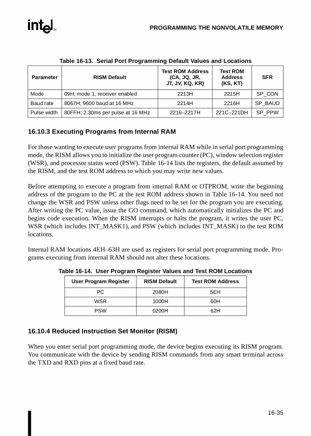
16-35
PROGRAMMING THE NONVOLATILE MEMORY
16.10.3 Executing Programs from Internal RAM
For those wanting to execute user programs from internal RAM while in serial port programmingmode, the RISM allows you to initialize the user program counter (PC), window selection register(WSR), and processor status word (PSW). Table 16-14 lists the registers, the default assumed bythe RISM, and the test ROM address to which you may write new values.
Before attempting to execute a program from internal RAM or OTPROM, write the beginningaddress of the program to the PC at the test ROM address shown in Table 16-14. You need notchange the WSR and PSW unless other flags need to be set for the program you are executing.After writing the PC value, issue the GO command, which automatically initializes the PC andbegins code execution. When the RISM interrupts or halts the program, it writes the user PC,WSR (which includes INT_MASK1), and PSW (which includes INT_MASK) to the test ROMlocations.
Internal RAM locations 4EH–63H are used as registers for serial port programming mode. Pro-grams executing from internal RAM should not alter these locations.
16.10.4 Reduced Instruction Set Monitor (RISM)
When you enter serial port programming mode, the device begins executing its RISM program.You communicate with the device by sending RISM commands from any smart terminal acrossthe TXD and RXD pins at a fixed baud rate.
Table 16-13. Serial Port Programming Default Values and Locations
Parameter RISM DefaultTest ROM Address
(CA, JQ, JR, JT, JV, KQ, KR)
Test ROM Address(KS, KT)
SFR
Mode 09H; mode 1, receiver enabled 2213H 2215H SP_CON
Baud rate 8067H; 9600 baud at 16 MHz 2214H 2216H SP_BAUD
Pulse width 80FFH; 2.30ms per pulse at 16 MHz 2216–2217H 221C–221DH SP_PPW
Table 16-14. User Program Register Values and Test ROM Locations
User Program Register RISM Default Test ROM Address
PC 2080H 5EH
WSR 1000H 60H
PSW 0200H 62H

8XC196Kx, Jx, CA USER’S MANUAL
16-36
Upon entering serial port programming mode, the device enters a waiting loop, calledMonitor_Pause, in which it waits for RISM commands to arrive across the serial port. The com-mands are each one byte in length and have values between 00H and 1FH. A value between 00Hand 1FH is considered a command unless it follows a data latch enable (SET_DLE_FLAG) com-mand. The SET_DLE_FLAG command sets the DLE flag in the MODE register (57H). The DLEflag alerts the RISM to store the next byte in the DATA register, a 32-bit first-in-last-out (FILO)register located at 58H.
When a receive interrupt occurs, the RISM checks the data value and the DLE flag. If the datavalue is greater than 1FH or if the DLE flag is set, the received byte is considered data and isstored in the DATA register (58H). Each time new data is received, the DATA register is shiftedleft by eight bits. If the value is between 00H and 1FH and the DLE flag is clear, the received byteis considered a command. Commands are stored in the CHAR register (56H). After it executeseach command, the RISM resumes Monitor_Pause, except where otherwise noted.
To access a particular address, you must first send the address across the serial port as data. Sendit one byte at a time, with the high byte first (the address is always assumed to be 16 bits). TheRISM stores the address data in the DATA register. Now you must transfer the address from theDATA register to the ADDR register (5CH) by sending the DATA_TO_ADDR command (0AH).
16.10.5 RISM Command Descriptions
Table 16-15 lists and describes the RISM commands. The following sections provide examples.
Table 16-15. RISM Command Descriptions
Value Command Description
00H SET_DLE_FLAG Sets the DLE flag in bit 0 of the MODE register (57H) to tell the RISM that the next byte on the serial port is data that should be loaded into the DATA register (58H). The flag is cleared as soon as the byte is read.
02H TRANSMIT Transmits the low byte of the DATA register to the serial port through the CHAR register, shifts the DATA register right (long) by eight bits, and increments ADDR by one.
ADDR DATA SBUF_TX
Before command 22 14 7A 2F 80 67
After command 22 15 00 7A 2F 80 67

16-37
PROGRAMMING THE NONVOLATILE MEMORY
04H READ_BYTE Puts the contents of the (byte) memory address pointed to by the ADDR register into the low byte of the DATA register.
Memory Addr.
ADDR DATA 2215 2214
Before command 22 14 80 67
After command 22 14 67 80 67
05H READ_WORD Puts the contents of the (word) memory address pointed to by the ADDR register into the low byte of the DATA register.
Memory Addr.
ADDR DATA 2215 2214
Before command 22 14 80 67
After command 22 14 80 67 80 67
07H WRITE_BYTE Puts the low byte of the DATA register into the memory address pointed to by the ADDR register and increments ADDR by one.
Memory Addr.
ADDR DATA 2217 2216
Before command 22 16 2E 11 80 09 FF FF
After command 22 17 2E 11 80 09 FF 09
NOTE: To write to an OTPROM location, VPP must be at +12.5 volts. To write toan internal RAM location, VPP can be at either +5.0 volts or +12.5 volts.
08H WRITE_WORD Puts the low word of the DATA register into the memory address pointed to by the ADDR register and increments ADDR by two.
Memory Addr.
ADDR DATA 2217 2216
Before command 22 16 2E 11 80 09 FF FF
After command 22 18 2E 11 80 09 80 09
NOTE
To write to an OTPROM location, VPP must be at +12.5 volts. To write to an internal RAM location, VPP can be at either +5.0 volts or +12.5 volts.
Table 16-15. RISM Com mand Descriptions (Continued)
Value Command Description

8XC196Kx, Jx, CA USER’S MANUAL
16-38
16.10.6 RISM Command Examples
This section provides examples of ways in which you might use the RISM commands.
0AH DATA_TO_ADDR Puts the low word of the DATA register into the ADDR register.
ADDR DATA
Before command F1 05 22 16
After command 22 16 F1 05 22 16
0BH INDIRECT Puts the word from the memory address pointed to by the ADDR register into the ADDR register.
Memory Addr.
ADDR 2217 2216
Before command 22 16 80 09
After command 80 09 80 09
12H GO PUSHes the user PC, PSW, and WSR onto the stack and starts your program from the location contained in the user PC. The RISM PC, PSW, and WSR will also be in the stack, so allow enough room on the stack for all six words. Your program must not directly alter memory locations 56H–5CH; the RISM uses these locations if your program reads from or writes to any memory.
You can interrogate memory locations while your program is running. The RISM interrupts your program to process the command, then returns execution to your program.
13H HALT Stops executing your program, POPs the user PC, PSW, and WSR from the stack, and PUSHes the RISM PC, PSW, and WSR back onto the stack. The RISM PC contains the location of the Monitor_Pause routine, so the RISM returns to Monitor_Pause.
14H REPORT Loads a value into the DATA register. This value indicates the status of your program:
Value Status
00 halted01 running02 trapped
Table 16-15. RISM Com mand Descriptions (Continued)
Value Command Description

16-39
PROGRAMMING THE NONVOLATILE MEMORY
16.10.6.1 Example 1 — Programming the PPW
You should specify the programming pulse width before you do any programming or write to anymemory locations. This example assumes an 87C196KT device. It loads the SP_PPW register(221CH/221DH) with 8010H, the minimum value for 16-MHz operation. (See “ProgrammingPulse Width” on page 16-8 to determine the correct PPW for other frequencies.)
Before this programming step takes place, the SP_PPW register contains its default value,80FFH. The PPW is equal to 2.30 ms, so this program step will take 11.52 ms per word to com-plete (5 pulses of 2.30ms each). After the PPW value is changed, subsequent programming oper-ations will take only 500 µs per word (5 pulses of 100 µs each).
Because an OTPROM location is being altered, VPP must be at +12.5 volts. RISM commandsmust be sent across the serial port one byte at a time, and a SET_DLE_FLAG command mustprecede any data byte that is less than 1FH. The address being modified must first be loaded intothe DATA register, then transferred to the ADDR register.
Any write operation can be done in this manner.
Send Comments (Example 1) DATA ADDR
22 Data. High byte of address to DATA register. 22
00 SET_DLE_FLAG. The next data byte is < 1FH. 22
1C Data. Low byte of address to DATA register. 22 1C
0A DATA_TO_ADDR. Move address to ADDR. 22 1C 22 1C
80 Data. High byte of data to DATA register. 22 1C 80 22 1C
00 SET_DLE_FLAG. The next data byte is < 1FH. 22 1C 80 22 1C
10 Data. Low byte of data to DATA register. 22 1C 80 10 22 1C
08 WRITE_WORD. Low word of DATA to memory location 221C (contents of ADDR). Increment ADDR by two.
22 1C 80 10 22 1C
Memory Addresses
221D 221C
80 10 22 1E

8XC196Kx, Jx, CA USER’S MANUAL
16-40
16.10.6.2 Example 2 — Reading OTPROM Contents
This example reads the contents of OTPROM address A080H. Because the OTPROM isremapped from 2000H to A000H, the location read is actually 2080H of the program inOTPROM. This example assumes that the word at location 2080H is 8067H, the assembled hexvalue of the code. No OTPROM locations are changed, so VPP can be either +12.5 volts or +5volts.
Any address can be read in this manner, including register RAM, internal RAM, and SFRs.
16.10.6.3 Example 3 — Loading a Program into Internal RAM
This example loads a program into internal RAM. No OTPROM locations are changed, so VPP
can be either +12.5 volts or +5 volts. The following program is to be loaded:
400 A1221180 LD 80H, #1122H ;Puts 1122H into register RAM location 80H404 27FE SJMP 0404H ;Jumps to itself to keep program running
;indefinitely
The hex file must be loaded one byte at a time using the RISM commands.
Send Comments (Example 2) DATA ADDR
A0 Data. High byte of address to DATA register. A0
80 Data. Low byte of address to DATA register. A0 80
0A DATA_TO_ADDR. Move address to DATA register. A0 80 A0 80
05 READ_WORD. Put word at A080H into DATA. A0 80 80 67 A0 80
02 TRANSMIT. Transmit low byte of DATA across the serial port, increment ADDR by one, and shift DATA right long by eight bits.
00 A0 80 80 A0 81
02 TRANSMIT. Transmit low byte of DATA across the serial port, increment ADDR by one, and shift DATA right long by eight bits.
00 00 A0 80 A0 82
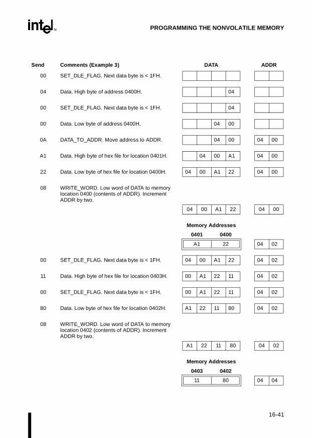
16-41
PROGRAMMING THE NONVOLATILE MEMORY
Send Comments (Example 3) DATA ADDR
00 SET_DLE_FLAG. Next data byte is < 1FH.
04 Data. High byte of address 0400H. 04
00 SET_DLE_FLAG. Next data byte is < 1FH. 04
00 Data. Low byte of address 0400H. 04 00
0A DATA_TO_ADDR. Move address to ADDR. 04 00 04 00
A1 Data. High byte of hex file for location 0401H. 04 00 A1 04 00
22 Data. Low byte of hex file for location 0400H. 04 00 A1 22 04 00
08 WRITE_WORD. Low word of DATA to memory location 0400 (contents of ADDR). Increment ADDR by two.
04 00 A1 22 04 00
Memory Addresses
0401 0400
A1 22 04 02
00 SET_DLE_FLAG. Next data byte is < 1FH. 04 00 A1 22 04 02
11 Data. High byte of hex file for location 0403H. 00 A1 22 11 04 02
00 SET_DLE_FLAG. Next data byte is < 1FH. 00 A1 22 11 04 02
80 Data. Low byte of hex file for location 0402H. A1 22 11 80 04 02
08 WRITE_WORD. Low word of DATA to memory location 0402 (contents of ADDR). Increment ADDR by two.
A1 22 11 80 04 02
Memory Addresses
0403 0402
11 80 04 04

8XC196Kx, Jx, CA USER’S MANUAL
16-42
16.10.6.4 Example 4 — Setting the PC and Executing the Program
This example sets the PC and begins executing the program loaded in example 3. The PC (at lo-cation 5EH) must be set at 400H to tell the RISM where to begin execution of the program. TheWSR and PSW are automatically set to their default values (1000H and 200H, respectively), butcan be changed in this same manner. No OTPROM locations are changed, so VPP can be either+12.5 volts or +5 volts. .
27 Data. High byte of hex file for location 0405H. 22 11 80 27 04 04
FE Data. Low byte of hex file for location 0404H. 11 80 27 FE 04 04
08 WRITE_WORD. Low word of DATA to memory location 0404 (contents of ADDR). Increment ADDR by two.
11 80 27 FE 04 04
Memory Addresses
0405 0404
27 FE 04 06
Send Comments (Example 4) DATA ADDR
00 SET_DLE_FLAG. Next data byte is < 1FH.
00 Data. High byte of PC address 005EH. 00
5E Data. Low byte of PC address 005EH. 00 5E
0A DATA_TO_ADDR. Move address to ADDR. 00 5E 00 5E
00 SET_DLE_FLAG. Next data byte is < 1FH. 00 5E 00 5E
04 Data. High byte of program address 0400H. 00 5E 04 00 5E
00 SET_DLE_FLAG. Next data byte is < 1FH. 00 5E 04 00 5E
00 Data. Low byte of program address 0400H. 00 5E 04 00 00 5E
Send Comments (Example 3) DATA ADDR
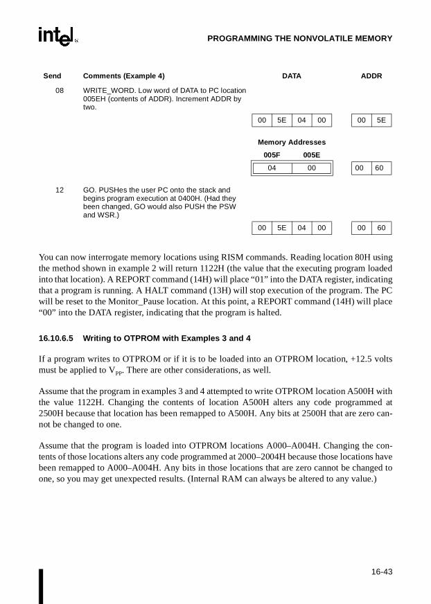
16-43
PROGRAMMING THE NONVOLATILE MEMORY
You can now interrogate memory locations using RISM commands. Reading location 80H usingthe method shown in example 2 will return 1122H (the value that the executing program loadedinto that location). A REPORT command (14H) will place “01” into the DATA register, indicatingthat a program is running. A HALT command (13H) will stop execution of the program. The PCwill be reset to the Monitor_Pause location. At this point, a REPORT command (14H) will place“00” into the DATA register, indicating that the program is halted.
16.10.6.5 Writing to OTPROM with Examples 3 and 4
If a program writes to OTPROM or if it is to be loaded into an OTPROM location, +12.5 voltsmust be applied to VPP. There are other considerations, as well.
Assume that the program in examples 3 and 4 attempted to write OTPROM location A500H withthe value 1122H. Changing the contents of location A500H alters any code programmed at2500H because that location has been remapped to A500H. Any bits at 2500H that are zero can-not be changed to one.
Assume that the program is loaded into OTPROM locations A000–A004H. Changing the con-tents of those locations alters any code programmed at 2000–2004H because those locations havebeen remapped to A000–A004H. Any bits in those locations that are zero cannot be changed toone, so you may get unexpected results. (Internal RAM can always be altered to any value.)
08 WRITE_WORD. Low word of DATA to PC location 005EH (contents of ADDR). Increment ADDR by two.
00 5E 04 00 00 5E
Memory Addresses
005F 005E
04 00 00 60
12 GO. PUSHes the user PC onto the stack and begins program execution at 0400H. (Had they been changed, GO would also PUSH the PSW and WSR.)
00 5E 04 00 00 60
Send Comments (Example 4) DATA ADDR

8XC196Kx, Jx, CA USER’S MANUAL
16-44
16.11 RUN-TIME PROGRAMMING
You can program an OTPROM location during normal code execution. To make the OTPROMarray accessible, apply VCC voltage to EA# while you reset the device. Apply VPP voltage to theVPP pin during the entire programming process. Then simply write to the location to be pro-grammed.
NOTE
Programming either security-lock bit in CCB0 disables run-time programming. (For details, see “Controlling Access to the OTPROM During Normal Operation” on page 16-4.)
Immediately after writing to the OTPROM, the device must either enter idle mode or execute codefrom external memory. An access to OTPROM would abort the current programming cycle. Eachprogramming cycle begins when a word is written to the OTPROM and ends when the nextOTPROM access occurs. Each word requires a total of five programming cycles, each of whichmust be approximately 100 µs in duration.
Figure 16-15 is a run-time programming example. It performs five programming cycles for eachword. After each programming cycle, the code causes the device to enter idle mode. EPA0 causesthe device to exit idle mode at the appropriate time. To ensure that the device does not exit idlemode prematurely, all other interrupts are disabled.
The routine assumes that the following conditions are true:
• the EPA is dedicated to run-time programming
• timer 1 is configured to use an internal clock
• EPA0_ISR is assigned as the EPA0 interrupt vector.
It also assumes that the following constants and registers are assigned:
CLEAR_EPA0 constant (0EFH) that clears the EPA0 interrupt pending bit
ENABLE_EPA0 constant (10H) that enables only the EPA0 interrupt
EPA0_TIMER constant (40H) that sets up EPA0 as a software timer using timer 1
PGM_PULSE constant that determines programming pulse width
ADDR_TEMP register that contains the address to be programmed
COUNT count register
DATA_TEMP register that contains the data to be programmed
TEMP0 temporary register
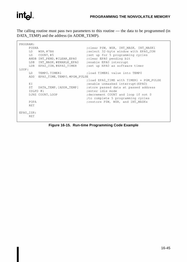
16-45
PROGRAMMING THE NONVOLATILE MEMORY
The calling routine must pass two parameters to this routine — the data to be programmed (inDATA_TEMP) and the address (in ADDR_TEMP).
Figure 16-15. Run-time Programming Code Example
PROGRAM:PUSHA ;clear PSW, WSR, INT_MASK, INT_MASK1LD WSR,#7BH ;select 32-byte window with EPA0_CONLD COUNT,#5 ;set up for 5 programming cyclesANDB INT_PEND,#CLEAR_EPA0 ;clear EPA0 pending bitLDB INT_MASK,#ENABLE_EPA0 ;enable EPA0 interruptLDB EPA0_CON,#EPA0_TIMER ;set up EPA0 as software timer
LOOP:LD TEMP0,TIMER1 ;load TIMER1 value into TEMP0ADD EPA0_TIME,TEMP0,#PGM_PULSE
;load EPA0_TIME with TIMER1 + PGM_PULSEEI ;enable unmasked interrupt(EPA0)ST DATA_TEMP,[ADDR_TEMP] ;store passed data at passed addressIDLPD #1 ;enter idle modeDJNZ COUNT,LOOP ;decrement COUNT and loop if not 0
;to complete 5 programming cyclesPOPA ;restore PSW, WSR, and INT_MASKsRET
EPA0_ISR:RET

AInstruction Set Reference


A-1
APPENDIX AINSTRUCTION SET REFERENCE
This appendix provides reference information for the instruction set of the family of MCS® 96microcontrollers. It defines the processor status word (PSW) flags, describes each instruction,shows the relationships between instructions and processor status word (PSW) flags, and showshexadecimal opcodes, instruction lengths, and execution times. It includes the following tables.
• Table A-1 on page A-2 is a map of the opcodes.
• Table A-2 on page A-4 defines the processor status word (PSW) flags.
• Table A-3 on page A-5 shows the effect of the PSW flags or a specified register bit onconditional jump instructions.
• Table A-4 on page A-5 defines the symbols used in Table A-6.
• Table A-5 on page A-6 defines the variables used in Table A-6 to represent instructionoperands.
• Table A-6 on page A-7 lists the instructions alphabetically, describes each of them, andshows the effect of each instruction on the PSW flags.
• Table A-7 beginning on page A-42 lists the instruction opcodes, in hexadecimal order,along with the corresponding instruction mnemonics.
• Table A-8 on page A-48 lists instruction lengths and opcodes for each applicable addressingmode.
• Table A-9 on page A-54 lists instruction execution times, expressed in state times.
NOTE
The # symbol prefixes an immediate value in immediate addressing mode. Chapter 3, “Programming ConsiderAtions,” describes the operand types and addressing modes.
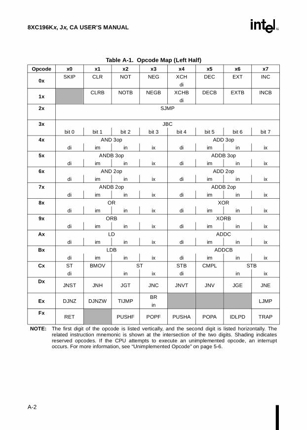
8XC196Kx, Jx, CA USER’S MANUAL
A-2
Table A-1. Opcode Map (Left Half)Opcode x0 x1 x2 x3 x4 x5 x6 x7
0xSKIP CLR NOT NEG XCH
di
DEC EXT INC
1xCLRB NOTB NEGB XCHB
di
DECB EXTB INCB
2x SJMP
3x JBC
bit 0 bit 1 bit 2 bit 3 bit 4 bit 5 bit 6 bit 7
4x AND 3op ADD 3op
di im in ix di im in ix
5x ANDB 3op ADDB 3op
di im in ix di im in ix
6x AND 2op ADD 2op
di im in ix di im in ix
7x ANDB 2op ADDB 2op
di im in ix di im in ix
8x OR XOR
di im in ix di im in ix
9x ORB XORB
di im in ix di im in ix
Ax LD ADDC
di im in ix di im in ix
Bx LDB ADDCB
di im in ix di im in ix
Cx ST BMOV ST STB CMPL STB
di in ix di in ix
DxJNST JNH JGT JNC JNVT JNV JGE JNE
Ex DJNZ DJNZW TIJMPBR
inLJMP
FxRET PUSHF POPF PUSHA POPA IDLPD TRAP
NOTE: The first digit of the opcode is listed vertically, and the second digit is listed horizontally. Therelated instruction mnemonic is shown at the intersection of the two digits. Shading indicatesreserved opcodes. If the CPU attempts to execute an unimplemented opcode, an interruptoccurs. For more information, see “Unimplemented Opcode” on page 5-6.

A-3
INSTRUCTION SET REFERENCE
Table A-1. Opcode Map (Right Half)
Opcode x8 x9 xA xB xC xD xE xF
0xSHR SHL SHRA XCH
ix
SHRL SHLL SHRAL NORML
1xSHRB SHLB SHRAB XCHB
ix
(Note 1) (Note 1) (Note 1) (Note 1)
2x SCALL
3x JBS
bit 0 bit 1 bit 2 bit 3 bit 4 bit 5 bit 6 bit 7
4x SUB 3op MULU 3op (Note 2)
di im in ix di im in ix
5x SUBB 3op MULUB 3op (Note 2)
di im in ix di im in ix
6x SUB 2op MULU 2op (Note 2)
di im in ix di im in ix
7x SUBB 2op MULUB 2op (Note 2)
di im in ix di im in ix
8x CMP DIVU (Note 2)
di im in ix di im in ix
9x CMPB DIVUB (Note 2)
di im in ix di im in ix
Ax SUBC LDBZE
di im in ix di im in ix
Bx SUBCB LDBSE
di im in ix di im in ix
Cx PUSH POP BMOVI POP
di im in ix di in ix
DxJST JH JLE JC JVT JV JLT JE
Ex (Note 1) (Note 1) (Note 1) (Note 1) DPTS (Note 1) (Note 1) LCALL
FxCLRC SETC DI EI CLRVT NOP signed
MUL/DIV(Note 2)
RST
NOTES:1. For the 8XC196KS and KT only, this opcode is reserved, but it does not generate an unimplemented
opcode interrupt.2. Signed multiplication and division are two-byte instructions. The first byte is “FE” and the second is the
opcode of the corresponding unsigned instruction.

8XC196Kx, Jx, CA USER’S MANUAL
A-4
Table A-2. Processor Status Word (PSW) Flags
Mnemonic Description
C The carry flag is set to indicate an arithmetic carry from the MSB of the ALU or the state of the last bit shifted out of an operand. If a subtraction operation generates a borrow, the carry flag is cleared.
C Value of Bits Shifted Off
0 < ½ LSB
1 ≥ ½ LSB
Normally, the result is rounded up if the carry flag is set. The sticky bit flag allows a finer resolution in the rounding decision.
C ST Value of Bits Shifted Off
0 0 = 0
0 1 > 0 and < ½ LSB
1 0 = ½ LSB
1 1 > ½ LSB and < 1 LSB
N The negative flag is set to indicate that an operation generated a negative result. It is correct even if an overflow occurs. For all shift operations and the NORML instruction, the flag is set or cleared to equal the most-significant bit of the result, even if the shift count is zero.
ST The sticky bit flag is set to indicate that, during a right shift, a “1” has been shifted into the carry flag and then shifted out. This bit is undefined after a multiply operation. The sticky bit flag can be used with the carry flag to allow finer resolution in rounding decisions. See the description of the carry (C) flag for details.
V The overflow flag is set to indicate that the result of an operation is too large to be represented correctly in the available space.
For shift operations, the flag is set if the most-significant bit of the operand changes during the shift.
For divide operations, the quotient is stored in the low-order half of the destination operand and the remainder is stored in the high-order half. The overflow flag is set if the quotient is outside the range for the low-order half of the destination operand. (Chapter 3, “Programming ConsiderAtions,” defines the operands and possible values for each.)
Instruction Quotient Stored in: V Flag Set if Quotient is:
DIVB Short-Integer < –128 (81H) or > +127 (7FH)
DIV Integer < –32768 (8001H) or > +32767 (7FFFH)
DIVUB Byte > 255 (0FFH)
DIVU Word > 65535 (0FFFFH)
VT The overflow-trap flag is set when the overflow flag is set, but it is cleared only by the CLRVT, JVT, and JNVT instructions. This allows testing for a possible overflow at the end of a sequence of related arithmetic operations, which is generally more efficient than testing the overflow flag after each operation.
Z The zero flag is set to indicate that the result of an operation was zero. For add-with-carry and subtract-with-borrow operations, the flag is never set, but it is cleared if the result is other than zero. Therefore, the zero flag indicates the correct zero or non-zero result for multiple-precision calculations.
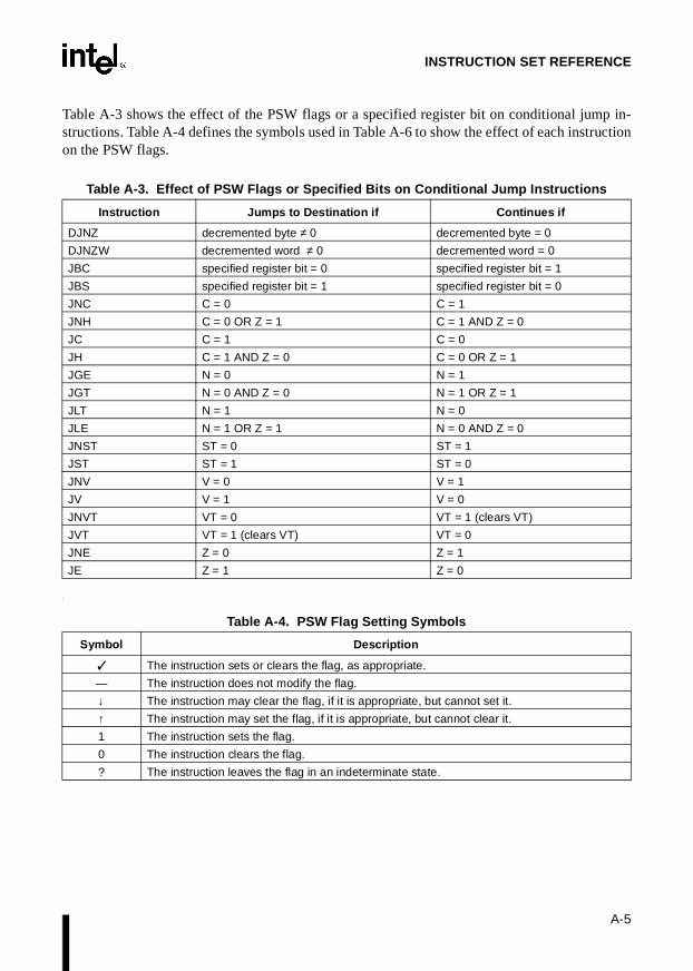
A-5
INSTRUCTION SET REFERENCE
Table A-3 shows the effect of the PSW flags or a specified register bit on conditional jump in-structions. Table A-4 defines the symbols used in Table A-6 to show the effect of each instructionon the PSW flags.
.
Table A-3. Effect of PSW Flags or Specified Bits on Conditional Jump Instructions
Instruction Jumps to Destination if Continues if
DJNZ decremented byte ≠ 0 decremented byte = 0
DJNZW decremented word ≠ 0 decremented word = 0
JBC specified register bit = 0 specified register bit = 1
JBS specified register bit = 1 specified register bit = 0
JNC C = 0 C = 1
JNH C = 0 OR Z = 1 C = 1 AND Z = 0
JC C = 1 C = 0
JH C = 1 AND Z = 0 C = 0 OR Z = 1
JGE N = 0 N = 1
JGT N = 0 AND Z = 0 N = 1 OR Z = 1
JLT N = 1 N = 0
JLE N = 1 OR Z = 1 N = 0 AND Z = 0
JNST ST = 0 ST = 1
JST ST = 1 ST = 0
JNV V = 0 V = 1
JV V = 1 V = 0
JNVT VT = 0 VT = 1 (clears VT)
JVT VT = 1 (clears VT) VT = 0
JNE Z = 0 Z = 1
JE Z = 1 Z = 0
Table A-4. PSW Flag Setting Symbols
Symbol Description
The instruction sets or clears the flag, as appropriate.
— The instruction does not modify the flag.
↓ The instruction may clear the flag, if it is appropriate, but cannot set it.
↑ The instruction may set the flag, if it is appropriate, but cannot clear it.
1 The instruction sets the flag.
0 The instruction clears the flag.
? The instruction leaves the flag in an indeterminate state.

8XC196Kx, Jx, CA USER’S MANUAL
A-6
Table A-5 defines the variables that are used in Table A-6 to represent the instruction operands.
Table A-5. Operand Variables
Variable Description
aa A 2-bit field within an opcode that selects the basic addressing mode used. This field is present only in those opcodes that allow addressing mode options. The field is encoded as follows:
00 register-direct 01 immediate 10 indirect 11 indexed
baop A byte operand that is addressed by any addressing mode.
bbb A 3-bit field within an opcode that selects a specific bit within a register.
bitno A 3-bit field within an opcode that selects one of the eight bits in a byte.
breg A byte register in the internal register file. When it could be unclear whether this variable refers to a source or a destination register, it is prefixed with an S or a D. The value must be in the range of 00–FFH.
cadd An address in the program code.
Dbreg† A byte register in the lower register file that serves as the destination of the instruction operation.
disp Displacement. The distance between the end of an instruction and the target label.
Dlreg† A 32-bit register in the lower register file that serves as the destination of the instruction operation. Must be aligned on an address that is evenly divisible by 4. The value must be in the range of 00–FCH.
Dwreg† A word register in the lower register file that serves as the destination of the instruction operation. Must be aligned on an address that is evenly divisible by 2. The value must be in the range of 00–FEH.
lreg A 32-bit register in the lower register file. Must be aligned on an address that is evenly divisible by 4. The value must be in the range of 00–FCH.
preg A pointer register. Must be aligned on an address that is evenly divisible by 4. The value must be in the range of 00–FCH.
Sbreg† A byte register in the lower register file that serves as the source of the instruction operation.
Slreg† A 32-bit register in the lower register file that serves as the source of the instruction operation. Must be aligned on an address that is evenly divisible by 4. The value must be in the range of 00–FCH.
Swreg† A word register in the lower register file that serves as the source of the instruction operation. Must be aligned on an address that is evenly divisible by 2. The value must be in the range of 00–FEH.
waop A word operand that is addressed by any addressing mode.
w2_reg A double-word register in the lower register file. Must be aligned on an address that is evenly divisible by 4. The value must be in the range of 00–FCH. Although w2_reg is similar to lreg, there is a distinction: w2_reg consists of two halves, each containing a 16-bit address; lreg is indivisible and contains a 32-bit number.
wreg A word register in the lower register file. When it could be unclear whether this variable refers to a source or a destination register, it is prefixed with an S or a D. Must be aligned on an address that is evenly divisible by 2. The value must be in the range of 00–FEH.
xxx The three high-order bits of displacement.†The D or S prefix is used only when it could be unclear whether a variable refers to a destination or a source register.

A-7
INSTRUCTION SET REFERENCE
Table A-6. Instruction Set
Mnemonic Operation Instruction Format
ADD(2 operands)
ADD WORDS. Adds the source and destination word operands and stores the sum into the destination operand.
(DEST) ← (DEST) + (SRC)
DEST, SRC
ADD wreg, waop
(011001aa) (waop) (wreg)
PSW Flag Settings
Z N C V VT ST
↑ —
ADD(3 operands)
ADD WORDS. Adds the two source word operands and stores the sum into the destination operand.
(DEST) ← (SRC1) + (SRC2)
DEST, SRC1, SRC2
ADD Dwreg, Swreg, waop
(010001aa) (waop) (Swreg) (Dwreg)
PSW Flag Settings
Z N C V VT ST
↑ —
ADDB(2 operands)
ADD BYTES. Adds the source and destination byte operands and stores the sum into the destination operand.
(DEST) ← (DEST) + (SRC)
DEST, SRC
ADDB breg, baop
(011101aa) (baop) (breg)
PSW Flag Settings
Z N C V VT ST
↑ —
ADDB(3 operands)
ADD BYTES. Adds the two source byte operands and stores the sum into the destination operand.
(DEST) ← (SRC1) + (SRC2)
DEST, SRC1, SRC2
ADDB Dbreg, Sbreg, baop
(010101aa) (baop) (Sbreg) (Dbreg)
PSW Flag Settings
Z N C V VT ST
↑ —
ADDC ADD WORDS WITH CARRY. Adds the source and destination word operands and the carry flag (0 or 1) and stores the sum into the destination operand.
(DEST) ← (DEST) + (SRC) + C
DEST, SRC
ADDC wreg, waop
(101001aa) (waop) (wreg)
PSW Flag Settings
Z N C V VT ST
↓ ↑ —

8XC196Kx, Jx, CA USER’S MANUAL
A-8
ADDCB ADD BYTES WITH CARRY. Adds the source and destination byte operands and the carry flag (0 or 1) and stores the sum into the destination operand.
(DEST) ← (DEST) + (SRC) + C
DEST, SRC
ADDCB breg, baop
(101101aa) (baop) (breg)
PSW Flag Settings
Z N C V VT ST
↓ ↑ —
AND(2 operands)
LOGICAL AND WORDS. ANDs the source and destination word operands and stores the result into the destination operand. The result has ones in only the bit positions in which both operands had a “1” and zeros in all other bit positions.
(DEST) ← (DEST) AND (SRC)
DEST, SRC
AND wreg, waop
(011000aa) (waop) (wreg)
PSW Flag Settings
Z N C V VT ST
0 0 — —
AND(3 operands)
LOGICAL AND WORDS. ANDs the two source word operands and stores the result into the destination operand. The result has ones in only the bit positions in which both operands had a “1” and zeros in all other bit positions.
(DEST) ← (SRC1) AND (SRC2)
DEST, SRC1, SRC2
AND Dwreg, Swreg, waop
(010000aa) (waop) (Swreg) (Dwreg)
PSW Flag Settings
Z N C V VT ST
0 0 — —
ANDB(2 operands)
LOGICAL AND BYTES. ANDs the source and destination byte operands and stores the result into the destination operand. The result has ones in only the bit positions in which both operands had a “1” and zeros in all other bit positions.
(DEST) ← (DEST) AND (SRC)
DEST, SRC
ANDB breg, baop
(011100aa) (baop) (breg)
PSW Flag Settings
Z N C V VT ST
0 0 — —
Table A-6. Instruction Set (Continued)
Mnemonic Operation Instruction Format

A-9
INSTRUCTION SET REFERENCE
ANDB(3 operands)
LOGICAL AND BYTES. ANDs the two source byte operands and stores the result into the destination operand. The result has ones in only the bit positions in which both operands had a “1” and zeros in all other bit positions.
(DEST) ← (SRC1) AND (SRC2)
DEST, SRC1, SRC2
ANDB Dbreg, Sbreg, baop
(010100aa) (baop) (Sbreg) (Dbreg)
PSW Flag Settings
Z N C V VT ST
0 0 — —
BMOV BLOCK MOVE. Moves a block of word data from one location in memory to another. The source and destination addresses are calculated using the indirect with autoin-crement addressing mode. A long register (PTRS) addresses the source and destination pointers, which are stored in adjacent word registers. The source pointer (SRCPTR) is the low word and the destination pointer (DSTPTR) is the high word of PTRS. A word register (CNTREG) specifies the number of transfers. The blocks of data can be located anywhere in register RAM, but should not overlap.
COUNT ← (CNTREG) LOOP: SRCPTR ← (PTRS) DSTPTR ← (PTRS + 2) (DSTPTR) ← (SRCPTR) (PTRS) ← SRCPTR + 2 (PTRS + 2) ← DSTPTR + 2 COUNT ← COUNT – 1 if COUNT ≠ 0 then go to LOOP
PTRS, CNTREG
BMOV lreg, wreg
(11000001) (wreg) (lreg)
NOTE: The pointers are autoincre-mented during this instruction.However, CNTREG is not decre-mented. Therefore, it is easy tounintentionally create a long,uninterruptible operation with theBMOV instruction. Use theBMOVI instruction for an interrupt-ible operation.
PSW Flag Settings
Z N C V VT ST
— — — — — —
Table A-6. Instruction Set (Continued)
Mnemonic Operation Instruction Format

8XC196Kx, Jx, CA USER’S MANUAL
A-10
BMOVI INTERRUPTIBLE BLOCK MOVE. Moves a block of word data from one location in memory to another. The instruction is identical to BMOV, except that BMOVI is interruptible. The source and destination addresses are calculated using the indirect with autoincrement addressing mode. A long register (PTRS) addresses the source and destination pointers, which are stored in adjacent word registers. The source pointer (SRCPTR) is the low word and the destination pointer (DSTPTR) is the high word of PTRS. A word register (CNTREG) specifies the number of transfers. The blocks of data can be located anywhere in register RAM, but should not overlap.
COUNT ← (CNTREG) LOOP: SRCPTR ← (PTRS) DSTPTR ← (PTRS + 2) (DSTPTR) ← (SRCPTR) (PTRS) ← SRCPTR + 2 (PTRS + 2) ← DSTPTR + 2 COUNT ← COUNT – 1 if COUNT ≠ 0 then go to LOOP
PTRS, CNTREG
BMOVI lreg, wreg
(11001101) (wreg) (lreg)
NOTE: The pointers are autoincre-mented during this instruction.However, CNTREG is decre-mented only when the instructionis interrupted. When BMOVI isinterrupted, CNTREG is updatedto store the interim word count atthe time of the interrupt. For thisreason, you should always reloadCNTREG before starting aBMOVI.
PSW Flag Settings
Z N C V VT ST
— — — — — —
BR BRANCH INDIRECT. Continues execution at the address specified in the operand word register.
PC ← (DEST)
DEST
BR [wreg]
(11100011) (wreg)
PSW Flag Settings
Z N C V VT ST
— — — — — —
CLR CLEAR WORD. Clears the value of the operand.
(DEST) ← 0
DEST
CLR wreg
(00000001) (wreg)
PSW Flag Settings
Z N C V VT ST
1 0 0 0 — —
Table A-6. Instruction Set (Continued)
Mnemonic Operation Instruction Format
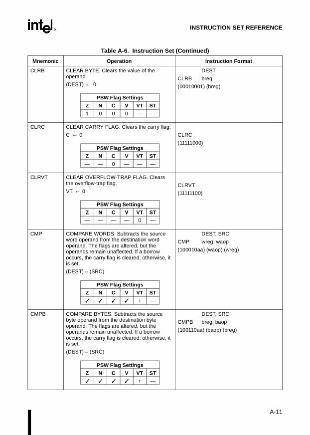
A-11
INSTRUCTION SET REFERENCE
CLRB CLEAR BYTE. Clears the value of the operand.
(DEST) ← 0
DEST
CLRB breg
(00010001) (breg)
PSW Flag Settings
Z N C V VT ST
1 0 0 0 — —
CLRC CLEAR CARRY FLAG. Clears the carry flag.
C ← 0 CLRC
(11111000)PSW Flag Settings
Z N C V VT ST
— — 0 — — —
CLRVT CLEAR OVERFLOW-TRAP FLAG. Clears the overflow-trap flag.
VT ← 0CLRVT
(11111100)
PSW Flag Settings
Z N C V VT ST
— — — — 0 —
CMP COMPARE WORDS. Subtracts the source word operand from the destination word operand. The flags are altered, but the operands remain unaffected. If a borrow occurs, the carry flag is cleared; otherwise, it is set.
(DEST) – (SRC)
DEST, SRC
CMP wreg, waop
(100010aa) (waop) (wreg)
PSW Flag Settings
Z N C V VT ST
↑ —
CMPB COMPARE BYTES. Subtracts the source byte operand from the destination byte operand. The flags are altered, but the operands remain unaffected. If a borrow occurs, the carry flag is cleared; otherwise, it is set.
(DEST) – (SRC)
DEST, SRC
CMPB breg, baop
(100110aa) (baop) (breg)
PSW Flag Settings
Z N C V VT ST
↑ —
Table A-6. Instruction Set (Continued)
Mnemonic Operation Instruction Format

8XC196Kx, Jx, CA USER’S MANUAL
A-12
CMPL COMPARE LONG. Compares the magnitudes of two double-word (long) operands. The operands are specified using the direct addressing mode. The flags are altered, but the operands remain unaffected. If a borrow occurs, the carry flag is cleared; otherwise, it is set.
(DEST) – (SRC)
DEST, SRC
CMPL Dlreg, Slreg
(11000101) (Slreg) (Dlreg)
PSW Flag Settings
Z N C V VT ST
—
DEC DECREMENT WORD. Decrements the value of the operand by one.
(DEST) ← (DEST) –1
DEST
DEC wreg
(00000101) (wreg)
PSW Flag Settings
Z N C V VT ST
↑ —
DECB DECREMENT BYTE. Decrements the value of the operand by one.
(DEST) ← (DEST) –1
DEST
DECB breg
(00010101) (breg)
PSW Flag Settings
Z N C V VT ST
↑ —
DI DISABLE INTERRUPTS. Disables interrupts. Interrupt-calls cannot occur after this instruction.
Interrupt Enable (PSW.1) ← 0
DI
(11111010)
PSW Flag Settings
Z N C V VT ST
— — — — — —
Table A-6. Instruction Set (Continued)
Mnemonic Operation Instruction Format

A-13
INSTRUCTION SET REFERENCE
DIV DIVIDE INTEGERS. Divides the contents of the destination long-integer operand by the contents of the source integer word operand, using signed arithmetic. It stores the quotient into the low-order word of the destination (i.e., the word with the lower address) and the remainder into the high-order word. The following two statements are performed concurrently.
(low word DEST) ← (DEST) / (SRC) (high word DEST) ← (DEST) MOD (SRC)
DEST, SRC
DIV lreg, waop
(11111110) (100011aa) (waop) (lreg)
PSW Flag Settings
Z N C V VT ST
— — — ↑ —
DIVB DIVIDE SHORT-INTEGERS. Divides the contents of the destination integer operand by the contents of the source short-integer operand, using signed arithmetic. It stores the quotient into the low-order byte of the destination (i.e., the word with the lower address) and the remainder into the high-order byte. The following two statements are performed concurrently.
(low byte DEST) ← (DEST) / (SRC) (high byte DEST) ← (DEST) MOD (SRC)
DEST, SRC
DIVB wreg, baop
(11111110) (100111aa) (baop) (wreg)
PSW Flag Settings
Z N C V VT ST
— — — ↑ —
DIVU DIVIDE WORDS, UNSIGNED. Divides the contents of the destination double-word operand by the contents of the source word operand, using unsigned arithmetic. It stores the quotient into the low-order word (i.e., the word with the lower address) of the destination operand and the remainder into the high-order word. The following two statements are performed concurrently.
(low word DEST) ← (DEST) / (SRC) (high word DEST) ← (DEST) MOD (SRC)
DEST, SRC
DIVU lreg, waop
(100011aa) (waop) (lreg)
PSW Flag Settings
Z N C V VT ST
— — — ↑ —
Table A-6. Instruction Set (Continued)
Mnemonic Operation Instruction Format

8XC196Kx, Jx, CA USER’S MANUAL
A-14
DIVUB DIVIDE BYTES, UNSIGNED. This instruction divides the contents of the destination word operand by the contents of the source byte operand, using unsigned arithmetic. It stores the quotient into the low-order byte (i.e., the byte with the lower address) of the destination operand and the remainder into the high-order byte. The following two statements are performed concurrently.
(low byte DEST) ← (DEST) / (SRC) (high byte DEST) ← (DEST) MOD (SRC)
DEST, SRC
DIVUB wreg, baop
(100111aa) (baop) (wreg)
PSW Flag Settings
Z N C V VT ST
— — — ↑ —
DJNZ DECREMENT AND JUMP IF NOT ZERO. Decrements the value of the byte operand by 1. If the result is 0, control passes to the next sequential instruction. If the result is not 0, the instruction adds to the program counter the offset between the end of this instruction and the target label, effecting the jump. The offset must be in the range of –128 to +127.
(COUNT) ← (COUNT) –1 if (COUNT) ≠ 0 then
PC ← PC + 8-bit disp end_if
DJNZ breg,cadd
(11100000) (breg) (disp)
NOTE: The displacement (disp) is sign-extended to 16 bits.
PSW Flag Settings
Z N C V VT ST
— — — — — —
DJNZW DECREMENT AND JUMP IF NOT ZERO WORD. Decrements the value of the word operand by 1. If the result is 0, control passes to the next sequential instruction. If the result is not 0, the instruction adds to the program counter the offset between the end of this instruction and the target label, effecting the jump. The offset must be in the range of –128 to +127
(COUNT) ← (COUNT) –1 if (COUNT) ≠ 0 then
PC ← PC + 8-bit disp end_if
DJNZW wreg,cadd
(11100001) (wreg) (disp)
NOTE: The displacement (disp) is sign-extended to 16 bits.
PSW Flag Settings
Z N C V VT ST
— — — — — —
Table A-6. Instruction Set (Continued)
Mnemonic Operation Instruction Format

A-15
INSTRUCTION SET REFERENCE
DPTS DISABLE PERIPHERAL TRANSACTION SERVER (PTS). Disables the peripheral transaction server (PTS).
PTS Disable (PSW.2) ← 0
DPTS
(11101100)
PSW Flag Settings
Z N C V VT ST
— — — — — —
EI ENABLE INTERRUPTS. Enables interrupts following the execution of the next statement. Interrupt calls cannot occur immediately following this instruction.
Interrupt Enable (PSW.1) ← 1
EI
(11111011)
PSW Flag Settings
Z N C V VT ST
— — — — — —
EPTS ENABLE PERIPHERAL TRANSACTION SERVER (PTS). Enables the peripheral transaction server (PTS).
PTS Enable (PSW.2) ← 1
EPTS
(11101101)
PSW Flag Settings
Z N C V VT ST
— — — — — —
EXT SIGN-EXTEND INTEGER INTO LONG-INTEGER. Sign-extends the low-order word of the operand throughout the high-order word of the operand.
if DEST.15 = 1 then (high word DEST) ← 0FFFFH
else (high word DEST) ← 0
end_if
EXT lreg
(00000110) (lreg)
PSW Flag Settings
Z N C V VT ST
0 0 — —
Table A-6. Instruction Set (Continued)
Mnemonic Operation Instruction Format
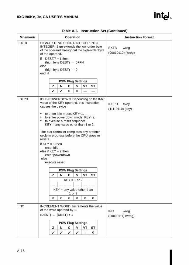
8XC196Kx, Jx, CA USER’S MANUAL
A-16
EXTB SIGN-EXTEND SHORT-INTEGER INTO INTEGER. Sign-extends the low-order byte of the operand throughout the high-order byte of the operand.
if DEST.7 = 1 then (high byte DEST) ← 0FFH
else (high byte DEST) ← 0
end_if
EXTB wreg
(00010110) (wreg)
PSW Flag Settings
Z N C V VT ST
0 0 — —
IDLPD IDLE/POWERDOWN. Depending on the 8-bit value of the KEY operand, this instruction causes the device
• to enter idle mode, KEY=1, • to enter powerdown mode, KEY=2, • to execute a reset sequence,
KEY = any value other than 1 or 2.
The bus controller completes any prefetch cycle in progress before the CPU stops or resets.
if KEY = 1 then enter idle
else if KEY = 2 thenenter powerdown
else execute reset
IDLPD #key
(11110110) (key)
PSW Flag Settings
Z N C V VT ST
KEY = 1 or 2
— — — — — —
KEY = any value other than 1 or 2
0 0 0 0 0 0
INC INCREMENT WORD. Increments the value of the word operand by 1.
(DEST) ← (DEST) + 1INC wreg
(00000111) (wreg)
PSW Flag Settings
Z N C V VT ST
↑ 0
Table A-6. Instruction Set (Continued)
Mnemonic Operation Instruction Format

A-17
INSTRUCTION SET REFERENCE
INCB INCREMENT BYTE. Increments the value of the byte operand by 1.
(DEST) ← (DEST) + 1INCB breg
(00010111) (breg)
PSW Flag Settings
Z N C V VT ST
↑ —
JBC JUMP IF BIT IS CLEAR. Tests the specified bit. If the bit is set, control passes to the next sequential instruction. If the bit is clear, this instruction adds to the program counter the offset between the end of this instruction and the target label, effecting the jump. The offset must be in the range of –128 to +127.
if (specified bit) = 0 then PC ← PC + 8-bit disp
JBC breg,bitno,cadd
(00110bbb) (breg) (disp)
NOTE: The displacement (disp) is sign-extended to 16 bits.
PSW Flag Settings
Z N C V VT ST
— — — — — —
JBS JUMP IF BIT IS SET. Tests the specified bit. If the bit is clear, control passes to the next sequential instruction. If the bit is set, this instruction adds to the program counter the offset between the end of this instruction and the target label, effecting the jump. The offset must be in the range of –128 to +127.
if (specified bit) = 1 then PC ← PC + 8-bit disp
JBS breg,bitno,cadd
(00111bbb) (breg) (disp)
NOTE: The displacement (disp) is sign-extended to 16 bits.
PSW Flag Settings
Z N C V VT ST
— — — — — —
Table A-6. Instruction Set (Continued)
Mnemonic Operation Instruction Format

8XC196Kx, Jx, CA USER’S MANUAL
A-18
JC JUMP IF CARRY FLAG IS SET. Tests the carry flag. If the carry flag is clear, control passes to the next sequential instruction. If the carry flag is set, this instruction adds to the program counter the offset between the end of this instruction and the target label, effecting the jump. The offset must be in the range of –128 to +127.
if C = 1 then PC ← PC + 8-bit disp
JC cadd
(11011011) (disp)
NOTE: The displacement (disp) is sign-extended to 16 bits.
PSW Flag Settings
Z N C V VT ST
— — — — — —
JE JUMP IF EQUAL. Tests the zero flag. If the flag is clear, control passes to the next sequential instruction. If the zero flag is set, this instruction adds to the program counter the offset between the end of this instruction and the target label, effecting the jump. The offset must be in the range of –128 to +127.
if Z = 1 then PC ← PC + 8-bit disp
JE cadd
(11011111) (disp)
NOTE: The displacement (disp) is sign-extended to 16 bits.
PSW Flag Settings
Z N C V VT ST
— — — — — —
JGE JUMP IF SIGNED GREATER THAN OR EQUAL. Tests the negative flag. If the negative flag is set, control passes to the next sequential instruction. If the negative flag is clear, this instruction adds to the program counter the offset between the end of this instruction and the target label, effecting the jump. The offset must be in the range of –128 to +127.
if N = 0 then PC ← PC + 8-bit disp
JGE cadd
(11010110) (disp)
NOTE: The displacement (disp) is sign-extended to 16 bits.
PSW Flag Settings
Z N C V VT ST
— — — — — —
Table A-6. Instruction Set (Continued)
Mnemonic Operation Instruction Format

A-19
INSTRUCTION SET REFERENCE
JGT JUMP IF SIGNED GREATER THAN. Tests both the zero flag and the negative flag. If either flag is set, control passes to the next sequential instruction. If both flags are clear, this instruction adds to the program counter the offset between the end of this instruction and the target label, effecting the jump. The offset must be in the range of –128 to +127.
if N = 0 AND Z = 0 then PC ← PC + 8-bit disp
JGT cadd
(11010010) (disp)
NOTE: The displacement (disp) is sign-extended to 16 bits.
PSW Flag Settings
Z N C V VT ST
— — — — — —
JH JUMP IF HIGHER (UNSIGNED). Tests both the zero flag and the carry flag. If either the carry flag is clear or the zero flag is set, control passes to the next sequential instruction. If the carry flag is set and the zero flag is clear, this instruction adds to the program counter the offset between the end of this instruction and the target label, effecting the jump. The offset must be in range of –128 to +127.
if C = 1 AND Z = 0 then PC ← PC + 8-bit disp
JH cadd
(11011001) (disp)
NOTE: The displacement (disp) is sign-extended to 16 bits.
PSW Flag Settings
Z N C V VT ST
— — — — — —
JLE JUMP IF SIGNED LESS THAN OR EQUAL. Tests both the negative flag and the zero flag. If both flags are clear, control passes to the next sequential instruction. If either flag is set, this instruction adds to the program counter the offset between the end of this instruction and the target label, effecting the jump. The offset must be in the range of –128 to +127.
if N = 1 OR Z = 1 then PC ← PC + 8-bit disp
JLE cadd
(11011010) (disp)
NOTE: The displacement (disp) is sign-extended to 16 bits.
PSW Flag Settings
Z N C V VT ST
— — — — — —
Table A-6. Instruction Set (Continued)
Mnemonic Operation Instruction Format
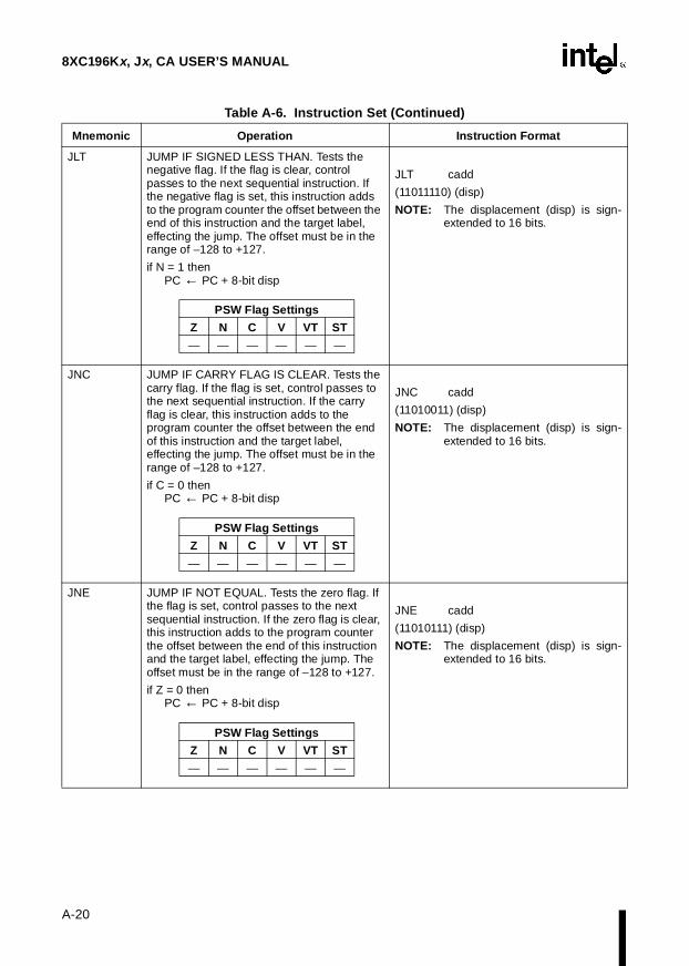
8XC196Kx, Jx, CA USER’S MANUAL
A-20
JLT JUMP IF SIGNED LESS THAN. Tests the negative flag. If the flag is clear, control passes to the next sequential instruction. If the negative flag is set, this instruction adds to the program counter the offset between the end of this instruction and the target label, effecting the jump. The offset must be in the range of –128 to +127.
if N = 1 then PC ← PC + 8-bit disp
JLT cadd
(11011110) (disp)
NOTE: The displacement (disp) is sign-extended to 16 bits.
PSW Flag Settings
Z N C V VT ST
— — — — — —
JNC JUMP IF CARRY FLAG IS CLEAR. Tests the carry flag. If the flag is set, control passes to the next sequential instruction. If the carry flag is clear, this instruction adds to the program counter the offset between the end of this instruction and the target label, effecting the jump. The offset must be in the range of –128 to +127.
if C = 0 then PC ← PC + 8-bit disp
JNC cadd
(11010011) (disp)
NOTE: The displacement (disp) is sign-extended to 16 bits.
PSW Flag Settings
Z N C V VT ST
— — — — — —
JNE JUMP IF NOT EQUAL. Tests the zero flag. If the flag is set, control passes to the next sequential instruction. If the zero flag is clear, this instruction adds to the program counter the offset between the end of this instruction and the target label, effecting the jump. The offset must be in the range of –128 to +127.
if Z = 0 then PC ← PC + 8-bit disp
JNE cadd
(11010111) (disp)
NOTE: The displacement (disp) is sign-extended to 16 bits.
PSW Flag Settings
Z N C V VT ST
— — — — — —
Table A-6. Instruction Set (Continued)
Mnemonic Operation Instruction Format

A-21
INSTRUCTION SET REFERENCE
JNH JUMP IF NOT HIGHER (UNSIGNED). Tests both the zero flag and the carry flag. If the carry flag is set and the zero flag is clear, control passes to the next sequential instruction. If either the carry flag is clear or the zero flag is set, this instruction adds to the program counter the offset between the end of this instruction and the target label, effecting the jump. The offset must be in range of –128 to +127.
if C = 0 OR Z = 1 then PC ← PC + 8-bit disp
JNH cadd
(11010001) (disp)
NOTE: The displacement (disp) is sign-extended to 16 bits.
PSW Flag Settings
Z N C V VT ST
— — — — — —
JNST JUMP IF STICKY BIT FLAG IS CLEAR. Tests the sticky bit flag. If the flag is set, control passes to the next sequential instruction. If the sticky bit flag is clear, this instruction adds to the program counter the offset between the end of this instruction and the target label, effecting the jump. The offset must be in range of –128 to +127.
if ST = 0 then PC ← PC + 8-bit disp
JNST cadd
(11010000) (disp)
NOTE: The displacement (disp) is sign-extended to 16 bits.
PSW Flag Settings
Z N C V VT ST
— — — — — —
JNV JUMP IF OVERFLOW FLAG IS CLEAR. Tests the overflow flag. If the flag is set, control passes to the next sequential instruction. If the overflow flag is clear, this instruction adds to the program counter the offset between the end of this instruction and the target label, effecting the jump. The offset must be in range of –128 to +127.
if V = 0 then PC ← PC + 8-bit disp
JNV cadd
(11010101) (disp)
NOTE: The displacement (disp) is sign-extended to 16 bits.
PSW Flag Settings
Z N C V VT ST
— — — — — —
Table A-6. Instruction Set (Continued)
Mnemonic Operation Instruction Format

8XC196Kx, Jx, CA USER’S MANUAL
A-22
JNVT JUMP IF OVERFLOW-TRAP FLAG IS CLEAR. Tests the overflow-trap flag. If the flag is set, this instruction clears the flag and passes control to the next sequential instruction. If the overflow-trap flag is clear, this instruction adds to the program counter the offset between the end of this instruction and the target label, effecting the jump. The offset must be in range of –128 to +127.
if VT = 0 then PC ← PC + 8-bit disp
JNVT cadd
(11010100) (disp)
NOTE: The displacement (disp) is sign-extended to 16 bits.
PSW Flag Settings
Z N C V VT ST
— — — — 0 —
JST JUMP IF STICKY BIT FLAG IS SET. Tests the sticky bit flag. If the flag is clear, control passes to the next sequential instruction. If the sticky bit flag is set, this instruction adds to the program counter the offset between the end of this instruction and the target label, effecting the jump. The offset must be in range of –128 to +127.
if ST = 1 then PC ← PC + 8-bit disp
JST cadd
(11011000) (disp)
NOTE: The displacement (disp) is sign-extended to 16 bits.
PSW Flag Settings
Z N C V VT ST
— — — — — —
JV JUMP IF OVERFLOW FLAG IS SET. Tests the overflow flag. If the flag is clear, control passes to the next sequential instruction. If the overflow flag is set, this instruction adds to the program counter the offset between the end of this instruction and the target label, effecting the jump. The offset must be in range of –128 to +127.
if V = 1 then PC ← PC + 8-bit disp
JV cadd
(11011101) (disp)
NOTE: The displacement (disp) is sign-extended to 16 bits.
PSW Flag Settings
Z N C V VT ST
— — — — — —
Table A-6. Instruction Set (Continued)
Mnemonic Operation Instruction Format

A-23
INSTRUCTION SET REFERENCE
JVT JUMP IF OVERFLOW-TRAP FLAG IS SET. Tests the overflow-trap flag. If the flag is clear, control passes to the next sequential instruction. If the overflow-trap flag is set, this instruction clears the flag and adds to the program counter the offset between the end of this instruction and the target label, effecting the jump. The offset must be in range of –128 to +127.
if VT = 1 then PC ← PC + 8-bit disp
JVT cadd
(11011100) (disp)
NOTE: The displacement (disp) is sign-extended to 16 bits.
PSW Flag Settings
Z N C V VT ST
— — — — 0 —
LCALL LONG CALL. Pushes the contents of the program counter (the return address) onto the stack, then adds to the program counter the offset between the end of this instruction and the target label, effecting the call. The offset must be in the range of –32,768 to +32,767.
SP ← SP – 2(SP) ← PCPC ← PC + 16-bit disp
LCALL cadd
(11101111) (disp-low) (disp-high)
PSW Flag Settings
Z N C V VT ST
— — — — — —
LD LOAD WORD. Loads the value of the source word operand into the destination operand.
(DEST) ← (SRC)
DEST, SRC
LD wreg, waop
(101000aa) (waop) (wreg)
PSW Flag Settings
Z N C V VT ST
— — — — — —
LDB LOAD BYTE. Loads the value of the source byte operand into the destination operand.
(DEST) ← (SRC)
DEST, SRC
LDB breg, baop
(101100aa) (baop) (breg)
PSW Flag Settings
Z N C V VT ST
— — — — — —
Table A-6. Instruction Set (Continued)
Mnemonic Operation Instruction Format

8XC196Kx, Jx, CA USER’S MANUAL
A-24
LDBSE LOAD BYTE SIGN-EXTENDED. Sign-extends the value of the source short-integer operand and loads it into the destination integer operand.
(low byte DEST) ← (SRC)
if DEST.15 = 1 then (high word DEST) ← 0FFH
else (high word DEST) ← 0
end_if
DEST, SRC
LDBSE wreg, baop
(101111aa) (baop) (wreg)
PSW Flag Settings
Z N C V VT ST
— — — — — —
LDBZE LOAD BYTE ZERO-EXTENDED. Zero-extends the value of the source byte operand and loads it into the destination word operand.
(low byte DEST) ← (SRC) (high byte DEST) ← 0
DEST, SRC
LDBZE wreg, baop
(101011aa) (baop) (wreg)
PSW Flag Settings
Z N C V VT ST
— — — — — —
LJMP LONG JUMP. Adds to the program counter the offset between the end of this instruction and the target label, effecting the jump. The offset must be in the range of –32,768 to +32,767.
PC ← PC + 16-bit disp
LJMP cadd
(11100111) (disp-low) (disp-high)
PSW Flag Settings
Z N C V VT ST
— — — — — ?
MUL (2 operands)
MULTIPLY INTEGERS. Multiplies the source and destination integer operands, using signed arithmetic, and stores the 32-bit result into the destination long-integer operand. The sticky bit flag is undefined after the instruction is executed.
(DEST) ← (DEST) × (SRC)
DEST, SRC
MUL lreg, waop
(11111110) (011011aa) (waop) (lreg)
PSW Flag Settings
Z N C V VT ST
— — — — — ?
Table A-6. Instruction Set (Continued)
Mnemonic Operation Instruction Format
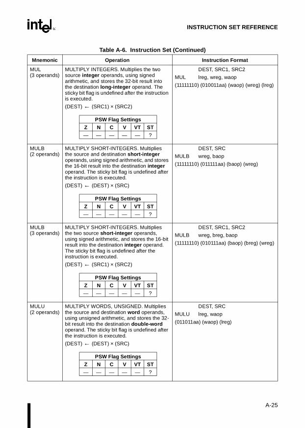
A-25
INSTRUCTION SET REFERENCE
MUL (3 operands)
MULTIPLY INTEGERS. Multiplies the two source integer operands, using signed arithmetic, and stores the 32-bit result into the destination long-integer operand. The sticky bit flag is undefined after the instruction is executed.
(DEST) ← (SRC1) × (SRC2)
DEST, SRC1, SRC2
MUL lreg, wreg, waop
(11111110) (010011aa) (waop) (wreg) (lreg)
PSW Flag Settings
Z N C V VT ST
— — — — — ?
MULB (2 operands)
MULTIPLY SHORT-INTEGERS. Multiplies the source and destination short-integer operands, using signed arithmetic, and stores the 16-bit result into the destination integer operand. The sticky bit flag is undefined after the instruction is executed.
(DEST) ← (DEST) × (SRC)
DEST, SRC
MULB wreg, baop
(11111110) (011111aa) (baop) (wreg)
PSW Flag Settings
Z N C V VT ST
— — — — — ?
MULB (3 operands)
MULTIPLY SHORT-INTEGERS. Multiplies the two source short-integer operands, using signed arithmetic, and stores the 16-bit result into the destination integer operand. The sticky bit flag is undefined after the instruction is executed.
(DEST) ← (SRC1) × (SRC2)
DEST, SRC1, SRC2
MULB wreg, breg, baop
(11111110) (010111aa) (baop) (breg) (wreg)
PSW Flag Settings
Z N C V VT ST
— — — — — ?
MULU (2 operands)
MULTIPLY WORDS, UNSIGNED. Multiplies the source and destination word operands, using unsigned arithmetic, and stores the 32-bit result into the destination double-word operand. The sticky bit flag is undefined after the instruction is executed.
(DEST) ← (DEST) × (SRC)
DEST, SRC
MULU lreg, waop
(011011aa) (waop) (lreg)
PSW Flag Settings
Z N C V VT ST
— — — — — ?
Table A-6. Instruction Set (Continued)
Mnemonic Operation Instruction Format
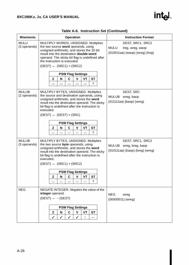
8XC196Kx, Jx, CA USER’S MANUAL
A-26
MULU (3 operands)
MULTIPLY WORDS, UNSIGNED. Multiplies the two source word operands, using unsigned arithmetic, and stores the 32-bit result into the destination double-word operand. The sticky bit flag is undefined after the instruction is executed.
(DEST) ← (SRC1) × (SRC2)
DEST, SRC1, SRC2
MULU lreg, wreg, waop
(010011aa) (waop) (wreg) (lreg)
PSW Flag Settings
Z N C V VT ST
— — — — — ?
MULUB (2 operands)
MULTIPLY BYTES, UNSIGNED. Multiplies the source and destination operands, using unsigned arithmetic, and stores the word result into the destination operand. The sticky bit flag is undefined after the instruction is executed.
(DEST) ← (DEST) × (SRC)
DEST, SRC
MULUB wreg, baop
(011111aa) (baop) (wreg)
PSW Flag Settings
Z N C V VT ST
— — — — — ?
MULUB (3 operands)
MULTIPLY BYTES, UNSIGNED. Multiplies the two source byte operands, using unsigned arithmetic, and stores the word result into the destination operand. The sticky bit flag is undefined after the instruction is executed.
(DEST) ← (SRC1) × (SRC2)
DEST, SRC1, SRC2
MULUB wreg, breg, baop
(010111aa) (baop) (breg) (wreg)
PSW Flag Settings
Z N C V VT ST
— — — — — ?
NEG NEGATE INTEGER. Negates the value of the integer operand.
(DEST) ← – (DEST)NEG wreg
(00000011) (wreg)
PSW Flag Settings
Z N C V VT ST
↑ —
Table A-6. Instruction Set (Continued)
Mnemonic Operation Instruction Format

A-27
INSTRUCTION SET REFERENCE
NEGB NEGATE SHORT-INTEGER. Negates the value of the short-integer operand.
(DEST) ← – (DEST)NEGB breg
(00010011) (breg)
PSW Flag Settings
Z N C V VT ST
↑ —
NOP NO OPERATION. Does nothing. Control passes to the next sequential instruction. NOP
(11111101)PSW Flag Settings
Z N C V VT ST
— — — — — —
NORML NORMALIZE LONG-INTEGER. Normalizes the source (leftmost) long-integer operand. (That is, it shifts the operand to the left until its most significant bit is “1” or until it has performed 31 shifts). If the most significant bit is still “0” after 31 shifts, the instruction stops the process and sets the zero flag. The instruction stores the actual number of shifts performed in the destination (rightmost) operand.
(COUNT) ← 0 do while
(MSB (DEST) = 0) AND (COUNT) < 31)(DEST) ← (DEST) × 2 (COUNT) ← (COUNT) + 1
end_while
SRC, DEST
NORML lreg, breg
(00001111) (breg) (lreg)
PSW Flag Settings
Z N C V VT ST
? 0 — — —
NOT COMPLEMENT WORD. Complements the value of the word operand (replaces each “1” with a “0” and each “0” with a “1”).
(DEST) ← NOT (DEST)
NOT wreg
(00000010) (wreg)
PSW Flag Settings
Z N C V VT ST
0 0 — —
Table A-6. Instruction Set (Continued)
Mnemonic Operation Instruction Format
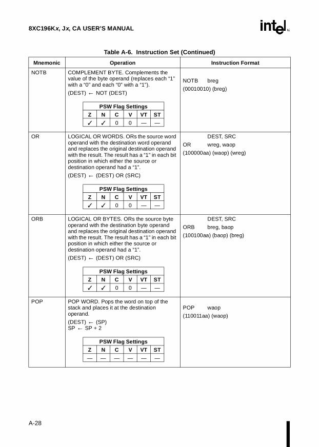
8XC196Kx, Jx, CA USER’S MANUAL
A-28
NOTB COMPLEMENT BYTE. Complements the value of the byte operand (replaces each “1” with a “0” and each “0” with a “1”).
(DEST) ← NOT (DEST)
NOTB breg
(00010010) (breg)
PSW Flag Settings
Z N C V VT ST
0 0 — —
OR LOGICAL OR WORDS. ORs the source word operand with the destination word operand and replaces the original destination operand with the result. The result has a “1” in each bit position in which either the source or destination operand had a “1”.
(DEST) ← (DEST) OR (SRC)
DEST, SRC
OR wreg, waop
(100000aa) (waop) (wreg)
PSW Flag Settings
Z N C V VT ST
0 0 — —
ORB LOGICAL OR BYTES. ORs the source byte operand with the destination byte operand and replaces the original destination operand with the result. The result has a “1” in each bit position in which either the source or destination operand had a “1”.
(DEST) ← (DEST) OR (SRC)
DEST, SRC
ORB breg, baop
(100100aa) (baop) (breg)
PSW Flag Settings
Z N C V VT ST
0 0 — —
POP POP WORD. Pops the word on top of the stack and places it at the destination operand.
(DEST) ← (SP) SP ← SP + 2
POP waop
(110011aa) (waop)
PSW Flag Settings
Z N C V VT ST
— — — — — —
Table A-6. Instruction Set (Continued)
Mnemonic Operation Instruction Format

A-29
INSTRUCTION SET REFERENCE
POPA POP ALL. This instruction is used instead of POPF, to support the eight additional interrupts. It pops two words off the stack and places the first word into the INT_MASK1/WSR register pair and the second word into the PSW/INT_MASK register-pair. This instruction increments the SP by 4. Interrupt-calls cannot occur immediately following this instruction.
INT_MASK1/WSR ← (SP) SP ← SP + 2 PSW/INT_MASK ← (SP) SP ← SP + 2
POPA
(11110101)
PSW Flag Settings
Z N C V VT ST
POPF POP FLAGS. Pops the word on top of the stack and places it into the PSW. Interrupt-calls cannot occur immediately following this instruction.
(PSW) ← (SP) SP ← SP + 2
POPF
(11110011)
PSW Flag Settings
Z N C V VT ST
PUSH PUSH WORD. Pushes the word operand onto the stack.
SP ← SP – 2 (SP) ← (DEST)
PUSH waop
(110010aa) (waop)
PSW Flag Settings
Z N C V VT ST
— — — — — —
Table A-6. Instruction Set (Continued)
Mnemonic Operation Instruction Format

8XC196Kx, Jx, CA USER’S MANUAL
A-30
PUSHA PUSH ALL. This instruction is used instead of PUSHF, to support the eight additional interrupts. It pushes two words — PSW/INT_MASK and INT_MASK1/WSR — onto the stack.
This instruction clears the PSW, INT_MASK, and INT_MASK1 registers and decrements the SP by 4. Interrupt-calls cannot occur immediately following this instruction.
SP ← SP – 2 (SP) ← PSW/INT_MASK PSW/INT_MASK ← 0 SP ← SP – 2 (SP) ← INT_MASK1/WSR INT_MASK1 ← 0
PUSHA
(11110100)
PSW Flag Settings
Z N C V VT ST
0 0 0 0 0 0
PUSHF PUSH FLAGS. Pushes the PSW onto the top of the stack, then clears it. Clearing the PSW disables interrupt servicing. Interrupt-calls cannot occur immediately following this instruction.
SP ← SP – 2 (SP) ← PSW/INT_MASK PSW/INT_MASK ← 0
PUSHF
(11110010)
PSW Flag Settings
Z N C V VT ST
0 0 0 0 0 0
RET RETURN FROM SUBROUTINE. Pops the PC off the top of the stack.
PC ← (SP) SP ← SP + 2
RET
(11110000)
PSW Flag Settings
Z N C V VT ST
— — — — — —
Table A-6. Instruction Set (Continued)
Mnemonic Operation Instruction Format

A-31
INSTRUCTION SET REFERENCE
RST RESET SYSTEM. Initializes the PSW to zero, the PC to 2080H, and the pins and SFRs to their reset values. Executing this instruction causes the RESET# pin to be pulled low for 16 state times.
SFR ← Reset Status Pin ← Reset Status PSW ← 0 PC ← 2080H
RST
(11111111)
PSW Flag Settings
Z N C V VT ST
0 0 0 0 0 0
SCALL SHORT CALL. Pushes the contents of the program counter (the return address) onto the stack, then adds to the program counter the offset between the end of this instruction and the target label, effecting the call. The offset must be in the range of –1024 to +1023.
SP ← SP – 2 (SP) ← PC PC←PC+11-bit disp
SCALL cadd
(00101xxx) (disp-low)
NOTE: The displacement (disp) is sign-extended to 16-bits.
PSW Flag Settings
Z N C V VT ST
— — — — — —
SETC SET CARRY FLAG. Sets the carry flag.
C ← 1 SETC
(11111001)PSW Flag Settings
Z N C V VT ST
— — 1 — — —
Table A-6. Instruction Set (Continued)
Mnemonic Operation Instruction Format

8XC196Kx, Jx, CA USER’S MANUAL
A-32
SHL SHIFT WORD LEFT. Shifts the destination word operand to the left as many times as specified by the count operand. The count may be specified either as an immediate value in the range of 0 to 15 (0FH), inclusive, or as the content of any register (10H – 0FFH) with a value in the range of 0 to 31 (1FH), inclusive. The right bits of the result are filled with zeroes. The last bit shifted out is saved in the carry flag.
Temp ← (COUNT) do while Temp ≠ 0
C ← High order bit of (DEST) (DEST) ← (DEST) × 2 Temp ← Temp – 1
end_while
SHL wreg,#count
(00001001) (count) (wreg)
or
SHL wreg,breg
(00001001) (breg) (wreg)
PSW Flag Settings
Z N C V VT ST
↑ —
SHLB SHIFT BYTE LEFT. Shifts the destination byte operand to the left as many times as specified by the count operand. The count may be specified either as an immediate value in the range of 0 to 15 (0FH), inclusive, or as the content of any register (10H – 0FFH) with a value in the range of 0 to 31 (1FH), inclusive. The right bits of the result are filled with zeroes. The last bit shifted out is saved in the carry flag.
Temp ← (COUNT) do while Temp ≠ 0
C ← High order bit of (DEST) (DEST) ← (DEST) × 2 Temp ← Temp – 1
end_while
SHLB breg,#count
(00011001) (count) (breg)
or
SHLB breg,breg
(00011001) (breg) (breg)
PSW Flag Settings
Z N C V VT ST
↑ —
Table A-6. Instruction Set (Continued)
Mnemonic Operation Instruction Format
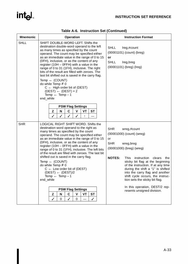
A-33
INSTRUCTION SET REFERENCE
SHLL SHIFT DOUBLE-WORD LEFT. Shifts the destination double-word operand to the left as many times as specified by the count operand. The count may be specified either as an immediate value in the range of 0 to 15 (0FH), inclusive, or as the content of any register (10H – 0FFH) with a value in the range of 0 to 31 (1FH), inclusive. The right bits of the result are filled with zeroes. The last bit shifted out is saved in the carry flag.
Temp ← (COUNT) do while Temp ≠ 0
C ← High order bit of (DEST) (DEST) ← (DEST) × 2 Temp ← Temp – 1
end_while
SHLL lreg,#count
(00001101) (count) (breg)
or
SHLL lreg,breg
(00001101) (breg) (lreg)
PSW Flag Settings
Z N C V VT ST
↑ —
SHR LOGICAL RIGHT SHIFT WORD. Shifts the destination word operand to the right as many times as specified by the count operand. The count may be specified either as an immediate value in the range of 0 to 15 (0FH), inclusive, or as the content of any register (10H – 0FFH) with a value in the range of 0 to 31 (1FH), inclusive. The left bits of the result are filled with zeroes. The last bit shifted out is saved in the carry flag.
Temp ← (COUNT) do while Temp ≠ 0
C ← Low order bit of (DEST) (DEST) ← (DEST)/2Temp ← Temp – 1
end_while
SHR wreg,#count
(00001000) (count) (wreg)
or
SHR wreg,breg
(00001000) (breg) (wreg)
NOTES: This instruction clears thesticky bit flag at the beginningof the instruction. If at any timeduring the shift a “1” is shiftedinto the carry flag and anothershift cycle occurs, the instruc-tion sets the sticky bit flag.
In this operation, DEST/2 rep-resents unsigned division.PSW Flag Settings
Z N C V VT ST
0 0 —
Table A-6. Instruction Set (Continued)
Mnemonic Operation Instruction Format

8XC196Kx, Jx, CA USER’S MANUAL
A-34
SHRA ARITHMETIC RIGHT SHIFT WORD. Shifts the destination word operand to the right as many times as specified by the count operand. The count may be specified either as an immediate value in the range of 0 to 15 (0FH), inclusive, or as the content of any register (10H – 0FFH) with a value in the range of 0 to 31 (1FH), inclusive. If the original high order bit value was “0,” zeroes are shifted in. If the value was “1,” ones are shifted in. The last bit shifted out is saved in the carry flag.
Temp ← (COUNT) do while Temp ≠ 0
C ← Low order bit of (DEST) (DEST) ← (DEST)/2 Temp ← Temp – 1
end_while
SHRA wreg,#count
(00001010) (count) (wreg)
or
SHRA wreg,breg
(00001010) (breg) (wreg)
NOTE: This instruction clears the stickybit flag at the beginning of theinstruction. If at any time duringthe shift a “1” is shifted into thecarry flag and another shift cycleoccurs, the instruction sets thesticky bit flag.
In this operation, DEST/2 repre-sents signed division.
PSW Flag Settings
Z N C V VT ST
0 —
SHRAB ARITHMETIC RIGHT SHIFT BYTE. Shifts the destination byte operand to the right as many times as specified by the count operand. The count may be specified either as an immediate value in the range of 0 to 15 (0FH), inclusive, or as the content of any register (10H – 0FFH) with a value in the range of 0 to 31 (1FH), inclusive. If the original high order bit value was “0,” zeroes are shifted in. If the value was “1,” ones are shifted in. The last bit shifted out is saved in the carry flag.
Temp ← (COUNT) do while Temp ≠ 0
C = Low order bit of (DEST) (DEST) ← (DEST)/2Temp ← Temp – 1
end_while
SHRAB breg,#count
(00011010) (count) (breg)
or
SHRAB breg,breg
(00011010) (breg) (breg)
NOTES: This instruction clears thesticky bit flag at the beginningof the instruction. If at any timeduring the shift a “1” is shiftedinto the carry flag and anothershift cycle occurs, the instruc-tion sets the sticky bit flag.
In this operation, DEST/2 rep-resents signed division.
PSW Flag Settings
Z N C V VT ST
0 —
Table A-6. Instruction Set (Continued)
Mnemonic Operation Instruction Format
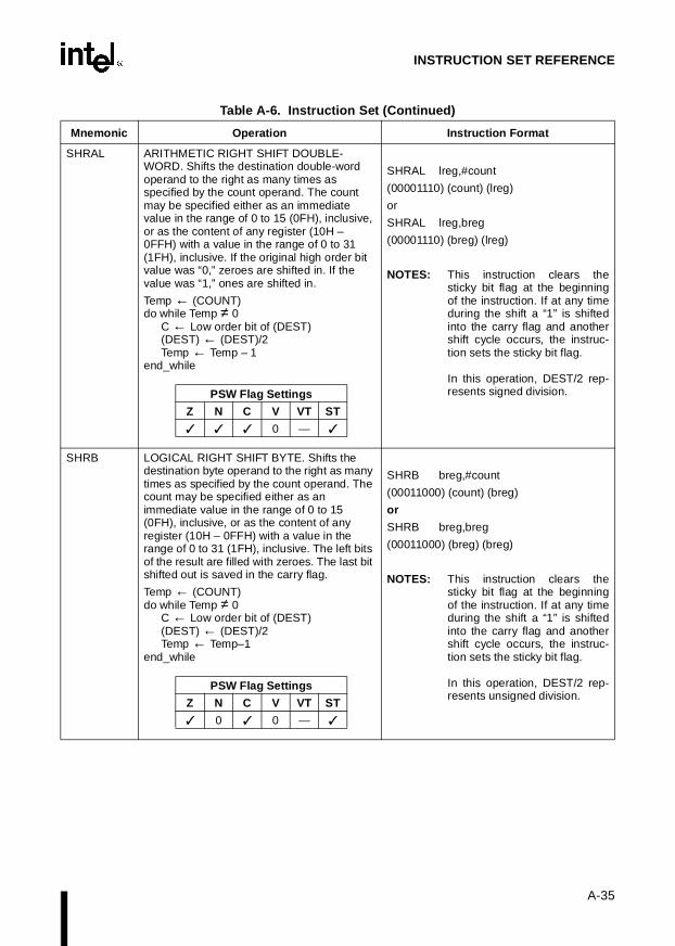
A-35
INSTRUCTION SET REFERENCE
SHRAL ARITHMETIC RIGHT SHIFT DOUBLE-WORD. Shifts the destination double-word operand to the right as many times as specified by the count operand. The count may be specified either as an immediate value in the range of 0 to 15 (0FH), inclusive, or as the content of any register (10H – 0FFH) with a value in the range of 0 to 31 (1FH), inclusive. If the original high order bit value was “0,” zeroes are shifted in. If the value was “1,” ones are shifted in.
Temp ← (COUNT) do while Temp ≠ 0
C ← Low order bit of (DEST) (DEST) ← (DEST)/2 Temp ← Temp – 1
end_while
SHRAL lreg,#count
(00001110) (count) (lreg)
or
SHRAL lreg,breg
(00001110) (breg) (lreg)
NOTES: This instruction clears thesticky bit flag at the beginningof the instruction. If at any timeduring the shift a “1” is shiftedinto the carry flag and anothershift cycle occurs, the instruc-tion sets the sticky bit flag.
In this operation, DEST/2 rep-resents signed division.PSW Flag Settings
Z N C V VT ST
0 —
SHRB LOGICAL RIGHT SHIFT BYTE. Shifts the destination byte operand to the right as many times as specified by the count operand. The count may be specified either as an immediate value in the range of 0 to 15 (0FH), inclusive, or as the content of any register (10H – 0FFH) with a value in the range of 0 to 31 (1FH), inclusive. The left bits of the result are filled with zeroes. The last bit shifted out is saved in the carry flag.
Temp ← (COUNT) do while Temp ≠ 0
C ← Low order bit of (DEST) (DEST) ← (DEST)/2 Temp ← Temp–1
end_while
SHRB breg,#count
(00011000) (count) (breg)
or
SHRB breg,breg
(00011000) (breg) (breg)
NOTES: This instruction clears thesticky bit flag at the beginningof the instruction. If at any timeduring the shift a “1” is shiftedinto the carry flag and anothershift cycle occurs, the instruc-tion sets the sticky bit flag.
In this operation, DEST/2 rep-resents unsigned division.
PSW Flag Settings
Z N C V VT ST
0 0 —
Table A-6. Instruction Set (Continued)
Mnemonic Operation Instruction Format
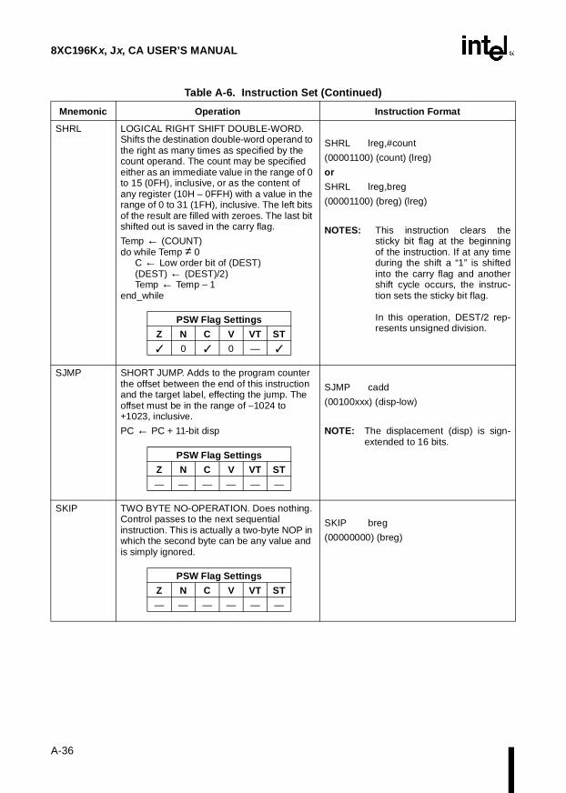
8XC196Kx, Jx, CA USER’S MANUAL
A-36
SHRL LOGICAL RIGHT SHIFT DOUBLE-WORD. Shifts the destination double-word operand to the right as many times as specified by the count operand. The count may be specified either as an immediate value in the range of 0 to 15 (0FH), inclusive, or as the content of any register (10H – 0FFH) with a value in the range of 0 to 31 (1FH), inclusive. The left bits of the result are filled with zeroes. The last bit shifted out is saved in the carry flag.
Temp ← (COUNT) do while Temp ≠ 0
C ← Low order bit of (DEST) (DEST) ← (DEST)/2)Temp ← Temp – 1
end_while
SHRL lreg,#count
(00001100) (count) (lreg)
or
SHRL lreg,breg
(00001100) (breg) (lreg)
NOTES: This instruction clears thesticky bit flag at the beginningof the instruction. If at any timeduring the shift a “1” is shiftedinto the carry flag and anothershift cycle occurs, the instruc-tion sets the sticky bit flag.
In this operation, DEST/2 rep-resents unsigned division.
PSW Flag Settings
Z N C V VT ST
0 0 —
SJMP SHORT JUMP. Adds to the program counter the offset between the end of this instruction and the target label, effecting the jump. The offset must be in the range of –1024 to +1023, inclusive.
PC ← PC + 11-bit disp
SJMP cadd
(00100xxx) (disp-low)
NOTE: The displacement (disp) is sign-extended to 16 bits.
PSW Flag Settings
Z N C V VT ST
— — — — — —
SKIP TWO BYTE NO-OPERATION. Does nothing. Control passes to the next sequential instruction. This is actually a two-byte NOP in which the second byte can be any value and is simply ignored.
SKIP breg
(00000000) (breg)
PSW Flag Settings
Z N C V VT ST
— — — — — —
Table A-6. Instruction Set (Continued)
Mnemonic Operation Instruction Format
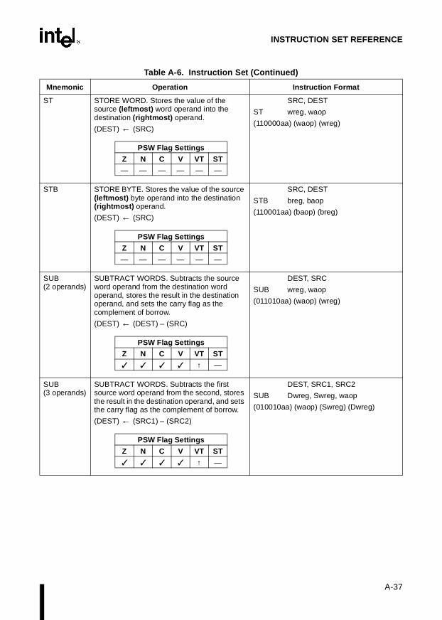
A-37
INSTRUCTION SET REFERENCE
ST STORE WORD. Stores the value of the source (leftmost) word operand into the destination (rightmost) operand.
(DEST) ← (SRC)
SRC, DEST
ST wreg, waop
(110000aa) (waop) (wreg)
PSW Flag Settings
Z N C V VT ST
— — — — — —
STB STORE BYTE. Stores the value of the source (leftmost) byte operand into the destination (rightmost) operand.
(DEST) ← (SRC)
SRC, DEST
STB breg, baop
(110001aa) (baop) (breg)
PSW Flag Settings
Z N C V VT ST
— — — — — —
SUB (2 operands)
SUBTRACT WORDS. Subtracts the source word operand from the destination word operand, stores the result in the destination operand, and sets the carry flag as the complement of borrow.
(DEST) ← (DEST) – (SRC)
DEST, SRC
SUB wreg, waop
(011010aa) (waop) (wreg)
PSW Flag Settings
Z N C V VT ST
↑ —
SUB (3 operands)
SUBTRACT WORDS. Subtracts the first source word operand from the second, stores the result in the destination operand, and sets the carry flag as the complement of borrow.
(DEST) ← (SRC1) – (SRC2)
DEST, SRC1, SRC2
SUB Dwreg, Swreg, waop
(010010aa) (waop) (Swreg) (Dwreg)
PSW Flag Settings
Z N C V VT ST
↑ —
Table A-6. Instruction Set (Continued)
Mnemonic Operation Instruction Format

8XC196Kx, Jx, CA USER’S MANUAL
A-38
SUBB (2 operands)
SUBTRACT BYTES. Subtracts the source byte operand from the destination byte operand, stores the result in the destination operand, and sets the carry flag as the complement of borrow.
(DEST) ← (DEST) – (SRC)
DEST, SRC
SUBB breg, baop
(011110aa) (baop) (breg)
PSW Flag Settings
Z N C V VT ST
↑ —
SUBB (3 operands)
SUBTRACT BYTES. Subtracts the first source byte operand from the second, stores the result in the destination operand, and sets the carry flag as the complement of borrow.
(DEST) ← (SRC1) – (SRC2)
DEST, SRC1, SRC2
SUBB Dbreg, Sbreg, baop
(010110aa) (baop) (Sbreg) (Dbreg)
PSW Flag Settings
Z N C V VT ST
↑ —
SUBC SUBTRACT WORDS WITH BORROW. Subtracts the source word operand from the destination word operand. If the carry flag was clear, SUBC subtracts 1 from the result. It stores the result in the destination operand and sets the carry flag as the complement of borrow.
(DEST) ← (DEST) – (SRC) – (1–C)
DEST, SRC
SUBC wreg, waop
(101010aa) (waop) (wreg)
PSW Flag Settings
Z N C V VT ST
↓ ↑ —
SUBCB SUBTRACT BYTES WITH BORROW. Subtracts the source byte operand from the destination byte operand. If the carry flag was clear, SUBCB subtracts 1 from the result. It stores the result in the destination operand and sets the carry flag as the complement of borrow.
(DEST) ← (DEST) – (SRC) – (1–C)
DEST, SRC
SUBCB breg, baop
(101110aa) (baop) (breg)
PSW Flag Settings
Z N C V VT ST
↓ ↑ —
Table A-6. Instruction Set (Continued)
Mnemonic Operation Instruction Format

A-39
INSTRUCTION SET REFERENCE
TIJMP TABLE INDIRECT JUMP. Causes execution to continue at an address selected from a table of addresses.
The TIJMP instruction reduces the interrupt response time associated with servicing multiple interrupt sources that are multiplexed into a single interrupt request line (a single vector). It is typically used in conjunction with the EPAIPV register to determine the source of multiplexed EPA interrupts. (“Servicing the Multiplexed EPA Interrupt with Software” on page 10-29 discusses the use of TIJMP with the EPA.)
The first word register, TBASE, contains the 16-bit address of the beginning of the jump table. TBASE can be located in RAM up to 0FEH without windowing or above 0FFH with windowing. The jump table itself can be placed at any nonreserved memory location on a word boundary.
The second word register, INDEX, contains the 16-bit address that points to a register containing a 7-bit value. This value is used to calculate the offset into the jump table. Like TBASE, INDEX can be located in RAM up to 0FEH without windowing or above 0FFH with windowing. Note that the 16-bit address contained in INDEX is absolute; it disregards any windowing that may be in effect when the TIJMP instruction is executed.
The byte operand, #MASK, is 7-bit immediate data to mask INDEX. #MASK is ANDed with INDEX to determine the offset (OFFSET). OFFSET is multiplied by two, then added to the base address (TBASE) to determine the destination address (DEST X).
[INDEX] AND #MASK = OFFSET(2 × OFFSET) + TBASE = DEST XPC ← (DEST X)
TIJMP TBASE, [INDEX], #MASK
(11100010) [INDEX] (#MASK) (TBASE)
NOTE: TIJMP multiplies OFFSET by twoto provide for word alignment ofthe jump table. This must be con-sidered when decoding theEPAIPV register and when set-ting up the jump table.
PSW Flag Settings
Z N C V VT ST
— — — — — —
Table A-6. Instruction Set (Continued)
Mnemonic Operation Instruction Format

8XC196Kx, Jx, CA USER’S MANUAL
A-40
TRAP SOFTWARE TRAP. This instruction causes an interrupt-call that is vectored through location 2010H. The operation of this instruction is not affected by the state of the interrupt enable flag (I) in the PSW. Interrupt-calls cannot occur immediately following this instruction.
SP ← SP – 2 (SP) ← PC PC ← (2010H)
TRAP
(11110111)
NOTE: This instruction is not supportedby assemblers. The TRAPinstruction is intended for use bydevelopment tools. These toolsmay not support user-applicationof this instruction.
PSW Flag Settings
Z N C V VT ST
— — — — — —
XCH EXCHANGE WORD. Exchanges the value of the source word operand with that of the destination word operand.
(DEST) ↔ (SRC)
DEST, SRC
XCH wreg, waop
(00000100) (waop) (wreg) direct(00001011) (waop) (wreg) indexed
PSW Flag Settings
Z N C V VT ST
— — — — — —
XCHB EXCHANGE BYTE. Exchanges the value of the source byte operand with that of the destination byte operand.
(DEST) ↔ (SRC)
DEST, SRC
XCHB breg, baop
(00010100) (baop) (breg) direct(00011011) (baop) (breg) indexed
PSW Flag Settings
Z N C V VT ST
— — — — — —
XOR LOGICAL EXCLUSIVE-OR WORDS. XORs the source word operand with the destination word operand and stores the result in the destination operand. The result has ones in the bit positions in which either operand (but not both) had a “1” and zeros in all other bit positions.
(DEST) ← (DEST) XOR (SRC)
DEST, SRC
XOR wreg, waop
(100001aa) (waop) (wreg)
PSW Flag Settings
Z N C V VT ST
0 0 — —
Table A-6. Instruction Set (Continued)
Mnemonic Operation Instruction Format

A-41
INSTRUCTION SET REFERENCE
Table A-7 lists the instruction opcodes, in hexadecimal order, along with the corresponding in-struction mnemonics.
XORB LOGICAL EXCLUSIVE-OR BYTES. XORs the source byte operand with the destination byte operand and stores the result in the destination operand. The result has ones in the bit positions in which either operand (but not both) had a “1” and zeros in all other bit positions.
(DEST) ← (DEST) XOR (SRC)
DEST, SRC
XORB breg, baop
(100101aa) (baop) (breg)
PSW Flag Settings
Z N C V VT ST
0 0 — —
Table A-6. Instruction Set (Continued)
Mnemonic Operation Instruction Format

8XC196Kx, Jx, CA USER’S MANUAL
A-42
Table A-7. Instruction Opcodes
Hex Code Instruction Mnemonic
00 SKIP
01 CLR
02 NOT
03 NEG
04 XCH Direct
05 DEC
06 EXT
07 INC
08 SHR
09 SHL
0A SHRA
0B XCH Indexed
0C SHRL
0D SHLL
0E SHRAL
0F NORML
10 Reserved
11 CLRB
12 NOTB
13 NEGB
14 XCHB Direct
15 DECB
16 EXTB
17 INCB
18 SHRB
19 SHLB
1A SHRAB
1B XCHB Indexed
1C–1F Reserved (Note 1)
20–27 SJMP
28–2F SCALL
30–37 JBC
38–3F JBS
40 AND Direct (3 ops)
41 AND Immediate (3 ops)
42 AND Indirect (3 ops)
43 AND Indexed (3 ops)
44 ADD Direct (3 ops)
45 ADD Immediate (3 ops)
46 ADD Indirect (3 ops)

A-43
INSTRUCTION SET REFERENCE
47 ADD Indexed (3 ops)
48 SUB Direct (3 ops)
49 SUB Immediate (3 ops)
4A SUB Indirect (3 ops)
4B SUB Indexed (3 ops)
4C MULU Direct (3 ops)
4D MULU Immediate (3 ops)
4E MULU Indirect (3 ops)
4F MULU Indexed (3 ops)
50 ANDB Direct (3 ops)
51 ANDB Immediate (3 ops)
52 ANDB Indirect (3 ops)
53 ANDB Indexed (3 ops)
54 ADDB Direct (3 ops)
55 ADDB Immediate (3 ops)
56 ADDB Indirect (3 ops)
57 ADDB Indexed (3 ops)
58 SUBB Direct (3 ops)
59 SUBB Immediate (3 ops)
5A SUBB Indirect (3 ops)
5B SUBB Indexed (3 ops)
5C MULUB Direct (3 ops)
5D MULUB Immediate (3 ops)
5E MULUB Indirect (3 ops)
5F MULUB Indexed (3 ops)
60 AND Direct (2 ops)
61 AND Immediate (2 ops)
62 AND Indirect (2 ops)
63 AND Indexed (2 ops)
64 ADD Direct (2 ops)
65 ADD Immediate (2 ops)
66 ADD Indirect (2 ops)
67 ADD Indexed (2 ops)
68 SUB Direct (2 ops)
69 SUB Immediate (2 ops)
6A SUB Indirect (2 ops)
6B SUB Indexed (2 ops)
6C MULU Direct (2 ops)
6D MULU Immediate (2 ops)
6E MULU Indirect (2 ops)
6F MULU Indexed (2 ops)
Table A-7. Instruction Opcodes (Continued)
Hex Code Instruction Mnemonic

8XC196Kx, Jx, CA USER’S MANUAL
A-44
70 ANDB Direct (2 ops)
71 ANDB Immediate (2 ops)
72 ANDB Indirect (2 ops)
73 ANDB Indexed (2 ops)
74 ADDB Direct (2 ops)
75 ADDB Immediate (2 ops)
76 ADDB Indirect (2 ops)
77 ADDB Indexed (2 ops)
78 SUBB Direct (2 ops)
79 SUBB Immediate (2 ops)
7A SUBB Indirect (2 ops)
7B SUBB Indexed (2 ops)
7C MULUB Direct (2 ops)
7D MULUB Immediate (2 ops)
7E MULUB Indirect (2 ops)
7F MULUB Indexed (2 ops)
80 OR Direct
81 OR Immediate
82 OR Indirect
83 OR Indexed
84 XOR Direct
85 XOR Immediate
86 XOR Indirect
87 XOR Indexed
88 CMP Direct
89 CMP Immediate
8A CMP Indirect
8B CMP Indexed
8C DIVU Direct
8E DIVU Indirect
8F DIVU Indexed
90 ORB Direct
91 ORB Immediate
92 ORB Indirect
93 ORB Indexed
94 XORB Direct
95 XORB Immediate
96 XORB Indirect
97 XORB Indexed
98 CMPB Direct
99 CMPB Immediate
Table A-7. Instruction Opcodes (Continued)
Hex Code Instruction Mnemonic

A-45
INSTRUCTION SET REFERENCE
9A CMPB Indirect
9B CMPB Indexed
9C DIVUB Direct
9D DIVUB Immediate
9E DIVUB Indirect
9F DIVUB Indexed
A0 LD Direct
A1 LD Immediate
A2 LD Indirect
A3 LD Indexed
A4 ADDC Direct
A5 ADDC Immediate
A6 ADDC Indirect
A7 ADDC Indexed
A8 SUBC Direct
A9 SUBC Immediate
AA SUBC Indirect
AB SUBC Indexed
AC LDBZE Direct
AD LDBZE Immediate
AE LDBZE Indirect
AF LDBZE Indexed
B0 LDB Direct
B1 LDB Immediate
B2 LDB Indirect
B3 LDB Indexed
B4 ADDCB Direct
B5 ADDCB Immediate
B6 ADDCB Indirect
B7 ADDCB Indexed
B8 SUBCB Direct
B9 SUBCB Immediate
BA SUBCB Indirect
BB SUBCB Indexed
BC LDBSE Direct
BD LDBSE Immediate
BE LDBSE Indirect
BF LDBSE Indexed
C0 ST Direct
C1 BMOV
C2 ST Indirect
Table A-7. Instruction Opcodes (Continued)
Hex Code Instruction Mnemonic
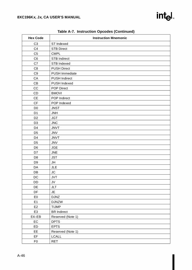
8XC196Kx, Jx, CA USER’S MANUAL
A-46
C3 ST Indexed
C4 STB Direct
C5 CMPL
C6 STB Indirect
C7 STB Indexed
C8 PUSH Direct
C9 PUSH Immediate
CA PUSH Indirect
CB PUSH Indexed
CC POP Direct
CD BMOVI
CE POP Indirect
CF POP Indexed
D0 JNST
D1 JNH
D2 JGT
D3 JNC
D4 JNVT
D5 JNV
D4 JNVT
D5 JNV
D6 JGE
D7 JNE
D8 JST
D9 JH
DA JLE
DB JC
DC JVT
DD JV
DE JLT
DF JE
E0 DJNZ
E1 DJNZW
E2 TIJMP
E3 BR Indirect
E4–EB Reserved (Note 1)
EC DPTS
ED EPTS
EE Reserved (Note 1)
EF LCALL
F0 RET
Table A-7. Instruction Opcodes (Continued)
Hex Code Instruction Mnemonic

A-47
INSTRUCTION SET REFERENCE
Table A-8 lists instructions along with their lengths and opcodes for each applicable addressingmode. A dash (—) in any column indicates “not applicable.””
F2 PUSHF
F3 POPF
F4 PUSHA
F5 POPA
F6 IDLPD
F7 TRAP
F8 CLRC
F9 SETC
FA DI
FB EI
FC CLRVT
FD NOP
FE DIV/DIVB/MUL/MULB (Note 2)
FF RST
NOTES:1. For the 8XC196KS and KT only, this opcode is reserved, but it does not generate an unimple-
mented opcode interrupt.2. Signed multiplication and division are two-byte instructions. For each signed instruction, the
first byte is “FE” and the second is the opcode of the corresponding unsigned instruction. Forexample, the opcode for MULU (3 operands) direct is “4C,” so the opcode for MUL (3 oper-ands) direct is “FE 4C.”
Table A-7. Instruction Opcodes (Continued)
Hex Code Instruction Mnemonic

8XC196Kx, Jx, CA USER’S MANUAL
A-48
Table A-8. Instruction Lengths and Hexadecimal Opcodes
Arithmetic (Group I)
Mnemonic
Direct Immediate Indirect (Note 1)
Indexed (Notes 1, 2)
Length Opcode Length Opcode Length Opcode LengthS/L Opcode
ADD (2 ops) 3 64 4 65 3 66 4/5 67
ADD (3 ops) 4 44 5 45 4 46 5/6 47
ADDB (2 ops) 3 74 3 75 3 76 4/5 77
ADDB (3 ops) 4 54 4 55 4 56 5/6 57
ADDC 3 A4 4 A5 3 A6 4/5 A7
ADDCB 3 B4 3 B5 3 B6 4/5 B7
CLR 2 01 — — — — — —
CLRB 2 11 — — — — — —
CMP 3 88 4 89 3 8A 4/5 8B
CMPB 3 98 3 99 3 9A 4/5 9B
CMPL 3 C5 — — — — — —
DEC 2 05 — — — — — —
DECB 2 15 — — — — — —
EXT 2 06 — — — — — —
EXTB 2 16 — — — — — —
INC 2 07 — — — — — —
INCB 2 17 — — — — — —
SUB (2 ops) 3 68 4 69 3 6A 4/5 6B
SUB (3 ops) 4 48 5 49 4 4A 5/6 4B
SUBB (2 ops) 3 78 3 79 3 7A 4/5 7B
SUBB (3 ops) 4 58 4 59 4 5A 5/6 5B
SUBC 3 A8 4 A9 3 AA 4/5 AB
SUBCB 3 B8 3 B9 3 BA 4/5 BB
NOTES:1. Indirect normal and indirect autoincrement share the same opcodes, as do short- and long-indexed
modes. Because word registers always have even addresses, the address can be expressed in theupper seven bits; the least-significant bit determines the addressing mode. Indirect normal and short-indexed modes make the second byte of the instruction even (LSB = 0). Indirect autoincrement andlong-indexed modes make the second byte odd (LSB = 1).
2. For indexed instructions, the first column lists instruction lengths as S/L, where S is the short-indexedinstruction length and L is the long-indexed instruction length.
3. For the SCALL and SJMP instructions, the three least-significant bits of the opcode are concatenatedwith the eight bits to form an 11-bit, 2’s complement offset.

A-49
INSTRUCTION SET REFERENCE
Arithmetic (Group II)
Mnemonic
Direct Immediate Indirect (Note 1)
Indexed (Notes 1, 2)
Length Opcode Length Opcode Length Opcode LengthS/L Opcode
DIV 4 FE 8C 5 FE 8D 4 FE 8E 5/6 FE 8F
DIVB 4 FE 9C 4 FE 9D 4 FE 9E 5/6 FE 9F
DIVU 3 8C 4 8D 3 8E 4/5 8F
DIVUB 3 9C 3 9D 3 9E 4/5 9F
MUL (2 ops) 4 FE 6C 5 FE 6D 4 FE 6E 5/6 FE 6F
MUL (3 ops) 5 FE 4C 6 FE 4D 5 FE 4E 6/7 FE 4F
MULB (2 ops) 4 FE 7C 4 FE 7D 4 FE 7E 5/6 FE 7F
MULB (3 ops) 5 FE 5C 5 FE 5D 5 FE 5E 6/7 FE 5F
MULU (2 ops) 3 6C 4 6D 3 6E 4/5 6F
MULU (3 ops) 4 4C 5 4D 4 4E 5/6 4F
MULUB (2 ops) 3 7C 3 7D 3 7E 4/5 7F
MULUB (3 ops) 4 5C 4 5D 4 5E 5/6 5F
Logical
Mnemonic
Direct Immediate Indirect (Note 1)
Indexed (Notes 1, 2)
Length Opcode Length Opcode Length Opcode LengthS/L Opcode
AND (2 ops) 3 60 4 61 3 62 4/5 63
AND (3 ops) 4 40 5 41 4 42 5/6 43
ANDB (2 ops) 3 70 3 71 3 72 4/5 73
ANDB (3 ops) 4 50 4 51 4 52 5/6 53
NEG 2 03 — — — — — —
NEGB 2 13 — — — — — —
NOT 2 02 — — — — — —
NOTB 2 12 — — — — — —
OR 3 80 4 81 3 82 4/5 83
ORB 3 90 3 91 3 92 4/5 93
XOR 3 84 4 85 3 86 4/5 87
XORB 3 94 3 95 3 96 4/5 97
Table A-8. Instruction Lengths and Hexadecimal Opcodes (Continued)
NOTES:1. Indirect normal and indirect autoincrement share the same opcodes, as do short- and long-indexed
modes. Because word registers always have even addresses, the address can be expressed in theupper seven bits; the least-significant bit determines the addressing mode. Indirect normal and short-indexed modes make the second byte of the instruction even (LSB = 0). Indirect autoincrement andlong-indexed modes make the second byte odd (LSB = 1).
2. For indexed instructions, the first column lists instruction lengths as S/L, where S is the short-indexedinstruction length and L is the long-indexed instruction length.
3. For the SCALL and SJMP instructions, the three least-significant bits of the opcode are concatenatedwith the eight bits to form an 11-bit, 2’s complement offset.

8XC196Kx, Jx, CA USER’S MANUAL
A-50
Stack
Mnemonic
Direct Immediate Indirect (Note 1)
Indexed (Notes 1, 2)
Length Opcode Length Opcode Length Opcode LengthS/L Opcode
POP 2 CC — — 2 CE 3/4 CF
POPA 1 F5 — — — — — —
POPF 1 F3 — — — — — —
PUSH 2 C8 3 C9 2 CA 3/4 CB
PUSHA 1 F4 — — — — — —
PUSHF 1 F2 — — — — — —
Data
Length Opcode Length Opcode Length Opcode Length Opcode
Mnemonic
Direct Immediate Indirect (Note 1)
Indexed (Notes 1, 2)
Length Opcode Length Opcode Length Opcode LengthS/L Opcode
BMOV — — — — 3 C1 — —
BMOVI — — — — 3 CD — —
LD 3 A0 4 A1 3 A2 4/5 A3
LDB 3 B0 3 B1 3 B2 4/5 B3
LDBSE 3 BC 3 BD 3 BE 4/5 BF
LDBZE 3 AC 3 AD 3 AE 4/5 AF
ST 3 C0 — — 3 C2 4/5 C3
STB 3 C4 — — 3 C6 4/5 C7
XCH 3 04 — — — — 4/5 0B
XCHB 3 14 — — — — 4/5 1B
Table A-8. Instruction Lengths and Hexadecimal Opcodes (Continued)
NOTES:1. Indirect normal and indirect autoincrement share the same opcodes, as do short- and long-indexed
modes. Because word registers always have even addresses, the address can be expressed in theupper seven bits; the least-significant bit determines the addressing mode. Indirect normal and short-indexed modes make the second byte of the instruction even (LSB = 0). Indirect autoincrement andlong-indexed modes make the second byte odd (LSB = 1).
2. For indexed instructions, the first column lists instruction lengths as S/L, where S is the short-indexedinstruction length and L is the long-indexed instruction length.
3. For the SCALL and SJMP instructions, the three least-significant bits of the opcode are concatenatedwith the eight bits to form an 11-bit, 2’s complement offset.

A-51
INSTRUCTION SET REFERENCE
Jump
Length Opcode Length Opcode Length Opcode Length Opcode
Mnemonic
Direct Immediate Indirect (Note 1)
Indexed (Notes 1, 2)
Length Opcode Length Opcode Length Opcode LengthS/L Opcode
BR — — — — 2 E3 — —
LJMP — — — — — — —/3 E7
SJMP (Note 3) — — — — — — 2/— 20–27
TIJMP 4 E2 4 E2 — — —/4 E2
Call
Length Opcode Length Opcode Length Opcode Length Opcode
MnemonicDirect Immediate Indirect
(Note 1)Indexed (Note 1)
Length Opcode Length Opcode Length Opcode Length Opcode
LCALL — — — — — — 3 EF
RET — — — — 1 F0 — —
SCALL (Note 3) — — — — — — 2 28–2F
TRAP 1 F7 — — — — — —
Table A-8. Instruction Lengths and Hexadecimal Opcodes (Continued)
NOTES:1. Indirect normal and indirect autoincrement share the same opcodes, as do short- and long-indexed
modes. Because word registers always have even addresses, the address can be expressed in theupper seven bits; the least-significant bit determines the addressing mode. Indirect normal and short-indexed modes make the second byte of the instruction even (LSB = 0). Indirect autoincrement andlong-indexed modes make the second byte odd (LSB = 1).
2. For indexed instructions, the first column lists instruction lengths as S/L, where S is the short-indexedinstruction length and L is the long-indexed instruction length.
3. For the SCALL and SJMP instructions, the three least-significant bits of the opcode are concatenatedwith the eight bits to form an 11-bit, 2’s complement offset.

8XC196Kx, Jx, CA USER’S MANUAL
A-52
Conditional Jump
Mnemonic
Direct Immediate Indirect Indexed (Notes 1, 2)
Length Opcode Length Opcode Length Opcode LengthS/L Opcode
DJNZ — — — — — — 3/— E0
DJNZW — — — — — — 3/— E1
JBC — — — — — — 3/— 30–37
JBS — — — — — — 3/— 38–3F
JC — — — — — — 2/— DB
JE — — — — — — 2/— DF
JGE — — — — — — 2/— D6
JGT — — — — — — 2/— D2
JH — — — — — — 2/— D9
JLE — — — — — — 2/— DA
JLT — — — — — — 2/— DE
JNC — — — — — — 2/— D3
JNE — — — — — — 2/— D7
JNH — — — — — — 2/— D1
JNST — — — — — — 2/— D0
JNV — — — — — — 2/— D5
JNVT — — — — — — 2/— D4
JST — — — — — — 2/— D8
JV — — — — — — 2/— DD
JVT — — — — — — 2/— DC
Table A-8. Instruction Lengths and Hexadecimal Opcodes (Continued)
NOTES:1. Indirect normal and indirect autoincrement share the same opcodes, as do short- and long-indexed
modes. Because word registers always have even addresses, the address can be expressed in theupper seven bits; the least-significant bit determines the addressing mode. Indirect normal and short-indexed modes make the second byte of the instruction even (LSB = 0). Indirect autoincrement andlong-indexed modes make the second byte odd (LSB = 1).
2. For indexed instructions, the first column lists instruction lengths as S/L, where S is the short-indexedinstruction length and L is the long-indexed instruction length.
3. For the SCALL and SJMP instructions, the three least-significant bits of the opcode are concatenatedwith the eight bits to form an 11-bit, 2’s complement offset.

A-53
INSTRUCTION SET REFERENCE
Shift
MnemonicDirect Immediate Indirect Indexed
Length Opcode Length Opcode Length Opcode Length Opcode
NORML 3 0F — — — — — —
SHL 3 09 — — — — — —
SHLB 3 19 — — — — — —
SHLL 3 0D — — — — — —
SHR 3 08 — — — — — —
SHRA 3 0A — — — — — —
SHRAB 3 1A — — — — — —
SHRAL 3 0E — — — — — —
SHRB 3 18 — — — — — —
SHRL 3 0C — — — — — —
Special
MnemonicDirect Immediate Indirect Indexed
Length Opcode Length Opcode Length Opcode Length Opcode
CLRC 1 F8 — — — — — —
CLRVT 1 FC — — — — — —
DI 1 FA — — — — — —
EI 1 FB — — — — — —
IDLPD — — 1 F6 — — — —
NOP 1 FD — — — — — —
RST 1 FF — — — — — —
SETC 1 F9 — — — — — —
SKIP 2 00 — — — — — —
PTS
MnemonicDirect Immediate Indirect Indexed
Length Opcode Length Opcode Length Opcode Length Opcode
DPTS 1 EC — — — — — —
EPTS 1 ED — — — — — —
Table A-8. Instruction Lengths and Hexadecimal Opcodes (Continued)
NOTES:1. Indirect normal and indirect autoincrement share the same opcodes, as do short- and long-indexed
modes. Because word registers always have even addresses, the address can be expressed in theupper seven bits; the least-significant bit determines the addressing mode. Indirect normal and short-indexed modes make the second byte of the instruction even (LSB = 0). Indirect autoincrement andlong-indexed modes make the second byte odd (LSB = 1).
2. For indexed instructions, the first column lists instruction lengths as S/L, where S is the short-indexedinstruction length and L is the long-indexed instruction length.
3. For the SCALL and SJMP instructions, the three least-significant bits of the opcode are concatenatedwith the eight bits to form an 11-bit, 2’s complement offset.

8XC196Kx, Jx, CA USER’S MANUAL
A-54
Table A-9 lists instructions alphabetically within groups, along with their execution times, ex-pressed in state times.
Table A-9. Instruction Execution Times (in State Times)
Arithmetic (Group I)
Mnemonic Direct Immed.
Indirect Indexed
Normal Autoinc. Short Long
Reg. Mem. Reg. Mem. Reg. Mem. Reg. Mem.
ADD (2 ops) 4 5 6 8 7 9 6 8 7 9
ADD (3 ops) 5 6 7 10 8 11 7 10 8 11
ADDB (2 ops) 4 4 6 8 7 9 6 8 7 9
ADDB (3 ops) 5 5 7 10 8 11 7 10 8 11
ADDC 4 5 6 8 7 9 6 8 7 9
ADDCB 4 4 6 8 7 9 6 8 7 9
CLR 3 — — — — —
CLRB 3 — — — — —
CMP 4 5 6 8 7 9 6 8 7 9
CMPB 4 4 6 8 7 9 6 8 7 9
CMPL 7 — — — — —
DEC 3 — — — — —
DECB 3 — — — — —
EXT 4 — — — — —
EXTB 4 — — — — —
INC 3 — — — — —
INCB 3 — — — — —
SUB (2 ops) 4 5 6 8 7 9 6 8 7 9
SUB (3 ops) 5 6 7 10 8 11 7 10 8 11
SUBB (2 ops) 4 4 6 8 7 9 6 8 7 9
SUBB (3 ops) 5 5 7 10 8 11 7 10 8 11
SUBC 4 5 6 8 7 9 6 8 7 9
SUBCB 4 4 6 8 7 9 6 8 7 9
NOTE: The column entitled “Reg.” lists the instruction execution times for accesses to the register file orperipheral SFRs. The column entitled “Mem.” lists the instruction execution times for accesses toall memory-mapped registers, I/O, or memory. See Table 4-1 on page 4-2 for address information.
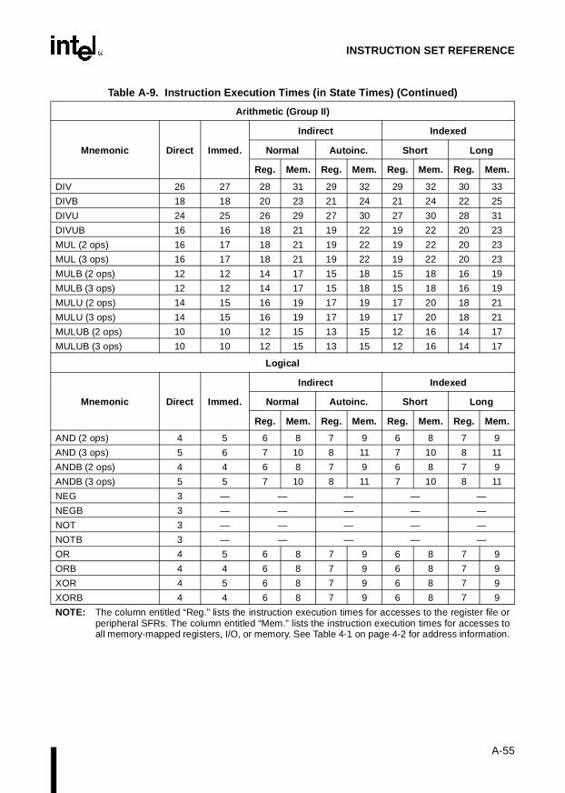
A-55
INSTRUCTION SET REFERENCE
Arithmetic (Group II)
Mnemonic Direct Immed.
Indirect Indexed
Normal Autoinc. Short Long
Reg. Mem. Reg. Mem. Reg. Mem. Reg. Mem.
DIV 26 27 28 31 29 32 29 32 30 33
DIVB 18 18 20 23 21 24 21 24 22 25
DIVU 24 25 26 29 27 30 27 30 28 31
DIVUB 16 16 18 21 19 22 19 22 20 23
MUL (2 ops) 16 17 18 21 19 22 19 22 20 23
MUL (3 ops) 16 17 18 21 19 22 19 22 20 23
MULB (2 ops) 12 12 14 17 15 18 15 18 16 19
MULB (3 ops) 12 12 14 17 15 18 15 18 16 19
MULU (2 ops) 14 15 16 19 17 19 17 20 18 21
MULU (3 ops) 14 15 16 19 17 19 17 20 18 21
MULUB (2 ops) 10 10 12 15 13 15 12 16 14 17
MULUB (3 ops) 10 10 12 15 13 15 12 16 14 17
Logical
Mnemonic Direct Immed.
Indirect Indexed
Normal Autoinc. Short Long
Reg. Mem. Reg. Mem. Reg. Mem. Reg. Mem.
AND (2 ops) 4 5 6 8 7 9 6 8 7 9
AND (3 ops) 5 6 7 10 8 11 7 10 8 11
ANDB (2 ops) 4 4 6 8 7 9 6 8 7 9
ANDB (3 ops) 5 5 7 10 8 11 7 10 8 11
NEG 3 — — — — —
NEGB 3 — — — — —
NOT 3 — — — — —
NOTB 3 — — — — —
OR 4 5 6 8 7 9 6 8 7 9
ORB 4 4 6 8 7 9 6 8 7 9
XOR 4 5 6 8 7 9 6 8 7 9
XORB 4 4 6 8 7 9 6 8 7 9
Table A-9. Instruct ion Execution Times (in State Times) (Continued)
NOTE: The column entitled “Reg.” lists the instruction execution times for accesses to the register file orperipheral SFRs. The column entitled “Mem.” lists the instruction execution times for accesses toall memory-mapped registers, I/O, or memory. See Table 4-1 on page 4-2 for address information.
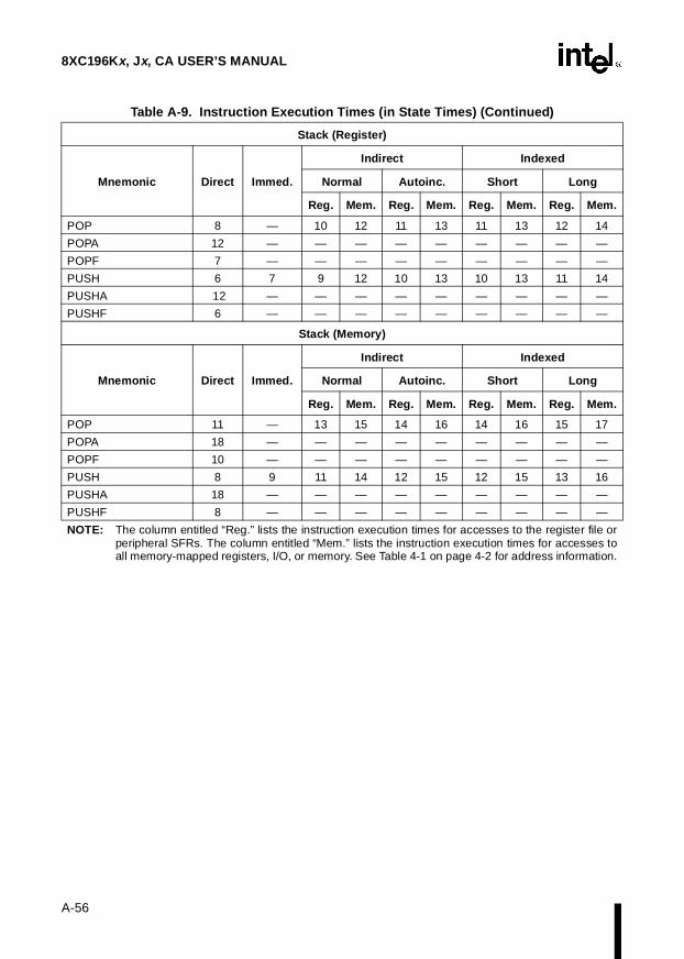
8XC196Kx, Jx, CA USER’S MANUAL
A-56
Stack (Register)
Mnemonic Direct Immed.
Indirect Indexed
Normal Autoinc. Short Long
Reg. Mem. Reg. Mem. Reg. Mem. Reg. Mem.
POP 8 — 10 12 11 13 11 13 12 14
POPA 12 — — — — — — — — —
POPF 7 — — — — — — — — —
PUSH 6 7 9 12 10 13 10 13 11 14
PUSHA 12 — — — — — — — — —
PUSHF 6 — — — — — — — — —
Stack (Memory)
Mnemonic Direct Immed.
Indirect Indexed
Normal Autoinc. Short Long
Reg. Mem. Reg. Mem. Reg. Mem. Reg. Mem.
POP 11 — 13 15 14 16 14 16 15 17
POPA 18 — — — — — — — — —
POPF 10 — — — — — — — — —
PUSH 8 9 11 14 12 15 12 15 13 16
PUSHA 18 — — — — — — — — —
PUSHF 8 — — — — — — — — —
Table A-9. Instruct ion Execution Times (in State Times) (Continued)
NOTE: The column entitled “Reg.” lists the instruction execution times for accesses to the register file orperipheral SFRs. The column entitled “Mem.” lists the instruction execution times for accesses toall memory-mapped registers, I/O, or memory. See Table 4-1 on page 4-2 for address information.
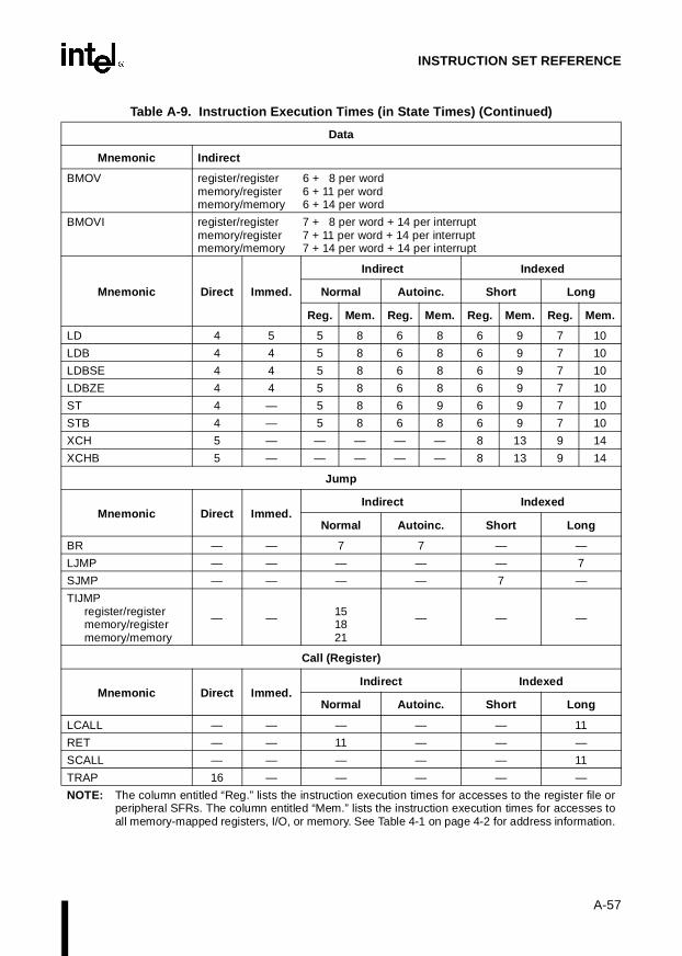
A-57
INSTRUCTION SET REFERENCE
Data
Mnemonic Indirect
BMOV register/register 6 + 8 per wordmemory/register 6 + 11 per wordmemory/memory 6 + 14 per word
BMOVI register/register 7 + 8 per word + 14 per interruptmemory/register 7 + 11 per word + 14 per interruptmemory/memory 7 + 14 per word + 14 per interrupt
Mnemonic Direct Immed.
Indirect Indexed
Normal Autoinc. Short Long
Reg. Mem. Reg. Mem. Reg. Mem. Reg. Mem.
LD 4 5 5 8 6 8 6 9 7 10
LDB 4 4 5 8 6 8 6 9 7 10
LDBSE 4 4 5 8 6 8 6 9 7 10
LDBZE 4 4 5 8 6 8 6 9 7 10
ST 4 — 5 8 6 9 6 9 7 10
STB 4 — 5 8 6 8 6 9 7 10
XCH 5 — — — — — 8 13 9 14
XCHB 5 — — — — — 8 13 9 14
Jump
Mnemonic Direct Immed. Indirect Indexed
Normal Autoinc. Short Long
BR — — 7 7 — —
LJMP — — — — — 7
SJMP — — — — 7 —
TIJMPregister/registermemory/registermemory/memory
— — 151821
— — —
Call (Register)
Mnemonic Direct Immed.Indirect Indexed
Normal Autoinc. Short Long
LCALL — — — — — 11
RET — — 11 — — —
SCALL — — — — — 11
TRAP 16 — — — — —
Table A-9. Instruct ion Execution Times (in State Times) (Continued)
NOTE: The column entitled “Reg.” lists the instruction execution times for accesses to the register file orperipheral SFRs. The column entitled “Mem.” lists the instruction execution times for accesses toall memory-mapped registers, I/O, or memory. See Table 4-1 on page 4-2 for address information.

8XC196Kx, Jx, CA USER’S MANUAL
A-58
Call (Memory)
Mnemonic Direct Immed.
Indirect Indexed
Normal Autoinc. Short Long
LCALL — — — — — 13
RET— — 14 — —
—
SCALL — — — — — 13
TRAP 18 — — — — —
Conditional Jump
Mnemonic Short-Indexed
DJNZ 5 (jump not taken), 9 (jump taken)
DJNZW 6 (jump not taken), 10 (jump taken)
JBC 5 (jump not taken), 9 (jump taken)
JBS 5 (jump not taken), 9 (jump taken)
JC 4 (jump not taken), 8 (jump taken)
JE 4 (jump not taken), 8 (jump taken)
JGE 4 (jump not taken), 8 (jump taken)
JGT 4 (jump not taken), 8 (jump taken)
JH 4 (jump not taken), 8 (jump taken)
JLE 4 (jump not taken), 8 (jump taken)
JLT 4 (jump not taken), 8 (jump taken)
JNC 4 (jump not taken), 8 (jump taken)
JNE 4 (jump not taken), 8 (jump taken)
JNH 4 (jump not taken), 8 (jump taken)
JNST 4 (jump not taken), 8 (jump taken)
JNV 4 (jump not taken), 8 (jump taken)
JNVT 4 (jump not taken), 8 (jump taken)
JST 4 (jump not taken), 8 (jump taken)
JV 4 (jump not taken), 8 (jump taken)
JVT 4 (jump not taken), 8 (jump taken)
Table A-9. Instruct ion Execution Times (in State Times) (Continued)
NOTE: The column entitled “Reg.” lists the instruction execution times for accesses to the register file orperipheral SFRs. The column entitled “Mem.” lists the instruction execution times for accesses toall memory-mapped registers, I/O, or memory. See Table 4-1 on page 4-2 for address information.

A-59
INSTRUCTION SET REFERENCE
Shift
Mnemonic Direct
NORML 8 + 1 per shift (9 for 0 shift)
SHL 6 + 1 per shift (7 for 0 shift)
SHLB 6 + 1 per shift (7 for 0 shift)
SHLL 7 + 1 per shift (8 for 0 shift)
SHR 6 + 1 per shift (7 for 0 shift)
SHRA 6 + 1 per shift (7 for 0 shift)
SHRAB 6 + 1 per shift (7 for 0 shift)
SHRAL 7 + 1 per shift (8 for 0 shift)
SHRB 6 + 1 per shift (7 for 0 shift)
SHRL 7 + 1 per shift (8 for 0 shift)
Special
Mnemonic Direct Immed. Indirect Indexed
Normal Autoinc. Short Long
CLRC 2 — — — — —
CLRVT 2 — — — — —
DI 2 — — — — —
EI 2 — — — — —
IDLPDValid keyInvalid key
——
1228
——
——
——
——
NOP 2 — — — — —
RST 4 — — — — —
SETC 2 — — — — —
SKIP 3 — — — — —
PTS
Mnemonic Direct Immed. Indirect Indexed
Normal Autoinc. Short Long
DPTS 2 — — — — —
EPTS 2 — — — — —
Table A-9. Instruct ion Execution Times (in State Times) (Continued)
NOTE: The column entitled “Reg.” lists the instruction execution times for accesses to the register file orperipheral SFRs. The column entitled “Mem.” lists the instruction execution times for accesses toall memory-mapped registers, I/O, or memory. See Table 4-1 on page 4-2 for address information.

BSignal Descriptions

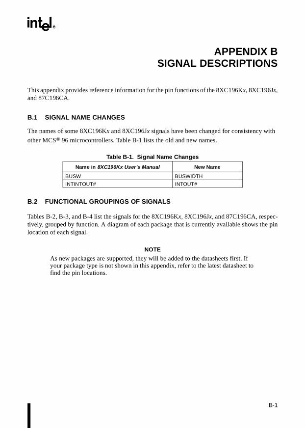
B-1
APPENDIX BSIGNAL DESCRIPTIONS
This appendix provides reference information for the pin functions of the 8XC196Kx, 8XC196Jx,and 87C196CA.
B.1 SIGNAL NAME CHANGES
The names of some 8XC196Kx and 8XC196Jx signals have been changed for consistency with
other MCS® 96 microcontrollers. Table B-1 lists the old and new names.
B.2 FUNCTIONAL GROUPINGS OF SIGNALS
Tables B-2, B-3, and B-4 list the signals for the 8XC196Kx, 8XC196Jx, and 87C196CA, respec-tively, grouped by function. A diagram of each package that is currently available shows the pinlocation of each signal.
NOTE
As new packages are supported, they will be added to the datasheets first. If your package type is not shown in this appendix, refer to the latest datasheet to find the pin locations.
Table B-1. Signal Name Ch anges
Name in 8XC196Kx User’s Manual New Name
BUSW BUSWIDTH
INTINTOUT# INTOUT#
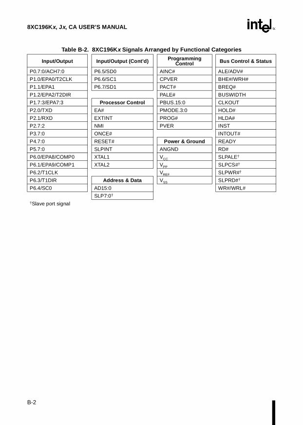
8XC196Kx, Jx, CA USER’S MANUAL
B-2
Table B-2. 8XC196Kx Signals Arranged by Functional Categories
Input/Output Input/Output (Cont’d) Programming Control Bus Control & Status
P0.7:0/ACH7:0 P6.5/SD0 AINC# ALE/ADV#
P1.0/EPA0/T2CLK P6.6/SC1 CPVER BHE#/WRH#
P1.1/EPA1 P6.7/SD1 PACT# BREQ#
P1.2/EPA2/T2DIR PALE# BUSWIDTH
P1.7:3/EPA7:3 Processor Control PBUS.15:0 CLKOUT
P2.0/TXD EA# PMODE.3:0 HOLD#
P2.1/RXD EXTINT PROG# HLDA#
P2.7:2 NMI PVER INST
P3.7:0 ONCE# INTOUT#
P4.7:0 RESET# Power & Ground READY
P5.7:0 SLPINT ANGND RD#
P6.0/EPA8/COMP0 XTAL1 VCC SLPALE†
P6.1/EPA9/COMP1 XTAL2 VPP SLPCS#†
P6.2/T1CLK VREF SLPWR#†
P6.3/T1DIR Address & Data VSS SLPRD#†
P6.4/SC0 AD15:0 WR#/WRL#
SLP7:0†
†Slave port signal
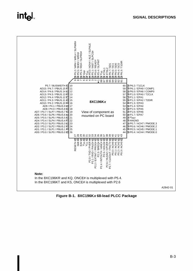
B-3
SIGNAL DESCRIPTIONS
Figure B-1. 8XC196Kx 68-lead PLCC Package
P6.2 / T1CLK P6.1 / EPA9 / COMP1 P6.0 / EPA8 / COMP0 P1.0 / EPA0 / T2CLK P1.1 / EPA1 P1.2 / EPA2 / T2DIR P1.3 / EPA3 P1.4 / EPA4 P1.5 / EPA5 P1.6 / EPA6 P1.7 / EPA7 VREF ANGND P0.7 / ACH7 / PMODE.3 P0.6 / ACH6 / PMODE.2 P0.5 / ACH5 / PMODE.1 P0.4 / ACH4 / PMODE.0
P5.
2 / W
R#
/ WR
L# /
SLP
WR
# P
5.5
/ BH
E#
/ WR
H#
P5.
3 / R
D#
/ SLP
RD
#
VP
P
VS
S
P5.
0 / A
DV
# / A
LE /
SLP
ALE
P
5.1
/ IN
ST
/ S
LPC
S#
P5.
6 / R
EA
DY
P
5.4
/ SLP
INT
V
SS
X
TA
L1
XT
AL2
P
6.7
/ SD
1 P
6.6
/ SC
1 P
6.5
/ SD
0 P
6.4
/ SC
0 P
6.3
/ T1D
IR
A2842-01
P5.7 / BUSWIDTH AD15 / P4.7 / PBUS.15 AD14 / P4.6 / PBUS.14 AD13 / P4.5 / PBUS.13 AD12 / P4.4 / PBUS.12 AD11 / P4.3 / PBUS.11 AD10 / P4.2 / PBUS.10
AD9 / P4.1 / PBUS.9 AD8 / P4.0 / PBUS.8
AD7 / P3.7 / SLP7 / PBUS.7 AD6 / P3.6 / SLP6 / PBUS.6 AD5 / P3.5 / SLP5 / PBUS.5 AD4 / P3.4 / SLP4 / PBUS.4 AD3 / P3.3 / SLP3 / PBUS.3 AD2 / P3.2 / SLP2 / PBUS.2 AD1 / P3.1 / SLP1 / PBUS.1 AD0 / P3.0 / SLP0 / PBUS.0
60 59 58 57 56 55 54 53 52 51 50 49 48 47 46 45 44
8XC196Kx
View of component as mounted on PC board
10 11 12 13 14 15 16 17 18 19 20 21 22 23 24 25 26
RE
SE
T#
NM
I E
A#
VS
S
VC
C
P2.
0 / T
XD
/ P
VE
R
P2.
1 / R
XD
/ P
ALE
# P
2.2
/ EX
TIN
T /
PR
OG
# P
2.3
/ BR
EQ
# P
2.4
/ IN
TO
UT
# / A
INC
# P
2.5
/ HO
LD#
P2.
6 / H
LDA
# / C
PV
ER
P
2.7
/ CLK
OU
T /
PA
CT
# P
0.0
/ AC
H0
P0.
1 / A
CH
1 P
0.2
/ AC
H2
P0.
3 / A
CH
3
27
28
29
30
31
32
33
34
35
36
37
38
39
40
41
42
43
9 8 7 6 5 4 3 2 1 68
67
66
65
64
63
62
61
Note: In the 8XC196KR and KQ, ONCE# is multiplexed with P5.4. In the 8XC196KT and KS, ONCE# is multiplexed with P2.6
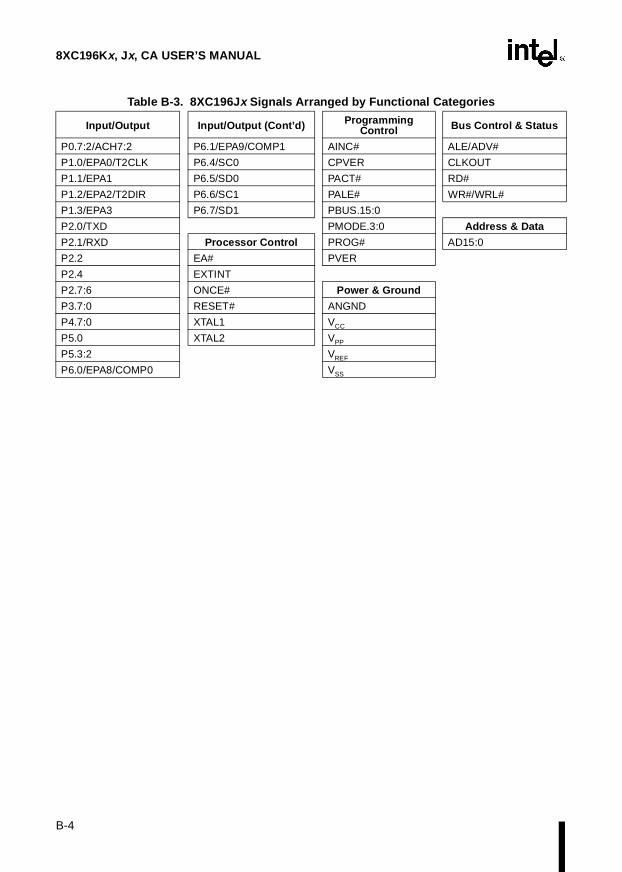
8XC196Kx, Jx, CA USER’S MANUAL
B-4
Table B-3. 8XC196J x Signals Arranged by Functional Categories
Input/Output Input/Output (Cont’d) Programming Control Bus Control & Status
P0.7:2/ACH7:2 P6.1/EPA9/COMP1 AINC# ALE/ADV#
P1.0/EPA0/T2CLK P6.4/SC0 CPVER CLKOUT
P1.1/EPA1 P6.5/SD0 PACT# RD#
P1.2/EPA2/T2DIR P6.6/SC1 PALE# WR#/WRL#
P1.3/EPA3 P6.7/SD1 PBUS.15:0
P2.0/TXD PMODE.3:0 Address & Data
P2.1/RXD Processor Control PROG# AD15:0
P2.2 EA# PVER
P2.4 EXTINT
P2.7:6 ONCE# Power & Ground
P3.7:0 RESET# ANGND
P4.7:0 XTAL1 VCC
P5.0 XTAL2 VPP
P5.3:2 VREF
P6.0/EPA8/COMP0 VSS

B-5
SIGNAL DESCRIPTIONS
Figure B-2. 8XC196J x 52-lead PLCC Package
P6.1 / EPA9 / COMP1 P6.0 / EPA8 / COMP0 P1.0 / EPA0 / T2CLK P1.1 / EPA1 P1.2 / EPA2 / T2DIR P1.3 / EPA3 VREF ANGND P0.7 / ACH7 / PMODE.3 P0.6 / ACH6 / PMODE.2 P0.5 / ACH5 / PMODE.1 P0.4 / ACH4 / PMODE.0 P0.3 / ACH3
AD
15 /
P4.
7 / P
BU
S.1
5 P
5.2
/ WR
# / W
RL#
P
5.3
/ RD
# V
PP
V
SS
P
5.0
/ AD
V#
/ ALE
V
SS
X
TA
L1
XT
AL2
P
6.7
/ SD
1 P
6.6
/ SC
1 P
6.5
/ SD
0 P
6.4
/ SC
0
A2843-01
AD14 / P4.6 / PBUS.14 AD13 / P4.5 / PBUS.13 AD12 / P4.4 / PBUS.12 AD11 / P4.3 / PBUS.11 AD10 / P4.2 / PBUS.10
AD9 / P4.1 / PBUS.9 AD8 / P4.0 / PBUS.8 AD7 / P3.7 / PBUS.7 AD6 / P3.6 / PBUS.6 AD5 / P3.5 / PBUS.5 AD4 / P3.4 / PBUS.4 AD3 / P3.3 / PBUS.3 AD2 / P3.2 / PBUS.2
46 45 44 43 42 41 40 39 38 37 36 35 34
8XC196Jx
View of component as mounted on PC board
8 9 10 11 12 13 14 15 16 17 18 19 20
AD
1 / P
3.1
/ PB
US
.1
AD
0 / P
3.0
/ PB
US
.0
RE
SE
T#
EA
# V
SS
V
CC
P
2.0
/ T
XD
/ P
VE
R
P2.
1 / R
XD
/ P
ALE
# P
2.2
/ EX
TIN
T /
PR
OG
# P
2.4
/ AIN
C#
P2.
6 /
ON
CE
# / C
PV
ER
P
2.7
/ CLK
OU
T /
PA
CT
# P
0.2
/ AC
H2
21
22
23
24
25
26
27
28
29
30
31
32
33
7 6 5 4 3 2 1 52
51
50
49
48
47
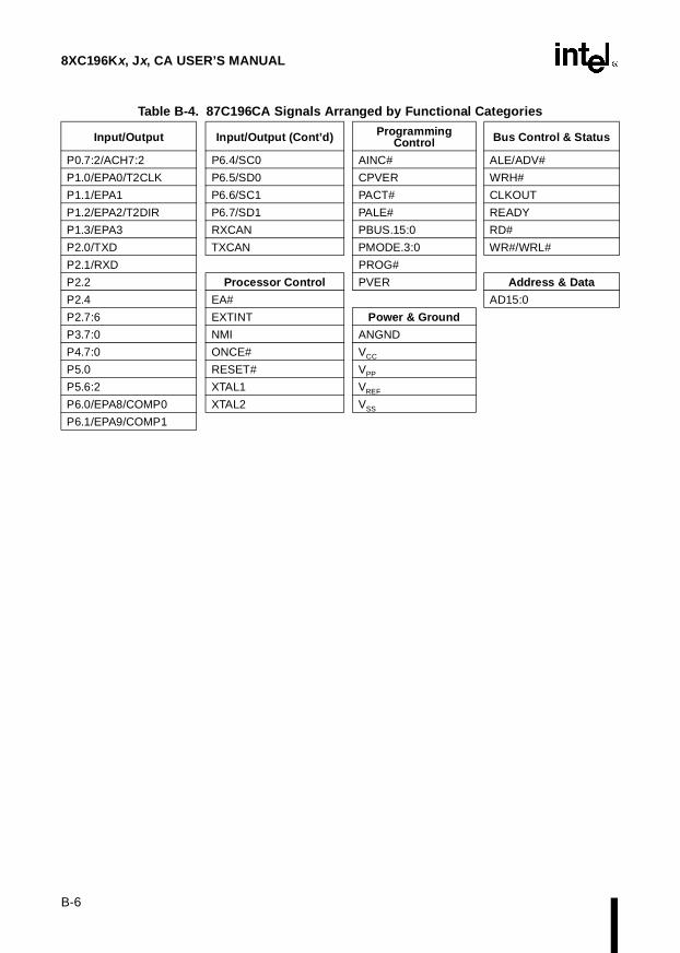
8XC196Kx, Jx, CA USER’S MANUAL
B-6
Table B-4. 87C196CA Signals Arranged by Functional Categories
Input/Output Input/Output (Cont’d) Programming Control Bus Control & Status
P0.7:2/ACH7:2 P6.4/SC0 AINC# ALE/ADV#
P1.0/EPA0/T2CLK P6.5/SD0 CPVER WRH#
P1.1/EPA1 P6.6/SC1 PACT# CLKOUT
P1.2/EPA2/T2DIR P6.7/SD1 PALE# READY
P1.3/EPA3 RXCAN PBUS.15:0 RD#
P2.0/TXD TXCAN PMODE.3:0 WR#/WRL#
P2.1/RXD PROG#
P2.2 Processor Control PVER Address & Data
P2.4 EA# AD15:0
P2.7:6 EXTINT Power & Ground
P3.7:0 NMI ANGND
P4.7:0 ONCE# VCC
P5.0 RESET# VPP
P5.6:2 XTAL1 VREF
P6.0/EPA8/COMP0 XTAL2 VSS
P6.1/EPA9/COMP1
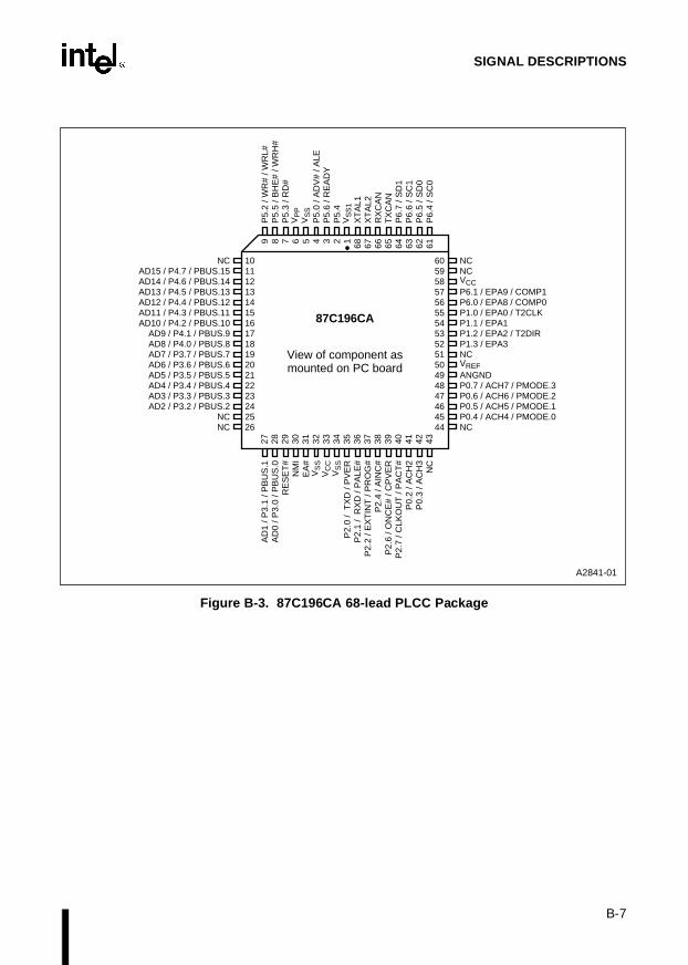
B-7
SIGNAL DESCRIPTIONS
Figure B-3. 87C196CA 68-lead PLCC Package
NC NC VCC P6.1 / EPA9 / COMP1 P6.0 / EPA8 / COMP0 P1.0 / EPA0 / T2CLK P1.1 / EPA1 P1.2 / EPA2 / T2DIR P1.3 / EPA3 NC VREF ANGND P0.7 / ACH7 / PMODE.3 P0.6 / ACH6 / PMODE.2 P0.5 / ACH5 / PMODE.1 P0.4 / ACH4 / PMODE.0 NC
P5.
2 / W
R#
/ WR
L#
P5.
5 / B
HE
# / W
RH
# P
5.3
/ RD
# V
PP
V
SS
P
5.0
/ AD
V#
/ ALE
P
5.6
/ RE
AD
Y
P5.
4 V
SS
1 X
TA
L1
XT
AL2
R
XC
AN
T
XC
AN
P
6.7
/ SD
1 P
6.6
/ SC
1 P
6.5
/ SD
0 P
6.4
/ SC
0
A2841-01
NC AD15 / P4.7 / PBUS.15 AD14 / P4.6 / PBUS.14 AD13 / P4.5 / PBUS.13 AD12 / P4.4 / PBUS.12 AD11 / P4.3 / PBUS.11 AD10 / P4.2 / PBUS.10
AD9 / P4.1 / PBUS.9 AD8 / P4.0 / PBUS.8 AD7 / P3.7 / PBUS.7 AD6 / P3.6 / PBUS.6 AD5 / P3.5 / PBUS.5 AD4 / P3.4 / PBUS.4 AD3 / P3.3 / PBUS.3 AD2 / P3.2 / PBUS.2
NC NC
60 59 58 57 56 55 54 53 52 51 50 49 48 47 46 45 44
87C196CA
View of component as mounted on PC board
10 11 12 13 14 15 16 17 18 19 20 21 22 23 24 25 26
AD
1 / P
3.1
/ PB
US
.1
AD
0 / P
3.0
/ PB
US
.0
RE
SE
T#
NM
I E
A#
VS
S
VC
C
VS
S
P2.
0 /
TX
D /
PV
ER
P
2.1
/ R
XD
/ P
ALE
# P
2.2
/ EX
TIN
T /
PR
OG
# P
2.4
/ AIN
C#
P2.
6 / O
NC
E#
/ CP
VE
R
P2.
7 / C
LKO
UT
/ P
AC
T#
P0.
2 / A
CH
2 P
0.3
/ AC
H3
NC
27
28
29
30
31
32
33
34
35
36
37
38
39
40
41
42
43
9 8 7 6 5 4 3 2 1 68
67
66
65
64
63
62
61

8XC196Kx, Jx, CA USER’S MANUAL
B-8
B.3 SIGNAL DESCRIPTIONS
Table B-5 defines the columns used in Table B-6, which describes the signals.
Table B-5. Description of Columns of Table B-6
Column Heading Description
Name Lists the signals, arranged alphabetically. Many pins have two functions, so there are more entries in this column than there are pins. Every signal is listed in this column.
Type Identifies the pin function listed in the Name column as an input (I), output (O), bidirectional (I/O), power (PWR), or ground (GND).
Note that all inputs except RESET# are sampled inputs. RESET# is a level-sensitive input. During powerdown mode, the powerdown circuitry uses EXTINT as a level-sensitive input.
Description Briefly describes the function of the pin for the specific signal listed in the Name column. Also lists the alternate fuction that are multiplexed with the signal (if applicable).
Table B-6. Signal Descriptions
Name Type Description
ACH7:0 (Kx)
ACH7:2 (CA/Jx)
I Analog Channels
These pins are analog inputs to the A/D converter.
These pins may individually be used as analog inputs (ACHx) or digital inputs (P0.x). While it is possible for the pins to function simultaneously as analog and digital inputs, this is not recommended because reading port 0 while a conversion is in process can produce unreliable conversion results.
The ANGND and VREF pins must be connected for the A/D converter and port 0 to function.
NOTE: On the 8XC196Jx and 87C196CA, ACH0 and ACH1 are tied to VREFinternally. The result of reading these channels is 3FFH (full-scale).
On the 8XC196Kx, ACH7:0 are multiplexed as follows: ACH0/P0.0, ACH1/P0.1, ACH2/P0.2, ACH3/P0.3, ACH4/P0.4/PMODE.0, ACH5/P0.5/PMODE.1, ACH6/P0.6/PMODE.2, and ACH7/P0.7/PMODE.3.
On the 8XC196Jx and 87C196CA, ACH7:2 are multiplexed as follows: ACH2/P0.2, ACH3/P0.3, ACH4/P0.4/PMODE.0, ACH5/P0.5/PMODE.1, ACH6/P0.6/PMODE.2, and ACH7/P0.7/PMODE.3.
ACH1:0 are not implemented on the 8XC196Jx and 87C196CA.†This signal is not implemented on the 8XC196Jx or 87C196CA (see “Design Considerations for 8XC196JQ, JR, JT, and JV Devices” on page 2-14 or “Design Considerations for 87C196CA Devices” on page 2-13).††This signal is not implemented on the 8XC196Jx (see “Design Considerations for 8XC196JQ, JR, JT, and JV Devices” on page 2-14).

B-9
SIGNAL DESCRIPTIONS
AD15:0 I/O Address/Data Lines
These pins provide a multiplexed address and data bus. During the address phase of the bus cycle, address bits 0–15 are presented on the bus and can be latched using ALE or ADV#. During the data phase, 8- or 16-bit data is trans-ferred.
AD7:0 are multiplexed with SLP7:0††, P3.7:0 and PBUS.7:0. AD15:8 are multiplexed with P4.7:0 and PBUS.15:8.
ADV# O Address Valid
This active-low output signal is asserted only during external memory accesses. ADV# indicates that valid address information is available on the system address/data bus. The signal remains low while a valid bus cycle is in progress and is returned high as soon as the bus cycle completes.
An external latch can use this signal to demultiplex the address from the address/data bus. A decoder can also use this signal to generate chip selects for external memory.
On the 8XC196Kx, ADV# is multiplexed with P5.0, SLPALE, and ALE.
On the 8XC196Jx and 87C196CA, ADV# is multiplexed with P5.0 and ALE.
AINC# I Auto Increment
During slave programming, this active-low input enables the auto-increment feature. (Auto increment allows reading or writing of sequential OTPROM locations, without requiring address transactions across the PBUS for each read or write.) AINC# is sampled after each location is programmed or dumped. If AINC# is asserted, the address is incremented and the next data word is programmed or dumped.
On the 8XC196Kx, AINC# is multiplexed with P2.4 and INTOUT#.
On the 8XC196Jx and 87C196CA, AINC# is multiplexed with P2.4.
ALE O Address Latch Enable
This active-high output signal is asserted only during external memory cycles. ALE signals the start of an external bus cycle and indicates that valid address information is available on the system address/data bus. ALE differs from ADV# in that it does not remain active during the entire bus cycle.
An external latch can use this signal to demultiplex the address from the address/data bus.
On the 8XC196Kx, ALE is multiplexed with P5.0, SLPALE, and ADV#.
On the 8XC196Jx and 87C196CA, ALE is multiplexed with P5.0 and ADV#.
ANGND GND Analog Ground
ANGND must be connected for A/D converter and port 0 operation. ANGND and VSS should be nominally at the same potential.
Table B-6. Signal Descriptions (Continued)
Name Type Description
†This signal is not implemented on the 8XC196Jx or 87C196CA (see “Design Considerations for 8XC196JQ, JR, JT, and JV Devices” on page 2-14 or “Design Considerations for 87C196CA Devices” on page 2-13).††This signal is not implemented on the 8XC196Jx (see “Design Considerations for 8XC196JQ, JR, JT, and JV Devices” on page 2-14).
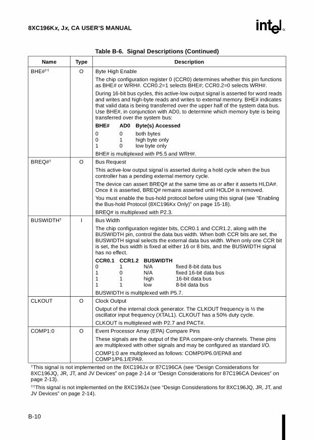
8XC196Kx, Jx, CA USER’S MANUAL
B-10
BHE#†† O Byte High Enable
The chip configuration register 0 (CCR0) determines whether this pin functions as BHE# or WRH#. CCR0.2=1 selects BHE#; CCR0.2=0 selects WRH#.
During 16-bit bus cycles, this active-low output signal is asserted for word reads and writes and high-byte reads and writes to external memory. BHE# indicates that valid data is being transferred over the upper half of the system data bus. Use BHE#, in conjunction with AD0, to determine which memory byte is being transferred over the system bus:
BHE# AD0 Byte(s) Accessed
0 0 both bytes0 1 high byte only1 0 low byte only
BHE# is multiplexed with P5.5 and WRH#.
BREQ#† O Bus Request
This active-low output signal is asserted during a hold cycle when the bus controller has a pending external memory cycle.
The device can assert BREQ# at the same time as or after it asserts HLDA#. Once it is asserted, BREQ# remains asserted until HOLD# is removed.
You must enable the bus-hold protocol before using this signal (see “Enabling the Bus-hold Protocol (8XC196Kx Only)” on page 15-18).
BREQ# is multiplexed with P2.3.
BUSWIDTH† I Bus Width
The chip configuration register bits, CCR0.1 and CCR1.2, along with the BUSWIDTH pin, control the data bus width. When both CCR bits are set, the BUSWIDTH signal selects the external data bus width. When only one CCR bit is set, the bus width is fixed at either 16 or 8 bits, and the BUSWIDTH signal has no effect.
CCR0.1 CCR1.2 BUSWIDTH0 1 N/A fixed 8-bit data bus1 0 N/A fixed 16-bit data bus1 1 high 16-bit data bus1 1 low 8-bit data bus
BUSWIDTH is multiplexed with P5.7.
CLKOUT O Clock Output
Output of the internal clock generator. The CLKOUT frequency is ½ the oscillator input frequency (XTAL1). CLKOUT has a 50% duty cycle.
CLKOUT is multiplexed with P2.7 and PACT#.
COMP1:0 O Event Processor Array (EPA) Compare Pins
These signals are the output of the EPA compare-only channels. These pins are multiplexed with other signals and may be configured as standard I/O.
COMP1:0 are multiplexed as follows: COMP0/P6.0/EPA8 and COMP1/P6.1/EPA9.
Table B-6. Signal Descriptions (Continued)
Name Type Description
†This signal is not implemented on the 8XC196Jx or 87C196CA (see “Design Considerations for 8XC196JQ, JR, JT, and JV Devices” on page 2-14 or “Design Considerations for 87C196CA Devices” on page 2-13).††This signal is not implemented on the 8XC196Jx (see “Design Considerations for 8XC196JQ, JR, JT, and JV Devices” on page 2-14).

B-11
SIGNAL DESCRIPTIONS
CPVER O Cumulative Program Verification
During slave programming, a high signal indicates that all locations programmed correctly, while a low signal indicates that an error occurred during one of the programming operations.
On the 8XC196Kx, CPVER is multiplexed with P2.6 and HLDA#.
On the 8XC196Jx and 87C196CA, CPVER is multiplexed with P2.6 and ONCE#.
EA# I External Access
EA# is sampled and latched only on the rising edge of RESET#. Changing the level of EA# after reset has no effect. Accesses to special-purpose and program memory partitions are directed to internal memory if EA# is held high and to external memory if EA# is held low. (See Table 4-1 on page 4-2 for address ranges of special-purpose and program memory partitions.)
EA# also controls program mode entry. If EA# is at VPP voltage (typically +12.5 V) on the rising edge of RESET#, the device enters programming mode.
NOTE: When EA# is active, ports 3 and 4 will function only as theaddress/data bus. They cannot be used for standard I/O.
On devices with no internal nonvolatile memory, always connect EA# to VSS.
EPA9:0 (Kx)EPA9:8, EPA3:0 (Jx, CA)
I/O Event Processor Array (EPA) Input/Output pins
These are the high-speed input/output pins for the EPA capture/compare channels. For high-speed PWM applications, the outputs of two EPA channels (either EPA0 and EPA1 or EPA2 and EPA3) can be remapped to produce a PWM waveform on a shared output pin (see “Generating a High-speed PWM Output” on page 10-16).
EPA9:0 are multiplexed as follows: EPA0/P1.0/T2CLK, EPA1/P1.1, EPA2/P1.2/T2DIR, EPA3/P1.3, EPA4/P1.4, EPA5/P1.5, EPA6/P1.6, EPA7/P1.7, EPA8/P6.0/COMP0, and EPA9/P6.1/COMP1.
EPA7:4 are not implemented on the 8XC196Jx or 87C196CA.
Table B-6. Signal Descriptions (Continued)
Name Type Description
†This signal is not implemented on the 8XC196Jx or 87C196CA (see “Design Considerations for 8XC196JQ, JR, JT, and JV Devices” on page 2-14 or “Design Considerations for 87C196CA Devices” on page 2-13).††This signal is not implemented on the 8XC196Jx (see “Design Considerations for 8XC196JQ, JR, JT, and JV Devices” on page 2-14).

8XC196Kx, Jx, CA USER’S MANUAL
B-12
EXTINT I External Interrupt
In normal operating mode, a rising edge on EXTINT sets the EXTINT interrupt pending flag. EXTINT is sampled during phase 2 (CLKOUT high). The minimum high time is one state time.
If the chip is in idle mode and if EXTINT is enabled, a rising edge on EXTINT brings the chip back to normal operation, where the first action is to execute the EXTINT service routine. After completion of the service routine, execution resumes at the the IDLPD instruction following the one that put the device into idle mode.
In powerdown mode, asserting EXTINT causes the chip to return to normal operating mode. If EXTINT is enabled, the EXTINT service routine is executed. Otherwise, execution continues at the instruction following the IDLPD instruction that put the device into powerdown mode.
EXTINT is multiplexed with P2.2 and PROG#.
HLDA#† O Bus Hold Acknowledge
This active-low output indicates that the CPU has released the bus as the result of an external device asserting HOLD#.
HLDA# is multiplexed with P2.6 and CPVER.
HOLD#† I Bus Hold Request
An external device uses this active-low input signal to request control of the bus. This pin functions as HOLD# only if the pin is configured for its special function (see “Bidirectional Port Pin Configurations” on page 6-10) and the bus-hold protocol is enabled. Setting bit 7 of the window selection register enables the bus-hold protocol.
HOLD# is multiplexed with P2.5.
INST† O Instruction Fetch
This active-high output signal is valid only during external memory bus cycles. When high, INST indicates that an instruction is being fetched from external memory. The signal remains high during the entire bus cycle of an external instruction fetch. INST is low for data accesses, including interrupt vector fetches and chip configuration byte reads. INST is low during internal memory fetches.
INST is multiplexed with P5.1 and SLPCS#.
INTOUT#† O Interrupt Output
This active-low output indicates that a pending interrupt requires use of the external bus. If the 8XC196Kx receives an interrupt request while it is in hold, the 8XC196Kx asserts INTOUT# only if it is executing from internal memory. If the 8XC196Kx needs to access external memory, it asserts BREQ# and waits until the external device deasserts HOLD# to assert INTOUT#. If the 8XC196Kx receives an interrupt request as it is going into hold (between the time that an external device asserts HOLD# and the time that the 8XC196Kx responds with HLDA#), the 8XC196Kx asserts INTOUT# and keeps it asserted until the external device deasserts HOLD#.
INTOUT is multiplexed with P2.4 and AINC#.
Table B-6. Signal Descriptions (Continued)
Name Type Description
†This signal is not implemented on the 8XC196Jx or 87C196CA (see “Design Considerations for 8XC196JQ, JR, JT, and JV Devices” on page 2-14 or “Design Considerations for 87C196CA Devices” on page 2-13).††This signal is not implemented on the 8XC196Jx (see “Design Considerations for 8XC196JQ, JR, JT, and JV Devices” on page 2-14).

B-13
SIGNAL DESCRIPTIONS
NMI†† I Nonmaskable Interrupt
In normal operating mode, a rising edge on NMI causes a vector through the NMI interrupt at location 203EH. NMI must be asserted for greater than one state time to guarantee that it is recognized.
In idle mode, a rising edge on the NMI pin causes the device to return to normal operation, where the first action is to execute the NMI service routine. After completion of the service routine, execution resumes at the instruction following the IDLPD instruction that put the device into idle mode.
In powerdown mode, a rising edge on the NMI pin does not cause the device to exit powerdown.
ONCE# I On-circuit Emulation
Holding ONCE# low during the rising edge of RESET# places the device into on-circuit emulation (ONCE) mode. This mode puts all pins into a high-impedance state, thereby isolating the device from other components in the system. The value of ONCE# is latched when the RESET# pin goes inactive. While the device is in ONCE mode, you can debug the system using a clip-on emulator. To exit ONCE mode, reset the device by pulling the RESET# signal low. To prevent inadvertent entry into ONCE mode, either configure this pin as an output or hold it high during reset and ensure that your system meets the VIH specification (see datasheet).
On the 8XC196KR and KQ, ONCE# is multiplexed with P5.4 and SLPINT.
On the 8XC196KT and KS, ONCE# is multiplexed with P2.6 and HLDA#.
On the 8XC196Jx and CA, ONCE# is multiplexed with P2.6.
P0.7:0 (Kx)
P0.7:2 (Jx, CA)
I Port 0
This is a high-impedance, input-only port. Port 0 pins should not be left floating.
These pins may individually be used as analog inputs (ACHx) or digital inputs (P0.x). While it is possible for the pins to function simultaneously as analog and digital inputs, this is not recommended because reading port 0 while a conversion is in process can produce unreliable conversion results.
ANGND and VREF must be connected for port 0 to function.
On the 8XC196Kx, P0.3:0 are multiplexed with ACH3:0 and P0.7:4 are multiplexed with ACH7:4 and PMODE.3:0.
On the 8XC196Jx and 87C196CA, P0.3:2 are multiplexed with ACH3:2 and P0.7:4 are multiplexed with ACH7:4 and PMODE.3:0.
P0.1:0 are not implemented on the 8XC196Jx and 87C196CA.
P1.7:0 (Kx)P1.3:0 (Jx, CA)
I/O Port 1
This is a standard, bidirectional port that is multiplexed with individually selectable special-function signals.
Port 1 is multiplexed as follows: P1.0/EPA0/T2CLK, P1.1/EPA1, P1.2/EPA2/T2DIR, P1.3/EPA3, P1.4/EPA4, P1.5/EPA5, P1.6/EPA6, and P1.7/EPA7.
P1.7:4 are not implemented on the 8XC196Jx and 87C196CA.
Table B-6. Signal Descriptions (Continued)
Name Type Description
†This signal is not implemented on the 8XC196Jx or 87C196CA (see “Design Considerations for 8XC196JQ, JR, JT, and JV Devices” on page 2-14 or “Design Considerations for 87C196CA Devices” on page 2-13).††This signal is not implemented on the 8XC196Jx (see “Design Considerations for 8XC196JQ, JR, JT, and JV Devices” on page 2-14).

8XC196Kx, Jx, CA USER’S MANUAL
B-14
P2.7:0 (Kx)P2.7:6, P2.4, P2.2:0 (Jx, CA)
I/O Port 2
This is a standard bidirectional port that is multiplexed with individually selectable special-function signals.
P2.6 is multiplexed with the ONCE# function (CA, JR, JT, JV, KS, KT) or a special test-mode-entry function (KR, KQ). If this pin is held low during reset, the device will enter ONCE mode or a reserved test mode, so exercise caution if you use this pin for input. If you choose to configure this pin as an input, always hold it high during reset and ensure that your system meets the VIH specification (see datasheet) to prevent inadvertent entry into ONCE mode or a test mode.
On the 8XC196Kx, port 2 is multiplexed as follows: P2.0/TXD/PVER, P2.1/RXD/PALE#, P2.2/EXTINT/PROG#, P2.3/BREQ#, P2.4/INTOUT#/AINC#, P2.5/HOLD#, P2.6/HLDA#/ONCE#(KT, KS)/CPVER, P2.7/CLKOUT/PACT#.
On the 8XC196Jx and 87C196CA, port 2 is multiplexed as follows: P2.0/TXD/PVER, P2.1/RXD/PALE#, P2.2/EXTINT/PROG#, P2.4/AINC#, P2.6/ONCE#/CPVER, P2.7/CLKOUT/PACT#. P2.3 and P2.5 are not imple-mented.
P3.7:0 I/O Port 3
This is an 8-bit, bidirectional, memory-mapped I/O port with open-drain outputs. The pins are shared with the multiplexed address/data bus, which has comple-mentary drivers.
P3.7:0 are multiplexed with AD7:0, SLP7:0 (Kx only), and PBUS.7:0.
P4.7:0 I/O Port 4
This is an 8-bit, bidirectional, memory-mapped I/O port with open-drain outputs.
P4.7:0 are multiplexed with AD15:8 and PBUS15:8.
P5.7:0 I/O Port 5
This is an 8-bit, bidirectional, memory-mapped I/O port.
P5.4 is multiplexed with the ONCE# function (KR, KQ) or a special test-mode-entry function (CA, KS, KT). If this pin is held low during reset, the device will enter ONCE mode or a reserved test mode, so exercise caution if you use this pin for input. If you choose to configure this pin as an input, always hold it high during reset and ensure that your system meets the VIH specification (see datasheet) to prevent inadvertent entry into ONCE mode or a test mode.
On the 8XC196Kx, port 5 is multiplexed as follows: P5.0/ALE/ADV#/SLPALE, P5.1/INST/SLPCS#, P5.2/WR#/WRL#/SLPWR#, P5.3/RD#/SLPRD#, P5.4/ONCE# (KR, KQ)/SLPINT, P5.5/BHE#/WRH#, P5.6/READY, and P5.7/BUSWIDTH.
On the 8XC196Jx, port 5 is multiplexed as follows: P5.0/ADV#/ALE, P5.2/WR#/WRL#, and P5.3/RD#. P5.1 and P5.7:4 are not implemented.
On the 87C196CA, port 5 is multiplexed as follows: P5.0/ADV#/ALE, P5.2/WR#/WRL#, P5.3/RD#, P5.5/BHE#/WRH#, and P5.6/READY. P5.4 is not multiplexed; P5.1 and P5.7 are not implemented.
Table B-6. Signal Descriptions (Continued)
Name Type Description
†This signal is not implemented on the 8XC196Jx or 87C196CA (see “Design Considerations for 8XC196JQ, JR, JT, and JV Devices” on page 2-14 or “Design Considerations for 87C196CA Devices” on page 2-13).††This signal is not implemented on the 8XC196Jx (see “Design Considerations for 8XC196JQ, JR, JT, and JV Devices” on page 2-14).

B-15
SIGNAL DESCRIPTIONS
P6.7:0 I/O Port 6
This is a standard 8-bit bidirectional port.
Port 6 is multiplexed as follows: P6.0/EPA8/COMP0, P6.1/EPA9/COMP1, P6.2/T1CLK, P6.3/T1DIR, P6.4/SC0, P6.5/SD0, P6.6/SC1, and P6.7/SD1.
P6.2 and P6.3 are not implemented on the 8XC196Jx and 87C196CA.
PACT# O Programming Active
During auto programming or ROM-dump, a low signal indicates that programming or dumping is in progress, while a high signal indicates that the operation is complete.
PACT# is multiplexed with P2.7 and CLKOUT.
PALE# I Programming ALE
During slave programming, a falling edge causes the device to read a command and address from the PBUS.
PALE# is multiplexed with P2.1 and RXD.
PBUS.15:0 I/O Address/Command/Data Bus
During slave programming, ports 3 and 4 serve as a bidirectional port with open-drain outputs to pass commands, addresses, and data to or from the device. Slave programming requires external pull-up resistors.
During auto programming and ROM-dump, ports 3 and 4 serve as a regular system bus to access external memory. P4.6 and P4.7 are left unconnected; P1.1 and P1.2 serve as the upper address lines.
Slave programming:
PBUS.7:0 are multiplexed with AD7:0, SLP7:0 (Kx only), and P3.7:0.
PBUS.15:8 are multiplexed with AD15:8 and P4.7:0.
Auto programming:
PBUS.7:0 are multiplexed with AD7:0, SLP7:0 (Kx only), and P3.7:0.
PBUS.13:8 are multiplexed with AD13:8 and P4.5:0; PBUS15:14 are multiplexed with P1.2:1.
PMODE.3:0 I Programming Mode Select
Determines the programming mode. PMODE is sampled after a device reset and must be static while the part is operating. (Table 16-7 on page 16-14 lists the PMODE values and programming modes.)
PMODE.3:0 are multiplexed with P0.7:4 and ACH7:4.
PROG# I Programming Start
During programming, a falling edge latches data on the PBUS and begins programming, while a rising edge ends programming. The current location is programmed with the same data as long as PROG# remains asserted, so the data on the PBUS must remain stable while PROG# is active.
During a word dump, a falling edge causes the contents of an OTPROM location to be output on the PBUS, while a rising edge ends the data transfer.
PROG# is multiplexed with P2.2 and EXTINT.
Table B-6. Signal Descriptions (Continued)
Name Type Description
†This signal is not implemented on the 8XC196Jx or 87C196CA (see “Design Considerations for 8XC196JQ, JR, JT, and JV Devices” on page 2-14 or “Design Considerations for 87C196CA Devices” on page 2-13).††This signal is not implemented on the 8XC196Jx (see “Design Considerations for 8XC196JQ, JR, JT, and JV Devices” on page 2-14).
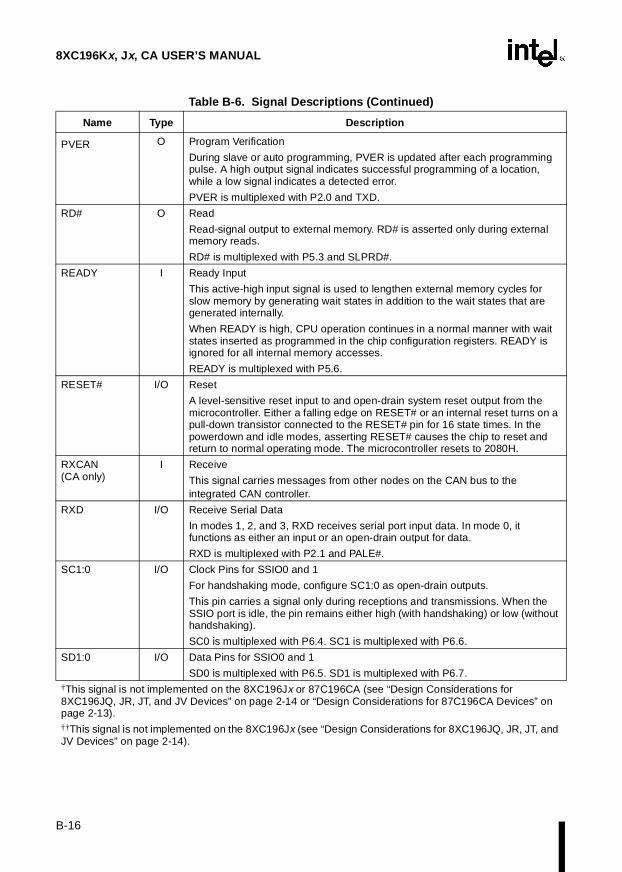
8XC196Kx, Jx, CA USER’S MANUAL
B-16
PVER O Program Verification
During slave or auto programming, PVER is updated after each programming pulse. A high output signal indicates successful programming of a location, while a low signal indicates a detected error.
PVER is multiplexed with P2.0 and TXD.
RD# O Read
Read-signal output to external memory. RD# is asserted only during external memory reads.
RD# is multiplexed with P5.3 and SLPRD#.
READY I Ready Input
This active-high input signal is used to lengthen external memory cycles for slow memory by generating wait states in addition to the wait states that are generated internally.
When READY is high, CPU operation continues in a normal manner with wait states inserted as programmed in the chip configuration registers. READY is ignored for all internal memory accesses.
READY is multiplexed with P5.6.
RESET# I/O Reset
A level-sensitive reset input to and open-drain system reset output from the microcontroller. Either a falling edge on RESET# or an internal reset turns on a pull-down transistor connected to the RESET# pin for 16 state times. In the powerdown and idle modes, asserting RESET# causes the chip to reset and return to normal operating mode. The microcontroller resets to 2080H.
RXCAN(CA only)
I Receive
This signal carries messages from other nodes on the CAN bus to the integrated CAN controller.
RXD I/O Receive Serial Data
In modes 1, 2, and 3, RXD receives serial port input data. In mode 0, it functions as either an input or an open-drain output for data.
RXD is multiplexed with P2.1 and PALE#.
SC1:0 I/O Clock Pins for SSIO0 and 1
For handshaking mode, configure SC1:0 as open-drain outputs.
This pin carries a signal only during receptions and transmissions. When the SSIO port is idle, the pin remains either high (with handshaking) or low (without handshaking).
SC0 is multiplexed with P6.4. SC1 is multiplexed with P6.6.
SD1:0 I/O Data Pins for SSIO0 and 1
SD0 is multiplexed with P6.5. SD1 is multiplexed with P6.7.
Table B-6. Signal Descriptions (Continued)
Name Type Description
†This signal is not implemented on the 8XC196Jx or 87C196CA (see “Design Considerations for 8XC196JQ, JR, JT, and JV Devices” on page 2-14 or “Design Considerations for 87C196CA Devices” on page 2-13).††This signal is not implemented on the 8XC196Jx (see “Design Considerations for 8XC196JQ, JR, JT, and JV Devices” on page 2-14).

B-17
SIGNAL DESCRIPTIONS
SLP7:0† I/O Slave Port Address/Data bus
Slave port address/data bus in multiplexed mode and slave port data bus in demultiplexed mode. In multiplexed mode, SLP1 is the source of the internal control signal, SLP_ADDR.
SLP7:0 are multiplexed with AD7:0, P3.7:0, and PBUS.7:0.
SLPALE† I Slave Port Address Latch Enable
Functions as either a latch enable input to latch the value on SLP1 (with a multiplexed address/data bus) or as the source of the internal control signal, SLP_ADDR (with a demultiplexed address/data bus).
SLPALE is multiplexed with P5.0, ADV#, and ALE.
SLPCS#† I Slave Port Chip Select
SLPCS# must be held low to enable slave port operation.
SLPCS# is multiplexed with P5.1 and INST.
SLPINT† O Slave Port Interrupt
This active-high slave port output signal can be used to interrupt the master processor.
SLPINT is multiplexed with P5.4 and the ONCE# function (KR, KQ) or a special test-mode-entry pin (KS, KT). See P5.7:0 for special considerations.
SLPRD#† I Slave Port Read Control Input
This active-low signal is an input to the slave. Data from the P3_REG or SLP_STAT register is valid after the falling edge of SLPRD#.
SLPRD# is multiplexed with P5.3 and RD#.
SLPWR#† I Slave Port Write Control Input
This active-low signal is an input to the slave. The rising edge of SLPWR# latches data on port 3 into the P3_PIN or SLP_CMD register.
SLPWR# is multiplexed with P5.2, WR#, and WRL#.
T1CLK† I Timer 1 External Clock
External clock for timer 1. Timer 1 increments (or decrements) on both rising and falling edges of T1CLK. Also used in conjunction with T1DIR for quadrature counting mode.
and
External clock for the serial I/O baud-rate generator input (program selectable).
T1CLK is multiplexed with P6.2.
T2CLK I Timer 2 External Clock
External clock for timer 2. Timer 2 increments (or decrements) on both rising and falling edges of T2CLK. Also used in conjunction with T2DIR for quadrature counting mode.
T2CLK is multiplexed with P1.0 and EPA0.
Table B-6. Signal Descriptions (Continued)
Name Type Description
†This signal is not implemented on the 8XC196Jx or 87C196CA (see “Design Considerations for 8XC196JQ, JR, JT, and JV Devices” on page 2-14 or “Design Considerations for 87C196CA Devices” on page 2-13).††This signal is not implemented on the 8XC196Jx (see “Design Considerations for 8XC196JQ, JR, JT, and JV Devices” on page 2-14).
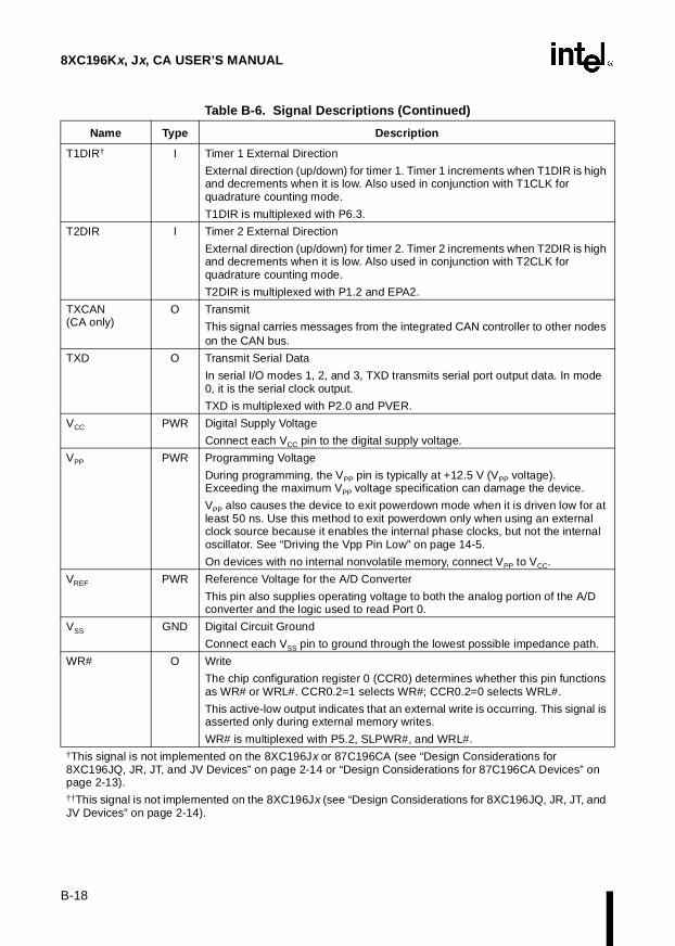
8XC196Kx, Jx, CA USER’S MANUAL
B-18
T1DIR† I Timer 1 External Direction
External direction (up/down) for timer 1. Timer 1 increments when T1DIR is high and decrements when it is low. Also used in conjunction with T1CLK for quadrature counting mode.
T1DIR is multiplexed with P6.3.
T2DIR I Timer 2 External Direction
External direction (up/down) for timer 2. Timer 2 increments when T2DIR is high and decrements when it is low. Also used in conjunction with T2CLK for quadrature counting mode.
T2DIR is multiplexed with P1.2 and EPA2.
TXCAN(CA only)
O Transmit
This signal carries messages from the integrated CAN controller to other nodes on the CAN bus.
TXD O Transmit Serial Data
In serial I/O modes 1, 2, and 3, TXD transmits serial port output data. In mode 0, it is the serial clock output.
TXD is multiplexed with P2.0 and PVER.
VCC PWR Digital Supply Voltage
Connect each VCC pin to the digital supply voltage.
VPP PWR Programming Voltage
During programming, the VPP pin is typically at +12.5 V (VPP voltage). Exceeding the maximum VPP voltage specification can damage the device.
VPP also causes the device to exit powerdown mode when it is driven low for at least 50 ns. Use this method to exit powerdown only when using an external clock source because it enables the internal phase clocks, but not the internal oscillator. See “Driving the Vpp Pin Low” on page 14-5.
On devices with no internal nonvolatile memory, connect VPP to VCC.
VREF PWR Reference Voltage for the A/D Converter
This pin also supplies operating voltage to both the analog portion of the A/D converter and the logic used to read Port 0.
VSS GND Digital Circuit Ground
Connect each VSS pin to ground through the lowest possible impedance path.
WR# O Write
The chip configuration register 0 (CCR0) determines whether this pin functions as WR# or WRL#. CCR0.2=1 selects WR#; CCR0.2=0 selects WRL#.
This active-low output indicates that an external write is occurring. This signal is asserted only during external memory writes.
WR# is multiplexed with P5.2, SLPWR#, and WRL#.
Table B-6. Signal Descriptions (Continued)
Name Type Description
†This signal is not implemented on the 8XC196Jx or 87C196CA (see “Design Considerations for 8XC196JQ, JR, JT, and JV Devices” on page 2-14 or “Design Considerations for 87C196CA Devices” on page 2-13).††This signal is not implemented on the 8XC196Jx (see “Design Considerations for 8XC196JQ, JR, JT, and JV Devices” on page 2-14).

B-19
SIGNAL DESCRIPTIONS
B.4 DEFAULT CONDITIONS
Table B-8 lists the default functions of the I/O and control pins of the 8XC196Kx with their valuesduring various operating conditions. Tables B-9 and B-10 list the same information for the8XC196Jx and 87C196CA, respectively. Table B-7 defines the symbols used to represent the pinstatus. Refer to the DC Characteristics table in the datasheet for actual specifications for VOL, VIL,VOH, and VIH.
WRH#† O Write High
The chip configuration register 0 (CCR0) determines whether this pin functions as BHE# or WRH#. CCR0.2=1 selects BHE#; CCR0.2=0 selects WRH#.
During 16-bit bus cycles, this active-low output signal is asserted for high-byte writes and word writes to external memory. During 8-bit bus cycles, WRH# is asserted for all write operations.
WRH# is multiplexed with P5.5 and BHE#.
WRL# O Write Low
The chip configuration register 0 (CCR0) determines whether this pin functions as WR# or WRL#. CCR0.2=1 selects WR#; CCR0.2=0 selects WRL#.
During 16-bit bus cycles, this active-low output signal is asserted for low-byte writes and word writes. During 8-bit bus cycles, WRL# is asserted for all write operations.
WRL# is multiplexed with P5.2, SLPWR#, and WR#.
XTAL1 I Input Crystal/Resonator or External Clock Input
Input to the on-chip oscillator and the internal clock generators. The internal clock generators provide the peripheral clocks, CPU clock, and CLKOUT signal. When using an external clock source instead of the on-chip oscillator, connect the clock input to XTAL1. The external clock signal must meet the VIH specification for XTAL1 (see datasheet).
XTAL2 O Inverted Output for the Crystal/Resonator
Output of the on-chip oscillator inverter. Leave XTAL2 floating when the design uses a external clock source instead of the on-chip oscillator.
Table B-7. Definition of Status Symbols
Symbol Definition Symbol Definition
0 Voltage less than or equal to VOL, VIL MD0 Medium pull-down
1 Voltage greater than or equal to VOH, VIH MD1 Medium pull-up
HiZ High impedance WK0 Weak pull-down
LoZ0 Low impedance; strongly driven low WK1 Weak pull-up
LoZ1 Low impedance; strongly driven high ODIO Open-drain I/O
Table B-6. Signal Descriptions (Continued)
Name Type Description
†This signal is not implemented on the 8XC196Jx or 87C196CA (see “Design Considerations for 8XC196JQ, JR, JT, and JV Devices” on page 2-14 or “Design Considerations for 87C196CA Devices” on page 2-13).††This signal is not implemented on the 8XC196Jx (see “Design Considerations for 8XC196JQ, JR, JT, and JV Devices” on page 2-14).

8XC196Kx, Jx, CA USER’S MANUAL
B-20
Table B-8. 8XC196K x Pin Status
Pins MultiplexedWith
During RESET#Active
Upon RESET#Inactive (Note 9)
Idle Power-down
P0.7:0 ACH7:0 HiZ HiZ HiZ HiZ
P1.0 EPA0/T2CLK WK1 WK1 (Note 3) (Note 3)
P1.1 EPA1 WK1 WK1 (Note 3) (Note 3)
P1.2 EPA2/T2DIR WK1 WK1 (Note 3) (Note 3)
P1.7:3 EPA7:3 WK1 WK1 (Note 3) (Note 3)
P2.0 TXD WK1 WK1 (Note 3) (Note 3)
P2.1 RXD WK1 WK1 (Note 3) (Note 3)
P2.2 EXTINT WK1 WK1 (Note 3) (Note 3)
P2.3 BREQ# WK1 WK1 (Note 3) (Note 3)
P2.4 INTOUT# WK1 WK1 (Note 3) (Note 3)
P2.5 HOLD# WK1 WK1 (Note 3) (Note 3)
P2.6 HLDA#
& ONCE# (KT, KS)MD1 MD1 (Note 3) (Note 3)
P2.7 CLKOUT CLKOUT active, LoZ0/1 (Note 7)
CLKOUT active, LoZ0/1
(Note 3) (Note 4)
P3.7:0 AD7:0 WK1 HiZ (Note 6) (Note 6)
P4.7:0 AD15:8 WK1 HiZ (Note 6) (Note 6)
P5.0 ALE/ADV#/SLPALE WK1 WK1 (Note 1) (Note 1)
P5.1 INST/SLPCS# WK0 WK0 (Note 1) (Note 1)
P5.2 WR#/WRL#/SLPWR# WK1 WK1 (Note 3) (Note 3)
P5.3 RD#/SLPRD# WK1 WK1 (Note 3) (Note 3)
P5.4 SLPINT
& ONCE# (KR, KQ)MD1 MD1 (Note 3) (Note 3)
P5.5 BHE#/WRH# WK1 WK1 (Note 1) (Note 1)
P5.6 READY WK1 WK1 (Note 2) (Note 2)
P5.7 BUSWIDTH WK1 WK1 (Note 2) (Note 2)
P6.0 EPA8/COMP0 WK1 WK1 (Note 3) (Note 3)
P6.1 EPA9/COMP1 WK1 WK1 (Note 3) (Note 3)
P6.2 T1CLK WK1 WK1 (Note 3) (Note 3)
P6.3 T1DIR WK1 WK1 (Note 3) (Note 3)
P6.4 SC0 WK1 WK1 (Note 3) (Note 3)
P6.5 SD0 WK1 WK1 (Note 3) (Note 3)
P6.6 SC1 WK1 WK1 (Note 3) (Note 3)
P6.7 SD1 WK1 WK1 (Note 3) (Note 3)
EA# — WK1 (Note 8) WK1 WK1 WK1
NMI — WK0 (Note 8) WK0 WK0 WK0
RESET# — LoZ0 MD1 MD1 MD1
VPP — HiZ HiZ LoZ1 LoZ1

B-21
SIGNAL DESCRIPTIONS
XTAL1 — Osc input, HiZ Osc input, HiZ Osc input,HiZ
Osc input, HiZ
XTAL2 — Osc output, LoZ0/1
Osc output, LoZ0/1
Osc output, LoZ0/1 (Note 5)
NOTES:1. If P5_MODE.x = 0, port is as programmed.
If P5_MODE.x = 1 and HLDA# = 1, P5.0 and P5.1 are LoZ0; P5.5 is LoZ1.If P5_MODE.x = 1 and HLDA# = 0, port is HiZ.
2. If P5_MODE.x = 0, port is as programmed. If P5_MODE.x = 1, port is HiZ.3. If Px_MODE.x = 0, port is as programmed.
If Px_MODE.x = 1, pin is as specified by Px_DIR and the associated peripheral.4. If P2_MODE.7 = 0, pin is as programmed. If P2_MODE.7 = 1, pin is LoZ0.5. If XTAL1 = 0, pin is LoZ1. If XTAL1 = 1, pin is LoZ0.6. If EA# = 0, port is HiZ. If EA# = 1, port is open-drain I/O.7. On the 8XC196KS and KT, CLKOUT is HiZ during RESET# active.8. Although these signals are weakly pulled high or low, do not allow them to float. Always tie these sig-
nals to their inactive state (VCC or VSS) if they are not connected to an external device.9. The values in this column are valid until user code configures the specific signal (i.e., until Px_MODE
is written).
Table B-9. 8XC196J x Pin Status
Pins MultiplexedWith
During RESET#Active
Upon RESET#Inactive(Note 8)
Idle Power-down
P0.7:2 ACH7:2 HiZ HiZ HiZ HiZ
P1.0 EPA0/T2CLK WK1 WK1 (Note 3) (Note 3)
P1.1 EPA1 WK1 WK1 (Note 3) (Note 3)
P1.2 EPA2/T2DIR WK1 WK1 (Note 3) (Note 3)
P1.3 EPA3 WK1 WK1 (Note 3) (Note 3)
P2.0 TXD WK1 WK1 (Note 3) (Note 3)
P2.1 RXD WK1 WK1 (Note 3) (Note 3)
P2.2 EXTINT WK1 WK1 (Note 3) (Note 3)
P2.4 — WK1 WK1 (Note 3) (Note 3)
P2.6 ONCE# MD1 MD1 (Note 3) (Note 3)
P2.7 CLKOUT CLKOUT active, LoZ0/1 (Note 9)
CLKOUT active, LoZ0/1
(Note 3) (Note 4)
P3.7:0 AD7:0 WK1 HiZ (Note 6) (Note 6)
P4.7:0 AD15:8 WK1 HiZ (Note 6) (Note 6)
P5.0 ALE/ADV# WK1 WK1 (Note 1) (Note 1)
P5.2 WR#/WRL# WK1 WK1 (Note 3) (Note 3)
P5.3 RD# WK1 WK1 (Note 3) (Note 3)
P6.0 EPA8/COMP0 WK1 WK1 (Note 3) (Note 3)
P6.1 EPA9/COMP1 WK1 WK1 (Note 3) (Note 3)
Table B-8. 8XC196K x Pin Status (Continued)
Pins MultiplexedWith
During RESET#Active
Upon RESET#Inactive (Note 9)
Idle Power-down

8XC196Kx, Jx, CA USER’S MANUAL
B-22
P6.4 SC0 WK1 WK1 (Note 3) (Note 3)
P6.5 SD0 WK1 WK1 (Note 3) (Note 3)
P6.6 SC1 WK1 WK1 (Note 3) (Note 3)
P6.7 SD1 WK1 WK1 (Note 3) (Note 3)
EA# — WK1 (Note 7) WK1 WK1 WK1
RESET# — LoZ0 MD1 MD1 MD1
VPP — HiZ HiZ LoZ1 LoZ1
XTAL1 — Osc input, HiZ Osc input, HiZ Osc input, HiZ
Osc input, HiZ
XTAL2 — Osc output, LoZ0/1
Osc output, LoZ0/1
Osc output, LoZ0/1
(Note 5)
NOTES:1. If P5_MODE.x = 0, port is as programmed.
If P5_MODE.x = 1 and HLDA# = 1, P5.0 and P5.1 are LoZ0; P5.5 is LoZ1.If P5_MODE.x = 1 and HLDA# = 0, port is HiZ.
2. If P5_MODE.x = 0, port is as programmed. If P5_MODE.x = 1, port is HiZ.3. If Px_MODE.x = 0, port is as programmed.
If Px_MODE.x = 1, pin is as specified by Px_DIR and the associated peripheral.4. If P2_MODE.7 = 0, pin is as programmed. If P2_MODE.7 = 1, pin is LoZ0.5. If XTAL1 = 0, pin is LoZ1. If XTAL1 = 1, pin is LoZ0.6. If EA# = 0, port is HiZ. If EA# = 1, port is open-drain I/O.7. Although EA# is weakly pulled high, do not allow it to float. Always tie EA# to VCC if it is not connected
to an external device.8. The values in this column are valid until user code configures the specific signal (i.e., until Px_MODE
is written).9. On the 8XC196JT, CLKOUT is HiZ during RESET# active.
Table B-10. 87C196CA Pin Status
Pins MultiplexedWith
During RESET#Active
Upon RESET#Inactive (Note 9) Idle Power-down
P0.7:2 ACH7:2 HiZ HiZ HiZ HiZ
P1.0 EPA0/T2CLK WK1 WK1 (Note 3) (Note 3)
P1.1 EPA1 WK1 WK1 (Note 3) (Note 3)
P1.2 EPA2/T2DIR WK1 WK1 (Note 3) (Note 3)
P1.3 EPA3 WK1 WK1 (Note 3) (Note 3)
P2.0 TXD WK1 WK1 (Note 3) (Note 3)
P2.1 RXD WK1 WK1 (Note 3) (Note 3)
P2.2 EXTINT WK1 WK1 (Note 3) (Note 3)
P2.4 — WK1 WK1 (Note 3) (Note 3)
P2.6 ONCE# MD1 MD1 (Note 3) (Note 3)
P2.7 CLKOUT CLKOUT active, LoZ0/1
CLKOUT active, LoZ0/1
(Note 3) (Note 4)
P3.7:0 AD7:0 WK1 HiZ (Note 6) (Note 6)
Table B-9. 8XC196J x Pin Status (Continued)
Pins MultiplexedWith
During RESET#Active
Upon RESET#Inactive(Note 8)
Idle Power-down
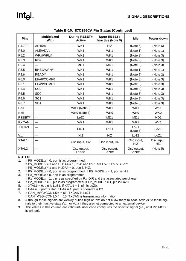
B-23
SIGNAL DESCRIPTIONS
P4.7:0 AD15:8 WK1 HiZ (Note 6) (Note 6)
P5.0 ALE/ADV# WK1 WK1 (Note 1) (Note 1)
P5.2 WR#/WRL# WK1 WK1 (Note 3) (Note 3)
P5.3 RD# WK1 WK1 (Note 3) (Note 3)
P5.4 — MD1 MD1 (Note 3) (Note 3)
P5.5 BHE#/WRH# WK1 WK1 (Note 1) (Note 1)
P5.6 READY WK1 WK1 (Note 2) (Note 2)
P6.0 EPA8/COMP0 WK1 WK1 (Note 3) (Note 3)
P6.1 EPA9/COMP1 WK1 WK1 (Note 3) (Note 3)
P6.4 SC0 WK1 WK1 (Note 3) (Note 3)
P6.5 SD0 WK1 WK1 (Note 3) (Note 3)
P6.6 SC1 WK1 WK1 (Note 3) (Note 3)
P6.7 SD1 WK1 WK1 (Note 3) (Note 3)
EA# — WK1 (Note 8) WK1 WK1 WK1
NMI — WK0 (Note 8) WK0 WK0 WK0
RESET# — LoZ0 MD1 MD1 MD1
RXCAN — WK1 WK1 WK1 WK1
TXCAN — LoZ1 LoZ1 LoZ1(Note 7) LoZ1
VPP — HiZ HiZ LoZ1 LoZ1
XTAL1 — Osc input, HiZ Osc input, HiZ Osc input, HiZ
Osc input, HiZ
XTAL2 — Osc output, LoZ0/1
Osc output, LoZ0/1
Osc output, LoZ0/1
(Note 5)
NOTES:1. If P5_MODE.x = 0, port is as programmed.
If P5_MODE.x = 1 and HLDA# = 1, P5.0 and P5.1 are LoZ0; P5.5 is LoZ1.If P5_MODE.x = 1 and HLDA# = 0, port is HiZ.
2. If P5_MODE.x = 0, port is as programmed. If P5_MODE.x = 1, port is HiZ.3. If Px_MODE.x = 0, port is as programmed.
If Px_MODE.x = 1, pin is as specified by Px_DIR and the associated peripheral.4. If P2_MODE.7 = 0, pin is as programmed. If P2_MODE.7 = 1, pin is LoZ0.5. If XTAL1 = 0, pin is LoZ1. If XTAL1 = 1, pin is LoZ0.6. If EA# = 0, port is HiZ. If EA# = 1, port is open-drain I/O.7. If CAN_MSGxCON1.5:4 = 01, TXCAN is LoZ1.
If CAN_MSGxCON1.5:4 = 10, TXCAN is transmitting information. 8. Although these signals are weakly pulled high or low, do not allow them to float. Always tie these sig-
nals to their inactive state (VCC or VSS) if they are not connected to an external device.9. The values in this column are valid until user code configures the specific signal (i.e., until Px_MODE
is written).
Table B-10. 87C196CA Pin Status (Continued)
Pins MultiplexedWith
During RESET#Active
Upon RESET#Inactive (Note 9) Idle Power-down

CRegisters

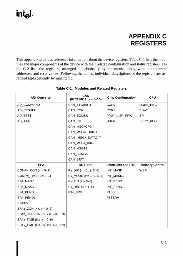
C-1
APPENDIX CREGISTERS
This appendix provides reference information about the device registers. Table C-1 lists the mod-ules and major components of the device with their related configuration and status registers. Ta-ble C-2 lists the registers, arranged alphabetically by mnemonic, along with their names,addresses, and reset values. Following the tables, individual descriptions of the registers are ar-ranged alphabetically by mnemonic.
Table C-1. Modules and Related Registers
A/D Converter CAN(87C196CA, x = 0–15) Chip Configuration CPU
AD_COMMAND CAN_BTIME0–1 CCR0 ONES_REG
AD_RESULT CAN_CON CCR1 PSW
AD_TEST CAN_EGMSK PPW (or SP_PPW) SP
AD_TIME CAN_INT USFR ZERO_REG
CAN_MSGxCFG
CAN_MSGxCON0–1
CAN_ MSGx_DATA0–7
CAN_MSGx_ID0–3
CAN_MSG15
CAN_SGMSK
CAN_STAT
EPA I/O Ports Interrupts and PTS Memory Control
COMPx_CON (x = 0–1) Px_DIR (x = 1, 2, 5, 6) INT_MASK WSR
COMPx_TIME (x = 0–1) Px_MODE (x = 1, 2, 5, 6) INT_MASK1
EPA_MASK Px_PIN (x = 0–6) INT_PEND
EPA_MASK1 Px_REG (x = 1–6) INT_PEND1
EPA_PEND P34_DRV PTSSEL
EPA_PEND1 PTSSRV
EPAIPV
EPAx_CON (Kx, x = 0–9)
EPAx_CON (CA, Jx, x = 0–3, 8, 9)
EPAx_TIME (Kx, x = 0–9)
EPAx_TIME (CA, Jx, x = 0–3, 8, 9)

8XC196Kx, Jx, CA USER’S MANUAL
C-2
Serial Port Slave Port(8XC196Kx)
Synch. Serial Port(x = 0–1)
Timers(x = 1–2)
SBUF_RX SLP_CMD SSIO_BAUD TIMERx
SBUF_TX SLP_CON SSIOx_BUF TxCONTROL
SP_BAUD SLP_STAT SSIOx_CON WATCHDOG
SP_CON
SP_STATUS
Table C-2. Register Name, Address, and Reset Status
Register Mnemonic Register Name Hex
Address
Binary Reset Value
High Low
AD_COMMAND A/D Command 1FACH 1100 0000
AD_RESULT A/D Result 1FAAH 0111 1111 1000 0000
AD_TEST A/D Test 1FAEH 1100 0000
AD_TIME A/D Time 1FAFH 1111 1111
CAN_BTIME0 (CA) CAN Bit Timing 0 1E3FH Unchanged††
CAN_BTIME1 (CA) CAN Bit Timing 1 1E4FH Unchanged††
CAN_CON (CA) CAN Control 1E00H 0000 0001
CAN_EGMSK (CA) CAN Extended Global Mask 1E08H1E09H1E0AH1E0BH
Unchanged††
CAN_INT (CA) CAN Interrupt Pending 1E5FH 0000 0000
CAN_MSGxCFG (CA)† CAN Message Object x Config 1Ey6H Unchanged††
CAN_MSGxCON0 (CA)† CAN Message Object x Control 0 1Ey0H Unchanged††
CAN_MSGxCON1 (CA)† CAN Message Object x Control 1 1Ey1H Unchanged††
CAN_MSGxDATA0 (CA)† CAN Message Object Data 0 1Ey7H Unchanged††
CAN_MSGxDATA1 (CA)† CAN Message Object Data 1 1Ey8H Unchanged††
CAN_MSGxDATA2 (CA)† CAN Message Object Data 2 1Ey9H Unchanged††
CAN_MSGxDATA3 (CA)† CAN Message Object Data 3 1EyAH Unchanged††
CAN_MSGxDATA4 (CA)† CAN Message Object Data 4 1EyBH Unchanged††
CAN_MSGxDATA5 (CA)† CAN Message Object Data 5 1EyCH Unchanged††
CAN_MSGxDATA6 (CA)† CAN Message Object Data 6 1EyDH Unchanged††
CAN_MSGxDATA7 (CA)† CAN Message Object Data 7 1EyEH Unchanged††
CAN_MSGxID0 (CA)† CAN Message Object Ident 0 1Ey2H Unchanged††
† x = 1–15; y = 1–F†† After reset, this register contains the value that was written to it before reset.
Table C-1. Modules and Related Registers (Continued)

C-3
REGISTERS
CAN_MSGxID1 (CA)† CAN Message Object Ident 1 1Ey3H Unchanged††
CAN_MSGxID2 (CA)† CAN Message Object Ident 2 1Ey4H Unchanged††
CAN_MSGxID3 (CA)† CAN Message Object Ident 3 1Ey5H Unchanged††
CAN_MSK15 (CA) CAN Message 15 Mask 1E0CH1E0DH1E0EH1E0FH
Unchanged††
CAN_SGMSK (CA) CAN Standard Global Mask 1E06H Unchanged††
CAN_STAT (CA) CAN Status 1E01H XXXX XXXX
CCR0 Chip Configuration 0 2018H XXXX XXXX
CCR1 Chip Configuration 1 201AH XXXX XXXX
COMP0_CON EPA Compare 0 Control 1F88H 0000 0000
COMP0_TIME EPA Compare 0 Time 1F8AH XXXX XXXX XXXX XXXX
COMP1_CON EPA Compare 1 Control 1F8CH 0000 0000
COMP1_TIME EPA Compare 1 Time 1F8EH XXXX XXXX XXXX XXXX
EPA_MASK EPA Mask 1FA0H 0000 0000 0000 0000
EPA_MASK1 EPA Mask 1 1FA4H 0000 0000
EPA_PEND EPA Pending 1FA2H 0000 0000 0000 0000
EPA_PEND1 EPA Pending 1 1FA6H 0000 0000
EPA0_CON EPA Capture/Comp 0 Control 1F60H 0000 0000
EPA0_TIME EPA Capture/Comp 0 Time 1F62H XXXX XXXX XXXX XXXX
EPA1_CON EPA Capture/Comp 1 Control 1F64H 1111 1110 0000 0000
EPA1_TIME EPA Capture/Comp 1 Time 1F66H XXXX XXXX XXXX XXXX
EPA2_CON EPA Capture/Comp 2 Control 1F68H 0000 0000
EPA2_TIME EPA Capture/Comp 2 Time 1F6AH XXXX XXXX XXXX XXXX
EPA3_CON EPA Capture/Comp 3 Control 1F6CH 1111 1110 0000 0000
EPA3_TIME EPA Capture/Comp 3 Time 1F6EH XXXX XXXX XXXX XXXX
EPA4_CON (Kx) EPA Capture/Comp 4 Control 1F70H 0000 0000
EPA4_TIME (Kx) EPA Capture/Comp 4 Time 1F72H XXXX XXXX XXXX XXXX
EPA5_CON (Kx) EPA Capture/Comp 5 Control 1F74H 0000 0000
EPA5_TIME (Kx) EPA Capture/Comp 5 Time 1F76H XXXX XXXX XXXX XXXX
EPA6_CON (Kx) EPA Capture/Comp 6 Control 1F78H 0000 0000
EPA6_TIME (Kx) EPA Capture/Comp 6 Time 1F7AH XXXX XXXX XXXX XXXX
Table C-2. Register Name, Address, and Reset Status (Continued)
Register Mnemonic Register Name Hex
Address
Binary Reset Value
High Low
† x = 1–15; y = 1–F†† After reset, this register contains the value that was written to it before reset.

8XC196Kx, Jx, CA USER’S MANUAL
C-4
EPA7_CON (Kx) EPA Capture/Comp 7 Control 1F7CH 0000 0000
EPA7_TIME (Kx) EPA Capture/Comp 7 Time 1F7EH XXXX XXXX XXXX XXXX
EPA8_CON EPA Capture/Comp 8 Control 1F80H 0000 0000
EPA8_TIME EPA Capture/Comp 8 Time 1F82H XXXX XXXX XXXX XXXX
EPA9_CON EPA Capture/Comp 9 Control 1F84H 0000 0000
EPA9_TIME EPA Capture/Comp 9 Time 1F86H XXXX XXXX XXXX XXXX
EPAIPV EPA Interrupt Priority Vector 1FA8H 0000 0000
INT_MASK Interrupt Mask 0008H 0000 0000
INT_MASK1 Interrupt Mask 1 0013H 0000 0000
INT_PEND Interrupt Pending 0009H 0000 0000
INT_PEND1 Interrupt Pending 1 0012H 0000 0000
ONES_REG Ones Register 0002H 1111 1111 1111 1111
P0_PIN Port 0 Pin Input 1FDAH XXXX XXXX
P1_DIR Port 1 I/O Direction 1FD2H 1111 1111
P1_MODE Port 1 Mode 1FD0H 0000 0000
P1_PIN Port 1 Pin Input 1FD6H XXXX XXXX
P1_REG Port 1 Data Output 1FD4H 1111 1111
P2_DIR Port 2 I/O Direction 1FCBH 0111 1111
P2_MODE Port 2 Mode 1FC9H 1000 0000
P2_PIN Port 2 Pin Input 1FCFH 1XXX XXXX
P2_REG Port 2 Data Output 1FCDH 0111 1111
P3_PIN Port 3 Pin Input 1FFEH XXXX XXXX
P3_REG Port 3 Data Output 1FFCH 1111 1111
P34_DRV Port 3/4 Push-pull Enable 1FF4H 0000 0000
P4_PIN Port 4 Pin Input 1FFFH XXXX XXXX
P4_REG Port 4 Data Output 1FFDH 1111 1111
P5_DIR Port 5 I/O Direction 1FF3H 1111 1111
P5_MODE Port 5 Mode 1FF1H 1000 0000
P5_PIN Port 5 Pin Input 1FF7H 1XXX XXXX
P5_REG Port 5 Data Output 1FF5H 1111 1111
P6_DIR Port 6 I/O Direction 1FD3H 1111 1111
P6_MODE Port 6 Mode 1FD1H 0000 0000
Table C-2. Register Name, Address, and Reset Status (Continued)
Register Mnemonic Register Name Hex
Address
Binary Reset Value
High Low
† x = 1–15; y = 1–F†† After reset, this register contains the value that was written to it before reset.

C-5
REGISTERS
P6_PIN Port 6 Pin Input 1FD7H XXXX XXXX
P6_REG Port 6 Data Output 1FD5H 1111 1111
PPW (or SP_PPW) Programming Pulse Width
PSW Program Status Word
PTSSEL PTS Select 0004H 0000 0000 0000 0000
PTSSRV PTS Service 0006H 0000 0000 0000 0000
SBUF_RX Serial Port Receive Buffer 1FB8H 0000 0000
SBUF_TX Serial Port Transmit Buffer 1FBAH 0000 0000
SLP_CMD (Kx) Slave Port Command 1FFAH 0000 0000
SLP_CON (Kx) Slave Port Control 1FFBH 0000 0000
SLP_STAT (Kx) Slave Port Status 1FF8H 0000 0000
SP Stack Pointer 0018H XXXX XXXX XXXX XXXX
SP_BAUD Serial Port Baud Rate 1FBCH 0000 0000 0000 0000
SP_CON Serial Port Control 1FBBH 0000 0000
SP_STATUS Serial Port Status 1FB9H 0000 1011
SSIO_BAUD Syn Serial Port Baud Rate 1FB4H 0XXX XXXX
SSIO0_BUF Syn Serial Port 0 Buffer 1FB0H 0000 0000
SSIO0_CON Syn Serial Port 0 Control 1FB1H 0000 0000
SSIO1_BUF Syn Serial Port 1 Buffer 1FB2H 0000 0000
SSIO1_CON Syn Serial Port 1 Control 1FB3H 0000 0000
T1CONTROL Timer 1 Control 1F98H 0000 0000
T2CONTROL Timer 2 Control 1F9CH 0000 0000
TIMER1 Timer 1 Value 1F9AH 0000 0000 0000 0000
TIMER2 Timer 2 Value 1F9EH 0000 0000 0000 0000
USFR UPROM Special Function Reg 1FF6H XXXX XXXX
WATCHDOG Watchdog Timer 000AH 0000 0000
WSR Window Selection 0014H 0000 0000
ZERO_REG Zero Register 0000H 0000 0000 0000 0000
Table C-2. Register Name, Address, and Reset Status (Continued)
Register Mnemonic Register Name Hex
Address
Binary Reset Value
High Low
† x = 1–15; y = 1–F†† After reset, this register contains the value that was written to it before reset.

8XC196Kx, Jx, CA USER’S MANUAL
C-6
AD_COMMAND
AD_COMMAND Address:Reset State:
1FACHC0H
The A/D command (AD_COMMAND) register selects the A/D channel number to be converted, controls whether the A/D converter starts immediately or with an EPA command, and selects the conversion mode.
7 0
— — M1 M0 GO ACH2 ACH1 ACH0
Bit Number
Bit Mnemonic Function
7:6 — Reserved; for compatibility with future devices, write zeros to these bits.
5:4 M1:0 A/D Mode (Note 1)
These bits determine the A/D mode.
M1 M0 Mode
0 0 10-bit conversion0 1 8-bit conversion1 0 threshold detect high1 1 threshold detect low
3 GO A/D Conversion Trigger (Note 2)
Writing this bit arms the A/D converter. The value that you write to it determines at what point a conversion is to start.
1 = start immediately0 = EPA initiates conversion
2:0 ACH2:0 A/D Channel Selection
Write the A/D conversion channel number to these bits. The 87C196CA, 8XC196Jx devices have six A/D channels, numbered 2–7. The 8XC196Kx devices have eight channels, numbered 0–7.
NOTES:1. While a threshold-detection mode is selected for an analog input pin, no other conversion can be
started. If another value is loaded into AD_COMMAND, the threshold-detection mode is disabledand the new command is executed.
2. It is the act of writing to the GO bit, rather than its value, that starts a conversion. Even if the GObit has the desired value, you must set it again to start a conversion immediately or clear it againto arm it for an EPA-initiated conversion.

C-7
REGISTERS
AD_RESULT (Read)
AD_RESULT (Read) Address:Reset State:
1FAAH7F80H
The A/D result (AD_RESULT) register consists of two bytes. The high byte contains the eight most-significant bits from the A/D converter. The low byte contains the two least-significant bits from a ten-bit A/D conversion, indicates the A/D channel number that was used for the conversion, and indicates whether a conversion is currently in progress.
15 8
ADRLT9 ADRLT8 ADRLT7 ADRLT6 ADRLT5 ADRLT4 ADRLT3 ADRLT2
7 0
ADRLT1 ADRLT0 — — STATUS ACH2 ACH1 ACH0
Bit Number
Bit Mnemonic Function
15:6 ADRLT9:0 A/D Result
These bits contain the A/D conversion result.
5:4 — Reserved. These bits are undefined.
3 STATUS A/D Status
Indicates the status of the A/D converter. Up to 8 state times are required to set this bit following a start command. When testing this bit, wait at least the 8 state times.
1 = A/D conversion is in progress0 = A/D is idle
2:0 ACH2:0 A/D Channel Number
These bits indicate the A/D channel number that was used for the conversion. The 87C196CA, 8XC196Jx devices have six channel inputs. These channels are numbered 2–7. The 8XC196Kx devices have eight channels, numbered 0–7.

8XC196Kx, Jx, CA USER’S MANUAL
C-8
AD_RESULT (Write)
AD_RESULT (Write) Address:Reset State:
1FAAH7F80H
The high byte of the A/D result (AD_RESULT) register can be written to set the reference voltage for the A/D threshold-detection modes.
15 8
REFV7 REFV6 REFV5 REFV4 REFV3 REFV2 REFV1 REFV0
7 0
— — — — — — — —
Bit Number
Bit Mnemonic Function
15:8 REFV7:0 Reference Voltage
These bits specify the threshold value. This selects a reference voltage which is compared with an analog input pin. When the voltage on the analog input pin crosses over (detect high) or under (detect low) the threshold value, the A/D conversion complete interrupt flag is set.
Use the following formula to determine the value to write this register for a given threshold voltage.
7:0 — Reserved; for compatibility with future devices, write zeros to these bits.
reference voltagedesired threshold voltage 256×
VREF ANGND–-----------------------------------------------------------------------------------=
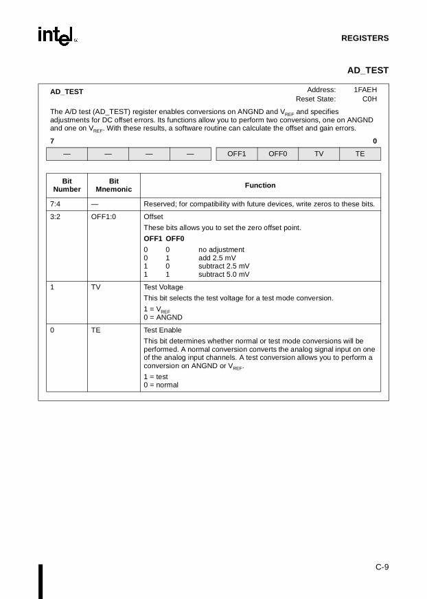
C-9
REGISTERS
AD_TEST
AD_TEST Address:Reset State:
1FAEHC0H
The A/D test (AD_TEST) register enables conversions on ANGND and VREF and specifies adjustments for DC offset errors. Its functions allow you to perform two conversions, one on ANGND and one on VREF. With these results, a software routine can calculate the offset and gain errors.
7 0
— — — — OFF1 OFF0 TV TE
Bit Number
Bit Mnemonic Function
7:4 — Reserved; for compatibility with future devices, write zeros to these bits.
3:2 OFF1:0 Offset
These bits allows you to set the zero offset point.
OFF1 OFF0
0 0 no adjustment0 1 add 2.5 mV1 0 subtract 2.5 mV1 1 subtract 5.0 mV
1 TV Test Voltage
This bit selects the test voltage for a test mode conversion.
1 = VREF0 = ANGND
0 TE Test Enable
This bit determines whether normal or test mode conversions will be performed. A normal conversion converts the analog signal input on one of the analog input channels. A test conversion allows you to perform a conversion on ANGND or VREF.
1 = test0 = normal

8XC196Kx, Jx, CA USER’S MANUAL
C-10
AD_TIME
AD_TIME Address:Reset State:
1FAFHFFH
The A/D time (AD_TIME) register programs the sample window time and the conversion time for each bit.
7 0
SAM2 SAM1 SAM0 CONV4 CONV3 CONV2 CONV1 CONV0
Bit Number
Bit Mnemonic Function
7:5 SAM2:0 A/D Sample Time
These bits specify the sample time. Use the following formula to compute the sample time.
where:
SAM = 1 to 7
TSAM = the sample time, in µsec, from the data sheet
FOSC = the XTAL1 frequency, in MHz
4:0 CONV4:0 A/D Convert Time
These bits specify the conversion time. Use the following formula to compute the conversion time.
where:
CONV= 2 to 31
TCONV = the conversion time, in µsec, from the data sheet
FOSC = the XTAL1 frequency, in MHz
B = the number of bits to be converted (8 or 10)
NOTES:1. The register programs the speed at which the A/D can run — not the speed at which it can con-
vert correctly. Consult the data sheet for recommended values.2. Initialize the AD_TIME register before initializing the AD_COMMAND register.3. Do not write to this register while a conversion is in progress; the results are unpredictable.
SAMTSAM FOSC× 2–
8--------------------------------------------=
CONVTCONV FOSC× 3–
2 B×----------------------------------------------- 1–=
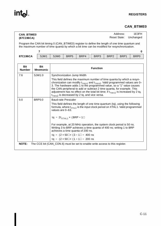
C-11
REGISTERS
CAN_BTIME0
CAN_BTIME0(87C196CA)
Address:Reset State:
1E3FHUnchanged
Program the CAN bit timing 0 (CAN_BTIME0) register to define the length of one time quantum and the maximum number of time quanta by which a bit time can be modified for resynchronization.
7 0
87C196CA SJW1 SJW0 BRP5 BRP4 BRP3 BRP2 BRP1 BRP0
BitNumber
BitMnemonic Function
7:6 SJW1:0 Synchronization Jump Width
This field defines the maximum number of time quanta by which a resyn-chronization can modify tTSEG1 and tTSEG2. Valid programmed values are 0–3. The hardware adds 1 to the programmed value, so a “1” value causes the CAN peripheral to add or subtract 2 time quanta, for example. This adjustment has no effect on the total bit time; if tTSEG1 is increased by 2 tq, tTSEG2 is decreased by 2 tq, and vice versa.
5:0 BRP5:0 Baud-rate Prescaler
This field defines the length of one time quantum (tq), using the following formula, where tXTAL1 is the input clock period on XTAL1. Valid programmed values are 0–63.
For example, at 20 MHz operation, the system clock period is 50 ns. Writing 3 to BRP achieves a time quanta of 400 ns; writing 1 to BRP achieves a time quanta of 200 ns.
NOTE: The CCE bit (CAN_CON.6) must be set to enable write access to this register.
tq 2tXTAL1 BRP 1+( )×=
tq 2 50×( ) 3 1+( )× 400 ns= =
tq 2 50×( ) 1 1+( )× 200 ns= =

8XC196Kx, Jx, CA USER’S MANUAL
C-12
CAN_BTIME1
CAN_BTIME1(87C196CA)
Address:Reset State:
1E4FHUnchanged
Program the CAN bit timing 1 (CAN_BTIME1) register to define the sample time and the sample mode. The CAN controller samples the bus during the last one (in single-sample mode) or three (in three-sample mode) time quanta of tTSEG1, and initiates a transmission at the end of tTSEG2. Therefore, specifying the lengths of tTSEG1 and tTSEG2 defines both the sample point and the trans-mission point.
7 0
87C196CA SPL TSEG2.2 TSEG2.1 TSEG2.0 TSEG1.3 TSEG1.2 TSEG1.1 TSEG1.0
BitNumber
BitMnemonic Function
7 SPL Sampling Mode
This bit determines how many samples are taken to determine a valid bit value.
1 = 3 samples, using majority logic0 = 1 sample
6:4 TSEG2 Time Segment 2
This field determines the length of time that follows the sample point within a bit time. Valid programmed values are 1–7; the hardware adds 1 to this value. (Note 2)
3:0 TSEG1 Time Segment 1
This field defines the length of time that precedes the sample point within a bit time. Valid programmed values are 2–15; the hardware adds 1 to this value. In three-sample mode, the hardware adds 2 time quanta to allow time for the two additional samples. (Note 2)
NOTES:1. The CCE bit (CAN_CON.6) must be set to enable write access to this register.2. For correct operation according to the CAN protocol, the total bit time length must be at least 8
time quanta, so the sum of the programmed values of TSEG1 and TSEG2 must be at least 5.(The total bit time is the sum of tSYNC_SEG + tTSEG1 + tTSEG2. The length of tSYNC_SEG is 1 timequanta, and the hardware adds 1 to both TSEG1 and TSEG2. Therefore, if TSEG1 + TSEG2 =5, the total bit length will be equal to 8 (1+5+1+1)).
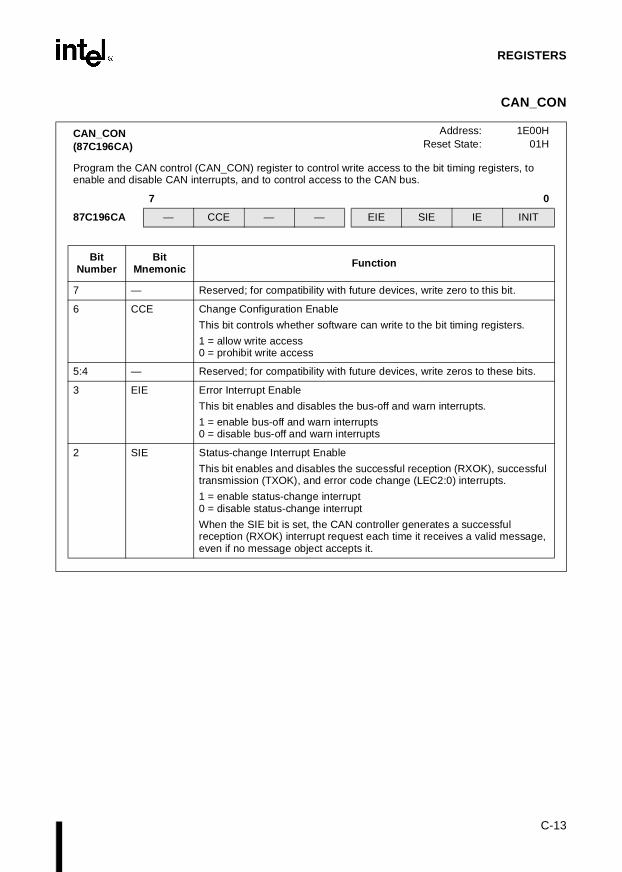
C-13
REGISTERS
CAN_CON
CAN_CON (87C196CA)
Address:Reset State:
1E00H01H
Program the CAN control (CAN_CON) register to control write access to the bit timing registers, to enable and disable CAN interrupts, and to control access to the CAN bus.
7 0
87C196CA — CCE — — EIE SIE IE INIT
BitNumber
BitMnemonic Function
7 — Reserved; for compatibility with future devices, write zero to this bit.
6 CCE Change Configuration Enable
This bit controls whether software can write to the bit timing registers.
1 = allow write access 0 = prohibit write access
5:4 — Reserved; for compatibility with future devices, write zeros to these bits.
3 EIE Error Interrupt Enable
This bit enables and disables the bus-off and warn interrupts.
1 = enable bus-off and warn interrupts 0 = disable bus-off and warn interrupts
2 SIE Status-change Interrupt Enable
This bit enables and disables the successful reception (RXOK), successful transmission (TXOK), and error code change (LEC2:0) interrupts.
1 = enable status-change interrupt 0 = disable status-change interrupt
When the SIE bit is set, the CAN controller generates a successful reception (RXOK) interrupt request each time it receives a valid message, even if no message object accepts it.

8XC196Kx, Jx, CA USER’S MANUAL
C-14
CAN_CON
1 IE Interrupt Enable
This bit globally enables and disables interrupts (error, status-change, and message object transmit and receive interrupts).
1 = enable interrupts 0 = disable interrupts
When the IE bit is set, an interrupt is generated only if the corresponding interrupt source’s enable bit (EIE or SIE in CAN_CON; TXIE or RXIE in CAN_MSGx_CON0) is also set. If the IE bit is clear, an interrupt request updates the CAN interrupt pending register, but does not generate an interrupt.
0 INIT Software Initialization Enable
Setting this bit isolates the CAN bus from the system. (If a transfer is in progress, it completes, but no additional transfers are allowed.)
1 = software initialization enabled0 = software initialization disabled
A hardware reset sets this bit, enabling you to configure the RAM without allowing any CAN bus activity. After a hardware reset or software initial-ization, clearing this bit completes the initialization. The CAN peripheral waits for a bus idle state (11 consecutive recessive bits) before partici-pating in bus activities.
Software can set this bit to stop all receptions and transmissions on the CAN bus. (To prevent transmission of a specific message object while its contents are being updated, set the CPUUPD bit in the individual message object’s control register 1. See “Configuring Message Objects” on page 12-20.)
Entering powerdown mode stops an in-progress CAN transmission immediately. To avoid stopping a CAN transmission while it is sending a dominant bit on the CAN bus, set the INIT bit before executing the IDLPD instruction.
The CAN peripheral also sets this bit to isolate the CAN bus when an error counter reaches 256. This isolation is called a bus-off condition. After a bus-off condition, clearing this bit initiates a bus-off recovery sequence, which clears the error counters. The CAN peripheral waits for 128 bus idle states (128 packets of 11 consecutive recessive bits), then resumes normal operation. (See “Bus-off State” on page 12-41.)
CAN_CON (Continued)(87C196CA)
Address:Reset State:
1E00H01H
Program the CAN control (CAN_CON) register to control write access to the bit timing registers, to enable and disable CAN interrupts, and to control access to the CAN bus.
7 0
87C196CA — CCE — — EIE SIE IE INIT
BitNumber
BitMnemonic Function

C-15
REGISTERS
CAN_EGMSK
CAN_EGMSK(87C196CA)
Address:Reset State:
Table C-3
Program the CAN extended global mask (CAN_EGMSK) register to mask (“don’t care”) specific message identifier bits for extended message objects.
31 24
87C196CA MSK4 MSK3 MSK2 MSK1 MSK0 — — —
23 16
MSK12 MSK11 MSK10 MSK9 MSK8 MSK7 MSK6 MSK5
15 8
MSK20 MSK19 MSK18 MSK17 MSK16 MSK15 MSK14 MSK13
7 0
MSK28 MSK27 MSK26 MSK25 MSK24 MSK23 MSK22 MSK21
BitNumber
BitMnemonic Function
31:27 MSK4:0 ID Mask
These bits individually mask incoming message identifier (ID) bits.
0 = mask the ID bit (accept either “0” or “1”)1 = accept only an exact match
26:24 — Reserved; for compatibility with future devices, write zeros to these bits.
23:1615:87:0
MSK12:5MSK20:13MSK28:21
ID Mask
These bits individually mask incoming message identifier (ID) bits.
0 = mask the ID bit (accept either “0” or “1”)1 = accept only an exact match
Table C-3. CAN_EGMSK Addresses and Reset Values
Register Address Reset Value
CAN_EGMSK (bits 0–7) 1E08H Unchanged††
CAN_EGMSK (bits 8–15) 1E09H Unchanged
CAN_EGMSK (bits 16–23) 1E0AH Unchanged
CAN_EGMSK (bits 24–31) 1E0BH Unchanged
† This register can be accessed as a byte, word, or double word.†† After reset, this register contains the value that was written to it before reset.

8XC196Kx, Jx, CA USER’S MANUAL
C-16
CAN_INT
CAN_INTread-only (87C196CA)
Address:Reset State:
1E5FH00H
The CAN interrupt pending (CAN_INT) register indicates the source of the highest priority pending interrupt. If a status change generated the interrupt request, software can read the status register (CAN_STAT) to determine whether the interrupt request was caused by an abnormal error rate, a successful reception, a successful transmission, or a new error. If an individual message object generated the interrupt request, software can read the associated message object control 0 register (CAN_MSGxCON0). The INT_PND bit-pair will be set, indicating that a receive or transmit interrupt request is pending.
7 0
87C196CA Pending Interrupt
BitNumber Function
7:0 Pending Interrupt
This field indicates the source of the highest priority pending interrupt.
Value Pending Interrupt Priority (15 is highest; 0 is lowest)
00H none —01H status register 1502H message object 15 1403H message object 1 1304H message object 2 1205H message object 3 1106H message object 4 1007H message object 5 908H message object 6 809H message object 7 70AH message object 8 60BH message object 9 50CH message object 10 40DH message object 11 30EH message object 12 20FH message object 13 110H message object 14 0

C-17
REGISTERS
CAN_MSGxCFG
CAN_MSGxCFGx = 1–15 (87C196CA)
Address:Reset State:
Table C-4
Program the CAN message object x configuration (CAN_MSGxCFG) register to specify a message object’s data length, transfer direction, and identifier type.
7 0
87C196CA DLC3 DLC2 DLC1 DLC0 DIR XTD — —
BitNumber
BitMnemonic Function
7:4 DLC3:0 Data Length Code
Specify the number of data bytes this message object contains. Valid values are 0–8. The CAN controller updates a receive message object’s data length code after each reception to reflect the number of data bytes in the current message.
3 DIR Direction
Specify whether this message object is to be transmitted or is to receive a message object from a remote node.
0 = receive1 = transmit
2 XTD Extended Identifier Used
Specify whether this message object’s identification registers contain an extended (29-bit) or a standard (11-bit) identifier.
0 = standard identifier1 = extended identifier
1:0 — Reserved; for compatibility with future devices, write zeros to these bits.
Table C-4. CAN_MSG xCFG Addresses and Reset Values
Register Address Reset Value Register Address Reset Value
CAN_MSG1CFG 1E16H Unchanged† CAN_MSG9CFG 1E96H Unchanged
CAN_MSG2CFG 1E26H Unchanged CAN_MSG10CFG 1EA6H Unchanged
CAN_MSG3CFG 1E36H Unchanged CAN_MSG11CFG 1EB6H Unchanged
CAN_MSG4CFG 1E46H Unchanged CAN_MSG12CFG 1EC6H Unchanged
CAN_MSG5CFG 1E56H Unchanged CAN_MSG13CFG 1ED6H Unchanged
CAN_MSG6CFG 1E66H Unchanged CAN_MSG14CFG 1EE6H Unchanged
CAN_MSG7CFG 1E76H Unchanged CAN_MSG15CFG 1EF6H Unchanged
CAN_MSG8CFG 1E86H Unchanged
† After reset, this register contains the value that was written to it before reset.

8XC196Kx, Jx, CA USER’S MANUAL
C-18
CAN_MSGxCON0
CAN_MSGxCON0 x = 1–15 (87C196CA)
Address:Reset State:
Table C-5
Program the CAN message object x control 0 (CAN_MSGxCON0) register to indicate whether the message object is ready to transmit and to control whether a successful transmission or reception generates an interrupt. The least-significant bit-pair indicates whether an interrupt is pending.
This register consists of four bit-pairs — the most-significant bit of each pair is in true form and the least-significant bit is in complement form. This format allows software to set or clear any bit with a single write operation, without affecting the remaining bits.
7 0
87C196CA MSGVAL MSGVAL TXIE TXIE RXIE RXIE INT_PND INT_PND
BitNumber
BitMnemonic Function
7:6 MSGVAL Message Object Valid
Set this bit-pair to indicate that a message object is valid (configured and ready for transmission or reception).
bit 7 bit 60 1 not ready1 0 message object is valid
The CAN peripheral will access a message object only if this bit-pair indicates that the message is valid. If multiple message objects have the same identifier, only one can be valid at any given time.
During initialization, software should clear this bit for any unused message objects. Software can clear this bit if a message is no longer needed or if you need to change a message object’s contents or identifier.
5:4 TXIE Transmit Interrupt Enable
Receive message objects do not use this bit-pair.
For transmit message objects, set this bit-pair to enable the CAN peripheral to initiate a transmit (TX) interrupt after a successful trans-mission. You must also set the interrupt enable bit (CAN_CON.1) to enable the interrupt.
bit 5 bit 40 1 no interrupt1 0 generate an interrupt

C-19
REGISTERS
CAN_MSGxCON0
3:2 RXIE Receive Interrupt Enable
Transmit message objects do not use this bit-pair.
For a receive message object, set this bit-pair to enable this message object to initiate a receive (RX) interrupt after a successful reception. You must also set the interrupt enable bit (CAN_CON.1) to enable the interrupt.
bit 3 bit 20 1 no interrupt1 0 generate an interrupt
1:0 INT_PND Interrupt Pending
This bit-pair indicates that this message object has initiated a transmit (TX) or receive (RX) interrupt. Software must clear this bit when it services the interrupt.
bit 1 bit 00 1 no interrupt1 0 an interrupt was generated
Table C-5. CAN_MSG xCON0 Addresses and Reset Values
Register Address Reset Value Register Address Reset Value
CAN_MSG1CON0 1E10H Unchanged† CAN_MSG9CON0 1E90H Unchanged
CAN_MSG2CON0 1E20H Unchanged CAN_MSG10CON0 1EA0H Unchanged
CAN_MSG3CON0 1E30H Unchanged CAN_MSG11CON0 1EB0H Unchanged
CAN_MSG4CON0 1E40H Unchanged CAN_MSG12CON0 1EC0H Unchanged
CAN_MSG5CON0 1E50H Unchanged CAN_MSG13CON0 1ED0H Unchanged
CAN_MSG6CON0 1E60H Unchanged CAN_MSG14CON0 1EE0H Unchanged
CAN_MSG7CON0 1E70H Unchanged CAN_MSG15CON0 1EF0H Unchanged
CAN_MSG8CON0 1E80H Unchanged
† After reset, this register contains the value that was written to it before reset.
CAN_MSGxCON0 (Continued)x = 1–15 (87C196CA)
Address:Reset State:
Table C-5
Program the CAN message object x control 0 (CAN_MSGxCON0) register to indicate whether the message object is ready to transmit and to control whether a successful transmission or reception generates an interrupt. The least-significant bit-pair indicates whether an interrupt is pending.
This register consists of four bit-pairs — the most-significant bit of each pair is in true form and the least-significant bit is in complement form. This format allows software to set or clear any bit with a single write operation, without affecting the remaining bits.
7 0
87C196CA MSGVAL MSGVAL TXIE TXIE RXIE RXIE INT_PND INT_PND
BitNumber
BitMnemonic Function

8XC196Kx, Jx, CA USER’S MANUAL
C-20
CAN_MSGxCON1
CAN_MSGxCON1 x = 1–15 (87C196CA)
Address:Reset State:
Table C-6
The CAN message object x control 1 (CAN_MSGxCON1) register indicates whether a message object has been updated, whether a message has been overwritten, whether the CPU is updating the message, and whether a transmission or reception is pending.
This register consists of four bit-pairs — the most-significant bit of each pair is in true form and the least-significant bit is in complement form. This format allows software to set or clear any bit with a single write operation, without affecting the remaining bits.
7 0
87C196CA RMTPND RMTPND TX_REQ TX_REQMSGLSTCPUUPD
MSGLSTCPUUPD NEWDAT NEWDAT
BitNumber
BitMnemonic Function
7:6 RMTPND Remote Request Pending
Receive message objects do not use this bit-pair.
The CAN controller sets this bit-pair to indicate that a remote frame has requested the transmission of a transmit message object. If the CPUUPD bit-pair is clear, the CAN controller transmits the message object, then clears RMTPND. Setting RMTPND does not cause a transmission; it only indicates that a transmission is pending.
bit 7 bit 60 1 no pending request1 0 a remote request is pending
5:4 TX_REQ Transmission Request
Set this bit-pair to cause a receive message object to transmit a remote frame (a request for transmission) or to cause a transmit object to transmit a data frame. Read this bit-pair to determine whether a transmission is in progress.
bit 5 bit 40 1 no pending request; no transmission in progress1 0 transmission request; transmission in progress
3:2 MSGLST orCPUUPD
Message Lost (receive)
For a receive message object, the CAN controller sets this bit-pair to indicate that it stored a new message while the NEWDAT bit-pair was still set, overwriting the previous message.
bit 3 bit 20 1 no overwrite occurred1 0 a message was lost (overwritten)
CPU Updating (transmit)
For a transmit message object, software should set this bit-pair to indicate that it is in the process of updating the message contents. This prevents a remote frame from triggering a transmission that would contain invalid data.
bit 3 bit 20 1 the message is valid1 0 software is updating data

C-21
REGISTERS
CAN_MSGxCON1
1:0 NEWDAT New Data
This bit-pair indicates whether a message object is valid (configured and ready for transmission).
bit 1 bit 20 1 not ready1 0 message object is valid
For receive message objects, the CAN peripheral sets this bit-pair when it stores new data into the message object.
For transmit message objects, set this bit-pair and clear the CPUUPD bit-pair to indicate that the message contents have been updated. Clearing CPUUPD prevents a remote frame from triggering a transmission that would contain invalid data.
During initialization, clear this bit for any unused message objects.
Table C-6. CAN_MSG xCON1 Addresses and Reset Values
Register Address Reset Value Register Address Reset Value
CAN_MSG1CON1 1E11H Unchanged† CAN_MSG9CON1 1E91H Unchanged
CAN_MSG2CON1 1E21H Unchanged CAN_MSG10CON1 1EA1H Unchanged
CAN_MSG3CON1 1E31H Unchanged CAN_MSG11CON1 1EB1H Unchanged
CAN_MSG4CON1 1E41H Unchanged CAN_MSG12CON1 1EC1H Unchanged
CAN_MSG5CON1 1E51H Unchanged CAN_MSG13CON1 1ED1H Unchanged
CAN_MSG6CON1 1E61H Unchanged CAN_MSG14CON1 1EE1H Unchanged
CAN_MSG7CON1 1E71H Unchanged CAN_MSG15CON1 1EF1H Unchanged
CAN_MSG8CON1 1E81H Unchanged
† After reset, this register contains the value that was written to it before reset.
CAN_MSGxCON1 (Continued)x = 1–15 (87C196CA)
Address:Reset State:
Table C-6
The CAN message object x control 1 (CAN_MSGxCON1) register indicates whether a message object has been updated, whether a message has been overwritten, whether the CPU is updating the message, and whether a transmission or reception is pending.
This register consists of four bit-pairs — the most-significant bit of each pair is in true form and the least-significant bit is in complement form. This format allows software to set or clear any bit with a single write operation, without affecting the remaining bits.
7 0
87C196CA RMTPND RMTPND TX_REQ TX_REQMSGLSTCPUUPD
MSGLSTCPUUPD
NEWDAT NEWDAT
BitNumber
BitMnemonic Function

8XC196Kx, Jx, CA USER’S MANUAL
C-22
CAN_MSGxDATA0–7
CAN_MSGxDATA0–7x = 1–15 (87C196CA)
Address:Reset State:
Table C-7
The CAN message object data (CAN_MSGxDATA0–7) registers contain data to be transmitted or data received. Any unused data bytes have random values that change during operation.
87C196CA 7 0
CAN_MSGxDATA7 Data 7
7 0
CAN_MSGxDATA6 Data 6
7 0
CAN_MSGxDATA5 Data 5
7 0
CAN_MSGxDATA4 Data 4
7 0
CAN_MSGxDATA3 Data 3
7 0
CAN_MSGxDATA2 Data 2
7 0
CAN_MSGxDATA1 Data 1
7 0
CAN_MSGxDATA0 Data 0
BitNumber Function
7:0 Data
Each message object can use from zero to eight data registers to hold data to be transmitted or data received.
For receive message objects, these registers accept data during a reception.
For transmit message objects, write the data that is to be transmitted to these registers. The number of data bytes must match the DLC field in the CAN_MSGxCFG register. (For example, if CAN_MSG1DATA0, CAN_MSG1DATA1, CAN_MSG1DATA2, and CAN_MSG1DATA3 contain data, the DLC field in CAN_MSG1CFG must contain 04H.)
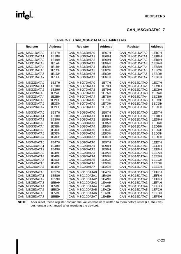
C-23
REGISTERS
CAN_MSGxDATA0–7
Table C-7. CAN_MSGxDATA0–7 Addresses
Register Address Register Address Register Address
CAN_MSG1DATA0CAN_MSG1DATA1CAN_MSG1DATA2CAN_MSG1DATA3CAN_MSG1DATA4CAN_MSG1DATA5CAN_MSG1DATA6CAN_MSG1DATA7
1E17H1E18H1E19H1E1AH1E1BH1E1CH1E1DH1E1EH
CAN_MSG6DATA0CAN_MSG6DATA1CAN_MSG6DATA2CAN_MSG6DATA3CAN_MSG6DATA4CAN_MSG6DATA5CAN_MSG6DATA6CAN_MSG6DATA7
1E67H1E68H1E69H1E6AH1E6BH1E6CH1E6DH1E6EH
CAN_MSG11DATA0CAN_MSG11DATA1CAN_MSG11DATA2CAN_MSG11DATA3CAN_MSG11DATA4CAN_MSG11DATA5CAN_MSG11DATA6CAN_MSG11DATA7
1EB7H1EB8H1EB9H1EBAH1EBBH1EBCH1EBDH1EBEH
CAN_MSG2DATA0CAN_MSG2DATA1CAN_MSG2DATA2CAN_MSG2DATA3CAN_MSG2DATA4CAN_MSG2DATA5CAN_MSG2DATA6CAN_MSG2DATA7
1E27H1E28H1E29H1E2AH1E2BH1E2CH1E2DH1E2EH
CAN_MSG7DATA0CAN_MSG7DATA1CAN_MSG7DATA2CAN_MSG7DATA3CAN_MSG7DATA4CAN_MSG7DATA5CAN_MSG7DATA6CAN_MSG7DATA7
1E77H1E78H1E79H1E7AH1E7BH1E7CH1E7DH1E7EH
CAN_MSG12DATA0CAN_MSG12DATA1CAN_MSG12DATA2CAN_MSG12DATA3CAN_MSG12DATA4CAN_MSG12DATA5CAN_MSG12DATA6CAN_MSG12DATA7
1EC7H1EC8H1EC9H1ECAH1ECBH1ECCH1ECDH1ECEH
CAN_MSG3DATA0CAN_MSG3DATA1CAN_MSG3DATA2CAN_MSG3DATA3CAN_MSG3DATA4CAN_MSG3DATA5CAN_MSG3DATA6CAN_MSG3DATA7
1E37H1E38H1E39H1E3AH1E3BH1E3CH1E3DH1E3EH
CAN_MSG8DATA0CAN_MSG8DATA1CAN_MSG8DATA2CAN_MSG8DATA3CAN_MSG8DATA4CAN_MSG8DATA5CAN_MSG8DATA6CAN_MSG8DATA7
1E87H1E88H1E89H1E8AH1E8BH1E8CH1E8DH1E8EH
CAN_MSG13DATA0CAN_MSG13DATA1CAN_MSG13DATA2CAN_MSG13DATA3CAN_MSG13DATA4CAN_MSG13DATA5CAN_MSG13DATA6CAN_MSG13DATA7
1ED7H1ED8H1ED9H1EDAH1EDBH1EDCH1EDDH1EDEH
CAN_MSG4DATA0CAN_MSG4DATA1CAN_MSG4DATA2CAN_MSG4DATA3CAN_MSG4DATA4CAN_MSG4DATA5CAN_MSG4DATA6CAN_MSG4DATA7
1E47H1E48H1E49H1E4AH1E4BH1E4CH1E4DH1E4EH
CAN_MSG9DATA0CAN_MSG9DATA1CAN_MSG9DATA2CAN_MSG9DATA3CAN_MSG9DATA4CAN_MSG9DATA5CAN_MSG9DATA6CAN_MSG9DATA7
1E97H1E98H1E99H1E9AH1E9BH1E9CH1E9DH1E9EH
CAN_MSG14DATA0CAN_MSG14DATA1CAN_MSG14DATA2CAN_MSG14DATA3CAN_MSG14DATA4CAN_MSG14DATA5CAN_MSG14DATA6CAN_MSG14DATA7
1EE7H1EE8H1EE9H1EEAH1EEBH1EECH1EEDH1EEEH
CAN_MSG5DATA0CAN_MSG5DATA1CAN_MSG5DATA2CAN_MSG5DATA3CAN_MSG5DATA4CAN_MSG5DATA5CAN_MSG5DATA6CAN_MSG5DATA7
1E57H1E58H1E59H1E5AH1E5BH1E5CH1E5DH1E5EH
CAN_MSG10DATA0CAN_MSG10DATA1CAN_MSG10DATA2CAN_MSG10DATA3CAN_MSG10DATA4CAN_MSG10DATA5CAN_MSG10DATA6CAN_MSG10DATA7
1EA7H1EA8H1EA9H1EAAH1EABH1EACH1EADH1EAEH
CAN_MSG15DATA0CAN_MSG15DATA1CAN_MSG15DATA2CAN_MSG15DATA3CAN_MSG15DATA4CAN_MSG15DATA5CAN_MSG15DATA6CAN_MSG15DATA7
1EF7H1EF8H1EF9H1EFAH1EFBH1EFCH1EFDH1EFEH
NOTE: After reset, these register contain the values that were written to them before reset (i.e. their val-ues remain unchanged after resetting the device).

8XC196Kx, Jx, CA USER’S MANUAL
C-24
CAN_MSGxID0–3
CAN_MSGxID0–3x = 1–15 (87C196CA)
Address:Reset State:
Table C-8
Write the message object’s identifier to the CAN message object x identifier (CAN_MSGxID0–3) register. Software can change the identifier during normal operation. Clear the MSGVAL bit in the corresponding CAN_MSGxCON0 register to prevent the CPU from accessing the message object, change the identifier in CAN_MSGxID0–3, then set the MSGVAL bit to allow access.
87C196CA 31 24
CAN_MSGxID3 ID4 ID3 ID2 ID1 ID0 — — —
23 16
CAN_MSGxID2 ID12 ID11 ID10 ID9 ID8 ID7 ID6 ID5
15 8
CAN_MSGxID1 ID20 ID19 ID18 ID17 ID16 ID15 ID14 ID13
7 0
CAN_MSGxID0 ID28 ID27 ID26 ID25 ID24 ID23 ID22 ID21
BitNumber
Bit Mnemonic Function
31:2723:1612:8
ID4:0ID12:5ID17:13
Message Identifier 17:0
These bits hold the 18 least-significant bits of an extended identifier. If you write an extended identifier to these bits, but specify a standard identifier (XTD = 0) in the corresponding message object’s configuration register (CAN_MSGxCFG), the CPU clears these bits (ID17:0).
26:24 — Reserved; for compatibility with future devices, write zeros to these bits.
15:137:0
ID20:18ID28:21
Message Identifier 28:18
These bits hold either an entire standard identifier or the 11 most-significant bits of an extended identifier.
NOTE: This register is the same as the arbitration register in the standalone 82527 CAN peripheral.

C-25
REGISTERS
CAN_MSGxID0–3
Table C-8. CAN_MSGxID0–3 Addresses
Register Address Register Address Register Address
CAN_MSG1ID0CAN_MSG1ID1CAN_MSG1ID2CAN_MSG1ID3
1E12H1E13H1E14H1E15H
CAN_MSG6ID0CAN_MSG6ID1CAN_MSG6ID2CAN_MSG6ID3
1E62H1E63H1E64H1E65H
CAN_MSG11ID0CAN_MSG11ID1CAN_MSG11ID2CAN_MSG11ID3
1EB2H1EB3H1EB4H1EB5H
CAN_MSG2ID0CAN_MSG2ID1CAN_MSG2ID2CAN_MSG2ID3
1E22H1E23H1E24H1E25H
CAN_MSG7ID0CAN_MSG7ID1CAN_MSG7ID2CAN_MSG7ID3
1E72H1E73H1E74H1E75H
CAN_MSG12ID0CAN_MSG12ID1CAN_MSG12ID2CAN_MSG12ID3
1EC2H1EC3H1EC4H1EC5H
CAN_MSG3ID0CAN_MSG3ID1CAN_MSG3ID2CAN_MSG3ID3
1E32H1E33H1E34H1E35H
CAN_MSG8ID0CAN_MSG8ID1CAN_MSG8ID2CAN_MSG8ID3
1E82H1E83H1E84H1E85H
CAN_MSG13ID0CAN_MSG13ID1CAN_MSG13ID2CAN_MSG13ID3
1ED2H1ED3H1ED4H1ED5H
CAN_MSG4ID0CAN_MSG4ID1CAN_MSG4ID2CAN_MSG4ID3
1E42H1E43H1E44H1E45H
CAN_MSG9ID0CAN_MSG9ID1CAN_MSG9ID2CAN_MSG9ID3
1E92H1E93H1E94H1E95H
CAN_MSG14ID0CAN_MSG14ID1CAN_MSG14ID2CAN_MSG14ID3
1EE2H1EE3H1EE4H1EE5H
CAN_MSG5ID0CAN_MSG5ID1CAN_MSG5ID2CAN_MSG5ID3
1E52H1E53H1E54H1E55H
CAN_MSG10ID0CAN_MSG10ID1CAN_MSG10ID2CAN_MSG10ID3
1EA2H1EA3H1EA4H1EA5H
CAN_MSG15ID0CAN_MSG15ID1CAN_MSG15ID2CAN_MSG15ID3
1EF2H1EF3H1EF4H1EF5H
NOTE: After reset, these register contain the values that were written to them before reset.

8XC196Kx, Jx, CA USER’S MANUAL
C-26
CAN_MSK15
CAN_MSK15(87C196CA)
Address:
Reset State:
Table C-9
Program the CAN message 15 mask (CAN_MSK15) register to mask (“don’t care”) specific message identifier bits for message 15 in addition to those bits masked by a global mask (CAN_EGMSK or CAN_SGMSK).
31 24
87C196CA MSK4 MSK3 MSK2 MSK1 MSK0 — — —
23 16
MSK12 MSK11 MSK10 MSK9 MSK8 MSK7 MSK6 MSK5
15 8
MSK20 MSK19 MSK18 MSK17 MSK16 MSK15 MSK14 MSK13
7 0
MSK28 MSK27 MSK26 MSK25 MSK24 MSK23 MSK22 MSK21
BitNumber Function
31:27 MSK4:0 ID Mask
These bits individually mask incoming message identifier (ID) bits.
0 = mask the ID bit (accept either “0” or “1”)1 = accept only an exact match
26:24 — Reserved. These bits are undefined; for compatibility with future devices, do not modify these bits.
23:1615:87:0
MSK12:5MSK20:13MSK28:21
ID Mask
These bits individually mask incoming message identifier (ID) bits.
0 = mask the ID bit (accept either “0” or “1”)1 = accept only an exact match
NOTE: Setting a CAN_MSK15 bit in any position that is cleared in the global mask register has noeffect. The message 15 mask is ANDed with the global mask, so any “don’t care” bitsdefined in a global mask are also “don’t care” bits for message 15.
Table C-9. CAN_MSK15 Addresses and Reset Values
Register Address Reset Value
CAN_MSK15 (bits 0–7) 1E0CH Unchanged††
CAN_MSK15 (bits 8–15) 1E0DH Unchanged
CAN_MSK15 (bits 16–23) 1E0EH Unchanged
CAN_MSK15 (bits 24–31) 1E0FH Unchanged
† This register can be accessed as a byte, word, or double word.†† After reset, this register contains the value that was written to it before reset.
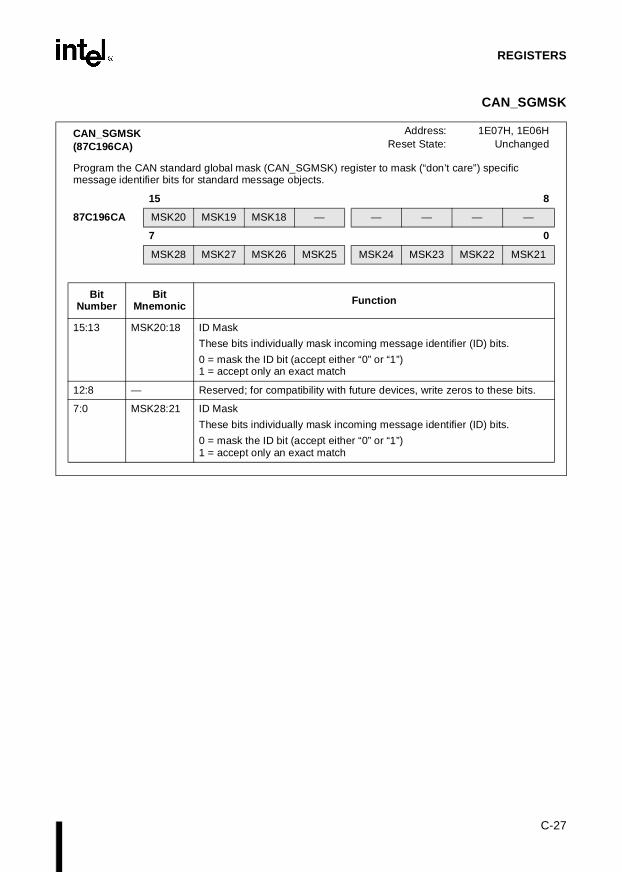
C-27
REGISTERS
CAN_SGMSK
CAN_SGMSK(87C196CA)
Address:Reset State:
1E07H, 1E06HUnchanged
Program the CAN standard global mask (CAN_SGMSK) register to mask (“don’t care”) specific message identifier bits for standard message objects.
15 8
87C196CA MSK20 MSK19 MSK18 — — — — —
7 0
MSK28 MSK27 MSK26 MSK25 MSK24 MSK23 MSK22 MSK21
BitNumber
Bit Mnemonic Function
15:13 MSK20:18 ID Mask
These bits individually mask incoming message identifier (ID) bits.
0 = mask the ID bit (accept either “0” or “1”)1 = accept only an exact match
12:8 — Reserved; for compatibility with future devices, write zeros to these bits.
7:0 MSK28:21 ID Mask
These bits individually mask incoming message identifier (ID) bits.
0 = mask the ID bit (accept either “0” or “1”)1 = accept only an exact match
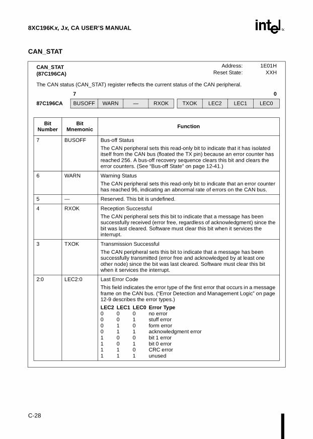
8XC196Kx, Jx, CA USER’S MANUAL
C-28
CAN_STAT
CAN_STAT(87C196CA)
Address:Reset State:
1E01HXXH
The CAN status (CAN_STAT) register reflects the current status of the CAN peripheral.
7 0
87C196CA BUSOFF WARN — RXOK TXOK LEC2 LEC1 LEC0
BitNumber
BitMnemonic Function
7 BUSOFF Bus-off Status
The CAN peripheral sets this read-only bit to indicate that it has isolated itself from the CAN bus (floated the TX pin) because an error counter has reached 256. A bus-off recovery sequence clears this bit and clears the error counters. (See “Bus-off State” on page 12-41.)
6 WARN Warning Status
The CAN peripheral sets this read-only bit to indicate that an error counter has reached 96, indicating an abnormal rate of errors on the CAN bus.
5 — Reserved. This bit is undefined.
4 RXOK Reception Successful
The CAN peripheral sets this bit to indicate that a message has been successfully received (error free, regardless of acknowledgment) since the bit was last cleared. Software must clear this bit when it services the interrupt.
3 TXOK Transmission Successful
The CAN peripheral sets this bit to indicate that a message has been successfully transmitted (error free and acknowledged by at least one other node) since the bit was last cleared. Software must clear this bit when it services the interrupt.
2:0 LEC2:0 Last Error Code
This field indicates the error type of the first error that occurs in a message frame on the CAN bus. (“Error Detection and Management Logic” on page 12-9 describes the error types.)
LEC2 LEC1 LEC0 Error Type0 0 0 no error0 0 1 stuff error0 1 0 form error0 1 1 acknowledgment error1 0 0 bit 1 error1 0 1 bit 0 error1 1 0 CRC error1 1 1 unused

C-29
REGISTERS
CCR0
CCR0 Address:Reset State:
2018HXXH
The chip configuration 0 (CCR0) register controls powerdown mode, bus-control signals, and internal memory protection. Three of its bits combine with two bits of CCR1 to control wait states and bus width.
7 0
LOC1 LOC0 IRC1 IRC0 ALE WR BW0 PD
Bit Number
Bit Mnemonic Function
7:6 LOC1:0 Lock Bits
Determine the programming protection scheme for internal memory.
LOC1 LOC0
0 0 read and write protect0 1 read protect only1 0 write protect only1 1 no protection
5:4 IRC1:0 Internal Ready Control
These two bits, along with IRC2 (CCR1.1), limit the number of wait states that can be inserted while the READY pin is held low. Wait states are inserted into the bus cycle either until the READY pin is pulled high or until this internal number is reached.
IRC2 IRC1 IRC0
0 0 0 zero wait states0 X 1 illegal0 1 X illegal1 0 0 one wait state1 0 1 two wait states1 1 0 three wait states1 1 1 infinite†
† This mode is unavailable on the 8XC196Jx device. On this device, the READY pin is not implemented. Therefore, the number of wait states inserted into the bus cycle is determined only by the IRC2:0 bit settings.
3 ALE Address Valid Strobe and Write Strobe
These bits define which bus-control signals will be generated during external read and write cycles.
ALE WR
0 0 address valid with write strobe mode(ADV#, RD#, WRL#, WRH#)†
0 1 address valid strobe mode(ADV#, RD#, WR#, BHE#)†
1 0 write strobe mode(ALE, RD#, WRL#, WRH#)†
1 1 standard bus-control mode(ALE, RD#, WR#, BHE#)†
† On the 8XC196Jx device, the BHE#/WRH# pin is not implemented.
2 WR

8XC196Kx, Jx, CA USER’S MANUAL
C-30
CCR0
1 BW0 Buswidth Control
This bit, along with the BW1 bit (CCR1.2), selects the bus width.
BW1 BW0
0 0 illegal0 1 16-bit only1 0 8-bit only1 1 BUSWIDTH pin controlled†
† This mode is unavailable on the 87C196CA, Jx devices. The BUSWIDTH pin is not implemented.
0 PD Powerdown Enable
Controls whether the IDLPD #2 instruction causes the device to enter powerdown mode. Clearing this bit at reset can prevent accidental entry into powerdown mode.
1 = enable powerdown mode0 = disable powerdown mode
CCR0 (Continued) Address:Reset State:
2018HXXH
The chip configuration 0 (CCR0) register controls powerdown mode, bus-control signals, and internal memory protection. Three of its bits combine with two bits of CCR1 to control wait states and bus width.
7 0
LOC1 LOC0 IRC1 IRC0 ALE WR BW0 PD
Bit Number
Bit Mnemonic Function
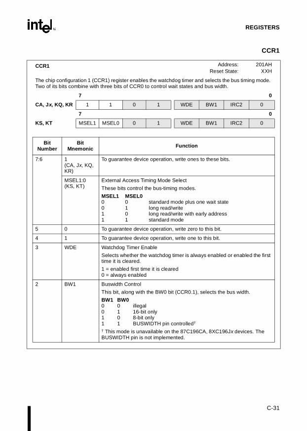
C-31
REGISTERS
CCR1
CCR1 Address:Reset State:
201AHXXH
The chip configuration 1 (CCR1) register enables the watchdog timer and selects the bus timing mode. Two of its bits combine with three bits of CCR0 to control wait states and bus width.
7 0
CA, Jx, KQ, KR 1 1 0 1 WDE BW1 IRC2 0
7 0
KS, KT MSEL1 MSEL0 0 1 WDE BW1 IRC2 0
BitNumber
BitMnemonic Function
7:6 1(CA, Jx, KQ, KR)
To guarantee device operation, write ones to these bits.
MSEL1:0(KS, KT)
External Access Timing Mode Select
These bits control the bus-timing modes.
MSEL1 MSEL00 0 standard mode plus one wait state0 1 long read/write1 0 long read/write with early address1 1 standard mode
5 0 To guarantee device operation, write zero to this bit.
4 1 To guarantee device operation, write one to this bit.
3 WDE Watchdog Timer Enable
Selects whether the watchdog timer is always enabled or enabled the first time it is cleared.
1 = enabled first time it is cleared0 = always enabled
2 BW1 Buswidth Control
This bit, along with the BW0 bit (CCR0.1), selects the bus width.
BW1 BW00 0 illegal0 1 16-bit only1 0 8-bit only1 1 BUSWIDTH pin controlled†
† This mode is unavailable on the 87C196CA, 8XC196Jx devices. The BUSWIDTH pin is not implemented.

8XC196Kx, Jx, CA USER’S MANUAL
C-32
CCR1
1 IRC2 Ready Control
This bit, along with IRC0 (CCR0.4) and IRC1 (CCR0.5), limits the number of wait states that can be inserted while the READY pin is held low. Wait states are inserted into the bus cycle either until the READY pin is pulled high or until this internal number is reached.
IRC2 IRC1 IRC00 0 0 zero wait states0 X 1 illegal0 1 X illegal1 0 0 one wait state1 0 1 two wait states1 1 0 three wait states1 1 1 infinite†
† This mode is unavailable on the 8XC196Jx device. On this device, the READY pin is not implemented. Therefore, the number of wait states inserted into the bus cycle is determined only by the IRC2:0 bit settings.
0 — Reserved; always write as zero.
CCR1 (Cont inued) Address:Reset State:
201AHXXH
The chip configuration 1 (CCR1) register enables the watchdog timer and selects the bus timing mode. Two of its bits combine with three bits of CCR0 to control wait states and bus width.
7 0
CA, Jx, KQ, KR 1 1 0 1 WDE BW1 IRC2 0
7 0
KS, KT MSEL1 MSEL0 0 1 WDE BW1 IRC2 0
BitNumber
BitMnemonic Function

C-33
REGISTERS
COMPx_CON
COMPx_CON x = 0–1
Address:Reset State:
Table C-10
The EPA compare control (COMPx_CON) registers determine the function of the EPA compare channels.
7 0
TB CE M1 M0 RE AD ROT RT
Bit Number
Bit Mnemonic Function
7 TB Time Base Select
Specifies the reference timer.
1 = timer 2 is the reference timer and timer 1 is the opposite timer0 = timer 1 is the reference timer and timer 2 is the opposite timer
A compare event (start of an A/D conversion; clearing, setting, or toggling an output pin; and/or resetting either timer) occurs when the reference timer matches the time programmed in the event-time register.
6 CE Compare Enable
This bit enables the compare function.
1 = compare function enabled0 = compare function disabled
5:4 M1:0 EPA Mode Select
Specifies the type of compare event.
M1 M0
0 0 no output0 1 clear output pin1 0 set output pin1 1 toggle output pin
3 RE Re-enable
Allows a compare event to continue to execute each time the event-time register (COMPx_TIME) matches the reference timer rather than only upon the first time match.
1 = compare function always enabled0 = compare function will drive the output only once.
2 AD A/D Conversion
Allows the EPA to start an A/D conversion that has been previously set up in the A/D control registers. To use this feature, you must select the EPA as the conversion source in the AD_CONTROL register.
1 = EPA compare event triggers an A/D conversion0 = causes no A/D action

8XC196Kx, Jx, CA USER’S MANUAL
C-34
COMPx_CON
1 ROT Reset Opposite Timer and Reset Timer
These bits control whether an EPA compare event resets the reference timer or the opposite timer.
ROT RTX 0 reset function disabled0 1 resets reference timer1 1 resets opposite timer
The state of the TB bit (COMPx_CON.7) determines which timer is the reference timer and which timer is the opposite timer.
0 RT Reset Timer
This bit controls whether the timer selected by the ROT bit will be reset
1 = resets the timer selected by the ROT bit0 = disables the reset function
Table C-10. COMPx_CON Addresses and Reset Values
Register Address Reset Value
COMP0_CON 1F88H 00H
COMP1_CON 1F8CH 00H
COMPx_CON (Continued)
Address:Reset State:
Table C-10
The EPA compare control (COMPx_CON) registers determine the function of the EPA compare channels.
7 0
TB CE M1 M0 RE AD ROT RT
Bit Number
Bit Mnemonic Function
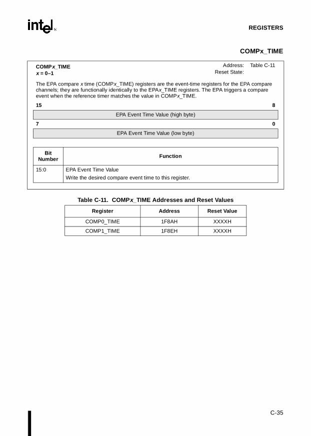
C-35
REGISTERS
COMPx_TIME
COMPx_TIMEx = 0–1
Address:Reset State:
Table C-11
The EPA compare x time (COMPx_TIME) registers are the event-time registers for the EPA compare channels; they are functionally identically to the EPAx_TIME registers. The EPA triggers a compare event when the reference timer matches the value in COMPx_TIME.
15 8
EPA Event Time Value (high byte)
7 0
EPA Event Time Value (low byte)
Bit Number Function
15:0 EPA Event Time Value
Write the desired compare event time to this register.
Table C-11. COMPx_TIME Addresses and Reset Values
Register Address Reset Value
COMP0_TIME 1F8AH XXXXH
COMP1_TIME 1F8EH XXXXH

8XC196Kx, Jx, CA USER’S MANUAL
C-36
EPA_MASK
EPA_MASK Address:Reset State:
1FA0H0000H
The EPA interrupt mask (EPA_MASK) register enables or disables (masks) interrupts associated with the multiplexed EPAx interrupt.
15 8
CA, Jx — — — — EPA8 EPA9 OVR0 OVR1
7 0
0VR2 OVR3 — — — — OVR8 OVR9
15 8
Kx EPA4 EPA5 EPA6 EPA7 EPA8 EPA9 OVR0 OVR1
7 0
OVR2 OVR3 OVR4 OVR5 OVR6 OVR7 OVR8 OVR9
BitNumber Function
15:0† Setting a bit enables the corresponding interrupt as a multiplexed EPAx interrupt source. The multiplexed EPAx interrupt is enabled by setting its interrupt enable bit in the interrupt mask register (INT_MASK.0 = 1).
† Bits 2–5 and 12–15 are reserved on the 8XC196CA, Jx devices. For compatibility with future devices, write zeros to these bits.

C-37
REGISTERS
EPA_MASK1
EPA_MASK1 Address:Reset State:
1FA4H00H
The EPA interrupt mask 1 (EPA_MASK1) register enables or disables (masks) interrupts associated with the EPAx interrupt.
7 0
— — — — COMP0 COMP1 OVRTM1 OVRTM2
Bit Number Function
7:4 Reserved; for compatibility with future devices, write zeros to these bits.
3:0 Setting a bit enables the corresponding interrupt as a multiplexed EPAx interrupt source. The multiplexed EPAx interrupt is enabled by setting its interrupt enable bit in the interrupt mask register (INT_MASK.0 = 1).

8XC196Kx, Jx, CA USER’S MANUAL
C-38
EPA_PEND
EPA_PEND Address:Reset State:
1FA2H0000H
When hardware detects a pending EPAx interrupt, it sets the corresponding bit in EPA interrupt pending (EPA_PEND or EPA_PEND1) registers. The EPAIPV register contains a number that identifies the highest priority, active, multiplexed interrupt source. When EPAIPV is read, the EPA interrupt pending bit associated with the EPAIPV priority value is cleared.
15 8
CA, Jx — — — — EPA8 EPA9 OVR0 OVR1
7 0
OVR2 OVR3 — — — — OVR8 OVR9
15 8
Kx EPA4 EPA5 EPA6 EPA7 EPA8 EPA9 OVR0 OVR1
7 0
OVR2 OVR3 OVR4 OVR5 OVR6 OVR7 OVR8 OVR9
BitNumber Function
15:0† Any set bit indicates that the corresponding EPAx interrupt source is pending. The bit is cleared when the EPA interrupt priority vector register (EPAIPV) is read.
† Bits 2–5 and 12–15 are reserved on the 8XC196CA, Jx devices. For compatibility with future devices, write zeros to these bits.

C-39
REGISTERS
EPA_PEND1
EPA_PEND1 Address:Reset State:
1FA6H00H
When hardware detects a pending EPAx interrupt, it sets the corresponding bit in EPA interrupt pending (EPA_PEND or EPA_PEND1) registers. The EPAIPV register contains a number that identifies the highest priority, active, multiplexed interrupt source. When EPAIPV is read, the EPA interrupt pending bit associated with the EPAIPV priority value is cleared.
7 0
— — — — COMP0 COMP1 OVRTM1 OVRTM2
Bit Number Function
7:4 Reserved; always write as zeros.
3:0 Any set bit indicates that the corresponding EPAx interrupt source is pending. The bit is cleared when the EPA interrupt priority vector register (EPAIPV) is read.

8XC196Kx, Jx, CA USER’S MANUAL
C-40
EPAx_CON
EPAx_CON x = 0–9 (8XC196Kx)x = 0–3, 8, 9 (8XC196CA, Jx)
Address:Reset State:
Table C-12
The EPA control (EPAx_CON) registers control the functions of their assigned capture/compare channels. The registers for EPA0, EPA2, and EPA4–9 are identical. The registers for EPA1 and EPA3 have an additional bit, the remap bit. This added bit (bit 8) requires an additional byte, so EPA1_CON and EPA3_CON must be addressed as words, while the others can be addressed as bytes.
15 8
x = 1, 3 — — — — — — — RM
7 0
TB CE M1 M0 RE AD ROT ON/RT
7 0
x = 0, 2, 4–9 TB CE M1 M0 RE AD ROT ON/RT
BitNumber
Bit Mnemonic Function
15:9† — Reserved; always write as zeros.
8† RM Remap Feature
The Remap feature applies to the compare mode of the EPA1 and EPA3 only.
When the remap feature of EPA1 is enabled, EPA capture/compare channel 0 shares output pin EPA1 with EPA capture/compare channel 1. When the remap feature of EPA3 is enabled, EPA capture/compare channel 2 shares output pin EPA3 with EPA capture/compare channel 3.
0 = remap feature disabled1 = remap feature enabled
7 TB Time Base Select
Specifies the reference timer.
0 = Timer 1 is the reference timer and Timer 2 is the opposite timer1 = Timer 2 is the reference timer and Timer 1 is the opposite timer
A compare event (start of an A/D conversion; clearing, setting, or toggling an output pin; and/or resetting either timer) occurs when the reference timer matches the time programmed in the event-time register.
When a capture event (falling edge, rising edge, or an edge change on the EPAx pin) occurs, the reference timer value is saved in the EPA event-time register (EPAx_TIME).
6 CE Compare Enable
Determines whether the EPA channel operates in capture or compare mode.
0 = capture mode1 = compare mode
† These bits apply to the EPA1_CON and EPA3_CON registers only.

C-41
REGISTERS
EPAx_CON
5:4 M1:0 EPA Mode Select
In capture mode, specifies the type of event that triggers an input capture. In compare mode, specifies the action that the EPA executes when the reference timer matches the event time.
M1 M0 Capture Mode Event
0 0 no capture0 1 capture on falling edge1 0 capture on rising edge1 1 capture on either edge
M1 M0 Compare Mode Action
0 0 no output0 1 clear output pin1 0 set output pin1 1 toggle output pin
3 RE Re-enable
Re-enable applies to the compare mode only. It allows a compare event to continue to execute each time the event-time register (EPAx_TIME) matches the reference timer rather than only upon the first time match.
0 = compare function is disabled after a single event1 = compare function always enabled
2 AD A/D Conversion
Allows the EPA to start an A/D conversion that has been previously set up in the A/D control registers. To use this feature, you must select the EPA as the conversion source in the AD_CONTROL register.
0 = causes no A/D action1 = EPA capture or compare event triggers an A/D conversion
EPAx_CON (Continued)x = 0–9 (8XC196Kx)x = 0–3, 8, 9 (8XC196CA, Jx)
Address:Reset State:
Table C-12
The EPA control (EPAx_CON) registers control the functions of their assigned capture/compare channels. The registers for EPA0, EPA2, and EPA4–9 are identical. The registers for EPA1 and EPA3 have an additional bit, the remap bit. This added bit (bit 8) requires an additional byte, so EPA1_CON and EPA3_CON must be addressed as words, while the others can be addressed as bytes.
15 8
x = 1, 3 — — — — — — — RM
7 0
TB CE M1 M0 RE AD ROT ON/RT
7 0
x = 0, 2, 4–9 TB CE M1 M0 RE AD ROT ON/RT
BitNumber
Bit Mnemonic Function
† These bits apply to the EPA1_CON and EPA3_CON registers only.

8XC196Kx, Jx, CA USER’S MANUAL
C-42
EPAx_CON
1 ROT Reset Opposite Timer
Controls different functions for capture and compare modes.
In Capture Mode:
0 = causes no action1 = resets the opposite timer
In Compare Mode:
ROT selects the timer that is to be reset if the RT bit is set:
0 = selects base timer1 = selects opposite timer
The TB bit (bit 7) selects which timer is the reference timer and which timer is the opposite timer.
0 ON/RT Overwrite New/Reset Timer
The ON/RT bit functions as overwrite new in capture mode and reset timer in compare mode.
In Capture Mode (ON):
An overrun error is generated when an input capture occurs while the event-time register (EPAx_TIME) and its buffer are both full. When an overrun occurs, the ON bit determines whether old data is overwritten or new data is ignored:
0 = ignores new data1 = overwrites old data in the buffer
In Compare Mode (RT):
0 = disables the reset function1 = resets the ROT-selected timer
EPAx_CON (Continued)x = 0–9 (8XC196Kx)x = 0–3, 8, 9 (8XC196CA, Jx)
Address:Reset State:
Table C-12
The EPA control (EPAx_CON) registers control the functions of their assigned capture/compare channels. The registers for EPA0, EPA2, and EPA4–9 are identical. The registers for EPA1 and EPA3 have an additional bit, the remap bit. This added bit (bit 8) requires an additional byte, so EPA1_CON and EPA3_CON must be addressed as words, while the others can be addressed as bytes.
15 8
x = 1, 3 — — — — — — — RM
7 0
TB CE M1 M0 RE AD ROT ON/RT
7 0
x = 0, 2, 4–9 TB CE M1 M0 RE AD ROT ON/RT
BitNumber
Bit Mnemonic Function
† These bits apply to the EPA1_CON and EPA3_CON registers only.
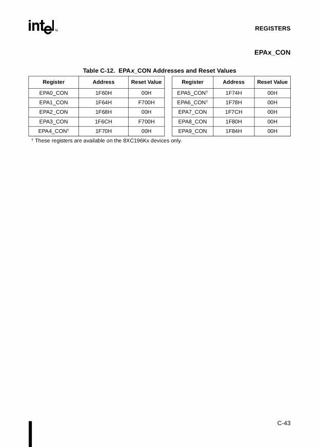
C-43
REGISTERS
EPAx_CON
Table C-12. EPA x_CON Addresses and Reset Values
Register Address Reset Value Register Address Reset Value
EPA0_CON 1F60H 00H EPA5_CON† 1F74H 00H
EPA1_CON 1F64H F700H EPA6_CON† 1F78H 00H
EPA2_CON 1F68H 00H EPA7_CON 1F7CH 00H
EPA3_CON 1F6CH F700H EPA8_CON 1F80H 00H
EPA4_CON† 1F70H 00H EPA9_CON 1F84H 00H
† These registers are available on the 8XC196Kx devices only.

8XC196Kx, Jx, CA USER’S MANUAL
C-44
EPAx_TIME
EPAx_TIMEx = 0–9 (8XC196Kx)x = 0–3, 8, 9 (87C196CA, 8XC196Jx)
Address:Reset State:
Table C-13
The EPA time (EPAx_TIME) registers are the event-time registers for the EPA channels. In capture mode, the value of the reference timer is captured in EPAx_TIME when an input transition occurs. Each event-time register is buffered, allowing the storage of two capture events at once. In compare mode, the EPA triggers a compare event when the reference timer matches the value in EPAx_TIME. EPAx_TIME is not buffered for compare mode.
15 8
EPA Timer Value (high byte)
7 0
EPA Timer Value (low byte)
Bit Number Function
15:0 EPA Time Value
When an EPA channel is configured for capture mode, this register contains the value of the reference timer when the specified event occurred.
When an EPA channel is configured for compare mode, write the compare event time to this register.
Table C-13. EPA x_TIME Addresses and Reset Values
Register Address Reset Value Register Address Reset Value
EPA0_TIME 1F62H XXXXH EPA5_TIME† 1F76H XXXXH
EPA1_TIME 1F66H XXXXH EPA6_TIME† 1F7AH XXXXH
EPA2_TIME 1F6AH XXXXH EPA7_TIME† 1F7EH XXXXH
EPA3_TIME 1F6EH XXXXH EPA8_TIME 1F82H XXXXH
EPA4_TIME† 1F72H XXXXH EPA9_TIME 1F86H XXXXH
† These registers are available on the 8XC196Kx devices only.
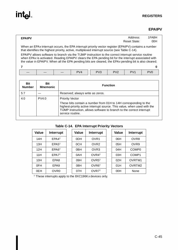
C-45
REGISTERS
EPAIPV
EPAIPV Address:Reset State:
1FA8H00H
When an EPAx interrupt occurs, the EPA interrupt priority vector register (EPAIPV) contains a number that identifies the highest priority, active, multiplexed interrupt source (see Table C-14).
EPAIPV allows software to branch via the TIJMP instruction to the correct interrupt service routine when EPAx is activated. Reading EPAIPV clears the EPA pending bit for the interrupt associated with the value in EPAIPV. When all the EPA pending bits are cleared, the EPAx pending bit is also cleared.
7 0
— — — PV4 PV3 PV2 PV1 PV0
Bit Number
Bit Mnemonic Function
5:7 — Reserved; always write as zeros.
4:0 PV4:0 Priority Vector
These bits contain a number from 01H to 14H corresponding to the highest-priority active interrupt source. This value, when used with the TIJMP instruction, allows software to branch to the correct interrupt service routine.
Table C-14. EPA Interrupt Priority Vectors
Value Interrupt Value Interrupt Value Interrupt
14H EPA4† 0DH OVR1 06H OVR8
13H EPA5† 0CH OVR2 05H OVR9
12H EPA6† 0BH OVR3 04H COMP0
11H EPA7† 0AH OVR4† 03H COMP1
10H EPA8 09H OVR5† 02H OVRTM1
0FH EPA9 08H OVR6† 01H OVRTM2
0EH OVR0 07H OVR7† 00H None
† These interrupts apply to the 8XC196Kx devices only.

8XC196Kx, Jx, CA USER’S MANUAL
C-46
INT_MASK
INT_MASK Address:Reset State:
08H00H
The interrupt mask (INT_MASK) register enables or disables (masks) individual interrupts. (The EI and DI instructions enable and disable servicing of all maskable interrupts.). INT_MASK is the low byte of the program status word (PSW). PUSHF or PUSHA saves the contents of this register onto the stack and then clears this register. Interrupt calls cannot occur immediately following this instruction. POPF or POPA restores it.
7 0
CA, Jx — — AD EPA0 EPA1 EPA2 EPA3 EPAx
7 0
8XC196Kx IBF OBE AD EPA0 EPA1 EPA2 EPA3 EPAx
BitNumber Function
7:0† Setting this bit enables the corresponding interrupt.
The standard interrupt vector locations are as follows:
Bit Mnemonic Interrupt Standard VectorIBF (Kx) Slave Port Input Buffer Full 200EHOBE (Kx) Slave Port Output Buffer Empty 200CHAD A/D Conversion Complete 200AHEPA0 EPA Capture/Compare Channel 0 2008HEPA1 EPA Capture/Compare Channel 1 2006HEPA2 EPA Capture/Compare Channel 2 2004HEPA3 EPA Capture/Compare Channel 3 2002HEPAx†† Multiplexed EPA 2000H
†† EPA 4–9 capture/compare channel events, EPA 0–1 compare channel events, EPA 0–9 capture/compare overruns, and timer overflows can generate this multiplexed interrupt. The EPA mask and pending registers decode the EPAx interrupt. Write the EPA mask registers (EPA_MASK and EPA_MASK1) to enable the interrupt sources; read the EPA pending registers (EPA_PEND and EPA_PEND1) to determine which source caused the interrupt.
† Bits 6–7 are reserved on the 87C196CA and 8XC196Jx devices. For compatibility with future devices, write zeros to these bits.

C-47
REGISTERS
INT_MASK1
INT_MASK1 Address:Reset State:
13H00H
The interrupt mask 1 (INT_MASK1) register enables or disables (masks) individual interrupts. (The EI and DI instructions enable and disable servicing of all maskable interrupts.) INT_MASK1 can be read from or written to as a byte register. PUSHA saves this register on the stack and POPA restores it.
7 0
87C196CA NMI EXTINT CAN RI TI SSIO1 SSIO0 —
7 0
8XC196Jx — EXTINT — RI TI SSIO1 SSIO0 —
7 0
8XC196Kx NMI EXTINT — RI TI SSIO1 SSIO0 CBF
BitNumber Function
7:0† Setting this bit enables the corresponding interrupt.
The standard interrupt vector locations are as follows:
Bit Mnemonic Interrupt Standard VectorNMI†† Nonmaskable Interrupt 203EHEXTINT EXTINT Pin 203CHCAN (CA) CAN Peripheral 203AHRI SIO Receive 2038HTI SIO Transmit 2036HSSIO1 SSIO 1 Transfer 2034HSSIO0 SSIO 0 Transfer 2032HCBF (Kx) Slave Port Command Buffer Full 2030H
† Bit 5 is reserved on the 8XC196Jx, Kx devices and bit 0 is reserved on the 87C196CA, 8XC196Jx devices. For compatibility with future devices, always write zeros to these bits.†† NMI is always enabled. This nonfunctional mask bit exists for design symmetry with the INT_PEND1 register. Always write zero to this bit.

8XC196Kx, Jx, CA USER’S MANUAL
C-48
INT_PEND
INT_PEND Address:Reset State:
09H00H
When hardware detects an interrupt request, it sets the corresponding bit in the interrupt pending (INT_PEND or INT_PEND1) registers. When the vector is taken, the hardware clears the pending bit. Software can generate an interrupt by setting the corresponding interrupt pending bit.
7 0
CA, Jx — — AD EPA0 EPA1 EPA2 EPA3 EPAx
7 0
8XC196Kx IBF OBE AD EPA0 EPA1 EPA2 EPA3 EPAx
BitNumber Function
7:0† When set, this bit indicates that the corresponding interrupt is pending. The interrupt bit is cleared when processing transfers to the corresponding interrupt vector.
The standard interrupt vector locations are as follows:
Bit Mnemonic Interrupt Standard VectorIBF (Kx) Slave Port Input Buffer Full 200EHOBE (Kx) Slave Port Output Buffer Empty 200CHAD A/D Conversion Complete 200AHEPA0 EPA Capture/Compare Channel 0 2008HEPA1 EPA Capture/Compare Channel 1 2006HEPA2 EPA Capture/Compare Channel 2 2004HEPA3 EPA Capture/Compare Channel 3 2002HEPAx†† Multiplexed EPA 2000H
†† EPA 4–9 capture/compare channel events, EPA 0–1 compare channel events, EPA 0–9 capture/compare overruns, and timer overflows can generate this multiplexed interrupt. The EPA mask and pending registers decode the EPAx interrupt. Write the EPA mask registers to enable the interrupt sources; read the EPA pending registers (EPA_PEND and EPA_PEND1) to determine which source caused the interrupt.
† Bits 6–7 are reserved on the 87C196CA, 8XC196Jx devices. For compatibility with future devices, write zeros to these bits.
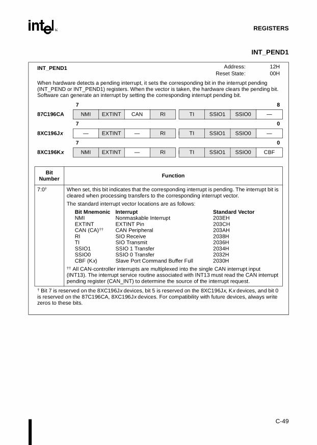
C-49
REGISTERS
INT_PEND1
INT_PEND1 Address:Reset State:
12H00H
When hardware detects a pending interrupt, it sets the corresponding bit in the interrupt pending (INT_PEND or INT_PEND1) registers. When the vector is taken, the hardware clears the pending bit. Software can generate an interrupt by setting the corresponding interrupt pending bit.
7 8
87C196CA NMI EXTINT CAN RI TI SSIO1 SSIO0 —
7 0
8XC196Jx — EXTINT — RI I TI SSIO1 SSIO0 —
7 0
8XC196Kx NMI EXTINT — RI I TI SSIO1 SSIO0 CBF
BitNumber Function
7:0† When set, this bit indicates that the corresponding interrupt is pending. The interrupt bit is cleared when processing transfers to the corresponding interrupt vector.
The standard interrupt vector locations are as follows:
Bit Mnemonic Interrupt Standard VectorNMI Nonmaskable Interrupt 203EHEXTINT EXTINT Pin 203CHCAN (CA)†† CAN Peripheral 203AHRI SIO Receive 2038HTI SIO Transmit 2036HSSIO1 SSIO 1 Transfer 2034HSSIO0 SSIO 0 Transfer 2032HCBF (Kx) Slave Port Command Buffer Full 2030H
†† All CAN-controller interrupts are multiplexed into the single CAN interrupt input (INT13). The interrupt service routine associated with INT13 must read the CAN interrupt pending register (CAN_INT) to determine the source of the interrupt request.
† Bit 7 is reserved on the 8XC196Jx devices, bit 5 is reserved on the 8XC196Jx, Kx devices, and bit 0 is reserved on the 87C196CA, 8XC196Jx devices. For compatibility with future devices, always write zeros to these bits.
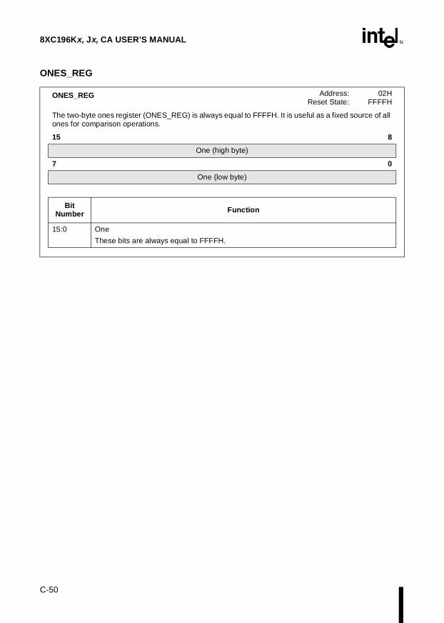
8XC196Kx, Jx, CA USER’S MANUAL
C-50
ONES_REG
ONES_REG Address:Reset State:
02HFFFFH
The two-byte ones register (ONES_REG) is always equal to FFFFH. It is useful as a fixed source of all ones for comparison operations.
15 8
One (high byte)
7 0
One (low byte)
Bit Number Function
15:0 One
These bits are always equal to FFFFH.

C-51
REGISTERS
Px_DIR
Px_DIR x = 1, 2, 5, 6
Address:Reset State:
Table C-15
Each pin of port x can operate in any of the standard I/O modes of operation: complementary output, open-drain output, or high-impedance input. The port x I/O direction (Px_DIR) register determines the I/O mode for each port x pin. The register settings for an open-drain output or a high-impedance input are identical. An open-drain output configuration requires an external pull-up. A high-impedance input configuration requires that the corresponding bit in Px_REG be set.
7 0
x = 1 (CA, Jx) — — — — PIN3 PIN2 PIN1 PIN0
7 0
x = 2 (CA, Jx) PIN7 PIN6 — PIN4 — PIN2 PIN1 PIN0
7 0
x = 5 (CA) — PIN6 PIN5 PIN4 PIN3 PIN2 — PIN0
7 0
x = 5 (Jx) — — — — PIN3 PIN2 — PIN0
7 0
x = 6 (CA, Jx) PIN7 PIN6 PIN5 PIN4 — — PIN1 PIN0
7 0
x = 1, 2, 5, 6 (Kx) PIN7 PIN6 PIN5 PIN4 PIN3 PIN2 PIN1 PIN0
BitNumber
BitMnemonic Function
7:0 PIN7:0 Port x Pin y Direction
This bit selects the Px.y direction:
1 = input/open-drain output (input, output, or bidirectional)0 = complementary output (output only)
Table C-15. Px_DIR Addresses and Reset Values
Register Address Reset Value
P1_DIR 1FD2H FFH
P2_DIR 1FCBH 7FH
P5_DIR 1FF3H FFH
P6_DIR 1FD3H FFH

8XC196Kx, Jx, CA USER’S MANUAL
C-52
Px_MODE
Px_MODE x = 1, 2, 5, 6
Address:Reset State:
Table C-16
Each bit in the port x mode (Px_MODE) register determines whether the corresponding pin functions as a standard I/O port pin or is used for a special-function signal.
7 0
x = 1 (CA, Jx) — — — — PIN3 PIN2 PIN1 PIN0
7 0
x = 2 (CA, Jx) PIN7 PIN6 — PIN4 — PIN2 PIN1 PIN0
7 0
x = 5 (CA) — PIN6 PIN5 PIN4 PIN3 PIN2 — PIN0
7 0
x = 5 (Jx) — — — — PIN3 PIN2 — PIN0
7 0
x = 6 (CA, Jx) PIN7 PIN6 PIN5 PIN4 — — PIN1 PIN0
7 0
x = 1, 2, 5, 6 (Kx) PIN7 PIN6 PIN5 PIN4 PIN3 PIN2 PIN1 PIN0
BitNumber
BitMnemonic Function
7:0 PIN7:0 Port x Pin y Mode
This bit determines the mode of the corresponding port pin:
0 = standard I/O port pin1 = special-function signal
Table C-17 lists the special-function signals for each pin.
Table C-16. Px_MODE Addresses and Reset Values
Register Address Reset Value
P1_MODE 1FD0H 00H
P2_MODE 1FC9H 80H
P5_MODE 1FF1H 80H
P6_MODE 1FD1H 00H
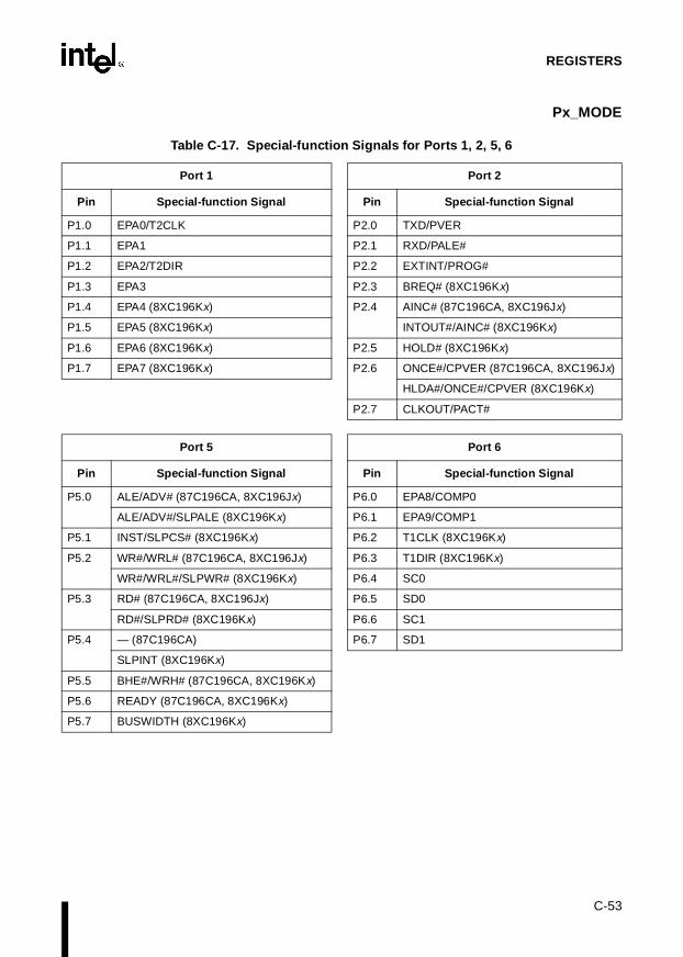
C-53
REGISTERS
Px_MODE
Table C-17. Special-function Signals for Ports 1, 2, 5, 6
Port 1 Port 2
Pin Special-function Signal Pin Special-function Signal
P1.0 EPA0/T2CLK P2.0 TXD/PVER
P1.1 EPA1 P2.1 RXD/PALE#
P1.2 EPA2/T2DIR P2.2 EXTINT/PROG#
P1.3 EPA3 P2.3 BREQ# (8XC196Kx)
P1.4 EPA4 (8XC196Kx) P2.4 AINC# (87C196CA, 8XC196Jx)
P1.5 EPA5 (8XC196Kx) INTOUT#/AINC# (8XC196Kx)
P1.6 EPA6 (8XC196Kx) P2.5 HOLD# (8XC196Kx)
P1.7 EPA7 (8XC196Kx) P2.6 ONCE#/CPVER (87C196CA, 8XC196Jx)
HLDA#/ONCE#/CPVER (8XC196Kx)
P2.7 CLKOUT/PACT#
Port 5 Port 6
Pin Special-function Signal Pin Special-function Signal
P5.0 ALE/ADV# (87C196CA, 8XC196Jx) P6.0 EPA8/COMP0
ALE/ADV#/SLPALE (8XC196Kx) P6.1 EPA9/COMP1
P5.1 INST/SLPCS# (8XC196Kx) P6.2 T1CLK (8XC196Kx)
P5.2 WR#/WRL# (87C196CA, 8XC196Jx) P6.3 T1DIR (8XC196Kx)
WR#/WRL#/SLPWR# (8XC196Kx) P6.4 SC0
P5.3 RD# (87C196CA, 8XC196Jx) P6.5 SD0
RD#/SLPRD# (8XC196Kx) P6.6 SC1
P5.4 — (87C196CA) P6.7 SD1
SLPINT (8XC196Kx)
P5.5 BHE#/WRH# (87C196CA, 8XC196Kx)
P5.6 READY (87C196CA, 8XC196Kx)
P5.7 BUSWIDTH (8XC196Kx)

8XC196Kx, Jx, CA USER’S MANUAL
C-54
Px_PIN
Px_PINx = 0–6
Address:Reset State:
Table C-18
The port x pin input (Px_PIN) register contains the current state of each port pin, regardless of the pin mode setting.
7 0
x = 0 (CA, Jx) PIN7 PIN6 PIN5 PIN4 PIN3 PIN2 — —
7 0
x = 1 (CA, Jx) — — — — PIN3 PIN2 PIN1 PIN0
7 0
x = 2 (CA, Jx) PIN7 PIN6 — PIN4 — PIN2 PIN1 PIN0
7 0
x = 3–4 (CA, Jx) PIN7 PIN6 PIN5 PIN4 PIN3 PIN2 PIN1 PIN0
7 0
x = 5 (CA) — PIN6 PIN5 PIN4 PIN3 PIN2 — PIN0
7 0
x = 5 (Jx) — — — — PIN3 PIN2 — PIN0
7 0
x = 6 (CA, Jx) PIN7 PIN6 PIN5 PIN4 — — PIN1 PIN0
7 0
x = 0–6 (Kx) PIN7 PIN6 PIN5 PIN4 PIN3 PIN2 PIN1 PIN0
Bit Number Bit Mnemonic Function
7:0 PIN7:0 Port x Pin y Input Value
This bit contains the current state of Px.y.
Table C-18. Px_PIN Addresses and Reset Values
Register Address Reset Value
P0_PIN 1FDAH XXH
P1_PIN 1FD6H XXH
P2_PIN 1FCFH XXH
P3_PIN 1FFEH XXH
P4_PIN 1FFFH XXH
P5_PIN 1FF7H XXH
P6_PIN 1FD7H XXH

C-55
REGISTERS
Px_REG
Px_REGx = 1–6
Address:Reset State:
Table C-19
Px_REG contains data to be driven out by the respective pins. When a port pin is configured as an input, the corresponding bit in Px_REG must be set.
The effect of a write to Px_REG is seen on the pins only when the associated pins are configured as standard I/O port pins (Px_MODE.y = 0).
7 0
x = 1 (CA, Jx) — — — — PIN3 PIN2 PIN1 PIN0
7 0
x = 2 (CA, Jx) PIN7 PIN6 — PIN4 — PIN2 PIN1 PIN0
7 0
x = 3–4 (CA, Jx) PIN7 PIN6 PIN5 PIN4 PIN3 PIN2 PIN1 PIN0
7 0
x = 5 (CA) — PIN6 PIN5 PIN4 PIN3 PIN2 — PIN0
7 0
x = 5 (Jx) — — — — PIN3 PIN2 — PIN0
7 0
x = 6 (CA, Jx) PIN7 PIN6 PIN5 PIN4 — — PIN1 PIN0
7 0
x = 1–6 (Kx) PIN7 PIN6 PIN5 PIN4 PIN3 PIN2 PIN1 PIN0
Bit Number Bit Mnemonic Function
7:0 PIN7:0 Port x Pin y Output
To use Px.y for output, write the desired output data to this bit. To use Px.y for input, set this bit.
Table C-19. Px_REG Addresses and Reset Values
Register Address Reset Value
P1_REG 1FD4H FFH
P2_REG 1FCDH 7FH
P3_REG 1FFCH FFH
P4_REG 1FFDH FFH
P5_REG 1FF5H FFH
P6_REG 1FD5H FFH

8XC196Kx, Jx, CA USER’S MANUAL
C-56
P34_DRV
P34_DRV Address:Reset State:
1FF4H00H
The port 3/4 complementary enable (P34_DRV) register controls whether the port is configured as complementary or open-drain outputs. In complementary operation, Ports 3 and 4 are driven high when a one is written to the Px_REG (x = 3–4) register. This mode does not require ports 3 and 4 to be externally pulled high by pull-up resistors.
7 0
P3DRV P4DRV — — — — — —
Bit Number
Bit Mnemonic Function
7 P3DRV Port 3 I/O Mode
This bit controls whether port 3 is configured as complementary or open-drain outputs.
0 = selects open-drain operation1 = selects complementary operation
6 P4DRV Port 4 I/O Mode
This bit controls whether port 4 is configured as complementary or open-drain outputs.
0 = selects open-drain operation1 = selects complementary operation
5:0 — Reserved; always write as zeros.
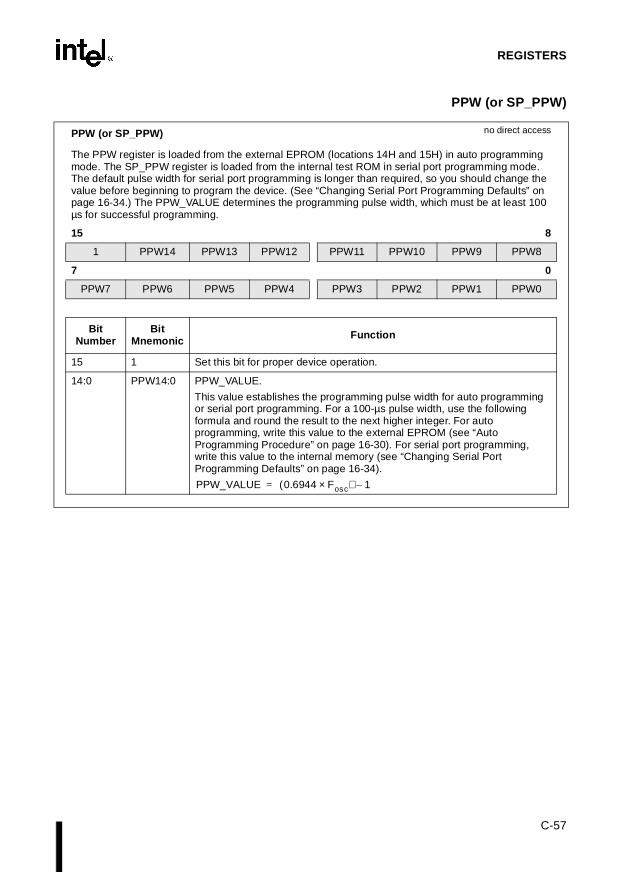
C-57
REGISTERS
PPW (or SP_PPW)
PPW (or SP_PPW) no direct access
The PPW register is loaded from the external EPROM (locations 14H and 15H) in auto programming mode. The SP_PPW register is loaded from the internal test ROM in serial port programming mode. The default pulse width for serial port programming is longer than required, so you should change the value before beginning to program the device. (See “Changing Serial Port Programming Defaults” on page 16-34.) The PPW_VALUE determines the programming pulse width, which must be at least 100 µs for successful programming.
15 8
1 PPW14 PPW13 PPW12 PPW11 PPW10 PPW9 PPW8
7 0
PPW7 PPW6 PPW5 PPW4 PPW3 PPW2 PPW1 PPW0
Bit Number
BitMnemonic Function
15 1 Set this bit for proper device operation.
14:0 PPW14:0 PPW_VALUE.
This value establishes the programming pulse width for auto programming or serial port programming. For a 100-µs pulse width, use the following formula and round the result to the next higher integer. For auto programming, write this value to the external EPROM (see “Auto Programming Procedure” on page 16-30). For serial port programming, write this value to the internal memory (see “Changing Serial Port Programming Defaults” on page 16-34).
PPW_VALUE 0.6944 Fosc×( ) 1–=

8XC196Kx, Jx, CA USER’S MANUAL
C-58
PSW
PSW no direct access
The processor status word (PSW) actually consists of two bytes. The high byte is the status word, which is described here; the low byte is the INT_MASK register. The status word contains one bit (PSW.1) that globally enables or disables servicing of all maskable interrupts, one bit (PSW.2) that enables or disables the peripheral transaction server (PTS), and six Boolean flags that reflect the state of a user’s program.
The status word portion of the PSW cannot be accessed directly. To access the status word, push the value onto the stack (PUSHF), then pop the value to a register (POP test_reg). The PUSHF and PUSHA instructions save the PSW in the system stack and then clear it; POPF and POPA restore it.
15 8
Z N V VT C PSE I ST
7 0
See INT_MASK on page C-46
Bit Number
Bit Mnemonic Function
7 Z Zero Flag
This flag is set to indicate that the result of an operation is zero. For add-with-carry and subtract-with-borrow operations, the flag is never set, but it is cleared if the result is non-zero. This way, the zero flag indicates the correct zero or non-zero result for multiple-precision calculations.
6 N Negative Flag
This flag is set to indicate that the result of an operation is negative. The flag is correct even if an overflow occurs. For all shift operations and the NORML instruction, the flag is set to equal the most-significant bit of the result, even if the shift count is zero.
5 V Overflow Flag
This flag is set to indicate that the result of an operation is too large to be represented correctly in the available space. For shift operations (SHL, SHLB, and SHLL), the flag is set if the most-significant bit of the operand changes during the shift.
4 VT Overflow-trap Flag
This flag is set when the overflow flag is set, but it is cleared only by the CLRVT, JVT, and JNVT instructions. This allows testing for a possible overflow condition at the end of a sequence of related arithmetic operations, which is generally more efficient than testing the overflow flag after each operation.
3 C Carry Flag
This flag is set to indicate an arithmetic carry or the last bit shifted out of an operand. It is cleared if a subtraction operation generates a borrow. Normally, the result is rounded up if the carry flag is set. The sticky bit flag allows a finer resolution in the rounding decision. (See the PSW flag descriptions in Appendix A for details.)
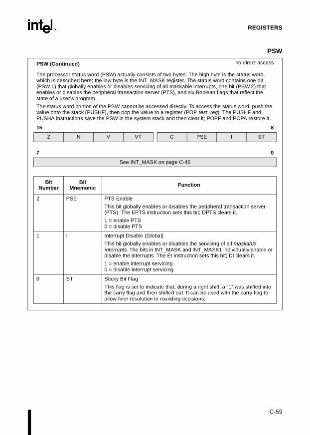
C-59
REGISTERS
PSW
2 PSE PTS Enable
This bit globally enables or disables the peripheral transaction server (PTS). The EPTS instruction sets this bit; DPTS clears it.
1 = enable PTS0 = disable PTS
1 I Interrupt Disable (Global)
This bit globally enables or disables the servicing of all maskable interrupts. The bits in INT_MASK and INT_MASK1 individually enable or disable the interrupts. The EI instruction sets this bit; DI clears it.
1 = enable interrupt servicing0 = disable interrupt servicing
0 ST Sticky Bit Flag
This flag is set to indicate that, during a right shift, a “1” was shifted into the carry flag and then shifted out. It can be used with the carry flag to allow finer resolution in rounding decisions.
PSW (Continued) no direct access
The processor status word (PSW) actually consists of two bytes. The high byte is the status word, which is described here; the low byte is the INT_MASK register. The status word contains one bit (PSW.1) that globally enables or disables servicing of all maskable interrupts, one bit (PSW.2) that enables or disables the peripheral transaction server (PTS), and six Boolean flags that reflect the state of a user’s program.
The status word portion of the PSW cannot be accessed directly. To access the status word, push the value onto the stack (PUSHF), then pop the value to a register (POP test_reg). The PUSHF and PUSHA instructions save the PSW in the system stack and then clear it; POPF and POPA restore it.
15 8
Z N V VT C PSE I ST
7 0
See INT_MASK on page C-46
Bit Number
Bit Mnemonic Function

8XC196Kx USER’S MANUAL
C-60
PTSSEL
PTSSEL Address:Reset State:
04H0000H
The PTS select (PTSSEL) register selects either a PTS microcode routine or a standard interrupt service routine for each interrupt requests. Setting a bit selects a PTS microcode routine; clearing a bit selects a standard interrupt service routine. When PTSCOUNT reaches zero, hardware clears the corresponding PTSSEL bit. The PTSSEL bit must be set manually to re-enable the PTS channel.
15 8
87C196CA — EXTINT CAN RI TI SSIO1 SSIO0 —
7 0
— — AD EPA0 EPA1 EPA2 EPA3 EPAx
15 8
8XC196Jx — EXTINT — RI TI SSIO1 SSIO0 —
7 0
— — AD EPA0 EPA1 EPA2 EPA3 EPAx
15 8
8XC196Kx — EXTINT — RI TI SSIO1 SSIO0 CBF
7 0
IBF OBE AD EPA0 EPA1 EPA2 EPA3 EPAx
BitNumber Function
14:0(Note 1)
Setting this bit causes the corresponding interrupt to be handled by a PTS microcode routine.
The PTS interrupt vector locations are as follows:
Bit Mnemonic Interrupt PTS VectorEXTINT EXTINT pin 205CHCAN (CA)† CAN Peripheral 205AHRI SIO Receive 2058HTI SIO Transmit 2056HSSIO1 SSIO 1 Transfer 2054HSSIO0 SSIO 0 Transfer 2052HCBF (Kx) Slave Port Command Buffer Full 2050HIBF (Kx) Slave Port Input Buffer Full 204EHOBE (Kx) Slave Port Output Buffer Empty 204CHAD A/D Conversion Complete 204AHEPA0 EPA Capture/Compare Channel 0 2048HEPA1 EPA Capture/Compare Channel 1 2046HEPA2 EPA Capture/Compare Channel 2 2044HEPA3 EPA Capture/Compare Channel 3 2042HEPAx† Multiplexed EPA 2040H
† PTS service is not recommended because the PTS cannot determine the source of multiplexed interrupts.
1. Bit 13 is reserved on the 8XC196Jx, Kx devices and bits 6–8 are reserved on the 87C196CA,8XC196Jx devices. For compatibility with future devices, write zeros to these bits.
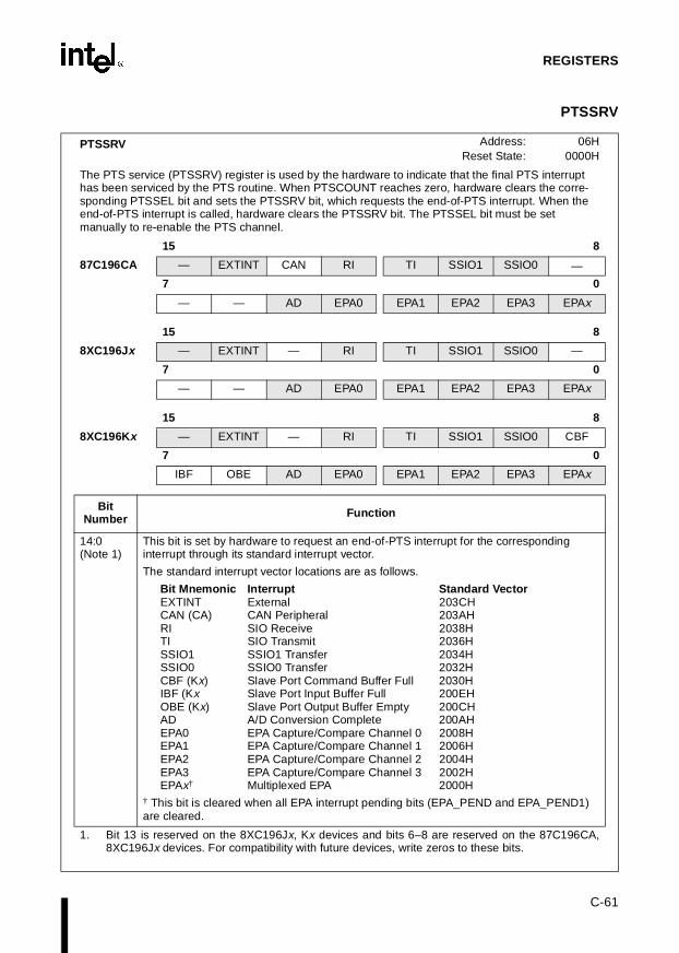
C-61
REGISTERS
PTSSRV
PTSSRV Address:Reset State:
06H0000H
The PTS service (PTSSRV) register is used by the hardware to indicate that the final PTS interrupt has been serviced by the PTS routine. When PTSCOUNT reaches zero, hardware clears the corre-sponding PTSSEL bit and sets the PTSSRV bit, which requests the end-of-PTS interrupt. When the end-of-PTS interrupt is called, hardware clears the PTSSRV bit. The PTSSEL bit must be set manually to re-enable the PTS channel.
15 8
87C196CA — EXTINT CAN RI TI SSIO1 SSIO0 —
7 0
— — AD EPA0 EPA1 EPA2 EPA3 EPAx
15 8
8XC196Jx — EXTINT — RI TI SSIO1 SSIO0 —
7 0
— — AD EPA0 EPA1 EPA2 EPA3 EPAx
15 8
8XC196Kx — EXTINT — RI TI SSIO1 SSIO0 CBF
7 0
IBF OBE AD EPA0 EPA1 EPA2 EPA3 EPAx
BitNumber Function
14:0(Note 1)
This bit is set by hardware to request an end-of-PTS interrupt for the corresponding interrupt through its standard interrupt vector.
The standard interrupt vector locations are as follows.
Bit Mnemonic Interrupt Standard VectorEXTINT External 203CHCAN (CA) CAN Peripheral 203AHRI SIO Receive 2038HTI SIO Transmit 2036HSSIO1 SSIO1 Transfer 2034HSSIO0 SSIO0 Transfer 2032HCBF (Kx) Slave Port Command Buffer Full 2030HIBF (Kx Slave Port Input Buffer Full 200EHOBE (Kx) Slave Port Output Buffer Empty 200CHAD A/D Conversion Complete 200AHEPA0 EPA Capture/Compare Channel 0 2008HEPA1 EPA Capture/Compare Channel 1 2006HEPA2 EPA Capture/Compare Channel 2 2004HEPA3 EPA Capture/Compare Channel 3 2002HEPAx† Multiplexed EPA 2000H
† This bit is cleared when all EPA interrupt pending bits (EPA_PEND and EPA_PEND1) are cleared.
1. Bit 13 is reserved on the 8XC196Jx, Kx devices and bits 6–8 are reserved on the 87C196CA,8XC196Jx devices. For compatibility with future devices, write zeros to these bits.

8XC196Kx, Jx, CA USER’S MANUAL
C-62
SBUF_RX
SBUF_RX Address:Reset State:
1FB8H00H
The serial port receive buffer (SBUF_RX) register contains data received from the serial port. The serial port receiver is buffered and can begin receiving a second data byte before the first byte is read. Data is held in the receive shift register until the last data bit is received, then the data byte is loaded into SBUF_RX. If data in the shift register is loaded into SBUF_RX before the previous byte is read, the overflow error bit is set (SP_STATUS.2). The data in SBUF_RX will always be the last byte received, never a combination of the last two bytes.
7 0
Data Received
Bit Number Function
7:0 Data Received
This register contains the last byte of data received from the serial port.
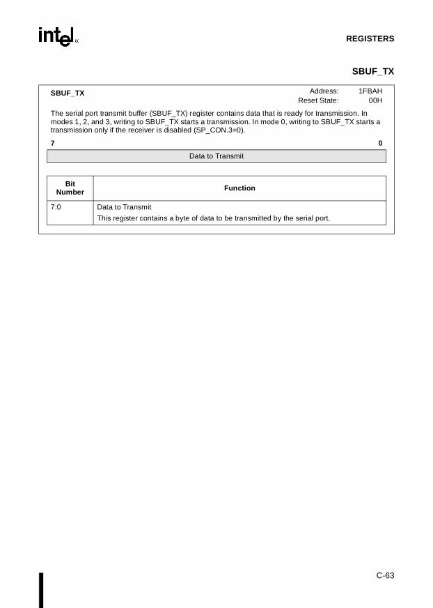
C-63
REGISTERS
SBUF_TX
SBUF_TX Address:Reset State:
1FBAH00H
The serial port transmit buffer (SBUF_TX) register contains data that is ready for transmission. In modes 1, 2, and 3, writing to SBUF_TX starts a transmission. In mode 0, writing to SBUF_TX starts a transmission only if the receiver is disabled (SP_CON.3=0).
7 0
Data to Transmit
Bit Number Function
7:0 Data to Transmit
This register contains a byte of data to be transmitted by the serial port.

8XC196Kx, Jx, CA USER’S MANUAL
C-64
SLP_CMD
SLP_CMD(8XC196Kx)
Address:Reset State:
1FFAH00H
The slave port comand (SLP_CMD) register accepts commands from the master to the slave. The commands are defined by the device software. The slave can read from and write to this register. The master can only write to it. To write to SLP_CMD (rather than P3_PIN) the master must first write “1” to the pin selected by SLP_CON.2.
7 0
8XC196Kx Command Value
Bit Number Function
7:0 Command Value
This register is used to hold commands from the master to the slave.

C-65
REGISTERS
SLP_CON
SLP_CON(8XC196Kx)
Address:Reset State:
1FFBH00H
The slave port control (SLP_CON) register is used to configure the slave port. Only the slave can access the register.
7 0
KQ, KR — — — — SLP SLPL IBEMSK OBFMSK
7 0
KS, KT — — — SME SLP SLPL IBEMSK OBFMSK
BitNumber
BitMnemonic Function
7:5 — Reserved; always write as zeros.
4† SME Shared Memory Enable
Enables slave port shared memory mode.
1 = shared memory mode0 = standard slave mode
3 SLP Slave Port Enable
This bit enables or disables the slave port.
1 = enables the slave port0 = disables the slave port and clears the command buffer empty (CBE),
input buffer empty (IBE), and output buffer full (OBF) flags in the SLP_STAT register.
2 SLPL Slave Port Latch
In standard slave mode only, this bit determines the source of the internal control signal, SLP_ADDR. When SLP_ADDR is held high, the master can write to the SLP_CMD register and read from the SLP_STAT register. When SLP_ADDR is held low, the master can write to the P3_PIN register and read from the P3_REG register.
1 = SLP1 (P3.1) via master’s AD1 signal. Use with multiplexed bus.0 = SLPALE (P5.0) via master’s A1 signal. Use with demultiplexed bus.
In shared memory mode, this bit has no function.
1 IBEMSK Input Buffer Empty Mask
Controls whether the IBE flag (in SLP_STAT) asserts the SLPINT signal.
In shared memory mode, this bit has no effect on the SLPINT signal.
0 OBFMSK Output Buffer Full Mask
Controls whether the OBF flag (in SLP_STAT) asserts the SLPINT signal.
In shared memory mode, this bit has no effect on the SLPINT signal.
† On the 8XC196KQ, KR devices this bit is reserved; always write as zero.

8XC196Kx, Jx, CA USER’S MANUAL
C-66
SLP_STAT
SLP_STAT(8XC196Kx)
Address:Reset State:
1FF8H00H
The master can read the slave port status (SLP_STAT) register to determine the status of the slave. The slave can read all bits and can write bits 3–7 for general-purpose status information. (The bits are user-defined flags.) If the master attempts to write to SLP_STAT, it actually writes to SLP_CMD. To read from this register (rather than P3_REG), the master must first write “1” to the pin selected by SLP_CON.2.
7 0
KQ, KR SF4 SF3 SF2 SF1 SF0 CBE IBE OBF
7 0
KS, KT SMO/SF4 SF3 SF2 SF1 SF0 CBE IBE OBF
BitNumber
BitMnemonic Function
7† (KS, KT) SMO/SF4 Shared Memory Operation/Status Field Bit 4
In shared memory mode bit 7 (SMO) indicates whether the bus interface logic received a read (1) or a write (0). SMO can be read but not written.
In standard slave mode bit 7 (SF4) is the high bit of the status field.
7:3 (KQ, KR)6:3 (KS, KT)
SF4:0SF3:0
Status Field
The slave can write to these bits for general-purpose status infor-mation. (The bits are user-defined flags).
2 CBE Command Buffer Empty
This flag is set after the slave reads SLP_CMD. The flag is cleared and the command buffer full (CBF) interrupt pending bit (INT_PEND1.0) is set after the master writes to SLP_CMD.
1 IBE Input Buffer Empty
This flag is set after the slave reads P3_PIN. The flag is cleared and the IBF interrupt pending bit (INT_PEND.7) is set after the master writes to P3_PIN.
0 OBF Output Buffer Full
This flag is set after the slave writes to P3_REG. The flag is cleared and the OBE interrupt pending bit (INT_PEND.6) is set after the master reads P3_REG.
† On the 8XC196KQ, KR devices this bit functions only as SF4.

C-67
REGISTERS
SP
SP Address:Reset State:
18HXXXXH
The system’s stack pointer (SP) can point anywhere in internal or external memory; it must be word aligned and must always be initialized before use. The stack pointer is decremented before a PUSH and incremented after a POP, so the stack pointer should be initialized to two bytes above the highest stack location. If stack operations are not being performed, locations 18H and 19H may be used as standard registers.
15 8
Stack Pointer (high byte)
7 0
Stack Pointer (low byte)
Bit Number Function
15:0 Stack Pointer
This register makes up the system’s stack pointer.

8XC196Kx, Jx, CA USER’S MANUAL
C-68
SP_BAUD
SP_BAUD Address:Reset State:
1FBCH0000H
The serial port baud rate (SP_BAUD) register selects the serial port baud rate and clock source. The most-significant bit selects the clock source. The lower 15 bits represent BAUD_VALUE, an unsigned integer that determines the baud rate.
The maximum BAUD_VALUE is 32,767 (7FFFH). In asynchronous modes 1, 2, and 3, the minimum BAUD_VALUE is 0000H when using XTAL1 and 0001H when using T1CLK. In synchronous mode 0, the minimum BAUD_VALUE is 0001H for transmissions and 0002H for receptions.
15 8
CA, Jx — BV14 BV13 BV12 BV11 BV10 BV9 BV8
7 0
BV7 BV6 BV5 BV4 BV3 BV2 BV1 BV0
15 8
Kx CLKSRC BV14 BV13 BV12 BV11 BV10 BV9 BV8
7 0
BV7 BV6 BV5 BV4 BV3 BV2 BV1 BV0
BitNumber
BitMnemonic Function
15† CLKSRC Serial Port Clock Source
This bit determines whether the serial port is clocked from an internal or an external source.
1 = XTAL1 (internal source)0 = T1CLK (external source)
14:0 BV14:0 These bits constitute the BAUD_VALUE.
Use the following equations to determine the BAUD_VALUE for a given baud rate.
Synchronous mode 0:††
or
Asynchronous modes 1, 2, and 3:
or
†† For mode 0 receptions, the BAUD_VALUE must be 0002H or greater. Otherwise, the resulting data in the receive shift register will be incorrect.
† On the 87C196CA, 8XC196Jx devices the T1CLK pin is not implemented; therefore, on these devices this bit is reserved and should be written as one.
BAUD_VALUEFOSC
Baud Rate 2×-------------------------------------- 1–=
T1CLK
Baud Rate----------------------------
BAUD_VALUEFOSC
Baud Rate 16×----------------------------------------- 1–=
T1CLK
Baud Rate 8×--------------------------------------
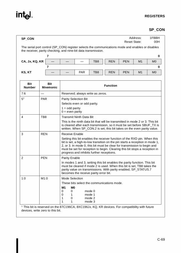
C-69
REGISTERS
SP_CON
SP_CON Address:Reset State:
1FBBH00H
The serial port control (SP_CON) register selects the communications mode and enables or disables the receiver, parity checking, and nine-bit data transmission.
7 0
CA, Jx, KQ, KR — — — TB8 REN PEN M1 M0
7 0
KS, KT — — PAR TB8 REN PEN M1 M0
BitNumber
BitMnemonic Function
7:6 — Reserved; always write as zeros.
5† PAR Parity Selection Bit
Selects even or odd parity.
1 = odd parity0 = even parity
4 TB8 Transmit Ninth Data Bit
This is the ninth data bit that will be transmitted in mode 2 or 3. This bit is cleared after each transmission, so it must be set before SBUF_TX is written. When SP_CON.2 is set, this bit takes on the even parity value.
3 REN Receive Enable
Setting this bit enables the receiver function of the RXD pin. When this bit is set, a high-to-low transition on the pin starts a reception in mode 1, 2, or 3. In mode 0, this bit must be clear for transmission to begin and must be set for reception to begin. Clearing this bit stops a reception in progress and inhibits further receptions.
2 PEN Parity Enable
In modes 1 and 3, setting this bit enables the parity function. This bit must be cleared if mode 2 is used. When this bit is set, TB8 takes the parity value on transmissions. With parity enabled, SP_STATUS.7 becomes the receive parity error bit.
1:0 M1:0 Mode Selection
These bits select the communications mode.
M1 M00 0 mode 00 1 mode 11 0 mode 21 1 mode 3
† This bit is reserved on the 87C196CA, 8XC196Jx, KQ, KR devices. For compatibility with future devices, write zero to this bit.
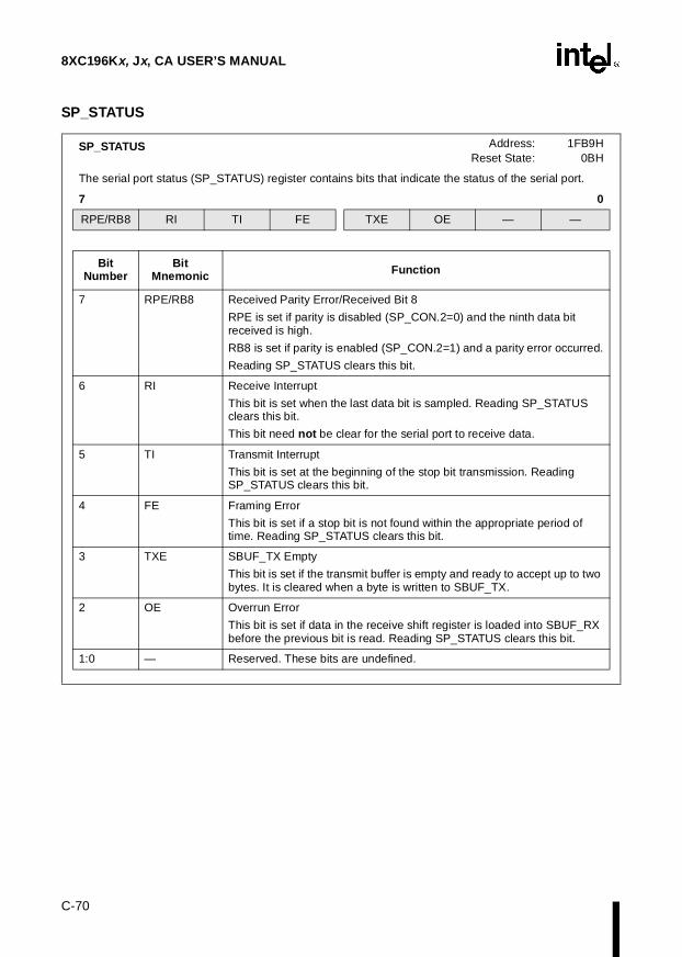
8XC196Kx, Jx, CA USER’S MANUAL
C-70
SP_STATUS
SP_STATUS Address:Reset State:
1FB9H0BH
The serial port status (SP_STATUS) register contains bits that indicate the status of the serial port.
7 0
RPE/RB8 RI TI FE TXE OE — —
Bit Number
Bit Mnemonic Function
7 RPE/RB8 Received Parity Error/Received Bit 8
RPE is set if parity is disabled (SP_CON.2=0) and the ninth data bit received is high.
RB8 is set if parity is enabled (SP_CON.2=1) and a parity error occurred.
Reading SP_STATUS clears this bit.
6 RI Receive Interrupt
This bit is set when the last data bit is sampled. Reading SP_STATUS clears this bit.
This bit need not be clear for the serial port to receive data.
5 TI Transmit Interrupt
This bit is set at the beginning of the stop bit transmission. Reading SP_STATUS clears this bit.
4 FE Framing Error
This bit is set if a stop bit is not found within the appropriate period of time. Reading SP_STATUS clears this bit.
3 TXE SBUF_TX Empty
This bit is set if the transmit buffer is empty and ready to accept up to two bytes. It is cleared when a byte is written to SBUF_TX.
2 OE Overrun Error
This bit is set if data in the receive shift register is loaded into SBUF_RX before the previous bit is read. Reading SP_STATUS clears this bit.
1:0 — Reserved. These bits are undefined.

C-71
REGISTERS
SSIO_BAUD
SSIO_BAUD Address:Reset State:
1FB4HXXH
The synchronous serial port baud (SSIO_BAUD) register enables and disables the baud-rate generator and selects the SSIO baud rate. During read operations, SSIO_BAUD serves as the down-counter monitor. The down-counter is decremented once every four state times when the baud-rate generator is enabled.
7 0
BE BV6 BV5 BV4 BV3 BV2 BV1 BV0
Bit Number
Bit Mnemonic Function
7 BE Baud-rate Generator Enable
This bit enables and disables the baud-rate generator.
For write operations:
0 = disable the baud-rate generator and clear BV6:01 = enable the baud-rate generator and start the down-counter
For read operations:
0 = baud-rate generator is disabled1 = baud-rate generator is enabled and down-counter is running
6:0 BV6:0 Baud Value
For write operations:
These bits represent BAUD_VALUE, an unsigned integer that determines the baud rate. The maximum value of BAUD_VALUE is 7FH; the minimum value is 0. Use the following equation to determine BAUD_VALUE for a given baud rate.
For read operations:
These bits contain the current value of the down-counter.
Table C-20. Common SSIO_BAUD Values at 16 MHz
Baud Rate SSIO_BAUD Value †
(Maximum) 2.0 MHz 80H
100.0 kHz 93H
64.52 kHz 9DH
50.0 kHz A7H
25.0 kHz CFH
(Minimum) 15.625 kHz FFH
† Bit 7 must be set to enable the baud-rate generator.
BAUD_VALUEFOSC
Baud Rate 8×-------------------------------------- 1–=

8XC196Kx, Jx, CA USER’S MANUAL
C-72
SSIOx_BUF (RXD, TXD)
SSIOx_BUF (RXD, TXD)x = 0–1
Address:Reset State:
Table C-21
The synchronous serial receive buffer x (SSIOx_BUF (RXD)) contains received data. Data is shifted into this register from the SDx pin, with the most-significant bit first.
The synchronous serial transmit buffer x (SSIOx_BUF (TXD)) contains data for transmission. Data is shifted from this register to the SDx pin, with the most-significant bit first.
7 0
RXD Data Received
7 0
TXD Data to Transmit
BitNumber Function
7:0 Data Received
During receptions, this register contains the last byte of data received from the synchronous serial port.
Data to Transmit
During transmissions, this register contains a byte of data to be transmitted by the synchronous serial port.
Table C-21. SSIOx_BUF Addresses and Reset Values
Register Address Reset Value
SSIO0_BUF 1FB0H 00H
SSIO1_BUF 1FB2H 00H
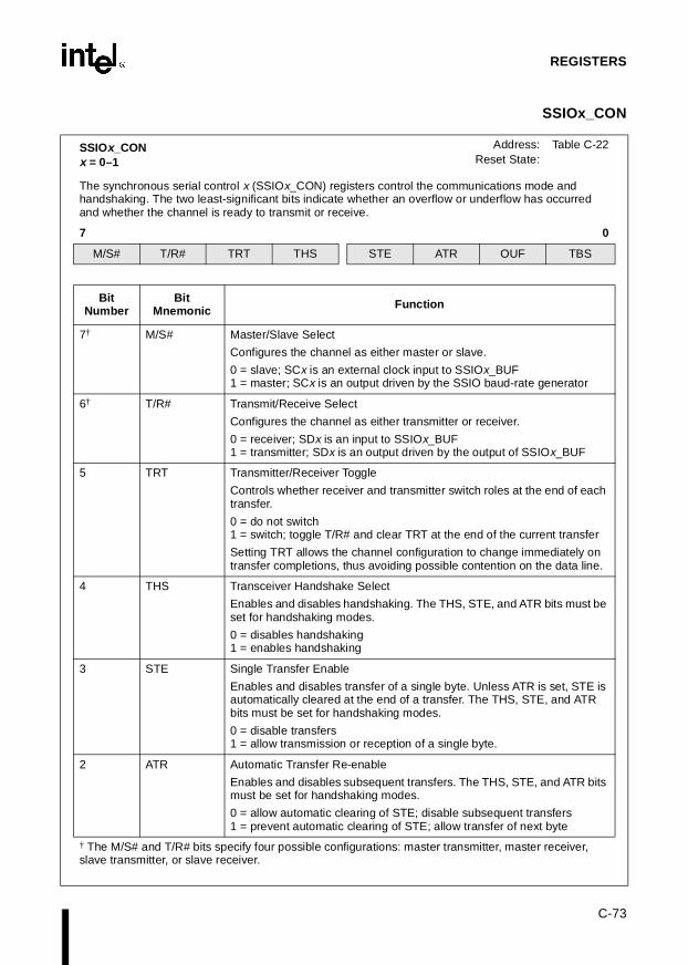
C-73
REGISTERS
SSIOx_CON
SSIOx_CON x = 0–1
Address:Reset State:
Table C-22
The synchronous serial control x (SSIOx_CON) registers control the communications mode and handshaking. The two least-significant bits indicate whether an overflow or underflow has occurred and whether the channel is ready to transmit or receive.
7 0
M/S# T/R# TRT THS STE ATR OUF TBS
Bit Number
Bit Mnemonic Function
7† M/S# Master/Slave Select
Configures the channel as either master or slave.
0 = slave; SCx is an external clock input to SSIOx_BUF1 = master; SCx is an output driven by the SSIO baud-rate generator
6† T/R# Transmit/Receive Select
Configures the channel as either transmitter or receiver.
0 = receiver; SDx is an input to SSIOx_BUF1 = transmitter; SDx is an output driven by the output of SSIOx_BUF
5 TRT Transmitter/Receiver Toggle
Controls whether receiver and transmitter switch roles at the end of each transfer.
0 = do not switch1 = switch; toggle T/R# and clear TRT at the end of the current transfer
Setting TRT allows the channel configuration to change immediately on transfer completions, thus avoiding possible contention on the data line.
4 THS Transceiver Handshake Select
Enables and disables handshaking. The THS, STE, and ATR bits must be set for handshaking modes.
0 = disables handshaking1 = enables handshaking
3 STE Single Transfer Enable
Enables and disables transfer of a single byte. Unless ATR is set, STE is automatically cleared at the end of a transfer. The THS, STE, and ATR bits must be set for handshaking modes.
0 = disable transfers1 = allow transmission or reception of a single byte.
2 ATR Automatic Transfer Re-enable
Enables and disables subsequent transfers. The THS, STE, and ATR bits must be set for handshaking modes.
0 = allow automatic clearing of STE; disable subsequent transfers1 = prevent automatic clearing of STE; allow transfer of next byte
† The M/S# and T/R# bits specify four possible configurations: master transmitter, master receiver, slave transmitter, or slave receiver.
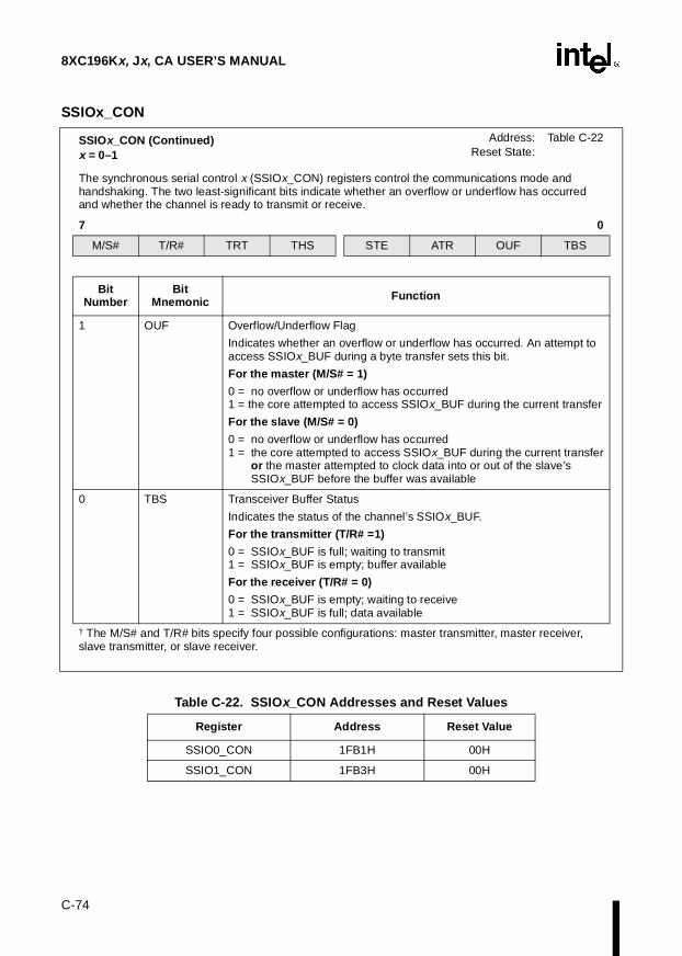
8XC196Kx, Jx, CA USER’S MANUAL
C-74
SSIOx_CON
1 OUF Overflow/Underflow Flag
Indicates whether an overflow or underflow has occurred. An attempt to access SSIOx_BUF during a byte transfer sets this bit.
For the master (M/S# = 1)
0 = no overflow or underflow has occurred1 = the core attempted to access SSIOx_BUF during the current transfer
For the slave (M/S# = 0)
0 = no overflow or underflow has occurred1 = the core attempted to access SSIOx_BUF during the current transfer
or the master attempted to clock data into or out of the slave’s SSIOx_BUF before the buffer was available
0 TBS Transceiver Buffer Status
Indicates the status of the channel’s SSIOx_BUF.
For the transmitter (T/R# =1)
0 = SSIOx_BUF is full; waiting to transmit1 = SSIOx_BUF is empty; buffer available
For the receiver (T/R# = 0)
0 = SSIOx_BUF is empty; waiting to receive1 = SSIOx_BUF is full; data available
Table C-22. SSIOx_CON Addresses and Reset Values
Register Address Reset Value
SSIO0_CON 1FB1H 00H
SSIO1_CON 1FB3H 00H
SSIOx_CON (Continued)x = 0–1
Address:Reset State:
Table C-22
The synchronous serial control x (SSIOx_CON) registers control the communications mode and handshaking. The two least-significant bits indicate whether an overflow or underflow has occurred and whether the channel is ready to transmit or receive.
7 0
M/S# T/R# TRT THS STE ATR OUF TBS
Bit Number
Bit Mnemonic Function
† The M/S# and T/R# bits specify four possible configurations: master transmitter, master receiver, slave transmitter, or slave receiver.

C-75
REGISTERS
T1CONTROL
T1CONTROL Address:Reset State:
1F98H00H
The timer 1 control (T1CONTROL) register determines the clock source, counting direction, and count rate for timer 1.
7 0
CE UD M2 M1 M0 P2 P1 P0
Bit Number
Bit Mnemonic Function
7 CE Counter Enable
This bit enables or disables the timer. From reset, the timers are disabled and not free running.
0 = disables timer1 = enables timer
6 UD Up/Down
This bit determines the timer counting direction, in selected modes (see mode bits, M2:0)
0 = count down1 = count up
5:3 M2:0 EPA Clock Direction Mode Bits
These bits determine the timer clocking source and direction control source.
M2 M1 M0 Clock Source Direction Source
0 0 0 FOSC/4 UD bit (T1CONTROL.6)X 0 1 T1CLK Pin† UD bit (T1CONTROL.6)††
0 1 0 FOSC/4 T1DIR Pin††
0 1 1 T1CLK Pin† T1DIR Pin††
1 1 1 quadrature clocking using T1CLK and T1DIR pins††
† If an external clock is selected, the timer counts on both the rising and falling edges of the clock.†† These modes are reserved on the 8XC196CA, Jx devices.
2:0 P2:0 EPA Clock Prescaler Bits
These bits determine the clock prescaler value.
P2 P1 P0 Prescaler Resolution (at 16 MHz)
0 0 0 divide by 1 (disabled) 250 ns0 0 1 divide by 2 500 ns0 1 0 divide by 4 1 µs0 1 1 divide by 8 2 µs1 0 0 divide by 16 4 µs1 0 1 divide by 32 8 µs1 1 0 divide by 64 16 µs1 1 1 reserved —

8XC196Kx, Jx, CA USER’S MANUAL
C-76
T2CONTROL
T2CONTROL Address:Reset State:
1F9CH00H
The timer 2 control (T2CONTROL) register determines the clock source, counting direction, and count rate for timer 2.
7 0
CE UD M2 M1 M0 P2 P1 P0
Bit Number
Bit Mnemonic Function
7 CE Counter Enable
This bit enables or disables the timer. From reset, the timers are disabled and not free running.
0 = disables timer1 = enables timer
6 UD Up/Down
This bit determines the timer counting direction, in selected modes (see mode bits, M2:0).
0 = count down1 = count up
5:3 M2:0 EPA Clock Direction Mode Bits.
These bits determine the timer clocking source and direction source
M2 M1 M0 Clock Source Direction Source
0 0 0 FOSC/4 UD bit (T2CONTROL.6)X 0 1 T2CLK Pin† UD bit (T2CONTROL.6)0 1 0 FOSC/4 T2DIR Pin0 1 1 T2CLK Pin† T2DIR Pin1 0 0 timer 1 overflow UD bit (T2CONTROL.6)1 1 0 timer 1 same as timer 11 1 1 quadrature clocking using T2CLK and T2DIR pins† If an external clock is selected, the timer counts on both the rising and falling edges of the clock.
2:0 P2:0 EPA Clock Prescaler Bits
These bits determine the clock prescaler value.
P2 P1 P0 Prescaler Resolution (at 16 MHz)
0 0 0 divide by 1 (disabled) 250 ns0 0 1 divide by 2 500 ns0 1 0 divide by 4 1 µs0 1 1 divide by 8 2 µs1 0 0 divide by 16 4 µs1 0 1 divide by 32 8 µs1 1 0 divide by 64 16 µs1 1 1 reserved —

C-77
REGISTERS
TIMERx
TIMERxx = 1–2
Address:Reset State:
Table C-23
The two bytes of the timer x register contain the value of timer x. This register can be written, allowing timer x to be initialized to a value other than zero.
15 8
Timer Value (high byte)
7 0
Timer Value (low byte)
Bit Number Function
15:0 Timer
Read the current timer x value from this register or write a new timer x value to this register.
Table C-23. TIMERx Addresses and Reset Values
Register Address Reset Value
TIMER1 1F9AH 0000H
TIMER2 1F9EH 0000H
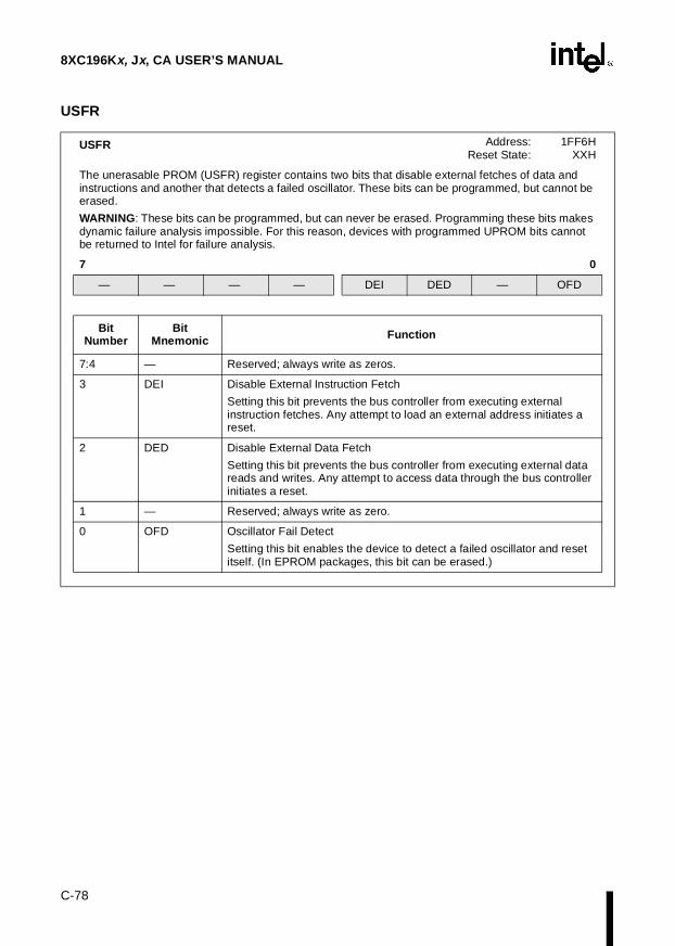
8XC196Kx, Jx, CA USER’S MANUAL
C-78
USFR
USFR Address:Reset State:
1FF6HXXH
The unerasable PROM (USFR) register contains two bits that disable external fetches of data and instructions and another that detects a failed oscillator. These bits can be programmed, but cannot be erased.
WARNING: These bits can be programmed, but can never be erased. Programming these bits makes dynamic failure analysis impossible. For this reason, devices with programmed UPROM bits cannot be returned to Intel for failure analysis.
7 0
— — — — DEI DED — OFD
Bit Number
Bit Mnemonic Function
7:4 — Reserved; always write as zeros.
3 DEI Disable External Instruction Fetch
Setting this bit prevents the bus controller from executing external instruction fetches. Any attempt to load an external address initiates a reset.
2 DED Disable External Data Fetch
Setting this bit prevents the bus controller from executing external data reads and writes. Any attempt to access data through the bus controller initiates a reset.
1 — Reserved; always write as zero.
0 OFD Oscillator Fail Detect
Setting this bit enables the device to detect a failed oscillator and reset itself. (In EPROM packages, this bit can be erased.)

C-79
REGISTERS
WATCHDOG
WATCHDOG Address:Reset State:
0AH00H
Unless it is cleared every 64K state times, the watchdog timer resets the device. To clear the watchdog timer, send “1EH” followed immediately by “E1H” to location 0AH. Clearing this register the first time enables the watchdog with an initial value of 0000H, which is incremented once every state time. After it is enabled, the watchdog can be disabled only by a reset.
The WDE bit (bit 3) of CCR1 controls whether the watchdog is enabled immediately or is disabled until the first time it is cleared. Clearing WDE activates the watchdog. Setting WDE makes the watchdog timer inactive, but you can activate it by clearing the watchdog register. Once the watchdog is activated, only a reset can disable it.
7 0
Watchdog Timer Value
Bit Number Function
7:0 Watchdog Timer Value
This register contains the 8 most-significant bits of the current value of the watchdog timer.

8XC196Kx, Jx, CA USER’S MANUAL
C-80
WSR
WSR Address:Reset State:
14H00H
The window selection register (WSR) has two functions. One bit enables and disables the bus-hold protocol. The remaining bits select windows. Windows map sections of RAM into the upper section of the lower register file, in 32-, 64-, or 128-byte increments. PUSHA saves this register on the stack and POPA restores it.
7 0
CA, Jx — W6 W5 W4 W3 W2 W1 W0
7 0
Kx HLDEN W6 W5 W4 W3 W2 W1 W0
BitNumber
BitMnemonic Function
7† HLDEN Hold Enable:
This bit enables and disables the bus-hold protocol (see Chapter 15, “Enabling the Bus-hold Protocol (8XC196Kx Only)”). It has no effect on windowing.
1 = bus-hold protocol enabled0 = bus-hold protocol disabled
6:0 W6:0 Window Selection:
These bits specify the window size and window number:
6 5 4 3 2 1 0
1 x x x x x x 32-byte window; W5:0 = window number
0 1 x x x x x 64-byte window; W4:0 = window number
0 0 1 x x x x 128-byte window; W3:0 = window number
† On the 87C196CA, 8XC196Jx devices this bit is reserved; always write as zero.
Table C-24. WSR Settings and Direct Addresses for Windowable SFRs
Register Mnemonic MemoryLocation
32-Byte Windows(00E0–00FFH)
64-Byte Windows(00C0–00FFH)
128-Byte Windows(0080–00FFH)
WSR Direct Address WSR Direct
Address WSR Direct Address
AD_COMMAND 1FACH 7DH 00ECH 3EH 00ECH 1FH 00ACH
AD_RESULT 1FAAH 7DH 00EAH 3EH 00EAH 1FH 00AAH
AD_TEST 1FAEH 7DH 00EEH 3EH 00EEH 1FH 00AEH
AD_TIME 1FAFH 7DH 00EFH 3EH 00EFH 1FH 00AFH
CAN_BTIME0 (CA) 1E3FH 71H 00FFH 38H 00FFH 1CH 00BFH
CAN_BTIME1 (CA) 1E4FH 72H 00EFH 39H 00CFH 1CH 00CFH
† Must be addressed as a word.
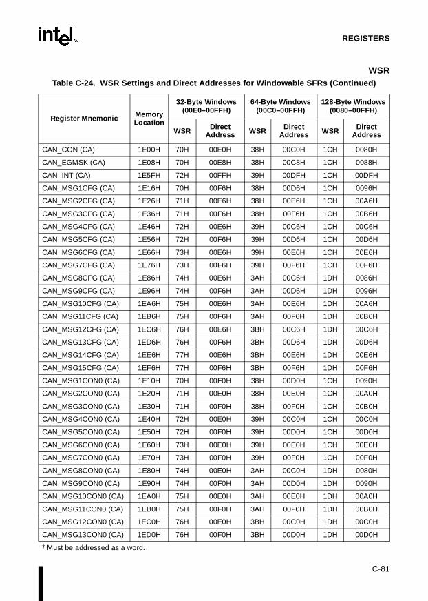
C-81
REGISTERS
WSR
CAN_CON (CA) 1E00H 70H 00E0H 38H 00C0H 1CH 0080H
CAN_EGMSK (CA) 1E08H 70H 00E8H 38H 00C8H 1CH 0088H
CAN_INT (CA) 1E5FH 72H 00FFH 39H 00DFH 1CH 00DFH
CAN_MSG1CFG (CA) 1E16H 70H 00F6H 38H 00D6H 1CH 0096H
CAN_MSG2CFG (CA) 1E26H 71H 00E6H 38H 00E6H 1CH 00A6H
CAN_MSG3CFG (CA) 1E36H 71H 00F6H 38H 00F6H 1CH 00B6H
CAN_MSG4CFG (CA) 1E46H 72H 00E6H 39H 00C6H 1CH 00C6H
CAN_MSG5CFG (CA) 1E56H 72H 00F6H 39H 00D6H 1CH 00D6H
CAN_MSG6CFG (CA) 1E66H 73H 00E6H 39H 00E6H 1CH 00E6H
CAN_MSG7CFG (CA) 1E76H 73H 00F6H 39H 00F6H 1CH 00F6H
CAN_MSG8CFG (CA) 1E86H 74H 00E6H 3AH 00C6H 1DH 0086H
CAN_MSG9CFG (CA) 1E96H 74H 00F6H 3AH 00D6H 1DH 0096H
CAN_MSG10CFG (CA) 1EA6H 75H 00E6H 3AH 00E6H 1DH 00A6H
CAN_MSG11CFG (CA) 1EB6H 75H 00F6H 3AH 00F6H 1DH 00B6H
CAN_MSG12CFG (CA) 1EC6H 76H 00E6H 3BH 00C6H 1DH 00C6H
CAN_MSG13CFG (CA) 1ED6H 76H 00F6H 3BH 00D6H 1DH 00D6H
CAN_MSG14CFG (CA) 1EE6H 77H 00E6H 3BH 00E6H 1DH 00E6H
CAN_MSG15CFG (CA) 1EF6H 77H 00F6H 3BH 00F6H 1DH 00F6H
CAN_MSG1CON0 (CA) 1E10H 70H 00F0H 38H 00D0H 1CH 0090H
CAN_MSG2CON0 (CA) 1E20H 71H 00E0H 38H 00E0H 1CH 00A0H
CAN_MSG3CON0 (CA) 1E30H 71H 00F0H 38H 00F0H 1CH 00B0H
CAN_MSG4CON0 (CA) 1E40H 72H 00E0H 39H 00C0H 1CH 00C0H
CAN_MSG5CON0 (CA) 1E50H 72H 00F0H 39H 00D0H 1CH 00D0H
CAN_MSG6CON0 (CA) 1E60H 73H 00E0H 39H 00E0H 1CH 00E0H
CAN_MSG7CON0 (CA) 1E70H 73H 00F0H 39H 00F0H 1CH 00F0H
CAN_MSG8CON0 (CA) 1E80H 74H 00E0H 3AH 00C0H 1DH 0080H
CAN_MSG9CON0 (CA) 1E90H 74H 00F0H 3AH 00D0H 1DH 0090H
CAN_MSG10CON0 (CA) 1EA0H 75H 00E0H 3AH 00E0H 1DH 00A0H
CAN_MSG11CON0 (CA) 1EB0H 75H 00F0H 3AH 00F0H 1DH 00B0H
CAN_MSG12CON0 (CA) 1EC0H 76H 00E0H 3BH 00C0H 1DH 00C0H
CAN_MSG13CON0 (CA) 1ED0H 76H 00F0H 3BH 00D0H 1DH 00D0H
Table C-24. WSR Settings and Direct Addresses for Windowable SFRs (Continued)
Register Mnemonic MemoryLocation
32-Byte Windows(00E0–00FFH)
64-Byte Windows(00C0–00FFH)
128-Byte Windows(0080–00FFH)
WSR Direct Address WSR Direct
Address WSR Direct Address
† Must be addressed as a word.

8XC196Kx, Jx, CA USER’S MANUAL
C-82
WSR
CAN_MSG14CON0 (CA) 1EE0H 77H 00E0H 3BH 00E0H 1DH 00E0H
CAN_MSG15CON0 (CA) 1EF0H 77H 00F0H 3BH 00F0H 1DH 00F0H
CAN_MSG1CON1 (CA) 1E11H 70H 00F1H 38H 00D1H 1CH 0091H
CAN_MSG2CON1 (CA) 1E21H 71H 00E1H 38H 00E1H 1CH 00A1H
CAN_MSG3CON1 (CA) 1E31H 71H 00F1H 38H 00F1H 1CH 00B1H
CAN_MSG4CON1 (CA) 1E41H 72H 00E1H 39H 00C1H 1CH 00C1H
CAN_MSG5CON1 (CA) 1E51H 72H 00F1H 39H 00D1H 1CH 00D1H
CAN_MSG6CON1 (CA) 1E61H 73H 00E1H 39H 00E1H 1CH 00E1H
CAN_MSG7CON1 (CA) 1E71H 73H 00F1H 39H 00F1H 1CH 00F1H
CAN_MSG8CON1 (CA) 1E81H 74H 00E1H 3AH 00C1H 1DH 0081H
CAN_MSG9CON1 (CA) 1E91H 74H 00F1H 3AH 00D1H 1DH 0091H
CAN_MSG10CON1 (CA) 1EA1H 75H 00E1H 3AH 00E1H 1DH 00A1H
CAN_MSG11CON1 (CA) 1EB1H 75H 00F1H 3AH 00F1H 1DH 00B1H
CAN_MSG12CON1 (CA) 1EC1H 76H 00E1H 3BH 00C1H 1DH 00C1H
CAN_MSG13CON1 (CA) 1ED1H 76H 00F1H 3BH 00D1H 1DH 00D1H
CAN_MSG14CON1 (CA) 1EE1H 77H 00E1H 3BH 00E1H 1DH 00E1H
CAN_MSG15CON1 (CA) 1EF1H 77H 00F1H 3BH 00F1H 1DH 00F1H
CAN_MSG1DATA0 (CA) 1E17H 70H 00F7H 38H 00D7H 1CH 0097H
CAN_MSG2DATA0 (CA) 1E27H 71H 00E7H 38H 00E7H 1CH 00A7H
CAN_MSG3DATA0 (CA) 1E37H 71H 00F7H 38H 00F7H 1CH 00B7H
CAN_MSG4DATA0 (CA) 1E47H 72H 00E7H 39H 00C7H 1CH 00C7H
CAN_MSG5DATA0 (CA) 1E57H 72H 00F7H 39H 00D7H 1CH 00D7H
CAN_MSG6DATA0 (CA) 1E67H 73H 00E7H 39H 00E7H 1CH 00E7H
CAN_MSG7DATA0 (CA) 1E77H 73H 00F7H 39H 00F7H 1CH 00F7H
CAN_MSG8DATA0 (CA) 1E87H 74H 00E7H 3AH 00C7H 1DH 0087H
CAN_MSG9DATA0 (CA) 1E97H 74H 00F7H 3AH 00D7H 1DH 0097H
CAN_MSG10DATA0 (CA) 1EA7H 75H 00E7H 3AH 00E7H 1DH 00A7H
CAN_MSG11DATA0 (CA) 1EB7H 75H 00F7H 3AH 00F7H 1DH 00B7H
CAN_MSG12DATA0 (CA) 1EC7H 76H 00E7H 3BH 00C7H 1DH 00C7H
CAN_MSG13DATA0 (CA) 1ED7H 76H 00F7H 3BH 00D7H 1DH 00D7H
CAN_MSG14DATA0 (CA) 1EE7H 77H 00E7H 3BH 00E7H 1DH 00E7H
Table C-24. WSR Settings and Direct Addresses for Windowable SFRs (Continued)
Register Mnemonic MemoryLocation
32-Byte Windows(00E0–00FFH)
64-Byte Windows(00C0–00FFH)
128-Byte Windows(0080–00FFH)
WSR Direct Address WSR Direct
Address WSR Direct Address
† Must be addressed as a word.

C-83
REGISTERS
WSR
CAN_MSG15DATA0 (CA) 1EF7H 77H 00F7H 3BH 00F7H 1DH 00F7H
CAN_MSG1DATA1 (CA) 1E18H 70H 00F8H 38H 00D8H 1CH 0098H
CAN_MSG2DATA1 (CA) 1E28H 71H 00E8H 38H 00E8H 1CH 00A8H
CAN_MSG3DATA1 (CA) 1E38H 71H 00F8H 38H 00F8H 1CH 00B8H
CAN_MSG4DATA1 (CA) 1E48H 72H 00E8H 39H 00C8H 1CH 00C8H
CAN_MSG5DATA1 (CA) 1E58H 72H 00F8H 39H 00D8H 1CH 00D8H
CAN_MSG6DATA1 (CA) 1E68H 73H 00E8H 39H 00E8H 1CH 00E8H
CAN_MSG7DATA1 (CA) 1E78H 73H 00F8H 39H 00F8H 1CH 00F8H
CAN_MSG8DATA1 (CA) 1E88H 74H 00E8H 3AH 00C8H 1DH 0088H
CAN_MSG9DATA1 (CA) 1E98H 74H 00F8H 3AH 00D8H 1DH 0098H
CAN_MSG10DATA1 (CA) 1EA8H 75H 00E8H 3AH 00E8H 1DH 00A8H
CAN_MSG11DATA1 (CA) 1EB8H 75H 00F8H 3AH 00F8H 1DH 00B8H
CAN_MSG12DATA1 (CA) 1EC8H 76H 00E8H 3BH 00C8H 1DH 00C8H
CAN_MSG13DATA1 (CA) 1ED8H 76H 00F8H 3BH 00D8H 1DH 00D8H
CAN_MSG14DATA1 (CA) 1EE8H 77H 00E8H 3BH 00E8H 1DH 00E8H
CAN_MSG15DATA1 (CA) 1EF8H 77H 00F8H 3BH 00F8H 1DH 00F8H
CAN_MSG1DATA2 (CA) 1E19H 70H 00F9H 38H 00D9H 1CH 0099H
CAN_MSG2DATA2 (CA) 1E29H 71H 00E9H 38H 00E9H 1CH 00A9H
CAN_MSG3DATA2 (CA) 1E39H 71H 00F9H 38H 00F9H 1CH 00B9H
CAN_MSG4DATA2 (CA) 1E49H 72H 00E9H 39H 00C9H 1CH 00C9H
CAN_MSG5DATA2 (CA) 1E59H 72H 00F9H 39H 00D9H 1CH 00D9H
CAN_MSG6DATA2 (CA) 1E69H 73H 00E9H 39H 00E9H 1CH 00E9H
CAN_MSG7DATA2 (CA) 1E79H 73H 00F9H 39H 00F9H 1CH 00F9H
CAN_MSG8DATA2 (CA) 1E89H 74H 00E9H 3AH 00C9H 1DH 0089H
CAN_MSG9DATA2 (CA) 1E99H 74H 00F9H 3AH 00D9H 1DH 0099H
CAN_MSG10DATA2 (CA) 1EA9H 75H 00E9H 3AH 00E9H 1DH 00A9H
CAN_MSG11DATA2 (CA) 1EB9H 75H 00F9H 3AH 00F9H 1DH 00B9H
CAN_MSG12DATA2 (CA) 1EC9H 76H 00E9H 3BH 00C9H 1DH 00C9H
CAN_MSG13DATA2 (CA) 1ED9H 76H 00F9H 3BH 00D9H 1DH 00D9H
CAN_MSG14DATA2 (CA) 1EE9H 77H 00E9H 3BH 00E9H 1DH 00E9H
CAN_MSG15DATA2 (CA) 1EF9H 77H 00F9H 3BH 00F9H 1DH 00F9H
Table C-24. WSR Settings and Direct Addresses for Windowable SFRs (Continued)
Register Mnemonic MemoryLocation
32-Byte Windows(00E0–00FFH)
64-Byte Windows(00C0–00FFH)
128-Byte Windows(0080–00FFH)
WSR Direct Address WSR Direct
Address WSR Direct Address
† Must be addressed as a word.
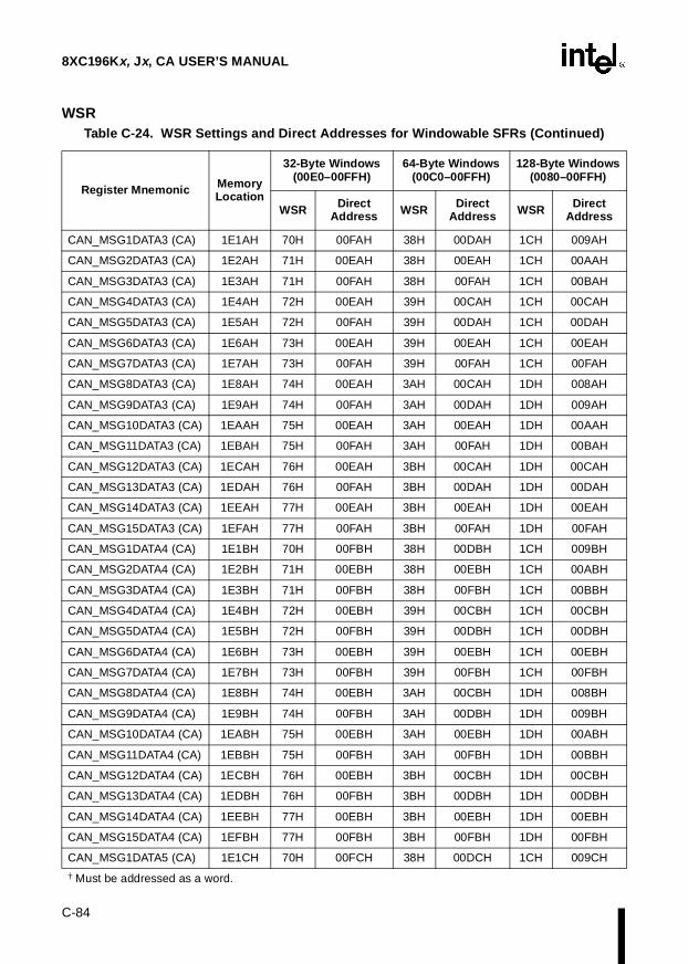
8XC196Kx, Jx, CA USER’S MANUAL
C-84
WSR
CAN_MSG1DATA3 (CA) 1E1AH 70H 00FAH 38H 00DAH 1CH 009AH
CAN_MSG2DATA3 (CA) 1E2AH 71H 00EAH 38H 00EAH 1CH 00AAH
CAN_MSG3DATA3 (CA) 1E3AH 71H 00FAH 38H 00FAH 1CH 00BAH
CAN_MSG4DATA3 (CA) 1E4AH 72H 00EAH 39H 00CAH 1CH 00CAH
CAN_MSG5DATA3 (CA) 1E5AH 72H 00FAH 39H 00DAH 1CH 00DAH
CAN_MSG6DATA3 (CA) 1E6AH 73H 00EAH 39H 00EAH 1CH 00EAH
CAN_MSG7DATA3 (CA) 1E7AH 73H 00FAH 39H 00FAH 1CH 00FAH
CAN_MSG8DATA3 (CA) 1E8AH 74H 00EAH 3AH 00CAH 1DH 008AH
CAN_MSG9DATA3 (CA) 1E9AH 74H 00FAH 3AH 00DAH 1DH 009AH
CAN_MSG10DATA3 (CA) 1EAAH 75H 00EAH 3AH 00EAH 1DH 00AAH
CAN_MSG11DATA3 (CA) 1EBAH 75H 00FAH 3AH 00FAH 1DH 00BAH
CAN_MSG12DATA3 (CA) 1ECAH 76H 00EAH 3BH 00CAH 1DH 00CAH
CAN_MSG13DATA3 (CA) 1EDAH 76H 00FAH 3BH 00DAH 1DH 00DAH
CAN_MSG14DATA3 (CA) 1EEAH 77H 00EAH 3BH 00EAH 1DH 00EAH
CAN_MSG15DATA3 (CA) 1EFAH 77H 00FAH 3BH 00FAH 1DH 00FAH
CAN_MSG1DATA4 (CA) 1E1BH 70H 00FBH 38H 00DBH 1CH 009BH
CAN_MSG2DATA4 (CA) 1E2BH 71H 00EBH 38H 00EBH 1CH 00ABH
CAN_MSG3DATA4 (CA) 1E3BH 71H 00FBH 38H 00FBH 1CH 00BBH
CAN_MSG4DATA4 (CA) 1E4BH 72H 00EBH 39H 00CBH 1CH 00CBH
CAN_MSG5DATA4 (CA) 1E5BH 72H 00FBH 39H 00DBH 1CH 00DBH
CAN_MSG6DATA4 (CA) 1E6BH 73H 00EBH 39H 00EBH 1CH 00EBH
CAN_MSG7DATA4 (CA) 1E7BH 73H 00FBH 39H 00FBH 1CH 00FBH
CAN_MSG8DATA4 (CA) 1E8BH 74H 00EBH 3AH 00CBH 1DH 008BH
CAN_MSG9DATA4 (CA) 1E9BH 74H 00FBH 3AH 00DBH 1DH 009BH
CAN_MSG10DATA4 (CA) 1EABH 75H 00EBH 3AH 00EBH 1DH 00ABH
CAN_MSG11DATA4 (CA) 1EBBH 75H 00FBH 3AH 00FBH 1DH 00BBH
CAN_MSG12DATA4 (CA) 1ECBH 76H 00EBH 3BH 00CBH 1DH 00CBH
CAN_MSG13DATA4 (CA) 1EDBH 76H 00FBH 3BH 00DBH 1DH 00DBH
CAN_MSG14DATA4 (CA) 1EEBH 77H 00EBH 3BH 00EBH 1DH 00EBH
CAN_MSG15DATA4 (CA) 1EFBH 77H 00FBH 3BH 00FBH 1DH 00FBH
CAN_MSG1DATA5 (CA) 1E1CH 70H 00FCH 38H 00DCH 1CH 009CH
Table C-24. WSR Settings and Direct Addresses for Windowable SFRs (Continued)
Register Mnemonic MemoryLocation
32-Byte Windows(00E0–00FFH)
64-Byte Windows(00C0–00FFH)
128-Byte Windows(0080–00FFH)
WSR Direct Address WSR Direct
Address WSR Direct Address
† Must be addressed as a word.
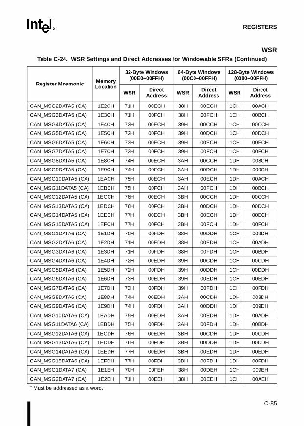
C-85
REGISTERS
WSR
CAN_MSG2DATA5 (CA) 1E2CH 71H 00ECH 38H 00ECH 1CH 00ACH
CAN_MSG3DATA5 (CA) 1E3CH 71H 00FCH 38H 00FCH 1CH 00BCH
CAN_MSG4DATA5 (CA) 1E4CH 72H 00ECH 39H 00CCH 1CH 00CCH
CAN_MSG5DATA5 (CA) 1E5CH 72H 00FCH 39H 00DCH 1CH 00DCH
CAN_MSG6DATA5 (CA) 1E6CH 73H 00ECH 39H 00ECH 1CH 00ECH
CAN_MSG7DATA5 (CA) 1E7CH 73H 00FCH 39H 00FCH 1CH 00FCH
CAN_MSG8DATA5 (CA) 1E8CH 74H 00ECH 3AH 00CCH 1DH 008CH
CAN_MSG9DATA5 (CA) 1E9CH 74H 00FCH 3AH 00DCH 1DH 009CH
CAN_MSG10DATA5 (CA) 1EACH 75H 00ECH 3AH 00ECH 1DH 00ACH
CAN_MSG11DATA5 (CA) 1EBCH 75H 00FCH 3AH 00FCH 1DH 00BCH
CAN_MSG12DATA5 (CA) 1ECCH 76H 00ECH 3BH 00CCH 1DH 00CCH
CAN_MSG13DATA5 (CA) 1EDCH 76H 00FCH 3BH 00DCH 1DH 00DCH
CAN_MSG14DATA5 (CA) 1EECH 77H 00ECH 3BH 00ECH 1DH 00ECH
CAN_MSG15DATA5 (CA) 1EFCH 77H 00FCH 3BH 00FCH 1DH 00FCH
CAN_MSG1DATA6 (CA) 1E1DH 70H 00FDH 38H 00DDH 1CH 009DH
CAN_MSG2DATA6 (CA) 1E2DH 71H 00EDH 38H 00EDH 1CH 00ADH
CAN_MSG3DATA6 (CA) 1E3DH 71H 00FDH 38H 00FDH 1CH 00BDH
CAN_MSG4DATA6 (CA) 1E4DH 72H 00EDH 39H 00CDH 1CH 00CDH
CAN_MSG5DATA6 (CA) 1E5DH 72H 00FDH 39H 00DDH 1CH 00DDH
CAN_MSG6DATA6 (CA) 1E6DH 73H 00EDH 39H 00EDH 1CH 00EDH
CAN_MSG7DATA6 (CA) 1E7DH 73H 00FDH 39H 00FDH 1CH 00FDH
CAN_MSG8DATA6 (CA) 1E8DH 74H 00EDH 3AH 00CDH 1DH 008DH
CAN_MSG9DATA6 (CA) 1E9DH 74H 00FDH 3AH 00DDH 1DH 009DH
CAN_MSG10DATA6 (CA) 1EADH 75H 00EDH 3AH 00EDH 1DH 00ADH
CAN_MSG11DATA6 (CA) 1EBDH 75H 00FDH 3AH 00FDH 1DH 00BDH
CAN_MSG12DATA6 (CA) 1ECDH 76H 00EDH 3BH 00CDH 1DH 00CDH
CAN_MSG13DATA6 (CA) 1EDDH 76H 00FDH 3BH 00DDH 1DH 00DDH
CAN_MSG14DATA6 (CA) 1EEDH 77H 00EDH 3BH 00EDH 1DH 00EDH
CAN_MSG15DATA6 (CA) 1EFDH 77H 00FDH 3BH 00FDH 1DH 00FDH
CAN_MSG1DATA7 (CA) 1E1EH 70H 00FEH 38H 00DEH 1CH 009EH
CAN_MSG2DATA7 (CA) 1E2EH 71H 00EEH 38H 00EEH 1CH 00AEH
Table C-24. WSR Settings and Direct Addresses for Windowable SFRs (Continued)
Register Mnemonic MemoryLocation
32-Byte Windows(00E0–00FFH)
64-Byte Windows(00C0–00FFH)
128-Byte Windows(0080–00FFH)
WSR Direct Address WSR Direct
Address WSR Direct Address
† Must be addressed as a word.

8XC196Kx, Jx, CA USER’S MANUAL
C-86
WSR
CAN_MSG3DATA7 (CA) 1E3EH 71H 00FEH 38H 00FEH 1CH 00BEH
CAN_MSG4DATA7 (CA) 1E4EH 72H 00EEH 39H 00CEH 1CH 00CEH
CAN_MSG5DATA7 (CA) 1E5EH 72H 00FEH 39H 00DEH 1CH 00DEH
CAN_MSG6DATA7 (CA) 1E6EH 73H 00EEH 39H 00EEH 1CH 00EEH
CAN_MSG7DATA7 (CA) 1E7EH 73H 00FEH 39H 00FEH 1CH 00FEH
CAN_MSG8DATA7 (CA) 1E8EH 74H 00EEH 3AH 00CEH 1DH 008EH
CAN_MSG9DATA7 (CA) 1E9EH 74H 00FEH 3AH 00DEH 1DH 009EH
CAN_MSG10DATA7 (CA) 1EAEH 75H 00EEH 3AH 00EEH 1DH 00AEH
CAN_MSG11DATA7 (CA) 1EBEH 75H 00FEH 3AH 00FEH 1DH 00BEH
CAN_MSG12DATA7 (CA) 1ECEH 76H 00EEH 3BH 00CEH 1DH 00CEH
CAN_MSG13DATA7 (CA) 1EDEH 76H 00FEH 3BH 00DEH 1DH 00DEH
CAN_MSG14DATA7 (CA) 1EEEH 77H 00EEH 3BH 00EEH 1DH 00EEH
CAN_MSG15DATA7 (CA) 1EFEH 77H 00FEH 3BH 00FEH 1DH 00FEH
CAN_MSG1ID0 (CA) 1E12H 70H 00F2H 38H 00D2H 1CH 0092H
CAN_MSG2ID0 (CA) 1E22H 71H 00E2H 38H 00E2H 1CH 00A2H
CAN_MSG3ID0 (CA) 1E32H 71H 00F2H 38H 00F2H 1CH 00B2H
CAN_MSG4ID0 (CA) 1E42H 72H 00E2H 39H 00C2H 1CH 00C2H
CAN_MSG5ID0 (CA) 1E52H 72H 00F2H 39H 00D2H 1CH 00D2H
CAN_MSG6ID0 (CA) 1E62H 73H 00E2H 39H 00E2H 1CH 00E2H
CAN_MSG7ID0 (CA) 1E72H 73H 00F2H 39H 00F2H 1CH 00F2H
CAN_MSG8ID0 (CA) 1E82H 74H 00E2H 3AH 00C2H 1DH 0082H
CAN_MSG9ID0 (CA) 1E92H 74H 00F2H 3AH 00D2H 1DH 0092H
CAN_MSG10ID0 (CA) 1EA2H 75H 00E2H 3AH 00E2H 1DH 00A2H
CAN_MSG11ID0 (CA) 1EB2H 75H 00F2H 3AH 00F2H 1DH 00B2H
CAN_MSG12ID0 (CA) 1EC2H 76H 00E2H 3BH 00C2H 1DH 00C2H
CAN_MSG13ID0 (CA) 1ED2H 76H 00F2H 3BH 00D2H 1DH 00D2H
CAN_MSG14ID0 (CA) 1EE2H 77H 00E2H 3BH 00E2H 1DH 00E2H
CAN_MSG15ID0 (CA) 1EF2H 77H 00F2H 3BH 00F2H 1DH 00F2H
CAN_MSG1ID1 (CA) 1E13H 70H 00F3H 38H 00D3H 1CH 0093H
CAN_MSG2ID1 (CA) 1E23H 71H 00E3H 38H 00E3H 1CH 00A3H
CAN_MSG3ID1 (CA) 1E33H 71H 00F3H 38H 00F3H 1CH 00B3H
Table C-24. WSR Settings and Direct Addresses for Windowable SFRs (Continued)
Register Mnemonic MemoryLocation
32-Byte Windows(00E0–00FFH)
64-Byte Windows(00C0–00FFH)
128-Byte Windows(0080–00FFH)
WSR Direct Address WSR Direct
Address WSR Direct Address
† Must be addressed as a word.

C-87
REGISTERS
WSR
CAN_MSG4ID1 (CA) 1E43H 72H 00E3H 39H 00C3H 1CH 00C3H
CAN_MSG5ID1 (CA) 1E53H 72H 00F3H 39H 00D3H 1CH 00D3H
CAN_MSG6ID1 (CA) 1E63H 73H 00E3H 39H 00E3H 1CH 00E3H
CAN_MSG7ID1 (CA) 1E73H 73H 00F3H 39H 00F3H 1CH 00F3H
CAN_MSG8ID1 (CA) 1E83H 74H 00E3H 3AH 00C3H 1DH 0083H
CAN_MSG9ID1 (CA) 1E93H 74H 00F3H 3AH 00D3H 1DH 0093H
CAN_MSG10ID1 (CA) 1EA3H 75H 00E3H 3AH 00E3H 1DH 00A3H
CAN_MSG11ID1 (CA) 1EB3H 75H 00F3H 3AH 00F3H 1DH 00B3H
CAN_MSG12ID1 (CA) 1EC3H 76H 00E3H 3BH 00C3H 1DH 00C3H
CAN_MSG13ID1 (CA) 1ED3H 76H 00F3H 3BH 00D3H 1DH 00D3H
CAN_MSG14ID1 (CA) 1EE3H 77H 00E3H 3BH 00E3H 1DH 00E3H
CAN_MSG15ID1 (CA) 1EF3H 77H 00F3H 3BH 00F3H 1DH 00F3H
CAN_MSG1ID2 (CA) 1E14H 70H 00F4H 38H 00D4H 1CH 0094H
CAN_MSG2ID2 (CA) 1E24H 71H 00E4H 38H 00E4H 1CH 00A4H
CAN_MSG3ID2 (CA) 1E34H 71H 00F4H 38H 00F4H 1CH 00B4H
CAN_MSG4ID2 (CA) 1E44H 72H 00E4H 39H 00C4H 1CH 00C4H
CAN_MSG5ID2 (CA) 1E54H 72H 00F4H 39H 00D4H 1CH 00D4H
CAN_MSG6ID2 (CA) 1E64H 73H 00E4H 39H 00E4H 1CH 00E4H
CAN_MSG7ID2 (CA) 1E74H 73H 00F4H 39H 00F4H 1CH 00F4H
CAN_MSG8ID2 (CA) 1E84H 74H 00E4H 3AH 00C4H 1DH 0084H
CAN_MSG9ID2 (CA) 1E94H 74H 00F4H 3AH 00D4H 1DH 0094H
CAN_MSG10ID2 (CA) 1EA4H 75H 00E4H 3AH 00E4H 1DH 00A4H
CAN_MSG11ID2 (CA) 1EB4H 75H 00F4H 3AH 00F4H 1DH 00B4H
CAN_MSG12ID2 (CA) 1EC4H 76H 00E4H 3BH 00C4H 1DH 00C4H
CAN_MSG13ID2 (CA) 1ED4H 76H 00F4H 3BH 00D4H 1DH 00D4H
CAN_MSG14ID2 (CA) 1EE4H 77H 00E4H 3BH 00E4H 1DH 00E4H
CAN_MSG15ID2 (CA) 1EF4H 77H 00F4H 3BH 00F4H 1DH 00F4H
CAN_MSG1ID3 (CA) 1E15H 70H 00F5H 38H 00D5H 1CH 0095H
CAN_MSG2ID3 (CA) 1E25H 71H 00E5H 38H 00E5H 1CH 00A5H
CAN_MSG3ID3 (CA) 1E35H 71H 00F5H 38H 00F5H 1CH 00B5H
CAN_MSG4ID3 (CA) 1E45H 72H 00E5H 39H 00C5H 1CH 00C5H
Table C-24. WSR Settings and Direct Addresses for Windowable SFRs (Continued)
Register Mnemonic MemoryLocation
32-Byte Windows(00E0–00FFH)
64-Byte Windows(00C0–00FFH)
128-Byte Windows(0080–00FFH)
WSR Direct Address WSR Direct
Address WSR Direct Address
† Must be addressed as a word.

8XC196Kx, Jx, CA USER’S MANUAL
C-88
WSR
CAN_MSG5ID3 (CA) 1E55H 72H 00F5H 39H 00D5H 1CH 00D5H
CAN_MSG6ID3 (CA) 1E65H 73H 00E5H 39H 00E5H 1CH 00E5H
CAN_MSG7ID3 (CA) 1E75H 73H 00F5H 39H 00F5H 1CH 00F5H
CAN_MSG8ID3 (CA) 1E85H 74H 00E5H 3AH 00C5H 1DH 0085H
CAN_MSG9ID3 (CA) 1E95H 74H 00F5H 3AH 00D5H 1DH 0095H
CAN_MSG10ID3 (CA) 1EA5H 75H 00E5H 3AH 00E5H 1DH 00A5H
CAN_MSG11ID3 (CA) 1EB5H 75H 00F5H 3AH 00F5H 1DH 00B5H
CAN_MSG12ID3 (CA) 1EC5H 76H 00E5H 3BH 00C5H 1DH 00C5H
CAN_MSG13ID3 (CA) 1ED5H 76H 00F5H 3BH 00D5H 1DH 00D5H
CAN_MSG14ID3 (CA) 1EE5H 77H 00E5H 3BH 00E5H 1DH 00E5H
CAN_MSG15ID3 (CA) 1EF5H 77H 00F5H 3BH 00F5H 1DH 00F5H
CAN_MSK15 (CA) 1E0CH 70H 00ECH 38H 00CCH 1CH 008CH
CAN_SGMSK (CA) 1E06H 70H 00E6H 38H 00C6H 1CH 0086H
CAN_STAT (CA) 1E01H 70H 00E1H 38H 00C1H 1CH 0081H
COMP0_CON 1F88H 7CH 00E8H 3EH 00C8H 1FH 0088H
COMP0_TIME† 1F8AH 7CH 00EAH 3EH 00CAH 1FH 008AH
COMP1_CON 1F8CH 7CH 00ECH 3EH 00CCH 1FH 008CH
COMP1_TIME† 1F8EH 7CH 00EEH 3EH 00CEH 1FH 008EH
EPA_MASK† 1FA0H 7DH 00E0H 3EH 00E0H 1FH 00A0H
EPA_MASK1 1FA4H 7DH 00E4H 3EH 00E4H 1FH 00A4H
EPA_PEND† 1FA2H 7DH 00E2H 3EH 00E2H 1FH 00A2H
EPA_PEND1 1FA6H 7DH 00E6H 3EH 00E6H 1FH 00A6H
EPA0_CON 1F60H 7BH 00E0H 3DH 00E0H 1EH 00E0H
EPA0_TIME† 1F62H 7BH 00E2H 3DH 00E2H 1EH 00E2H
EPA1_CON† 1F64H 7BH 00E4H 3DH 00E4H 1EH 00E4H
EPA1_TIME† 1F66H 7BH 00E6H 3DH 00E6H 1EH 00E6H
EPA2_CON 1F68H 7BH 00E8H 3DH 00E8H 1EH 00E8H
EPA2_TIME† 1F6AH 7BH 00EAH 3DH 00EAH 1EH 00EAH
EPA3_CON† 1F6CH 7BH 00ECH 3DH 00ECH 1EH 00ECH
EPA3_TIME† 1F6EH 7BH 00EEH 3DH 00EEH 1EH 00EEH
EPA4_CON (Kx) 1F70H 7BH 00F0H 3DH 00F0H 1EH 00F0H
Table C-24. WSR Settings and Direct Addresses for Windowable SFRs (Continued)
Register Mnemonic MemoryLocation
32-Byte Windows(00E0–00FFH)
64-Byte Windows(00C0–00FFH)
128-Byte Windows(0080–00FFH)
WSR Direct Address WSR Direct
Address WSR Direct Address
† Must be addressed as a word.

C-89
REGISTERS
WSR
EPA4_TIME† (Kx) 1F72H 7BH 00F2H 3DH 00F2H 1EH 00F2H
EPA5_CON (Kx) 1F74H 7BH 00F4H 3DH 00F4H 1EH 00F4H
EPA5_TIME† (Kx) 1F76H 7BH 00F6H 3DH 00F6H 1EH 00F6H
EPA6_CON (Kx) 1F78H 7BH 00F8H 3DH 00F8H 1EH 00F8H
EPA6_TIME† (Kx) 1F7AH 7BH 00FAH 3DH 00FAH 1EH 00FAH
EPA7_CON (Kx) 1F7CH 7BH 00FCH 3DH 00FCH 1EH 00FCH
EPA7_TIME† (Kx) 1F7EH 7BH 00FEH 3DH 00FEH 1EH 00FEH
EPA8_CON 1F80H 7CH 00E0H 3EH 00C0H 1FH 0080H
EPA8_TIME† 1F82H 7CH 00E2H 3EH 00C2H 1FH 0082H
EPA9_CON 1F84H 7CH 00E4H 3EH 00C4H 1FH 0084H
EPA9_TIME† 1F86H 7CH 00E6H 3EH 00C6H 1FH 0086H
EPAIPV 1FA8H 7DH 00E8H 3EH 00E8H 1FH 00A8H
P0_PIN 1FDAH 7EH 00FAH 3FH 00DAH 1FH 00DAH
P1_DIR 1FD2H 7EH 00F2H 3FH 00D2H 1FH 00D2H
P1_MODE 1FD0H 7EH 00F0H 3FH 00D0H 1FH 00D0H
P1_PIN 1FD6H 7EH 00F6H 3FH 00D6H 1FH 00D6H
P1_REG 1FD4H 7EH 00F4H 3FH 00D4H 1FH 00D4H
P2_DIR 1FCBH 7EH 00EBH 3FH 00CBH 1FH 00CBH
P2_MODE 1FC9H 7EH 00E9H 3FH 00C9H 1FH 00C9H
P2_PIN 1FCFH 7EH 00EFH 3FH 00CFH 1FH 00CFH
P2_REG 1FCDH 7EH 00EDH 3FH 00CDH 1FH 00CDH
P6_DIR 1FD3H 7EH 00F3H 3FH 00D3H 1FH 00D3H
P6_MODE 1FD1H 7EH 00F1H 3FH 00D1H 1FH 00D1H
P6_PIN 1FD7H 7EH 00F7H 3FH 00D7H 1FH 00D7H
P6_REG 1FD5H 7EH 00F5H 3FH 00D5H 1FH 00D5H
SBUF_RX 1FB8H 7DH 00F8H 3EH 00F8H 1FH 00B8H
SBUF_TX 1FBAH 7DH 00FAH 3EH 00FAH 1FH 00BAH
SP_BAUD† 1FBCH 7DH 00FCH 3EH 00FCH 1FH 00BCH
SP_CON 1FBBH 7DH 00FBH 3EH 00FBH 1FH 00BBH
SP_STATUS 1FB9H 7DH 00F9H 3EH 00F9H 1FH 00B9H
SSIO_BAUD 1FB4H 7DH 00F4H 3EH 00F4H 1FH 00B4H
Table C-24. WSR Settings and Direct Addresses for Windowable SFRs (Continued)
Register Mnemonic MemoryLocation
32-Byte Windows(00E0–00FFH)
64-Byte Windows(00C0–00FFH)
128-Byte Windows(0080–00FFH)
WSR Direct Address WSR Direct
Address WSR Direct Address
† Must be addressed as a word.
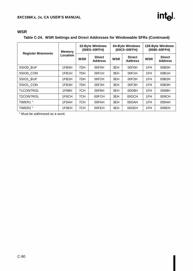
8XC196Kx, Jx, CA USER’S MANUAL
C-90
WSR
SSIO0_BUF 1FB0H 7DH 00F0H 3EH 00F0H 1FH 00B0H
SSIO0_CON 1FB1H 7DH 00F1H 3EH 00F1H 1FH 00B1H
SSIO1_BUF 1FB2H 7DH 00F2H 3EH 00F2H 1FH 00B2H
SSIO1_CON 1FB3H 7DH 00F3H 3EH 00F3H 1FH 00B3H
T1CONTROL 1F98H 7CH 00F8H 3EH 00D8H 1FH 0098H
T2CONTROL 1F9CH 7CH 00FCH 3EH 00DCH 1FH 009CH
TIMER1 † 1F9AH 7CH 00FAH 3EH 00DAH 1FH 009AH
TIMER2 † 1F9EH 7CH 00FEH 3EH 00DEH 1FH 009EH
Table C-24. WSR Settings and Direct Addresses for Windowable SFRs (Continued)
Register Mnemonic MemoryLocation
32-Byte Windows(00E0–00FFH)
64-Byte Windows(00C0–00FFH)
128-Byte Windows(0080–00FFH)
WSR Direct Address WSR Direct
Address WSR Direct Address
† Must be addressed as a word.

C-91
REGISTERS
ZERO_REG
ZERO_REG Address:Reset State:
00H0000H
The two-byte zero register (ZERO_REG) is always equal to zero. It is useful as a fixed source of the constant zero for comparisons and calculations. ZERO_REG can also be used as the WORD variable in a long-indexed reference. This combination of register selection and address mode enables direct addressing of any location in memory. A CMPL (compare long) instruction with ZERO_REG forces a compare with a “generated” 32-bit zero value.
15 8
Zero (high byte)
7 0
Zero (low byte)
Bit Number Function
15:0 Zero
This register is always equal to zero.

8XC196Kx, Jx, CA USER’S MANUAL
C-92
ZERO_REG

Glossary


Glossary-1
GLOSSARY
This glossary defines acronyms, abbreviations, and terms that have special meaning in this man-ual. (Chapter 1 discusses notational conventions and general terminology.)
absolute error The maximum difference between correspondingactual and ideal code transitions. Absolute erroraccounts for all deviations of an actual A/D converterfrom an ideal converter.
accumulator A register or storage location that forms the result ofan arithmetic or logical operation.
actual characteristic A graph of output code versus input voltage of anactual A/D converter. An actual characteristic mayvary with temperature, supply voltage, and frequencyconditions.
A/D converter Analog-to-digital converter.
ALU Arithmetic-logic unit. The part of the RALU thatprocesses arithmetic and logical operations.
assert The act of making a signal active (enabled). Thepolarity (high or low) is defined by the signal name.Active-low signals are designated by a pound symbol(#) suffix; active-high signals have no suffix. To assertRD# is to drive it low; to assert ALE is to drive ithigh.
attenuation A decrease in amplitude; voltage decay.
bit A binary digit.
BIT A single-bit operand that can take on the Booleanvalues, “true” and “false.”
break-before-make The property of a multiplexer which guarantees that apreviously selected channel is deselected before anew channel is selected. (That is, break-before-makeensures that the A/D converter will not short inputstogether.)
byte Any 8-bit unit of data.
BYTE An unsigned, 8-bit variable with values from 0through 28–1.
8XC196Kx, Jx, CA USER’S MANUAL
Glossary-2
CAN Controller area network. The 8XC196CA’s integratednetworking peripheral, similar to Intel’s standalone82527 CAN serial communications controller, thatsupports CAN specification 2.0.
CCBs Chip configuration bytes. The chip configurationregisters (CCRs) are loaded with the contents of theCCBs after a device reset, unless the device isentering programming modes, in which case thePCCBs is used.
CCRs Chip configuration registers. Registers that specifythe environment in which the device will beoperating. The chip configuration registers are loadedwith the contents of the CCBs after a device resetunless the device is entering programming modes, inwhich case the PCCBs are used.
channel-to-channel matching error The difference between corresponding codetransitions of actual characteristics taken fromdifferent A/D converter channels under the sametemperature, voltage, and frequency conditions. Thiserror is caused by differences in DC input leakage andon-channel resistance from one multiplexer channelto another.
characteristic A graph of output code versus input voltage; thetransfer function of an A/D converter.
clear The “0” value of a bit or the act of giving it a “0”value. See also set.
code 1) A set of instructions that perform a specificfunction; a program. 2) The digital value output by the A/D converter.
code center The voltage corresponding to the midpoint betweentwo adjacent code transitions on the A/D converter.
code transition The point at which the A/D converter’s output codechanges from “Q” to “Q+1.” The input voltage corre-sponding to a code transition is defined as the voltagethat is equally likely to produce either of two adjacentcodes.

Glossary-3
GLOSSARY
code width The voltage change corresponding to the differencebetween two adjacent code transitions. Code widthdeviations cause differential nonlinearity and nonlin-earity errors.
crosstalk See off-isolation.
DC input leakage Leakage current from an analog input pin to ground.
deassert The act of making a signal inactive (disabled). Thepolarity (high or low) is defined by the signal name.Active-low signals are designated by a pound symbol(#) suffix; active-high signals have no suffix. Todeassert RD# is to drive it high; to deassert ALE is todrive it low.
differential nonlinearity The difference between the actual code width and theideal one-LSB code width of the terminal-basedcharacteristic of an A/D converter. It provides ameasure of how much the input voltage may havechanged in order to produce a one-count change in theconversion result. Differential nonlinearity is ameasure of local code-width error; nonlinearity is ameasure of overall code-transition error.
doping The process of introducing a periodic table Group IIIor Group V element into a Group IV element (e.g.,silicon). A Group III impurity (e.g., indium orgallium) results in a p-type material. A Group Vimpurity (e.g., arsenic or antimony) results in an n-type material.
double-word Any 32-bit unit of data.
DOUBLE-WORD An unsigned, 32-bit variable with values from 0through 232–1.
DPRAM Dual-port RAM. A type of random-access memorycommonly used to hold shared data when using aparallel bus for communication between two CPUs.
EPA Event processor array. An integrated peripheral thatprovides high-speed input/output capability.
EPROM Erasable, programmable read-only-memory.
ESD Electrostatic discharge.

8XC196Kx, Jx, CA USER’S MANUAL
Glossary-4
feedthrough The attenuation from an input voltage on the selectedchannel to the A/D output after the sample windowcloses. The ability of the A/D converter to reject aninput on its selected channel after the sample windowcloses.
FET Field-effect transistor.
full-scale error The difference between the ideal and actual inputvoltage corresponding to the final (full-scale) codetransition of an A/D converter.
hold latency The time it takes the microcontroller to assert HLDA#after an external device asserts HOLD#.
ideal characteristic The characteristic of an ideal A/D converter. An idealcharacteristic is unique: its first code transition occurswhen the input voltage is 0.5 LSB, its full-scale (final)code transition occurs when the input voltage is 1.5LSB less than the full-scale reference, and its codewidths are all exactly 1.0 LSB. These properties resultin a conversion without zero offset, full-scale, orlinearity errors. Quantizing error is the only errorseen in an ideal A/D converter.
input leakage Current leakage from an input pin to power or ground.
input series resistance The effective series resistance from an analog inputpin to the sample capacitor of an A/D converter.
integer Any member of the set consisting of the positive andnegative whole numbers and zero.
INTEGER A 16-bit, signed variable with values from –215
through +215–1.
interrupt controller The module responsible for handling interrupts thatare to be serviced by interrupt service routines thatyou provide. Also called the programmable interruptcontroller (PIC).
interrupt latency The total delay between the time that an interrupt isgenerated (not acknowledged) and the time that thedevice begins executing the interrupt service routineor PTS routine.
interrupt service routine A software routine that you provide to service astandard interrupt. See also PTS routine.

Glossary-5
GLOSSARY
interrupt vector A location in special-purpose memory that holds thestarting address of an interrupt service routine.
ISR See interrupt service routine.
linearity errors See differential nonlinearity and nonlinearity.
LONG-INTEGER A 32-bit, signed variable with values from –231
through +231–1.
LSB 1) Least-significant bit of a byte or least-significantbyte of a word.
2) In an A/D converter, the reference voltage dividedby 2n, where n is the number of bits to be converted.For a 10-bit converter with a reference voltage of 5.12volts, one LSB is equal to 5.0 millivolts (5.12 ÷ 210)
maskable interrupts All interrupts except unimplemented opcode,software trap, and NMI. Maskable interrupts can bedisabled (masked) by the individual mask bits in theinterrupt mask registers, and their servicing can bedisabled by the global interrupt enable bit. Eachmaskable interrupt can be assigned to the PTS forprocessing.
monotonic The property of successive approximation converterswhich guarantees that increasing input voltagesproduce adjacent codes of increasing value, and thatdecreasing input voltages produce adjacent codes ofdecreasing value. (In other words, a converter ismonotonic if every code change represents an inputvoltage change in the same direction.) Large differ-ential nonlinearity errors can cause the converter toexhibit nonmonotonic behavior.
MSB Most-significant bit of a byte or most-significant byteof a word.
n-channel FET A field-effect transistor with an n-type conductingpath (channel).
n-type material Semiconductor material with introduced impurities(doping) causing it to have an excess of negativelycharged carriers.
8XC196Kx, Jx, CA USER’S MANUAL
Glossary-6
no missing codes An A/D converter has no missing codes if, for everyoutput code, there is a unique input voltage rangewhich produces that code only. Large differentialnonlinearity errors can cause the converter to misscodes.
nonlinearity The maximum deviation of code transitions of theterminal-based characteristic from the corre-sponding code transitions of the ideal characteristic.
nonmaskable interrupts Interrupts that cannot be masked (disabled) andcannot be assigned to the PTS for processing. Thenonmaskable interrupts are unimplemented opcode,software trap, and NMI.
nonvolatile memory Read-only memory that retains its contents whenpower is removed. Many MCS® 96 microcontrollersare available with either masked ROM, EPROM, orOTPROM. Consult the Automotive Products orEmbedded Microcontrollers databook to determinewhich type of memory is available for a specificdevice.
npn transistor A transistor consisting of one part p-type material andtwo parts n-type material.
off-isolation The ability of an A/D converter to reject (isolate) thesignal on a deselected (off) output.
OTPROM One-time-programmable read-only memory. Similarto EPROM, but it comes in an unwindowed packageand cannot be erased.
p-channel FET A field-effect transistor with a p-type conductingpath.
p-type material Semiconductor material with introduced impurities(doping) causing it to have an excess of positivelycharged carriers.
PC Program counter.
PCCBs Programming chip configuration bytes, which areloaded into the chip configuration registers (CCRs)when the device is entering programming modes;otherwise, the CCBs are used.

Glossary-7
GLOSSARY
PIC Programmable interrupt controller. The moduleresponsible for handling interrupts that are to beserviced by interrupt service routines that youprovide. Also called simply the interrupt controller.
prioritized interrupt Any maskable interrupt or nonmaskable NMI. Two ofthe nonmaskable interrupts (unimplemented opcodeand software trap) are not prioritized; they vectordirectly to the interrupt service routine whenexecuted.
program memory A partition of memory where instructions can bestored for fetching and execution.
protected instruction An instruction that prevents an interrupt from beingacknowledged until after the next instructionexecutes. The protected instructions are DI, EI, DPTS,EPTS, POPA, POPF, PUSHA, and PUSHF.
PSW Program status word. The high byte of the PSW is thestatus byte, which contains one bit that globallyenables or disables servicing of all maskableinterrupts, one bit that enables or disables the PTS,and six Boolean flags that reflect the state of theuser’s program. The low byte of the PSW is theINT_MASK register. A push or pop instruction savesor restores both bytes (PSW + INT_MASK).
PTS Peripheral transaction server. The microcodedhardware interrupt processor.
PTSCB See PTS control block.
PTS control block A block of data required for each PTS interrupt. Themicrocode executes the proper PTS routine based onthe contents of the PTS control block.
PTS cycle The microcoded response to a single PTS interruptrequest.
PTS interrupt Any maskable interrupt that is assigned to the PTS forinterrupt processing.
PTS mode A microcoded response that enables the PTS tocomplete a specific task quickly. These tasks includetransferring a single byte or word, transferring a blockof bytes or words, managing multiple A/D conver-sions, and generating PWM outputs.

8XC196Kx, Jx, CA USER’S MANUAL
Glossary-8
PTS routine The entire microcoded response to multiple PTSinterrupt requests. The PTS routine is controlled bythe contents of the PTS control block.
PTS transfer The movement of a single byte or word from thesource memory location to the destination memorylocation.
PTS vector A location in special-purpose memory that holds thestarting address of a PTS control block.
PWM Pulse-width modulated (outputs). The EPA can beused with or without the PTS to generate PWMoutputs.
quantizing error An unavoidable A/D conversion error that resultssimply from the conversion of a continuous voltage toits integer digital representation. Quantizing error isalways ± 0.5 LSB and is the only error present in anideal A/D converter.
RALU Register arithmetic-logic unit. A part of the CPU thatconsists of the ALU, the PSW, the master PC, themicrocode engine, a loop counter, and six registers.
repeatability error The difference between corresponding codetransitions from different actual characteristics takenfrom the same converter on the same channel with thesame temperature, voltage, and frequency conditions.The amount of repeatability error depends on thecomparator’s ability to resolve very similar voltagesand the extent to which random noise contributes tothe error.
reserved memory A memory location that is reserved for factory use orfor future expansion. Do not use a reserved memorylocation except to initialize it with FFH.
resolution The number of input voltage levels that an A/Dconverter can unambiguously distinguish between.The number of useful bits of information that theconverter can return.
sample capacitor A small (2–3 pF) capacitor used in the A/D convertercircuitry to store the input voltage on the selectedinput channel.
Glossary-9
GLOSSARY
sample delay The time period between the time that A/D converterreceives the “start conversion” signal and the timethat the sample capacitor is connected to the selectedchannel.
sample delay uncertainty The variation in the sample delay.
sample time The period of time that the sample window is open.(That is, the length of time that the input channel isactually connected to the sample capacitor.)
sample time uncertainty The variation in the sample time.
sample window The period of time that begins when the samplecapacitor is attached to a selected channel of an A/Dconverter and ends when the sample capacitor isdisconnected from the selected channel.
sampled inputs All input pins, with the exception of RESET#, aresampled inputs. The input pin is sampled one statetime before the read buffer is enabled. Samplingoccurs during PH1 (while CLKOUT is low) andresolves the value (high or low) of the pin before it ispresented to the internal bus. If the pin value changesduring the sample time, the new value may or may notbe recorded during the read.
RESET# is a level-sensitive input. EXTINT isnormally a sampled input; however, the powerdowncircuitry uses EXTINT as a level-sensitive inputduring powerdown mode.
SAR Successive approximation register. A component ofthe A/D converter.
set The “1” value of a bit or the act of giving it a “1”value. See also clear.
SFR Special-function register.
SHORT-INTEGER An 8-bit, signed variable with values from –27
through +27–1.
sign extension A method for converting data to a larger format byfilling the upper bit positions with the value of thesign. This conversion preserves the positive ornegative value of signed integers.
sink current Current flowing into a device to ground. Always apositive value.

8XC196Kx, Jx, CA USER’S MANUAL
Glossary-10
source current Current flowing out of a device from VCC. Always anegative value.
SP Stack pointer.
special interrupt Any of the three nonmaskable interrupts (unimple-mented opcode, software trap, or NMI).
special-purpose memory A partition of memory used for storing the interruptvectors, PTS vectors, chip configuration bytes, andseveral reserved locations. In previous documen-tation, this area was called reserved memory. In thismanual, reserved memory refers to locations that youshould not use for any purpose except to initializethem with FFH.
standard interrupt Any maskable interrupt that is assigned to theinterrupt controller for processing by an interruptservice routine.
state time (or state) The basic time unit of the device; the combinedperiod of the two internal timing signals, PH1 andPH2. (The internal clock generator produces PH1 andPH2 by halving the frequency of the signal onXTAL1. The rising edges of the active-high PH1 andPH2 signals generate CLKOUT, the output of theinternal clock generator.) Because the device canoperate at many frequencies, this manual defines timerequirements in terms of state times rather than inspecific units of time.
successive approximation An A/D conversion method that uses a binary searchto arrive at the best digital representation of an analoginput.
temperature coefficient Change in the stated variable for each degreeCentigrade of temperature change.
temperature drift The change in a specification due to a change intemperature. Temperature drift can be calculated byusing the temperature coefficient for the specification.
terminal-based characteristic An actual characteristic that has been translated andscaled to remove zero offset error and full-scale error.A terminal-based characteristic resembles an actualcharacteristic with zero offset error and full-scaleerror removed.
Glossary-11
GLOSSARY
transfer function A graph of output code versus input voltage; thecharacteristic of the A/D converter.
transfer function errors Errors inherent in an analog-to-digital conversionprocess: quantizing error, zero offset error, full-scaleerror, differential nonlinearity, and nonlinearity.Errors that are hardware-dependent, rather than beinginherent in the process itself, include feedthrough,repeatability, channel-to-channel matching, off-isolation, and VCC rejection errors.
UART Universal asynchronous receiver and transmitter. Apart of the serial I/O port.
VCC rejection The property of an A/D converter that causes it toignore (reject) changes in VCC so that the actualcharacteristic is unaffected by those changes. Theeffectiveness of VCC rejection is measured by the ratioof the change in VCC to the change in the actualcharacteristic.
watchdog timer An internal timer that resets the device if softwarefails to respond before the timer overflows.
WDT See watchdog timer.
word Any 16-bit unit of data.
WORD An unsigned, 16-bit variable with values from 0through 216–1.
zero extension A method for converting data to a larger format byfilling the upper bit positions with zeros.
zero offset error An ideal A/D converter’s first code transition occurswhen the input voltage is 0.5 LSB. Zero-offset error isthe difference between 0.5 LSB and the actual inputvoltage that triggers an A/D converter’s first codetransition.

8XC196Kx, Jx, CA USER’S MANUAL
Glossary-12

Index


Index-1
INDEX#, defined, 1-3, A-1
AA/D converter, 2-11, 11-1–11-19
actual characteristic, 11-17and port 0 reads, 11-14and PTS, 5-26–5-31block diagram, 11-1calculating result, 11-9, 11-14calculating series resistance, 11-11characteristics, 11-16–11-19conversion time, 11-6determining status, 11-9errors, 11-14–11-19hardware considerations, 11-11–11-14ideal characteristic, 11-16, 11-17input circuit, suggested, 11-13input protection devices, 11-13interfacing with, 11-11–11-14interpreting results, 11-9interrupt, 5-28, 5-29, 5-31, 11-9minimizing input source resistance, 11-12overview, 11-3–11-4programming, 11-4–11-9sample delay, 11-3sample time, 11-6sample window, 11-3SFRs, 11-2signals, 11-2starting with PTS, 5-26–5-31successive approximation algorithm, 11-4successive approximation register (SAR),
11-4terminal-based characteristic, 11-19threshold-detection modes, 11-6, 11-8transfer function, 11-16–11-19zero-offset adjustment, 11-3, 11-5zero-offset error, 11-17See also port 0
A/D scan mode‚ See PTSAccumulator, RALU, 2-5ACH0–ACH7, B-8
idle, powerdown, reset status, B-20ACH2–ACH7
idle, powerdown, reset status, B-21, B-22AD0–AD15, B-9AD_COMMAND, 11-8, C-80ADD instruction, A-2, A-7, A-42, A-43, A-48,
A-54ADDB instruction, A-2, A-7, A-43, A-44, A-48,
A-54ADDC instruction, A-2, A-7, A-45, A-48, A-54ADDCB instruction, A-2, A-8, A-45, A-48, A-54Address space
See memory partitionsAddress/data bus, 2-6, 15-11, 15-17
AC timing specifications, 15-36–15-40multiplexing, 15-8–15-14
Addressing modes, 3-5–3-6, A-6AD_RESULT, 5-28, 11-6, 11-10, C-80AD_TEST, 11-5, C-80AD_TIME, 11-7, C-80ADV#, B-9AINC#, 16-12, B-9ALE, 15-2, B-9
during bus hold, 15-17idle, powerdown, reset status, B-20, B-21,
B-23Analog-to-digital converter‚ See A/D converterAND instruction, A-2, A-8, A-42, A-43, A-49,
A-55ANDB instruction, A-2, A-8, A-9, A-43, A-44,
A-49, A-55ANGND, 11-5, 13-1, B-9ApBUILDER software, downloading, 1-10Application notes, ordering, 1-6Architecture
core block diagram, 2-3device block diagram, 2-3device comparison, 2-3
Arithmetic instructions, A-48, A-49, A-54, A-55Assert, defined, 1-3Auto programming mode, 16-26–16-29
algorithm, 16-29circuit, 16-26–16-27memory map, 16-28PCCB, 16-28security key programming, 16-30
Index-2
BBaud rate
SIO port, 7-10–7-12SSIO port, 8-9
Baud-rate generatorSSIO port, 8-9
BAUD_VALUE, 7-11, C-68BHE#, 15-2, B-10
during bus hold, 15-17idle, powerdown, reset status, B-20, B-23
BIT, defined, 3-2Bit-test instructions, A-17Block diagram
A/D converter, 11-1CAN peripheral, 12-2EPA, 10-2SIO port, 7-1, 10-2slave port, 9-3SSIO, 8-1
Block transfer mode‚ See PTSBMOV instruction, A-2, A-9, A-45, A-50BMOVI instruction, A-3, A-9, A-10, A-46, A-50BR (indirect) instruction, A-2, A-10, A-51, A-57BREQ#, 15-2, 15-17, B-10Bulletin board system (BBS), 1-9Bus contention, during CCB fetch, 15-9Bus contention, See address/data bus, contentionBus controller, 2-6, 15-15, 16-6
read cycles, 15-11, 15-13write cycles, 15-11, 15-13
Bus-control modes, 15-20–15-30address valid strobe, 15-26–15-28address valid with write strobe, 15-29–15-30standard, 15-20–15-23write strobe, 15-24–15-25
Bus-control signals, 15-20Bus-hold protocol, 15-17–15-20
and code execution, 15-20and interrupts, 15-20and reset, See resetdisabling, 15-19enabling, 15-18hold latency, 15-19regaining bus control, 15-20signals, 15-17signals, See also port 2, BREQ#, HLDA#,
HOLD#
software protection, 15-19timing parameters, 15-17
Bus-timing modes, 15-30–15-35comparison, 15-31, 15-32mode 0, 15-32mode 1, 15-32mode 2, 15-33mode 3, 15-32
BUSWIDTH, 15-9, 15-10, 15-23, 16-26, 16-28, B-10
and CCB fetch, 15-9idle, powerdown, reset status, B-20timing requirements, 15-10
Bus-width16-bit, 15-9, 15-11, 15-218- and 16-bit comparison, 15-8–15-148-bit, 15-9, 15-13, 15-22, 15-24dynamic 16-bit/8-bit, 15-10, 15-23selecting, 15-9, 15-10
BYTE, defined, 3-2
CCall instructions, A-51, A-57, A-58CAN serial communications controller, 2-11,
12-1–12-42address map, 12-5bit timing, 12-10–12-12block diagram, 12-2bus-off state, 12-41error detection and management logic, 12-9message
acceptance filtering, 12-6frames, 12-7
extended, 12-8standard, 12-8
identifiers, effect of masking on, 12-7objects, 12-5–12-6
overview, 12-1–12-2programming, 12-4–12-31receive and transmit priorities, 12-6registers, 12-3–12-4signals, 12-3
Carry (C) flag, 3-4, A-4, A-5, A-11, A-18, A-19, A-20, A-21, A-31
Cascading timers, 10-7CBE flag, 9-15CCB fetch

Index-3
and BHE#, 6-14and bus-width, 15-9and P5.5, 6-14and P5.6, 6-14and READY, 6-14
CCBs, 4-3, 13-8, 15-1, 15-4fetching, 15-4security-lock bits, 16-30–16-31
CCR0, 15-20CCRs, 13-8, 14-4, 15-4
security-lock bits, 16-18Chip configuration bytes, See CCBsClear, defined, 1-3CLKOUT, 14-1, 15-3, 15-11, B-10
and BUSWIDTH, 15-10and HOLD#, 15-17and internal timing, 2-7and interrupts, 5-6and READY, 15-15and RESET#, 13-9considerations, 6-13idle, powerdown, reset status, B-20, B-21,
B-22reset status, 6-7
Clockexternal, 13-7generator, 2-7, 13-7, 13-9internal
and idle mode, 14-3, 14-4phases, internal, 2-8slow, 10-7sources, 13-5
CLR instruction, A-2, A-10, A-42, A-48, A-54CLRB instruction, A-2, A-11, A-42, A-48, A-54CLRC instruction, A-3, A-11, A-47, A-53, A-59CLRVT instruction, A-3, A-11, A-47, A-53, A-59CMP instruction, A-3, A-11, A-44, A-48, A-54CMPB instruction, A-3, A-11, A-44, A-45, A-48,
A-54CMPL instruction, A-2, A-12, A-46, A-48, A-54Code execution, 2-5, 2-6Code RAM, 4-10COMP0_CON, C-88COMP0_TIME, C-88COMP1_CON, C-88COMP1_TIME, C-88CompuServe forums, 1-10Conditional jump instructions, A-5
Controlling the clock source and direction, 10-18, 10-19, C-75, C-76
CPU, 2-4CPVER, 16-12, B-11Customer service, 1-8
DData instructions, A-50, A-57Data types, 3-1–3-4
addressing restrictions, 3-1converting between, 3-4defined, 3-1iC-96, 3-1PLM-96, 3-1signed and unsigned, 3-1, 3-4values permitted, 3-1
Datasheets, online, 1-10Datasheets, ordering, 1-7Deassert, defined, 1-3DEC instruction, A-2, A-12, A-42, A-48, A-54DECB instruction, A-2, A-12, A-42, A-48, A-54DED bit, 16-6–16-8, 16-31DEI bit, 16-6–16-8, 16-18Device
clock sources, 13-5minimum hardware configuration, 13-1pin reset status, B-20, B-21, B-22programming, 16-1–16-45reset, 13-8, 13-9, 13-10, 13-11, 13-12, 15-20signal descriptions, B-8
DI instruction, A-3, A-12, A-47, A-53, A-59Direct addressing, 3-9DIV instruction, A-13, A-47, A-49, A-55DIVB instruction, A-13, A-47, A-49, A-55DIVU instruction, A-3, A-13, A-44, A-49, A-55DIVUB instruction, A-3, A-14, A-45, A-49, A-55DJNZ instruction, A-2, A-5, A-14, A-46, A-52,
A-58DJNZW instruction, A-2, A-5, A-14, A-46, A-52,
A-58DLE flag, 16-36Documents, related, 1-5–1-7DOUBLE-WORD, defined, 3-3DPTS instruction, A-3, A-15, A-46, A-53, A-59Dump-word routine, 16-25

Index-4
EEA#, 15-3, 16-13, 16-14, B-11
and P5.0, 6-13and P5.3, 6-14and programming modes, 16-14idle, powerdown, reset status, B-20, B-22,
B-23EBR (indirect) instruction, A-2ECALL instruction, A-2EE opcode, and unimplemented opcode interrupt,
A-3, A-47EI instruction, 5-11, A-3, A-15, A-47, A-53, A-59EJMP instruction, A-2Enabling a timer/counter, 10-18, 10-19, C-75,
C-76EPA, 2-10, 10-1–10-36
and PTS, 10-12block diagram, 10-2capture data overruns, 10-24, C-42capture/compare modules, 10-9
programming, 10-20choosing capture or compare mode, 10-22,
C-40compare modules
programming, 10-20configuring pins, 10-2determining event status, 10-28enabling remapping for PWM, 10-21, C-40enabling the compare function, 10-25, C-33multiplexed interrupts, 10-29re-enabling the compare event, 10-22, 10-25,
C-33, C-41resetting the timer in compare mode, 10-24,
C-42resetting the timers, 10-23, 10-26, C-34, C-42selecting the capture/compare event, 10-22,
C-41selecting the compare event, 10-25, C-33selecting the time base, 10-21, 10-25, C-33,
C-40shared output pins, 10-10starting an A/D conversion, 10-23, 10-26,
C-33, C-41using for PWM, 5-31, 5-37See also port 1, port 6, PWM, timer/counters
EPA0–3, EPA8–9, B-11EPA0_CON, C-88
EPA0–EPA9, 10-3, B-11EPA0_TIME, C-88EPA1_CON, 10-21, C-40, C-88EPA1_TIME, C-88EPA2_CON, C-88EPA2_TIME, C-88EPA3_CON, 10-21, C-40, C-88EPA3_TIME, C-88EPA4_CON, C-88, C-89EPA4_TIME, C-89EPA5_TIME, C-89EPA6_TIME, C-89EPA7_CON, C-89EPA7_TIME, C-89EPA8_CON, C-89EPA8_TIME, C-89EPA9_CON, C-89EPA9_TIME, C-89EPAIPV, 5-4, 10-4, 10-29, 10-30, C-89EPA_MASK, 10-3, C-88EPA_MASK1, 10-3, C-88EPA_PEND, 10-3, C-88EPA_PEND1, 10-4, C-88EPAx interrupts
and TIJMP, 10-29, 10-31EPAx_CON, 10-4
settings and operations, 10-20EPAx_TIME, 10-4EPTS instruction, 5-11, A-15, A-46, A-53, A-59ESD protection, 6-2, 6-7, 6-16, 13-5Event, 10-1Event processor array‚ See EPAEXT instruction, A-2, A-15, A-42, A-48, A-54EXTB instruction, A-2, A-16, A-42, A-48, A-54EXTINT, 5-3, 14-1, 14-6, B-12
and powerdown mode, 14-4, 14-5, 14-6hardware considerations, 14-7
FFaxBack service, 1-8FE opcode
and inhibiting interrupts, 5-8Floating point library, 3-4Formulas
A/D conversion result, 11-9, 11-14A/D error, 11-12A/D series resistance, 11-11
Index-5
A/D threshold voltage, 11-6A/D voltage drop, 11-12capacitor size (powerdown circuit), 14-8programming voltage, 16-16PWM duty cycle, 5-32PWM frequency, 5-32SIO baud rate, 7-11, C-68
FPAL-96, 3-4Frequency
external crystal, 16-32SSIO port baud-rate generator, 8-9
GGO command, RISM, 16-35
HHandbooks, ordering, 1-6Handshaking
SSIO, 8-6Hardware
A/D converter considerations, 11-11–11-14addressing modes, 3-5auto programming circuit, 16-27clock sources, 13-5device considerations, 13-1–13-12device reset, 13-8, 13-10, 13-11, 13-12interrupt processor, 2-6, 5-1memory protection, 16-7, 16-18minimum configuration, 13-1NMI considerations, 5-6noise protection, 13-4oscillator failure detection, 16-8pin reset status, B-20, B-21, B-22programming mode requirements, 16-14reset instruction, 3-11serial port programming circuit, 16-33SIO port considerations, 7-7slave port connections, 9-6–9-7slave programming circuit, 16-17UPROM considerations, 16-7
HLDA#, 15-3, 15-17, B-12HLDA# considerations, 6-13HLDEN bit, 15-19Hold latency, See bus-hold protocolHOLD#, 15-3, 15-17, B-12HOLD# considerations, 6-12
Hypertext manuals and datasheets, downloading, 1-10
II/O ports
unused inputs, 13-2I/O ports‚ See ports‚ SIO port‚ SSIO portIBE flag, 9-5, 9-14, 9-15IBSP196, 16-32Idle mode, 2-12, 13-12, 14-3–14-4
entering, 14-4exiting, 14-4pin status, B-20, B-21, B-22timeout control, 10-7
IDLPD #1, 14-4IDLPD #2, 14-5IDLPD instruction, A-2, A-16, A-47, A-53, A-59
illegal operand, 13-9, 13-12Immediate addressing, 3-6INC instruction, A-2, A-16, A-42, A-48, A-54INCB instruction, A-2, A-17, A-42, A-48, A-54Indexed addressing, 3-9
and register RAM, 4-12and windows, 4-23
Indirect addressing, 3-6and register RAM, 4-12with autoincrement, 3-7
Input pinslevel-sensitive, B-8sampled, B-8
INST, 15-3idle, powerdown, reset status, B-20
Instruction set, 3-1and PSW flags, A-5code execution, 2-5, 2-6conventions, 1-3execution times, A-54–A-55lengths, A-48–A-54opcode map, A-2–A-3opcodes, A-42–A-47overview, 3-1–3-4protected instructions, 5-8reference, A-1–A-3See also RISM
INTEGER, defined, 3-3Interrupts, 5-1–5-41
and bus-hold, See bus-hold protocol

Index-6
controller, 2-6, 5-1end-of-PTS, 5-19inhibiting, 5-8latency, 5-7–5-10, 5-24
calculating, 5-9multiplexed, 10-29
priorities, 10-30pending registers‚ See EPA_PEND,
EPA_PEND1, INT_PEND, INT_PEND1
priorities, 5-4, 5-5modifying, 5-14–5-16
procedures, PLM-96, 3-11processing, 5-2programming, 5-11–5-16selecting PTS or standard service, 5-11service routine
processing, 5-15sources, 5-5unused inputs, 13-2vectors, 5-1, 5-5vectors, memory locations, 4-3, 4-4
INT_MASK, 10-4, 14-2INT_MASK1, 5-4INT_PEND, 10-4, 14-2INT_PEND1, 5-4Italics, defined, 1-3
JJBC instruction, A-2, A-5, A-17, A-42, A-52, A-58JBS instruction, A-3, A-5, A-17, A-42, A-52, A-58JC instruction, A-3, A-5, A-18, A-46, A-52, A-58JE instruction, A-3, A-5, A-18, A-46, A-52, A-58JGE instruction, A-2, A-5, A-18, A-46, A-52, A-58JGT instruction, A-2, A-5, A-19, A-46, A-52, A-58JH instruction, A-3, A-5, A-19, A-46, A-52, A-58JLE instruction, A-3, A-5, A-19, A-46, A-52, A-58JLT instruction, A-3, A-5, A-20, A-46, A-52, A-58JNC instruction, A-2, A-5, A-20, A-46, A-52,
A-58JNE instruction, A-2, A-5, A-20, A-46, A-52, A-58JNH instruction, A-2, A-5, A-21, A-46, A-52,
A-58JNST instruction, A-2, A-5, A-21, A-46, A-52,
A-58JNV instruction, A-2, A-5, A-21, A-46, A-52,
A-58
JNVT instruction, A-2, A-5, A-22, A-46, A-52, A-58
JST instruction, A-3, A-5, A-22, A-46, A-52, A-58Jump instructions, A-57
conditional, A-5, A-52, A-58unconditional, A-51
JV instruction, A-3, A-5, A-22, A-46, A-52, A-58JVT instruction, A-3, A-5, A-23, A-46, A-52, A-58
LLatency‚ See hold latency‚ interrupt latencyLCALL instruction, A-3, A-23, A-46, A-51LD instruction, A-2, A-23, A-45, A-50, A-57LDB instruction, A-2, A-23, A-45, A-50, A-57LDBSE instruction, A-3, A-24, A-45, A-50, A-57LDBZE instruction, A-3, A-24, A-45, A-50, A-57Level-sensitive input, B-8Literature, 1-11LJMP instruction, A-2, A-24, A-51, A-57Logical instructions, A-49, A-55LONG-INTEGER, defined, 3-4Lookup tables, software protection, 3-11
MManual contents, summary, 1-1Manuals, online, 1-10Measurements, defined, 1-5Memory bus, 2-6Memory controller, 2-4, 2-6Memory map, 4-1, 4-2, 16-1Memory mapping
auto programming mode, 16-28serial port programming mode, 16-34
Memory partitions, 4-1–4-23chip configuration bytes, 4-4chip configuration registers, 4-4internal (code) RAM, 4-10interrupt and PTS vectors, 4-4map, 4-2OTPROM, 16-2peripheral SFRs, 4-6program memory, 4-3, 16-2register file, 4-10register RAM, 4-12reserved memory, 4-4security key, 4-4SFRs, 4-5

Index-7
special-purpose memory, 4-3, 16-2Memory protection, 16-3–16-7
CCR security-lock bits, 16-18UPROM security bits, 16-7
Memory space, See memory partitionsMemory, external, 15-1–15-40
interface signals, 15-1See also address/data bus, bus controller,
bus-control modes, bus-control signals, bus-hold protocol, bus-width, BUSWIDTH, CCRs, ready control, timing, wait states
Microcode engine, 2-4Miller effect, 13-8Mode 0
bus-timing mode, 15-32SIO port mode, 7-5
Mode 1bus-timing mode, 15-32SIO port mode, 7-6
Mode 2bus-timing mode, 15-33SIO port mode, 7-6, 7-7, 7-8
Mode 3bus-timing mode, 15-32SIO port mode, 7-6, 7-7, 7-8
Modified quick-pulse algorithm, 16-10MUL instruction, A-24, A-25, A-47, A-49, A-55MULB instruction, A-25, A-47, A-49, A-55Multiprocessor communications, 2-9, 2-10
methods, 2-10, 9-1SIO port, 7-7, 7-8slave port, 9-1
MULU instruction, A-3, A-25, A-26, A-43, A-47, A-49, A-55
MULUB instruction, A-3, A-26, A-43, A-44, A-49, A-55
NNaming conventions, 1-3–1-4NEG instruction, A-2, A-26, A-42, A-49, A-55Negative (N) flag, A-4, A-5, A-18, A-19, A-20NEGB instruction, A-2, A-27, A-42, A-49, A-55NMI, 5-3, 5-4, 5-6, B-13
and bus-hold protocol, 15-20hardware considerations, 5-6idle, powerdown, reset status, B-20, B-23
Noise, reducing, 6-2, 6-3, 6-7, 11-3, 11-13, 11-14, 13-4, 13-5, 13-6
NOP instruction, 3-11, A-3, A-27, A-47, A-53, A-59
two-byte‚ See SKIP instructionNORML instruction, 3-4, A-3, A-27, A-42, A-53,
A-59NOT instruction, A-2, A-27, A-42, A-49, A-55Notational conventions, 1-3–1-4NOTB instruction, A-2, A-28, A-42, A-49, A-55Numbers, conventions, 1-4
OOBF flag, 9-5, 9-14, 9-15OFD bit, 16-8ONCE mode, 2-11, 14-9
exiting, 14-9Opcodes, A-42
EE, and unimplemented opcode interrupt, A-3, A-47
FE, and signed multiply and divide, A-3map, A-2reserved, A-3, A-47
Operand types, See data types, 3-1Operands, addressing, 3-10Operating modes, 2-11–2-12OR instruction, A-2, A-28, A-44, A-49, A-55ORB instruction, A-2, A-28, A-44, A-49, A-55Oscillator
and powerdown mode, 14-4detecting failure, 13-9, 13-12external crystal, 13-7on-chip, 13-5
OTPROMcontrolling access to internal memory,
16-4–16-6controlling fetches from external memory,
16-6–16-7enabling oscillator failure detection circuitry,
16-8memory map, 16-2programming, 16-1–16-45
See also programming modesROM-dump mode, 16-31verifying, 16-31
Overflow (V) flag, A-4, A-5, A-21, A-22
Index-8
Overflow-trap (VT) flag, A-4, A-5, A-11, A-22, A-23
PP0.0–P0.7
idle, powerdown, reset status, B-20P0.2–P0.7
idle, powerdown, reset status, B-21, B-22P0.4–P0.7
and programming modes, 16-14P0_PIN, C-89P1.0–P1.3, B-13
idle, powerdown, reset status, B-21P1.0–P1.7, B-13
idle, powerdown, reset status, B-20, B-22P1_DIR, C-89P1_MODE, C-89P1_PIN, C-89P1_REG, C-89P2.0–P2.7, B-14P2.2 considerations, 14-7P2.7 reset status, 6-7P2_DIR, C-89P2_MODE, C-89P2_PIN, C-89P2_REG, C-89P3.0–P3.7, B-14
idle, powerdown, reset status, B-20, B-21, B-22
See also port 3P4.0–P4.7, B-14
idle, powerdown, reset status, B-20, B-21, B-22
See also port 4P5.0–P5.7, B-14
idle, powerdown, reset status, B-20, B-21, B-23
P6.0–P6.7, B-15idle, powerdown, reset status, B-20, B-21,
B-23P6_DIR, C-89P6_MODE, C-89P6_PIN, C-89P6_REG, C-89PACT#, B-15PALE#, 16-8, 16-11, 16-12, B-15Parameters, passing to subroutines, 3-10
Parity, 7-6, 7-7PBUS, 16-13PBUS0–PBUS15, B-15PC (program counter), 2-4, 2-6PD bit, 14-4Peripherals, internal, 2-8Pin diagrams, B-3, B-5, B-7PLM-96
conventions, 3-9, 3-10, 3-11interrupt procedures, 3-11
PMODE, 16-11, 16-14and programming modes, 16-14
PMODE0–PMODE3, B-15POP instruction, A-3, A-28, A-46, A-50, A-56POPA instruction, A-2, A-29, A-47, A-50, A-56POPF instruction, A-2, A-29, A-47, A-50, A-56Port 0, 6-1, 6-2
considerations, 6-3, 11-14, 13-5idle, reset, powerdown status, B-20initializing, 6-10input only pins, 6-2overview, 6-1pin configuration
example, 6-11structure, 6-3
Port 1, B-13considerations, 6-12idle, powerdown, reset status, B-20, B-21,
B-22initializing, 6-10input buffer, 6-7logic tables, 6-9operation, 6-4, 6-9overview, 6-1pin configuration, 6-10, 6-12
example, 6-11SFRs, 6-5, 6-6, 10-4, 10-5structure, 6-8
Port 2, 14-2, B-14considerations, 6-12initializing, 6-10logic tables, 6-9operation, 6-4, 6-9overview, 6-1pin configuration, 6-10, 6-12
example, 6-11SFRs, 6-5, 6-6, 14-2structure, 6-8
Index-9
Port 3addressing, 6-15configuration, 6-18configuring for slave port, 9-14idle, powerdown, reset status, B-20, B-21,
B-22operation, 6-16–6-18overview, 6-1pin configuration, 6-12, 6-15structure, 6-17
Port 4addressing, 6-15configuration, 6-18idle, powerdown, reset status, B-20, B-21,
B-23operation, 6-16–6-18overview, 6-1pin configuration, 6-12, 6-15structure, 6-17
Port 5, B-14configuring for slave port, 9-14considerations, 6-13idle, powerdown, reset status, B-20initializing, 6-10logic tables, 6-9operation, 6-4, 6-9, 6-13overview, 6-1pin configuration, 6-10, 6-12, 6-13
example, 6-11SFRs, 6-5, 6-6, 10-4, 14-2structure, 6-8
Port 6, B-15considerations, 6-14initializing, 6-10logic tables, 6-9operation, 6-4overview, 6-1pin configuration, 6-10, 6-12
example, 6-11SFRs, 6-5, 6-6, 10-4, 10-5structure, 6-8
Port, serial‚ See SIO portPort, slave‚ See slave portPort, synchronous serial,See SSIO portPorts, 2-9Power and ground pins
minimum hardware connections, 13-5Power consumption, reducing, 2-12, 14-4
Powerdown mode, 2-11, 2-12, 14-4–14-7circuitry
external, 14-7, 14-8disabling, 14-4entering, 14-5exiting with EXTINT, 14-6–14-9exiting with VPP, 14-5pin status, B-20, B-21, B-22
Powerdown sequence, programming modes, 16-15Power-up sequence, programming modes, 16-15Prefetch queue, 2-6Priority encoder, 5-4Processor status word‚ See PSWProduct information, ordering, 1-6PROG#, 16-11, 16-12, B-15Program counter‚ See PCProgramming modes, 16-1–16-45
algorithms, 16-21, 16-22, 16-24, 16-29auto, 16-2entering, 16-14, 16-15exiting, 16-15hardware requirements, 16-14pin functions, 16-11–16-13selecting, 16-14serial port, 16-2slave, 16-2
Programming voltages, 13-1, 14-2, 16-13, B-18calculating, 16-16
Program-word routine, 16-23PSW, 2-4, 3-11, 5-13
flags, and instructions, A-5PTS, 2-4, 2-6, 2-11, 5-1
A/D scan mode, 5-26–5-31and A/D converter, 5-26, 5-27and EPA, 5-31–5-41and SSIO handshaking, 8-6and SSIO port, 8-5, 8-6block transfer mode, 5-24cycle execution time, 5-10cycle, defined, 5-24interrupt latency, 5-10interrupt processing flow, 5-2PWM modes, 5-31–5-41PWM remap mode, 5-37PWM toggle mode, 5-32, 10-15, 10-16single transfer mode, 5-21vectors, memory locations, 4-3, 4-4See also PWM

Index-10
PTS control block‚ See PTSCBPTS instructions, A-53, A-59PTSCB, 5-1, 5-4, 5-7, 5-8, 5-19, 5-24
memory locations, 4-4PTSSEL, 5-7, 5-11, 5-19PTSSRV, 5-7, 5-19PUSH instruction, A-3, A-29, A-46, A-50, A-56PUSHA instruction, A-2, A-30, A-47, A-50, A-56PUSHF instruction, A-2, A-30, A-47, A-50, A-56PVER, 16-10, 16-12, B-16PWM, 5-31
and cascading timer/counters, 10-7calculating duty cycle, 5-32calculating frequency, 5-32generating, 10-16modes, 5-31–5-41remap mode, 5-37toggle mode, 5-32waveform, 5-32with dedicated timer/counter, 10-16See also EPA‚ PTS
QQuick reference guides, ordering, 1-7
RRALU, 2-4–2-6RAM, internal
and serial port programming mode, 16-35RD#, 15-3, B-16
considerations, 6-14during bus hold, 15-17idle, powerdown, reset status, B-20, B-21,
B-23READY, 15-4, 15-14–15-16, 16-26, B-16
and wait states, 15-15considerations, 6-14idle, powerdown, reset status, B-20, B-23timing requirements, 15-15
Ready control, 15-14–15-16REAL variables, 3-4Reduced instruction set monitor‚ See RISMRegister bits
naming conventions, 1-4reserved, 1-4
Register file, 2-4, 4-10and windowing, 4-10, 4-13
See also windowsRegister RAM, 4-12, 5-19
and powerdown mode, 14-3, 14-4Register-direct addressing, 3-6, 3-9, 4-12
and register RAM, 4-12and windows, 4-13, 4-23
RegistersAD_COMMAND, 11-2AD_RESULT, 11-2AD_TEST, 11-2, 11-5AD_TIME, 11-2allocating, 3-10CAN_BTIME0, 12-3CAN_BTIME1, 12-3CAN_CON, 12-3CAN_EGMSK, 12-3CAN_INT, 5-3, 12-3CAN_MSGxCFG, 12-3CAN_MSGxCON0, 12-3CAN_MSGxCON1, 12-4CAN_MSGxDATAx, 12-4CAN_MSGxID, 12-4CAN_MSK15, 12-4CAN_SGMSK, 12-4CAN_STAT, 12-4INT_MASK, 5-4, 5-11, 5-15, 11-2, 16-35INT_MASK1, 5-4, 5-11, 5-15, 7-2, 8-2, 8-13,
9-4, 16-35INT_PEND, 5-4, 5-16, 11-2INT_PEND1, 5-4, 5-16, 7-2, 8-3, 8-8, 9-4, 9-5naming conventions, 1-4P0_PIN, 6-2, 6-3, 11-3P1_MODE
considerations, 6-12P2_DIR, 7-3P2_MODE, 7-3
considerations, 6-12, 6-13P2_PIN, 7-3, 8-3P2_REG, 7-3
considerations, 6-13P34_DRV, 6-16, 6-18P3_PIN, 9-2, 9-5P3_REG, 9-2, 9-5P5_MODE
considerations, 6-13, 6-14P6_DIR, 7-3P6_MODE, 7-3
considerations, 6-15

Index-11
P6_PIN, 7-3P6_REG, 7-3
considerations, 6-15PPW, 16-8, 16-9, 16-35PSW, 5-4, 5-15PTSCON, 5-21PTSCOUNT, 5-19PTSSEL, 5-4PTSSRV, 5-4Px_DIR, 6-5, 6-9, 6-10, 6-11Px_MODE, 6-5, 6-9, 6-10, 6-11Px_PIN, 6-5, 6-7, 6-9, 6-16, 6-18Px_REG, 6-5, 6-9, 6-10, 6-11, 6-16, 6-17,
6-18RALU, 2-4, 2-5, 4-12SBUF_RX, 7-3SBUF_TX, 7-3SLP_CMD, 9-2, 9-5SLP_CON, 9-5, 9-14, 9-15SLP_STAT, 9-2, 9-5, 9-14, 9-15, 9-16SP_BAUD, 7-4, 7-10, 16-35SP_CON, 7-4, 7-9, 16-35SP_PPW, 16-8, 16-9SP_STATUS, 7-4, 7-13SSIO0_BUF, 8-3, 8-5SSIO0_CON, 8-3
configuring for handshaking, 8-6SSIO1_BUF, 8-3SSIO1_CON, 8-3
configuring for handshaking, 8-6SSIO_BAUD, 8-3, 8-9SSIOx_BUF, 8-8SSIOx_CON, 8-10using, 3-9WSR, 4-14, 5-15
Reserved bits, defined, 1-4Reset, 13-9, 15-4
and bus-hold protocol, 15-20and CCB fetches, 4-4circuit diagram, 13-11status
CLKOUT/P2.7, 6-7, 6-13I/O and control pins, B-20, B-21, B-22
with illegal IDLPD operand, 13-12with RESET# pin, 13-10with RST instruction, 13-9, 13-12with watchdog timer, 13-12
RESET#, 13-1, 14-2, B-16
and CCB fetch, 13-8and CLKOUT, 13-9and device reset, 13-8, 13-9, 13-10, 15-20and ONCE mode, 14-9and powerdown mode, 14-6and programming modes, 16-14idle, powerdown, reset status, B-20, B-22,
B-23Resonator, ceramic, 13-7RET instruction, A-2, A-30, A-46, A-51RISM, 16-34, 16-35
defaults, 16-34, 16-35examples
beginning execution, 16-42loading program into RAM, 16-40programming the PPW, 16-39reading the OTPROM, 16-40setting the PC, 16-42writing to OTPROM, 16-43
ROM-dump mode, 16-31security key verification, 16-31
RS-232C interface, 16-32RST instruction, 3-11, 13-9, 13-12, A-3, A-31,
A-47, A-53, A-59Run-time programming, 16-44–16-45
code example, 16-45RXCAN, B-16RXD, 7-2, 16-12, B-16
and SIO port mode 0, 7-4and SIO port modes 1, 2, and 3, 7-6
SSampled input, 15-9, B-8SBUF_RX, C-89SBUF_TX, C-89SC0, 8-5, B-16
configuring for handshaking, 8-6SC1, 8-5, B-16
configuring for handshaking, 8-6SCALL instruction, A-3, A-31, A-42, A-48, A-51SD0, 8-5, B-16SD1, 8-5, B-16Security key
and serial port programming mode, 16-32verification, 16-31
Selecting up or down counting, 10-18, 10-19, C-75, C-76
Index-12
Serial I/O port‚ See SIO portSerial port programming mode, 16-32–16-43
circuit, 16-33defaults, 16-34, 16-35functions, 16-32memory map, 16-34operation, 16-36RISM code examples, 16-38using internal RAM, 16-35VPP voltage, 16-32See also RISM
SETC instruction, A-3, A-31, A-47, A-53, A-59SFRs
and powerdown mode, 14-3, 14-4CPU, 4-13memory-mapped, 4-5peripheral, 4-5, 4-6
and windowing, 4-13reserved, 3-10, 4-5, 4-13with indirect or indexed operations, 3-10, 4-5,
4-13with read-modify-write instructions, 4-5
Shift instructions, A-53, A-59SHL instruction, A-3, A-32, A-42, A-53, A-59SHLB instruction, A-3, A-32, A-42, A-53, A-59SHLL instruction, A-3, A-33, A-42, A-53SHORT-INTEGER, defined, 3-2SHR instruction, A-3, A-33, A-42, A-53, A-59SHRA instruction, A-3, A-34, A-42, A-53, A-59SHRAB instruction, A-3, A-34, A-42, A-53, A-59SHRAL instruction, A-3, A-35, A-42, A-53, A-59SHRB instruction, A-3, A-35, A-42, A-53, A-59SHRL instruction, A-3, A-36, A-42, A-53, A-59Signals
descriptions, B-8–B-19functional listings, B-2, B-4, B-6name changes, B-1naming conventions, 1-4
Single transfer mode‚ See PTSSIO port, 2-9, 7-1
9-bit data‚ See mode 2‚ mode 3block diagram, 7-1, 10-2calculating baud rate, 7-11, 7-12, C-68downloading to OTPROM‚ See serial port
programming modeenabling interrupts, 7-12enabling parity, 7-8–7-10framing error, 7-14
half-duplex considerations, 7-7interrupts, 7-6, 7-8, 7-14mode 0, 7-4–7-5mode 1, 7-6mode 2, 7-6, 7-7mode 3, 7-6, 7-7multiprocessor communications, 7-7, 7-8overrun error, 7-14programming, 7-8programming mode‚ See serial port
programming modereceive interrupt (RI) flag, 7-14receive register‚ See registers, SBUF_RXreceived bit 8 (RB8) flag, 7-14received parity error (RPE) flag, 7-14receiver, 7-1selecting baud rate, 7-10–7-12SFRs, 7-2signals, 7-2status, 7-13–7-14transmit interrupt (TI) flag, 7-14transmit register‚ See registers, SBUF_TXtransmitter, 7-1transmitter empty (TXE) flag, 7-14See also mode 0‚ mode 1‚ mode 2‚ mode 3‚
port 2SJMP instruction, A-2, A-36, A-42, A-48, A-51,
A-57SKIP instruction, A-2, A-36, A-42, A-53, A-59Slave port, 2-10, 9-1–9-16
address/data bus, 9-2and demultiplexed bus, 9-6and multiplexed bus, 9-6, 9-11block diagram, 9-3code examples
master program, 9-8, 9-11Port 3 configuration, 9-14Port 5 configuration, 9-14SFR initialization, 9-14slave program, 9-9, 9-12
configuring pins, 9-14determining status, 9-16hardware connections, 9-6–9-7initializing SFRs, 9-14interrupts, 9-8, 9-16
CBF interrupt, 9-16IBF interrupt, 9-16OBE interrupt, 9-16
Index-13
modes, 9-8–9-13overview, 9-2–9-5programming
SLP_CON register, 9-14–9-16programming SFRs, 9-14selecting data or command and status
registers, 9-15, C-65SFRs, 9-3shared memory mode, 9-11–9-13signals, 9-3standard slave mode, 9-8–9-13synchronizing master and slave, 9-16using with external memory, 9-2
Slave programming mode, 16-15–16-25address/command decoder routine, 16-20,
16-21algorithm, 16-20–16-25circuit, 16-16–16-17dump-word routine, 16-20, 16-24entering, 16-20program-word routine, 16-20, 16-22security key programming, 16-15timings, 16-23, 16-25
SLP0–SLP7, 9-4, B-17SLPALE, 9-4, B-17SLPCS#, 9-2, 9-4, B-17SLPINT, 9-4, B-17
considerations, 6-14idle, powerdown, reset status, B-20
SLPRD#, 9-2, 9-4, B-17SLPWR#, 9-4, B-17Software
addressing modes, 3-9conventions, 3-9–3-11device reset, 13-12IBSP196, 16-32interrupt service routines, 5-15linking subroutines, 3-10protection, 3-11, 15-19
Software trap interrupt, 5-4, 5-6, 5-8SP_BAUD, 7-10, 16-32, 16-35, C-89SP_CON, 7-9, 16-35, C-89Special instructions, A-53, A-59Special operating modes
SFRs, 14-2SP_STATUS, 7-13, C-89SSIO port, 2-9
and PTS, 8-6
block diagram, 8-1configuring port pins, 8-9enabling interrupts, 8-13handshaking, 8-6, 8-7
configuring, 8-6flow diagram, 8-7
modes, 8-3–8-6overview, 8-1programming considerations, 8-13programming example, 8-15SFRs, 8-2signals, 8-2timing diagrams, 8-6
SSIO0_BUF, C-90SSIO0_CON, C-90SSIO1_BUF, C-90SSIO1_CON, C-90SSIO_BAUD, C-89ST instruction, A-2, A-37, A-45, A-46, A-50, A-57Stack instructions, A-50, A-56Stack pointer, 4-12
and subroutine call, 4-12initializing, 4-12
State time, defined, 2-8STB instruction, A-2, A-37, A-46, A-50, A-57Sticky bit (ST) flag, 3-4, A-4, A-5, A-21, A-22SUB instruction, A-3, A-37, A-43, A-48, A-54SUBB instruction, A-3, A-38, A-43, A-44, A-48,
A-54SUBC instruction, A-3, A-38, A-45, A-48, A-54SUBCB instruction, A-3, A-38, A-45, A-48, A-54Subroutines
linking, 3-10nested, 4-12
Synchronous serial I/O port‚ See SSIO port
TT1CLK, 7-2, 10-3, B-17T1CONTROL, 10-5, C-90T1DIR, 10-3, B-18T2CLK, 10-3, B-17T2CONTROL, 10-5, C-90T2DIR, 10-3, B-18Technical support, 1-11Terminology, 1-3TIJMP instruction, A-2, A-39, A-46, A-51, A-57
and EPAx interrupt, 10-29, 10-31

Index-14
Timer, watchdog‚ See watchdog timerTimer/counters, 2-10, 10-6, 10-7
and PWM, 10-14, 10-15, 10-16cascading, 10-7configuring pins, 10-2count rate, 10-7resolution, 10-7SFRs, 10-3See also EPA
TIMER1, 10-5, C-90TIMER2, 10-5, C-90Timing
BUSWIDTH, 15-10dump-word routine, 16-25HLDA#, 15-17HOLD#, 15-17instruction execution, A-54–A-55internal, 2-7, 2-8interrupt latency, 5-7–5-10, 5-24program-word routine, 16-23PTS cycles, 5-10READY, 15-15selectable bus-timing
See bus-timing modesSIO port mode 0, 7-5SIO port mode 1, 7-6SIO port mode 2, 7-7SIO port mode 3, 7-7slave port, 9-10, 9-13slave programming routines, 16-23, 16-25write-strobe mode, 15-24
Training, 1-11TRAP instruction, 5-6, A-2, A-40, A-47, A-51TXCAN, B-18TXD, 7-2, 16-12, B-18
and SIO port mode 0, 7-4
UUART, 2-9, 7-1Unimplemented opcode interrupt, 3-11, 5-4, 5-6,
5-8Units of measure, defined, 1-5Universal asynchronous receiver and transmitter‚
See UARTUPROM, 16-6
programming, 16-6–16-7USFR, 16-7
VVCC, 13-1, B-18
and programming modes, 16-14VPP, 13-1, 14-2, 16-13, B-18
and programming modes, 16-14hardware considerations, 14-7idle, powerdown, reset status, B-20, B-22,
B-23VREF, 11-5, 13-1, B-18VSS, 13-1, B-18
and programming modes, 16-14
WWait states, 15-14–15-16
controlling, 15-15Watchdog timer, 2-11, 3-11, 3-12, 13-9, 13-12
and idle mode, 14-4WDE bit, 13-12Window selection register, See WSRWindowing, 4-13–4-23
examples, 4-20–4-23 See also windows
Windows, 4-13–4-23addressing, 4-20, 4-21and addressing modes, 4-23and memory-mapped SFRs, 4-18base address, 4-17, 4-20locations that cannot be windowed, 4-18offset address, 4-17selecting, 4-14setting up with linker loader, 4-21WSR values and direct addresses, 4-18
WORD, defined, 3-2World Wide Web, 1-10WR#, 15-4, B-18
during bus hold, 15-17idle, powerdown, reset status, B-20, B-21,
B-23WRH#, 15-2, 15-4, B-19Write-strobe mode timing, 15-24WRL#, 15-4, B-19WSR, 4-14, 15-19
XX, defined, 1-5XCH instruction, A-2, A-3, A-40, A-42, A-50,
A-57

Index-15
XCHB instruction, A-2, A-3, A-40, A-42, A-50, A-57
XOR instruction, A-2, A-40, A-44, A-49, A-55XORB instruction, A-2, A-41, A-44, A-49, A-55XTAL1, 13-2, B-19
and Miller effect, 13-8and programming modes, 16-14, 16-32and SIO baud rate, 7-12and SSIO baud rate, 8-9hardware connections, 13-6, 13-7idle, powerdown, reset status, B-21, B-22,
B-23XTAL2, 13-2, B-19
and programming modes, 16-32hardware connections, 13-6, 13-7idle, powerdown, reset status, B-21, B-22,
B-23
ZZero (Z) flag, A-4, A-5, A-18, A-19, A-20, A-21

Related Documents