S3 Incorporated 86C928 GUI Accelerator

Welcome message from author
This document is posted to help you gain knowledge. Please leave a comment to let me know what you think about it! Share it to your friends and learn new things together.
Transcript
S3 Incorporated
86C928 GUI Accelerator
S3 Incorporated
86C928 GUI Accelerator
86C928
GUI
ACCELERATOR
September 1992
S3 Incorporated 2880 San Tomas Expressway Santa Clara, CA 95051-0981
86C928 GUI Accelerator
53 Incorporated
NOTATIONAL CONVENTIONS
The following notational conventions are used in this data book:
Signal names are shown in all uppercase letters. For example, XD.
A bar over a signal name indicates an active low signal. For example, DE.
n:m indicates a bit field from bit n to bit m. For example, 7:0 specifies bits 7 through 0, inclusive.
Use of the letter H indicates a hexadecimal number. For example, 7AH is a hexadecimal number.
When numerical modifiers such as K or M are used, they refer to binary rather than decimal form. Thus, for example, 1 KByte would be equivalent to 1024, not 1,000 bytes.
When NC is used to describe a pin, it indicates a No Connect.
COPYRIGHT NOTICES
Copyright 1992 S3 Incorporated. All rights reserved. No part of this publication may be reproduced, stored in a retrieval system, or transmitted, in any form or by any means, electronic, mechanical, photocopying, or otherwise, without the prior written consent of S3 Incorporated, 2880 San Tomas Expressway, Santa Clara, CA 95051-0981.
The trademarks referred to in the document are identified as follows:
Hercules Graphics is a trademark of Hercules Computer Technology.
80386,80486, 386DX and 486 are trademarks of Intel Corporation.
IBM is a registered trademark of International Business Machines Corporation.
Microsoft, MS-DOS, and Windows are registered trademarks of Microsoft Corporation.
TRI-STATE is a registered trademark of National Semiconductor Corporation.
The material in this document is for information only and is subject to change without notice. S3, Incorporated reserves the right to make changes in the product design without reservation and without notice to its users.
Additional information may be obtained from:
S3lncorporated, literature Department, 2880 San Tomas Expressway, Santa Clara, CA 95051-0981.
Telephone: 408-980-5400, Fax: 408-980-5444
86C928 GUI Accelerator
53 Incorporated
Table of Contents
List of Figures .v
List of Tables . vi
Section 1: Introduction 1-1 1.1 BUS INTERFACES ...... 1-1 1.2 VRAM SUPPORT. . . . . . . . 1-1 1.3 RESOLUTIONS SUPPORTED 1-2 1.4 VIDEO DAC SUPPORT . . . . 1-2 1.5 ADVANCED ARCHITECTURE 1-2
Section 2: Pins . . . . . . 2.1 PINOUT DIAGRAMS .. 2.2 PIN DESCRIPTIONS .. 2.3 PIN LISTS ....... .
2-1 . . 2-1 . . 2-4
. . . . . . 2-11
Section 3: Functional Description 3-1 3.1 FUNCTIONAL BLOCKS ....... 3-1 3.2 REGISTER ACCESS. . . . . . . . . 3-2 3.3 VGA SETUP/ENABLE (lSA Only). . 3-2 3.4 MODE AND CURSOR SETUPS .. 3-2
3.4.1 VGA Mode Setup . . . . . . .. 3-2 3.4.2 Backward Compatibility Modes
Smup .. . . . . . . . . . . 3~
3.4.3 Enhanced Mode Setup. . . .. 3-3 3.4.4 Hardware Graphics Cursor
Setup .. . . . . . . . . . . . . 3-4 3.5 ENHANCED MODE FUNCTIONS . 3-4
3.5.1 Direct Bit Map Accessing . 3.5.2 Read-Ahead Cache ..... 3.5.3 Bitmap Access Through the
Graphics Engine ....
Section 4: CGA-Compatible Register Descriptions ...
3-4 3-5
3-5
4-1
Section 5: MDA- and HGC- Compatible Register Descriptions . .... 5-1
Section 6: VGA Standard Register Descriptions . . . . . . . . . . . . 6-1
6-1 6-4 6-8
6.1 GENERAL REGISTERS ... 6.2 SEQUENCER REGISTERS . 6.3 CONTROLLER REGISTERS 6.4 GRAPHICS CONTROLLER
REGISTERS ........ . · 6-23 6.5 ATTRIBUTE CONTROLLER
REGISTERS ...... . · 6-30 6.6 SETUP REGISTERS ... . · 6-36 6.7 VIDEO DAC REGISTERS .. · 6-38
Section 7: S3 VGA Register Descriptions . . . . . . .. . .. 7-1
Section 8: System Control Register Descriptions . .. . .. 8-1
Section 9: System Extension Register Descriptions . . . . 9-1
Section 10: Enhanced Commands Register Descriptions . . . . . . 10-1
Section 11: Enhanced Mode Programming .......... 11-1
11.1 NOTATIONAL CONVENTIONS .. 11-1 11.2 INITIAL SETUP ........... 11-1 11.3 PROGRAMMING EXAMPLES ... 11-2
11.3.1 Solid Line ............ 11-3 11.3.2 Textured Line. . . . . . . 11-4 11.3.3 Rectangle ............ 11-5
iii
fl· S3 Incorporated
11.3.4 Image Transfer WriteThrough the Plane ...
11.3.5 Image Transfer WriteAcross the Plane ....
11.3.6 Image Transfer ReadThrough the Plane ...
11.3.7 Image Transfer Read-Across the Plane ....
11.3.8 BitBL T -Through the Pia ne 11.3.9 BitBL T -Across the Plane . 11.3.10 PatBL T -Pattern Fill Through
the Plane ......... . 11.3.11 PatBL T -Pattern Fi II Across
the Plane ........ . 11.3.12 Short Stroke Vectors .. . 11.3.13 Programmable Hardware
11-6
11-7
· 11-8
· 11-9 11-10 11-11
11-13
11-14 11-15
Cursor. . . . . . . . . . . 11-16
Section 12: Hardware Interface. 12-1
iv
12.1 BUS INTERFACES .... . 12.1.1 Bus Sizing ....... . 12.1.2 Local (386DX/486) Bus
Active Signal (LOCA) .. 12.1.3 ROY Generation ... . 12.1.4 Local Bus Clocking .. .
12.2 RESET AND INITIALIZATION 12.3 VGA BIOS ROM INTERFACE 12.4 VIDEO DAC/VIDEO DISPLAY
INTERFACE ......... .
· 12-1 · 12-2
. . 12-3 · 12-4 · 12-4 · 12-4 · 12-6
· 12-8
86C928 GUI Accelerator
12.5 VIDEO MEMORY INTERFACE. . 12-9 12.6 CLOCK SELECT. . . . . . . .. . 12-9 12.7 GENERAL I/O PORT ...... 12-13 12.8 NTSC/PAL VIDEO INTERFACE. 12-13 12.9 CO-PROCESSOR INTERFACE. 12-15 12.10 MULTIPLEXED PINS. . . 12-16
Section 13: Electrical Data 13-1 13.1 MAXIMUM RATINGS .13-1 13.2 DC SPECIFICATIONS. . 13-1 13.3 AC SPECIFICATIONS. . 13-2
Section 14: Mechanical Data .. 14-1 14.1 MECHANICAL DIMENSIONS .... 14-1
Appendix A: Register Reference A-1 A.1 CGA-COMPATIBLE REGISTERS A-2 A.2 MDA- AND HGC-COMPATIBLE
REGISTERS . . . . . . . . . . . A-2 A.3 VGA REGISTERS . . . . . . . . A-2 A.4 S3 VGA REGISTERS . . . . . . A-5 A.5 SYSTEM CONTROL REGISTERS A-6 A.6 SYSTEM EXTENSION REGISTERS A-7 A.7 ENHANCED COMMANDS
REGISTERS ............. A-8
fl· 86C928 GUI Accelerator
S3 Incorporated
List of Figures
#
1-1 2-1 2-2 2-3 3-1 3-2 12-1 12-2 12-3 12-4
12-5 12-6 12-7 12-8 12-9 12-10
12-11
12-12
12-13
Title
System Block Diagram ISA Bus Configuration Pinout EISA Bus Configuration Pinout Local Bus Configuration Pinout Functional Block Diagram Pixel Update Flowchart .. 86C928/ISA Bus Interface 86C928/Local Bus Interface Tri-State LOCA Generation. Early Non-Tri-State LOCA
Page
1-2 2-1 2-2 2-3 3-1 3-6
· 12-1 · 12-2 · 12-3
Generation .. .. . 12-4 1 X Clock Generation .. . 12-4 ROM BIOS Interface (lSA) . 12-7 ROM BIOS Interface (Local Bus) . 12-7 Video DAC Interface . . .. .. 12-8 VRAM Interface (2MB, 256Kx4) 12-10 VRAM Interface (4MB, 256Kx8, Serial) . . . ........ 12-11 VRAM Interface (4MB, 256Kx16, Parallel) . . . ..... 12-12 STWR Generation (Power On and Blanking) .. .. 12-14 STWR Generation (Screen On) 12-14
#
12-14 13-1 13-2 13-3
13-4
13-5
13-6 13-7 13-8 13-9 13-10 13-11
13-12
13-13
13-14 14-1
Title Page
Genera I I/O Port Configuration . 12-15 Clock And Reset Cycles. .. 13-3 CAS Before RAS Refresh Cycle 13-4 Video Memory Fast Page Mode Read Cycle. . . . .. .. 13-5 Video Memory Fast Page Mode Write Cycle .. .... ... 13-6 Read Transfer and Serial Output Cycle.. . . . .. .. 13-8 Split Read Transfer Cycle. .. 13-9 ISA Memory Read/Write Cycles 13-11 ISA I/O Read/Write Cycles 13-13 ISA BIOS Read Cycle. . 13-15 Local Bus AC Cycles .. 13-16 Video DAC Read/Write AC Cycles . . . . . . . 13-19 Video Timing - 4, 8, 24 Bits/Pixel Modes . . . . . 13-20 Video Timing - 16 Bits/Pixel Mode.. . . . . . 13-21 Clock Select Cycle. . . . 13-22 86C928 Mechanical Dimensions 14-2
v
-.. ~ ". 53 Incorporated
List of Tables
# 1-1 2-1 2-2 2-3 3-1
12-1
12-2 12-3 12-4 12-5 12-6 13-1 13-2 13-3 13-4 13-5
13-6
13-7
vi
Title Page Video Resolutions Supported 1-2 86C928 Pin Descriptions . . . 2-4 Alphabetical Pin Listing ... .2-11 Numerical Pin Listing. . . .. .2-14 Memory-Mapped I/O Addresses for Enhanced Command Registers 3-4 Definition of PD[15:0] at the Falling Edge of RESET . . .. . 12-5 ROM BIOS Address Mapping .12-8 Monitor ID Encoding . . . .. .12-9 Dot Clock Select Values ... 12-13 Dot Clock Select Coding . .. 12-13 Bit Settings for Multiplexed Pins 12-16 Absolute Maximum Ratings . 13-1 DC Specifications . 13-1 Test Loads for AC Timing . 13-2 Clock and Reset Timing . 13-3 CAS Before RAS Refresh Cycle Timing ....... . 13-4 Video Memory Fast Page Mode Read/Write Cycle Timing. .. . 13-7 Read Transfer and Split Read Transfer Cycle Timing .... 13-10
# 13-8 13-9
13-10
13-11 13-12 13-13 13-14
13-15 13-16 A-1 A-2
A-3 A-4 A-5 A-6 A-7
86C928 GUI Accelerator
Title Serial Output Cycle Timing. ISA Memory Read/Write Cycles Timing ...... . ISA I/O Read/Write Cycles Timing .......... . ISA BIOS Read Cycle Timing. Local Bus AC Cycles Timing Video DAC AC Cycles Timing 4,8 and 24 BPP Video AC Timing ........... . 16 BPP Video AC Timing .. Clock Select Cycle Timing CGA-Compatible Registers. MDA- and HGC-Compatible Registers .... . VGA Registers ..... . VGA 53 Registers System Control Registers
Page 13-10
13-12
13-14 13-15 13-18 13-19
13-20 13-21 13-22
A-2
System Extension Registers Enhanced Commands Registers.
A-2 A-2 A-5 A-6 A-7 A-8
86C928 GUI Accelerator
S3 Incorporated
Section 1: Introduction
The S3 86C928 is an ultra-high performance graphical user interface (GUI) accelerator. It is specifically designed to speed up applications running under GUI environments such as Windows 3.0 and 3.1, X-Windows, OS/2 PM and AutoCad. It provides the fastest graphics accelerator performance available. The 86C928 is fully VGA compatible and fully backward compatible to CGA HGC, and MDA, guaranteeing OEMs compatibility with low-end PC application software.
Some of the featu res provided are:
• Advanced architecture using pipelining, multiple FIFOs and a read-ahead cache
• Hardware acceleration of major 2-D graphics operations
• Direct connectivity to a 16-bit ISA bus, 32-bit 386DX/486 local bus or EISA bus
• Support for no-wait-state ISA and local bus cycles
• Internal and external hardware cursor support
• Optimized system interface, including display memory write posting capability
• Direct support for 0.5, 1,2,3 or 4 MBytes of VRAM
• DRAM can be used in place of VRAM for off-screen video memory
• Fast linear addressing by the CPU of up to 4 MBytes of display memory
• Fast direct image read/write by the CPU
• Direct interface to a wide range of video DACs, including those with serial input data (SID) support
• Support for resolutions up to 1 600x1 200x8, 1 280x1 024x 1 6 and 1024x768x32
• High performance driver support and full compatibility with all S3 drivers
• Multimedia support via ability to genlock with external NTSC/PAL video
• Supplied in a 208-pin PQFP package using advanced sub-micron CMOS technology
1.1 BUS INTERFACES
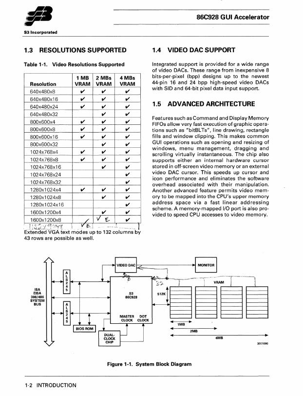
When used on the motherboard, the 86C928 can directly connect to the 386DX/486 CPU bus. A 386/486 no-wait-state memory read/write cycle is provided for this configuration, resulting in very high performance in a PC environment. The 86C928 also contains a 32-bit EISA interface for use with add-in board graphics subsystems. The 86C928 further integrates a 16-bit ISA bus interface for add-in board graphics subsystems. This interface supports no-wait-state ISA memory cycles. The accelerator's high level of integration facilitates low-chip-count implementations for all supported bus system configurations as shown by the system block diagram in Figure 1-1.
1.2 VRAM SUPPORT
The 86C928 accelerator contains a complete VRAM interface. Thus, it is ideal for the highest performance graphics systems. Display memory configurations of 0.5, 1, or 2 MBytes are supported without additional external logic, and 3 or 4 MByte configurations are supported with the addition of a simple decoder.
INTRODUCTION 1-1
•• r S3 Incorporated
1.3 RESOLUTIONS SUPPORTED
Table ,.,. Video Resolutions Supported
, MB 2 MBs 4MBs Resolution VRAM VRAM VRAM
640x480x8 v' v' v'
640x480x16 v' v' v'
640x480x24 v' v' v'
640x480x32 v' v'
800x600x4 v' v' v'
800x600x8 v' v' v'
800x600x16 v' v' v'
800x600x32 v' v'
1024x768x4 v' v' v'
1024x768x8 v' v' v'
1024x768x16 v' v'
1024x768x24 v'
1024x768x32 v'
1280x1024x4 v' v' v'
1280x1024x8 v' v'
1280x1024x16 v'
1600x1200x4 v' v'
1600x1200x8 / 'le- v'
~ ; ,~~;;:i __ ~:L?'I~rr \ .V~, I Extended VGA text modes up to 132 columns by 43 rows are possible as well.
ISA EISA
386/486 SYSTEM
BUS
A L
~ J--.----'-~ 4 5
A L
~~-+-r---~ 4 5
86C928 GUI Accelerator
1.4 VIDEO DAC SUPPORT
Integrated support is provided for a wide range of video DACs. These range from inexpensive 8 bits-per-pixel (bpp) designs up to the newest 44-pin 16 and 24 bpp high-speed video DACs with SID and 64-bit pixel data input support.
1.5 ADVANCED ARCHITECTURE
Features such as Command and Display Memory FIFOs allow very fast execution of graphic operations such as "bitBL Ts", line drawing, rectangle fills and window clipping. This makes common GUI operations such as opening and resizing of windows, menu management, dragging and scrolling virtually instantaneous. The chip also supports either an internal hardware cursor stored in off-screen video memory or an external video DAC cursor. This speeds up cursor and icon performance and eliminates the software overhead associated with their manipulation. Another advanced feature permits video memory to be mapped into the CPU's upper memory address space via a fast linear addressing scheme. A memory-mapped I/O port is also provided to speed CPU accesses to video memory.
.. ~ 1MB .. ~
2MB .. 4MB •
3001090
Figure ,.,. System Block Diagram
1-2 INTRODUCTION
86C928 GUI Accelerator
S3 Incorporated
Section 2: Pins
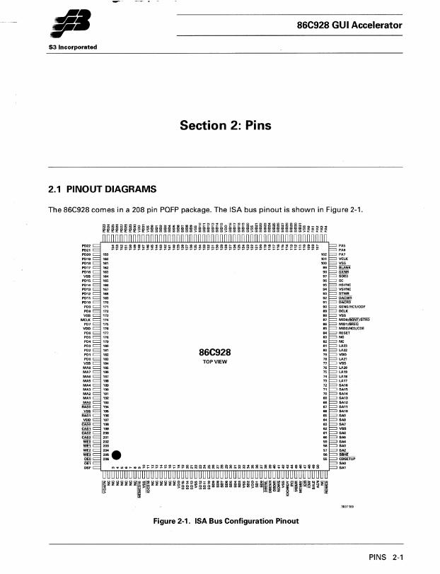
2.1 PINOUT DIAGRAMS
The 86C928 comes in a 208 pin PQFP package. The ISA bus pinout is shown in Figure 2-1.
P022 PD21 PO,. PD'B PD,B PD17 PD,. vss
PD15 PD14
PD" PD,. PD" PD,.
PD9 PD6 vss
MCLK POl
VDD PD6 PD5 PD4 PO> PD2 PD, POD vss MAO MAl MAO MAO MAC MAl MA2 MA, MAD
RASO vss
RAe, VDD
CA60 CAS' CAS' CA63 WED
WE' WE. WE. O£ij 0£1 os,
86C928 TOP VIEW
PAS PAS PAl VCLK vss BLANK SXNR SOED sc HSVNe ¥SYNC STWA OACWR DACRD SENS/HC1/0DF DCLK VSS M1DO/BGNT ISTRD MlD1/BREQ MlD2JHCO/CDE REseT NC NO LA23 LA22 YDO LA2, ¥SS LA20 LA,. LA18 LA17 SA'. SA,. SA14 SA" SA12 SA" SA10 SAO SAO SAl V58 SAO SAO SM SA3 SA> SBHE CDiETuji SAO
~TITnnTITnnTITnnTITnnTITnnnmnnnmTITnnTITnnTITnnTITnnTITnnTITnnTITnnnmmf--SA'
Figure 2-1. ISA Bus Configuration Pinout
PINS 2-1
•• r 86C928 GUI Accelerator
S3 Incorporated
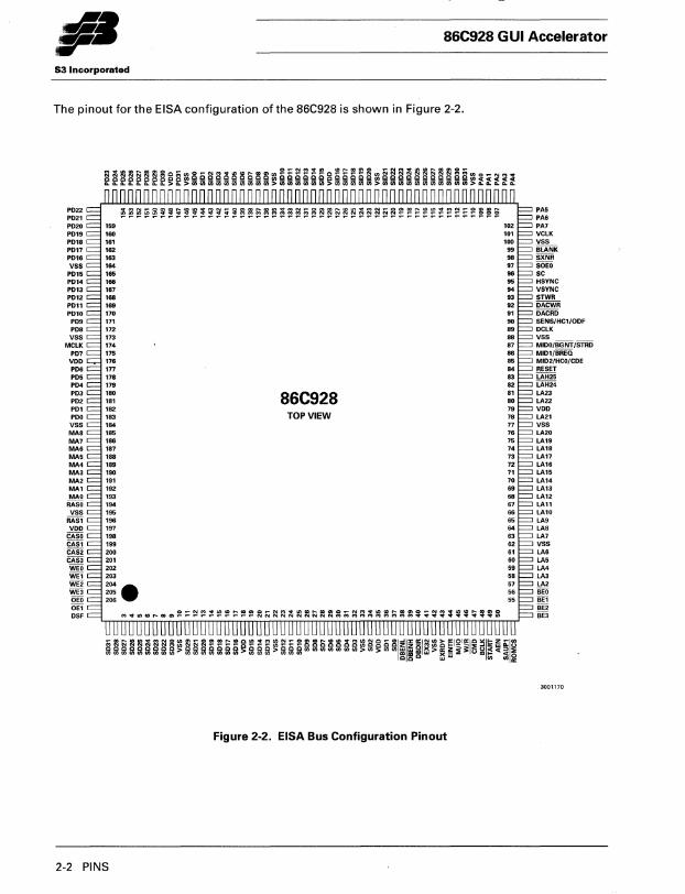
The pinout for the EISA configuration of the 86C928 is shown in Figure 2-2.
P022 PA5 P02, PAS P020 PA7 PD19 VClK POlS ~ P017 BLANK P016 SXNR VSS SOEO
P01S sc PD14 HSYNC P013 VSYNC P012 STWR P011 DACWR POlO DACRD PD. SENS/HC1/0DF PDS DCLK VSS VSS
MCLK MIDO/BGNT ISTRD PD7 MID1/BREQ VDD MID2/HCO/CDE PDS RESET PD5 LAH25 PD4 LAH24 PD. 86C928 LA2. PD2 LA22 PD1 VDD POD TOP VIEW LA21 vss VSS MAS LA20 MA7 LA1' MAS LA18 MA5 LA17 MAO LA16 MA. LA15 MA2 LA14 MA1 LA13 MAO LA12
RASO LA11 VSS LA10
HAS, LA. VDD LAS
CASO LA7 CAS' VSS CAS2 LAS CAsa LA5 WED LAO WE1 LA. WE2 LA2 WE. BED OED BE1 OE1 BE2 DSF BE.
3001170
Figure 2-2. EISA Bus Configuration Pinout
2-2 PINS
86C928 GUI Accelerator
S3 Incorporated
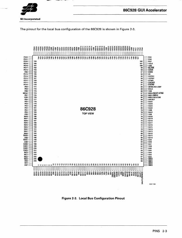
The pinout for the local bus configuration of the 86C928 is shown in Figure 2-3.
P022 PA5 P021 PAG P020 PA7 P019 VCLK P018 vss P017 BLANK P016 SXNR VSS SOEO
P015 sc P014 HSVNC P013 VSVNC PD12 STWA POll DACWR POlO DACRO
PD. SENS/HC1/0DF PDS DctK VSS VSS
MCLK MIDO/BGNT ISTRD PD7 MID1/BREQ
VDD MI02/HCO/CDE PDG SRESET PD5 SA25 PD4 SA24 PO, SA2' PD2 86C928 SA22 PO, VDD PDO
TOP VIEW SA2l
vss VSS MAS SA20 MA7 SA19 MAG SA1S MA5 SA17 MA4 $A16 MA3 SA1S MA2 SA14 MA' SAll MAO SA12
RASO SA11 VSS SA10
RASl SA. VDD SAS
CASO SA7 CASl VSS CAS2 SAG CAsa SA5 WEO SA4 WE' SAl WE2 SA2 WE' SBEO OEO SBEl OE, SBE2 DSF SBEl
Figure 2-3. Local Bus Configuration Pinout
PINS 2-3
86C928 GUI Accelerator
S3 Incorporated
2.2 PIN DESCRIPTIONS
The following table provides a brief description of each pin on the 86C928 for its ISA, EISA and local bus configurations. The following definitions are used in these descriptions;
I - Input signal 0- Output signal B - Bidirectional signal
Some pins have multiple names. This reflects the different functions performed by those pins depending on the bus configuration selected by power-on-strapping. The pin definitions and functions are given for each possible case.
Table 2-1. 86C928 Pin Descriptions
Symbol Type Pin Numberls) Description
BUS INTERFACES
Address and Data ----_ ..
SD[15:0] B 19-21, 23-32, System Data Bus. (lSA) SD[7:0] also serve as the 34,36,37 Video DAC Data Bus and as the General Input Port
Data Bus. SD[11 :8] act as the video DAC register select bits as well.
SD[310] 1, 9, 11, 2-8, System Data Bus. (EISA and Local Bus) SD[7:0] also 12-17,19-21, serve as the Video DAC Data Bus and as the General 23-32, 34, 36, Input Port Data Bus. SD[11 :8] act as the video DAC 37 register select bits as well.
LA[23:17] I 81-80, 78, Unlatched Address Bits. (ISA) 76-73
LAH[25:24] 83,82 System Upper Address Bits. (EISA)
SA[2524] System Address Bus Bits. (Local Bus)
SA[15:0] I 71-63, 61-57, System Address Bus. (ISA) 53, 54
LA[23:2] 81, 80, 78, 76- System Address Bus. (EISA) 63,61-57
SA[232] System Address Bus. (Local Bus)
SBHE I 56 High Data Byte Enable. (lSA)
---BE[3:0] 53-56 Data Byte Enables. (EISA)
---SBE[3:0] Data Byte Enables. (Local Bus)
SAUP1 I 51 Upper Address Decode. (EISA)
SAUP[21] 52, 51 Upper Address Decodes. (Local Bus) SAUP2 also serves as a BIOS ROM Chip Select output
2-4 PINS
86C928 GUI Accelerator
S3 Incorporated
Table 2-1. 86C928 Pin Descriptions (Continued)
Symbol Type Pin Number(s) Description Bus Control
AEN I 50 Address Enable. (lSA, EISA) When asserted, this signal allows DMA transfers to occur.
--RDYIN Local Bus Cycle End Acknowledge. (Local Bus) The
86C805 holds read data valid on the bus until this input is asserted.
lOW I 48 I/O Write. (lSA)
BCLK Bus Clock. (EISA)
SCLK System Clock. (Local Bus)
lOR I 47 I/O Read. (ISA)
--CMD Bus Cycle Timing Control. (EISA)
-SD/C Data/Control Cycle Indicator. (Local Bus)
IRQ 0 44 Interrupt Request. (lSA)
EINTR Interrupt Request. (EISA)
SINTR Interrupt Request. (Local Bus)
ENEID 0 52 EISA ID. This signal is externally decoded using M/IO. It is valid during I/O cycles. This pin can also serve as the BIOS ROM chip select (ROMCS) during memory cycles. (EISA)
SAUP2 I Upper Address Decode Bit 2. Also serves as a BIOS ROM Chip Select output (ROMCS) (Local Bus)
10CHRDY 0 43 Channel Ready. (lSA)
EXRDY Wait State Request. (EISA)
--SRDY Local Bus Cycle End. (Local Bus)
NOWS 0 41 Zero Wait-State Cycle. (lSA)
--EX32 32-bit Slave Indicator. (EISA)
--LOCA Local Bus Access Cycle Indicator. (Local Bus)
MEMR I 45 Memory Read. (lSA)
-M/IO Memory/IO Cycle Indicator. (EISA)
-SM/IO Memory/IO Cycle Indicator. (Local Bus)
RESET I 84 Reset. (lSA, EISA)
SRESET System Reset. (Local Bus)
PINS 2-5
•• r 86C928 GUI Accelerator
S3 Incorporated
Table 2-1. 86C928 Pin Descriptions (Continued)
Symbol Type Pin Number(s) Description
BALE I 49 Buffer Address Latch Enable. (ISA)
START Cycle Start Strobe. (EISA)
--SADS System Address Strobe. (Local Bus)
MEMW I 46 Memory Write. (lSA)
-W/R Write/Read Cycle Indicator. (EISA)
-SW/R Write/Read Cycle Indicator. (Local Bus)
CDSETUP I 55 Card Setup. (lSA)
VGAEN I 1 Enable VGA I/O and memory access. (ISA)
MEMCS16 0 9 Memory 16-bit Access. (ISA)
IOCS16 0 11 I/O 16-bit Access. (lSA)
External Buffer and EPROM Control
DBDIR 0 40 Data Buffer Direction Control. This signal is high for a data write and low for a data read.
DBENH 0 39 Data Buffer High-Byte Enable. This active low signal enables extemal data buffers for data bits SD[31 :8].
DBENL 0 38 Data Buffer Low-Byte Enable. This active low signal enables an external data buffer for data bits SD[7:0).
ROMCS 0 52 BIOS ROM Chip Select. Also can serve as the local bus ~address decode bit 2 (SAUP2) or the EISA bus ENEID signal.
CLOCK CONTROL
MCLK I 174 Master (Memory) Clock
DCLK I 89 Dot Clock. This input is provided bv the clock chip.
STWR 0 93 Clock Select Strobe. Also serves as the General Output Port Write Strobe.
PA[3:0] 0 106-109 Clock Select Bits. Also serve as pixel address bits to the video DAC.
DISPLAY MEMORY INTERFACE
Address and Data PD[31 :0] B 147.149-163, Pixel Data Bus. PDf 15-0] are also used as the system
165-172,175, configuration strapping bits, providing system 177-183 configuration and setup information upon power-on or
reset.
SID[31:0] I 111-121,123- Serial Input Pixel Data Bus. 127,129-134, 136-145
MA[8:0] 0 185-193 Memory Address Bus.
2-6 PINS
86C928 GUI Accelerator
53 Incorporated
Table 2-1. 86C928 Pin Descriptions (Continued)
Symbol Type Pin Number(s) Description Memory Control
RAS[1:0] 0 196,194 Row Address Strobes for each 1 MByte memory bank.
CAS[3:0] 0 201-198 Column Address Strobes for each pixel data byte.
WE[3:0] 0 205-202 Write Enables for upper and lower pixel data nibbles.
OE[1:0] 0 207-206 Output Enables for each 2 MByte memory bank.
SO EO 0 97 Serial Pixel Select for the 1 st MByte memory bank for configurations up to 2 MBytes. Externally decoded with SXNR to produce serial pixel selects for each MByte bank in configurations from 2 to 4 MBytes.
SXNR 0 98 Serial Pixel Select for the 2nd MByte memory bank for configurations up to 2 MBytes. Externally decoded with SO EO to produce serial pixel selects for each MByte bank in configurations from 2 to 4 MBytes.
SC 0 96 Serial Pixel Data Clock.
DSF 0 208 Special VRAM Function Control.
VIDEO DAC INTERFACE
Address and Data
PA[7:0] 0 102-109 Video DAC Pixel Address Bus. These signals also serve as the General Output Port Data Bus. PA[3:0] also serve as the Clock Select Bits.
SD[7:0] B 28-32, 34, 36, Video DAC Data Bus. These signals also serve as the 37 System Data Bus bits and as the General Input Port
Data bus.
SD[11 :8] B 24-27 Video DAC Register Select. These signals also serve as System Data Bus bits.
Video DAC Control
VCLK 0 101 Video/Pixel Clock
DACRD 0 91 Video DAC Read. This active low signal, when asserted, indicates a data read from the video DAC.
DACWR 0 92 Video DAC Write. This active low signal, when asserted, indicates a data write to the video DAC.
BLANK 0 99 Video Blank. Asserting this active low signal turns off the video output.
SENS I 90 Video Level Sense. The video DAC asserts this active high signal when it detects the appropriate video voltage on the analog outputs. When bit 5 of the Extended DAC Control register (3?5H, Index 55H) is set to 1, this signal becomes the HC1 signal. If bit 5 of the Hardware Graphics Cursor Mode register (3?5H, Index 45H) is then set to 1, this becomes the ODF signal.
HSYNC 0 95 Horizontal Sync.
VSYNC B 94 Vertical Sync.This is an input for genlock support.
PINS 2-7
fl· 86C928 GUI Accelerator
S3 Incorporated
Table 2-1. 86C928 Pin Descriptions (Continued)
Symbol Type Pin Number(s) Description
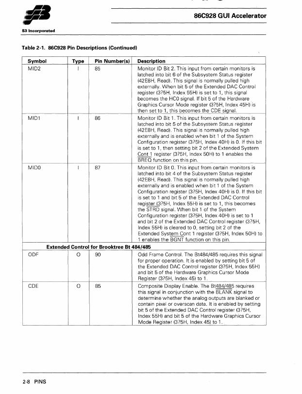
MID2 I 85 Monitor ID Bit 2. This input from certain monitors is latched into bit 6 of the Subsystem Status register (42E8H, Read). This signal is normally pulled high externally. When bit 5 of the Extended DAC Control register (3?5H, Index 55H) is set to 1, this signal becomes the HCO signal. If bit 5 of the Hardware Graphics Cursor Mode register (3?5H, Index 45H) is then set to 1, this becomes the CDE signal.
MID1 I 86 Monitor ID Bit 1. This input from certain monitors is latched into bit 5 of the Subsystem Status register (42E8H, Read). This signal is normally pulled high externally and is enabled when bit 1 of the System Configuration register (3?5H, Index 40H) is O. If this bit is set to 1, then setting bit 2 of the Extended System Cont 1 register (3?5H, Index 50H) to 1 enables the BREQ function on this pin.
MIDO I 87 Monitor ID Bit O. This input from certain monitors is latched into bit 4 of the Subsystem Status register (42E8H, Read). This signal is normally pulled high externally and is enabled when bit 1 of the System Configuration register (3?5H, Index 40H) is O. If this bit is set to 1 and bit 5 of the Extended DAC Control register (3?5H, Index 55H) is set to 1, this becomes the STRD signal. When bit 1 of the System Configuration register (3?5H, Index 40H) is set to 1 and bit 2 of the Extended DAC Control register (3?5H, Index 55H) is cleared to 0, setting bit 2 of the Extended System Cont 1 register (3?5H, Index 50H) to 1 enables the BGNT function on this pin.
Extended Control for Brooktree Bt 484/485
ODF 0 90 Odd Frame Control. The Bt484/485 requires this signal for proper operation. It is enabled by setting bit 5 of the Extended DAC Control register (3?5H, Index 55H) and bit 5 of the Hardware Graphics Cursor Mode Register (3?5H, Index 45) to 1.
CDE 0 85 Composite Display Enable. The Bt484/485 requires this signal in conjunction with the BLANK signal to determine whether the analog outputs are blanked or contain pixel or overscan data. It is enabled by setting bit 5 of the Extended DAC Control register (3?5H, Index 55H) and bit 5 of the Hardware Graphics Cursor Mode Register (3?5H, Index 45) to 1.
2-8 PINS
86C928 GUI Accelerator
53 Incorporated
Table 2-1. 86C928 Pin Descriptions (Continued)
Symbol Type Pin Number(s) Description MISCELLANEOUS FUNCTIONS
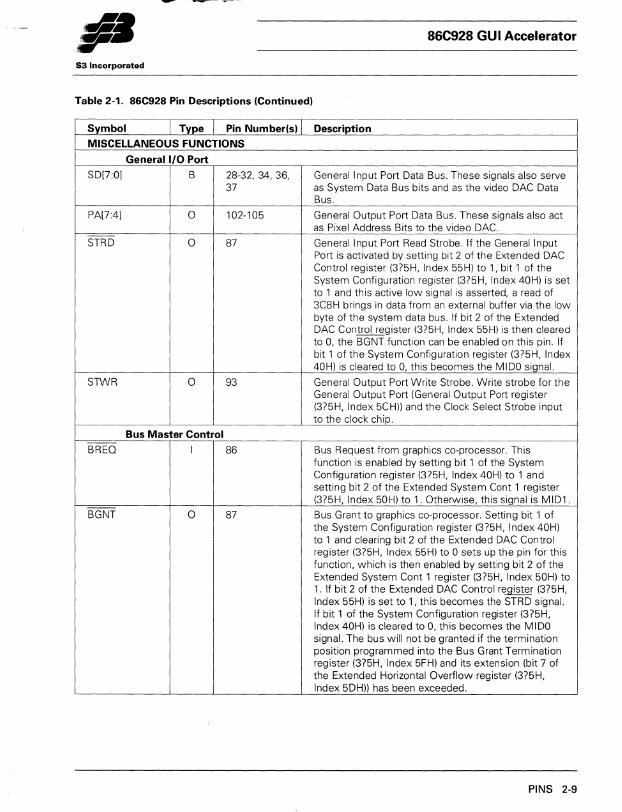
General 1/0 Port SD[7:0] B 28-32, 34, 36, General Input Port Data Bus. These signals also serve
37 as System Data Bus bits and as the video DAC Data Bus.
PA[7:4] 0 102-105 General Output Port Data Bus. These signals also act as Pixel Address Bits to the video DAC.
STRD 0 87 General Input Port Read Strobe. If the General Input Port is activated by setting bit 2 of the Extended DAC Control register (3 75H, Index 55H) to 1, bit 1 of the System Configuration register (3?5H, Index 40H) is set to 1 and this active low signal is asserted, a read of 3C8H brings in data from an external buffer via the low byte of the system data bus. If bit 2 of the Extended DAC Control register (3?5H, Index 55H) is then cleared to 0, the BGNT function can be enabled on th is pin. If bit 1 of the System Configuration register (375H, Index 40H) is cleared to 0, this becomes the MIDO signal.
STWR 0 93 General Output Port Write Strobe. Write strobe for the General Output Port (General Output Port register (3?5H, Index 5CH)) and the Clock Select Strobe input to the clock chip.
Bus Master Control BREQ I 86 Bus Request from graphics co-processor. This
function is enabled by setting bit 1 of the System Configuration register (3 75H, Index 40H) to 1 and setting bit 2 of the Extended System Cant 1 register (3?5H, Index 50H) to 1. Otherwise, this signal is MID1.
BGNT 0 87 Bus Grant to graphics co-processor. Setting bit 1 of the System Configuration register (3?5H, Index 40H) to 1 and clearing bit 2 of the Extended DAC Control register (3?5H, Index 55H) to 0 sets up the pin for this function, which is then enabled by setting bit 2 of the Extended System Cont 1 register (3?5H, Index 50H) to 1. If bit 2 of the Extended DAC Control register (3?5H, Index 55H) is set to 1, this becomes the STRD signal. If bit 1 of the System Configuration register (3?5H, Index 40H) is cleared to 0, this becomes the MIDO signal. The bus will not be granted if the termination position programmed into the Bus Grant Termination register (3?5H, Index 5FH) and its extension (bit 7 of the Extended Horizontal Overflow register (3?5H, Index 5DH)) has been exceeded.
PINS 2-9
fl· 86C928 GUI Accelerator
S3 Incorporated
Table 2-1. 86C928 Pin Descriptions (Continued)
Symbol Type Pin Number(s) Description
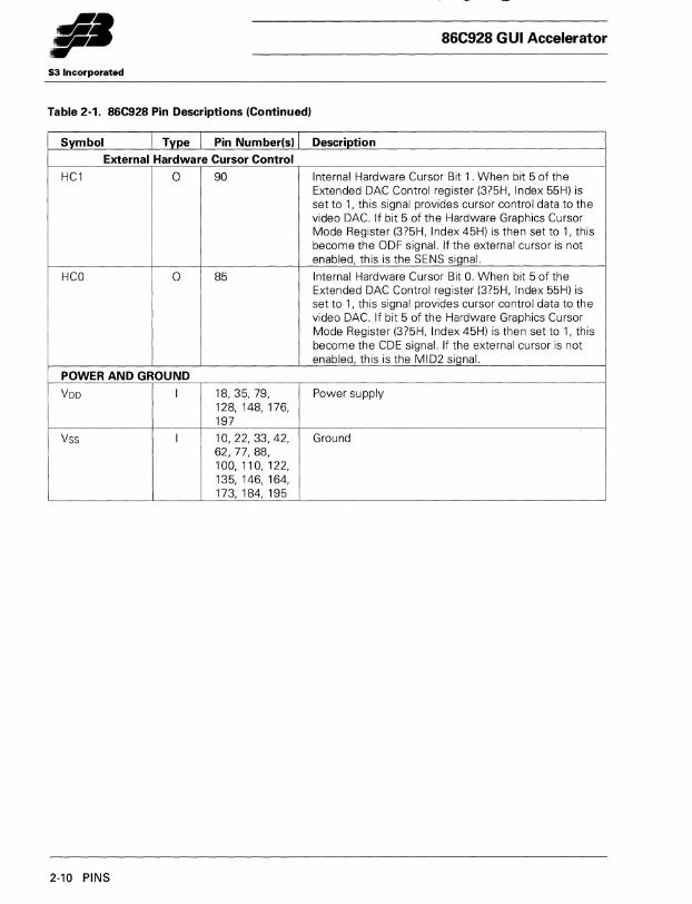
External Hardware Cursor Control
HC1 0 90 Internal Hardware Cursor Bit 1 . When bit 5 of the Extended DAC Control register (3?5H, Index 55H) is set to 1, this signal provides cursor control data to the video DAC. If bit 5 of the Hardware Graphics Cursor Mode Register (3?5H, Index 45H) is then set to 1, this become the ODF signal. If the external cursor is not enabled, this is the SENS signal.
HCO 0 85 Internal Hardware Cursor Bit O. When bit 5 of the Extended DAC Control register (3?5H, Index 55H) is set to 1, this signal provides cursor control data to the video DAC. If bit 5 of the Hardware Graphics Cursor Mode Register (3?5H, Index 45H) is then set to 1, this becorne the CDE signal. If the external cursor is not enabled, this is the MID2 signal.
POWER AND GROUND
VDD I 18,35, 79, Power supply 128,148,176, 197
Vss I 10,22,33,42, Ground 62,77,88, 100, 110, 122, 135,146,164, 173,184,195
2-10 PINS
•• r 86C928 GUI Accelerator
S3 Incorporated
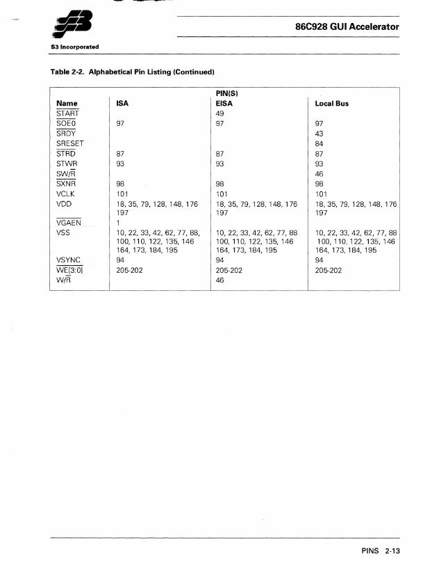
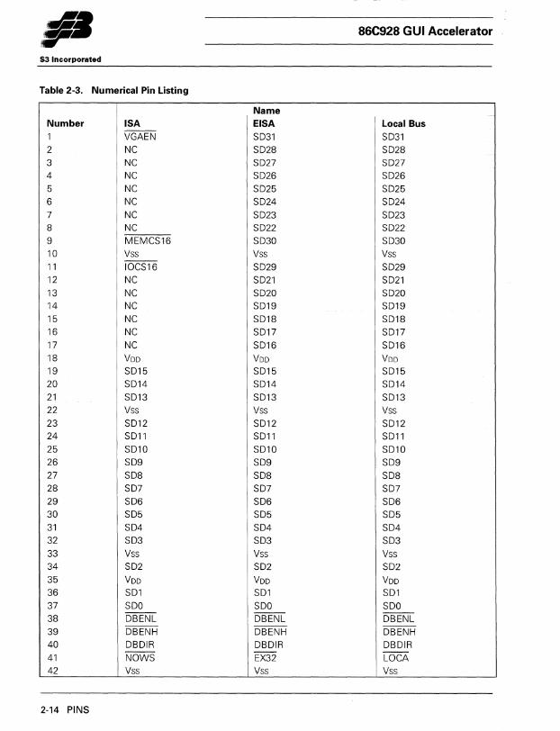
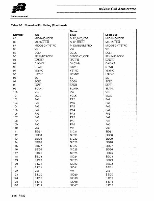
2.3 PIN LISTS
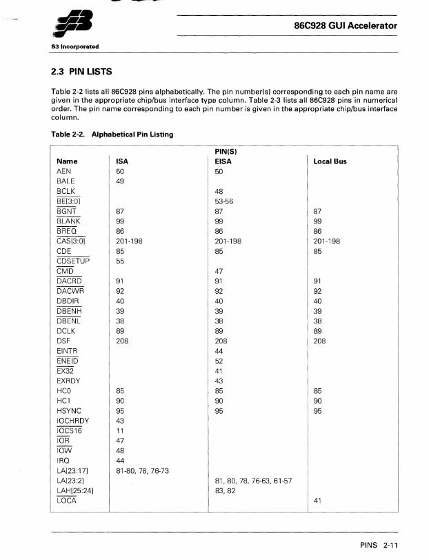
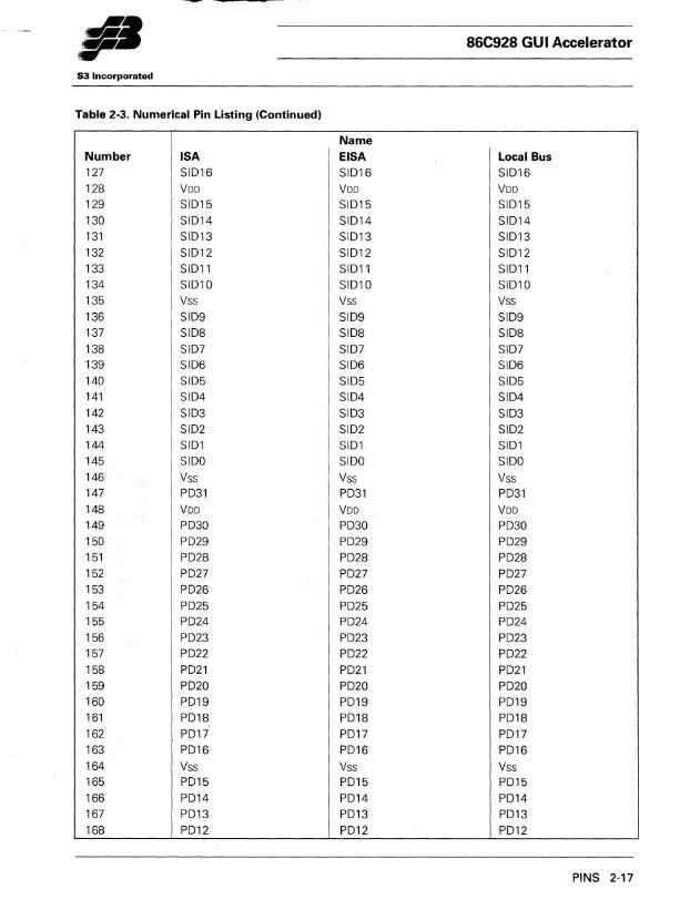
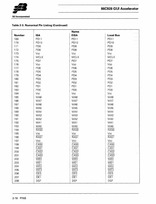
Table 2-2 lists all 86C928 pins alphabetically. The pin number(s) corresponding to each pin name are given in the appropriate chip/bus interface type column. Table 2-3 lists all 86C928 pins in numerical order. The pin name corresponding to each pin number is given in the appropriate chip/bus interface column.
Table 2-2. Alphabetical Pin Listing
Name AEN BALE
BCLK BE[3:0]
BGNT BLANK BREQ CAS[3:0]
CDE CDSETUP
CMD DACRD DACWR
DBDIR
DBENH DBENL DCLK DSF
EINTR ENEID
EX32 EXRDY
HCO HC1
HSYNC
ISA
50 49
87
99 86 201-198
85 55
91
92 40
39 38
89 208
85 90
95 10CHRDY 43 IOCS16 11 lOR 47
lOW 48 IRQ 44 LA[23:17] LA[23:2]
LAH[25:24]
LOCA
81-80, 78, 76-73
PIN(S)
EISA
50
48 53-56
87 99 86 201-198
85
47 91
92 40
39 38
89 208
44 52
41 43
85 90
95
81,80,78,76-63,61-57
83, 82
Local Bus
87 99 86 201-198
85
91
92 40
39 38
89 208
85 90
95
41
PINS 2-11
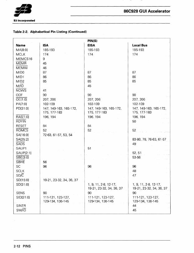
-~. r 53 Incorporated
Table 2-2. Alphabetical Pin Listing (Continued)
Name ISA MA[8:0J 185-193
MCLK 174 MEMCS16 9 MEMR 45
MEMW 46 MIDO 87
MID1 86 MID2 85
MilO NOWS 41
ODF 90 OE[1 :OJ 207, 206
PA[7:0J 102-109 PD[31:0J 147,149-163,165-172,
175,177-183
RAS[1 :OJ 196,194 RDYIN RESET 84 ROMCS 52 SA[16:0J 72-63,61-57,53,54
SA[25:2J
SADS SAUP1
SAUP[2:1J ---SBE[3:0J
SBHE 56 SC 96
SCLK SDic SD[15:0J 19-21,23-32,34,36,37 SD[31 :OJ
SENS 90 SID[31:0J 111-1 21, 1 23-1 27,
129-134, 136-145 SINTR
SM/IO
2-12 PINS
86C928 GUI Accelerator
PIN(S) EISA Local Bus 185-193 185-193 174 174
87 87
86 86 85 85
45
90 90 207, 206 207, 206 102-109 102-109 147,149-163,165-172, 147,149-163,165-172, 175,177-183 175,177-183
196. 194 196,194
50 84 52 52
83-80, 78, 76-63, 61-57
49 51
52,51 -
53-56
96 96 48 47
1,9,11,2-8,12-17, 1,9,11,2-8,12-17, 19-21,23-32,34,36,37 ... 19-21, 23-32, 34, 36, 37
90 90 111-1 21, 1 23-1 27, 111-121,123-127, 129-134, 136-145 129-134,136-145
44 45
86C928 GUI Accelerator
S3 Incorporated
Table 2-2. Alphabetical Pin Listing (Continued)
PIN(S) Name ISA EISA Local Bus START 49 SOEO 97 97 97 SRDY 43 SRESET 84 STRD 87 87 87 STWR 93 93 93 SWjR 46 SXNR 98 98 98 VCLK 101 101 101 VDD 18, 35, 79, 128, 148, 176 18,35,79,128,148,176 18,35,79, 128, 148, 176
197 197 197 VGAEN VSS 10,22,33,42,62,77,88, 10,22,33,42,62,77,88 10,22,33,42,62,77,88
100, 110, 122, 135, 146 100, 110, 122, 135, 146 100,110,122,135,146 164,173,184,195 164, 173, 184, 195 164,173,184,195
VSYNC 94 94 94 WE[3:0] 205-202 205-202 205-202 W/R 46
PINS 2-13
86C928 GUI Accelerator
53 Incorporated
Table 2-3. Numerical Pin Listing
Name Number ISA EISA Local Bus
--1 VGAEN S031 S031 2 NC S028 S028 3 NC S027 S027 4 NC S026 S026
5 NC S025 S025 6 NC S024 S024 7 NC S023 S023 8 NC S022 S022
9 MEMCS16 S030 S030 10 Vss Vss Vss 11 IOCS16 S029 S029 12 NC S021 S021 13 NC S020 S020 14 NC S019 S019
15 NC S018 S018 16 NC S017 S017 17 NC S016 S016 18 VDD VDD VDD 19 S015 S015 S015 20 S014 S014 S014 21 S013 S013 S013 22 Vss Vss Vss 23 S012 S012 S012 24 S011 S011 S011
25 S010 S010 S010 26 S09 S09 S09 27 S08 S08 S08 28 S07 S07 S07 29 S06 S06 S06 30 S05 S05 S05 31 S04 S04 S04 32 S03 S03 S03
33 Vss Vss Vss 34 S02 S02 S02 35 VDD VDD VDD 36 S01 S01 S01 37 SOO SOO SOO
-- -- --38 OBENL OBENL OBENL
--- --- ---39 OBENH OBENH OBENH 40 OBOIR OBOIR OBOIR -- -- --41 NOWS EX32 LOCA 42 Vss Vss Vss
2-14 PINS

.... r 53 Incorporated
Table 2-3. Numerical Pin Listing (Continued)
Number ISA 43 IOCHRDY 44 IRO
--45 MEMR 46 MEMW
-47 lOR --48 lOW 49 BALE 50 AEN 51 NC ---52 ROMCS 53 SA1 54 SAO 55 CDSETUP --56 SBHE 57 SA2 58 SA3 59 SA4 60 SA5 61 SA6 62 Vss 63 SA7 64 SA8 65 SA9 66 SA 10 67 SA11 68 SA12 69 SA13 70 SA14 71 SA15 72 SA16 73 LA17 74 LA18 75 LA19 76 LA20 77 Vss 78 LA21 79 Voo 80 LA22 81 LA23 82 NC 83 NC 84 RESET
86C928 GUI Accelerator
Name EISA Local Bus
EXRDY SRDY EINTR SINTR MilO SM/IO W/R SW/R -- -CMD SD/C BCLK SCLK --START SADS
--AEN RDYIN SAUP1 SAUP1 ----- ---ENEID/ROMCS SAUP2/ROMCS - --BE3 SBE3 - --BE2 SBE2 - --BE1 SBE1 BEO SBEO LA2 SA2 LA3 SA3 LA4 SA4 LA5 SA5 LA6 SA6 Vss Vss LA7 SA7 LA8 SA8 LA9 SA9 LA 10 SA 10 LA11 SA 11 LA12 SA12 LA13 SA13 LA14 SA14 LA15 SA15 LA16 SA16 LA17 SD17 LA18 SA18 LA19 SA19 LA20 SA20 Vss Vss LA21 SA21 VDD Voo LA22 SA22 LA23 SA23 --LAH24 SA24 --LAH25 SA25 RESET SRESET
PINS 2-15
fl· 86C928 GUI Accelerator
S3 Incorporated
Table 2-3. Numerical Pin Listing (Continued)
Name Number ISA EISA Local Bus 85 MID2/HCO/CDE MID2/HCO/CDE MID2/HCO/CDE -- -- --86 MID1/BREO MID1/BREO MID1/BREO
----87 MIDO/BGNT/STRD M IDO/BGNT/STRD MIDO/BGNT/STRD
88 Vss Vss Vss
89 DCLK DCLK DCLK
90 SENS/HC1/0DF SENS/HC1/0DF SENS/HC1/0DF --- --- ---
91 DACRD DACRD DACRD --- --- ---
92 DACWR DACWR DACWR
93 STWR STWR STWR
94 VSYNC VSYNC VSYNC
95 HSYNC HSYNC HSYNC
96 SC SC SC -- --
97 SOEO SOEO SOEO --98 SXNR SXNR SXNR
-- -- --99 BLANK BLANK BLANK
100 Vss Vss Vss
101 VCLK VCLK VCLK
102 PA7 PA7 PA7 -
103 PA6 PA6 PA6
104 PA5 PA5 PA5
105 PA4 PA4 PA4 --
106 PA3 PA3 PA3
107 PA2 PA2 PA2
108 PA1 PA1 PA1
109 PAO PAO PAO
110 Vss Vss Vss
111 SID31 SID31 SID31
112 SID30 SID30 SID30
113 SID29 SID29 SID29
114 SID28 SID28 SID28
115 SID27 SID27 SID27 --
116 SID26 SID26 SID26 ---
117 SID25 SID25 SID25 118 SID24 SID24 SID24
119 SID23 SID23 SID23
120 SID22 SID22 SID22
121 SID21 SID21 SID21
122 Vss Vss Vss
123 SID20 SID20 SID20
124 SID19 SID19 SID19
125 SID18 SID18 SID18
126 SID17 SID17 SID17
2-16 PINS
86C928 GUI Accelerator
53 Incorporated
Table 2·3. Numerical Pin Listing (Continued)
Name Number ISA EISA Local Bus 127 SI016 SI016 SI016 128 Voo Voo Voo 129 SI015 SI015 SI015 130 SI014 SI014 SI014 131 SI013 SI013 SI013 132 SI012 SI012 SI012 133 SIOll SIOll SIOll 134 SI010 SI010 SI010 135 Vss Vss Vss 136 SI09 SI09 SI09 137 SI08 SI08 SI08 138 SI07 SI07 SI07 139 SI06 SI06 SI06 140 SI05 SI05 SI05 141 SI04 SI04 SI04 142 SI03 SI03 SI03 143 SI02 SI02 SI02 144 SIOl SIOl SIOl 145 SIOO SIOO SIOO 146 Vss Vss Vss 147 P031 P031 P031 148 Voo Voo Voo 149 P030 P030 P030 150 P029 P029 P029 151 P028 P028 P028 152 P027 P027 P027 153 P026 P026 P026 154 P025 P025 P025 155 P024 P024 P024 156 P023 P023 P023 157 P022 P022 P022 158 P021 P021 P021 159 P020 P020 P020 160 P019 P019 P019 161 P018 P018 P018 162 P017 P017 P017 163 P016 P016 P016 164 Vss Vss Vss 165 P015 P015 P015 166 P014 P014 P014 167 P013 P013 . P013 168 P012 P012 P012
PINS 2·17
•• r 86C928 GUI Accelerator
S3 Incorporated
Table 2-3. Numerical Pin Listing (Continued)
Name Number ISA EISA Local Bus 169 POll POll POll
--
170 POlO POlO POlO 171 P09 P09 P09 172 P08 P08 P08
173 Vss Vss Vss 174 MCLK MCLK MCLK
175 P07 P07 P07 176 Voo Voo Voo 177 P06 P06 P06 178 P05 P05 P05
179 P04 P04 P04 180 P03 P03 P03 181 P02 P02 P02 182 POl POl POl
183 POO POO POO 184 Vss Vss Vss 185 MA8 MA8 MA8 186 MA7 MA7 MA7
187 MA6 MA6 MA6 188 MA5 MA5 MA5
189 MA4 MA4 MA4 190 MA3 MA3 MA3
191 MA2 MA2 MA2 192 MAl MAl MAl
193 MAO MAO MAO -- -- --
194 RASO RASO RASO
195 Vss Vss Vss 196 RASl RASl RASl 197 Voo Voo Voo 198 CASO CASO CASO
-- --199 CASl CASl CASl
-- --200 CAS2 CAS2 CAS2
-- --201 CAS3 CAS3 CAS3
-- -- --202 WEO WEO WEO
-- -- --203 WEl WEl WEl
-- -- --204 WE2 WE2 WE2
-- -- --205 WE3 WE3 WE3
- -206 OEO OEO OEO
- -207 OEl OEl OEl
208 OSF OSF OSF
2-18 PINS
86C928 GUI Accelerator
53 Incorporated
Section 3: Functional Description
This section describes the functional capabilities ofthe 86C928 that are beyond those provided by standard VGA controllers. Functions related to external hardware, such as video DAC and memory interfacing, are described in Section 12, Hardware Interface.
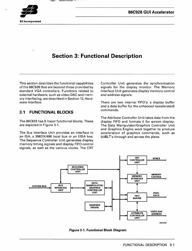
3.1 FUNCTIONAL BLOCKS
The 86C928 has 8 major functional blocks. These are depicted in Figure 3-1.
The Bus Interface Unit provides an interface to an ISA, a 386DX/486 local bus or an EISA bus. The Sequence Controller Unit generates display memory timing signals and display FIFO control signals, as well as the various clocks. The CRT
SYSTEM BUS
Controller Unit generates the synchronization signals for the display monitor. The Memory Interface Unit generates display memory control and address signals.
There are two internal FIFO's: a display buffer and a data buffer for the enhanced (accelerated) commands.
The Attribute Controller Unit takes data from the display FIFO and formats it for screen display. The Data Manipulator/Graphics Controller Unit and Graphics Engine work together to produce acceleration of graphics commands, such as bitBL T's through and across the plane.
SYNCS
MEMORY CONTROL
PIXEL DATA
VlDEODAC ADDRESS
3000640
Figure 3-1. Functional Block Diagram
FUNCTIONAL DESCRIPTION 3-'
S3 Incorporated
3.2 REGISTER ACCESS
In addition to all standard VGA and backward compatibility registers, the 86C928 contains several groups of registers providing advanced capabilities. These register groups must be unlocked before they can be accessed for reading or writing. This section explains how to unlock and relock each group.
Access to the S3 VGA Register group is gained by loading the bit pattern 01xx10xx (x = don't care) into Register Lock 1 (3?5H, Index 38H).
Access to the System Control and System Extension Register groups is gained by loading 101xxxxx into Register Lock 2 (3?5H, Index 39H).
Access to the Enhanced Graphic Command group is gained by setting bit 0 of the System Configuration register (3?5H, Index 40H) to 1. Note that the System Control Register group must be unlocked before this can be done.
Access to any register group can be re-Iocked by writing a bit pattern that changes any of the significant (non-don't care) bits.
3.3 VGA SETUP/ENABLE (lSA Only)
There are two standard methods of implementing VGA setup and configuration. One is the hardware method, where the VGAEN pin is strapped low to enable the video subsystem.
If VGAEN is strapped high, the software system setup method is used. Bit 4 of the Video Subsystem Access/Setup register (46E8H) is set to 1, bit o ofthe POS Mode Option Select register (102H) is set to 1 and then bit 3 of the 46E8H register is set to 1. This enables the video subsystem.
If bit 8 of configuration strapping (pin PD8) is 1, the 86C928 acts as a regular VGA for setup and bit 4 of the Video Subsystem Access/Setup register is used. If PD8 is set to 0, then bit 5 of the Video Subsystem Access/Setup register is used for setup.
3-2 FUNCTIONAL DESCRIPTION
86C928 GUI Accelerator
3.4 MODE AND CURSOR SETUPS
The 86C928 supports all standard VGA and VESA-compliant extended VGA modes. In addition, it offers enhanced (accelerated) modes beyond these standards. This section explains the setup methods for the various modes and the hardware cursor.
3.4.1 VGA Mode Setup
The 86C928 powers up into a standard VGA mode determined by the BIOS. The mode can then be altered by programming the standard VGA registers. All standard VGA modes are supported and the 86C928 remains in VGA mode until the Enhanced functions are enabled.
The 86C928 also supports the following extended VGA modes without providing hardware acceleration. The 4 bits/pixel modes operate just like the VGA planar modes and the 8 bits/pixel modes operate just like the VGA packed pixel modes.
• 640x480x8
• 800x600x4
• 800x600x8
• 1024x768x4
• 1024x768x8
See standard VESA-compliant documentation for the setup steps for these modes.
132 chl!racter text mode is supported. Bit 5 of the Miscellaneous 1 register (3?5H, Index 3AH) is set to one while loading the character fonts. It is then reset to o. Bit 6 of the Memory Configuration register (3?5H, Index 31H) is then set to 1 to enable the high speed text display font fetch (132 character) mode.
3.4.2 Backward Compatibility Modes Setup
The 86C928 is hardware compatible with CGA, MDA, and Hercules Graphics Card (HGC) standards which are based on the Motorola 6845 CRT controller. These standards are designed to run
•• r S3 Incorporated
on TTL (digital) monitors, however, the 86C928 uses analog displays for all modes. To emulate the 6845, the following additional setup is required before relinquishing control to 6845-based applications. This reconfiguration from VGA modes to corresponding CGA/MDA modes can be done with the aid of a BIOS call for 6845 emulation using INT 10. This procedure can be broken down into the following steps:
1. Character Generator Locking. The VGA BIOS reloads the character generator each time an alphanumeric mode is set whereas non-VGA modes (CGA, MDA, and Hercules) do not. Therefore the character table must be loaded onto plane 2 when the controller is still in the VGAmode.
2. Video DAC color compatibility. Non-VGA modes use 6-bit video output. Therefore, only the first 64 video DAC addresses need to be programmed and locked. Locking is done using bit 4 of the Backward Compatibility 2 register (3?5H, Index 33H).
3. Program default parameters. The 86C928 should be programmed for a 640 x 200 or 320 x 200 programming table for CGA, whereas MDA uses a 350-line programming table (Mode 7).
4. Set the S3 Registers for 6845 emulation by setting bit 3 of the Backward Compatibility 1 register (3?5H, Index 32H) to 1 to select nonVGA operation. Force high rate horizontal timing, then lock horizontal and vertical timing. These and other backward compatibility setup capabilities are provided by the Backward Compatibility 1 (3?5H, Index 32H), Backward Compatibility 2 (3?5H, Index 33H) and Backward Compatibility 3 (3?5H, Index 34H) registers.
At this point the 86C928 is hardware compatible with and can be programmed as a 6845. The program values will be inappropriate for VGA, but internal translation converts them to an equivalent value for analog monitors.
86C928 GUI Accelerator
3.4.3 Enhanced Mode Setup
Enhanced mode provides a number of video modes. These are listed in the Introduction ofthis data book.
After the desired mode is selected, the Enhanced Graphic Command group is unlocked by setting bit 0 of the System Configuration register (3?5H, Index 40H) to 1. After that, bit 0 of the Advanced Function Control register (4AE8H) must be set to 1 to enable Advanced Display functions.
Several advanced capabilities are available when in Enhanced mode. Their setups are described next.
Enhanced mode registers are located at I/O addresses x2E8H, x6E8H, xAE8H and xEE8H (x =
don't care). In order to prevent address conflicts with other I/O devices, they may be remapped to other I/O addresses by setting bit 4 of the Extended Mode register (3?5H, Index43H) to 1. The new address becomes the original address XORed with 3AOH, resulting in the following I/O addresses: x148H, x548H, x948H and xD48H. The Video Subsystem Access!Setup Enable Register (46E8H) is not affected by the setting of bit 4 of the Extended Mode register. All 16 bits ofthe I/O address are decoded.
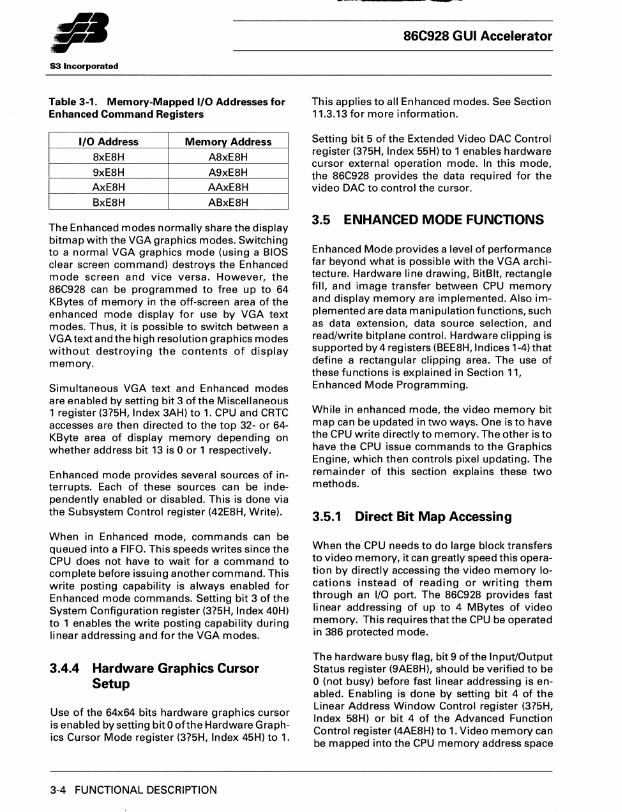
For improved performance, the Enhanced registers can be memory-mapped (MMIO). This function is enabled by setting bit 4 of the ~xtended Memory Control register (3?5H, Index 53H) or bit 5 of the Advanced Function Control register (4AE8H) to 1. Image transfers normally made by accessing I/O addresses E2E8H and E2EAH (the Pixel Data Transfer registers) are made instead by accessing any memory location in the 32-KByte address space from AOOOOH to A7FFFH. Accesses to the Enhanced command registers (write only) are made to particular locations in the A8000H to AFFFFH address range as shown in Table 3-1. The only exception is the Read Register Select register (BEE8H, Index OFH), which cannot be accessed as a memory-mapped register.
FUNCTIONAL DESCRIPTION 3-3
•.. fa ,.-S3 Incorporated
Table 3-1. Memory-Mapped I/O Addresses for Enhanced Command Registers
I/O Address Memory Address
8xE8H A8xE8H
9xE8H A9xE8H AxE8H AAxE8H BxE8H ABxE8H
The Enhanced modes normally share the display bitmap with the VGA graphics modes. Switching to a normal VGA graphics mode (using a BIOS clear screen command) destroys the Enhanced mode screen and vice versa. However, the 86C928 can be programmed to free up to 64 KBytes of memory in the off-screen area of the enhanced mode display for use by VGA text modes. Thus, it is possible to switch between a VGA text and the high resolution graphics modes without destroying the contents of display memory.
Simultaneous VGA text and Enhanced modes are enabled by setting bit 3 of the Miscellaneous 1 register (3?5H, Index 3AH) to 1. CPU and CRTC accesses are then directed to the top 32- or 64-KByte area of display memory depending on whether address bit 13 is 0 or 1 respectively.
Enhanced mode provides several sources of interrupts. Each of these sources can be independently enabled or disabled. This is done via the Subsystem Control register (42E8H, Write).
When in Enhanced mode, commands can be queue~ into a FIFO. This speeds writes since the CPU does not have to wait for a command to complete before issuing another command. This write posting capability is always enabled for Enhanced mode commands. Setting bit 3 of the System Configuration register (3?5H, Index40H) to 1 enables the write posting capability during linear addressing and for the VGA modes.
3.4.4 Hardware Graphics Cursor Setup
Use of the 64x64 bits hardware graphics cursor is enabled by setting bit 0 ofthe Hardware Graphics Cursor Mode register (3?5H, Index 45H) to 1.
3-4 FUNCTIONAL DESCRIPTION
86C928 GUI Accelerator
This applies to all Enhanced modes. See Section 11.3.13 for more information.
Setting bit 5 of the Extended Video DAC Control register (3?5H, Index 55H) to 1 enables hardware cursor external operation mode. In this mode, the 86C928 provides the data required for the video DAC to control the cursor.
3.5 ENHANCED MODE FUNCTIONS
Enhanced Mode provides a level of performance far beyond what is possible with the VGA architecture. Hardware line drawing, BitBlt, rectangle fill, and image transfer between CPU memory and display memory are implemented. Also implemented are data manipulation functions, such as data extension, data source selection, and read/write bitplane control. Hardware clipping is supported by 4 registers (BEE8H, Indices 1-4) that define a rectangular clipping area. The use of these functions is explained in Section 11, Enhanced Mode Programming.
While in enhanced mode, the video memory bit map can be updated in two ways. One is to have the CPU write directly to memory. The other is to have the CPU issue commands to the Graphics Engine, which then controls pixel updating. The remainder of this section explains these two methods.
3.5.1 Direct Bit Map Accessing
When the CPU needs to do large block transfers to video memory, it can greatly speed this operation by directly accessing the video memory locations instead of reading or writing them through an I/O port. The 86C928 provides fast linear addressing of up to 4 MBytes of video memory. This requires that the CPU be operated in 386 protected mode.
The hardware busy flag, bit 9 ofthe Input/Output Status register (9AE8H), should be verified to be o (not busy) before fast linear addressing is enabled. Enabling is done by setting bit 4 of the Linear Address Window Control register (3?5H, Index 58H) or bit 4 of the Advanced Function Control register (4AE8H) to 1. Video memory can be mapped into the CPU memory address space
•• r 53 Incorporated
using the Linear Address Window Control (3?5H, Index 58H) and the Linear Address Window Position (3?5H, Index 59H and 5AH) registers.
The access window into memory can be restricted to 64 KBytes, allowing use of real mode. This is enabled by setting bit 3 of the Memory Configuration register (3?5H, Index 31 H) to 1. A base address offset into display memory is then written into bits [3:0] of the CRT Register Lock register (3?5H, Index 35H) and into bits 2 and 3 of the Extended System Control 2 register (3?5H, Index 51 H). (These latter extension bits enable access to up to 4 MBytes of video memory.) The offset is then added to the memory address if bit ° of the Memory Configuration register (3?5H, Index 31H) is set to 1.
Direct bitmap accessing should not be enabled concurrently with memory-mapped I/O.
Bit 3 of the Memory Configuration register determines how the CPU memory access is translated into the display memory address. Ifthis bit is set to 1, linear mapping is used. If it is set to 0, VGA mapping is used. VGA mapping depends on the VGA mode, which is still set even though the 86C928 is in Enhanced mode.
3.5.2 Read-Ahead Cache
The read-ahead cache function is enabled by setting bit 2 ofthe Linear Address Window Control (3?5H, Index 58H) register to 1. Th is causes extra data to be pre-fetched during video memory reads and cached. Subsequent reads of data in the cache (a cache hit) return data immediately. This function applies to linear addressing reads and VGA memory reads.
The amount of pre-fetch data returned is determined by the setting of bits 2-0 of the Extended Memory Control 2 (3?5H, Index 54H) register. The meaningful values are 1, 3 and 7 so that prefetched data is restricted to a full address boundary. The number represents the extra doublewords to be pre-fetched for linear addressing and VGA doubleword modes. It specifies the number of extra words to be pre-fetched for VGA word modes and the number of extra bytes to be pre-fetched for VGA byte modes.
86C928 GUI Accelerator
Cache coherency is maintained through invalidation.
3.5.3 Bitmap Access Through the Graphics Engine
When updating pixels through the Graphics Engine, all CPU data moves through the Pixel Data Transfer register (E2E8H) for 16-bit transfers. This 16-bit register can be memory mapped as explained in section 3.4.3. The Pixel Data Transfer - Extension register (E2EAH) is also used for 32-bit transfers.
Each pixel is assigned a color index or true color value, which is translated via a programmable DAC before being displayed on a CRT. In addition, selected pixels can be masked off from being displayed by programming the DAC Mask register (03C6H).
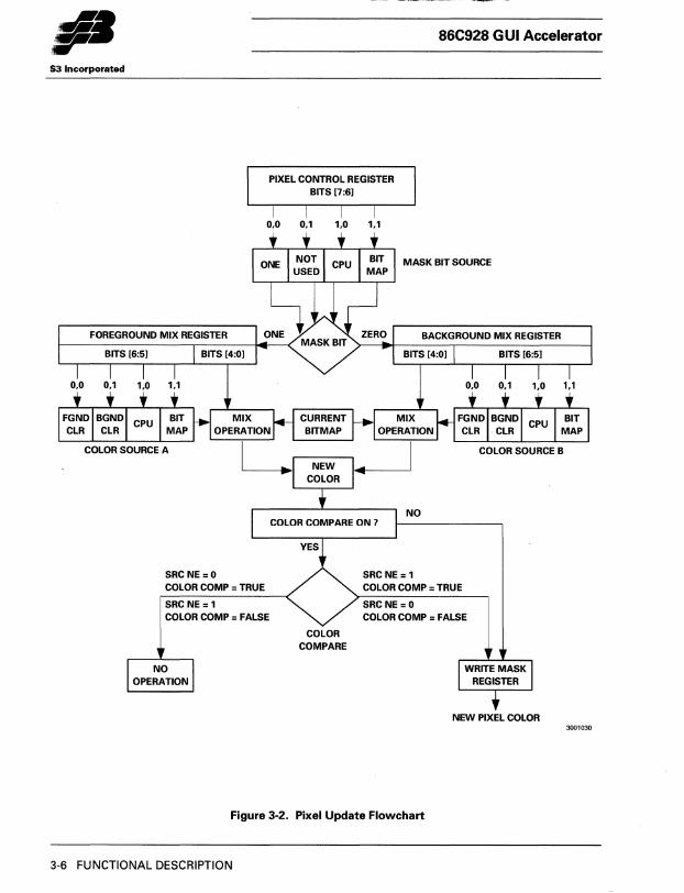
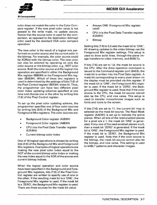
Figure 3-2 is a flowchart for the process of updating the color of each pixel. The remainder ofthis section explains this flowchart.
Start at the block labeled 'New Color' in the middle of Figure 3-2. At this stage, a color has been determined that mayor may not be used to update a pixel in the bitmap. How this color is determined will be covered later.
The first hurdle for the new color is the color compare process. If this is turned off (bit 8 ofthe Multifunction Control Miscellaneous (BEE8H, Index OEH) register = 0)' the new color is passed to the Write Mask register (AAE8H). If the plane to which the pixel update is directed has been masked off in this register, no update occurs. Otherwise, the new color is written to the bitmap.
Ifcolorcompare is enabled (bit 8 ofthe Multifunction Control Miscellaneous register = 1), the new color (source) is compared to a color programmed into the Color Compare (B2E8H) register. The sense of the color comparison is determined by the SRC NE (source not equal) bit (bit7) ofthe Multifunction Control Miscellaneous register. If this bit is 0, the new pixel color value is passed to the write mask only when the source color matches the color in the Color Compare register. If this bit is 1, the new pixel color value is passed to the write mask only when the source
FUNCTIONAL DESCRIPTION 3-5
53 Incorporated
0,0 0,1
86C928 GUI Accelerator
0,0 0,1 1,0 1.1
1,0 1,1
SRCNE=O COLOR COMP = TRUE
SRCNE=1 COLOR COMP = FALSE
COLOR COMPARE
MASK BIT SOURCE
0,0 0,1 1,0 1,1
COLOR COMP = TRUE
COLOR COMP = FALSE
NEW PIXEL COLOR 3001030
Figure 3-2. Pixel Update Flowchart
3-6 FUNCTIONAL DESCRIPTION
II· S3 Incorporated
color does not match the color in the Color Compare register. If the new pixel color value is not passed to the write mask, no update occurs. Notice that the sou rce color is used for the comparison, as opposed to the destination (bitmap) color used by the standard VGA color compare operation.
The new color is the result of a logical mix performed on a color source and the current color in the bitmap. For example, the color source could be XORed with the bitmap color. The new color can also be selected by operating on only the color source or the bitmap color, e.g., NOT color source. Both the color source and the logical mix operation are specified in either the Background Mix register (B6E8H) or the Foreground Mix register (BAE8H). Which of these two registers is used is determined by the settings of bits [7:6] of the Pixel Control register (BEE8H, Index A). Thus, the programmer can have two different pixel color index updating schemes specified at one time and choose one or the other by writing bits [7:6] of the Pixel Control register.
To set up the pixel color updating scheme, the programmer specifies one of four color sources by writing bits [6:5] of the Background Mix and Foreground Mix registers. The color sources are:
• Background Color register (A2E8H)
• Foreground Color register (A6E8H)
• CPU (via the Pixel Data Transfer register (E2E8H))
Current bitmap color index
One of 16 logical operations is chosen by writing bits [4:0] ofthe Background Mix and Foreground Mix registers. Examples of logical operations are making the new pixel color index equal to the NOT of the current bitmap color index or making the new index equal to the XOR of the source and current bitmap indices.
When the logical operation and color source have been specified in the Background and Foreground Mix registers, bits [7:6] of the Pixel Control register are written to specify use of one or the other. Ifthe resulting mask bit is a 'ONE', the Foreground Mix register is used. If the mask bit is a 'ZERO', the Background Mix register is used. There are three sources for the mask bit value:
•
•
86C928 GUI Accelerator
Always ONE (Foreground Mix register used)
CPU (via the Pixel Data Transfer register (E2E8H))
Bitmap
Setting bits [7:6] to 0,0 sets the mask bit to 'ONE'. All drawing updates to the video bitmap use the Foreground Mix register settings. This setup is used to draw solid lines, through-the-plane image transfers to video memory, and BitBLTs.
If bits [7:6] are set to 1,0, the mask bit source is the CPU. After the draw operation command is issued to the Command register port (9AE8), the mask bit is written into the Pixel Data register. A mask bit corresponding to every pixel drawn on the display must be provided via this register. If the mask bit is 'ONE', the Foreground Mix register is used. If the mask bit is 'ZERO', the Background Mix register is used. Note that ifthe color source is the CPU, the mask bit source cannot also be the CPU, and vice versa. This setup is used to transfer monochrome images such as fonts and icons to the screen.
If bits [7:6] are set to 11, the current bit map is selected as the mask bit source. The Read Mask register (AAE8H) is set up to indicate the active planes. When all bits of the read-enabled planes for a pixel are a 1, the mask bit 'ONE' is generated. If anyone ofthe read-enabled planes is a 0, then a mask bit 'ZERO' is generated. If the mask bit is 'ONE', the Foreground Mix register is used. If the mask bit is 'ZERO', the Background Mix register is used. Note that if the color source is the bitmap, the mask bit source cannot also be the bitmap, and vice versa. This setting is used to bitBL T patterns and character images.
FUNCTIONAL DESCRIPTION 3-7

86C928 GUI Accelerator
53 Incorporated
-----.~----------
86C928 GUI Accelerator
53 Incorporated
Section 4: CGA-Compatible Register Descriptions
In the following register descriptions, "U" stands for undefined or unused and "R" stands for reserved (write = 0, read = U).
See Appendix A for a table listing each register in this section and its page number.
Light Pen High Register (LPENH)
Read Only Address: 3D5H, Index 10H Power-On Default: Undefined
Light Pen Low Register (LPENL)
Read Only Address: 3D5H, Index 11 H Power-On Default: Undefined
7 6 5 4 3 2 o Light Pen Strobe Address Low
These registers contain the 14 memory address bits at the timethe light pen strobe signal was detected in CGA and HGC modes.
These registers are not available in VGA mode.
The light pen is not actually connected to most systems, but the LP set/reset flag can be used to read the video memory addresses at the vertical retrace interval. The CPU can read the video memory address through this register. The screen mode and the video memory address have a known ratio at· the vertical retrace interval. Therefore, the CPU can guess the screen mode (ex: low or high resolution, and text or graphics) from the light pen detect address at the vertical retrace.
The mode register is a write-only register, except in VGA mode. The CPU cannot read any screen mode information directly. Therefore the light pen detect address at the vertical retrace interval is used as a mode indicator indirectly in CGA and HGC modes.
CGA-COMPATIBLE REGISTER DESCRIPTIONS 4-1
S3 Incorporated
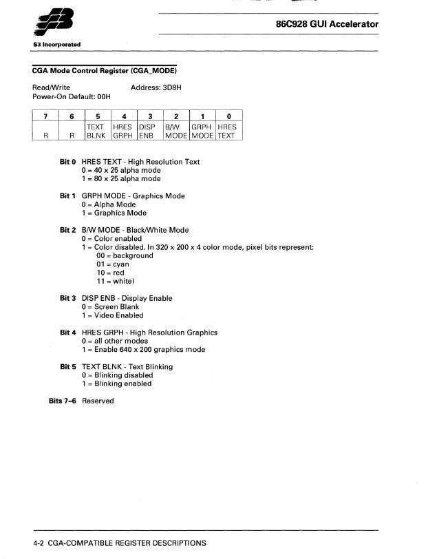
CGA Mode Control Register (CGA_MODE)
Read/Write Address: 3D8H Power-On Default: OOH
7 6 5 4 3 2 1
TEXT HRES DISP B/W GRPH R R BLNK GRPH ENB MODE MODE
Bit 0 HRES TEXT - High Resolution Text 0= 40 x 25 alpha mode 1 = 80 x 25 alpha mode
Bit 1 GRPH MODE - Graphics Mode 0= Alpha Mode 1 = Graphics Mode
Bit 2 B/W MODE - Black/White Mode o = Color enabled
86C928 GUI Accelerator
0
HRES TEXT
1 = Color disabled. In 320 x 200 x 4 color mode, pixel bits represent: 00 = background 01 = cyan 10 = red 11 = white)
Bit 3 DISP ENB - Display Enable o = Screen Blank 1 = Video Enabled
Bit 4 HRES GRPH - High Resolution Graphics 0= all other modes 1 = Enable 640 x 200 graphics mode
Bit 5 TEXT BLNK - Text Blinking 0= Blinking disabled 1 = Blinking enabled
Bits 7-6 Reserved
4-2 CGA-COMPATIBLE REGISTER DESCRIPTIONS
86C928 GUI Accelerator
S3 Incorporated
CGA Color Select Register (CGA_COLOR)
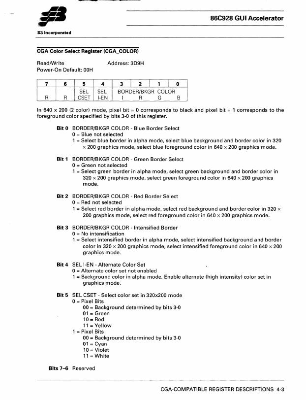
ReadIWrite Address: 3D9H Power-On Default: OOH
7 6 5 4 3 I 2 j 1 1 0
SEL SEL BORDER/BKGR COLOR R R CSET I-EN I R G B
In 640 x 200 (2 color) mode, pixel bit = 0 corresponds to black and pixel bit = 1 corresponds to the foreground color specified by bits 3-0 of this register.
Bit 0 BORDER/BKGR COLOR - Blue Border Select o = Blue not selected 1 = Select blue border in alpha mode, select blue background and border color in 320
x 200 graphics mode, select blue foreground color in 640 x 200 graphics mode.
Bit 1 BORDER/BKGR COLOR - Green Border Select o = Green not selected 1 = Select green border in alpha mode, select green background and border color in
320 x 200 graphics mode, select green foreground color in 640 x 200 graphics mode.
Bit 2 BORDER/BKGR COLOR - Red Border Select o = Red not selected 1 = Select red border in alpha mode, select red background and border color in 320 x
200 graphics mode, select red foreground color in 640 x 200 graphics mode.
Bit 3 BORDER/BKGR COLOR - Intensified Border o = No intensification 1 = Select intensified border in alpha mode, select intensified background and border
color in 320 x 200 graphics mode, select intensified foreground color in 640 x 200 graphics mode.
Bit 4 SEL I-EN - Alternate Color Set o = Alternate color set not enabled 1 = Background color in alpha mode. Enable alternate (high intensity) color set in
graphics mode.
Bit 5 SEL CSET - Select color set in 320x200 mode o = Pixel Bits
00 = Background determined by bits 3-0 01 = Green 10 = Red 11 = Yellow
1 = Pixel Bits 00 = Background determined by bits 3-0 01 = Cyan 10 = Violet 11 = White
Bits 7-6 Reserved
CGA-COMPATIBLE REGISTER DESCRIPTIONS 4-3
fl· 53 Incorporated
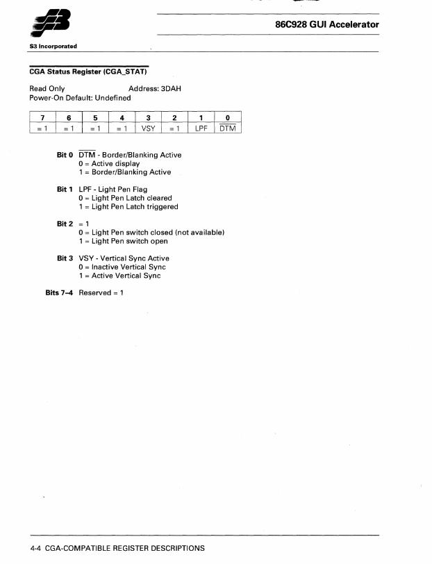
eGA Status Register (eGA_STAT)
Read Only Address: 3DAH Power-On Default: Undefined
3 2 o I 3, I :, I :, I :, I VSY = , LPF DTM
Bit 0 DTM c Border/Blanking Active 0= Active display 1 = Border/Blanking Active
Bit 1 LPF - Light Pen Flag o = Light Pen Latch cleared 1 = Light Pen Latch triggered
Bit 2 = 1 0= Light Pen switch closed (not available) 1 = Light Pen switch open
Bit 3 VSY - Vertical Sync Active o = Inactive Vertical Sync 1 = Active Vertical Sync
Bits 7-4 Reserved = 1
4-4 CGA-COMPATIBLE REGISTER DESCRIPTIONS
-86C928 GUI Accelerator
-~. r 53 Incorporated
-
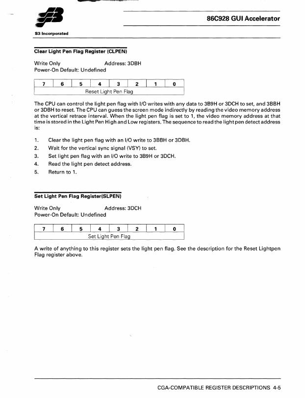
Clear Light Pen Flag Register (CLPEN)
Write Only Address: 3DBH Power-On Default: Undefined
7 6 5 4 3 2
Reset Light Pen Flag
86C928 GUI Accelerator
o
The CPU can control the light pen flag with I/O writes with any data to 3B9H or 3DCH to set, and 3BBH or 3DBH to reset. The CPU can guess the screen mode indirectly by reading the video memory address at the vertical retrace interval. When the light pen flag is set to 1, the video memory address at that time is stored in the Light Pen High and Low registers. The sequence to read the light pen detect address is:
1. Clear the light pen flag with an I/O write to 3BBH or 3DBH.
2. Wait for the vertical sync signal (VSY) to set.
3. Set light pen flag with an I/O write to 3B9H or 3DCH.
4. Read the light pen detect address.
5. Return to 1.
Set Light Pen Flag Register(SLPEN)
Write Only Address: 3DCH Power-On Default: Undefined
7 6 5 4 3 2 o Set Light Pen Flag
A write of anything to this register sets the light pen flag. See the description for the Reset Lightpen Flag register above.
CGA-COMPATIBLE REGISTER DESCRIPTIONS 4-5

.... r S3 Incorporated
86C928 GUI Accelerator
.'. 86C928 GUI Accelerator
S3 Incorporated
Section 5: MDA- and HGC-Compatible Register Descriptions
In the following register descriptions, "U" stands for undefined or unused and "R" stands for reserved (write = 0, read = U). See Appendix A for a table listing each register in this section and its page number.
Light Pen High Register (LPENH)
Read Only Address: 3B5H, Index 10H Power-On Default: Undefined
Refer to the description in Section 4.
Light Pen Low Register (LPENL)
Read Only Address: 3B5H, Index 11 H Power-On Default: Undefined
Refer to the description in Section 4.
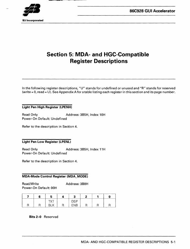
MDA-Mode Control Register (MDA_MODE)
ReadIWrite Address: 3B8H Power-On Default: OOH
I : I : i ~~ I : I ~;~ I : I R I : I
Bits 2-0 Reserved
MDA- AND HGC-COMPATIBLE REGISTER DESCRIPTIONS 5-1
53 Incorporated
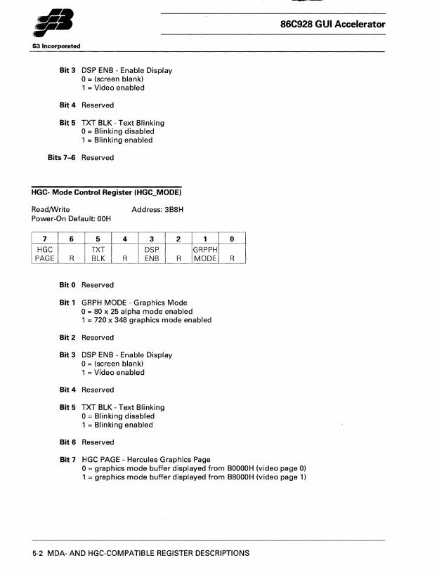
Bit 3 DSP ENB - Enable Display 0= (screen blank) 1 = Video enabled
Bit 4 Reserved
Bit 5 TXT BLK - Text Blinking 0= Blinking disabled 1 = Blinking enabled
Bits 7-6 Reserved
HGC- Mode Control Register (HGC_MODE)
Read/Write Address: 3B8H Power-On Default: OOH
7 6 5 4 3 2
HGC TXT DSP PAGE R BLK R ENB R
Bit 0 Reserved
Bit 1 GRPH MODE - Graphics Mode 0= 80 x 25 alpha mode enabled
1
GRPPH MODE
1 = 720 x 348 graphics mode enabled
Bit 2 Reserved
Bit 3 DSP ENB - Enable Display o = (screen blank) 1 = Video enabled
Bit 4 Reserved
Bit 5 TXT BLK - Text Blinking 0= Blinking disabled 1 = Blinking enabled
Bit 6 Reserved
Bit 7 HGC PAGE - Hercules Graphics Page
86C928 GUI Accelerator
0
R
o = graphics mode buffer displayed from BOOOOH (video page 0) 1 = graphics mode buffer displayed from B8000H (video page 1)
5-2 MDA- AND HGC-COMPATIBLE REGISTER DESCRIPTIONS
••
53 Incorporated
Set Light Pen Flag Register (HGC_SLPEN)
Write Only Address: 3B9H Power-On Default: Undefined
Refer to the description in Section 4.
HGC Status Register (HGC_STS)
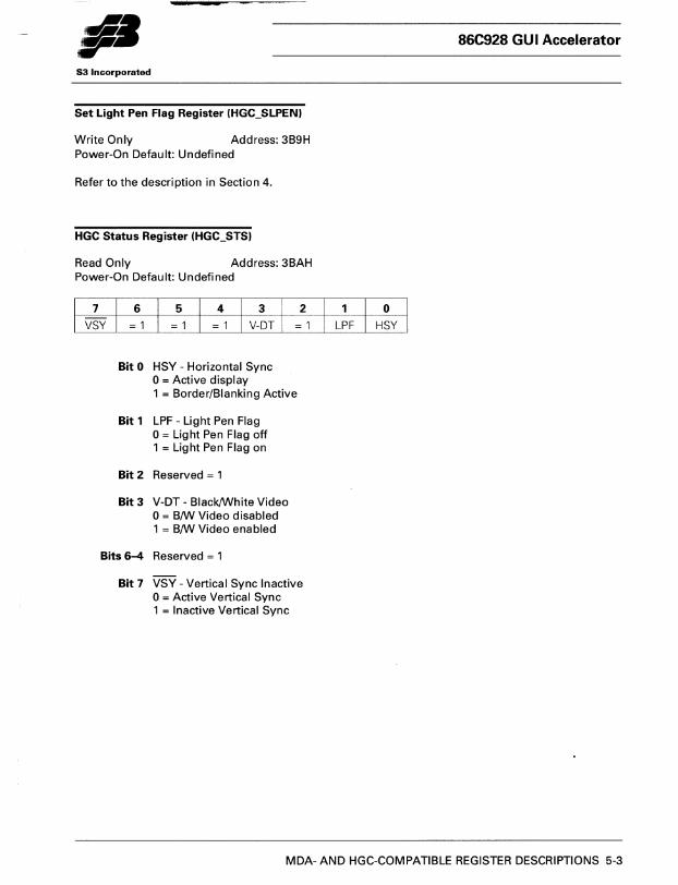
Read Only Address: 3BAH Power-On Default: Undefined
Bit 0 HSY - Horizontal Sync o = Active display 1 = Border/Blanking Active
Bit 1 LPF - Light Pen Flag 0= Light Pen Flag off 1 = Light Pen Flag on
Bit 2 Reserved = 1
Bit 3 V-DT - Black/White Video 0= BNI/ Video disabled 1 = BNI/ Video enabled
Bits 6-4 Reserved = 1
Bit 7 VSY - Vertical Sync Inactive 0= Active Vertical Sync 1 = Inactive Vertical Sync
86C928 GUI Accelerator
o LPF HSY
MDA- AND HGC-COMPATIBLE REGISTER DESCRIPTIONS 5-3
S3 Incorporated
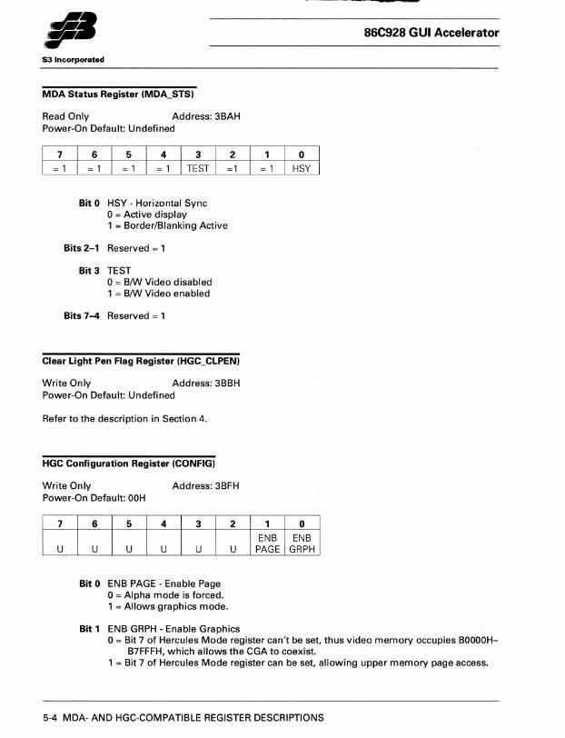
MDA Status Register (MDA_STS)
Read Only Address: 3BAH Power-On Default: Undefined
Bit 0 HSY - Horizontal Sync o = Active display 1 = Border/Blanking Active
Bits 2-1 Reserved = 1
Bit 3 TEST o = BNoI Video disabled 1 = BNoI Video enabled
Bits 7-4 Reserved = 1
Clear Light Pen Flag Register (HGC_CLPEN)
Write Only Address: 3BBH Power-On Default: Undefined
Refer to the description in Section 4.
HGC Configuration Register (CONFIG)
Write Only Address: 3BFH Power-On Default: OOH
7
U
6 5 4 3
U U U U
Bit 0 ENB PAGE - Enable Page 0= Alpha mode is forced. 1 = Allows graphics mode.
2
U
Bit 1 ENB GRPH - Enable Graphics
86C928 GUI Accelerator
o = 1 HSY
1 0
ENS ENS PAGE GRPH
0= Bit 7 of Hercules Mode register can't be set, thus video memory occupies BOOOOHB7FFFH, which allows the CGA to coexist.
1 = Bit 7 of Hercules Mode register can be set, allowing upper memory page access.
5-4 MDA- AND HGC-COMPATIBLE REGISTER DESCRIPTIONS
.. 86C928 GUI Accelerator
53 Incorporated
Section 6: VGA Standard Register Descriptions
In the following register descriptions, 'U' stands for undefined or unused and 'R' stands for reserved (write = 0, read = U). A question mark in an address stands for a hexadecimal value of either '8' or 'D'. If bit 0 of the Miscellaneous Output Register (3C2H, Write) is set to 1, the address is based at 3DxH for color emulation. If this bit is reset to 0, the address is based at 38xH for monochrome emulation.
See Appendix A for a table listing each register in this section and its page number.
6.1 GENERAL REGISTERS
This section describes general input status and output control registers.
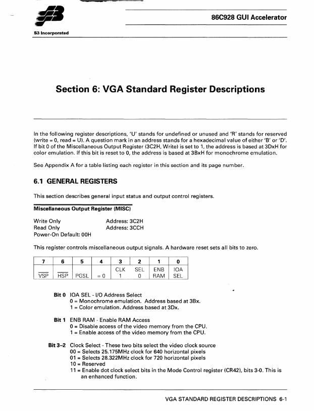
Miscellaneous Output Register (MiSe)
Write Only Read Only
Address: 3C2H Address: 3CCH
Power-On Default: OOH
This register controls miscellaneous output signals. A hardware reset sets all bits to zero.
7 6 5 4 3 I 2 1 0
elK SEl ENB lOA -- --VSP HSP PGSl =0 1 0 RAM SEl
Bit 0 lOA SEl - I/O Address Select 0= Monochrome emulation. Address based at 38x. 1 = Color emulation. Address based at 3Dx.
Bit 1 EN8 RAM - Enable RAM Access 0= Disable access of the video memory from the CPU. 1 = Enable access of the video memory from the CPU.
Bit 3-2 Clock Select - These two bits select the video clock source 00 = Selects 25.175MHz clock for 640 horizontal pixels 01 = Selects 28.322MHz clock for 720 horizontal pixels 10 = Reserved 11 = Enable dot clock select bits in the Mode Control register (CR42), bits 3-0. This is
an enhanced function.
VGA STANDARD REGISTER DESCRIPTIONS 6-1
• .lta ,. S3 Incorporated
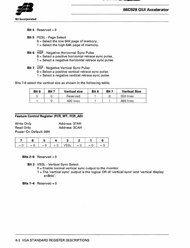
Bit 4 Reserved = 0
Bit 5 PGSL - Page Select 0= Select the low 64K page of memory. 1 = Select the high 64K page of memory.
Bit 6 HSP - Negative Horizontal Sync Pulse 0= Select a positive horizontal retrace sync pulse. 1 = Select a negative horizontal retrace sync pulse.
Bit 7 VSP - Negative Vertical Sync Pulse 0= Select a positive vertical retrace sync pulse. 1 = Select a negative vertical retrace sync pulse.
Bits 7-6 select the vertical size as shown in the following table;
Bit 6 Bit 7 Vertical size
0 0 Reserved
1 0 400 lines
Feature Control Register (FCR_WT, FCR_AD)
Write Only Read Only Power-On Default: OOH
Bits 2-0 Reserved = 0
Address: 3?AH Address: 3CAH
Bit 3 VSSL - Vertical Sync Select
Bit 6 Bit7
1 0
1 1
o =0 =0
0= Enable normal vertical sync output to the monitor
-86C928 GUI Accelerator
Vertical Size
350 lines
480 lines
1 = The 'vertical sync' output is the logical OR of 'vertical sync' and 'vertical display enllble'.
Bits 7-4 Reserved = 0
6-2 VGA STANDARD REGISTER DESCRIPTIONS
S3 Incorporated
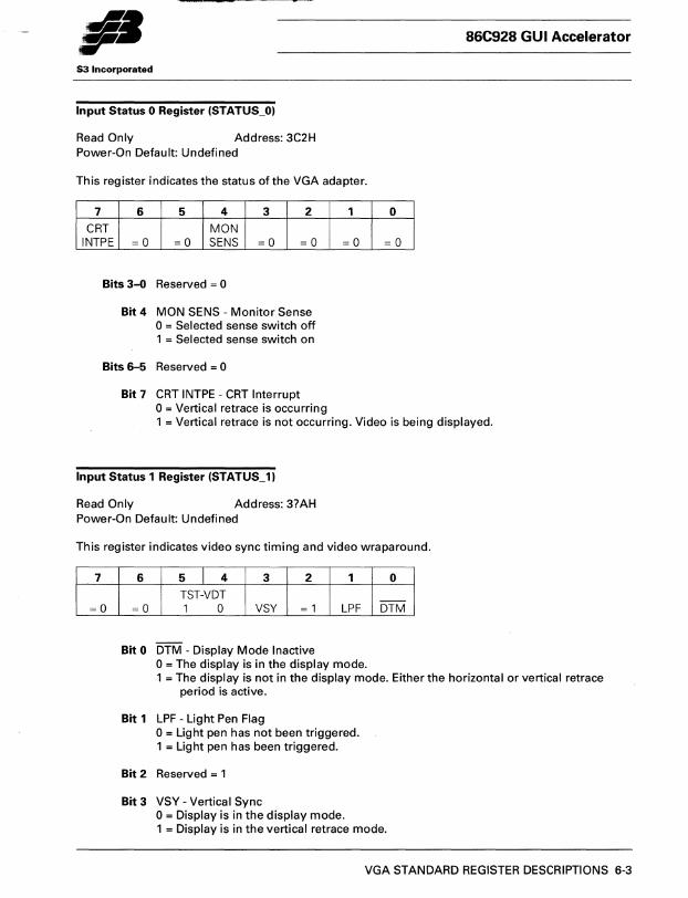
Input Status 0 Register (STATUS_O)
Read Only Address: 3C2H Power-On Default: Undefined
This register indicates the status of the VGA adapter.
7 6 5 4 3 2 CRT MON
INTPE =0 =0 SENS =0 =0
Bits 3-0 Reserved = 0
Bit 4 MON SENS - Monitor Sense o = Selected sense switch off 1 = Selected sense switch on
Bits 6-5 Reserved = 0
Bit 7 CRT INTPE - CRT Interrupt 0= Vertical retrace is occurring
1
=0
86C928 GUI Accelerator
0
=0
1 = Vertical retrace is not occurring. Video is being displayed.
Input Status 1 Register (STATUS_1)
Read Only Address: 3?AH Power-On Default: Undefined
This register indicates video sync timing and video wraparound.
7
=0
6 5 I 4 3 2 1 ° TST-VDT --=0 1 0 VSY = 1 LPF DTM
Bit 0 DTM - Display Mode Inactive o = The display is in the display mode. 1 = The display is not in the display mode. Either the horizontal or vertical retrace
period is active.
Bit 1 LPF - Light Pen Flag 0= Light pen has not been triggered. 1 = Light pen has been triggered.
Bit 2 Reserved = 1
Bit 3 VSY - Vertical Sync o = Display is in the display mode. 1 = Display is in the vertical retrace mode.
VGA STANDARD REGISTER DESCRIPTIONS 6-3
•• r 86C928 GUI Accelerator
S3 Incorporated
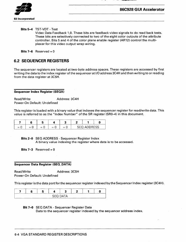
Bits 5-4 TST-VDT - Test Video Data Feedback 1,0. These bits are feedback video signals to do read back tests. These bits are selectively connected to two of the eight color outputs ofthe attribute controller. Bits 5 and 4 of the color plane enable register (AR12) control the multiplexer for this video output wrap wiring.
Bits 7-6 Reserved = ° 6.2 SEQUENCER REGISTERS
The sequencer registers are located at two-byte address spaces. These registers are accessed by first writing the data to the index register ofthe sequencer at I/O address 3C4H and then writing to or reading from the data register at 3C5H.
Sequencer Index Register (SEOX)
ReadIWrite Address: 3C4H Power-On Default: Undefined
This register is loaded with a binary value that indexes the sequencer register for read/write data. This value is referred to as the "Index Number" ofthe SR register (SRO-4) in this document.
210
SEQ ADDRESS
Bits 2-0 SEQ ADDRESS - Sequencer Register Index A binary value indexing the register where data is to be accessed.
Bits 7-3 Reserved = °
Sequencer Data Register (SEQ_DATA)
ReadIWrite Address: 3C5H Power-On Default: Undefined
This register isthe data portforthe sequencer register indexed by the Sequencer Index register (3C4H).
7 6 5 4 3 2 o SEQ DATA
Bit 7-0 SEQ DATA - Sequencer Register Data Data to the sequencer register indexed by the sequencer address index.
6-4 VGA STANDARD REGISTER DESCRIPTIONS
53 Incorporated
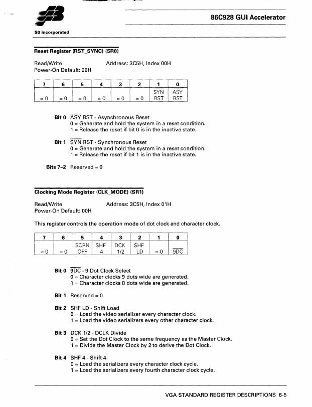
Reset Register (RST_SYNC) (SRO)
ReadIWrite Address: 3C5H, Index OOH Power-On Default: OOH
Bit 0 ASY RST - Asynchronous Reset 0= Generate and hold the system in a reset condition. 1 = Release the reset if bit 0 is in the inactive state.
Bit 1 SYN RST - Synchronous Reset 0= Generate and hold the system in a reset condition. 1 = Release the reset if bit 1 is in the inactive state.
Bits 7-2 Reserved = 0
Clocking Mode Register (ClK_MODE) (SR1)
ReadIWrite Address: 3C5H, Index 01 H Power-On Default: OOH
86C928 GUI Accelerator
This register controls the operation mode of dot clock and character clock.
7
=0
6 5 4 3 2 1 0
SCRN SHF DCK SHF --=0 OFF 4 1/2 LD =0 9DC
Bit 0 9DC - 9 Dot Clock Select 0= Character clocks 9 dots wide are generated. 1 = Character clocks 8 dots wide are generated.
Bit 1 Reserved = 0
Bit 2 SHF LD - Shift Load 0= Load the video serializer every character clock. 1 = Load the video serializers every other character clock.
Bit 3 DCK 1/2 - DCLK Divide 0= Set the Dot Clock to the same frequency as the Master Clock. 1 = Divide the Master Clock by 2 to derive the Dot Clock.
Bit 4 SHF 4 - Shift 4 0= Load the serializers every character clock cycle. 1 = Load the serializers every fourth character clock cycle.
VGA STANDARD REGISTER DESCRIPTIONS 6-5
S3 Incorporated
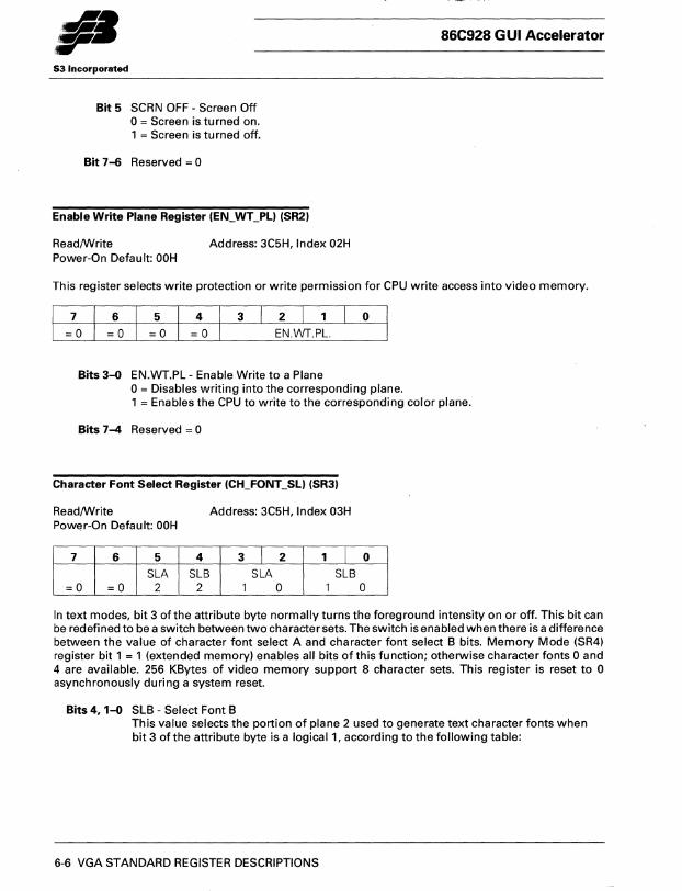
Bit 5 SCRN OFF - Screen Off 0= Screen is turned on. 1 = Screen is turned off.
Bit 7-6 Reserved = 0
Enable Write Plane Register (EN_WT_PLI (SR2)
Read/Write Address: 3C5H, Index 02H Power-On Default: OOH
-86C928 GUI Accelerator
This register selects write protection or write permission for CPU write access into video memory.
3 2 1 o EN.wT.PL.
Bits 3-0 EN.WT.PL - Enable Write to a Plane 0= Disables writing into the corresponding plane. 1 = Enables the CPU to write to the corresponding color plane.
Bits 7-4 Reserved = 0
Character Font Select Register (CH_FONT _SL) (SR3)
Read/Write Address: 3C5H, Index 03H Power-On Default: OOH
7 6 5 4 3 I 2 1 I 0
SLA SLB SLA SLB =0 =0 2 2 1 0 1 0
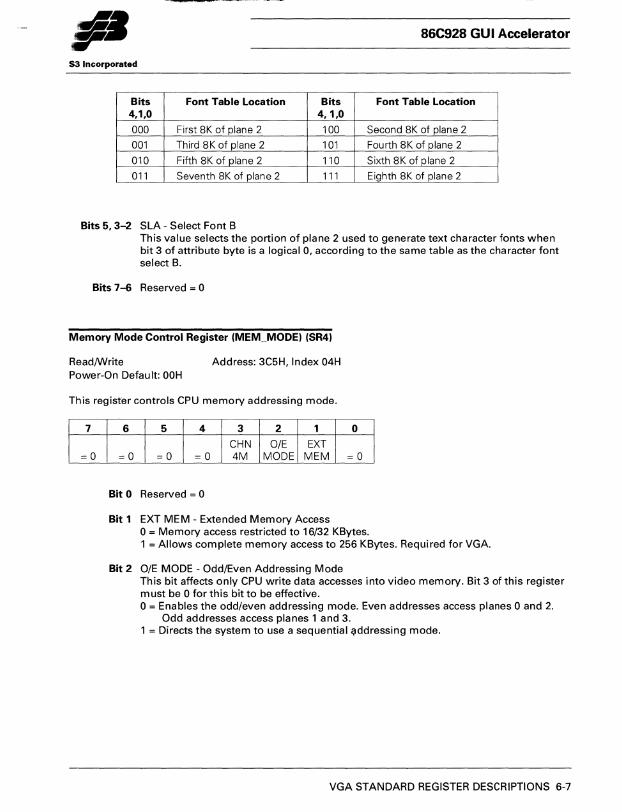
In text modes, bit 3 of the attribute byte normally turns the foreground intensity on or off. This bit can be redefined to be a switch between two character sets. The switch is enabled when there is a difference between the value of character font select A and character font select B bits. Memory Mode (SR4) register bit 1 = 1 (extended memory) enables all bits of this function; otherwise character fonts 0 and 4 are available. 256 KBytes of video memory support 8 character sets. This register is reset to 0 asynchronously during a system reset.
Bits 4, 1-0 SLB - Select Font B This value selects the portion of plane 2 used to generate text character fonts when bit 3 of the attribute byte is a logical 1, according to the following table:
6-6 VGA STANDARD REGISTER DESCRIPTIONS
86C928 GUI Accelerator
53 Incorporated
Bits Font Table Location Bits Font Table Location 4,1,0 4,1,0
000 First 8K of plane 2 100 Second 8K of plane 2
001 Third 8K of plane 2 101 Fourth 8K of plane 2
010 Fifth 8K of plane 2 110 Sixth 8K of plane 2
011 Seventh 8K of plane 2 111 Eighth 8K of plane 2
Bits 5, 3-2 SLA - Select Font B This value selects the portion of plane 2 used to generate text character fonts when bit 3 of attribute byte is a logical 0, according to the same table as the character font select B.
Bits 7-6 Reserved = 0
Memory Mode Control Register (MEM_MODE) (SR4)
ReadIWrite Address: 3C5H, Index 04H Power-On Default: OOH
This register controls CPU memory addressing mode.
7
=0
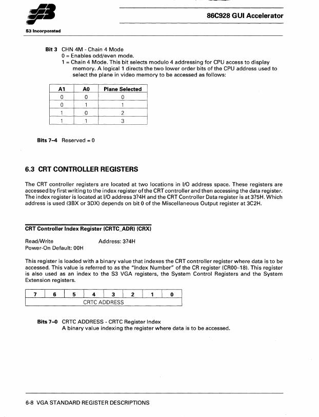
6 5 4 3 2 1 ° CHN OlE EXT =0 =0 =0 4M MODE MEM =0
Bit ° Reserved = 0
Bit 1 EXT MEM - Extended Memory Access o = Memory access restricted to 16/32 KBytes. 1 = Allows complete memory access to 256 KBytes. Required for VGA.
Bit 2 OlE MODE - Odd/Even Addressing Mode This bit affects only CPU write data accesses into video memory. Bit 3 of this register must be 0 for this bit to be effective. 0= Enables the odd/even addressing mode. Even addresses access planes 0 and 2.
Odd addresses access planes 1 and 3. 1 = Directs the system to use a sequential qddressing mode.
VGA STANDARD REGISTER DESCRIPTIONS 6-7
86C928 GUI Accelerator
53 Incorporated
Bit 3 CHN 4M - Chain 4 Mode o = Enables odd/even mode. 1 = Chain 4 Mode. This bit selects modulo 4 addressing for CPU access to display
memory. A logical 1 directs the two lower order bits of the CPU address used to select the plane in video memory to be accessed as follows:
A1 AO Plane Selected
0 0 0
0 1 1
1 0 2
1 1 3
Bits 7-4 Reserved = 0
6.3 CRT CONTROLLER REGISTERS
The CRT controller registers are located at two locations in I/O address space. These registers are accessed by first writing to the index register ofthe CRT controller and then accessing the data register. The index register is located at I/O address 3?4H and the CRT Controller Data register is at 3?5H. Which address is used (3BX or 3DX) depends on bit 0 of the Miscellaneous Output register at 3C2H.
CRT Controller Index Register (CRTC_ADR) (CRX)
Read/Write Address: 3?4H Power-On Default: OOH
This register is loaded with a binary value that indexes the CRT controller register where data is to be accessed. This value is referred to as the "Index Number" of the CR register (CROO-18). This register is also used as an index to the S3 VGA registers, the System Control Registers and the System Extension registers.
7 6 5 432 o CRTC ADDRESS
Bits 7--0 CRTC ADDRESS - CRTC Register Index A binary value indexing the register where data is to be accessed.
6-8 VGA STANDARD REGISTER DESCRIPTIONS
86C928 GUI Accelerator
53 Incorporated
CRT Controller Data Register (CRTC_DATA) (CRT)
ReadIWrite Address: 3?5H Power-On Default: Undefined
This register is the data port for the CRT controller register indexed by the CRT Controller Address register.
7 6 5 4 3 2 1 o CRTC DATA
Bits 7-0 CRTC DATA - CRTC Register Data Data to the CRT controller register indexed by the CRT controller address index.
Horizontal Total Register (H_TOTAL) (CRO)
ReadIWrite Address: 3?5H, Index OOH Power-On Default: Undefined
This register defines the number of characters in the horizontal scan interval including retrace time.
7 6 5 4 3 2 o HORIZONTAL TOTAL
Bits 7-0 HORIZONTAL TOTAL. The total number characters - 5. The value controls the period of the horizontal retrace output signal. An internal horizontal character clock inputs to the CRT Controller, and all horizontal and vertical timings are based upon this register. Comparators are used to compare register values with horizontal character values to provide horizontal timings.
Horizontal Display End Register (H_D_END) (CR1)
ReadIWrite Address: 3?5H, Index 01 H Power-On Default: Undefined
This register defines the number of characters to be displayed per horizontal line.
7 6 5 4 3 2 o HORIZONTAL DISPLAY END
Bits 7-0 HORIZONTAL DISPLAY END A value one less than the total number of displayed characters.
VGA STANDARD REGISTER DESCRIPTIONS 6-9
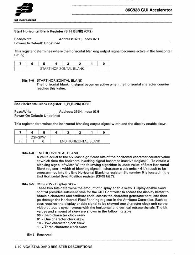
•• r 86C928 GUI Accelerator
S3 Incorporated
Start Horizontal Blank Register (S_H_BLNK) (CR2)
ReadIWrite Address: 3?5H, Index 02H Power-On Default: Undefined
This register determines where the horizontal blanking output signal becomes active in the horizontal timing.
7 6 5 4 3 2 o START HORIZONTAL BLANK
Bits 7-0 START HORIZONTAL BLANK The horizontal blanking signal becomes active when the horizontal character counter reaches this value.
End Horizontal Blank Register (E_H_BLNK) (CR3)
ReadIWrite Address: 3?5H, Index 03H Power-On Default: Undefined
This register determines the horizontal blanking output signal width and the display enable skew.
7
R
6 I 5 4 I 3 I 2 I 1 I 0 DSP-SKW 1 0 END HORIZONTAL BLANK
Bits 4-0 END HORIZONTAL BLANK A value equal to the six least-significant bits of the horizontal character counter value at which time the horizontal blanking signal becomes inactive (logical 0). To obtain a blanking signal of width W, the following algorithm is used: value of Start Horizontal Blank register + width of blanking signal in character clock units = 6-bit result to be programmed into the End Horizontal Blanking register. Bit number 5 is located in the End Horizontal Sync Position register (CR05 bit 7).
Bits 6-5 DSP-SKW - Display Skew These two bits determine the amount of display enable skew. Display enable skew control provides sufficient time for the CRT Controller to access the display buffer to obtain a character and attribute code, access the character generator font, and then go through the Horizontal Pixel Panning register in the Attribute Controller. Each access requires the display enable signal to be skewed one character clock unit so the video output is synchronous with the horizontal and vertical retrace signals. The bit values and amount of skew are shown in the following table: 00 = Zero character clock skew 01 = One character clock skew 10 = Two character clock skew 11 = Three character clock skew
Bit 7 Reserved
6-10 VGA STANDARD REGISTER DESCRIPTIONS
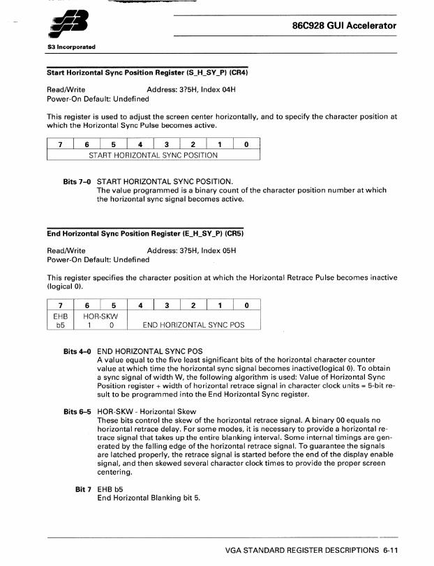
•• r 86C928 GUI Accelerator
S3 Incorporated
Start Horizontal Sync Position Register (S_H_SY _PI (CR41
ReadIWrite Address: 3?5H, Index 04H Power-On Default: Undefined
This register is used to adjust the screen center horizontally, and to specify the character position at which the Horizontal Sync Pulse becomes active.
Bits 7-0 START HORIZONTAL SYNC POSITION. The value programmed is a binary count of the character position number at which the horizontal sync signal becomes active.
End Horizontal Sync Position Register (E_H_SY _PI (CR51
ReadIWrite Address: 3?5H, Index 05H Power-On Default: Undefined
This register specifies the character position at which the Horizontal Retrace Pulse becomes inactive (logical 0).
7 6 I 5 4 I 3 I 2 I 1 I 0
EHB HOR-SKW b5 1 0 END HORIZONTAL SYNC POS
Bits 4-0 END HORIZONTAL SYNC POS A value equal to the five least significant bits of the horizontal character counter value at which time the horizontal sync signal becomes inactive(logical 0). To obtain a sync signal of width W, the following algorithm is used: Value of Horizontal Sync Position register + width of horizontal retrace signal in character clock units = 5-bit result to be programmed into the End Horizontal Sync register.
Bits 6--5 HOR-SKW - Horizontal Skew These bits control the skew of the horizontal retrace signal. A binary 00 equals no horizontal retrace delay. For some modes, it is necessary to provide a horizontal retrace signal that takes up the entire blanking interval. Some internal timings are generated by the falling edge of the horizontal retrace signal. To guarantee the signals are latched properly, the retrace signal is started before the end of the display enable signal, and then skewed several character clock times to provide the proper screen centering.
Bit7 EHB b5 End Horizontal Blanking bit 5.
VGA STANDARD REGISTER DESCRIPTIONS 6-11
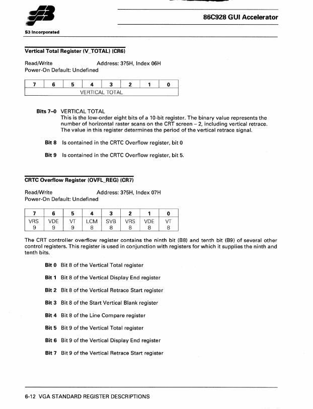
86C928 GUI Accelerator
S3 Incorporated
Vertical Total Register (V_TOTAL) (CR6)
ReadIWrite Address: 3?5H, Index 06H Power-On Default: Undefined
7 6 5 4 3 2 o VERTICAL TOTAL
Bits 7-0 VERTICAL TOTAL This is the low-order eight bits of a 10-bit register. The binary value represents the number of horizontal raster scans on the CRT screen - 2, including vertical retrace. The value in this register determines the period of the vertical retrace signal.
Bit 8 Is contained in the CRTC Overflow register, bit 0
Bit 9 Is contained in the CRTC Overflow register, bit 5.
CRTC Overflow Register (OVFL_REG) (CR7)
ReadIWrite Address: 3?5H, Index 07H Power-On Default: Undefined
7 6 5 4 3 2 1 0 VRS VDE VT LCM SVB VRS VDE VT
9 9 9 8 8 8 8 8
The CRT controller overflow register contains the ninth bit (B8) and tenth bit (B9) of several other control registers. This register is used in conjunction with registers for which it supplies the ninth and tenth bits.
Bit 0 Bit 8 of the Vertical Total register
Bit 1 Bit 8 of the Vertical Display End register
Bit 2 Bit 8 of the Vertical Retrace Start register
Bit 3 Bit 8 ofthe Start Vertical Blank register
Bit 4 Bit 8 of the Line Compare register
Bit 5 Bit 9 of the Vertical Total register
Bit 6 Bit 9 of the Vertical Display End register
Bit 7 Bit 9 of the Vertical Retrace Start register
6-12 VGA STANDARD REGISTER DESCRIPTIONS
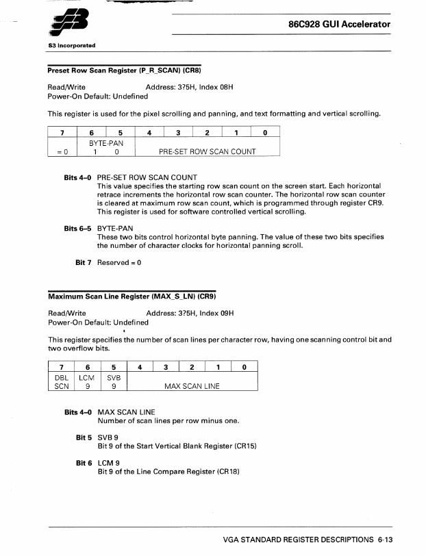
86C928 GUI Accelerator
53 Incorporated
Preset Row Scan Register (P _R_SCAN) (CR8)
Read/Write Address: 3?5H, Index 08H Power-On Default: Undefined
This register is used for the pixel scrolling and panning, and text formatting and vertical scrolling.
7 6 I 5 4 I 3 I 2 I 1 I 0
BYTE-PAN =0 1 0 PRE-SET ROW SCAN COUNT
Bits 4-0 PRE-SET ROW SCAN COUNT This value specifies the starting row scan count on the screen start. Each horizontal retrace increments the horizontal row scan counter. The horizontal row scan counter is cleared at maximum row scan count, which is programmed through register CR9. This register is used for software controlled vertical scrolling.
Bits 6-5 BYTE-PAN These two bits control horizontal byte panning. The value ofthese two bits specifies the number of character clocks for horizontal panning scroll.
Bit 7 Reserved = 0
Maximum Scan Line Register (MA)CS_LN) (CR9)
Read/Write Address: 3?5H, Index 09H Power-On Default: Undefined
This register specifies the number of scan lines per character row, having one scanning control bit and two overflow bits.
7 6 5 4 I 3 I 2 I 1 I 0
DBL LCM SVB SCN 9 9 MAX SCAN LINE
Bits 4-0 MAX SCAN LINE Number of scan lines per row minus one.
Bit 5 SVB 9 Bit 9 of the Start Vertical Blank Register (CR15)
Bit 6 LCM 9 Bit 9 of the Line Compare Register (CR 18)
VGA STANDARD REGISTER DESCRIPTIONS 6-13
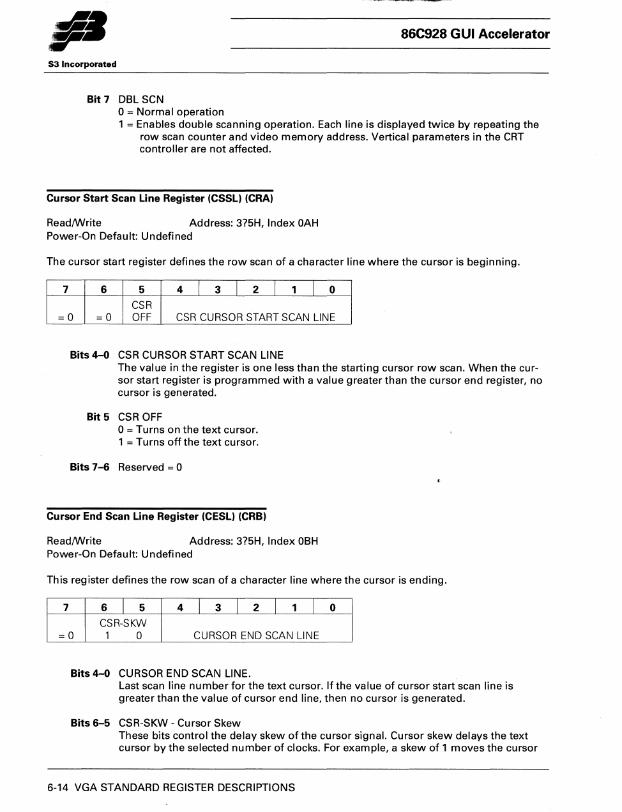
AI
86C928 GUI Accelerator
S3 Incorporated
Bit 7 DBL SCN 0= Normal operation 1 = Enables double scanning operation. Each line is displayed twice by repeating the
row scan counter and video memory address. Vertical parameters in the CRT controller are not affected.
Cursor Start Scan Line Register (CSSL) (CRA)
Read/Write Address: 3?5H, Index OAH Power-On Default: Undefined
The cursor start register defines the row scan of a character line where the cursor is beginning.
7 6 5 4 I 3 I 2 I 1 I 0 CSR
=0 =0 OFF CSR CURSOR START SCAN LINE
Bits 4-0 CSR CURSOR START SCAN LINE The value in the register is one less than the starting cursor row scan. When the cursor start register is programmed with a value greater than the cursor end register, no cursor is generated.
Bit 5 CSR OFF 0= Turns on the text cursor. 1 = Turns off the text cursor.
Bits 7-6 Reserved = 0
Cursor End Scan Line Register (CESL) (CRB)
Read/Write Address: 3?5H, Index OBH Power-On Default: Undefined
This register defines the row scan of a character line where the cursor is ending.
7 6 I 5 4 I 3 I 2 I 1 I 0
CSR-SKW =0 1 0 CURSOR END SCAN LINE
Bits 4-0 CURSOR END SCAN LINE. Last scan line number for the text cursor. If the value of cursor start scan line is greater than the value of cursor end line, then no cursor is generated.
Bits 6-5 CSR-SKW - Cursor Skew These bits control the delay skew ofthe cursor signal. Cursor skew delays the text cursor by the selected number of clocks. For example, a skew of 1 moves the cursor
6-14 VGA STANDARD REGISTER DESCRIPTIONS
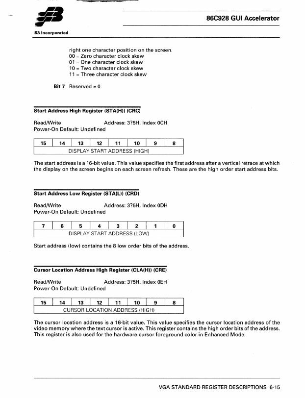
fl· 53 Incorporated
-
right one character position on the screen. 00 = Zero character clock skew 01 = One character clock skew 10 = Two character clock skew 11 = Three character clock skew
Bit 7 Reserved = 0
Start Address High Register (STA(H)) (CRC)
ReadlWrite Address: 3?5H, Index OCH Power-On Default: Undefined
86C928 GUI Accelerator
The start address is a 16-bit value. This value specifies the first address after a vertical retrace at which the display on the screen begins on each screen refresh. These are the high order start address bits.
Start Address Low Register (STA(L)) (CRD)
ReadlWrite Address: 3?5H, Index ODH Power-On Default: Undefined
7 6 5 4 3 2 o DISPLAY START ADDRESS (LOW)
Start address (low) contains the 8 low order bits of the address.
Cursor Location Address High Register (CLA(H)) (CRE)
ReadlWrite Address: 3?5H, Index OEH Power-On Default: Undefined
The cursor location address is a 16-bit value. This value specifies the cursor location address ofthe video memory where the text cursor is active. This register contains the high order bits of the address. This register is also used for the hardware cursor foreground color in Enhanced Mode.
VGA STANDARD REGISTER DESCRIPTIONS 6-15
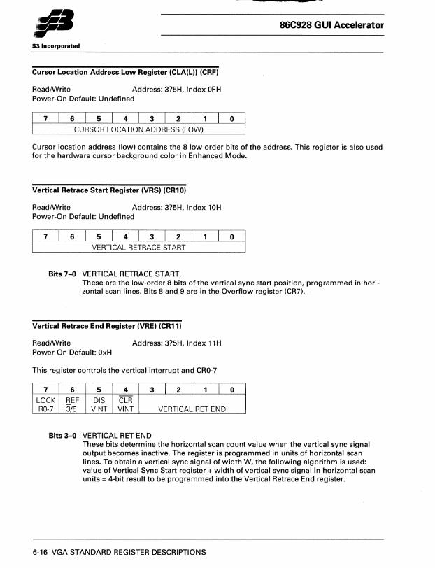
86C928 GUI Accelerator
S3 Incorporated
Cursor Location Address Low Register (CLA(LII (CRF)
Read/Write Address: 3?5H, Index OFH Power-On Default: Undefined
Cursor location address (low) contains the 8 low order bits of the address. This register is also used for the hardware cursor background color in Enhanced Mode.
Vertical Retrace Start Register (VRS) (CR10)
Read/Write Address: 3?5H, Index 10H Power-On Default: Undefined
7 6 o VERTICAL RETRACE START
Bits 7-0 VERTICAL RETRACE START. These are the low-order 8 bits of the vertical sync start position, programmed in horizontal scan lines. Bits 8 and 9 are in the Overflow register (CR7).
Vertical Retrace End Register (VRE) (CR11)
Read/Write Address: 3?5H, Index 11 H Power-On Default: OxH
This register controls the vertical interrupt and CRO-7
7 6 5 4 3 I 2 I 1 I 0 LOCK REF DIS CLR RO-7 3/5 VINT VINT VERTICAL RET END
Bits 3-0 VERTICAL RET END These bits determine the horizontal scan count value when the vertical sync signal output becomes inactive. The register is programmed in units of horizontal scan lines. To obtain a vertical sync signal of width W, the following algorithm is used: value of Vertical Sync Start register + width of vertical sync signal in horizontal scan units = 4-bit result to be programmed into the Vertical Retrace End register.
6-16 VGA STANDARD REGISTER DESCRIPTIONS
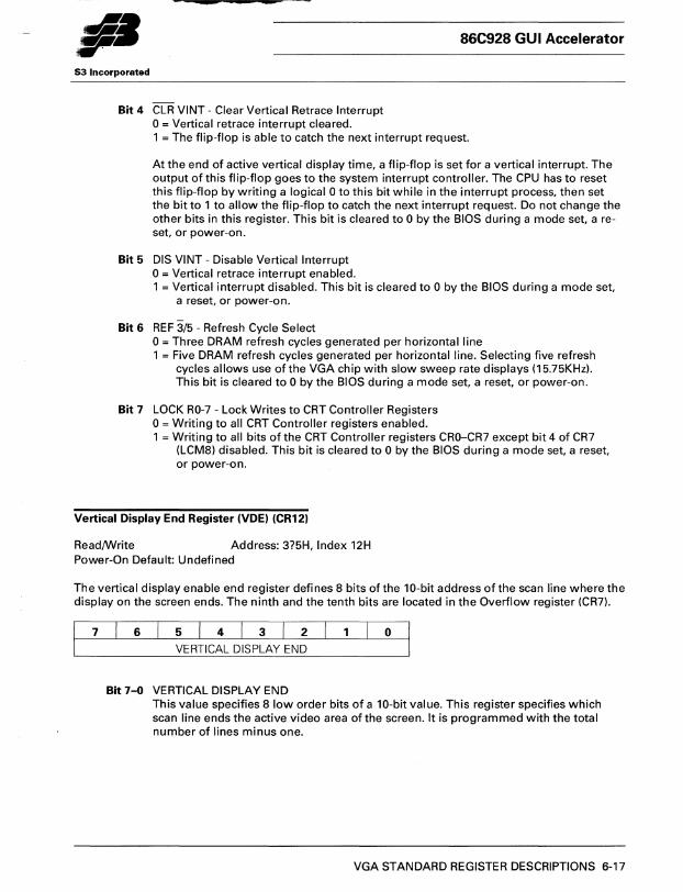
86C928 GUI Accelerator
S3 Incorporated
Bit 4 CLR VINT - Clear Vertical Retrace Interrupt 0= Vertical retrace interrupt cleared. 1 = The flip-flop is able to catch the next interrupt req uest.
At the end of active vertical display time, a flip-flop is set for a vertical interrupt. The output of this flip-flop goes to the system interrupt controller. The CPU has to reset this flip-flop by writing a logical 0 to this bit while in the interrupt process, then set the bit to 1 to allow the flip-flop to catch the next interrupt request. Do not change the other bits in this register. This bit is cleared to 0 by the BIOS during a mode set, a reset, or power-on.
Bit 5 DIS VINT - Disable Vertical Interrupt 0= Vertical retrace interrupt enabled. 1 = Vertical interrupt disabled. This bit is cleared to 0 by the BIOS during a mode set,
a reset, or power-on.
Bit 6 REF 3/5 - Refresh Cycle Select 0= Three DRAM refresh cycles generated per horizontal line 1 = Five DRAM refresh cycles generated per horizontal line. Selecting five refresh
cycles allows use ofthe VGA chip with slow sweep rate displays (15.75KHz). This bit is cleared to 0 by the BIOS during a mode set, a reset, or power-on.
Bit 7 LOCK RO-7 - Lock Writes to CRT Controller Registers o = Writing to all CRT Controller registers enabled. 1 = Writing to all bits of the CRT Controller registers CRO-CR7 except bit 4 of CR7
(LCM8) disabled. This bit is cleared to 0 by the BIOS during a mode set, a reset, or power-on.
Vertical Display End Register (VDE) (CR12)
ReadIWrite Address: 3?5H, Index 12H Power-On Default: Undefined
The vertical display enable end register defines 8 bits of the 10-bit address of the scan line where the display on the screen ends. The ninth and the tenth bits are located in the Overflow register (CR7).
7 6 543 2 o VERTICAL DISPLAY END
Bit 7-0 VERTICAL DISPLAY END This value specifies 8 low order bits of a 10-bit value. This register specifies which scan line ends the active video area of the screen. It is programmed with the total number of lines minus one.
VGA STANDARD REGISTER DESCRIPTIONS 6-17
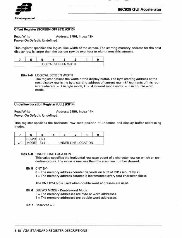
-86C928 GUI Accelerator
S3 Incorporated
Offset Register (SCREEN-OFFSET) (CR13)
Read/Write Address: 3?5H, Index 13H Power-On Default: Undefined
This register specifies the logical line width of the screen. The starting memory address for the next display row is larger than the current row by two, four or eight times this amount.
7 6 5 432 o LOGICAL SCREEN WIDTH
Bits 7-0 LOGICAL SCREEN WIDTH The register defines the width ofthe display buffer. The byte starting address ofthe next display row is the byte starting address of current row + k* (contents of this register) where k = 2 in byte mode, k = 4 in word mode and k = 8 in double word mode.
Underline Location Register (ULl) (CR14)
Read/Write Address: 3?5H, Index 14H Power-On Default: Undefined
This register specifies the horizontal row scan position of underline and display buffer addressing modes.
7 6 5 4 I 3 I 2 I 1 I 0 DBWD CNT
=0 MODE BY4 UNDER LINE LOCATION
Bits 4-0 UNDER LINE LOCATION This value specifies the horizontal row scan count of a character rowan which an underline occurs. The value is one less than the scan line number desired.
Bit 5 CNT BY4 0= The memory address counter depends on bit 3 of CR17 (count by 2). 1 = The memory address counter is incremented every four character clocks.
The CNT BY4 bit is used when double word addresses are used.
Bit 6 DBLWD MODE - Doubleword Mode 0= The memory addresses are byte or word addresses. 1 = The memory addresses are double word addresses.
Bit 7 Reserved = 0
6-18 VGA STANDARD REGISTER DESCRIPTIONS
-86C928 GUI Accelerator
53 Incorporated
Start Vertical Blank Register (SVBI (CR151
Read/Write Address: 3?5H, Index 15H Power-On Default: Undefined
7 6 5 4 3 2 o START VERTICAL BLANK
Bits 7-0 START VERTICAL BLANK. These are low 8 bits of a 10-bit register.
Bit 8 Is in the Overflow register (CR7).
Bit 9 Is in the Maximum Scan Line register (CR9). The value of these 10 bits is one less than the horizontal scan line count at which the vertical blanking signal becomes active.
End Vertical Blank Register (EVBI (CR161
Read/Write Address: 3?5H, Index 16H Power-On Default: Undefined
7 6 543 2 o END VERTICAL BLANK
Bits 7-0 END VERTICAL BLANK This register specifies the horizontal scan count value when the vertical blank signal output becomes inactive. The register is programmed in units of horizontal scan lines.
To obtain a width of vertical blank signal W, the following algorithm is used: (Value of Start Vertical Blank register minus 1 I + width of vertical blank signal in horizontal scan units = 8-bit result to be programmed into the End Vertical Blank register.
VGA STANDARD REGISTER DESCRIPTIONS 6-19
.... --86C928 GUI Accelerator
53 Incorporated
CRTC Mode Control Register (CRT_MOl (CR171
ReadIWrite Address: 3?5H, Index 17H Power-On Default: OOH
This register is a multifunction control register, with each bit defining a different specification.
7
-RST
6 5 4 3 2 1 0 BYTE ADW CNT VT 4BK 2BK
MODE 16K =0 BY2 X2 HGC CGA
Bit 0 2BK CGA - Bank 2 Mode for CGA Emulation 0= Row scan counter bit 0 is substituted for memory address bit 13 during active
display time. 1 = Memory address bit 13 appears on the memory address output bit 13 signal of
the CRT controller.
This bit allows memory mapping compatibility with the IBM CGA graphics mode.
Bit 1 4BK HGC - Bank 4 Mode for HGA Emulation 0= Row scan counter bit 1 is substituted for memory address bit 14 during active
display time. 1 = Memory address bit 14 appears on the memory address output bit 14 signal of
the CRT controller.
The combination of this bit and bit 0 of this register allows compatibility with Hercules HGC graphics memory mapping.
Bit 2 VT X2 - Vertical Total Double Mode 0= Horizontal retrace clock selected. 1 = Horizontal retrace clock divided by two selected.
This bit selects horizontal retrace clock or horizontal retrace clock divided by two as the clock that controls the vertical timing counter. If the vertical retrace counter is clocked with the horizontal retrace clock divided by 2, then the vertical resolution is double.
Bit 3 CNT BY2 - Count By 2 Mode 0= Memory address counter is clocked with the character clock input, and byte mode
addressing for the video memory is selected. 1 = Memory address counter is clocked by the character clock input divided by 2, and
word mode addressing for the video memory is selected.
Bit 4 Reserved = 0
6-20 VGA STANDARD REGISTER DESCRIPTIONS
• A¥
fl· 86C928 GUI Accelerator
53 Incorporated
Bit 5 ADW 16K - Address Wrap 0= When word mode is selected by bit 6 of this register, memory address counter bit
13 appears on the memory address output bit 0 signal of the CRT controller and the video memory address wraps around at 16 KBytes.
1 = When word mode is selected by bit 6 ofthis register, memory address counter bit 15 appears on the memory address output bit 0 signal of the CRT controller.
This bit is useful in implementing IBM CGA mode.
Bit 6 BYTE MODE 0= Word mode shifts all memory address counter bits down one bit, and the most
significant bit ofthe counter appears on the least significant bit of the memory address output.
1 = Byte address mode.
Bit 7 RST - Hardware Reset 0= Vertical and horizontal retrace pulses cleared. 1 = Vertical retrace enabled.
This bit does not reset any other registers or outputs.
Line Compare Register (LCM) (CR18)
Read/Write Address: 375H, Index 18H Power-On Default: Undefined
This register is used to implement a split screen function. When the vertical scan countervalue is equal to the contents ofthis register, the memory address counter is cleared to o. The linear address counter then sequentially addresses the display buffer starting at address o. Each subsequent row address is determined by the addition of the Offset register contents.
7 6 5 432 o LINE COMPARE POSITION
Bit 7-0 LINE COMPARE POSITION This register is the low-order 8 bits of the compare targets. Bit 8 of this register is in the Overflow register (bit 4 of CR7). Bit 9 is in the Maximum Scan Line register (bit 6 of eR9).
VGA STANDARD REGISTER DESCRIPTIONS 6-21
fl· 86C928 GUI Accelerator
53 Incorporated
CPU Latch Data Register (GCCL) (CR22)
Read Only Address: 3?5H, Index 22H Power-On Default: Undefined
This register is used to read the CPU latch in the Graphics Controller.
GRAPHICS CONTROLLER CPU LATCH - N
Bits 7-0 GRAPHICS CONTROLLER CPU LATCH - N Bits 1-0 of GR4 select the latch number N (3-0) of the CPU Latch.
Attribute Index Register (ATC_FIII (CR24)
Read Only Address: 3?5H, Index 24H, 26H Power-On Default: Undefined
This register is used to read the value of the Attribute Controller Index register and its associated internal address flip-flop (AFF).
ATTRIBUTE CONTROLLER INDEX
Bits5-0 ATTRIBUTE CONTROLLER INDEX This value is the Attribute Controller Index Data at I/O port 3COH.
Bit 6 Reserved = 0
Bit 7 AFF Inverted Internal Address flip-flop
6-22 VGA STANDARD REGISTER DESCRIPTIONS
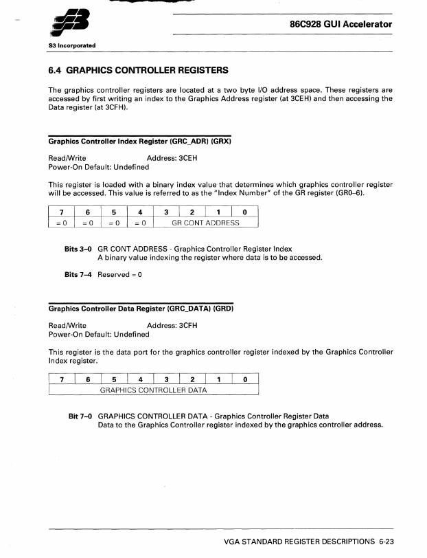
•• r 53 Incorporated
•
6.4 GRAPHICS CONTROLLER REGISTERS
86C928 GUI Accelerator
The graphics controller registers are located at a two byte I/O address space. These registers are accessed by first writing an index to the Graphics Address register (at 3CEH) and then accessing the Data register (at 3CFH).
Graphics Controller Index Register (GRC_ADR) (GRX)
Read/Write Address: 3CEH Power-On Default: Undefined
This register is loaded with a binary index value that determines which graphics controller register will be accessed. This value is referred to as the "Index Number" of the GR register (GRO-6).
320 GR CONT ADDRESS
Bits 3-0 GR CONT ADDRESS - Graphics Controller Register Index A binary value indexing the register where data is to be accessed.
Bits 7-4 Reserved = 0
Graphics Controller Data Register (GRC_DATA) (GRD)
Read/Write Address: 3CFH Power-On Default: Undefined
This register is the data port for the graphics controller register indexed by the Graphics Controller Index register.
7 6 5 432 1 o GRAPHICS CONTROLLER DATA
Bit 7-0 GRAPHICS CONTROLLER DATA - Graphics Controller Register Data Data to the Graphics Controller register indexed by the graphics controller address.
VGA STANDARD REGISTER DESCRIPTIONS 6-23
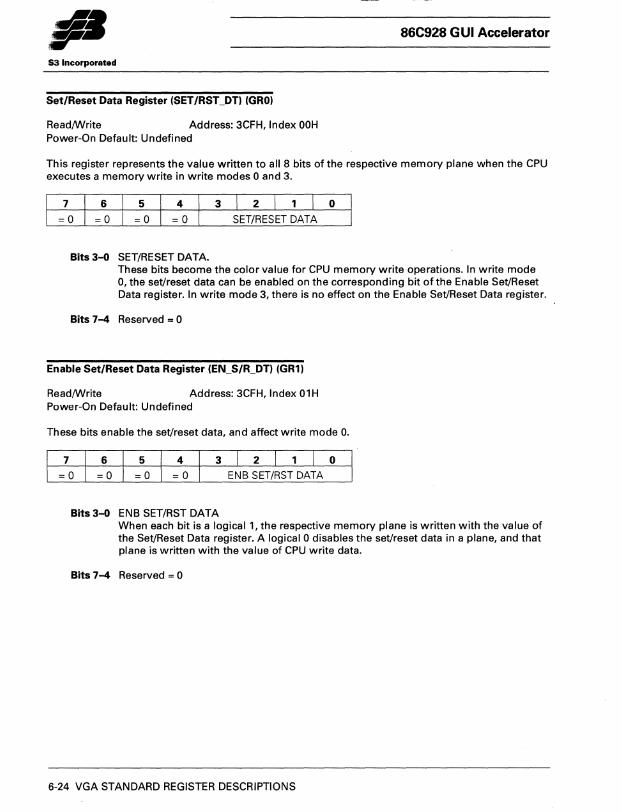
'"
86C928 GUI Accelerator
S3 Incorporated
Set/Reset Data Register (SET /RST _DT) (GRO)
ReadIWrite Address: 3CFH, Index OOH Power-On Default: Undefined
This register represents the value written to all 8 bits of the respective memory plane when the CPU executes a memory write in write modes 0 and 3.
6 4 3 2 1 o =0 =0 SET/RESET DATA
Bits 3-0 SET/RESET DATA. These bits become the color value for CPU memory write operations. In write mode 0, the set/reset data can be enabled on the corresponding bit ofthe Enable Set/Reset Data register. In write mode 3, there is no effect on the Enable Set/Reset Data register.
Bits 7-4 Reserved = 0
Enable Set/Reset Data Register (EN_S/R_DTI (GR1)
ReadIWrite Address: 3CFH, Index 01 H Power-On Default: Undefined
These bits enable the set/reset data, and affect write mode O.
3 2 0 ENB SET/RST DATA
Bits 3-0 ENBSET/RST DATA When each bit is a logical 1, the respective memory plane is written with the value of the Set/Reset Data register. A logical 0 disables the set/reset data in a plane, and that plane is written with the value of CPU write data.
Bits 7-4 Reserved = 0
6-24 VGA STANDARD REGISTER DESCRIPTIONS
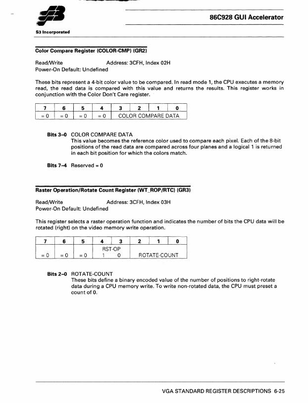
· ..
fl· 86C928 GUI Accelerator
S3 Incorporated
Color Compare Register (COLOR-CMP) (GR2)
ReadIWrite Address: 3CFH, Index 02H Power-On Default: Undefined
These bits represent a 4-bit color value to be compared. In read mode 1, the CPU executes a memory read, the read data is compared with this value and returns the results. This register works in conjunction with the Color Don't Care register.
321 0
COLOR COMPARE DATA
Bits3-O COLOR COMPARE DATA This value becomes the reference color used to compare each pixel. Each of the 8-bit positions of the read data are compared across four planes and a logical 1 is returned in each bit position for which the colors match.
Bits 7-4 Reserved = 0
Raster Operation/Rotate Count Register (WT_ROP/RTC) (GR3)
ReadIWrite Address: 3CFH, Index 03H Power-On Default: Undefined
This register selects a raster operation function and indicates the number of bits the CPU data will be rotated (right) on the video memory write operation.
7 6 5 4 I 3 2 I 1 I 0
RST-OP =0 =0 =0 1 0 ROTATE-COUNT
Bits 2-0 ROTATE-COUNT These bits define a binary encoded value of the number of positions to right-rotate data during a CPU memory write. To write non-rotated data, the CPU must preset a count of O.
VGA STANDARD REGISTER DESCRIPTIONS 6-25
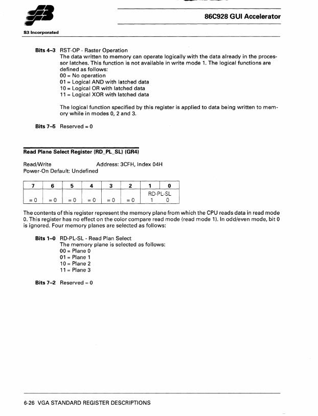
86C928 GUI Accelerator
S3 Incorporated
Bits 4-3 RST-OP - Raster Operation The data written to memory can operate logically with the data already in the processor latches. This function is not available in write mode 1. The logical functions are defined as follows: 00 = No operation 01 = Logical AND with latched data 10 = Logical OR with latched data 11 = Logical XOR with latched data
The logical function specified by this register is applied to data being written to memory while in modes 0, 2 and 3.
Bits 7-5 Reserved = 0
Read Plane Select Register (RD_PL_SL) (GR4)
ReadIWrite Address: 3CFH, Index 04H Power-On Default: Undefined
1 0
RD-PL-SL 1 0
The contents ofthis register represent the memory plane from which the CPU reads data in read mode O. This register has no effect on the color compare read mode (read mode 1). In odd/even mode, bit 0 is ignored. Four memory planes are selected as follows:
Bits 1-0 RD-PL-SL - Read Plan Select The memory plane is selected as follows: 00 = Plane 0 01 = Plane 1 10 = Plane 2 11 = Plane 3
Bits 7-2 Reserved = 0
6-26 VGA STANDARD REGISTER DESCRIPTIONS
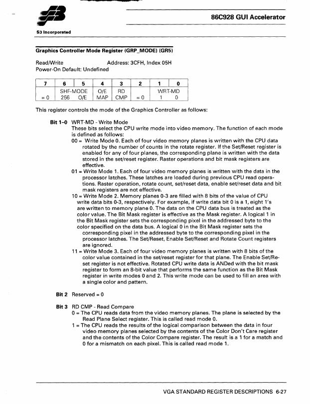
II· 86C928 GUI Accelerator
S3 Incorporated
Graphics Controller Mode Register (GRP _MODE) (GR5)
Read/Write Address: 3CFH, Index 05H Power-On Default: Undefined
7 6 1 5 4 3 2 1 I 0
SHF-MODE OlE RD WRT-MD =0 256 DIE MAP CMP =0 1 0
This register controls the mode of the Graphics Controller as follows:
Bit 1-0 WRT-MD - Write Mode These bits select the CPU write mode into video memory. The function of each mode is defined as follows: 00 = Write Mode O. Each of four video memory planes is written with the CPU data
rotated by the number of counts in the rotate register. If the Set/Reset register is enabled for any of four planes, the corresponding plane is written with the data stored in the set/reset register. Raster operations and bit mask registers are effective.
01 = Write Mode 1. Each of four video memory planes is written with the data in the processor latches. These latches are loaded during previous CPU read operations. Raster operation, rotate count, set/reset data, enable set/reset data and bit mask registers are not effective.
10 = Write Mode 2. Memory planes 0-3 are filled with 8 bits of the value of CPU write data bits 0-3, respectively. For example, if write data bit 0 is a 1, eight 1's are written to memory plane O. The data on the CPU data bus is treated as the color value. The Bit Mask register is effective as the Mask register. A logical 1 in the Bit Mask register sets the corresponding pixel in the addressed byte to the color specified on the data bus. A logical 0 in the Bit Mask register sets the
corresponding pixel in the addressed byte to the corresponding pixel in the processor latches. The Set/Reset, Enable Set/Reset and Rotate Count registers are ignored.
11 = Write Mode 3. Each of four video memory planes is written with 8 bits of the color value contained in the set/reset register for that plane. The Enable Set/Reset register is not effective. Rotated CPU write data is ANDed with the bit mask register to form an 8-bit value that performs the same function as the Bit Mask register in write modes 0 and 2. This write mode can be used to fill an area with a single color and pattern.
Bit 2 Reserved = 0
Bit 3 RD CMP - Read Compare 0= The CPU reads data from the video memory planes. The plane is selected by the
Read Plane Select register. This is called read mode O. 1 = The CPU reads the results of the logical comparison between the data in four
video memory planes selected by the contents of the Color Don't Care register and the contents of the Color Compare register. The result is a 1 for a match and o for a mismatch on each pixel. This is called read mode 1.
VGA STANDARD REGISTER DESCRIPTIONS 6-27
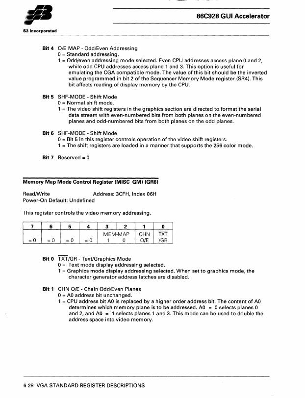
86C928 GUI Accelerator
S3 Incorporated
Bit 4 OlE MAP - Odd/Even Addressing 0= Standard addressing. 1 = Odd/even addressing mode selected. Even CPU addresses access plane 0 and 2,
while odd CPU addresses access plane 1 and 3. This option is useful for emulating the CGA compatible mode. The value of this bit should be the inverted value programmed in bit 2 ofthe Sequencer Memory Mode register (SR4). This bit affects reading of display memory by the CPU.
Bit 5 SHF-MODE - Shift Mode 0= Normal shift mode. 1 = The video shift registers in the graphics section are directed to format the serial
data stream with even-numbered bits from both planes on the even-numbered planes and odd-numbered bits from both planes on the odd planes.
Bit 6 SHF-MODE - Shift Mode 0= Bit 5 in this register controls operation of the video shift registers. 1 = The shift registers are loaded in a manner that supports the 256 color mode.
Bit 7 Reserved = 0
Memory Map Mode Control Register (MISC_GM) (GR6)
ReadIWrite Address: 3CFH, Index 06H Power-On Default: Undefined
This register controls the video memory addressing.
7
=0
6 5 4 3 I 2 1 0
MEM-MAP CHN TXT =0 =0 =0 1 0 OlE /GR
Bit 0 TXT/GR - Text/Graphics Mode o = Text mode display addressing selected. 1 = Graphics mode display addressing selected. When set to graphics mode, the
character generator address latches are disabled.
Bit 1 CHN OlE - Chain Odd!Even Planes 0= AO address bit unchanged. 1 = CPU address bit AO is replaced by a higher order address bit. The content of AO
determines which memory plane is to be addressed. AO = 0 selects planes 0 and 2, and AO = 1 selects planes 1 and 3. This mode can be used to double the address space into video memory.
6-28 VGA STANDARD REGISTER DESCRIPTIONS
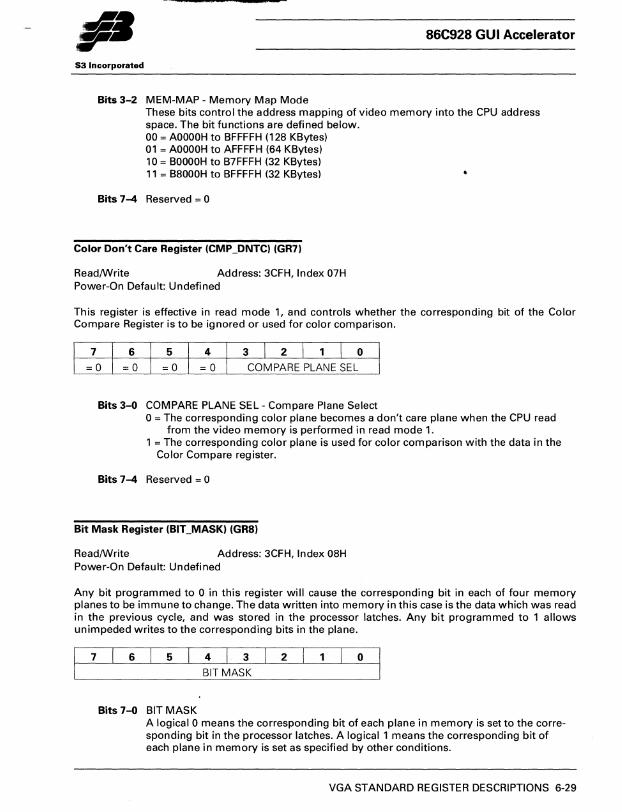
86C928 GUI Accelerator
53 Incorporated
Bits 3-2 MEM-MAP - Memory Map Mode These bits control the address mapping of video memory into the CPU address space. The bit functions are defined below. 00 = AOOOOH to BFFFFH (128 KBytes) 01 = AOOOOH to AFFFFH (64 KBytes) 10 = BOOOOH to B7FFFH (32 KBytes) 11 = B8000H to BFFFFH (32 KBytes)
Bits 7-4 Reserved = 0
Color Don't Care Register (CMP _DNTC) (GR7)
Read/Write Address: 3CFH, Index 07H Power-On Default: Undefined
This register is effective in read mode 1, and controls whether the corresponding bit of the Color Compare Register is to be ignored or used for color comparison.
3 2 o COMPARE PLANE SEL
Bits 3-0 COMPARE PLANE SEL - Compare Plane Select 0= The corresponding color plane becomes a don't care plane when the CPU read
from the video memory is performed in read mode 1. 1 = The corresponding color plane is used for color comparison with the data in the
Color Compare register.
Bits 7-4 Reserved = 0
Bit Mask Register (BIT_MASK) (GR8)
Read/Write Address: 3CFH, Index 08H Power-On Default: Undefined
Any bit programmed to 0 in this register will cause the corresponding bit in each of four memory planes to be immune to change. The data written into memory in this case is the data which was read in the previous cycle, and was stored in the processor latches. Any bit programmed to 1 allows unimpeded writes to the corresponding bits in the plane.
7 6 5 4 3 2 o BIT MASK
Bits 7-0 BIT MASK A logical 0 means the corresponding bit of each plane in memory is set to the corresponding bit in the processor latches. A logical 1 means the corresponding bit of each plane in memory is set as specified by other conditions.
VGA STANDARD REGISTER DESCRIPTIONS 6-29
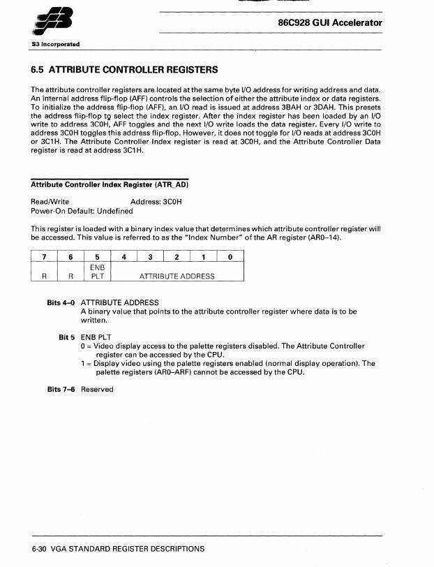
86C928 GUI Accelerator
S3 Incorporated
6.5 ATTRIBUTE CONTROLLER REGISTERS
The attribute controller registers are located at the same byte I/O address for writing address and data. An internal address flip-flop (AFF) controls the selection of either the attribute index or data registers. To initialize the address flip-flop (AFF), an I/O read is issued at address 3BAH or 3DAH. This presets the address flip-flop t<;l select the index register. After the index register has been loaded by an I/O write to address 3COH, AFF toggles and the next I/O write loads the data register. Every I/O write to address 3COH toggles this address flip-flop. However, it does not toggle for I/O reads at address 3COH or 3C1 H. The Attribute Controller Index register is read at 3COH, and the Attribute Controller Data register is read at address 3C1 H.
Attribute Controller Index Register (ATR_AO)
ReadIWrite Address: 3COH Power-On Default: Undefined
Th is register is loaded with a bi nary index value that determ ines which attribute controller register will be accessed. This value is referred to as the "Index Number" of the AR register (ARO-14).
7
R
6 5 4 I 3 I 2 I 1 I 0
ENB R PLT ATTRIBUTE ADDRESS
Bits 4-0 ATTRIBUTE ADDRESS A binary value that points to the attribute controller register where data is to be written.
Bit 5 ENB PLT 0= Video display access to the palette registers disabled. The Attribute Controller
register can be accessed by the CPU. 1 = Display video using the palette registers enabled (normal display operation). The
palette registers (ARO-ARF) cannot be accessed by the CPU.
Bits 7-6 Reserved
6-30 VGA STANDARD REGISTER DESCRIPTIONS
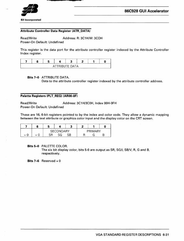
86C928 GUI Accelerator
53 In corporated
Attribute Controller Data Register IATR_DATA)
ReadIWrite Address: R: 3C1H/W: 3COH Power-On Default: Undefined
This register is the data port for the attribute controller register indexed by the Attribute Controller Index register.
7 6 5 432 o ATTRIBUTE DATA
Bits 7-0 ATTRIBUTE DATA. Data to the attribute controller register indexed by the attribute controller address.
Palette Registers IPLT_REG) IAROO-OF)
Read/Write Address: 3C1 H/3COH, Index OOH-OFH Power-On Default: Undefined
These are 16, 6-bit registers pointed to by the index and color code. They allow a dynamic mapping between the text attribute or graphics color input and the display color on the CRT screen.
7 6 5 I 4 I 3 2 I 1 I 0
SECONDARY PRIMARY =0 =0 SR SG SB R G B
Bits 5-0 PALETTE COLOR. The six bit display color, bits 5-0 are output as SR, SG/I, SB/V, R, G and B, respectively.
Bits 7-6 Reserved = 0
VGA STANDARD REGISTER DESCRIPTIONS 6-31
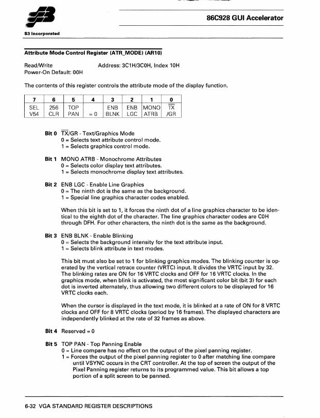
•• r 86C928 GUI Accelerator
53 Incorporated
Attribute Mode Control Register (ATR_MODE) (AR10)
Read/Write Address: 3C1 H/3COH, Index 10H Power-On Default: OOH
The contents of this register controls the attribute mode of the display function.
7
SEL V54
6 5 4 3 2 1 0
256 TOP ENB ENB MONO TX CLR PAN =0 BLNK LGC ATRB /GR
Bit 0 TX/GR - Text/Graphics Mode 0= Selects text attribute control mode. 1 = Selects graphics control mode.
Bit 1 MONO ATRB - Monochrome Attributes 0= Selects color display text attributes. 1 = Selects monochrome display text attributes.
Bit 2 ENB LGC - Enable Line Graphics 0= The ninth dot is the same as the background. 1 = Special line graphics character codes enabled.
When this bit is set to 1, it forces the ninth dot of a line graphics character to be identical to the eighth dot of the character. The line graphics character codes are COH through DFH. For other characters, the ninth dot is the same as the background.
Bit 3 ENB BLNK - Enable Blinking 0= Selects the background intensity for the text attribute input. 1 = Selects blink attribute in text modes.
This bit must also be set to 1 for blinking graphics modes. The blinking counter is operated by the vertical retrace counter (VRTC) input. It divides the VRTC input by 32. The blinking rates are ON for 16 VRTC clocks and OFF for 16 VRTC clocks. In the graphics mode, when blink is activated, the most significant color bit (bit 3) for each dot is inverted alternately, th us allowing two different colors to be displayed for 16 VRTC clocks each.
When the cursor is displayed in the text mode, it is blinked at a rate of ON for 8 VRTC clocks and OFF for 8 VRTC clocks (period by 16 frames). The displayed characters are independently blinked at the rate of 32 frames as above.
Bit 4 Reserved = 0
Bit 5 TOP PAN - Top Panning Enable 0= Line compare has no effect on the output of the pixel panning register. 1 = Forces the output of the pixel panning register to 0 after matching line compare
until VSYNC occurs in the CRT controller. At the top of screen the output of the Pixel Panning register returns to its programmed value. This bit allows a top portion of a split screen to be panned.
6-32 VGA STANDARD REGISTER DESCRIPTIONS
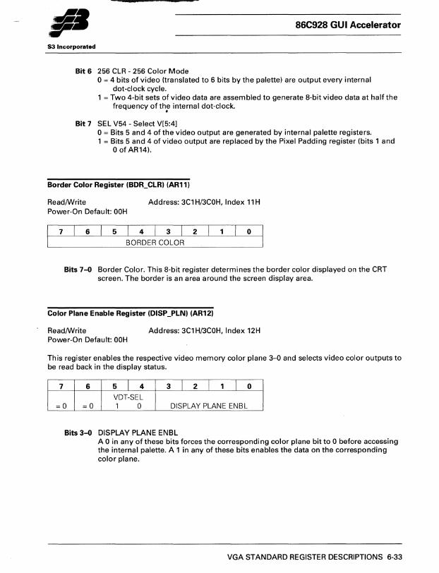
86C928 GUI Accelerator
53 Incorporatad
Bit 6 256 CLR - 256 Color Mode 0= 4 bits of video (translated to 6 bits by the palette) are output every internal
dot-clock cycle. 1 = Two 4-bit sets of video data are assembled to generate 8-bit video data at half the
frequency ofth; internal dot-clock.
Bit 7 SEL V54 - Select V[5:4] 0= Bits 5 and 4 of the video output are generated by internal palette registers. 1 = Bits 5 and 4 of video output are replaced by the Pixel Padding register (bits 1 and
o of AR14).
Border Color Register (BDR_CLR) (AR11)
Read/Write Address: 3C1 H/3COH, Index 11 H Power-On Default: OOH
7 6 5 4 3 2 o BORDER COLOR
Bits 7-0 Border Color. This 8-bit register determines the border color displayed on the CRT screen. The border is an area around the screen display area.
Color Plane Enable Register (DISP_PLN) (AR12)
Read/Write Address: 3C1 H/3COH, Index 12H Power-On Default: OOH
This register enables the respective video memory color plane 3-0 and selects video color outputs to be read back in the display status.
7 6 5 I 4 3 I 2 I 1 I 0 VDT-SEL
=0 =0 1 0 DISPLAY PLANE ENBL
Bits 3-0 DISPLAY PLANE ENBL A 0 in any of these bits forces the correspondi ng color plane bit to 0 before accessing the internal palette. A 1 in any of these bits enables the data on the corresponding color plane.
VGA STANDARD REGISTER DESCRIPTIONS 6-33
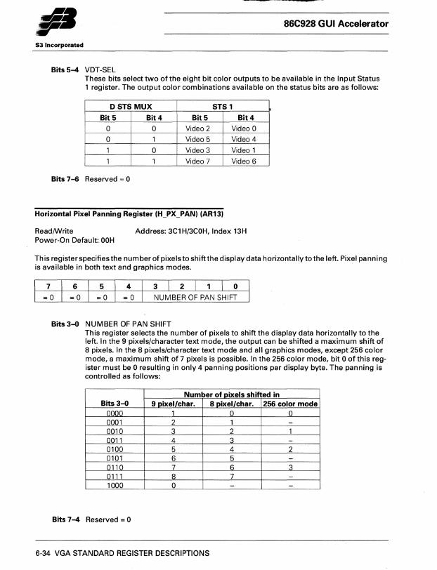
86C928 GUI Accelerator
53 Incorporated
Bits 5-4 VDT-SEL These bits select two of the eight bit color outputs to be available in the Input Status 1 register. The output color combinations available on the status bits are as follows:
D STS MUX STS 1
Bit 5 Bit4 Bit 5 Bit4
0 0 Video 2 Video 0 0 1 Video 5 Video 4
1 0 Video 3 Video 1 1 1 Video 7 Video 6
Bits 7-6 Reserved = 0
Horizontal Pixel Panning Register (H_PX_PAN) (AR13)
ReadIWrite Address: 3C1 H/3COH, Index 13H Power-On Default: OOH
This register specifies the number of pixelsto shiftthe display data horizontally tothe left. Pixel panning is available in both text and graphics modes.
6 321 0 =0 NUMBER OF PAN SHIFT
Bits 3-0 NUMBER OF PAN SHIFT This register selects the number of pixels to shift the display data horizontally to the left. In the 9 pixels/character text mode, the output can be shifted a maximum shift of 8 pixels. In the 8 pixels/character text mode and all graphics modes, except 256 color mode, a maximum shift of 7 pixels is possible. In the 256 color mode, bit 0 of this register must be 0 resulting in only 4 panning positions per display byte. The panning is controlled as follows:
Number of pixels shifted in Bits 3-0 9 pixel/char. S pixel/char. 256 color mode
0000 1 0 0 0001 2 1 -0010 3 2 1 0011 4 3 -0100 5 4 2 0101 6 5 -0110 7 6 3 0111 8 7 -1000 0 - -
Bits 7-4 Reserved = 0
6-34 VGA STANDARD REGISTER DESCRIPTIONS
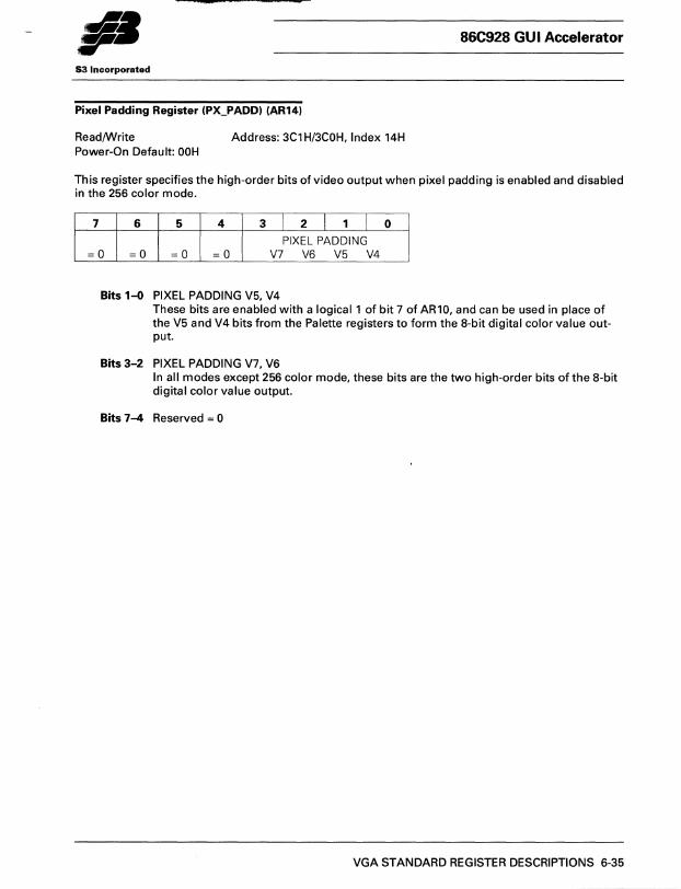
-II· 86C928 GUI Accelerator
S3 Incorporated
Pixel Padding Register (PX_PADD) (AR14)
ReadIWrite Address: 3C1 H/3COH, Index 14H Power-On Default: OOH
Th is register specifies the high-order bits of video output when pixel padding is enabled and disabled in the 256 color mode.
7 6 5 4 3 I 2 I 1 I 0
PIXEL PADDING =0 =0 =0 =0 V7 V6 V5 V4
Bits 1-0 PIXEL PADDING V5, V4 These bits are enabled with a logical 1 of bit 7 of AR10, and can be used in place of the V5 and V4 bits from the Palette registers to form the 8-bit digital color value output.
Bits 3-2 PIXEL PADDING V7, V6 In all modes except 256 color mode, these bits are the two high-order bits ofthe 8-bit digital color value output.
Bits 7-4 Reserved = 0
VGA STANDARD REGISTER DESCRIPTIONS 6-35
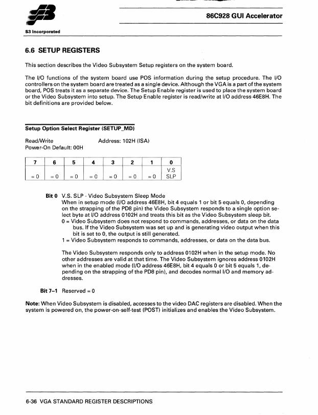
=
86C928 GUI Accelerator
53 Incorporated
6.6 SETUP REGISTERS
This section describes the Video Subsystem Setup registers on the system board.
The I/O functions of the system board use POS information during the setup procedure. The I/O controllers on the system board are treated as a single device. Although the VGA is a part of the system board, POS treats it as a separate device. The Setup Enable register is used to place the system board or the Video Subsystem into setup. The Setup Enable register is read/write at I/O address 46E8H. The bit definitions are provided below.
Setup Option Select Register (SETUP _MO)
Read/Write Address: 102H (lSA) Power-On Default: OOH
Bit 0 V.S. SLP - Video Subsystem Sleep Mode When in setup mode (I/O address 46E8H, bit 4 equals 1 or bit 5 equals 0, depending on the strapping of the PD8 pin) the Video Subsystem responds to a single option select byte at I/O address 0102H and treats this bit as the Video Subsystem sleep bit. 0= Video Subsystem does not respond to commands, addresses, or data on the data
bus. If the Video Subsystem was set up and is generating video output when this bit is set to 0, the output is still generated.
1 = Video Subsystem responds to commands, addresses, or data on the data bus.
The Video Subsystem responds only to address 0102H when in the setup mode. No other addresses are valid at that time. The Video Subsystem ignores address 0102H when in the enabled mode (1/0 address 46E8H, bit 4 equals 0 or bit 5 equals 1, depending on the strapping of the PD8 pin), and decodes normal 1/0 and memory addresses.
Bit 7-1 Reserved = 0
Note: When Video Subsystem is disabled, accesses to the video DAC registers are disabled. When the system is powered on, the power-on-self-test (POST) initializes and enables the Video Subsystem.
6-36 VGA STANDARD REGISTER DESCRIPTIONS
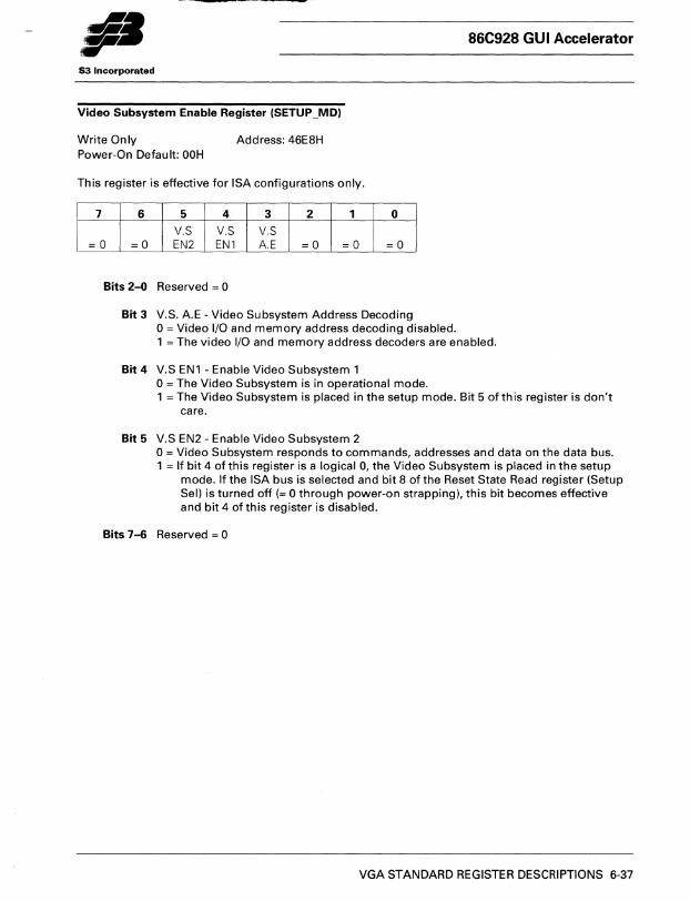
86C928 GUI Accelerator
S3 Incorporated
Video Subsystem Enable Register (SETUP_MOl
Write Only Address: 46E8H Power-On Default: OOH
This register is effective for ISA configurations only.
Bits 2-0 Reserved = 0
Bit 3 V.S. A.E - Video Subsystem Address Decoding 0= Video I/O and memory address decoding disabled. 1 = The video I/O and memory address decoders are enabled.
Bit 4 V.S EN1 - Enable Video Subsystem 1 o = The Video Subsystem is in operational mode. 1 = The Video Subsystem is placed in the setup mode. Bit 5 of this register is don't
care.
Bit 5 V.S EN2 - Enable Video Subsystem 2 0= Video Subsystem responds to commands, addresses and data on the data bus. 1 = If bit 4 of this register is a logical 0, the Video Subsystem is placed in the setup
mode. If the ISA bus is selected and bit 8 of the Reset State Read register (Setup Sel) is turned off (= 0 through power-on strapping), this bit becomes effective and bit 4 of this register is disabled.
Bits 7-6 Reserved = 0
VGA STANDARD REGISTER DESCRIPTIONS 6-37
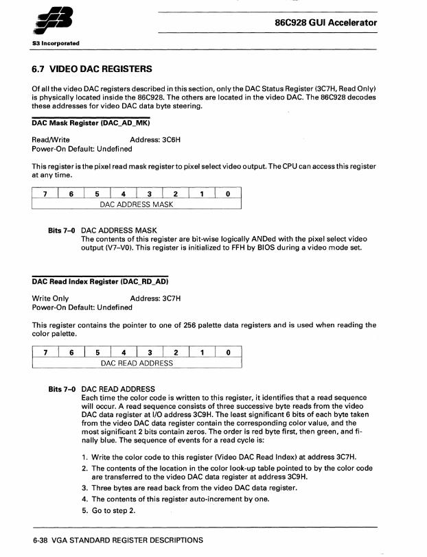
II· 86C928 GUI Accelerator
S3 Incorporated
6.7 VIDEO DAC REGISTERS
Of all the video DAC registers described in this section, only the DAC Status Register (3C7H, Read Only) is physically located inside the 86C928. The others are located in the video DAC. The 86C928 decodes these addresses for video DAC data byte steering.
DAC Mask Register {DAC_AD_MKI
Read/Write Address: 3C6H Power-On Default: Undefined
This register is the pixel read mask register to pixel select video output. The CPU can access this register at anytime.
7 6 543 2 o DAC ADDRESS MASK
Bits 7-0 DAC ADDRESS MASK The contents of this register are bit-wise logically ANDed with the pixel select video output (V7-VO). This register is initialized to FFH by BIOS during a video mode set.
DAC Read Index Register {DAC_RD_ADI
Write Only Address: 3C7H Power-On Default: Undefined
This register contains the pointer to one of 256 palette data registers and is used when reading the color palette.
7 6 5 4 3 2 o DAC READ ADDRESS
Bits 7-0 DAC READ ADDRESS Each time the color code is written to this register, it identifies that a read sequence will occur. A read sequence consists of three successive byte reads from the video DAC data register at I/O address 3C9H. The least significant 6 bits of each byte taken from the video DAC data register contain the corresponding color value, and the most significant 2 bits contain zeros. The order is red byte first, then green, and finally blue. The sequence of events for a read cycle is:
1. Write the color code to this register (Video DAC Read Index) at address 3C7H.
2. The contents of the location in the color look-up table pointed to by the color code are transferred to the video DAC data register at address 3C9H.
3. Three bytes are read back from the video DAC data register.
4. The contents of this register auto-increment by one.
5. Go to step 2.
6-38 VGA STANDARD REGISTER DESCRIPTIONS
S3 Incorporated
86C928 GUI Accelerator
If this register is written to during either a read or write cycle, a mode is initialized and the unfinished cycle is aborted. The effects of writing to the video DAC data register during a read cycle or reading from the video DAC data register during a write cycle are undefined and may change the look-up table contents.
DAC Status Register (DAC_STS)
Read Only Address: 3C7H Power-On Default: Undefined
3 2 1 0
=0 =0
Bits 1-0 DAC-STS - Video DAC Cycle Status The last executing cycle was: 00 = Write Palette cycle 11 = Read Palette cycle
DAC-STS
Reads from the Video DAC Write Index at address 3C8H or the DAC status register at address 3C7H do not interfere with read or write cycles and may take place at any time.
Bits 7-2 Reserved = 0
DAC Write Index Register (OAC_WR_AO)
ReadIWrite Address: 3C8H Power-On Default: Undefined
Bits 7-0 DAC WRITE ADDRESS/GIP READ DATA This register contains the pointer to one of 256 palette data registers and is used during a palette load. Each time the color code is written to this register, it identifies that a write sequence will occur. A write sequence consists of three successive byte writes to the DAC data register at I/O address 3C9H. The least significant 6 bits of each byte are concatenated to form the value placed in the 18-bit data register. The order is red byte first, then green, and finally blue. Once the third byte has been written, the value in the data register is written to the location pointed to by the color code. The sequence of events for a write cycle is:
VGA STANDARD REGISTER DESCRIPTIONS 6-39
53 Incorporated
86C928 GUI Accelerator
1. Write the color code to this register (DAC Write Index) at address 3C8H.
2. Three bytes are written to the DAC Data register at address 3C9H.
3. The contents of the DAC data register are transferred to the location in the color look-up table pointed to by the color code.
4. The DAC Write Index register auto-increments by 1.
5. Go to step 2.
If bit 2 of the Extended Video DAC Control register (3?5H, Index 55H) is set to 1 to enable the General I/O Port read function, a read of 3C8H retrieves data from an external input buffer.
Video DAC Data Register (DAC_DATA)
Read/Write Address: 3C9H Power-On Default: Undefined
This register is a data port to read or write the contents ofthe location in the color look-up table pointed to by the DAC Read Index or the DAC Write Index registers.
7 6 5 4 3 2 o DAC READ/WRITE DATA
Bits 7-0 DAC READ/WRITE DATA To prevent "snow flicker" on the screen, an application reading data from or writing data to the DAC Data register should ensure that the BLANK input to the video DAC is asserted. This can be accomplished either by restricting data transfers to retrace intervals, checking the Input Status 1 register to determine when retrace is occurring, or by using the screen-off bit in the Clocking Mode register of the sequencer.
6-40 VGA STANDARD REGISTER DESCRIPTIONS
II· 86C928 GUI Accelerator.
S3 Incorporated
Section 7: S3 VGA Register Descriptions
The 86C928 has additional registers to extend the functions of basic VGA. These registers are located in CRT Controller address space at locations not used by IBM. All of these registers are read/write protected at power-up by hardware reset. In order to read/write these registers, the Register Lock 1 register (CR38) must be loaded with a binary unlock key pattern (see the register description). The registers will remain unlocked until the key pattern is reset by altering a significant bit.
In the following register descriptions, 'U' stands for undefined or unused and 'R' stands for reserved (write =0, read = U). See Appendix A for a table listing each register in this section and its page number.
Chip ID/REV Register (CHIP-ID/REV) (CR30)
Read Only Address: 3?5H, Index 30H Power-On Default: 90H
7 6 5 4 3 2 1 0
CHIP ID REVISION STATUS
Bits 7-0 CHIP 10 AND REVISION STATUS
Memory Configuration Register (MEM_CNFG) (CR31)
Read/Write Address: 3?5H, Index 31 H Power-On Default: OOH
7 6 5 I 4 3 2 1 0 EXT HST STRT-ADR ENH VGA SCRN CPUA
BIOS OFF 17 16 MAP 16B 2.PG BASE
Bit 0 CPUA BASE - Enable Base Address Offset 0= Address offset bits 3-0 of the CRT Register Lock register and bit 2 of the
Extended System Control 2 register are disabled. 1 = Address offset bits 3-0 ofthe CRT Register Lock register and bit 2 ofthe
Extended System Control 2 register are enabled for whole VGA display memory access by the CPU.
S3 VGA REGISTER DESCRIPTIONS 7-1
86C928 GUI Accelerator
S3 Incorporated
Bit 1 SCRN 2.PG - Two-Page Screen Image 0= Normal Mode 1 = Enable 2K x 1 K x 4 map image screen for 1024 x 768 or 800 x 600 screen
resolution, or 2K x 512 x 8 map image screen for 640 x 480 screen resolution.
Bit 2 VGA 16B - VGA 16-bit Memory Bus Width o = 8-bit memory bus operation 1 = Enable 16-bit bus VGA memory read/writes
Bit 3 ENH MAP - Enhanced Memory Mapping o = Forces IBM VGA mapping for memory accesses. 1 = Forces Enhanced Mode mappings.
Bits 5-4 STRT-ADR 17,16 - Start Address Bits 17-16 Bits 17-16 of start address, cursor location, and font access address registers
Note: Bit 2 of the Extended System Control 2 register (CR51) is bit 18 of the address and enables access to up to 2 MBytes of display memory.
Bit 6 HST OFF - High Speed Text Display Font Fetch Mode o = Normal Font Access Mode 1 = Enable Page Mode for Alpha Mode Font Access
Bit 7 EXT BIOS - External BIOS ROM Space (C6000H-C67FFH) Mapping 0= External BIOS ROM space is not readable (default). 1 = External BIOS ROM space is readable.
Note: If power-on strapping bit PD3 = 1, the setting of this bit has no effect and all 32 KBytes of BIOS ROM are available.
Backward Compatibility 1 Register (BKWD_11 (CR321
Read/Write Address: 3?5H, Index 32H Power-On Default: OOH
7 6 5 4 3 2 1 I 0
SRO- VGA EGA EGA BKWD FCHI CH-CLK TRI FXPG (R) (R) MODE CHCK 1 0
Bits 1-0 CH-CLK - Character Clock Period 00 = Same as IBM VGA (8 or 9 dot clocks) 01 = 7 dots (used for 132 character mode) 10 = 9 dots 11 = Reserved
Bit 2 FCHI CHCK - Force Character Clock High 0= Normal character clock 1 = Force character clock of horizontal timing to high rate (not 1/2 dot clock rate) for
CGA and HGC emulations.
7-2 S3 VGA REGISTER DESCRIPTIONS
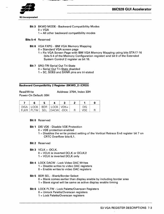
#
86C928 GUI Accelerator
53 Incorporated
Bit 3 BKWD MODE - Backward Compatibility Modes O=VGA 1 = All other backward compatibility modes
Bits 5-4 Reserved
Bit 6 VGA FXPG - IBM VGA Memory Mapping o = Standard VGA screen page 1 = Fix VGA Screen Page with IBM VGA Memory Mapping using bits STA17-16
(bits 5-4 of the Memory Configuration register) and bit 0 of the Extended System Control 2 register as bit 18.
Bit 7 SRO-TRI Serial Out Tri-State 0= Serial Out Tri-State disabled -- --1 = SC, SOEO and SXNR pins are tri-stated
Backward Compatibility 2 Register (BKWD_2) (CR33)
Read/Write Address: 3?5H, Index 33H Power-On Default: OOH
7
DISA FLKR
6 5 4 3 2
LOCK BDR LOCK VDK= PLTW SEL DACW -DCK R
Bit 0 Reserved
Bit 1 DIS VDE - Disable VDE Protection 0= VDE protection enabled
1 0
DIS VDE R
1 = Disables the write protect setting of the Vertical Retrace End register bit 7 on CRTC Overflow bits 6,1.
Bit 2 Reserved
Bit 3 VCLK = -DCLK. 0= VCLK is inverted DCLK or DCLK/2 1 = VCLK is inverted DCLK only
Bit 4 LOCK DACW - Lock Video DAC Writes 1 = Disable writes to video DAC registers o = Enable writes to video DAC registers
Bit 5 BDR SEL - Blank/Border Select 0= Blank comes earlier than display enable by including border area 1 = Blank signal will be same as active display enable timing
Bit 6 LOCK PL TW - Lock Palette/Overscan Registers 0= Unlock Palette/Overscan registers 1 = Lock Palette/Overscan registers
S3 VGA REGISTER DESCRIPTIONS 7-3
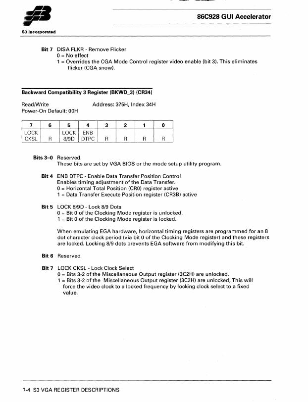
II· 86C928 GUI Accelerator
53 Incorporated
Bit 7 DISA FLKR - Remove Flicker 0= No effect 1 = Overrides the CGA Mode Control register video enable (bit 3). This eliminates
flicker (CGA snow).
Backward Compatibility 3 Register (BKWD_3) (CR34)
ReadIWrite Address: 3?5H, Index 34H Power-On Default: OOH
7 6 5 4 3 2 1 0
LOCK LOCK ENB CKSL R 8/9D DTPC R R R R
Bits 3-0 Reserved. These bits are set by VGA BIOS or the mode setup utility program.
Bit 4 ENB DTPC - Enable Data Transfer Position Control Enables timing adjustment of the Data Transfer. 0= Horizontal Total Position (CRO) register active 1 = Data Transfer Execute Position register (CR3B) active
Bit 5 LOCK 8/9D - Lock 8/9 Dots 0= Bit 0 of the Clocking Mode register is unlocked. 1 = Bit 0 of the Clocking Mode register is locked.
When emulating EGA hardware, horizontal timing registers are programmed for an 8 dot character clock period (via bit 0 of the Clocking Mode register) and these registers are locked. Locking 8/9 dots prevents EGA software from modifying this bit.
Bit 6 Reserved
Bit 7 LOCK CKSL - Lock Clock Select 0= Bits 3-2 ofthe Miscellaneous Output register (3C2H) are unlocked. 1 = Bits 3-2 ofthe Miscellaneous Output register (3C2H) are unlocked, This will
force the video clock to a locked frequency by locking clock select to a fixed value.
7-4 S3 VGA REGISTER DESCRIPTIONS
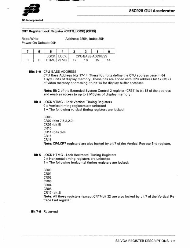
• -86C928 GUI Accelerator
53 Incorporated
CRT Register Lock Register (CRTR_LOCK) (CR35)
Read/Write Address: 3?5H, Index 35H Power-On Default: OOH
7
R
6 5 4 3 I 2 I 1 I 0
LOCK LOCK CPU-BASE-ADDRESS R HTMG VTMG 17 16 15 14
Bits 3-0 CPU-BASE-ADDRESS CPU Base Address bits 17-14. These four bits define the CPU address base in 64 KByte units of display memory. These bits are added with CPU address bit 17 (MSB of video memory addressing) to bit 14 for display buffer accesses.
Note: Bit 2 of the Extended System Control 2 register (CR51) is bit 18 of the address and enables access to up to 2 MBytes of display memory.
Bit 4 LOCK VTMG - Lock Vertical Timing Registers 0= Vertical timing registers are unlocked 1 = The following vertical timing registers are locked:
CR06 CR07 (bits 7,5,3,2,0) CR09 (bit 5) CR10 CR 11 (bits 3-0) CR15 CR16 Note: CR6,CR7 registers are also locked by bit 7 of the Vertical Retrace End register.
Bit 5 LOCK HTMG - Lock Horizontal Timing Registers 0= Horizontal timing registers are unlocked 1 = The following horizontal timing registers are locked:
CROO CR01 CR02 CR03 CR04 CR05 CR17 (bit 2) Note: All these registers (except CR17(bit 2» are also locked by bit 7 of the Vertical Retrace End register.
Bit 7-6 Reserved
S3 VGA REGISTER DESCRIPTIONS 7-5
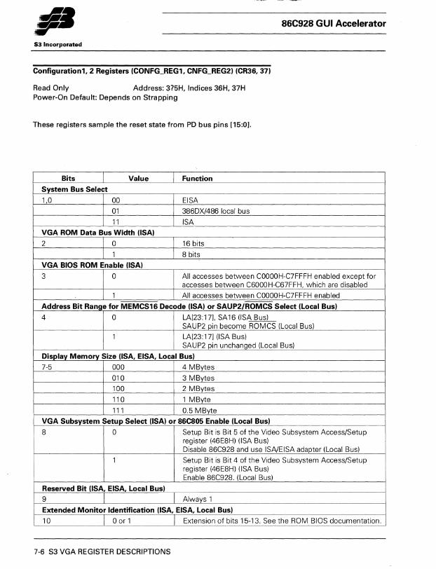
-.. ~ ,. 53 Incorporated
-86C928 GUI Accelerator
Configuration1,2 Registers (CONFG_REG1, CNFG_REG2) (eR36, 37)
Read Only Address: 3?5H, Indices 36H, 37H Power-On Default: Depends on Strapping
These registers sample the reset state from PD bus pins [15:0].
'.
Bits Value Function
System Bus Select
1,0 00 EISA
01 386DX/486 local bus
11 ISA
VGA ROM Data Bus Width liSA)
2 0 16 bits
1 8 bits VGA BIOS ROM Enable liSA)
3 0 All accesses between COOOOH-C7FFFH enabled except for accesses between C6000H-C67FFH, which are disabled
1 All accesses between COOOOH-C7FFFH enabled
Address Bit Range for MEMCS16 Decode liSA) or SAUP2/ROMCS Select (Local Bus)
4 0 LA[23:171. SA16 (lS~ SAUP2 pin become ROMCS (Local Bus)
1 LA[23: 17] (lSA Bus) SAUP2 pin unchanged (Local Bus)
Display Memory Size liSA, EISA, Local Bus)
7-5 000 4 MBytes
010 3 MBytes
100 2 MBytes
110 1 MByte
111 0.5 MByte
VGA Subsystem Setup Select liSA) or 86C805 Enable (Local Bus)
8 0 Setup Bit is Bit 5 of the Video Subsystem Access/Setup register (46E8H) (ISA Bus) Disable 86C928 and use ISA/EISA adapter (Local Bus)
1 Setup Bit is Bit 4 of the Video Subsystem Access/Setup register (46E8H) (ISA Bus) Enable 86C928. (Local Bus)
Reserved Bit liSA, EISA, Local Bus)
9 Always 1
Extended Monitor Identification liSA, EISA, Local Bus)
10 o or 1 Extension of bits 15-13. See the ROM BIOS documentation.
7-6 S3 VGA REGISTER DESCRIPTIONS
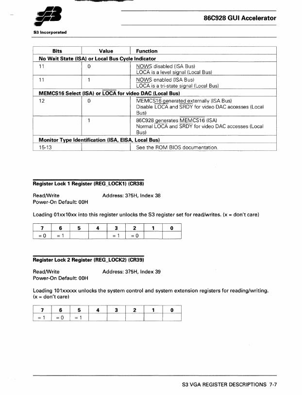
&2 ......
86C928 GUI Accelerator
53 Incorporated
Bits Value Function
No Wait State (lSA) or Local Bus Cycle Indicator
11 0 NOWS disabled (ISA Bus) LOCA is a level signal (Local Bus)
11 1 NOWS enabled (ISA Bus) LOCA is a tri-state signal (Local Bus)
MEMCS16 Select (lSA) or LOCA for video DAC (Local Bus)
12 0 MEMCS16 generated externally (lSA Bus) Disable LOCA and SRDY for video DAC accesses (Local Bus)
1 86C928 generates MEMCS16 (lSA) Normal LOCA and SRDY for video DAC accesses (Local Bus)
Monitor Type Identification (lSA, EISA, Local Bus)
15-13 See the ROM BIOS documentation.
Register Lock 1 Register (REG_LOCK1) (CR3S)
Read/Write Address: 3?5H, Index 38 Power-On Default: OOH
Loading 01xx10xx into this register unlocks the S3 register set for read/writes. (x = don't care)
5 4 o
Register Lock 2 Register (REG_LOCK2) (CR39)
Read/Write Address: 3?5H, Index 39 Power-On Default: OOH
Loading 101xxxxx unlocks the system control and system extension registers for reading/writing. (x = don't care)
4 3 2 o
53 VGA REGISTER DESCRIPTIONS 7-7
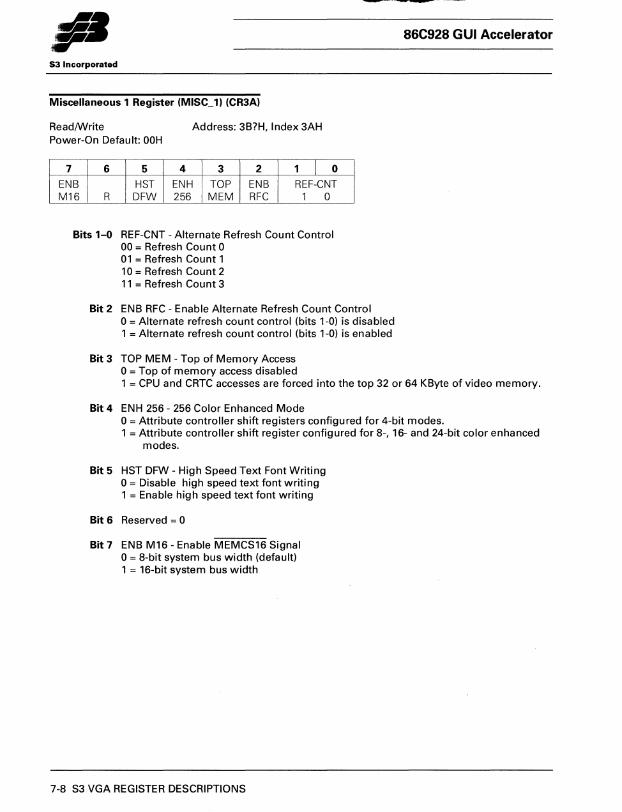
~ --II. 86C928 GUI Accelerator
53 Incorporated
Miscellaneous 1 Register (MISC_1) (CR3A)
Read/Write Address: 3B?H, Index 3AH Power-On Default: DOH
7 6 5 4 3 2 1 I 0
ENB HST ENH TOP ENB REF-CNT M16 R DFW 256 MEM RFC 1 0
Bits 1-0 REF-CNT - Alternate Refresh Count Control 00 = Refresh Count 0 01 = Refresh Count 1 10= Refresh Count 2 11 = Refresh Count 3
Bit 2 ENB RFC - Enable Alternate Refresh Count Control 0= Alternate refresh count control (bits 1-0) is disabled 1 = Alternate refresh count control (bits 1-0) is enabled
Bit 3 TOP MEM - Top of Memory Access 0= Top of memory access disabled 1 = CPU and CRTC accesses are forced into the top 32 or 64 KByte of video memory.
Bit 4 ENH 256 - 256 Color Enhanced Mode 0= Attribute controller shift registers configured for 4-bit modes. 1 = Attribute controller shift register configured for 8-,16- and 24-bit color enhanced
modes.
Bit 5 HST DFW - High Speed Text Font Writing 0= Disable high speed text font writing 1 = Enable high speed text font writing
Bit 6 Reserved = 0
Bit 7 ENS M16 - Enable MEMCS16 Signal 0= 8-bit system bus width (default) 1 = 16-bit system bus width
7-8 S3 VGA REGISTER DESCRIPTIONS
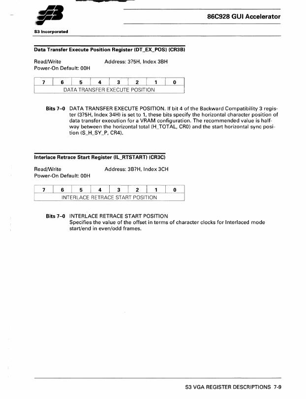
-- -86C928 GUI Accelerator
S3 Incorporated
Data Transfer Execute Position Register (DT _EX_POS) (CR3B)
ReadIWrite Address: 3?5H, Index 3BH Power-On Default: OOH
DATA TRANSFER EXECUTE POSITION
Bits 7-0 DATA TRANSFER EXECUTE POSITION. If bit 4 of the Backward Compatibility 3 register (3?5H, Index 34H) is set to 1, these bits specify the horizontal character position of data transfer execution for a VRAM configuration. The recommended value is halfway between the horizontal total (H_TOTAL, CRO) and the start horizontal sync position (S_H_SY_P, CR4).
Interlace Retrace Start Register (lL_RTSTARTJ (CR3C)
ReadIWrite Address: 3B?H, Index 3CH Power-On Default: OOH
Bits 7-0 INTERLACE RETRACE START POSITION Specifies the value of the offset in terms of character clocks for Interlaced mode start/end in even/odd frames.
S3 VGA REGISTER DESCRIPTIONS 7-9

•.. fa ,. 53 Incorporated
86C928 GUI Accelerator
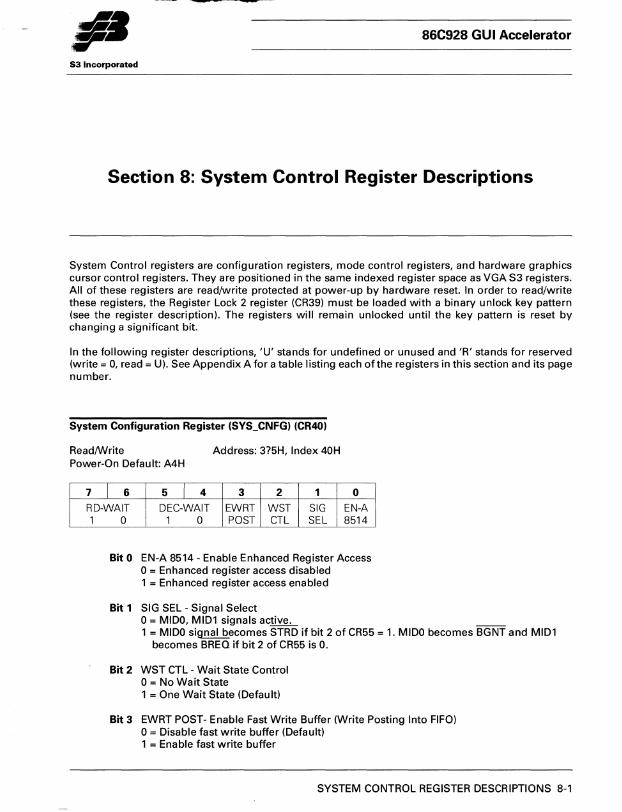
- -,I. 86C928 GUI Accelerator
53 Incorporated
Section 8: System Control Register Descriptions
System Control registers are configuration registers, mode control registers, and hardware graphics cursor control registers. They are positioned in the same indexed register space as VGA S3 registers. All of these registers are read/write protected at power-up by hardware reset. In order to read/write these registers, the Register Lock 2 register (CR39) must be loaded with a binary unlock key pattern (see the register description). The registers will remain unlocked until the key pattern is reset by changing a significant bit.
In the following register descriptions, 'U' stands for undefined or unused and 'R' stands for reserved (write = 0, read = U). See Appendix A for a table listing each ofthe registers in this section and its page number.
System Configuration Register (SYS_CNFG) (CR40)
Read/Write Address: 3?5H, Index 40H Power-On Default: A4H
7 1 6 5 j 4 3 2 1 0
RD-WAIT DEC-WAIT EWRT WST SIG EN-A 1 0 1 0 POST CTL SEL 8514
Bit 0 EN-A 8514 - Enable Enhanced Register Access 0= Enhanced register access disabled 1 = Enhanced register access enabled
Bit 1 SIG SEL - Signal Select 0= MIDO, MID1 signals active. 1 = MIDO signal becomes STRD if bit 2 of CR55 = 1. MIDO becomes BGNT and MID1
becomes BREQ if bit 2 of CR55 is O.
Bit 2 WST CTL - Wait State Control 0= No Wait State 1 = One Wait State (Default)
Bit 3 EWRT POST- Enable Fast Write Buffer (Write Posting Into FIFO) 0= Disable fast write buffer (Default) 1 = Enable fast write buffer
SYSTEM CONTROL REGISTER DESCRIPTIONS 8-1
86C928 GUI Accelerator
53 Incorporated
Bits 5-4 DEC-WAIT - Decode Wait Control (386/486 Local Bus Only) 00 = 0 wait states 01 = 1 wait state 10 = 3 wait states (Default) 11 = 2 wait states
Bits 7-6 RD-WAIT - Read Wait Control 386/486 Local Bus Only 00 = 0 wait states 01 = 1 wait state 10 = 3 wait states (Default) 11 = 2 wait states
ISABusOnl~ 00 = Enable NOWS signal 01 = Disable NOWS signal 10 = Disable NOWS signal (Default) 11 = Disable NOWS signal
BIOS Flag Register (BIOS_FLAG) (CR41)
Read/Write Address: 3?5H, Index 41 H Power-On Default: OOH
7 6 543 2
B IOS-FLAG-REGISTER-l
Bits 7-0 BIOS-FLAG-REGISTER-1
o
Used by the BIOS. Users should not write to this register.
8-2 SYSTEM CONTROL REGISTER DESCRIPTIONS
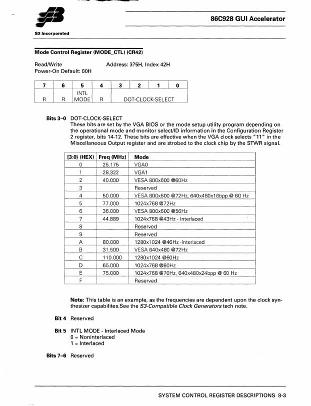
-•• r 86C928 GUI Accelerator
S3 Incorporated
Mode Control Register (MODE_CTL) (CR42)
Read/Write Address: 3?5H, Index 42H Power-On Default: OOH
7
R
6 5 4 3 I 2 I 1 I 0
INTL R MODE R DOT-CLaCK-SELECT
Bits 3-0 DOT-CLaCK-SELECT These bits are set by the VGA BIOS or the mode setup utility program depending on the operational mode and monitor select/I0 information in the Configuration Register 2 register, bits 14-12. These bits are effective when the VGA clock selects" 11" in the Miscellaneous Output register and are strobed to the clock chip by the STWR signal.
[3:0} (HEX) Freq (MHz) Mode
0 25.175 VGAO
1 28.322 VGA1
2 40.000 VESA 800x600 @60Hz
3 Reserved
4 50.000 VESA 800x600 @72Hz, 640x480x16bpp @ 60 Hz
5 77000 1 024x768 @72Hz
6 36.000 VESA 800x600 @56Hz
7 44.889 1024x768@43Hz- Interlaced
8 Reserved
9 Reserved
A 80.000 1280xl024 @46Hz -Interlaced
B 31.500 VESA 640x480 @72Hz
C 110.000 1280x1024 @60Hz
D 65.000 1 024x768 @60Hz
E 75.000 1 024x768 @70Hz, 640x480x24bpp @ 60 Hz
F Reserved
Note: This table is an example, as the frequencies are dependent upon the clock synthesizer capabilites.See the 53-Compatible Clock Generators tech note.
Bit 4 Reserved
Bit 5 INTL MODE - Interlaced Mode 0= Noninteriaced 1 = Interlaced
Bits 7-6 Reserved
SYSTEM CONTROL REGISTER DESCRIPTIONS 8-3
53 Incorporated
Extended Mode Register (EXT_MODE) (CR43)
ReadIWrite Address: 3?5H, Index 43H Power-On Default: OOH
7 6 5 4 3 2 1 0
HCTR 64K OLD OLD DCK X2 R R XEN CLR LSW8 RS2 EDG
Bit 0 DCK EDG - Video Clock Edge Mode Select 0= Normal (Rising Edge Only) 1 = Both Edges (Rising and Falling)
Bit 1 OLD RS2 - DAC Register Select Bit2
86C928 GUI Accelerator
Th is is an extension bit of RS[l :0] for video DAC addressing. Th is is disabled if bits 3-2 of the Extended Video DAC Control register (CR55) are not 0,0.
Bit 2 OLD LSW8 - Logical Screen Width Bit 8 This is an extension of the Offset (Screen Width) register (CR13). This is disabled if bits 5-4 of the Extended System Control 2 (CR51) are not 0,0.
Bit 3 64K CLR - 16-bit Color Mode 0= Disable 16-bit color mode 1 = Enable 16-bit color mode
Bit 4 XEN - Translate Enable 0= Use I/O port address X2E8H 1 = Enable I/O port at address X2E8H XOR 3AOH (X148H)
Bits 6-5 Reserved
Bit 7 HCTR X2 - Horizontal Counter Double Mode 0= Disable horizontal counter double mode 1 = Enable horizontal counter double mode (horizontal CRT parameters are doubled)
8-4 SYSTEM CONTROL REGISTER DESCRIPTIONS
-86C928 GUI Accelerator
S3 Incorporated
Hardware Graphics Cursor Mode Register (HGC_MODE) (CR45)
Read/Write Address: 3?5H, Index 45H Power-On Default: OOH
7
R
6 5 4 3 I 2 1 0
ENB HWGC HWC-HSTR HWGC R 485 1280 X3W X2W R ENB
Bit 0 HWGC ENB - Hardware Graphics Cursor Enable 0= Hardware graphics cursor disabled in any mode 1 = Hardware graphics cursor enabled in Enhanced mode
Bit 1 Reserved
Bit 2 HWC-HSTR X2W - Hardware Cursor Horizontal Stretch 2 0= Function disabled 1 = Stretch to twice width and use the Hardware Graphics Cursor Foreground and
Background Stack registers (CR4A, CR4B), stack pointer 0-1.
Bit 3 HWC-HSTR X3W - Hardware Cursor Horizontal Stretch 3 0= Function disabled 1 = Stretch to triple width and use the Hardware Graphics Cursor Foreground and
Background Stack registers (CR4A, CR4B), stack pointer 0-2
Bit 4 HWGC 1280 - Hardware Cursor Right Storage 0= Function disabled 1 = If 4 bits/pixel, 4 blocks of last 256 bytes in each 1 KByte line of HCS-STADR (size
aligned; two LSBs must be 1,1) become the hardware graphics cursor storage area. If 8 bits/pixel, 2 blocks of last 512 bytes in each 2-KByte line of Hardware Graphics Cursor Start Address register (size aligned; two LSBs must be 1,1) become the hardware graphics cursor storage area.
Bit 5 ENB 485 - Cursor Control Enable for Brooktree Bt485 DAC 0= HC[1:0] are unchanged 1 = HC1 becomes the ODF signal and HCO becomes the CDE signal.
Note: This bit is effective only if bit 5 of the Extended Video DAC Control register (3?5H, Index 55) is set to 1.
Bits 7-6 Reserved
SYSTEM CONTROL REGISTER DESCRIPTIONS 8-5
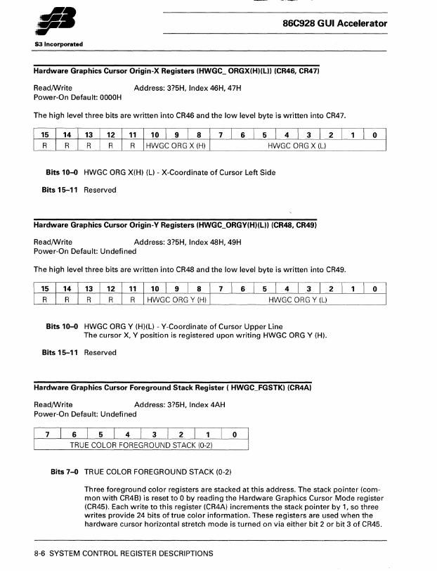
.... r 53 Incorporated
86C928 GUI Accelerator
Hardware Graphics Cursor Origin-X Registers (HWGC_ ORGX(HIIL)) (CR46, CR471
Read/Write Address: 3?5H, Index 46H, 47H Power-On Default: OOOOH
The high level three bits are written into CR46 and the low level byte is written into CR47.
Bits 10-0 HWGC ORG X(HI (LI - X-Coordinate of Cursor Left Side
Bits 15-11 Reserved
Hardware Graphics Cursor Origin-V Registers (HWGC_ORGV(HIIL)) (CR48, CR491
Read/Write Address: 3?5H, Index 48H, 49H Power-On Default: Undefined
The high level three bits are written into CR48 and the low level byte is written into CR49.
Bits 10-0 HWGC ORG V (H)(U - V-Coordinate of Cursor Upper Line The cursor X, Y position is registered upon writing HWGC ORG Y (H).
Bits 15-11 Reserved
Hardware Graphics Cursor Foreground Stack Register ( HWGC_FGSTKI (CR4AI
Read/Write Address: 3?5H, Index 4AH Power-On Default: Undefined
TRUE COLOR FOREGROUND STACK (0-2)
Bits 7-0 TRUE COLOR FOREGROUND STACK (0-2)
Three foreground color registers are stacked at this address. The stack pointer (common with CR4B) is reset to 0 by reading the Hardware Graphics Cursor Mode register (CR45). Each write to this register (CR4A) increments the stack pointer by 1, so three writes provide 24 bits of true color information. These registers are used when the hardware cursor horizontal stretch mode is turned on via either bit 2 or bit 3 of CR45.
8-6 SYSTEM CONTROL REGISTER DESCRIPTIONS
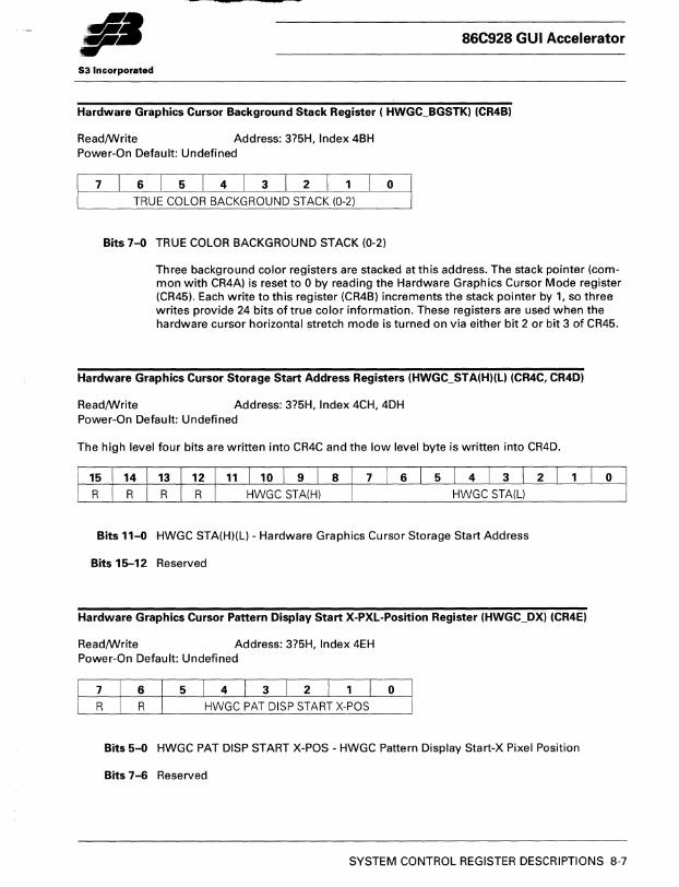
'"' •• r 86C928 GUI Accelerator
S3 Incorporated
Hardware Graphics Cursor Background Stack Register ( HWGC_BGSTK) (CR4B)
Read/Write Address: 3?5H, Index 4BH Power-On Default: Undefined
Bits 7-0 TRUE COLOR BACKGROUND STACK (0-2)
Three background color registers are stacked at this address. The stack pointer (common with CR4A) is reset to 0 by reading the Hardware Graphics Cursor Mode register (CR45). Each write to this register (CR4B) increments the stack pointer by 1, so three writes provide 24 bits of true color information. These registers are used when the hardware cursor horizontal stretch mode is turned on via either bit 2 or bit 3 of CR45.
Hardware Graphics Cursor Storage Start Address Registers (HWGC_STA(H)(L) (CR4C, CR4D)
Read/Write Address: 3?5H, Index 4CH, 4DH Power-On Default: Undefined
The high level four bits are written into CR4C and the low level byte is written into CR4D.
Bits 11-0 HWGC STA(H)(L) - Hardware Graphics Cursor Storage Start Address
Bits 15-12 Reserved
Hardware Graphics Cursor Pattern Display Start X-PXL-Position Register (HWGC_DX) (CR4E)
Read/Write Address: 3?5H, Index 4EH Power-On Default: Undefined
7 6 54321 0
R R HWGC PAT DISP START X-POS
Bits 5-0 HWGC PAT DISP START X-POS - HWGC Pattern Display Start-X Pixel Position
Bits 7-6 Reserved
SYSTEM CONTROL REGISTER DESCRIPTIONS 8-7
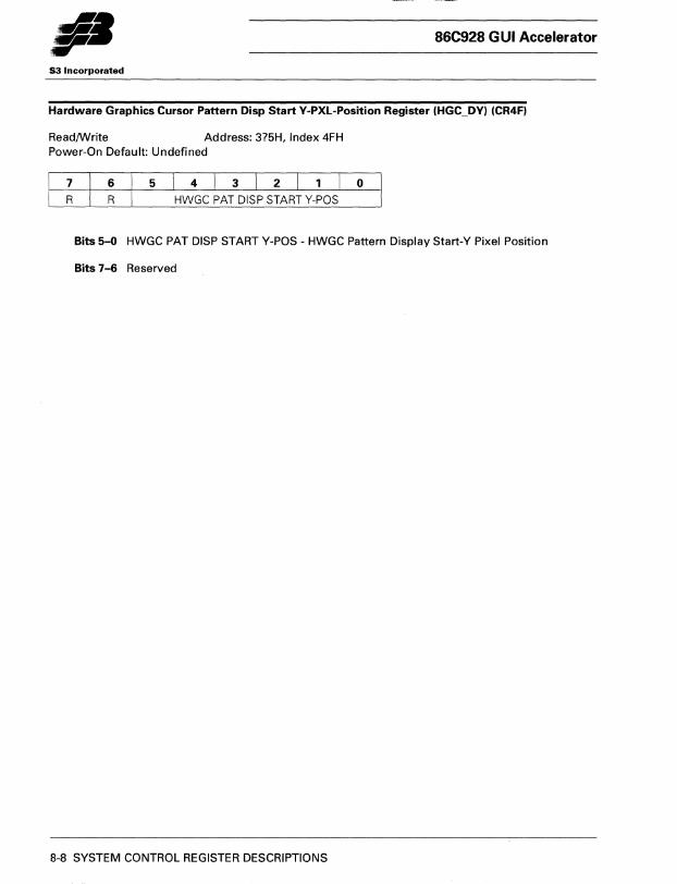
fl· 86C928 GUI Accelerator
53 Incorporated
Hardware Graphics Cursor Pattern Disp Start V-PXL-Position Register (HGC_DV) (CR4F)
Read/Write Address: 3?5H, Index 4FH Power-On Default: Undefined
7 6 54321 0
R R HWGC PAT DISP START Y-POS
Bits 5-0 HWGC PAT DISP START Y-POS - HWGC Pattern Display Start-Y Pixel Position
Bits 7-6 Reserved
8-8 SYSTEM CONTROL REGISTER DESCRIPTIONS
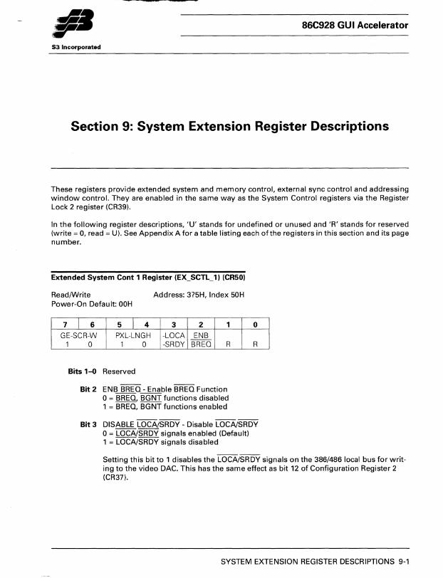
II· 86C928 GUI Accelerator
S3 Incorporated
Section 9: System Extension Register Descriptions
These registers provide extended system and memory control, external sync control and addressing window control. They are enabled in the same way as the System Control registers via the Register Lock 2 register (CR39).
In the following register descriptions, 'U' stands for undefined or unused and 'R' stands for reserved (write = 0, read = U). See Appendix A for a table listing each ofthe registers in this section and its page number.
Extended System Cont 1 Register (EX_SCTL_1) (CR50)
ReadIWrite Address: 3?5H, Index 50H Power-On Default: OOH
7 I 6 5 I 4 3 2 1 0
GE-SCR-W PXL-LNGH -LOCA ENB 1 0 1 0 -SRDY BRED R
Bits 1-0 Reserved
Bit 2 ENB BREO - Enable BREO Function o = BREO, BGNT functions disabled 1 = BREO, BGNT functions enabled
R
Bit 3 DISABLE LOCA/SRDY - Disable LOCA/SRDY 0= LOCA/SRDY signals enabled (Default) 1 = LOCA/SRDY signals disabled
Setting this bit to 1 disables the LOCA/SRDY signals on the 386/486 local bus for writing to the video DAC. This has the same effect as bit 12 of Configuration Register 2 (CR37).
SYSTEM EXTENSION REGISTER DESCRIPTIONS 9-1
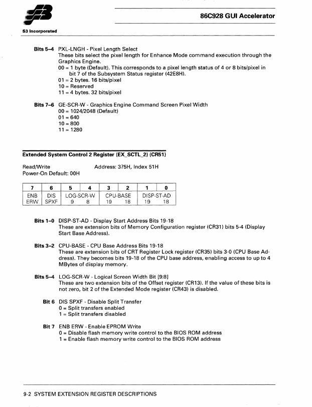
-~. r 86C928 GUI Accelerator
53 Incorporated
Bits 5-4 PXL-LNGH - Pixel Length Select These bits select the pixel length for Enhance Mode command execution through the Graphics Engine. 00 = 1 byte (Defau It). This corresponds to a pixel length status of 4 or 8 bits/pixel in
bit 7 of the Subsystem Status register (42E8H). 01 = 2 bytes. 16 bits/pixel 10 = Reserved 11 = 4 bytes. 32 bits/pixel
Bits 7-6 GE-SCR-W - Graphics Engine Command Screen Pixel Width 00 = 1024/2048 (Default) 01 = 640 10 = 800 11 = 1280
Extended System Control 2 Register (EX_SCTL_2) (CR51)
ReadIWrite Address: 3?5H, Index 51 H Power-On Default: OOH
7 6 5 I 4 3 J 2 1 I 0
ENB DIS LOG-SCR-W CPU-BASE DISP-ST-AD ERW SPXF 9 8 19 18 19 18
Bits 1-0 DISP-ST-AD - Display Start Address Bits 19-18 These are extension bits of Memory Configuration register (CR31) bits 5-4 (Display Start Base Address).
Bits 3-2 CPU-BASE - CPU Base Address Bits 19-18 These are extension bits of CRT Register Lock register (CR35) bits 3-0 (CPU Base Address). They becomes bits 19-18 of the CPU base address, enabling access to up to 4 MBytes of display memory.
Bits 5-4 LOG-SCR-W - Logical Screen Width Bit [9:8] These are two extension bits of the Offset register (CR13). If the value of these bits is not zero, bit 2 of the Extended Mode register (CR43) is disabled.
Bit 6 DIS SPXF - Disable Split Transfer o = Split transfers enabled 1 = Split transfers disabled
Bit 7 ENB ERW - Enable EPROM Write o = Disable flash memory write control to the BIOS ROM address 1 = Enable flash memory write control to the BIOS ROM address
9-2 SYSTEM EXTENSION REGISTER DESCRIPTIONS
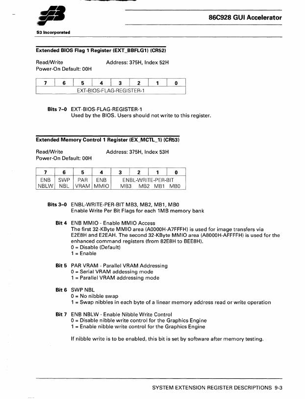
II· 86C928 GUI Accelerator
S3 Incorporated
Extended BIOS Flag 1 Register (EXT_BBFLG1) (CR52)
ReadIWrite Address: 3?5H, Index 52H Power-On Default: OOH
7 6 5 4 3 2 o EXT-BIOS-FLAG-REGISTER-l
Bits 7-0 EXT-BIOS-FLAG-REGISTER-l Used by the BIOS. Users should not write to this register.
Extended Memory Control 1 Register (EX_MCTL_1) (CR53)
ReadIWrite Address: 3?5H, Index 53H Power-On Default: OOH
7 6 5 4 3 I 2 I 1 I 0
ENB SWP PAR ENB ENBL -WR ITE-PER-BIT NBLW NBL VRAM MMIO MB3 MB2 MBl MBO
Bits 3-0 ENBL-WRITE-PER-BIT MB3, MB2, MB1, MBO Enable Write Per Bit Flags for each 1MB memory bank
Bit 4 ENB MMIO - Enable MMIO Access The first 32-KByte MMIO area (AOOOOH-A7FFFH) is used for image transfers via E2E8H and E2EAH. The second 32-KByte MMIO area (A8000H-AFFFFH) is used for the enhanced command registers (from 82E8H to BEE8H). 0= Disable (Default) 1 = Enable
Bit 5 PAR VRAM - Parallel VRAM Addressing o = Serial VRAM addessing mode 1 = Parallel VRAM addressing mode
Bit 6 SWP NBL 0= No nibble swap 1 = Swap nibbles in each byte of a linear memory address read or write operation
Bit 7 ENB NBLW - Enable Nibble Write Control 0= Disable nibble write control for the Graphics Engine 1 = Enable nibble write control for the Graphics Engine
If nibble write is to be enabled, this bit is set by software after memory testing.
SYSTEM EXTENSION REGISTER DESCRIPTIONS 9-3
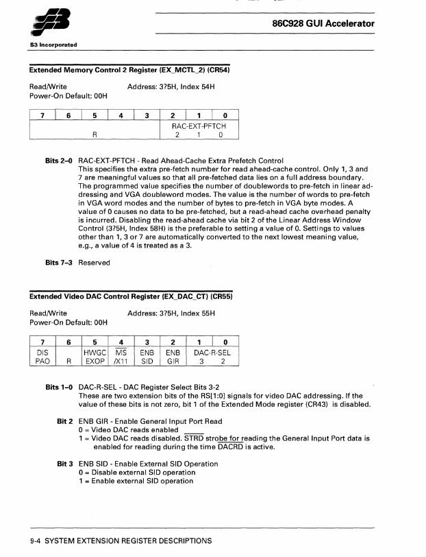
86C928 GUI Accelerator
S3 Incorporated
Extended Memory Control 2 Register (EX_MCTL_2) (CR54)
Read/Write Address: 3?5H, Index 54H Power-On Default: OOH
7 6 5 4 3 210
RAC-EXT-PFTCH R 2 1 a
Bits 2-0 RAC-EXT-PFTCH - Read Ahead-Cache Extra Prefetch Control This specifies the extra pre-fetch numberfor read ahead-cache control. Only 1,3 and 7 are meaningful values so that all pre-fetched data lies on a full address boundary. The programmed value specifies the number of doublewords to pre-fetch in linear addressing and VGA doubleword modes. The value is the number of words to pre-fetch in VGA word modes and the number of bytes to pre-fetch in VGA byte modes. A value of 0 causes no data to be pre-fetched, but a read-ahead cache overhead penalty is incurred. Disabling the read-ahead cache via bit 2 ofthe Linear Address Window Control (3?5H, Index 58H) is the preferable to setting a value of o. Settings to values other than 1,3 or 7 are automatically converted to the next lowest meaning value, e.g., a value of 4 is treated as a 3.
Bits 7-3 Reserved
Extended Video DAC Control Register (EX_DAC_CT) (CR55)
Read/Write Address: 3?5H, Index 55H Power-On Default: OOH
7 6 5 4 3 2 1 I 0
DIS HWGC MS ENB ENB DAC-R-SEL PAO R EXOP /Xll SID GIR 3 2
Bits 1-0 DAC-R-SEL - DAC Register Select Bits 3-2 These are two extension bits of the RS[1 :0] signals for video DAC addressing. If the value of these bits is not zero, bit 1 of the Extended Mode register (CR43) is disabled.
Bit 2 ENB GIR - Enable General Input Port Read 0= Video DAC reads enabled 1 = Video DAC reads disabled. STRD strobe for reading the General Input Port data is
enabled for reading during the time DACRD is active.
Bit 3 ENB SID - Enable External SID Operation 0= Disable external SID operation 1 = Enable external SID operation
9-4 SYSTEM EXTENSION REGISTER DESCRIPTIONS
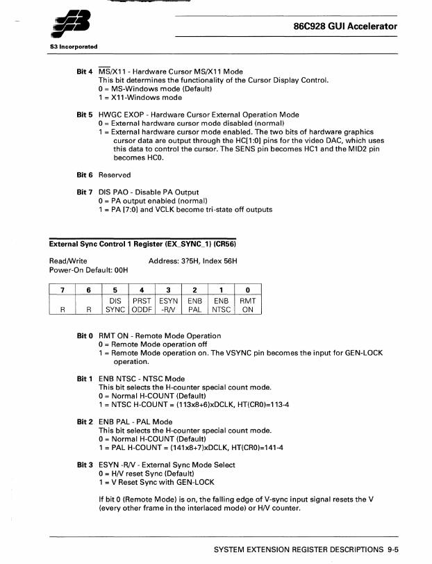
-.... r 86C928 GUI Accelerator
S3 Incorporated
Bit 4 MS/X11 - Hardware Cursor MS/X11 Mode This bit determines the functionality of the Cursor Display Control. o = MS-Windows mode (Default) 1 = X11-Windows mode
Bit 5 HWGC EXOP - Hardware Cursor External Operation Mode 0= External hardware cursor mode disabled (normal) 1 = External hardware cursor mode enabled. The two bits of hardware graphics
cursor data are output through the HC[1 :0] pins for the video DAC, which uses this data to control the cursor. The SENS pin becomes HC1 and the MID2 pin becomes HCO.
Bit 6 Reserved
Bit 7 DIS PAO - Disable PA Output 0= PA output enabled (normal) 1 = PA [7:0] and VCLK become tri-state off outputs
External Sync Control' Register (EX_SYNC_,) (CR56)
ReadIWrite Address: 3?5H, Index 56H Power-On Default: OOH
7
R
6 5 4 3 2 , 0
DIS PRST ESYN ENB ENB RMT R SYNC ODDF -RN PAL NTSC ON
Bit 0 RMT ON - Remote Mode Operation 0= Remote Mode operation off 1 = Remote Mode operation on. The VSYNC pin becomes the input for GEN-LOCK
operation.
Bit' ENB NTSC - NTSC Mode This bit selects the H-counter special count mode. 0= Normal H-COUNT (Default) 1 = NTSC H-COUNT = (113x8+6)xDCLK, HT(CRO)=113-4
Bit 2 ENB PAL - PAL Mode This bit selects the H-counter special count mode. 0= Normal H-COUNT (Default) 1 = PAL H-COUNT = (141x8+7)xDCLK, HT(CRO)=141-4
Bit 3 ESYN -RN - External Sync Mode Select 0= HN reset Sync (Default) 1 = V Reset Sync with GEN-LOCK
If bit 0 (Remote Mode) is on, the falling edge of V-sync input signal resets the V (every other frame in the interlaced mode) or HN counter.
SYSTEM EXTENSION REGISTER DESCRIPTIONS 9-5
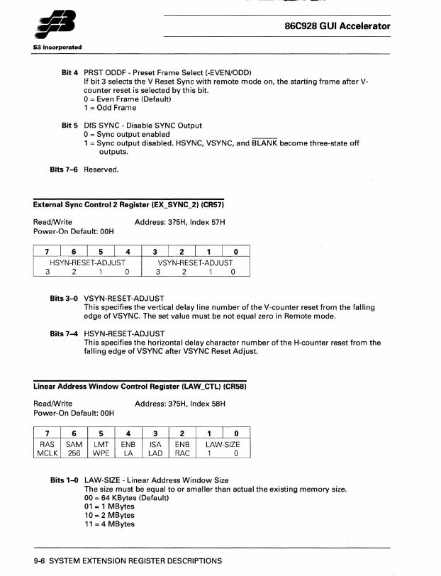
86C928 GUI Accelerator
S3 Incorporated
Bit 4 PRST ODDF - Preset Frame Select (-EVEN/ODD) If bit 3 selects the V Reset Sync with remote mode on, the starting frame after Vcounter reset is selected by th is bit. 0= Even Frame (Default) 1 = Odd Frame
Bit 5 DIS SYNC - Disable SYNC Output o = Sync output enabled 1 = Sync output disabled. HSYNC, VSYNC, and BLANK become three-state off
outputs.
Bits 7-6 Reserved.
External Sync Control 2 Register (EX_SVNC_2) (CR57)
ReadIWrite Address: 3?5H, Index 57H Power-On Default: OOH
7
3
I 6 I 5 I 4 3 I 2 I 1 I 0 HSYN-RESET-ADJUST VSYN-RESET-ADJUST
2 1 0 3 2 1 0
Bits 3-0 VSYN-RESET-ADJUST This specifies the vertical delay line number ofthe V-counter reset from the falling edge ofVSYNC. The set value must be not equal zero in Remote mode.
Bits 7-4 HSYN-RESET-ADJUST This specifies the horizontal delay character number of the H-counter reset from the falling edge of VSYNC after VSYNC Reset Adjust.
Linear Address Window Control Register (LAW_CTL) (CR58)
ReadIWrite Address: 3?5H, Index 58H Power-On Defau It: OOH
7 6 5 4 3 2 1 I 0 RAS SAM LMT ENB ISA ENB LAW-SIZE
MCLK 256 WPE LA LAD RAC 1 0
Bits 1-0 LAW-SIZE - Linear Address Window Size The size must be equal to or smaller than actual the existing memory size. 00 = 64 KBytes (Default) 01 = 1 MBytes 10 = 2 MBytes 11 = 4 MBytes
9-6 SYSTEM EXTENSION REGISTER DESCRIPTIONS
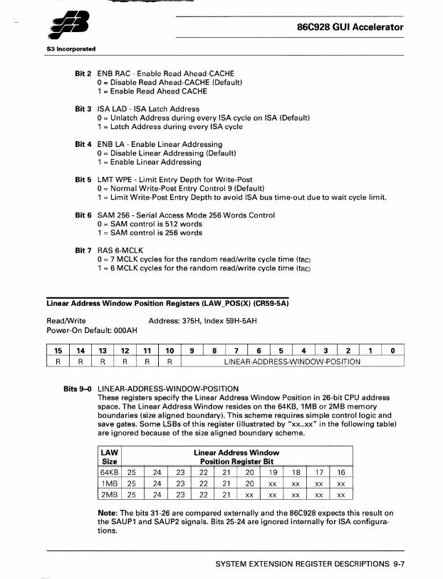
86C928 GUI Accelerator
S3 Incorporated
Bit 2 ENB RAC - Enable Read Ahead-CACHE o = Disable Read Ahead-CACHE (Default) 1 = Enable Read Ahead CACHE
Bit 3 ISA LAD - ISA Latch Address 0= Unlatch Address during every ISA cycle on ISA (Default) 1 = Latch Address during every ISA cycle
Bit 4 ENB LA - Enable Linear Addressing 0= Disable Linear Addressing (Default) 1 = Enable Linear Addressing
Bit 5 LMT WPE - Limit Entry Depth for Write-Post o = Normal Write-Post Entry Control 9 (Default) 1 = Limit Write-Post Entry Depth to avoid ISA bus time-out due to wait cycle limit.
Bit 6 SAM 256 - Serial Access Mode 256 Words Control 0= SAM control is 512 words 1 = SAM control is 256 words
Bit 7 RAS 6-MCLK 0=7 MCLK cycles for the random read/write cycle time (tRC) 1 = 6 MCLK cycles for the random read/write cycle time (tRC)
Linear Address Window Position Registers (LAW_POS(X) (CR59-5A)
Read/Write Address: 3?5H, Index 59H-5AH Power-On Default: OOOAH
Bits 9-0 LlNEAR-ADDRESS-WINDOW-POSITION These registers specify the Linear Address Window Position in 26-bit CPU address space. The Linear Address Window resides on the 64KB, 1MB or 2MB memory boundaries (size aligned boundary). This scheme requires simple control logic and save gates. Some LSBs ofthis register (illustrated by "xx .. xx" inthe following table) are ignored because of the size aligned boundary scheme.
LAW Linear Address Window Size Position Reaister Bit 64KB 25 24 23 22 21 20 19 18 17 16
1MB 25 24 23 22 21 20 xx xx xx xx
2MB 25 24 23 22 21 xx xx xx xx xx
Note: The bits 31-26 are compared externally and the 86C928 expects this result on the SAUP1 and SAUP2 signals. Bits 25-24 are ignored internally for ISA configurations.
SYSTEM EXTENSION REGISTER DESCRIPTIONS 9-7
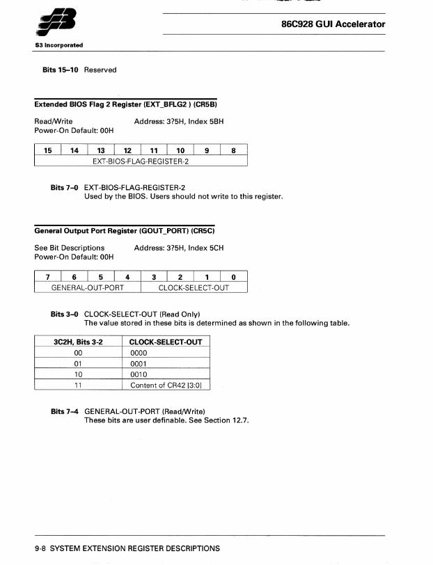
•• r 86C928 G UI Accelerator
53 Incorporated
Bits 15-10 Reserved
Extended BIOS Flag 2 Register (EXT _BFlG2 ) (CR5B)
Read/Write Address: 3?5H, Index 5BH Power-On Default: OOH
I 15 I 14 I 13 I 12 I 11 I 10 I 9 8
EXT-BIOS-FLAG-REGISTER-2
Bits 7...{J EXT-BIOS-FLAG-REGISTER-2 Used by the BIOS. Users should not write to this register.
General Output Port Register (GOUT_PORT) (CR5C)
See Bit Descriptions Power-On Default: OOH
Address: 3?5H, Index 5CH
Bits 3...{J CLOCK-SELECT-OUT (Read Only) The value stored in these bits is determined as shown in the following table.
3C2H, Bits 3-2 CLOCK-SELECT-OUT
00 0000
01 0001
10 0010
11 Content of CR42 [3:0]
Bits 7-4 GENERAL-OUT-PORT (Read/Write) These bits are user definable. See Section 12.7.
9-8 SYSTEM EXTENSION REGISTER DESCRIPTIONS
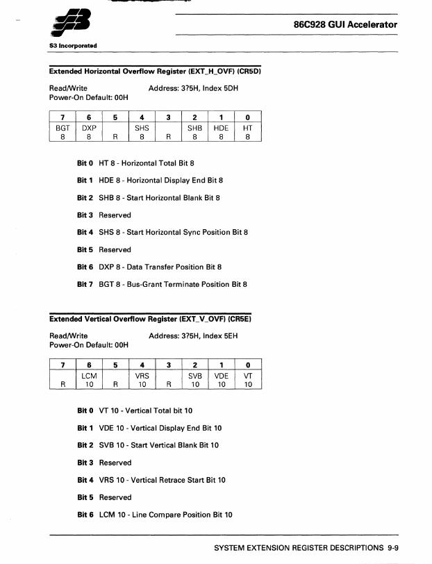
fl· 86C928 GUI Accelerator
S3 Incorporated
Extended Horizontal Overflow Register (EXT_H_OVFI (CR5DI
Read/Write Address: 3?5H, Index 5DH Power-On Default: OOH
7 6 5 4 3 2 1 0
BGT DXP SHS SHB HDE HT 8 8 R 8 R 8 8 8
Bit 0 HT 8 - Horizontal Total Bit 8
Bit 1 HDE 8 - Horizontal Display End Bit 8
Bit 2 SHB 8 - Start Horizontal Blank Bit 8
Bit 3 Reserved
Bit 4 SHS 8 - Start Horizontal Sync Position Bit 8
Bit 5 Reserved
Bit 6 DXP 8 - Data Transfer Position Bit 8
Bit 7 BGT 8 - Bus-Grant Terminate Position Bit 8
Extended Vertical Overflow Register (EXT_V_OVFI (CR5EI
Read/Write Address: 3?5H, Index 5EH Power-On Default: OOH
7 6 5 4 3 2 1 0 LCM VRS SVB VDE VT
R 10 R 10 R 10 10 10
Bit 0 VT 10 - Vertical Total bit 10
Bit 1 VDE 10 - Vertical Display End Bit 10
Bit 2 SVB 10 - Start Vertical Blank Bit 10
Bit 3 Reserved
Bit 4 VRS 10 - Vertical Retrace Start Bit 10
Bit 5 Reserved
Bit 6 LCM 10 - Line Compare Position Bit 10
SYSTEM EXTENSION REGISTER DESCRIPTIONS 9-9
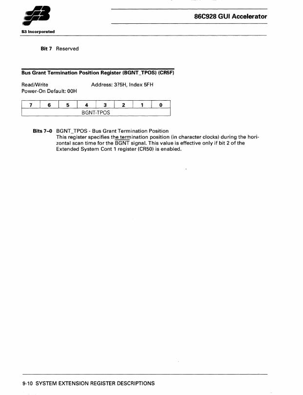
86C928 GUI Accelerator
S3 Incorporated
Bit 7 Reserved
Bus Grant Termination Position Register (BGNT_TPOS) (CR5F)
ReadIWrite Address: 3?5H, Index 5FH Power-On Default: OOH
7 6 5 4 3 2 o BGNT-TPOS
Bits 7-0 BGNT _TPOS - Bus Grant Termination Position This register specifies the termination position (in character clocks) during the horizontal scan time for the BGNT signal. This value is effective only if bit 2 of the Extended System Cont 1 register (CR50) is enabled.
9-10 SYSTEM EXTENSION REGISTER DESCRIPTIONS
-.l~ rill 53 Incorporated
86C928 GUI Accelerator
Section 10: Enhanced Commands Register Descriptions
These registers support the 86C928 Enhanced drawing commands. Access to these registers is enabled via bit 0 of the System Configuration (3?5H, Index 40) register.
In the following register descriptions, 'U' stands for undefined or unused and 'R' stands for reserved (write = 0, read = U). See Appendix A for a table listing each ofthe registers in this section and its page number.
Subsystem Status Register (SUBSVS_STAT)
Read Only Address: 42E8H Power-On Default: OOOOH
This read-only register provides information on interrupt status, monitor I.D. and the number of bits per pixel. See the Subsystem Control (42E8H, Write Only) register for details on enabling and clearing interrupts.
15
R
14 13 12 11 10 9 8
R R R R R R R
Bit 0 VSV INT - Vertical Sync Interrupt o = No interrupt 1 = Interrupt generated if enabled
7
PXL LNG
Bit 1 GE BSV - Graphics Engine Busy Interrupt o = No interrupt 1 = Interrupt generated if enabled
Bit 2 FIFO OVF - FIFO Overflow Interrupt o = No interrupt 1 = Interrupt generated if enabled
Bit 3 FIFO EMP - FIFO Empty Interrupt 0= No interrupt 1 = Interrupt generated if enabled
6 I 5 I 4 3 2 1 0
MONTR-ID FIFO FIFO GE VSY 2 1 0 EMP OVF BSY INT
ENHANCED COMMANDS REGISTER DESCRIPTIONS 10-1
II· S3 Incorporatad
Bits 6-4 MONTR-ID - Monitor I.D. 010 = 8514/A color 16" 101 = VGA 8503 mono 12" 110 = VGA 8513 color 12"/8512 color 14" 111 = No monitor or other monitor
Bit 7 PXL LNG - Pixel Length (# of bit planes) 0= 4-bit 1 = 8-bit
86C928 GUI Accelerator
The number of bit planes status when bits 5-4 and 7-6 of the Extended System Controll register (CR50) are both 00 is derived from display memory size, memory configuration and screen resolution according to the following table. The actual number of bitplanes is the last number in the screen map column.
System Memory Advanced Subsystem Screen Map Configuration bits Configuration bit 1 Function Control Status bit 7
7-5 bit 2
Memory: Pages: Screen Status: 110 = 1 MByte 0= one Resolution: 0=4 bpp 111 = 0.5 MByte 1 = two 0= 640x480 1 = 8 bpp
1 = 1024x768 or800x600
111 x 0 1 1024x512x8 111 x 1 0 1 024x1 024x4
110 0 x 1 1 024x1 024x8
110 1 0 1 2x1024x512x8 or1024x512x16
110 1 1 0 2048x1024x4
Bits 15-8 Reserved
Subsystem Control Register (SUBSYS_CNTL)
Write Only Address: 42E8H Power-On Default: OOOOH
This register allows each of several interrupt sources to be enabled or disabled. Interrupt status (Subsystem Status (42E8H, Read Only) can be cleared. This register also controls the software reset ofthe graphics engine.
15 I 14 13 12 11 I 10 9 8 7 6 5 4 3 2 1 0
GE-RST FIFO-ENB GE VSY FIFO FIFO GEB VSY 1 0 R R EMP OVF BSY ENB U U U U CLE CLO CLR CLR
10-2 ENHANCED COMMANDS REGISTER DESCRIPTIONS
S3 Incorporated
Bit 0 VSY CLR - Clear Vertical Sync Interrupt Status 0= no change 1 = clear
Bit 1 GEB CLR - Clear Graphics Engine Busy Interrupt Status 0= no change 1 = clear
Bit 2 FIFO CLO - Clear FIFO Overflow Interrupt Status 0= no change 1 = clear
Bit 3 FIFO CLE - Clear FIFO Empty Interrupt Status 0= no change 1 = clear
Bits 7-4 Undefined
Bit 8 VSY ENB - Vertical Sync Interrupt Enable 0= Disable 1 = Enable
Bit 9 GE BSY- Graphics Engine Busy Interrupt Enable 0= Disable 1 = Enable
Bit 10 FIFO-ENB OVF - FIFO Overflow Interrupt Enable 0= Disable 1 = Enable
Bit 11 FIFO-ENB EMP - FIFO Empty Interrupt Enable 0= Disable 1 = Enable
Bits 13-12 Reserved
Bits 15-14 GE-RST - Graphics Engine Software Reset 00 = no change 01 = Graphics Engine enabled 10 = reset 11 = reserved
86C928 GUI Accelerator
ENHANCED COMMANDS REGISTER DESCRIPTIONS 10-3
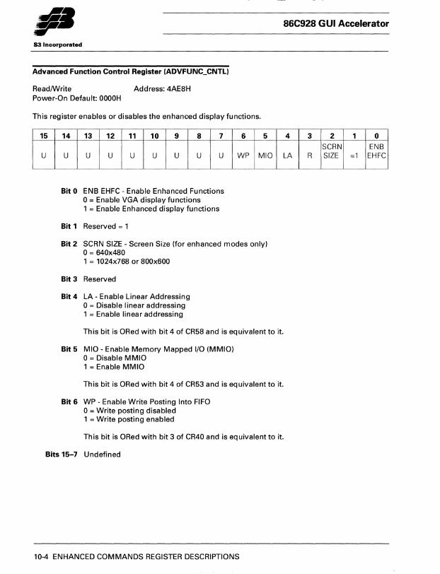
•• r S3 Incorporated
Advanced Function Control Register (ADVFUNC_CNTl)
Read/Write Address: 4AE8H Power-On Default: OOOOH
This register enables or disables the enhanced display functions.
15
U
14 13 12 11 10 9 8 7
U U U U U U U U
Bit 0 ENS EHFC - Enable Enhanced Functions 0= Enable VGA display functions 1 = Enable Enhanced display functions
Bit 1 Reserved = 1
6 5
WP MIO
Bit 2 SCRN SIZE - Screen Size (for enhanced modes only) 0= 640x480 1 = 1024x768 or 800x600
Bit 3 Reserved
Bit 4 LA - Enable Linear Addressing 0= Disable linear addressing 1 = Enable linear addressing
This bit is ORed with bit 4 of CR58 and is equivalent to it.
Bit 5 MIO - Enable Memory Mapped I/O (MMIO) 0= Disable MMIO 1 = Enable MMIO
This bit is ORed with bit 4 of CR53 and is equivalent to it.
Bit 6 WP - Enable Write Posting Into FIFO o = Write posting disabled 1 = Write posting enabled
86C928 GUI Accelerator
4 3 2 1 0
SCRN ENB LA R SIZE =1 EHFC
This bit is ORed with bit 3 of CR40 and is equivalent to it.
Bits 15-7 Undefined
10-4 ENHANCED COMMANDS REGISTER DESCRIPTIONS
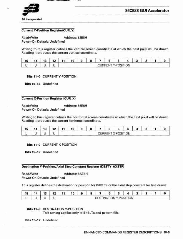
86C928 GUI Accelerator
S3 Incorporated
Current V-Position Register(CUR_ VI
ReadIWrite Address: 82E8H Power-On Default: Undefined
Writing to this register defines the vertical screen coordinate at which the next pixel will be drawn. Reading it produces the current vertical coordinate.
Bits 11-0 CURRENT V-POSITION
Bits 15-12 Undefined
Current X-Position Register (CUR_Xl
ReadIWrite Address: 86E8H Power-On Default: Undefined
Writing to this register defines the horizontal screen coordinate at which the next pixel will be drawn. Reading it produces the current horizontal coordinate.
Bits 11-0 CURRENT X-POSITION
Bits 15-12 Undefined
Destination V-Position/Axial Step Constant Register (DESTV_AXSTPI
ReadIWrite Address: 8AE8H Power-On Default: Undefined
Th is register defines the destination V position for BitBL Ts or the axial step constant for line draws.
Bits 11-0 DESTINATION V-POSITION This setting applies only to BitBLTs and pattern fills.
Bits 15-12 Undefined
ENHANCED COMMANDS REGISTER DESCRIPTIONS 10-5
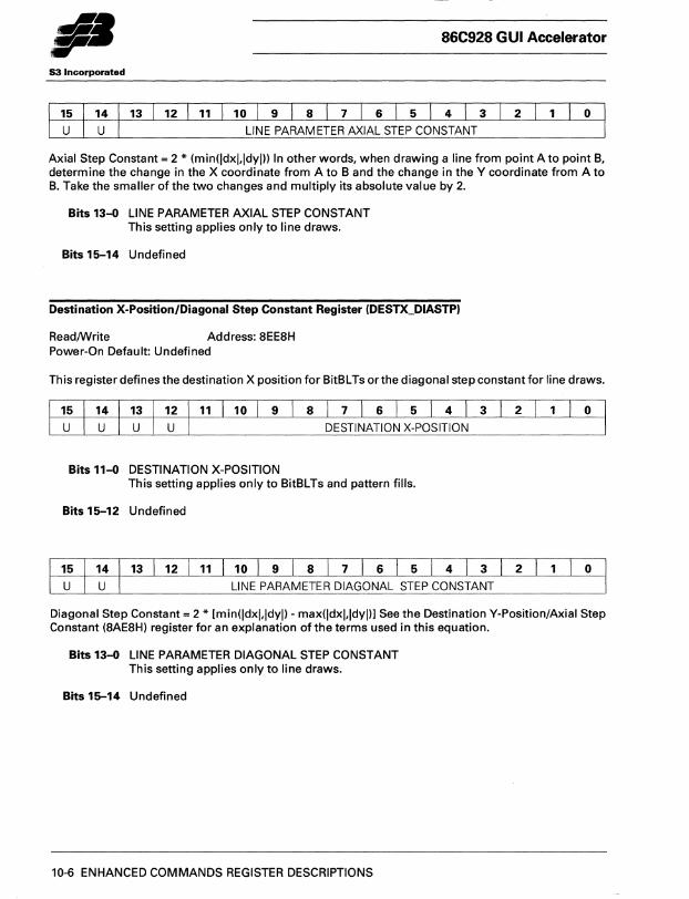
•• r 86C928 GUI Accelerator
S3 Incorporated
Axial Step Constant = 2 * (minqdxl,ldyll) In other words, when drawing a line from point A to point B, determine the change in the X coordinate from A to B and the change in the V coordinate from A to B. Take the smaller of the two changes and multiply its absolute value by 2.
Bits 13-0 LINE PARAMETER AXIAL STEP CONSTANT This setting applies only to line draws.
Bits 15-14 Undefined
Destination X-Position/Diagonal Step Constant Register (DESTX_DIASTP)
ReadIWrite Address: 8EE8H Power-On Default: Undefined
This register defines the destination X position for BitBL Ts orthe diagonal step constant for line draws.
Bits 11-0 DESTINATION X-POSITION This setting applies only to BitBLTs and pattern fills.
Bits 15-12 Undefined
LINE PARAMETER DIAGONAL STEP CONSTANT
Diagonal Step Constant = 2 * [minqdxl,ldyll- maxqdxl,ldYlll See the Destination V-Position/Axial Step Constant (8AE8H) register for an explanation of the terms used in this equation.
Bits 13-0 LINE PARAMETER DIAGONAL STEP CONSTANT This setting applies only to line draws.
Bits 15-14 Undefined
10-6 ENHANCED COMMANDS REGISTER DESCRIPTIONS
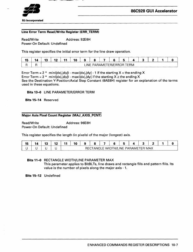
II· 86C928 GUI Accelerator
S3 Incorporated
Line Error Term Read/Write Register (ERR_TERM)
ReadIWrite Address: 92E8H Power-On Default: Undefined
This register specifies the initial error term for the line draw operation.
LINE PARAMETER/ERROR TERM
Error Term = 2 * min(ldxl,ldyll- max(ldxl,ldyl- 1 if the starting X < the ending X Error Term = 2 * min(ldxl,ldyll- max(ldxl,ldyl ifthe starting X;:: the ending X See the Destination V-Position/Axial Step Constant (8AE8H) register for an explanation of the terms used in these equations.
Bits 13-0 LINE PARAMETER/ERROR TERM
Bits 15-14 Reserved
Major Axis Pixel Count Register (MAJ_AXIS_PCNT)
ReadIWrite Address: 96E8H Power-On Default: Undefined
This register specifies the length (in pixels) of the major (longest) axis.
Bits 11-0 RECTANGLE WIDTH/LINE PARAMETER MAX This parameter applies to BitBL Ts, line draws and rectangle fills and pattern fills. Its value is the number of pixels along the major axis - 1.
Bits 15-12 Undefined
ENHANCED COMMANDS REGISTER DESCRIPTIONS 10-7
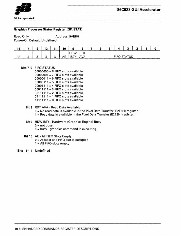
•• r 86C928 GUI Accelerator
S3 Incorporated
Graphics Processor Status Register (GP _STAT)
Read Only Address: 9AE8H Power-On Default: Undefined
15 14 13 12 11 10 9 8 7 I 6 I 5 I 4 I 3 121 1 I 0
U HDW RDT
U U U U AE BSY AVA
Bits 7-0 FIFO-STATUS 00000000 = 8 FIFO slots available 00000001 = 7 FIFO slots available 00000011 = 6 FIFO slots available 00000111 = 5 FIFO slots available 00001111 = 4 FIFO slots available 00011111 = 3 FIFO slots available 00111111 = 2 FIFO slots available 01111111 = 1 FIFO slots available 11111111 = 0 FIFO slots available
Bit 8 RDT AVA - Read Data Available
FIFO-STATUS
0= No read data is available in the Pixel Data Transfer (E2E8H) register. 1 = Read data is available in the Pixel Data Transfer (E2E8H) register.
Bit 9 HDW BSY - Hardware (Graphics Engine) Busy 0= not busy 1 = busy - graphics command is executing
Bit 10 AE - All FIFO Slots Empty o = At least one FIFO slot is occupied 1 = All FIFO slots empty
Bits 15-11 Undefined
10-8 ENHANCED COMMANDS REGISTER DESCRIPTIONS
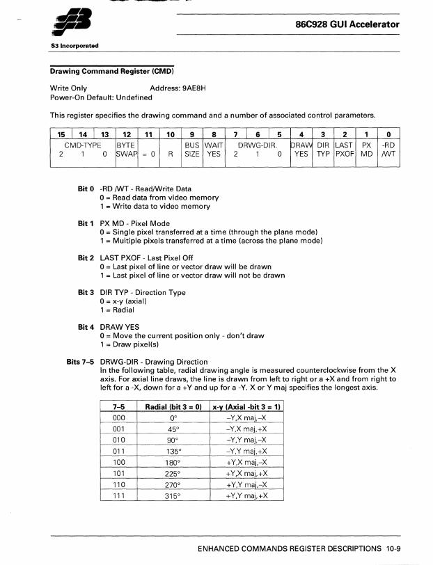
-~--~-
II· 86C928 GUI Accelerator
53 Incorporated
Drawing Command Register (CMD)
Write Only Address: 9AE8H Power-On Default: Undefined
This register specifies the drawing command and a number of associated control parameters.
15 I 14 I 13 12 11 10 9 8 7 I 6 I 5 4 3
2 CMD-TYPE BYTE BUS WAIT
1 0 SWAP = 0 R SIZE YES
Bit 0 -RD /V'JT - Read/Write Data 0= Read data from video memory 1 = Write data to video memory
Bit 1 PX MD - Pixel Mode
DRWG-DIR. PRAVv DIR 2 1 0 YES TYP
0= Single pixel transferred at a time (through the plane mode) 1 = Multiple pixels transferred at a time (across the plane mode)
Bit 2 LAST PXOF - Last Pixel Off 0= Last pixel of line or vector draw will be drawn 1 = Last pixel of line or vector draw will not be drawn
Bit 3 DIR TYP - Direction Type o = x-y (axial) 1 = Radial
Bit 4 DRAW YES 0= Move the current position only - don't draw 1 = Draw pixel(s)
Bits 7-5 DRWG-DIR - Drawing Direction
2 1
LAST PX PXOF MD
0
-RD /VVT
In the following table, radial drawing angle is measured counterclockwise from the X axis. For axial line draws, the line is drawn from left to right or a +X and from right to left for a -X, down for a +Y and up for a -Yo X or Y maj specifies the longest axis.
7-5 Radial (bit 3 = 0) x-v (Axial -bit 3 = 1)
000 0° -Y,X maj,-X
001 45° -Y,X maj,+X
010 90° -Y,Y maj,-X
011 135° -Y,Y maj,+X
100 180° +Y,X maj,-X
101 225° +Y,X maj,+X
110 270° +Y,Y maj,-X
111 315° +Y,Y maj,+X
ENHANCED COMMANDS REGISTER DESCRIPTIONS 10-9
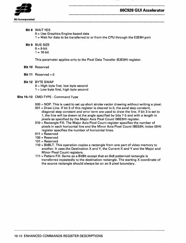
•• r 86C928 GUI Accelerator
53 Incorporated
Bit 8 WAIT YES 0= Use Graphics Engine-based data 1 = Wait for data to be transferred to or from the CPU through the E2E8H port
Bit 9 BUS SIZE 0= 8-bit 1 = 16-bit
This parameter applies only to the Pixel Data Transfer (E2E8H) register.
Bit 10 Reserved
Bit 11 Reserved = 0
Bit 12 BYTE SWAP o = High byte first, low byte second 1 = Low byte first, high byte second
Bits 15-13 CMD-TYPE - Command Type
000 = NOP. This is used to set up short stroke vector drawing without writing a pixel. 001 = Draw Line. If bit 3 of this register is cleared to 0, the axial step constant,
diagonal step constant and error term are used to draw the line. If bit 3 is set to 1, the line will be drawn at the angle specified by bits 7-5 and with a length in pixels as specified by the Major Axis Pixel Count (96E8H) register.
010 = Rectangle Fill. The Major Axis Pixel Count register specifies the number of pixels in each horizontal line and the Minor Axis Pixel Count (BEE8H, Index OOH) register specifies the number of horizontal lines.
011 = Reserved 100 = Reserved 101 = Reserved 110 = BitBL T. This operation copies a rectangle from one part of video memory to
another. It uses the Destination X and Y, the Current X and Y and the Major and Minor Pixel Count registers.
111 = Pattern Fill. Same as a BitBlt except that an 8x8 patterned rectangle is transferred repeatedly to the destination rectangle. The starting X coordinate of the source rectangle should always be on an 8 pixel boundary.
10-10 ENHANCED COMMANDS REGISTER DESCRIPTIONS
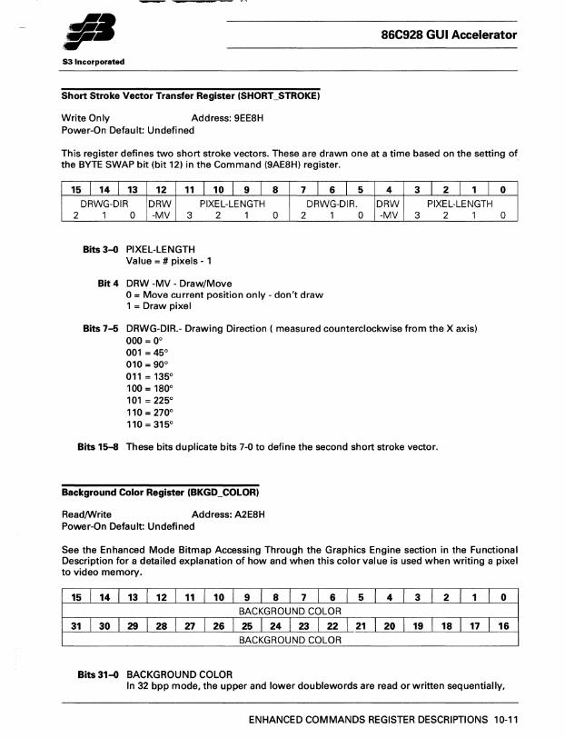
86C928 GUI Accelerator
53 Incorporated
Short Stroke Vector Transfer Register (SHORT_STROKE)
Write Only Address: 9EE8H Power-On Default: Undefined
This register defines two short stroke vectors. These are drawn one at a time based on the setting of the BYTE SWAP bit (bit 12) in the Command (9AE8H) register.
15 I 14 I 13 12 11 I 10 I 9 I 8 7 I 6 I 5
2 DRWG-DIR DRW PIXEL-LENGTH DRWG-DIR.
1 0 -MV 3
Bits 3-0 PIXEL-LENGTH Value = # pixels - 1
2
Bit 4 DRW -MV - Draw/Move
1 0 2
0= Move current position only - don't draw 1 = Draw pixel
1 0
4 3 I 2 I 1 I DRW PIXEL-LENGTH -MV 3 2 1
Bits 7-5 DRWG-DIR.- Drawing Direction ( measured counterclockwise from the X axis) 000 = 00
001 = 450
010 = 900
011 = 1350
100 = 1800
101 = 2250
110 = 2700
110 = 3150
Bits 15-8 These bits duplicate bits 7-0 to define the second short stroke vector.
Background Color Register (BKGD_COLOR)
ReadIWrite Address: A2E8H Power-On Default: Undefined
0
0
See the Enhanced Mode Bitmap Accessing Through the Graphics Engine section in the Functional Description for a detailed explanation of how and when this color value is used when writing a pixel to video memory.
15 I 14 I 13 I 12 I 11 I 10 I 9 I 8 I 7 I 6 I 5 1 4 I 3 121 1 I 0
BACKGROUND COLOR
31 I 30 I 29 I 28 I 27 I 26 I 25 I 24 I 23 I 22 I 21 I 20 I 19 I 18 I 17 I 16
BACKGROUND COLOR
Bits 31-0 BACKGROUND COLOR In 32 bpp mode, the upper and lower doublewords are read or written sequentially,
ENHANCED COMMANDS REGISTER DESCRIPTIONS 10-11
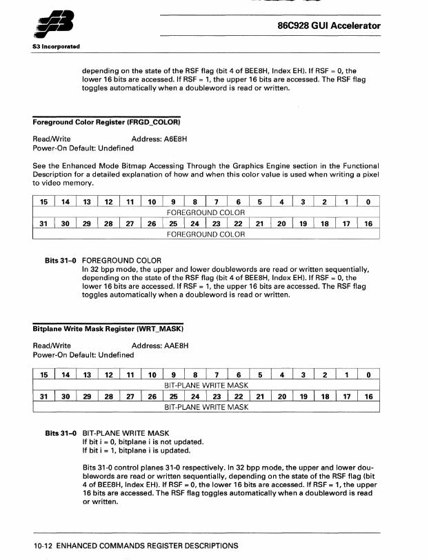
86C928 GUI Accelerator
S3 Incorporated
depending on the state of the RSF flag (bit 4 of BEE8H, Index EH). If RSF = 0, the lower 16 bits are accessed. If RSF = 1, the upper 16 bits are accessed. The RSF flag toggles automatically when a doubleword is read or written.
Foreground Color Register (FRGD_COLOR)
ReadIWrite Address: A6E8H Power-On Default: Undefined
See the Enhanced Mode Bitmap Accessing Through the Graphics Engine section in the Functional Description for a detailed explanation of how and when this color value is used when writing a pixel to video memory.
15 I 14 I 13 I 12 I 11 I 10 I 9 I 8 I 7 I 6 I 5 I 4 I 3 I 2 I 1 I 0
FOREGROUND COLOR
31 I 30 I 29 I 28 I 27 I 26 I 25 I 24 I 23 I 22 I 21 I 20 I 19 I 18 I 17 I 16
FOREGROUND COLOR
Bits 31-0 FOREGROUND COLOR In 32 bpp mode, the upper and lower doublewords are read or written sequentially, depending on the state of the RSF flag (bit 4 of BEE8H, Index EH). If RSF = 0, the lower 16 bits are accessed. If RSF = 1, the upper 16 bits are accessed. The RSF flag toggles automatically when a doubleword is read or written.
Bitplane Write Mask Register (WRT _MASK)
ReadIWrite Address: AAE8H Power-On Default: Undefined
15 I 14 I 13 I 12 I 11 I 10 I 9 I 8 I 7 I 6 I BIT-PLANE WRITE MASK
31 1~1~1~lvlul~lul~I~1 BIT-PLANE WRITE MASK
Bits 31-0 BIT-PLANE WRITE MASK If bit i = 0, bitplane i is not updated. If bit i = 1, bitplane i is updated.
5 I 4 I 3 121 1 I 0
21 I 20 I 19 I 18 I 17 I 16
Bits 31-0 control planes 31-0 respectively. In 32 bpp mode, the upper and lower doublewords are read or written sequentially, depending on the state of the RSF flag (bit 4 of BEE8H, Index EH). If RSF = 0, the lower 16 bits are accessed. If RSF = 1, the upper 16 bits are accessed. The RSF flag toggles automatically when a doubleword is read or written.
10-12 ENHANCED COMMANDS REGISTER DESCRIPTIONS
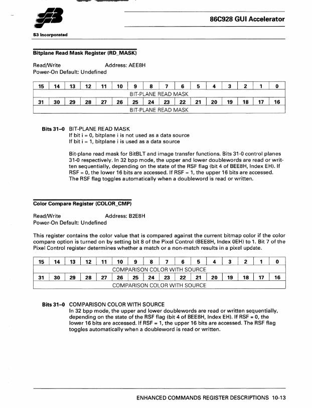
II· 86C928 GUI Accelerator
S3 Incorporated
Bitplane Read Mask Register (RD_MASK)
ReadIWrite Address: AEE8H Power-On Default: Undefined
15 I 14 I 13 I 12 I 11 I 10 I 9 I 8 I 7 I 6 I 51 4 I 3 I 2 I 1 I BIT-PLANE READ MASK
31 I 30 I 29 I 28 I 27 I 26 I 25 I 24 I 23 I 22 I 21 I 20 I 19 I 18 I 17 I BIT-PLANE READ MASK
Bits 31-0 BIT-PLANE READ MASK If bit i = 0, bitplane i is not used as a data source If bit i = 1, bitplane i is used as a data source
0
16
Bit-plane read mask for BitBLT and image transfer functions. Bits 31-0 control planes 31-0 respectively. In 32 bpp mode, the upper and lower doublewords are read or written sequentially, depending on the state of the RSF flag (bit 4 of BEE8H, Index EH). If RSF = 0, the lower 16 bits are accessed. If RSF = 1, the upper 16 bits are accessed. The RSF flag toggles automatically when a doubleword is read or written.
Color Compare Register (COLOR_CMP)
ReadIWrite Address: B2E8H Power-On Default: Undefined
This register contains the color value that is compared against the current bitmap color if the color compare option is turned on by setting bit 8 ofthe Pixel Control (BEE8H, Index OEH) to 1. Bit 7 ofthe Pixel Control register determines whether a match or a non-match results in a pixel update.
15 I 14 I 13 I 12 I 11 I 10 I 9 18 I 7 I 6 I 5 I 4 I 3 I 2 I 1 I 0 COMPARISON COLOR WITH SOURCE
31 I 30 I 29 J 28 I 27 I 26 I 25 I 24 J 23 I 22 I 21 I 20 I 19 I 18 I 17 I 16
COMPARISON COLOR WITH SOURCE
Bits 31-0 COMPARISON COLOR WITH SOURCE In 32 bpp mode, the upper and lower doublewords are read or written sequentially, depending on the state of the RSF flag (bit 4 of BEE8H, Index EH). If RSF = 0, the lower 16 bits are accessed. If RSF = 1, the upper 16 bits are accessed. The RSF flag toggles automatically when a doubleword is read or written.
ENHANCED COMMANDS REGISTER DESCRIPTIONS 10-13
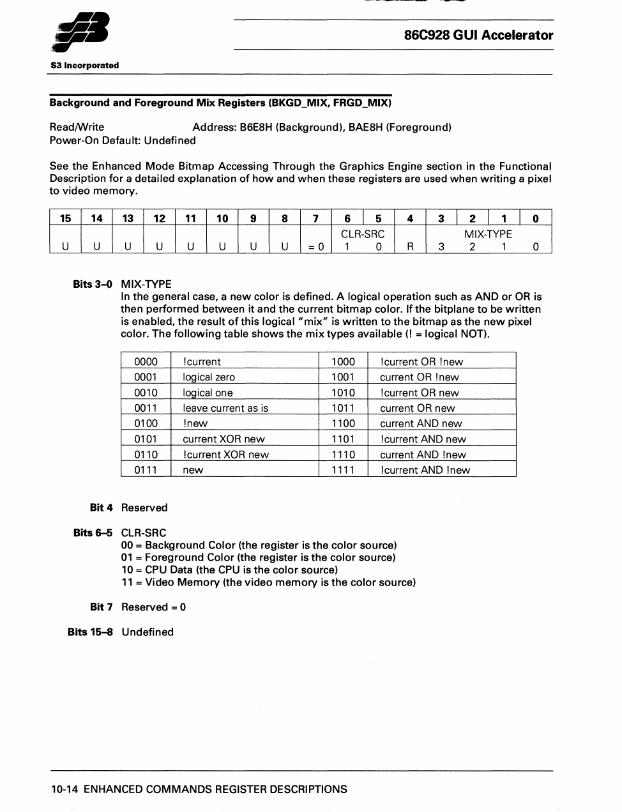
86C928 GUI Accelerator
S3 Incorporated
Background and Foreground Mix Registers (BKGD_MIX, FRGD_MIX)
Read/Write Address: B6E8H (Background), BAE8H (Foreground) Power-On Default: Undefined
See the Enhanced Mode Bitmap Accessing Through the Graphics Engine section in the Functional Description for a detailed explanation of how and when these registers are used when writing a pixel to video memory.
15
U
14 13 12 11 10 9 8 7 6 I 5 4 3 I 2 I 1 I 0
CLR-SRC MIX-TYPE U U U U U U U =0 1 0 R 3 2 1 0
Bits 3-0 MIX-TYPE In the general case, a new color is defined. A logical operation such as AND or OR is then performed between it and the current bitmap color. If the bitplane to be written is enabled, the result of this logical "mix" is written to the bitmap as the new pixel color. The following table shows the mix types available (! = logical NOT).
0000 !current 1000 !current OR !new
0001 logical zero 1001 current OR !new
0010 logical one 1010 !current OR new
0011 leave current as is 1011 current OR new
0100 !new 1100 current AND new
0101 current XOR new 1101 !current AND new
0110 !current XOR new 1110 current AND !new
0111 new 1111 !current AND !new
Bit 4 Reserved
Bits 6-5 CLR-SRC 00 = Background Color (the register is the color source) 01 = Foreground Color (the register is the color source) 10 = CPU Data (the CPU is the color source) 11 = Video Memory (the video memory is the color source)
Bit 7 Reserved = 0
Bits 15-8 Undefined
10-14 ENHANCED COMMANDS REGISTER DESCRIPTIONS
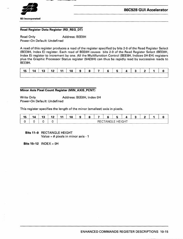
•-=. r S3 Incorporated
Read Register Data Register (RD_REG_DT)
Read Only Address: BEE8H Power-On Default: Undefined
86C928 GUI Accelerator
A read ofthis register produces a read of the register specified by bits 2-0 ofthe Read Register Select (BEE8H, Index E) register. Each read of BEE8H causes bits 2-0 of the Read Register Select (BEE8H, Index E) register to increment by one. All the Multifunction Control (BEE8H, Indices OH-EH) registers plus the Graphic Processor Status register (9AE8H) can thus be rapidly read by successive reads to BEE8H.
115 I 14 I 13 I 12 I 11 I 10 I 9 I 8 I 7 I 6 I 5 I 4 I 3 I 2 I 1 o
Minor Axis Pixel Count Register (MIN_AXIS_PCNT)
Write Only Address: BEE8H, Index OH Power-On Default: Undefined
This register specifies the length of the minor (smallest) axis in pixels.
Bits 11-0 RECTANGLE HEIGHT Value = # pixels in minor axis - 1
Bits 15-12 INDEX = OH
ENHANCED COMMANDS REGISTER DESCRIPTIONS 10-15
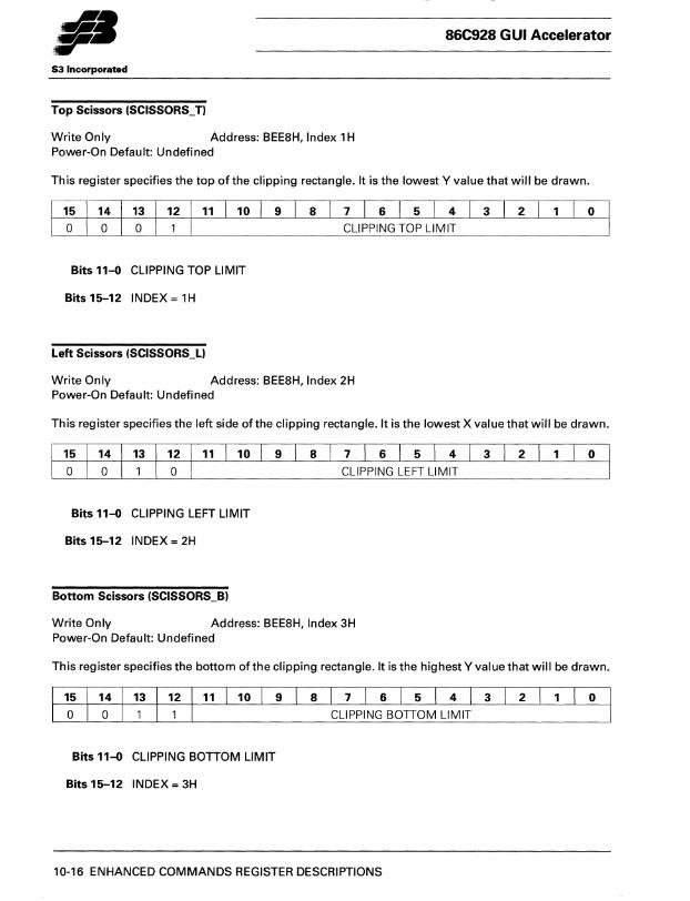
86C928 GUI Accelerator
53 Incorporated
Top Scissors (SCISSORS_T)
Write On Iy Address: BEE8H, Index 1 H Power-On Default: Undefined
This register specifies the top of the clipping rectangle. It is the lowest Y value that will be drawn.
Bits 11-0 CLIPPING TOP LIMIT
Bits 15-12 INDEX = 1H
Left Scissors (SCISSORS_L)
Write Only Address: BEE8H, Index 2H Power-On Default: Undefined
This register specifies the left side ofthe clipping rectangle. It is the lowest X value that will be drawn.
Bits 11-0 CLIPPING LEFT LIMIT
Bits 15-12 INDEX = 2H
Bottom Scissors (SCISSORS_B)
Write Only Address: BEE8H, Index 3H Power-On Default: Undefined
This register specifies the bottom of the clipping rectangle. It is the highest Yvalue that will be drawn.
Bits 11-0 CLIPPING BOTTOM LIMIT
Bits 15-12 INDEX = 3H
10-16 ENHANCED COMMANDS REGISTER DESCRIPTIONS
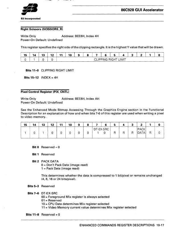
fl· 86C928 GUI Accelerator
S3 Incorporatad
Right Scissors (SCISSORS_R)
Write Only Address: BEE8H, Index 4H Power-On Default: Undefined
This register specifies the right side ofthe clipping rectangle. It is the highest Yvalue that will be drawn.
Bits 11-0 CLIPPING RIGHT LIMIT
Bits 15-12 INDEX = 4H
Pixel Control Register (PIX_CNTL)
Write Only Address: BEE8H, Index AH Power-On Default: Undefined
See the Enhanced Mode Bitmap Accessing Through the Graphics Engine section in the Functional Description for an explanation of how and when bits 7-6 ofthis register are used when writing a pixel to video memory.
15
1
14 13 12 11 10 9 8
0 1 0 0 0 0 0
Bit 0 Reserved = 0
Bit 1 Reserved
Bit 2 PACK DATA 0= Don't Pack Data (image read) 1 = Pack Data (image read)
7 I 6 5 4 3 2 1 0
DT-EX-SRC PACK 1 0 R R R DATA R 0
This determines whether the data is compressed to 1 bit/pixel or remains unchanged (4,8,16 or 24 bits/pixel).
Bits 5-3 Reserved
Bits 7-6 DT-EX-SRC 00 = Foreground Mix register is always selected 01 = Reserved 10 = CPU Data determines Mix register selected 11 = Video Memory current value determines Mix register selected
Bits 11-8 Reserved = 0
ENHANCED COMMANDS REGISTER DESCRIPTIONS 10-17
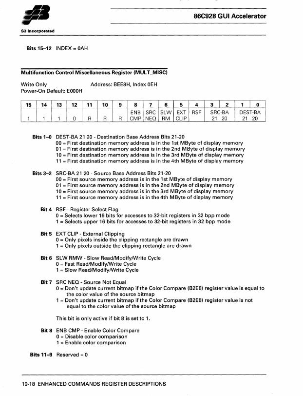
86C928 GUI Accelerator
S3 Incorporated
Bits 15-12 INDEX = OAH
Multifunction Control Miscellaneous Register (MUL T_MISC)
Write Only Address: BEE8H, Index OEH Power-On Default: EOOOH
15
1
14 13 12 11 10 9 8 7 6 5 4 3 I 2 1 I 0
ENB SRC SLW EXT RSF SRC-BA DEST-BA 1 1 0 R R R CMP NEQ RM CLIP 21 20 21
Bits 1-0 DEST-BA 21 20 - Destination Base Address Bits 21-20 00 = First destination memory address is in the 1st MByte of display memory 01 = First destination memory address is in the 2nd MByte of display memory 10 = First destination memory address is in the 3rd MByte of display memory 11 = First destination memory address is in the 4th MByte of display memory
Bits 3-2 SRC-BA 21 20 - Source Base Address Bits 21-20 00 = First source memory address is in the 1st MByte of display memory 01 = First source memory address is in the 2nd MByte of display memory 10 = First source memory address is in the 3rd MByte of display memory 11 = First source memory address is in the 4th MByte of display memory
Bit 4 RSF - Register Select Flag 0= Selects lower 16 bits for accesses to 32-bit registers in 32 bpp mode 1 = Selects upper 16 bits for accesses to 32-bit registers in 32 bpp mode
Bit 5 EXT CLIP - External Clipping 0= Only pixels inside the clipping rectangle are drawn 1 = Only pixels outside the clipping rectangle are drawn
Bit 6 SLW RMW - Slow Read/Modify/Write Cycle o = Fast Read/Modify/Write Cycle 1 = Slow Read/Modify/Write Cycle
Bit 7 SRC NEQ - Source Not Equal
20
0= Don't update current bitmap if the Color Compare (B2E8) register value is equal to the color value of the source bitmap
1 = Don't update current bitmap if the Color Compare (B2E8) register value is not equal to the color value ofthe source bitmap
This bit is only active if bit 8 is set to 1.
Bit 8 ENB CMP - Enable Color Compare o = Disable color comparison 1 = Enable color comparison
Bits 11-9 Reserved = 0
10~18 ENHANCED COMMANDS REGISTER DESCRIPTIONS
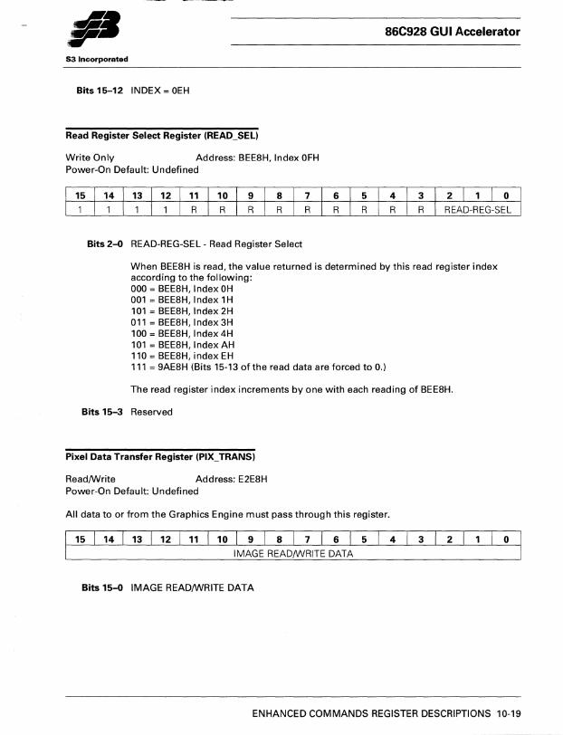
fl· 86C928 GUI Accelerator
53 Incorporated
Bits 15-12 INDEX = OEH
Read Register Select Register (READ_SEL)
Write Only Address: BEE8H, Index OFH Power-On Default: Undefined
Bits 2-0 READ-REG-SEL - Read Register Select
When BEE8H is read, the value returned is determined by this read register index according to the following: 000 = BEE8H, Index OH 001 = BEE8H, Index 1 H 101 = BEE8H, Index 2H 011 = BEE8H, Index 3H 100 = BEE8H, Index 4H 101 = BEE8H, Index AH 110 = BEE8H, index EH 111 = 9AE8H (Bits 15-13 of the read data are forced to 0.)
The read register index increments by one with each reading of BEE8H.
Bits 15-3 Reserved
Pixel Data Transfer Register (PIX_TRANS)
Read/Write Address: E2E8H Power-On Default: Undefined
All data to or from the Graphics Engine must pass through this register.
Bits 15-0 IMAGE READ/WRITE DATA
ENHANCED COMMANDS REGISTER DESCRIPTIONS 10-19
•• r 86C928 GUI Accelerator
53 Incorporated
Pixel Data Transfer - Extension Register IPIX_TRANS_EXTI
Read/Write Address: E2EAH Power-On Default: Undefined
This register is an extension of E2E8H for 32-bit operations.
Bits 15-0 IMAGE READ/WRITE DATA
10-20 ENHANCED COMMANDS REGISTER DESCRIPTIONS
86C928 GUI Accelerator
S3 Incorporated
Section 11: Enhanced Mode Programming
This section provides programming examples of Enhanced Mode features provided by the 86C928.
11.1 NOTATIONAL CONVENTIONS
The REGMNEMONIC on the left hand side of the arrow is the register mnemonic ofthe I/O port being written into. Text following a ';' is a comment.
REGMNEMONIC ¢= XXXXH REGMNEMONIC ¢= XXXXD REGMNEMONIC ¢= XXXX REGMNEMONIC ¢= XXXXXXXXXXXXXXXXB
; Load a hexadecimal value into the register. ; Load a decimal value into the register. ; Load a decimal value into the register ; Load a binary value into the register.
The programming examples often contain the following step:
wait for FIFO X empty
where X is some number between 1 and 8. This number equals the number of commands to follow that may need to be stored in the FIFO before execution. The number of empty FIFO entries is determined by reading bits [7:0] ofthe Graphics Processor Status (9AE8H, Read) register. These bits are interpreted as follows:
Bit i = 1 indicates all FIFO entries up to (i+1) are occupied. (FIFO entries are numbered 1-8.) Bit i = 0 indicates FIFO entry (i+1) and all higher entries are empty.
Thus, if you need 4 empty FIFO slots, you must ensure that bit 4 is cleared to O.
11.2 INITIAL SETUP
All examples assume the desired mode is selected. See Appendix A for the bit settings required for each mode. The video DAC must also be set up appropriately.
The Bitmap Access Through the Graphics Engine section of the Functional Description explains in detail how the colors, mixes and the data extensions are set for each example. These registers need not be set repeatedly before a series of draw commands if they use the same colors, mixes and data extension.
ENHANCED MODE PROGRAMMING 11-1
•• r 86C928 GUI Accelerator
S3 Incorporated
All bitmap updates are affected by the settings in the clipping registers (BEE8H, Indices 1-4) and the choice of internal or external clipping (BEE8H, Index E, bit 5). These must be set up so they include the area being drawn into.
If color compare is to be used, it must be enabled by setting bit 8 of the Multifunction Control Miscellaneous (BEE8H, Index OEH) register to 1. Bit 7 of this register determines whether a TRUE or FALSE comparison allows the pixel update to continue. The comparison color is programmed into the Color Compare (B2E8) register.
All planes are enabled for writing unless explicitly set otherwise in an example. This is done via the Write Mask (AAE8H) register.
11.3 PROGRAMMING EXAMPLES
This section provides programming examples for the following Enhanced Mode drawing operations:
• Solid Line
• Textured Line
• Rectangle
• Image Transfer Write-Through the Plane
• Image Transfer Write-Across the Plane
• Image Transfer Read-Through the Plane
• Image Transfer Read-Across the Plane
• BitBL T -Through the Plane
• BitBLT -Across the Plane
• Pattern Fill-Through the Plane
• Pattern Fill-Across the Plane
• Short Stroke Vectors
In addition, an example ofthe setup and programming of the hardware cursor is provided.
A number of programming steps are repeated in multiple examples. They are explained in detail at their first occurrence. Therefore, readers are encouraged to work through the examples from first to last.
11-2 ENHANCED MODE PROGRAMMING
86C928 GUI Accelerator
S3 Incorporated
11.3.1 Solid Line
Draw a solid line using axial coordinates from x1,y1 to x2,y2 using the mix NEW and color index 2.
Setup:
Drawing a line using axial coordinates requires programming the axial step constant into the Destination V-Position/Axial Step Constant (8AE8H) register (DESTV_AXSTP). the diagonal step constant into the Destination X-Position/Diagonal Step Constant (8EE8H) register (DESTX_DIASTP) and the error term into the Error Term (92E8H) register (ERR_TERM). Calculation of these three constants is based on the MAX and MIN parameters as calculated below.
MAX = maximum(ABS(x2-x1), ABS(y2-y1)) MIN = minimum(ABS(x2-x1), ABS(y2-y1))
where maximum means choose the largest of the two terms in parentheses and minimum means choose the smallest. ABS means take the absolute value ofthe expression.
Bits [7:5] of the Command (9AE8H) register (CMD) specify the drawing direction. Setting bit 7 to 1 means that the V drawing direction is positive (y1 < y2). Clearing bit 7 to 0 means the V drawing direction is negative (y1 > y2). Setting bit 6to 1 means that X isthe major (longer) axis (ABS(x2-x1) > ABS(y2-y1)). Clearing bit 6 to 0 means that V is the major axis. Setting bit 5 to 1 means that the X drawing direction is positive (x1 < x2). Clearing bit 5 to 0 means that the X drawing direction is negative (x1 > x2). These values replace the DDD sequence in the write to the CMD register shown in the pseudocode below.
The mix NEW represents a setting of 00111B in bits [4:0} of the Foreground Mix (BAE8H) register (FRGD_MIX). This overwrites the present bitmap color value with a new value.
The remainder of the setup is then:
Wait For FIFO 3 empty FRGD_MIX ¢= 0027H FRGD_COLOR ¢= 0002H MULTIFUNC_CNTL ¢= AOOOH
; Three commands to follow ; color source FRGD_COLOR, mix type is NEW ; color index ; Foreground Mix register provides color source and mix type
Drawing Operation:
Wait For FIFO 7 empty ; 7 commands to follow CUR_X ¢= x1 ; set starting horizontal position CUR_ V ¢= y1 ; set starting vertical position MAJ_AXIS_PCNT ¢= MAX ; length in pixels of the major axis DESTX_DIASTP ¢= 2 * (MIX-MAX) ; diagonal step constant DESTY_AXSTP ¢= 2 * MIN ; axial step constant If the X drawing direction is positive then
ERR_TERM ¢= 2 * MIN - MAX ; errorterm else ifthe X drawing direction is negative
ERR_TERM ¢= 2 * MIN - MAX -1 ; error term CMD ¢= 00100000DDD1 0011 B ; Draw line command (bits [15:13]), Draw (as opposed to
; just move ; current position)(bit 4), draw multiple pixels (bit 1). write (bit 0).
ENHANCED MODE PROGRAMMING 11-3
.... r 53 Incorporated
11.3.2 Textured Line
86C928 GUI Accelerator
Draw a textured line from x1,y1 to x2,y2 using the mix NEW for foreground mix, XOR for the background mix, foreground color index 2 and background color index4. The 16-bit line texture/pattern (PATTERN) is 0011000011110011B. When the pattern bit is a 1, the pixel is written with foreground color and mix. When the bit is a 0, the pixel is written with background color and mix.
Setup:
The XOR mix corresponds to a setting of 00101 B in bits [4:0] of the Background Mix (B6E8H) register (BKGD_MIX). See the Solid Line example for an explanation of other parameters and registers used in this example.
Wait For FIFO 5 empty FRGD_MIX ¢= 0027H FRGD_COLOR ¢= 0002H BKGD_MIX ¢= 0005H BKGD_COLOR ¢= 0002H MULTIFUNC_CNTL ¢= A080H
Drawing Operation:
; 5 commands to follow ; color source FRGD_COLOR, NEW mix type ; color index ; color source BKGD_COLOR, XOR mix type ; color index ; mask data selecting mix register provided by CPU
Wait For FIFO 7 empty ; 7 commands to follow CUR_X ¢= x1 ; set starting horizontal position CUR_ Y ¢= y1 ; set starting vertical position MAJ_AXIS_PCNT ¢= MAX ; length in pixels of major axis DESTX_DIASTP ¢= 2 * (MIX-MAX) ; diagonal step constant DE STY _AXSTP ¢= 2 * MIN ; axial step constant If the X drawing direction is positive then
ERR_TERM ¢= 2 * MIN - MAX ; error term else if the X drawing direction is negative
ERR_TERM ¢= 2 * MIN - MAX - 1 ; error term CMD ¢= 00100011DDD10011 B ; Draw line (bits [15:13]), 16-bit bus (bit 9), wait for data from the
; Pixel Transfer register (bit 8), Draw (bit 4), Multi-pixel (bit 1), ; Write (bit 0),
COUNT (of PATIERN words) = (MAX + 1 + 15)/16 PIX_TRANS ¢= 0011000011110011 B ; Output PATIERN to Pixel Transfer register COUNT times
An alternate faster method is:
COLOR_CMP ¢= 0011000011110011B ; This pattern is repeated an appropriate number of times to ; render the textured line.
11-4 ENHANCED MODE PROGRAMMING
86C928 GUI Accelerator
53 Incorporated
11 .3.3 Rectangle
Draw a rectangle with its top left corner at x1,y1, height = HEIGHT and width = WIDTH. Use the mix NEW and color index 2. The drawing direction (bits [7:5] in the write to the CMD register below) is set to X positive, X major and Y positive (111).
Setup:
Wait For FIFO 3 empty FRGD_MIX <= 0027H FRGD_COLOR <= 0002H MUL TIFUNC_CNTL <= AOOOH
Draw Operation:
Wait For FIFO 5 empty CUR_X <= x1 CUR_Y <=y1 MAJ_AXIS_PCNT <= WIDTH-1 MIN_AXIS_PCNT <= HEIGHT-1 CMD <= 0100000011110011 B
Note
; 3 commands to follow ; color source FRGD_COLOR, NEW mix type ; color index ; Foreground Mix register specifies color source and mix type
; 5 commands to follow ; set starting horizontal position ; set starting vertical position ; rectangle width ; rectangle height ; Draw rectangle (bits [15:13]), Draw (bit 4). Multi-pixel (bit 1), ; Write (bit 0)
The rectangle can be defined by specifying anyone ofthefourcorners and setting bits [7:5] accordingly. Always select X as the major axis (bit 6 =1).
Corner X direction (bit 5) Y direction (bit 7)
top left j)ositive (1) positive (1)
top right negative (0) positive (1)
bottom left positive (1) negative (0)
bottom right negative (0) negative (0)
ENHANCED MODE PROGRAMMING 11-5
86C928 GUI Accelerator
S3 Incorporated
11.3.4 Image Transfer Write-Through the Plane
A rectangular image is transferred from the CPU to the video memory through the planes. The image is stored as an array of pixels arranged in row majorfashion, in which a byte represents a pixel of data. While transferring in word (16-bit transfer) mode, the number of bytes transferred per row must be even-a dummy byte is added at row end if the width is odd. This example use a mix type of NEW and x1,y1 is the top left corner of the rectangle on the display. The height and width of the rectangle (in pixels) are HEIGHT and WIDTH.
Setup:
Wait For FIFO 5 empty FRGD_MIX_REG ¢= 0047H MULTIFUNC_CNTL ¢= AOOOH
Drawing Operation:
Wait For FIFO 2 empty CUR_X ¢= x1 CUR_Y ¢= y1 MAJ_AXIS_PCNT ¢= WIDTH-1 MIN_AXIS_PCNT ¢= HEIGHT-1 CMD ¢= 01010011D0110001 B
; 5 commands to follow ; color source CPU, mix type NEW ; Foreground Mix register is source for color source and mix type
; 2 commands to follow ; set starting horizontal position ; set starting vertical position ; rectangle width ; rectangle height ; Draw rectangle (bits [15:13]), Swap ON (bit 12), ; 16-bit transfers (bit 9), Wait for CPU data (bit 8). ; Always X Major (bit 6) & X Positive (bit 5), Draw (bit 4), ; Write (bit 0)
COUNT (of image pixel data to transfer) = ((WIDTH + 1 )/2)*HEIGHT words. PIX3RANS ¢= IMAGEDATA; Output image data to Pixel Transfer register for COUNT words.
Notes
In 4 bits/pixel mode, the image has to be packed so a single byte stores 2 pixels. The high nibble of a byte of data contains the nth pixel and the low nibble contains the (n + 1 )th pixel in a row. The row width has to be a multiple of 4, and rows have to be padded with up to 3 pixels of dummy data at each row end. COUNT (of image pixel data to transfer) = ((WIDTH +3)/4)*HEIGHT words.
The command in the above example specified 16 bits/pixel. If it had specified 8 bits/pixel, then for 8-plane modes, COUNT = (WIDTH * HEIGHT) bytes. For 4-plane modes, COUNT = ((WIDTH + 1 )/2 * HEIGHT) bytes. To output a byte, load the AL register with one byte and do OUT DX, AX.
11-6 ENHANCED MODE PROGRAMMING
86C928 GUI Accelerator
S3 Incorporated
11.3.5 Image Transfer Write-Across the Plane
A rectangular image is transferred from the CPU to the video memory across the plane. The monochrome bit image is stored as an array of pixels arranged in row majorfashion. A byte represents data for 8 pixels in a row. While using 16-bit transfers, the number of data bits transferred per row must be a multiple of 16-dummy bits are added at the row end if the width is not a multiple of 16. This example uses a mix type of NEW, and x1,y1 is the top left corner of the rectangle on the display. The height and width of the rectangle (in pixels) are HEIGHT and WIDTH. The monochrome image is translated so that pixels corresponding to a 1 in the bit image are given color index 4 and pixels corresponding to a 0 in the bit image are given color index O.
Setup:
Wait For FIFO 5 empty FRGD_MIX ¢= 0027H FRGD_COLOR ¢= 0004H BKGD_MIX ¢= 0007H BKGD_COLOR ¢= 0004H MUL TIFUNC_CNTL ¢= A080H
Drawing Operation:
Wait For FIFO 5 empty CUR_X ¢= x1 CUR_ Y ¢= y1 MAJ_AXIS_PCNT ¢= WIDTH-1 MIN_AXIS_PCNT ¢= HEIGHT-1 CMD ¢= 0101001100110011 B
; 5 commands to follow ; foreground color source, mix type NEW ; foreground color index 4 ; background color source, mix type NEW ; background color index 0 ; selection of mix register based on data from the CPU
; 5 commands to follow ; set starting horizontal position ; set starting vertical position ; rectangle width ; rectangle height ; Draw rectangle (bits [15:13]), Swap ON (bit 12), ; 16-bit transfers (bit 9)' Wait for CPU data (bit 8), ; Always X Major (bit 6) & X Positive (bit 5), Draw (bit 4), ; Multiple pixel (bit 1), Write (bit 0)
COUNT (of image pixel data to transfer) = ((WIDTH +15)/16)*HEIGHTwords PIX_TRANS ¢= IMAGEDATA; Output image data to Pixel Transfer register for COUNT words
Note
With 8-bit transfers, the number of data bits transferred per row must be a multiple of 8, so COUNT = ((WIDTH +7)/8)*HEIGHT bytes. To write to a single plane, set the foreground mix to 'logical one' (0002H), the background mix to 'logical zero' (0001 H), and the Write Mask register to select the desired (single) plane for updates.
ENHANCED MODE PROGRAMMING 11-7
86C928 GUI Accelerator
S3 Incorporated
11.3.6 Image Transfer Read-Through the Plane
A rectangular image is transferred from the video memory to the CPU. The image is read through the planes. The image is stored as an array of pixels arranged in row major fashion. A byte represents a pixel of data. While using 16-bit transfers, the number of bytes read per row must be even-a dummy byte is read at row end if the width is odd. For this example, x1,y1 is the top left corner of the rectangle on the display. The height and width of the rectangle (in pixels) are HEIGHT and WIDTH.
Setup:
Wait For FIFO 1 empty MULTIFUNC_CNTL <= AOOOH
Draw Operation:
Wait For FIFO 5 empty CUR_X <= x1 CUR_Y <= y1 MAJ_AXIS_PCNT <= WIDTH-1 MIN_AXIS_PCNT <= HEIGHT-1 CMD <= 0101001100110000B
Wait for Data Available
; 1 command to follow ; Foreground Mix register is the source of color source and ; mix type
; 5 commands to follow ; set starting horizontal position ; set starting vertical position ; rectangle width ; rectangle height ; Draw rectangle (bits [15:13]), Swap ON (bit 12), ; 16-bit transfers (bit 9), Wait for CPU data (bit 8), ; Always X Major (bit 6) & X Positive (bit 5), Draw (bit 4), ; Read (bit 0)
; bit 8 of the Graphics Processor Status (9AE8H, Read) ; register = 1
COUNT (of Image pixel data to read) = ((WIDTH + 1 )/2)*HEIGHT words IMAGEDATA <= PIX_ TRAN ; Input image data from Pixel Transfer register for COUNT words
Notes
In 4 bits/pixel mode, the image has to be packed so a single byte stores 2 pixels. The high nibble of a byte of data contains the nth pixel and the low nibble contains the (n + 1)th pixel in a row. The number of pixels read per row is a multiple of 4, and rows are padded with up to 3 pixels of dummy data at each row end. COUNT (of Image pixel data read) = ((WIDTH +3)/4)*HEIGHT words.
The command in the above example specified 16 bits/pixel. If it had specified 8 bits/pixel, then for 8-plane modes, COUNT = (WIDTH * HEIGHT) bytes. For 4-plane modes, COUNT = ((WIDTH + 1 )/2 * HEIGHT) bytes. To output a byte, load the AL register with one byte and do OUT OX.
11-8 ENHANCED MODE PROGRAMMING
•• r 86C928 GUI Accelerator
53 Incorporated
11.3.7 Image Transfer Read-Across the Plane
A rectangular monochrome image is transferred from the video memory to the CPU. Plane 0 is the source. The monochrome bit image is stored as an array of pixels arranged in row major fashion. A byte represents data for 8 pixels in a row. While using 16-bit transfers, the number of data bits read per row is a multiple of 16-dummy bits are read at row end if the width is not a multiple of 16. For this example, x1,y1 is the top left corner ofthe rectangle on the display. The height and width (in pixels) of the rectangle are HEIGHT and WIDTH.
Setup:
Wait For FIFO 2 empty MUL TIFUNC_CNTL <= AOCOH RD_MASK <= 01 H
Draw Operation:
Wait For FIFO 5 empty CUR_X <= x1 CUR_Y<=y1 MAJ_AXIS_PCNT <= WIDTH-1 MIN_AXIS_PCNT <= HEIGHT-1 CMD <= 0101001100110010B
Wait for Data Available
; 2 commands to follow ; data from video memory selects mix register ; read from plane 0
; 5 commands to follow ; set starting horizontal position ; set starting vertical position ; rectangle width ; rectangle height ; Draw rectangle (bits [15:13]), Swap ON (bit 12), ; 16-bit transfers (bit 9), Wait for CPU data (bit 8), ; Always X Major (bit 6) & X Positive (bit 5), Draw (bit 4), ; Multi-pixel (bit 1), Read (bit 0)
; bit 8 of the Graphics Processor Status (9AE8H, Read) ; reg ister = 1
COUNT (of image pixel data to transfer) = ((WIDTH +15)/16)*HEIGHTwords. IMAGEDATA <= PIX_TRANS ; Input image data from Pixel transfer register for COUNT words.
Note
With 8-bit transfers, the number of data bits transferred per row must be a multiple of 8, so COUNT = ((WIDTH +7)/8)*HEIGHT bytes. With more than 1 plane enabled for read, a '1' is read for the corresponding pixel if all planes enabled for reading are '1's. A '0' is read for the corresponding pixel if anyone of the planes enabled for reading is a '0'.
ENHANCED MODE PROGRAMMING 11-9
86C928 GUI Accelerator
S3 Incorporated
11.3.8 BitBL T -Through the Plane
A source rectangular area in video memory is transferred to a specified destination in video memory. The pixels are written into the destination rectangle using the current foreground mix. Assume x1,y1 is the top left corner of the source rectangle in video memory and x2,y2 is the top left corner of the destination rectangle. The rectangles could be overlapping or disjoint. The height and width (in pixels) of the rectangle are HEIGHT and WIDTH.
Setup:
First, the values of the Srcx, Srcy, Destx and Desty must be determined.
Case 1: Source and destination rectangles do not overlap
For X Positive, Y Positive: Srcx = x1, Srcy = y1, Destx = x2, Desty = y2
Case 2: Source and destination rectangles overlap
If x1 > x2 then if X Positive, Srcx = x1, Destx = x2
else Srcx = x1 - WIDTH -1, Desty = x2 - WIDTH-1 ; X Negative
Ify1 > y2 then if Y Positive, Srcy = y1, Desty = y2
else Srcy = y1 - HEIGHT -1, Desty = y2 - HEIGHT-1 ; Y Negative
Wait For FIFO 2 empty MULTIFUNC_CNTL ¢= AOOOH FRGD_MIX ¢= 0067H
Draw Operation:
Wait For FIFO 7 empty CUR_X ¢= Srcx CUR_ Y ¢= Srcy DESTX_DIASTP ¢= Destx DESTY _AXSTP ¢= Desty MAJ_AXIS_PCNT ¢= WIDTH-1 MIN_AXIS_PCNT ¢= HEIGHT-1 CMD ¢= 11000000DOD10011B
; 2 commands to follow ; Foreground Mix register is source of color source and mix type ; color source is video memory, mix type is NEW
; 7 commands to follow ; set starting horizontal position ; set starting vertical position ; set destination horizontal position ; set destination vertical position ; rectangle width ; rectangle height ; BitBL T (bits [15:13)), Always X Major (bit 6) , Draw (bit 4), ; MUlti-pixel (bit 1), Write (bit 0)
11-10 ENHANCED MODE PROGRAMMING
,I. 86C928 GUI Accelerator
S3 Incorporated
11.3.9 BitBL T -Across the Plane
A source rectangular area in video memory is transferred to a specified destination in display memory. The bits corresponding to a single plane specified by setting the Read Mask register can be transferred. With more than 1 plane enabled for read, if all the bits in the planes enabled for read are '1's then a '1' is read. If a bit in anyone of the planes enabled for read is a '0', then '0' is read. Assume x1,y1 is the top left corner of the source rectangle on the display, and x2,y2 is the top left corner of the destination rectangle. The image is read from plane 0 and written to plane 2. The rectangles could be overlapping or disjoint. The height and width (in pixels) ofthe rectangle are HEIGHT and WIDTH.
,Setup:
First, the values of the Srcx, Srcy, Destx and Desty must be determined.
Case 1: Source and destination rectangles do not overlap
For X Positive, Y Positive: Srcx = x1, Srcy = y1, Destx = x2, Desty = y2
Case 2: Source and destination rectangles overlap
If x1 > x2 then if X Positive, Srcx =x1, Destx = x2
else Srcx = x1 - WIDTH -1, Desty = x2 - WIDTH-1 ; X Negative
If y1 > y2 then if Y Positive, Srcy = y1, Desty = y2
else Srcy = y1 - HEIGHT -1, Desty = y2 - HEIGHT-1 ; Y Negative
Wait For FIFO 5 empty MULTIFUNC_CNTL ¢= AOCOH FRGD_MIX ¢= 0002H BKGD_MIX ¢= 0001 H RD_MASK ¢= 0001 H WRT _MASK ¢= 0004H
Draw Operation:
Wait For FIFO 7 empty CUR_X ¢= Srcx CUR_ Y ¢= Srcy DESTX_DIASTP ¢= Destx DESTY _AXSTP ¢= Desty MAJ_AXIS_PCNT ¢= WIDTH-1 MIN_AXIS_PCNT ¢= HEIGHT-1 CM D ¢= 11 000000DOD1 0011 B
; 5 commands to follow ; data from video memory selects mix register ; Always 'logical l' ; Always 'logical 0' ; Read from plane 0 ; Plane 2 enabled for write
; 7 commands to follow ; set starting horizontal position ; set starting vertical position ; set destination horizontal position ; set destination vertical position ; rectangle width ; rectangle height ; BitBL T (bits [15:13]), Always X Major (bit 6) , Draw (bit 4), ; Mu Iti-pixel (bit 1), Write (bit 0)
ENHANCED MODE PROGRAMMING 11-11
86C928 GUI Accelerator
S3 Incorporated
Note
It is possible to translate a monochrome image, e.g., text fonts, stored ina single plane in video memory into a 2-color image. This is accomplished by setting the mix registers differently and setting the desired background and foreground colors. If the source bit is a '1', then the corresponding pixel at the destination is colored with the foreground color index. The destination pixel is colored with the background color index if the corresponding source bit is a '0'. The setup for this is as follows:
FRGD_MIX ¢= 0027H BKGD_MIX ¢= 0007H FRGD_COLOR ¢= 0004H BKGD_COLOR ¢= 0001H
; color source foreground, mix type NEW ; color source background, mix type NEW ; foreground color ; background color
11-12 ENHANCED MODE PROGRAMMING
86C928 GUI Accelerator
83 Incorporated
11.3.10 PatBl T -Pattern Fill Through the Plane
An 8x8 pixel pattern is initially copied into video memory using an image transfer operation. This source pattern is then repeatedly copied to a destination rectangle of arbitrary size. Each copy is aligned to an 8-pixel boundary. The pixels are written into the destination rectangle using the current foreground mix. Assume x1,y1 is the top left corner of the source rectangle on the display and x2,y2 is the top left corner of the destination rectangle. The height and width (in pixels) of the rectangle are HEIGHT and WIDTH.
Setup:
Wait For FIFO 2 empty MUL TIFUNC_CNTL ¢= AOOOH FRGD_MIX ¢= 0067H
Draw Operation
Wait For FIFO 7 empty CUR_X ¢= x1 CUR_Y¢=y1 DESTX_DIASTP ¢= x2 DESTY _AXSTP ¢= y2 MAJ_AXIS_PCNT ¢= WIDTH-1 MIN_AXIS_PCNT ¢= HEIGHT-1 CMD ¢= 111 00000DOD10011 B
Note
; 2 commands to follow ; Foreground Mix register is source of color source and mix type ; color source is video memory, mix type is NEW
; 7 commands to follow ; set starting horizontal position ; set starting vertical position ; set destination horizontal position ; set destination vertical position ; rectangle width ; rectangle height ; Pattern Fill (bits [15:13]), Always X Major (bit 6) , Draw (bit 4), ; Multi-pixel (bit 1), Write (bit 0)
The X coordinate of the source rectangle must be on an 8 pixel boundary (x=O, x=8, etc.). This pattern should be located in the non-displayed area of the bitmap. The source X destination patterns should be non-overlapping.
ENHANCED MODE PROGRAMMING 11-13
86C928 GUI Accelerator
S3 Incorporated
11.3.11 PatBl T -Pattern Fill Across the Plane
An 8x8 pixel pattern is initially copied into video memory using an image transfer operation. This source pattern is then transferred to a specified destination in video memory. The bits corresponding to a single plane specified by setting the Read Mask register can be transferred. With more than 1 plane enabled for read, if all the bits in the planes enabled for read are '1 's, then a '1' is read. If a bit in any one of the planes enabled for read is a '0', then '0' is read. Assume x1.y1 is the top left corner of the source rectangle on the display, and x2.y2 is the top left corner ofthe destination rectangle. The image is read from plane 0 and written to plane 2. The height and width of the rectangle are HEIGHT and WIDTH.
Setup:
Wait For FIFO 5 empty MULTIFUNC_CNTL ~ AOCOH FRGD_MIX ~ 0002H BKGD_MIX ~ 0001 H RD_MASK ~ 0001 H WRT _MASK ~ 0004H
Draw Operation:
Wait For FIFO 7 empty CUR_X ~x1 CUR_Y ~ y1 DESTX_DIASTP ~ x2 DESTY _AXSTP ~ y2 MAJ_AXIS_PCNT ~ WIDTH-1 MIN_AXIS_PCNT ~ HEIGHT-1 CMD ~ 11100000DOD10011B
Notes
; 5 commands to follow ; data from video memory selects mix register ; Always 'logical l' ; Always 'logical 0' ; Read from plane 0 ; Plane 2 enabled for write
; 7 commands to follow ; set starting horizontal position ; set starting vertical position ; set destination horizontal position ; set destination vertical position ; rectangle width ; rectangle height ; Pattern Fill (bits [15:13]), Always X Major (bit 6) ,Draw (bit 4), ; Multi-pixel (bit 1), Write (bit 0)
The X coordinate ofthe source rectangle must be on an 8 pixel boundary (x=O, x=8, etc.). This pattern should be located in the non-displayed area of the bitmap. The source X destination patterns should be non-overlapping.
To expand the source mono pattern into a 2-color pattern, set the foreground mix to 27H, the background mix to 7H and the foreground and background colors as desired. Also set the write mask to FFH.
11-14 ENHANCED MODE PROGRAMMING
86C928 GUI Accelerator
S3 Incorporated
11.3.12 Short Stroke Vectors
Using short stroke vectors, short lines up to 15 pixels in length can be drawn rapidly because it is not necessary to calculate and set the line constants. Such lines are constrained to one of the 8 directions at 45 degree increments starting at 0 degrees. The current point x1,y1 is set and a NOP command is issued to set all the desired drawing parameters without actually writing a pixel. For example, bit 2 (Last Pixel Off) would be set to 1 (OFF) for drawing connected lines until the last line is drawn. The short stroke vector parameters are then loaded in the Short Stroke Vector Transfer (9EE8H) register (SHORT_STROKE). Two vectors can be defined at a time, one in the low byte and one in the high byte. For the low byte, bits [7:5] define the direction, with bit 4 set to '1' for a draw operation or to '0' for a move current position operation. Bits [3:0] define the length of the short line. Let SSVDO, SSVD1, ... SSVDN-1 bytes be the short stroke vector data for N lines.
Setup:
Wait For FIFO 3 empty MULTIFUNC_CNTL <= AOOOH FRGD_MIX <= 0027H FRGD_COLOR <= 0004H
Draw Operation:
CUR_X <= xl CUR_Y <= y1 CMD <= 0001001 OXXX11111 B
While space available in the FIFO
; 3 commands to follow ; Foreground Mix register is source of color source and mix type ; use foreground color, mix type NEW ; foreground color index 4
; set starting horizontal position ; set starting vertical position ; NOP (bits [15:13]), Byte Swap (bit 12), 16-bit transfers (bit 9) , ; Draw (bit 4), RadialDir (bit 3), LPixelOff (bit 2), Multi-pixel (bit 1), ; Write (bit 0)
SHORLSTROKE <= SSVD1 SHL 8 + SSVDO ; SSVD1 shifted to high byte, SSVDO in low byte SHORT_STROKE <= SSVD3 SHL 8 + SSVD2 ; Byte swap turned on to read vectors out in
; correct order
SHORT_STROKE <= SSVDN-1 SHL 8 + SSVDN-2
ENHANCED MODE PROGRAMMING 11-15
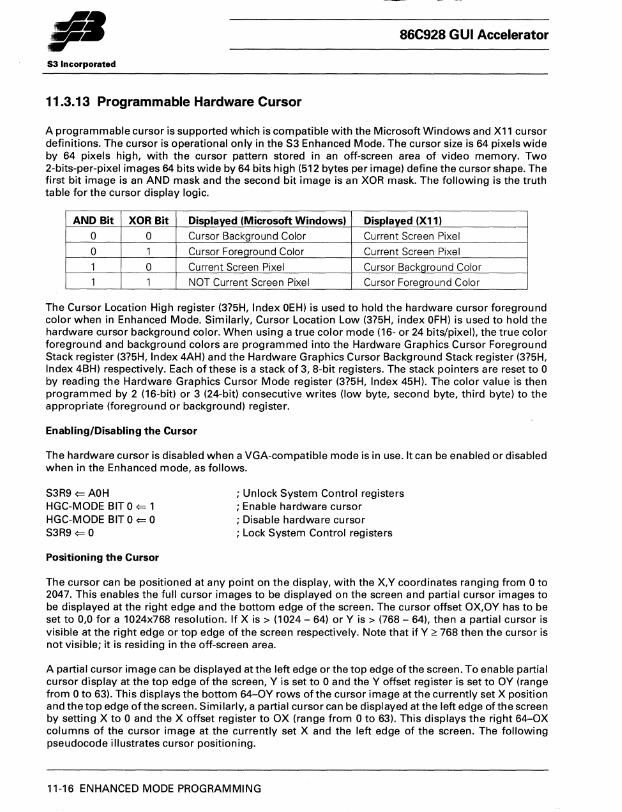
86C928 GUI Accelerator
53 Incorporated
11.3.13 Programmable Hardware Cursor
A programmable cursor is supported which iscompatible with the Microsoft Windows and X11 cursor definitions. The cursor is operational only in the S3 Enhanced Mode. The cursor size is 64 pixels wide by 64 pixels high, with the cursor pattern stored in an off-screen area of video memory. Two 2-bits-per-pixel images 64 bits wide by 64 bits high (512 bytes per image) define the cursor shape. The first bit image is an AND mask and the second bit image is an XOR mask. The following is the truth table for the cursor display logic.
AND Bit XOR Bit Displayed (Microsoft Windows) Displayed (X11)
0 0 Cursor Background Color Current Screen Pixel
0 1 Cursor Foreground Color Current Screen Pixel
1 0 Current Screen Pixel Cursor Background Color
1 1 NOT Current Screen Pixel Cursor Foreground Color
The Cursor Location High register (3?5H, Index OEH) is used to hold the hardware cursor foreground color when in Enhanced Mode. Similarly, Cursor Location Low (3?5H, index OFH) is used to hold the hardware cursor background color. When using a true color mode (16- or 24 bits/pixel), the true color foreground and background colors are programmed into the Hardware Graphics Cursor Foreground Stack register (3?5H, Index 4AH) and the Hardware Graphics Cursor Background Stack register (3?5H, Index 4BH) respectively. Each of these is a stack of 3, 8-bit registers. The stack pointers are reset to 0 by reading the Hardware Graphics Cursor Mode register (3?5H, Index 45H). The color value is then programmed by 2 (16-bit) or 3 (24-bit) consecutive writes (low byte, second byte, third byte) to the appropriate (foreground or background) register.
Enabling/Disabling the Cursor
The hardware cursor is disabled when a VGA-compatible mode is in use. It can be enabled or disabled when in the Enhanced mode, as follows.
S3R9 ¢= AOH HGC-MODE BIT 0 ¢= 1 HGC-MODE BIT 0 ¢= 0 S3R9 ¢= 0
Positioning the Cursor
; Unlock System Control registers ; Enable hardware cursor ; Disable hardware cursor ; Lock System Control registers
The cursor can be positioned at any point on the display, with the X,V coordinates ranging from 0 to 2047. This enables the full cursor images to be displayed on the screen and partial cursor images to be displayed at the right edge and the bottom edge of the screen. The cursor offset OX,OV has to be set to 0,0 for a 1024x768 resolution. If X is > (1024 - 64) or V is > (768 - 64), then a partial cursor is visible at the right edge or top edge of the screen respectively. Note that if V ~ 768 then the cursor is not visible; it is residing in the off-screen area.
A partial cursor image can be displayed at the left edge or the top edge of the screen. To enable partial cursor display at the top edge of the screen, V is set to 0 and the V offset register is set to OV (range from 0 to 63). This displays the bottom 64-0V rows of the cursor image at the currently set X position and the top edge ofthe screen. Similarly, a partial cursor can be displayed at the left edge ofthe screen by setting X to 0 and the X offset register to OX (range from 0 to 63). This displays the right 64-0X columns of the cursor image at the currently set X and the left edge of the screen. The following pseudocode illustrates cursor positioning.
11-16 ENHANCED MODE PROGRAMMING
. .lJa ,.. 53 Incorporated
S3R9 ~AOH HWGC-CX(H) ~ MS 3 bits of X cursor position HWGC-CX(L) ~ LS 8 bits of X cursor position HWGC-CV(L) ~ LS 8 bits of V cursor position HWGC-DX ~ Cursor Offset X position HWGC-DV ~ Cursor Offset V position HWGC-CV(H) ~ MS 3 bits of V cursor position S3R9 ~ 0
Programming the Cursor Shape
86C928 GUI Accelerator
; Unlock System Control registers ; bits [10:8] ; bits [7:0] ; bits [7:0] ; bits [5:0] ; bits [5:0] ; bits [10:8] ; Lock System Control registers
TheANO and the XOR images are 512 bytes each. The cursor image bitmaps are loaded into the display bitmap at some V location (VI) in the off-screen area and start X is set at O. This cursor pattern load is accomplished by performing an image transfer operation with the destination rectangle on the display set to O,VI, the width set to 1024, and height set to 1 (2 if the 4 plane option is being used). The AND and XOR image bitmaps are transferred to the video memory via the Pixel Data Transfer (E2E8H) register. The image is loaded into the register as a sequence of AND image mask words followed by a word of the XOR image mask. This alternation is continued until the entire cursor pattern is loaded. The Hardware Graphics Cursor (3?5H, Indices 4CH and 4DH) registers are programmed to VI so the controller knows the start ofthe cursor definition in video memory. The X location is always assumed to be O.
The AND_IMAGE is defined by the 256 words ANDwordO, ANDword1, ... ANDword255 and the XOR_IMAGE is defined by the 256 words XORwordO, XORword1, ... XORword255.
Setup:
S3R9 ~ AOH ; Unlock System Control registers HWGC-STA(H) ~ MS 4 bits ofthe cursor storage V start = VI (bits [11:8]) HWGC-STA(L) ~ LS 8 bits of the cursor storage V start = Vl(bits [7:0]) S3R9 ~ 0 ; Lock System Control registers
Wait for FIFO 7 empty MULTIFUNC_CNTL ~ AOOOH FRGD_MIX ~ 47H
Draw Operation:
; Foreground Mix register is source of color source and mix type ; color source is CPU, mix type NEW
CUR_X ~ 0; set starting horizontal position CUR_ V ~ V1 ; set starting vertical position, which should be in the
MAJ_AXIS_PCNT ~ (1024-1) MIN_AXIS_PCNT ~ (1-1) CMD ~ 0101001111010001 B
; off-screen area ; rectangle width ; rectangle height ; Rectangle Fill (bits [15:13]). Byte Swap (bit 12). ; 16-bit bus (bit 9), Draw (bit 4). Write (bit 0)
ENHANCED MODE PROGRAMMING 11-17
fl· 53 Incorporated
While FIFO space available PIX_TRANS ¢= ANDwordO, XORwordO PIX_TRANS ¢= ANDword1, XORword1
PIX_TRANS ¢= ANDword255, XORword255
Notes
86C928 GUI Accelerator
I/O operations to the registers used to program the cursor and set up Extended Mode are byte transactions. To write to these registers, an index is written at the I/O port 3?4H (? = D for color or B for monochrome) and the data is written to I/O port 3?5H.
If the cursor is not 64 bits by 64 bits, the given images should be padded to make the cursor image 64 bits by 64 bits. The padded area should be made transparent by padding the extra AND mask bits with '1's and the extra XOR bits by 'O's.
For the 4-plane mode with 0.5 MByte memory option, the cursor pattern is stored in the off-screen video memory in a rectangle of width 1024 and height 2. For the 4-plane mode with 1 MByte memory option, the cursor pattern is stored in the off-screen video memory in a rectangle of width 2048 and height 1. In all cases the clipping rectangle should be set to include the cursor<:tefinition rectangle prior to loading the cursor image.
The cursor can be programmed to 64 bits by 64 bits in all modes, including the 16 and 24 bits/pixel true color modes. When a 2x or 3x zoom is selected by setting bit 2 or bit 3 respectively in the Hardware Graphics Cursor Mode (3?5H, Index 45H) register, the colors are automatically taken from the Hardware Graphics Cursor Foreground Stack (3?5H, Index 4A) and the Hardware Graphics Cursor Background Stack (3?5H, Index 4B).
11-18 ENHANCED MODE PROGRAMMING
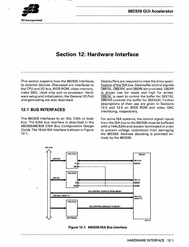
86C928 GUI Accelerator
S3 Incorporated
Section 12: Hardware Interface
This section explains how the 86C928 interfaces to external devices. Discussed are interfaces to the CPU and I/O bus, BIOS ROM, video memory, video DAC, clock chip and co-processor. Hardware setup and initialization, the General I/O Port and genlocking are also described.
12.1 BUS INTERFACES
The 86C928 interfaces to an ISA, EISA or local bus. The EISA bus interface is described in the 86C805/86C928 EISA Bus Configuration Design Guide. The 16-bit ISA interface is shown in Figure 12-1.
ISABUS
/' '74Ai:S'245
80[15:8J
G OIR
'------
'74Ai:S'245 80[7:0]
G
OIR '------
Data buffers are required to meet the drive specification ofthe ISA bus. Data buffer control signals DBENL, DBENH, and DBDIR are provided. DBDIR is driven low for reads and high for writes. DBENL is used to control the buffer for SD[7:0]. DBENH controls the buffer for SD[15:8]. Further descriptions of their use are given in Sections 12.3 and 12.5 on BIOS ROM and video DAC interfacing, respectively.
For some ISA systems, the control signal inputs from the ISA bus to the 86C928 must be buffered with a 74ALS244 and resistor terminated in order to prevent voltage undershoot from damaging the 86C928. Address decoding is provided entirely by the 86C928.
.. CO2.
80[15:8J
DBENH
SOI',O]
DBENL
DBOIR
ISA CONTROL SIGNALS FROM 86C801
SA[16:0], LA[23:17] SA[16:o1 LA[23:17)
~
ISA CONTROL SIGNALS TO 86C801
V iOPTiiiNAi:i 3001120
Figure 12-1. 86C928/ISA Bus Interface
HARDWARE INTERFACE 12-1
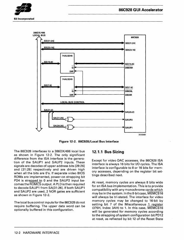
•• r 53 Incorporated
860X/486 3 LO CA BUS
"" S0131:24J
SO[23:16J
SO[15:1IJ
SO[7:0J
74ALS245
-
G
OIR I--
74ALS245
G
OIR
LOCAL BUS CONTROL
SA[31:2J
[SA[31:2~ SA[28:26J
7'
86C928 GUI Accelerator
86C928
S0131:24J
SO[23:16J
SO[15:8J
OBENH
SO[7:0J
OBENL
OBOIR
SA[25:2J
SAUP2
SAUPI
3000660
Figure 12-2. 86C928/Local Bus Interface
The 86C928 interfaces to a 386DX/486 local bus as shown in Figure 12-2. The only significant difference from the ISA interface is the generation of the SAUP1 and SAUP2 inputs. These signals are decodes of upper address ~its [28:~6] and [31:29] respectively and are driven high when all the bits are O's. If separati:l video BIOS ROMs are implemented, power-on strapping bit PD4 is str~ 0 and the SAUP2 input becomes the ROMCS output. A PLD is then required to decode SAUP1 from SA[31 :26]. If both SAUP1 and SAUP2 are used, 2 NOR gates are sufficient as shown in Figure 12-2.
The local bus control inputs forthe 86C928 do not require buffering. The upper data word can be optionally buffered in this configuration.
12-2 HARDWARE INTERFACE
12.1.1 Bus Sizing
Except for video DAC accesses, the 86C928 ISA interface is always 16 bits for I/O cycles. The ISA interface is configurable to 8 or 16 bits for memory accesses, depending on the register bit settings described next.
At reset, memory cycles are always 8 bits wide for an ISA bus implementation. This isto provide compatibility with any monochrome cards which may be in the system. In the 8-bitcase, MEMCS16 will always be tri-stated. The interface for video memory cycles may be changed to 16-bit by setting bit 7 of the Miscellaneous 1 register (3?5H, Index 3AH) to 1. In this case, MEMCS16 will be generated for memory cycles according to the strappi ng of system configuration bit PD12 at reset, as reflected by bit 12 of the Reset State
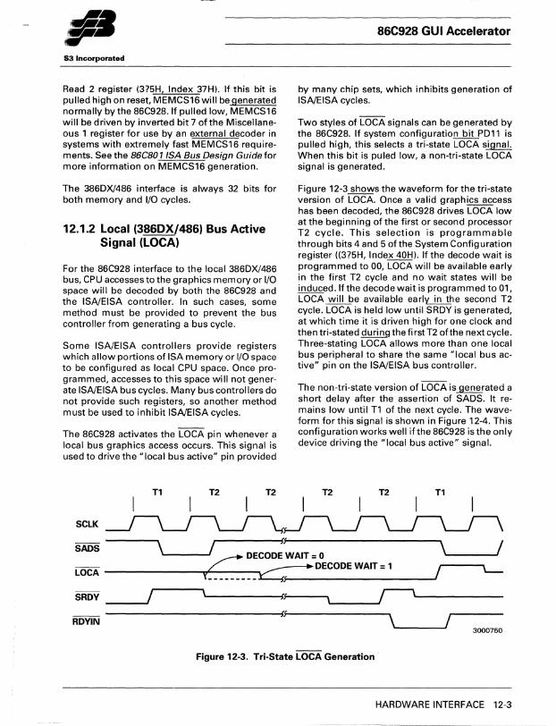
S3 Incorporated
Read 2 register (3?5H, Index 37H). If this bit is pulled high on reset, MEMCS16 will be generated normally by the 86C928.lf pulled low, MEMCS16 will be d riven by inverted bit 7 of the Miscellaneous 1 register for use by an external decoder in systems with extremely fast MEMCS16 requirements. See the 86C80 1 ISA Bus Design Guide for more information on MEMCS16 generation.
The 386DX/486 interface is always 32 bits for both memory and I/O cycles.
12.1.2 Local (386DX/486) Bus Active Signal (LOCA)
For the 86C928 interface to the local 386DX/486 bus, CPU accesses to the graphics memory or I/O space will be decoded by both the 86C928 and the ISNEISA controller. In such cases, some method must be provided to prevent the bus controller from generating a bus cycle.
Some ISA/EISA controllers provide registers which allow portions of ISA memory or I/O space to be configured as local CPU space. Once programmed, accesses to this space will not generate ISNEISA bus cycles. Many bus controllers do not provide such registers, so another method must be used to inhibit ISNEISA cycles.
The 86C928 activates the LOCA pin whenever a local bus graphics access occurs. This signal is used to drive the "local bus active" pin provided
T1 T2 T2
SCLK
86C928 GUI Accelerator
by many chip sets, which inhibits generation of ISNEISA cycles.
Two styles of LOCA signals can be generated by the 86C928. If system configu ration bit PD11 is pulled high, this selects a tri-state LOCA signal. When this bit is puled low, a non-tri-state LOCA signal is generated.
Figure 12-3 shows the waveform for the tri-state version of LOCA. Once a valid graphics access has been decoded, the 86C928 drives LOCA low at the beginning of the first or second processor T2 cycle. This selection is programmable through bits 4 and 5 ofthe System Configuration register ((3?5H, Index 40H). 1ft he decode wait is programmed to 00, LOCA will be available early in the first T2 cycle and no wait states will be induced. If the decode wait is programmed to 01, LOCA will be available earl'Ll!!...!..he second T2 cycle. LOCA is held low until SRDY is generated, at which time it is driven high for one clock and then tri-stated during the fi rst T2 ofthe next cycle. Three-stating LOCA allows more than one local bus peripheral to share the same "local bus active" pin on the ISNEISA bus controller.
The non-tri-state version of LOCA is generated a short delay after the assertion of SADS. It remains low until T1 of the next cycle. The waveform for this signal is shown in Figure 12-4. This configuration works well ifthe 86C928 is the only device driving the "local bus active" signal.
T2 T2 T1
\'------'/ ..--. DECOD::WAIT = 0
LOCA -------........ V('""_-_-_-_-__ -_---,_ ~ DECODE WAIT = 1
SADS \'--_--11 , SRDY _--I,,--'------Juf---'-___ I''-------
\'-_--J/ RDYIN 3000750
Figure 12-3. Tri-State LOCA Generation
HARDWARE INTERFACE 12-3
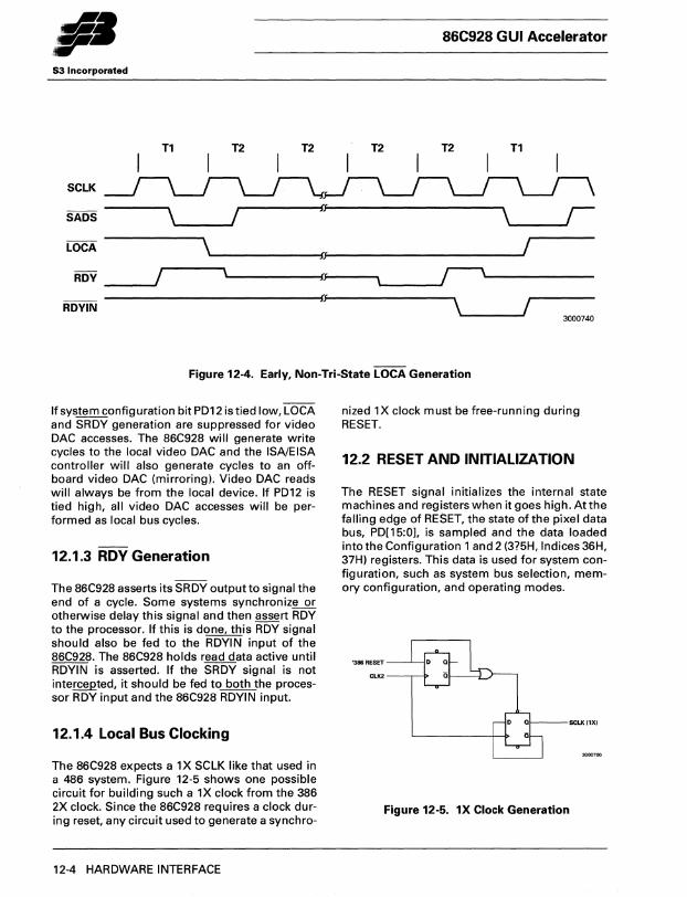
86C928 GUI Accelerator
53 Incorporated
T1 T2 T2 T2 T2 11
SCLK
SADS \ I \ I LOCA \ ,fo /
RDY / :f I' :f \ / RDYIN
3000740
Figure 12-4. Early, Non-Tri-State LOCA Generation
If system configuration bit PD12 is tied low, LOCA and SRDY generation are suppressed for video DAC accesses. The 86C928 will generate write cycles to the local video DAC and the ISNEISA controller will also generate cycles to an offboard video DAC (mirroring). Video DAC reads will always be from the local device. If PD12 is tied high, all video DAC accesses will be performed as local bus cycles.
12.1.3 RDY Generation
The 86C928 asserts its SRDY output to signal the end of a cycle. Some systems synchronize or otherwise delay this signal and then assert RDY to the processor. If this is done, this RDY signal should also be fed to the RDYIN input of the 86C928. The 86C928 holds read data active until RDYIN is asserted. If the SRDY signal is not intercepted, it should be fed to both the processor RDY input and the 86C928 RDYIN input.
12.1.4 Local Bus Clocking
The 86C928 expects a 1X SCLK like that used in a 486 system. Figure 12-5 shows one possible circuit for building such a 1X clock from the 386 2X clock. Since the 86C928 requires a clock during reset, any circuit used to generate a synchro-
12-4 HARDWARE INTERFACE
nized 1X clock must be free-running during RESET.
12.2 RESET AND INITIALIZATION
The RESET signal initializes the internal state machines and registers when it goes high. At the falling edge of RESET, the state of the pixel data bus, PD[15:0], is sampled and the data loaded into the Configuration 1 and 2 (3?5H, Indices 36H, 37H) registers. This data is used for system configuration, such as system bus selection, memory configuration, and operating modes.
'386 RESET
CLK2
SCLK (1X)
Figure 12-5. 1X Clock Generation
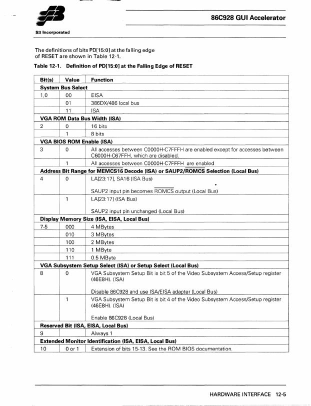
II· S3 Incorporated
The definitions of bits PD[15:0] at the falling edge of RESET are shown in Table 12-1.
Table 12-1. Definition of PD[15:0] at the Falling Edge of RESET
Bit(s) Value Function
System Bus Select
1,0 00 EISA
01 386DX/486 local bus
11 ISA
VGA ROM Data Bus Width (lSA)
2 0 16 bits
1 8 bits
VGA BIOS ROM Enable (lSA)
86C928 GUI Accelerator
3 0 All accesses between COOOOH-C7FFFH are enabled except for accesses between C6000H-C67FFH, which are disabled.
1 All accesses between COOOOH-C7FFFH are enabled
Address Bit Range for MEMCS16 Decode (lSA) or SAUP2/ROMCS Selection (Local Bus)
4 0 LA[23:17J, SA16 (ISA Bus) . ---
SAUP2 input pin becomes ROMCS output (Local Bus)
1 LA[23:17] (lSA Bus)
SAUP2 input pin unchanged (Local Bus)
Display Memory Size (lSA, EISA, Local Bus)
7-5 000 4 MBytes
010 3 MBytes
100 2 MBytes
110 1 MByte
111 0.5 MByte
VGA Subsystem Setup Select (lSA) or Setup Select (Local Bus)
8 0 VGA Subsystem Setup Bit is bit 5 of the Video Subsystem Access/Setup register (46E8H). (ISA)
Disable 86C928 and use ISA/EISA adapter (Local Bus)
1 VGA Subsystem Setup Bit is bit 4 of the Video Subsystem Access/Setup register (46E8H). (ISA)
Enable 86C928 (Local Bus)
Reserved Bit (lSA, EISA, Local Bus)
9 Always 1
Extended Monitor Identification (lSA, EISA, Local Bus)
10 o or 1 Extension of bits 15-13. See the ROM BIOS documentation.
HARDWARE INTERFACE 12-5
86C928 GUI Accelerator
53 Incorporatad
Table 12-1. Definition of PD[15:0] atthe Falling Edge of RESET (Continued)
Bit(s) Value Function
No Wait State liSA) or LOCA type (Local Bus)
11 0 NOWS disabled (ISA)
LOCA is a level signal (Local Bus)
1 NOWS enabled (lSA)
LOCA is a tri-state signal (Local Bus) MEMCS16 Select liSA) or ILOCA and SRDY for video DAC (Local Bus)
12 0 MEMCS16 generated externally (ISA) Sri ITOD vJ 'llNl-'1
No LOCA and SR DY for video DAC accesses (Local Bus)
1 86C928 generates MEMCS16 (lSA) ~vt~V\~E- 1~ 1 D vi. .f}L, 11t,.",-~}
Normal LOCA and SRDY for video DAC accesses (Local Bus) Monitor Type Identification liSA, EISA, Local Bus) 15-13 See the ROM BIOS documentation.
12.3 VGA BIOS ROM INTERFACE
The VGA BIOS ROM contains power-on initialization, mode setup, and video data read/Write routines.
In the ISA bus case (Figure 12-6), the 86C928 maps the CPU memory address spaces for the VGA BIOS ROM into physical ROM addresses. The BIOS ROM chip enable signal ROMCS provides the EPROM chip enable and MEMR provides the output enable. The slow access time of the EPROMs requires the early enable provided by MEMR. For VGA BIOS ROM reads: the RO~ data bus width can be selected as 8-blt or 16-blt through system configuration strapping of PD2. In the 8-bit ROM configuration, the 86C928 does not generate MEMCS16 for VGA BIOS ROM read cycles. Bus sizing is handled by the ISA bus. Data buffer control signals DBDIR, DBENL, DBENH, and the ROMCS chip enable signal are automati.cally generated.
12-6 HARDWARE INTERFACE
In the 86C928 local bus case, the video BIOS can be part of the system ROM or it can be implemented separately as shown in Figure 12-7. To implement a separate video BIOS, the PD4 power-on strap must be pulled low. This causes pin 44 to become the ROMCS chip select output when the 86C928 is in the local bus mode. The ROMCS signal is active for valid BIOS addresses. The ROMs are connected through their own buffers to the ISA bus, and the ISA MEMR control signal qualifies the output enable. If 16-bit BIOS operation is required, the ROMCS signal may be used to drive the MEMCS 161ine through an open collector buffer.
The VGA BIOS ROM uses the address range COOOOH-CSFFFH and C6800H-C7FFFH for all standard and enhanced features.
S3 Incorporated
ISA BUS
A
v
386/486 LOCAL BUS
I}
50[15:8]
50(7:0)
LA[23:17]
SAI14:0]
MEMR
SD[7,0[
SD115,8)
7
.A
<
'74Als245
G DlR ~
'74Als245
G
~~
CEJ CEJ D[7:0} 0(7:0J
SA[14:0] A[14:0} f-+ Al14:11
J 27256 27256 BIOS BIOS
AD
rOE rOE
Figure 12-6. ROM BIOS Interface liSA)
'7 4 A L S 2 4 5
"-
'7 4 A L 5 2 4 5 -"- ADDRESS
27256 BIOS
0(7,0)
I 74ALS244 It G~
SA[14,O) • MEMR
ISABUS
86C928 GUI Accelerator
86C928
50115:8]
DBENH
DBDIR
0(7:01
DBENL
lA(23:17]
SAI16:0]
--ROMes
3001100
SD(7,O)
86C928
80(15:81 --ROMeS
" 3001110
Figure 12-7. ROM BIOS Interface (Local Bus)
HARDWARE INTERFACE 12-7
S3 Incorporated
The CPU memory and ROM physical address mapping for the VGA BIOS ROM are shown in Table 12-2.
Table 12-2. ROM BIOS Address Mapping
ROM Memory Capacity Physical Address Location (KBytes) Address
(HEX) (HEX)
STD COOOO - 4x 6+6 0000 -BIOS C5FFF = 30 5FFF
C6800- 6800-ClFFF 7FFF
EXT COOOO - 32 6800 -BIOS C7FFF 7FFF
Strapping of PD3 at reset determines whether only the standard or both the standard and ex-
ISA/LOCAL BUS
~ :... 74ALS245
SDI15:8]
G DlR
74ALS245
SD[7:0]
G DIR
D[";:'
... .,.
86C928 GUI Accelerator
tended range is selected. If bit 7 of the Memory Configuration Register (3?5H, Index 31 H) is set to 1, then all 32 KBytes of BIOS ROM are available, regardless of strapping bit PD3. If bit 7 is reset to 0, PD3 determines the video BIOS address range.
12.4 VIDEO DAC/VIDEO DISPLAY INTERFACE
The 86C928 decodes all CPU accesses to the video DAC registers and provides all required control signals. The interface is shown in Figure 12-8. The 86C928 Local Bus Interface Design Guide describes the interface to a video DAC that supports a serial input data port (SID) connection. A Technical Note lists all supported video DACs.
86C928
SDI15:8] --DBENH
D[II:8]
SD[7:0] --DBENL
DBDIR
RS[3:0]
--VIDEO RD DACRD DAC --
WR DACWR
PCLK VCLK --BLANK BLANK
SENSE SENSE
P[7:0] PA[7:0]
1 1 1 TO MONITOR
3001130
Figure 12-8. Video DAC Interface
12-8 HARDWARE INTERFACE
53 Incorporated
When the video DAC is programmed for 16- or 24 bits/pixel operation, the pixel color data on PA[7:0] bypasses the color lookup table. In 16 bits/pixel mode, the pixel color data is latched either on two consecutive rising edges of VCLK or on both the rising and falling edge of a VCLK cycle. For 24 bits/pixel mode, the pixel color data is latched on 3 consecutive rising edges of VCLK.
The IBM 85XX series display monitors provide a 3-bit monitor ID for use by the ROM BIOS during initialization. These signals can be input to the 86C928 via the MID[2:0] pins. The monitor ID data is encoded as shown in Table 12-3.
Strapping of PD[10, 15:13] selects other monitors. See Section 12.2, Reset and Initialization.
Table 12-3. Monitor 10 Encoding
MI0[2-0] Monitor Type
000 Not assigned
001 8604 MONO 15" or 19'
010 8514/A COLOR 16"
011 8515 COLOR 14"
100 Not assigned
101 VGA 8503 COLOR 12"
110 VGA 8513 COLOR 12" or VGA 8512 COLOR 14"
111 Not assigned
12.5 VIDEO MEMORY INTERFACE
The 86C928 provides direct support for 0.5-MByte, 1-MByte and 2-MByte VRAM configurations, as shown in Figure 12-9. Note that SOEO selects the first megabyte and SXNR the second. The addition of a simple external decoder allows support for 3 or 4 M Bytes of VRAM, as shown in Figure 12-10. The seemingly unusual decoding order is selected so that if only SOEO is asserted, the first megabyte is selected and if only SXNR is asserted, the second megabyte is selected. This maintains consistency with the 2-MByte configuration.
Video memory size is set upon power-up reset by strapping the PD[7:5] pins appropriately. See Section 12.2, Reset and Initialization, for the correct settings.
86C928 GUI Accelerator
Figure 12-11 depicts a very high performance configuration supporting high-end video DACs capable of handling 64-bit pixel data input. Bit 6 of the Extended Memory Control 1 register (3?5H, Index 53H) is the enable for parallel VRAM addressing. Some video DACs may support this configuration with the addition of an external 2 to 1 multiplexer strobed by the SXNR signal.
VRAMs must be either 256Kx4, 256Kx8 or 256Kx16. DRAM can be substituted for VRAM for use as off-screen video memory.
The 86C928 Local Bus Interface Design Guide provides the details of a 4-MByte serial addressing VRAM implementation. A Technical Note lists recommended VRAMs.
12.6 CLOCK SELECT
Four clock select signals are provided, which allow selection of up to 16 DCLK (dot clock) frequencies. The 86C928 drives these signals onto the PA[3:0] lines, which in turn connect to the clock select pins on the clock chip. The clock chip then latches these signals on the falling edge of STWR. If the clock chip does not have a strobe input or if strobing causes jitter, the clock select data should be read from the General Output Port (GOP) external buffer, bits [3:0]. This data is fed to the clock chip when the buffer is strobed by STWR. See Figure 12-14for a diagram depicting use of the external GOP buffer to interface to the clock chip.
At power-on reset, PA[3:0] are all zeros and STWR is asserted to latch them into the clock chip. This selects a 25.175 MHz clock (VGA mode 0). If bit 5 of the Clocking Mode register (3C5H, Index 01 H) is set to 1, the screen display is turned off (blanked) and STWR is asserted only when the Mode Control register (3?5H, Index 42H - also called CR42) bits [3:0] and the Miscellaneous Output register (3C2H) bits [3:2] are written into. The values of these bits determine the value automatically written into the General Output Port register (3?5H, Index 5CH) bits [3:0] and then driven onto the PA[3:0] lines to be latched by STWR. This isshown in Table 12-4andthetiming is shown in Figure 12-12.
HARDWARE INTERFACE 12-9
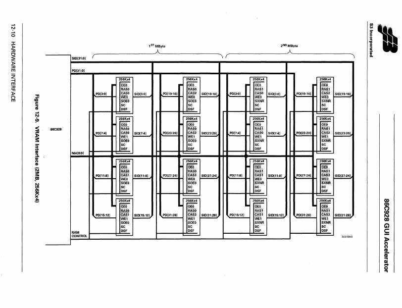
.... ~ 0
::I: l> 1ST MByte
:0
~ A
SI0[31:0] (
:0 m PO[31:0]
Z --I m :0 "TI
~ ~ OED OED RASO RASO
l> !! ("') cc m c: Cil
PO[3:0] CASO SI0[3:0] PO[19:16] CAS2 WED WED SOEO SOEO SC SC OSF OSF ...
1\1
!D ~ ~
~ Wo"" OED
< :0 l> 3:
86C928 RASO RASO
PO[7:4] CASO SI0[7:4] PO[23:20] CAS2 WE1 WE1 SOEO SOEO
S" ... SC SC OSF OSF
CD :::l.
MA[8:0] ~ ~
I\) n ~ ~ CD
r;3 3: $I'
Wo"" Wo"" RASO RASO
PO[11:8] CAS1 SI0[11:8] PO[27:24] CAS3 WED WED
1\1 (JI
SOEO SOEO SC SC
Q)
~ OSF OSF ~ -;e ~ ~
OED OED RA50 RASO
PO[15:12] CAS1 ~ PO[31:28] CAS3 WE1 WE1 SOEO SOEO SC SC
RAM OSF OSF
CONTROL ~ '---
2ND MByte
A "\ (
~ OED RAS1
510[19:16] PO[3:0] CASO SI0[3:0] PO[19:16] WED SXNR SC OSF
-~
OED RAS1
SI0[23:20] PO[7:4] CASO SI0[7:4] PO[23:20] WE1 SXNR SC OSF
-~
Wo'" RAS1
SI0[27:24] PO[11:8] CAS1 SI0[11:8] PO[27:24] WED SXNR SC OSF
-~
OED RAS1
SI0[31:28J PO[15:12J CAS1 SI0[15:12] PO[31:28J ---' WE1 ~
SXNR SC OSF
-
~ OED RAS1 CAS2 I SI0[19:16]1 WED SXNR SC OSF ~
~ OED RAS1 I
CAS2 n WE1 SXNR SC OSF ~
~
Wo""
~ RAS1 CAS3 WED SXNR SC OSF ~
~ OED RAS1 CAS3 ~ WE1 SXNR SC OSF
'--- 3001040
g: ;; " o -g ! ...
co
~ CO G')
S;;
l: (') CD
if ell ... o ...
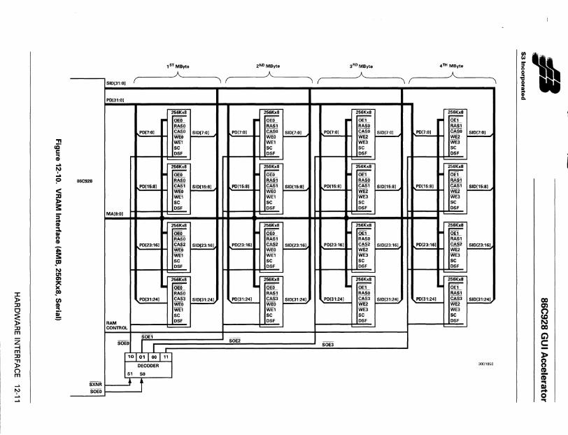
,ST MByte
A SID[31:0]
( '\ (
PD[31:0]
~ DEO RA50
PD[7:0] CA50 5ID[7:0] PD[7:0] WEO
." rE' WEI
SC e i
DSF ~ -~ - ~
DEO
? 86C928 RASO
< PD[15:8] CA51 SID[15:8] PD[15:8]
WEO :JJ WEI l> s: 5C
DSF
S" MA[8:0) .. CD
~ ~ OEO ...
CD
'i:
RA50 PD[23:16] CAS2 510(23:16] PD[23:16]
WEO
s: WE'
,!XI SC D5F
N U1 0'1
~ ~
ijfo"" ::c S1J RA50
l> :c
(f> CD
PD[3':24) CAS3 ~ PD[31:24] WEO
CJ
~ .. ~
WE. 5C
RAM D5F
:c CONTROL ~
m SOE1
Z -I m
50EO I 50E2
I :c -n l> ("') m
, '0101 I 00 I 11 I
Is. DECODER
I SO
-~
5XNR ---1 t SOEO
2 ND MByte 3 RD MByte
A '\ (
A ,.. ....
~ ~ DEO DEI RA51 RASO CASO 5ID[7:0] PD[7:0] CA50 WEO WE2 WEI WE3 SC SC D5F DSF ~ ~
~ ~ DEO DEI RASI RASO CAS1 5ID[15:8] PD[15:8] CAS1 WEO WE2 WEI WE3 SC SC DSF DSF
~
~ ~
~ ~ RAS1 RASO CAS2 5ID[23:16] PD[23:16) CAS2 WEO WE2 WEI WE3 5C 5C D5F D5F
~ ~ OEO OEI RAS1 RASO
~~~3 1 5ID[3' :24], PD[3':24) CA53 WE2
WEI WE3 5C 5C D5F DSF ~
50E3
4 TH MByte
A ... "
'\ (
~ DEI RAS1
510[7:0] PD[7:0] CA50 WE2 WE3 SC D5F ~
~ DEI RAS1
SID[15:8] PD[15:8] CAS1 WE2 WE3 SC DSF ~
~ OEI RAS1
510[23:16] PDI23:16] CAS2 WE2 WE3 5C DSF ~
~ OE. RA51
1 SID[3':24], PD[31:24] CAS3 WE2 WE3 5C DSF ~
1 5ID[7:0] ,
15ID[15:8] ,
1 5ID[23:16),
1 5ID[31:24),
3001050
I'lL ! --...
00
~ N 00 G') C
~ CD CD ... a o ...
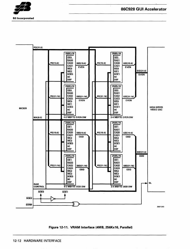
86C928 GUI Accelerator
53 Incorporated
P0131:01
2~ ""2s6i<ii'i'6 =-OEO ~ RASO RASl
PO[15:01 CASO 510[15:01 PO[15:01 CASO 510[15:01 CASl
EVEN CASl
EVEN WEO WEO WE2 WEl 510[31:01
SOEO SOEl EVEN SC SC OSF OSF
=-2~ ~ ~ OEO RASO RASl
PO[31:161 CAS2 510[31:161 PO[31:161 CAS2 510[31:161 CAS3 CAS3 WEO EVEN WEO EVEN
WEl WEl
86C928 SOEO SOEl HIGH SPEEO SC SC VIOEOOAC OSF OSF
MA[8:01 0-2 MBYTE EVEN OW 3-4'M'BYi'E EVEN OW
256Kx16 ""25iiKx'i"6 =- =-OEl OEl RASO RASl
PO[15:01 CASO 510[15:01 PO[15:01 CASO 510[15:01 CASl
000 CASl
000 WE2 WE2 WE3 WE3 SOEO SOEl SC sc OSF OSF
- 510[31:01
256Kx16 ""2s6i<ii'i'6 000 ........... =-OEl OEl RASO RASl
PO[31:161 CAS2 510[31:161 PO[31:161 CAS2 510[31:161 CAS3
000 CAS3
000 WE2 WE2 WE3 WE3 SOEO SOEl SC sc OSF OSF r+ SL
RAM ffiBvTE 000 OW CONTROL 3-4 MBYTE 000 OW
SOEO jEl
SOEO t I V
SXNR II 3001060
Figure 12-11. VRAM Interface (4MB, 256Kx16, Parallel!
12-12 HARDWARE INTERFACE
fl· S3 Incorporated
Table 12-4. Dot Clock Select Values
3C2H, Bits [3:2] PA[3:0]
00 0000
01 0001
10 0010
11 CR42, Bits [3:0]
The coding for these signals in this case is as shown in Table 12-5.
Table 12-5. Dot Clock Select Coding
PA[3:0] Freq Mode (HEX) (MHz)
0 25.175 VGAO
1 28.322 VGA1
2 40.000 VESA 800x600 @60Hz
3 Reserved
4 50.000 VESA 800x600 @72Hz 640x480x16bpp @ 60Hz
5 77.000 1 024x768 @72Hz
6 36.000 VESA 800x600 @56Hz
7 44.889 1 024x768 @43Hz - I
8 Reserved
9 Reserved A 80.000 1280x1 024 @46Hz - I
B 31.500 VESA 640x480 @72Hz
C 110.000 1280x1 024 @60Hz
D 65.000 1 024x768 @60Hz
E 75.000 1 024x768 @70Hz 640x480x24bpp @ 60 Hz
F Reserved
Note: In Table 12-5, I means interlaced. This table is an example, as the frequencies are dependent upon the clock synthesizer capabilites.See the 53-Compatible Clock Generators tech note.
If bit 5 ofthe Clocking Mode register (3C5H, Index 01 H) is reset to 0, the screen display is turned on and STWR will be asserted once during every VSYNC interval as shown in Figure 12-13.
Having STWR asserted when the screen display is turned off is desirable because the clock chip on Iy re-syncs its outputs when the latched
86C928 GUI Accelerator
PA[3:0] inputs have changed since the previous falling edge of STWR. This prevents screen jitter when the 86C928 selects the same clock value multiple times.
12.7 GENERAL I/O PORT
The 86C928 provides an 8-bit General Input Port and a 4-bit General Output Port. The block diagram showing how these are implemented is shown in Figure 12-14.
Bit 2 ofthe Extended DAC Control register (3?5H, Index 55H) and bit 1 ofthe System Configuration register (3?5H, Index 40H) are set to 1 to enable the General Input Port read function. The data to be read is held in an external buffer and is read via port 3C8H (the same as the DAC Write Index off-chip register). When STRD is asserted, this data is driven onto the SD[7:0]linestothe ISNLocal bus. The STRD assertion timing is identical to the DACRD timing.
The General Output Port register (3?5H, Index 5CH) bits [7:4] can be set to any value by a CPU write. The programmed values appear on PA[7:4] and are latched into the GOP external buffer whenever STWR is asserted. See Section 12.6 for a description of when STWR is asserted.
12.8 NTSC/PAL VIDEO INTERFACE
The 86C928 provides the capability to synchronize its video output with a remote video (NTSC, PAL or other PC video) signal. The first step is to enter remote mode by setting bit 0 ofthe External Sync Cont 1 (3?5H, Index 56H) register to 1. The VSYNC pin becomes an input to the 86C928. The falling edge of VSYNC resets the HN counter to 0, corresponding to the top left corner of the display. The External Sync Cont 2 (3?5H, Index 57) is then programmed to match the falling edge of the VSYNC signal with the HN counter reset. This technique works well with a remote video signal using the same dot clock oscillator as the 86C928.
HARDWARE INTERFACE 12-13
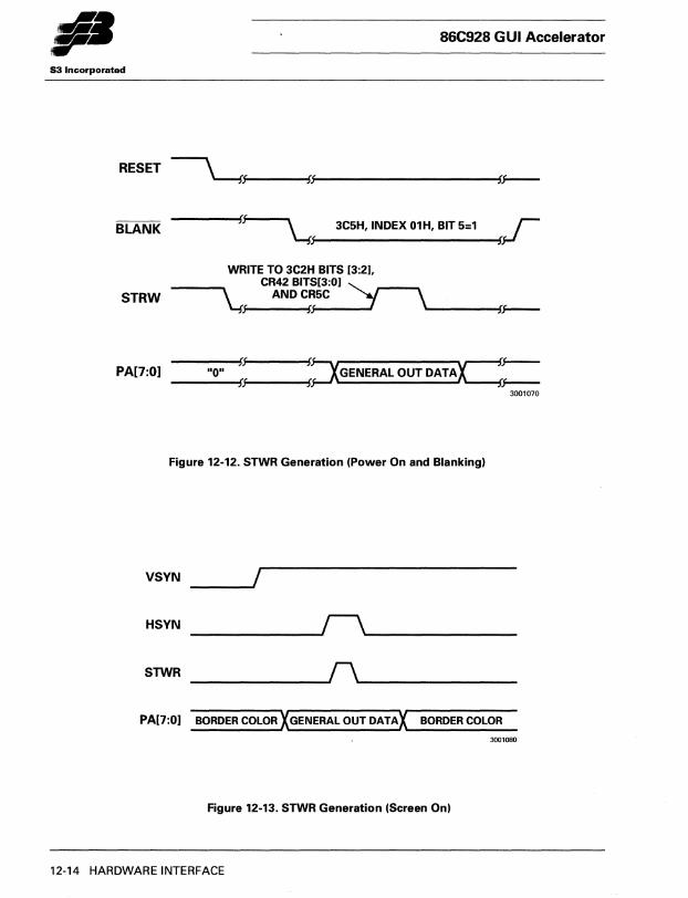
II· 86C928 GUI Accelerator
S3 Incorporated
RESET ~ ~jr------~lir-------------------~fj----
BLANK :~ 3C5H, INDEX 01H, BIT 5=1 Yj fF
WRITE TO 3C2H BITS [3:2],
STRW C~~~~~~~O] ": r--\
\Y: n ~ \~'----~fj----
PA[7:0] _____ .. O_'_'~~li~------..,~:=xGENERALOUTDATA~ 3001070
Figure 12-12. STWR Generation (Power On and Blanking)
VSYN ____ .....J/
HSYN __________ .....Jr--\~ __________ _
STWR __________ .....Jf\~ __________ __
PA[7:0] BORDER COLOR X GENERAL OUT DATAX BORDER COLOR
3001000
Figure 12-13. STWR Generation (Screen On)
12-14 HARDWARE INTERFACE
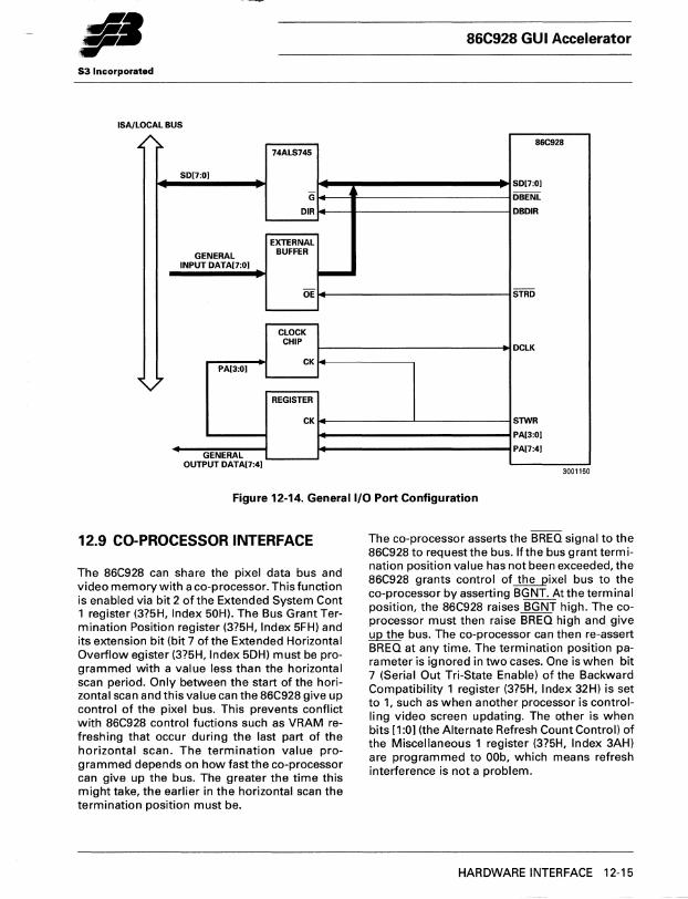
II· 86C928 GUI Accelerator
S3 Incorporated
ISA/LOCAL BUS
.I. ~ 86C928 74ALS745
SO[7:0] SO[7:0]
G OBENL
OIR OBOIR
EXTERNAL
GENERAL BUFFER
INPUT OATA[7:0] ---OE STRO
CLOCK CHIP
OCLK
CK PA[3:0]
... 7'
REGISTER
CK STWR
PA[3:0]
GENERAL PA[7:4]
OUTPUT OATA[7:4] 3001150
Figure 12-14. General 1/0 Port Configuration
12.9 CO-PROCESSOR INTERFACE
The 86C928 can share the pixel data bus and video memory with a co-processor. This function is enabled via bit 2 ofthe Extended System Cont 1 register (3?5H, Index 50H). The Bus Grant Termination Position register (3?5H, Index 5FH) and its extension bit (bit 7 of the Extended Horizontal Overflow egister (3?5H, Index 5DH) must be programmed with a value less than the horizontal scan period. Only between the start of the horizontal scan and this value can the 86C928 give up control of the pixel bus. This prevents conflict with 86C928 control fuctions such as VRAM refreshing that occur during the last part of the horizontal scan. The termination value programmed depends on how fast the co-processor can give up the bus. The greater the time this might take, the earlier in the horizontal scan the termination position must be.
The co-processor asserts the BREQ signal to the 86C928 to request the bus. If the bus grant term ination position value has not been exceeded, the 86C928 grants control of~ixel bus to the co-processor by asserting BGNT. At the terminal position, the 86C928 raises BGNT high. The coprocessor must then raise BREO high and give up the bus. The co-processor can then re-assert BREO at any time. The termination position parameter is ignored in two cases. One is when bit 7 (Serial Out Tri-State Enable) of the Backward Compatibility 1 register (3?5H, Index 32H) is set to 1, such as when another processor is controlling video screen updating. The other is when bits [1:0] (the Alternate Refresh Count Control) of the Miscellaneous 1 register (3?5H, Index 3AH) are programmed to OOb, which means refresh interference is not a problem.
HARDWARE INTERFACE 12-15
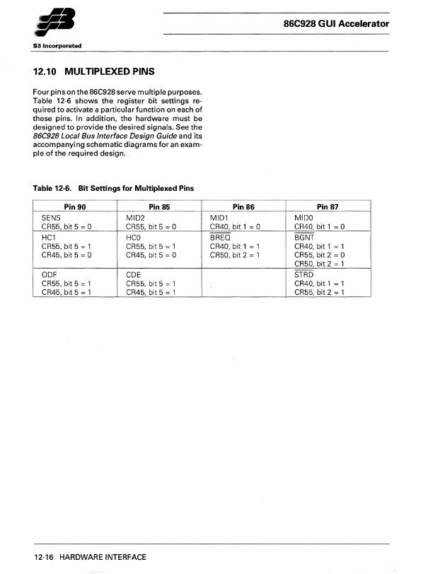
.... r S3 Incorporated
12.10 MULTIPLEXED PINS
Four pins on the 86C928 serve multiple purposes. Table 12-6 shows the register bit settings required to activate a particular function on each of these pins. In addition, the hardware must be designed to provide the desired signals. See the 86C928 Local Bus Interface Design Guide and its accompanying schematic diagrams for an example ofthe required design.
Table 12-6. Bit Settings for Multiplexed Pins
Pin 90 Pin 85
SENS MID2 CR55, bit 5 = ° CR55, bit 5 = ° HC1 HCO CR55, bit 5 = 1 CR55, bit 5 = 1 CR45, bit 5 = ° CR45, bit 5 = ° ODF CDE CR55, bit 5 = 1 CR55, bit 5 = 1 CR45, bit 5 = 1 CR45, bit 5 = 1
12-16 HARDWARE INTERFACE
86C928 GUI Accelerator
Pin 86 Pin 87
MID1 MIDO CR40, bit 1 = ° CR40, bit 1 = ° BREQ BGNT CR40, bit 1 = 1 CR40, bit 1 = 1 CR50, bit 2 = 1 CR55, bit 2 = °
CR50, bit 2 = 1
STRD CR40, bit 1 = 1 CR55, bit 2 = 1
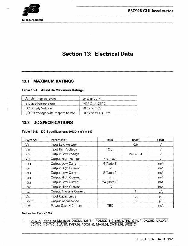
II· 86C928 GUI Accelerator
53 Incorporated
Section 13: Electrical Data
13.1 MAXIMUM RATINGS
Table 13-1. Absolute Maximum Ratings
Ambient temperature 0° C to 70° C
Storage temperature -40° C to 125° C
DC Supply Voltage -0.5V to 7.0V
I/O Pin Voltage with respect to VSS -0.5V to VDD+0.5V
13.2 DC SPECIFICATIONS
Table 13-2. DC Specifications (VDD = 5V ± 5%)
Symbol Parameter Min Max Unit
VIL Input Low Voltage 0.8 V
VIH Input High Voltage 2.0 V
VOL Output Low Voltage Vss + 0.4 V
VOH Output High Voltage VDD - OA V
lOll Output Low Current 4 (Note 1) mA
IOHl Output High Current -2 mA
IOL2 Output Low Current 8 (Note 2) mA
IOH2 Output HiQh Current -4 mA
IOL3 Output Low Current 24 (Note 3) mA
IOH3 Output High Current -12 mA
loz Output Tri-state Current 1 /LA
CIN Input Capacitance 5 pF
COUT Output Capacitance 5 pF
Icc Power Supply Current TBD mA
Notes for Table 13-2
1. lOll, IOHl for pins SD[15:0], DBENL, SINTR, ROMCS, HC[1:0]' STRD, STWR, DACRD, DACWR, VSYNC, HSYNC, BLANK, PA[7:0], PD[31:0], MA[8:0], CAS[3:0], WE[3:0]
ELECTRICAL DATA 13-1
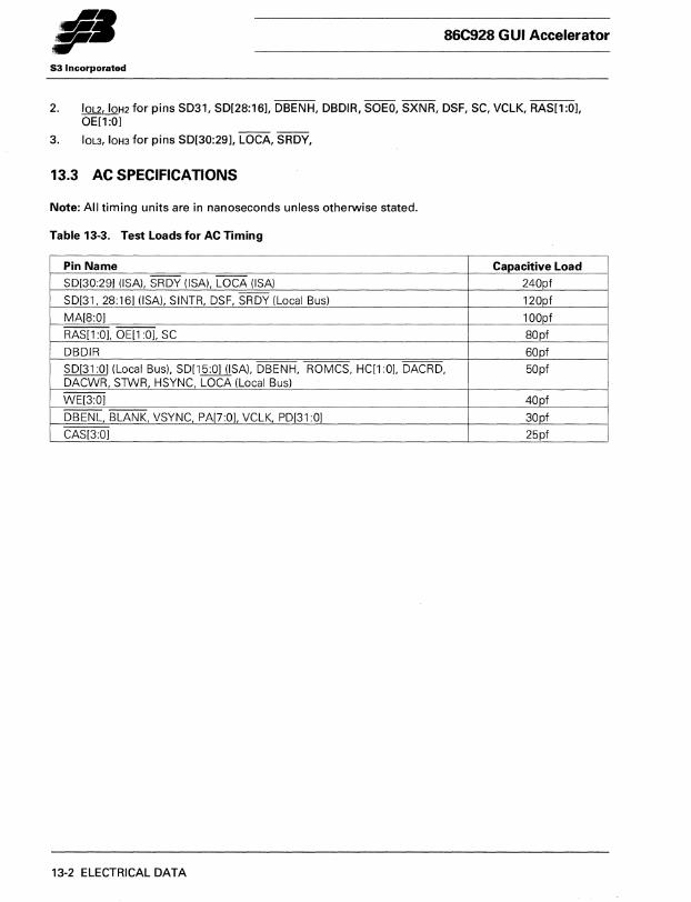
86C928 GUI Accelerator
S3 Incorporated
2. IOL2, IOH2 for pins S031, SO[28:16), OBENH, OBOIR, SOEO, SXNR, OSF, SC, VCLK, RAS[1:0], OE[1:0]
3. IOL3, IOH3 for pins SO[30:29), LOCA, SROY,
13.3 AC SPECIFICATIONS
Note: All timing units are in nanoseconds unless otherwise stated.
Table 13·3. Test Loads for AC Timing
Pin Name Capacitive Load SD[30:29] (ISA). SRDY (ISA). LOCA (ISA) 240pf
SO[31, 28:16] (ISA), SINTR, DSF, SRDY (Local Bus) 120pf
MA[8:0] 100pf
RAS[l :01. OE[l :01. SC 80pf
DBDIR 60pf
SD[31:0] (Local Bus). SO[15:0] (lSA). DBENH, ROMCS, HC[l :01. DACRD, 50pf DACWR, STWR, HSYNC, LOCA (Local Bus)
WE[3:0] 40pf
OBENL, BLANK, VSYNC, PA[7:01, VCLK, PD[31 :0] 30pf
CAS[3:0] 25pf
13-2 ELECTRICAL OATA
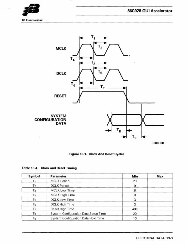
S3 Incorporated
MCLK
DCLK
RESET
SYSTEM CONFIGURATION
DATA
Figure 13-1. Clock And Reset Cycles
Table 13-4. Clock and Reset Timing
Symbol Parameter
T1 MCLK Period
T2 DCLK Period
T3 MCLK Low Time
T4 MCLK High Time
T5 DCLK Low Time
T6 DCLK High Time
T7 Reset High Time
T8 System Configuration Data Setup Time
T9 System Configuration Data Hold Time
86C928 GUI Accelerator
3000900
Min Max
20 9
8 8
3
3
400 20 10
ELECTRICAL DATA 13-3
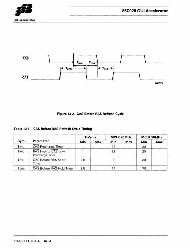
86C928 GUI Accelerator
53 Incorporated
RAS
3000970
Figure 13-2. CAS Before RAS Refresh Cycle
Table 13-5. CAS Before RAS Refresh Cycle Timing
T-Value MCLK45MHz MCLK50MHz Sym. Parameter Min Max Min Max Min Max
TCPN CAS Precharge Time 1 22 20 TRPc RAS High to CAS Low 1 22 20
Precharge Time
TcsR CAS Before RAS Setup 1.5 33 30 Time
TCHR CAS Before RAS Hold Time 3.5 77 70
13-4 ELECTRICAL DATA
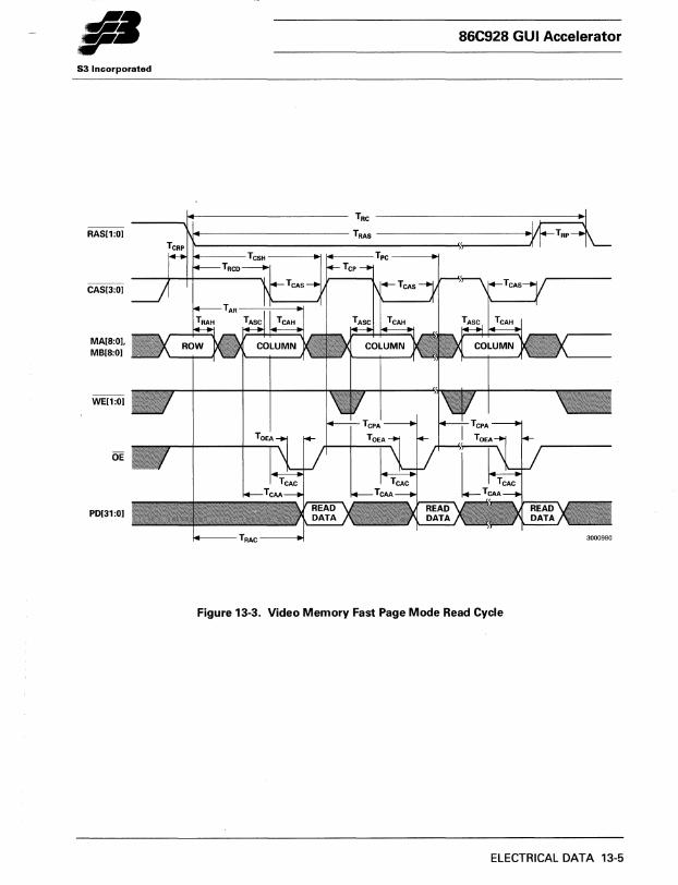
•• r 86C928 GUI Accelerator
S3 Incorporated
----Ji---------- TRC
RAS[1:01
CAS[3:01
MA[8:01. MB[8:01
WE[1:01
OE
PD[31:01
~~-------------TRAS -----------~,f~-
Figure 13-3. Video Memory Fast Page Mode Read Cycle
ELECTRICAL DATA 13-5
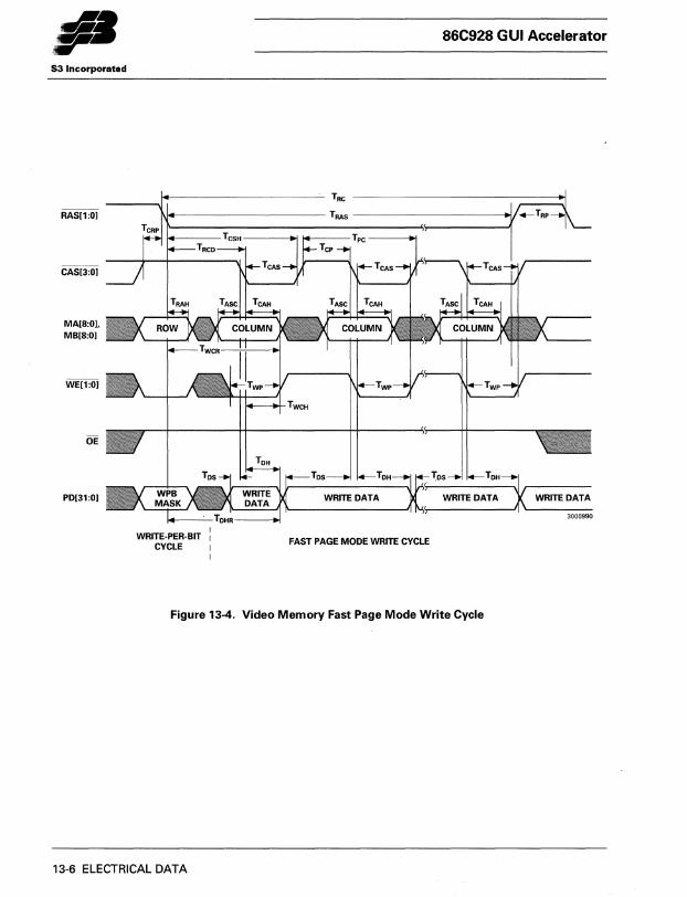
53 Incorporated
RAS[1:0]
CAS[3:0]
MA[8:01. MB[8:0]
WE[1:0]
OE
PD[31:0]
WRITE-PER-BIT CYCLE
FAST PAGE MODE WRITE CYCLE
86C928 GUI Accelerator
Figure 13-4_ Video Memory Fast Page Mode Write Cycle
13-6 ELECTRICAL DATA
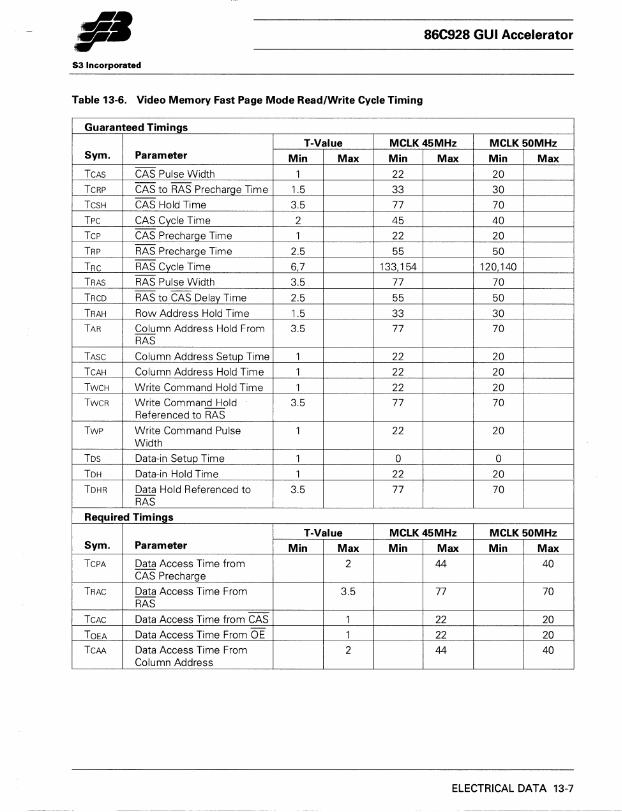
• .6Ja ,.. S3 Incorporated
86C928 GUI Accelerator
Table 13-6. Video Memory Fast Page Mode Read/Write Cycle Timing
Guaranteed Timings
T-Value MCLK45MHz MCLK50MHz Sym. Parameter Min Max Min Max Min Max TCAS CAS Pulse Width 1 22 20 TCRP CAS to RAS Precharge Time 1.5 33 30 TcsH CAS Hold Time 3.5 77 70 Tpc CAS Cycle Time 2 45 40 Tcp CAS Precharge Time 1 22 20 TRP RAS Precharge Time 2.5 55 50 TRC RAS Cycle Time 6,7 133,154 120,140 TRAS RAS Pulse Width 3.5 77 70 TRCD RAS to CAS Delay Time 2.5 55 50 TRAH Row Address Hold Time 1.5 33 30 TAR Column Address Hold From 3.5 77 70
RAS
TASC Column Address Setup Time 1 22 20 TCAH Column Address Hold Time 1 22 20 TWCH Write Command Hold Time 1 22 20 TWCR Write Command Hold 3.5 77 70
Referenced to RAS
Twp Write Command Pulse 1 22 20 Width
TDS Data-in Setup Time 1 0 0 TDH Data-in Hold Time 1 22 20 TDHR Data Hold Referenced to 3.5 77 70
RAS
Required Timings
T-Value MCLK45MHz MCLK50MHz Sym. Parameter Min Max Min Max Min Max TCPA Data Access Time from 2 44 40
CAS Precharge
TRAC Data Access Time From 3.5 77 70 RAS
TCAC Data Access Time from CAS 1 22 20 TOEA Data Access Time From OE 1 22 20 TCM Data Access Time From 2 44 40
Column Address
ELECTRICAL DATA 13-7
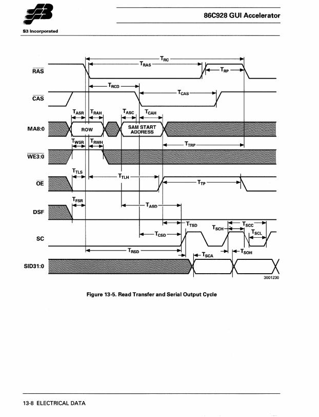
86C928 GUI Accelerator
53 Incorporated
CAS
MA8:0
WE3:0
OE
DSF
SC
SID31:0
~----------~=----TRc-----------------;~ --------~I ~------------TRAs------------~ ~--------~
Figure 13-5. Read Transfer and Serial Output Cycle
13-8 ELECTRICAL DATA
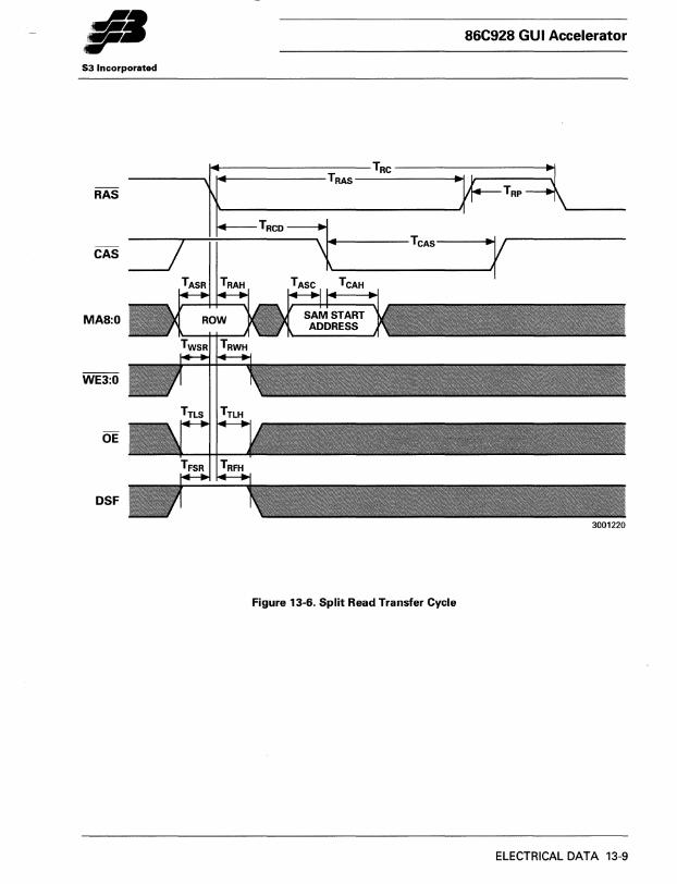
86C928 GUI Accelerator
53 Incorporated
RAS
CAS
MA8:0
WE3:0
OE
DSF
~-------------------TRC------------------~~ ----.....,.1 ~-----------T RAS --------------+{ 1,...---------... 1
Figure 13-6. Split Read Transfer Cycle
3001220
ELECTRICAL DATA 13-9
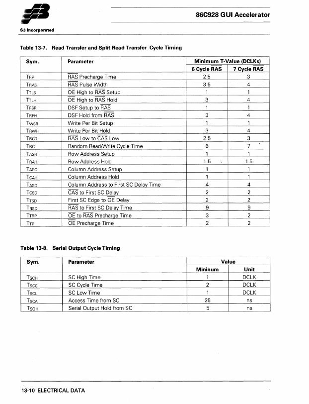
86C928 GUI Accelerator
53 Incorporated
Table 13-7. Read Transfer and Split Read Transfer Cycle Timing
Sym. Parameter Minimum T-Value (DCLKs)
6 Cycle RAS 7 Cvcle RAS
TRP RAS Precharge Time 2.5 3
TRAS RAS Pulse Width 3.5 4
TTLS OE High to RAS Setup 1 1
TTLH OE High to RAS Hold 3 4
TFSR DSF Setup to RAS 1 1
TRFH DSF Hold from RAS 3 4
TWSR Write Per Bit Setup 1 1
TRWH Write Per Bit Hold 3 4
TRCD RAS Low to CAS Low 2.5 3
TRC Random ReadIWrite Cycle Time 6 7
TASR Row Address Setup 1 1
TRAH Row Address Hold 1.5 1.5
TASC Column Address Setup 1 1
TCAH Column Address Hold 1 1
TASD Column Address to First SC Delay Time 4 4
TCSD CAS to First SC Delay 2 2
TTSD First SC Edge to OE Delay 2 2
TRSD RAS to First SC Delay Time 9 9
TTRP OE to RAS Precharge Time 3 2
TTP OE Precharge Time 2 2
Table 13-8. Serial Output Cycle Timing
Sym. Parameter Value
Mininum Unit
TSCH SC High Time 1 DCLK
Tscc SC Cycle Time 2 DCLK
TSCL SC Low Time 1 DCLK
TSCA Access Time from SC 25 ns
TSOH Serial Output Hold from SC 5 ns
13-10 ELECTRICAL DATA
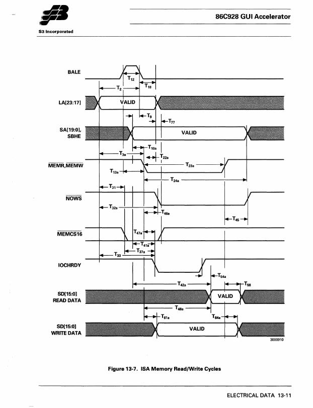
... r S3 Incorporated
BALE
LA[23:17]
SA[19:0], SBHE
NOWS
MEMCS16
IOCHROV
SO[15:0] REAOOATA
SO[15:0] WRITEOATA
86C928 GUI Accelerator
3000910
Figure 13-7. ISA Memory Read/Write Cycles
ELECTRICAL DATA 13-11
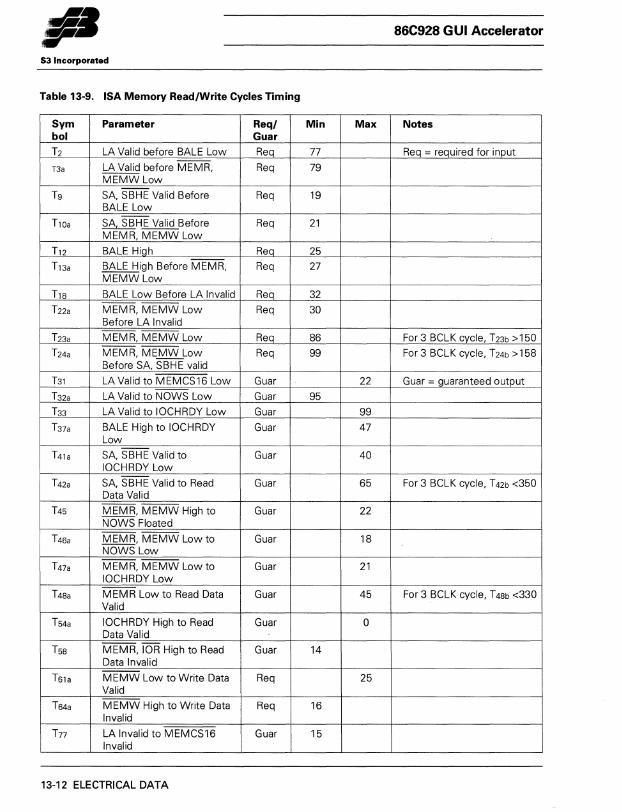
86C928 GUI Accelerator
53 Incorporated
Table 13-9. ISA Memory Read/Write Cycles Timing
Sym Parameter Req/ Min Max Notes bol Guar T2 LA Valid before BALE Low Req 77 Req = required for input
T3a LA Valid before MEMR, Req 79 MEMWLow
Tg SA, SBHE Valid Before Req 19 BALE Low
T10a SA, SBHE Valid Before Req 21 MEMR, MEMW Low
T12 BALE High Req 25
T13a BALE High Before MEMR, Req 27 MEMW Low
T18 BALE Low Before LA Invalid Req 32
T22a MEMR, MEMW Low Req 30 Before LA Invalid
--
T23a MEMR, MEMW Low Req 86 For 3 BCLK cycle, T 23b > 150
h4a MEMR, MEMW Low Req 99 For 3 BCLK cycle, T24b >158 Before SA, SBHE valid
T31 LA Valid to MEMCS16 Low Guar 22 Guar = guaranteed output
T32a LA Valid to NOWS Low Guar 95 --
T33 LA Valid to IOCHRDY Low Guar 99
T37a BALE High to IOCHRDY Guar 47 Low
T41a SA, SBHE Valid to Guar 40 IOCHRDY Low
T42a SA, SBHE Valid to Read Guar 65 For 3 BCLK cycle, T42b <350 Data Valid
T45 MEMR, MEMW High to Guar 22 NOWS Floated
T46a MEMR, MEMW Low to Guar 18 NOWS Low
T47a MEMR, MEMW Low to Guar 21 IOCHRDY Low
T48a MEMR Low to Read Data Guar 45 For 3 BCLK cycle, T 48b <330 Valid
T54a IOCHRDY High to Read Guar 0 Data Valid
T58 MEMR, lOR High to Read Guar 14 Data Invalid
T61a MEMW Low to Write Data Req 25 Valid
T64a MEMW High to Write Data Req 16 Invalid
T77 LA Invalid to MEMCS16 Guar 15 Invalid
13-12 ELECTRICAL DATA
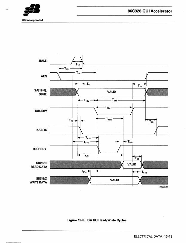
S3 Incorporated
BALE
AEN
5A[19:0], 5BHE
10R,IOW
IOC516
10CHROY
50[15:0] REAOOATA
50[15:0] WRITEOATA
86C928 GUI Accelerator
---~~------------~--- T74 -----1~
VAllO
-~---T240 ------~
VAllO
3000920
Figure 13-8. ISA 1/0 Read/Write Cycles
ELECTRICAL DATA 13-13
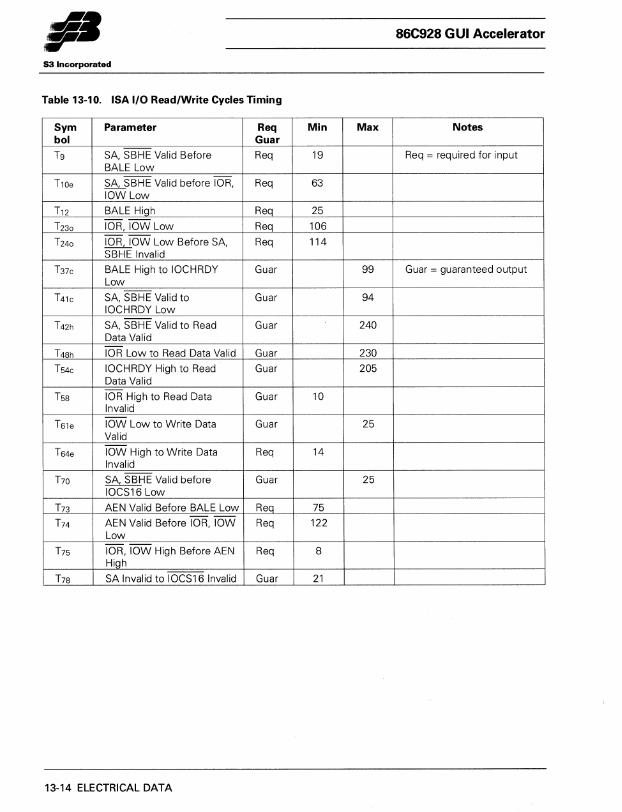
-~. r S3 Incorporated
Table 13-10. ISA I/O Read/Write Cycles Timing
Sym Parameter Req bol Guar Tg SA, SBHE Valid Before Req
BALE Low
T10e SA, SBHE Valid before lOR, Req lOW Low
T12 BALE High Req
T230 10R,IOWLow Req
T240 lOR, lOW Low Before SA, Req SBHE Invalid
T37c BALE High to 10CHRDY Guar Low
T4lc SA, SBHE Valid to Guar 10CHRDY Low
T42h SA, SBHE Valid to Read Guar Data Valid
T48h lOR Low to Read Data Valid Guar
T54c 10CHRDY High to Read Guar Data Valid
T58 lOR High to Read Data Guar Invalid
T6le lOW Low to Write Data Guar Valid
T64e lOW High to Write Data Req Invalid
T70 SA, SBHE Valid before Guar IOCS16 Low
T73 AEN Valid Before BALE Low Req
T74 AEN Valid Before lOR, lOW Req Low
T75 lOR, lOW High Before AEN Req High
T78 SA Invalid to IOCS16 Invalid Guar
13-14 ELECTRICAL DATA
86C928 GUI Accelerator
Min Max Notes
19 Req = required for input
63
25
106
114
99 Guar = guaranteed output
94
240
230
205
10
25
14
25
75
122
8
21
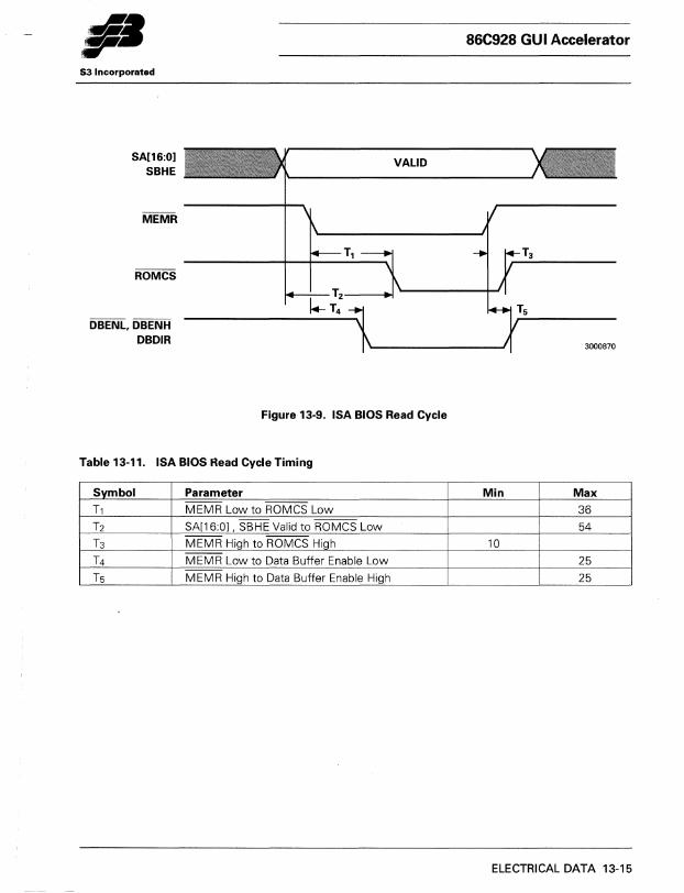
53 Incorporated
SA[16:0] SBHE
MEMR
ROMCS
DBENL, DBENH DBDIR
VALID
Figure 13·9. ISA BIOS Read Cycle
Table 13·11. ISA BIOS Read Cycle Timing
Svmbol Parameter
T1 MEMR Low to ROMCS Low
T2 SA[16:0[ , SBHE Valid to ROMCS Low
T3 MEMR High to ROMCS High
T4 MEMR Low to Data Buffer Enable Low
T5 MEMR High to Data Buffer Enable High
86C928 GUI Accelerator
3000870
Min Max
36
54
10
25
25
ELECTRICAL DATA 13·15
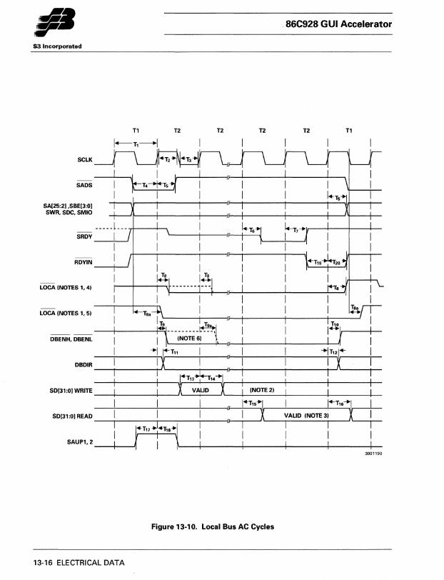
•• r . 86C928 GUI Accelerator
S3 Incorporated
T1 T2 T2 T2 T2 T1
I--T,-I
SCLK
SADS
SA[25:2] ,SBE[3:0] SWR, SOC, SMIO
SRDY
RDYIN
LOCA (NOTES 1, 4) 1
1 1
LOCA (NOTES 1, 5) 1 ~n-
I" '"I 1 T,o 1
---- I-I 1
DBENH,DBENL I-t --(-~~~~ :--!, , 1 :5
-'1 I+T" 1 -'IT12I+ 1
DBDIR 1 ~ 1 : 1 ~ 1
1 I.T,3J.-T'4+1 1 1
SD[31:0] WRITE I ~ V~LlD ~ (NOTE 2) I I 1 1
SD[31:0] READ 1 1
r't'''1 1
1 SAUP1,2
1 3001190
Figure 13-10. Local Bus AC Cycles
13-16 ELECTRICAL DATA
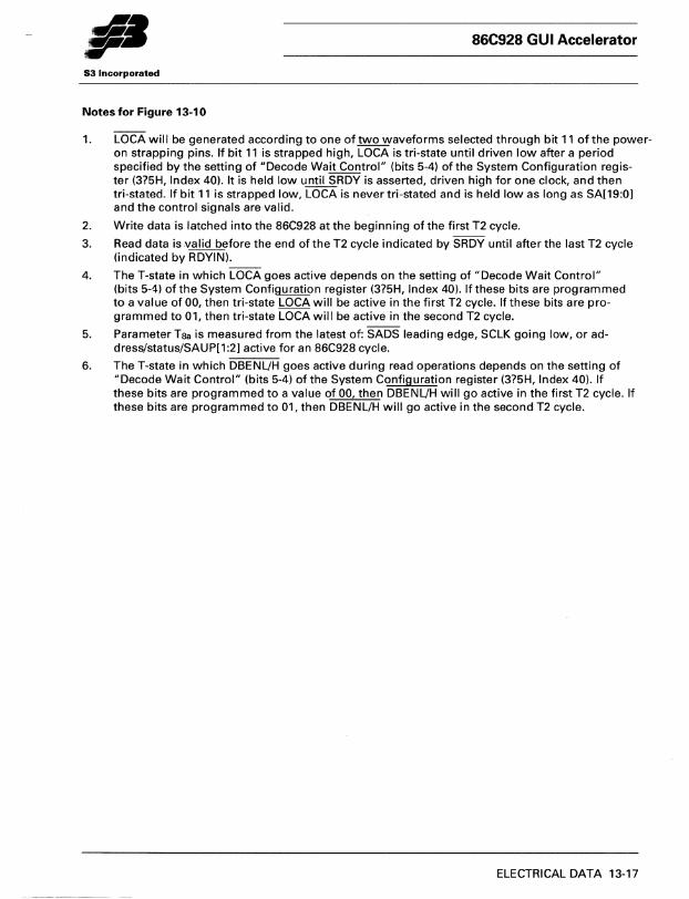
86C928 GUI Accelerator
S3 Incorporated
Notes for Figure 13-10
1. LOCA will be generated according to one of two waveforms selected through bit 11 of the poweron strapping pins. If bit 11 is strapped high, LOCA is tri-state until driven low after a period specified by the setting of "Decode Wait Control" (bits 5-4) of the System Configuration regis-ter (3?5H, Index 40). It is held low until SRDY is asserted, driven high for one clock, and then tri-stated. If bit 11 is strapped low, LOCA is never tri-stated and is held low as long as SA[19:0] and the control signals are valid.
2. Write data is latched into the 86C928 at the beginning of the first T2 cycle.
3. Read data is ,valid before the end of the T2 cycle indicated by SRDY until after the last T2 cycle (indicated by RDYIN).
4. The T-state in which LOCA goes active depends on the setting of "Decode Wait Control" (bits 5-4) ofthe System Configuration register (3?5H, Index 40). Ifthese bits are programmed to a value of 00, then tri-state LOCA will be active in the first T2 cycle. If these bits are programmed to 01, then tri-state LOCA will be active in the second T2 cycle.
5. Parameter Taa is measured from the latest of: SADS leading edge, SCLK going low, or address/status/SAUP[1:2] active for an 86C928 cycle.
6. The T-state in which DBENL/H goes active during read operations depends on the setting of "Decode Wait Control" (bits 5-4) of the System Configuration register (3?5H, Index 40). If these bits are programmed to a value of 00, then DBENL/H will go active in the first T2 cycle. If these bits are programmed to 01, then DBENL/H will go active in the second T2 cycle.
ELECTRICAL DATA 13-17
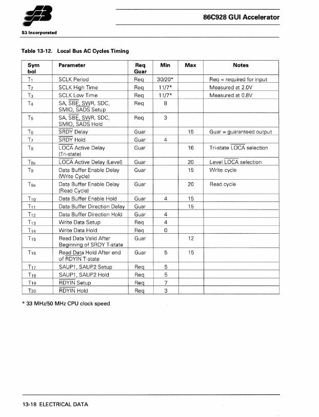
86C928 GUI Accelerator
53 Incorporated
Table 13-12. Local Bus AC Cycles Timing
Sym Parameter Req Min Max Notes bol Guar
T1 SCLK Period Req 30/20* Req = required for input
T2 SCLK HiQh Time Req 11/7* Measured at 2.OV
T3 SCLK Low Time Req 11/7* Measured at 0.8V
T4 SA, SBE, SWR, SDC, Req 8 SMIO, SADS Setup
T5 SA. SBE, SWR, SDC, Req 3 SMIO, SADS Hold
T6 SRDY Delay Guar 15 Guar = guaranteed output
T7 SRDY Hold Guar 4
T8 LOCA Active Delay Guar 16 Tri-state LOCA selection (Tri-state)
T8a LOCA Active Delay (Level) Guar 20 Level LOCA selection
T9 Data Buffer Enable Delay Guar 15 Write cycle (Write Cycle)
T9a Data Buffer Enable Delay Guar 20 Read cycle (Read Cycle)
TlO Data Buffer Enable Hold Guar 4 15
T11 Data Buffer Direction Delay Guar 15
T12 Data Buffer Direction Hold Guar 4
T13 Write Data Setup Req 4
T14 Write Data Hold Req 0
T15 Read Data Valid After Guar 12 Beginning of SRDY T-state
T16 Read Data Hold After end Guar 5 15 of RDYIN T-state
T17 SAUP1, SAUP2 Setup Req 5
T18 SAUP1, SAUP2 Hold Req 5
T19 RDYIN Setup Req 7
120 RDYIN Hold Req 3
* 33 MHz/50 MHz CPU clock speed
13-18 ELECTRICAL DATA
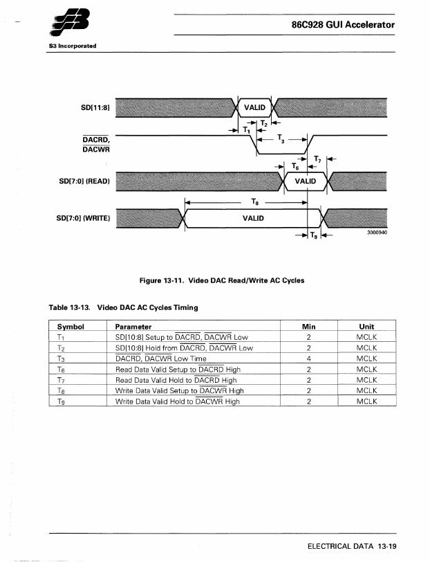
•• r 53 Incorporated
SO[11:8]
OACRO. OACWR
SO[7:0] (REAO)
SO[7:0] (WRITE)
86C928 GUI Accelerator
Figure 13-11. Video OAC Read/Write AC Cycles
Table 13-13. Video OAC AC Cycles Timing
Symbol Parameter Min Unit
T1 SD[1 0:8] Setup to DACRD, DACWR Low 2 MCLK
T2 SD[10:81 Hold from DACRD, DACWR Low 2 MCLK
T3 DACRD, DACWR Low Time 4 MCLK
T6 Read Data Valid Setup to DACRD High 2 MCLK
T7 Read Data Valid Hold to DACRD High 2 MCLK
T8 Write Data Valid Setup to DACWR High 2 MCLK
T9 Write Data Valid Hold to DACWR High 2 MCLK
ELECTRICAL DATA 13-19
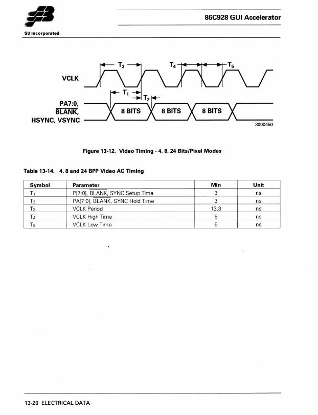
86C928 GUI Accelerator
S3 Incorporated
VCLK
PA7:0, BLANK,
HSVNC,VSVNC
rr T, T2r,: --""'\X S BITS X -S-B-IT-S---'X S BITS X'-___ _ 3000450
Figure 13-12. Video Timing - 4, 8, 24 Bits/Pixel Modes
Table 13-14. 4,8 and 24 BPP Video AC Timing
Symbol Parameter Min Unit
T1 P[7:01. BLANK, SYNC Setup Time 3 ns T2 PA[7:01. BLANK, SYNC Hold Time 3 ns T3 VCLK Period 13.3 ns T4 VCLK High Time 5 ns T5 VCLK Low Time 5 ns
13-20 ELECTRICAL DATA
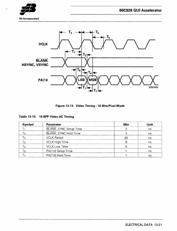
S3 Incorporated
VCLK
BLANK HSVNC,VSVNC
PA7:0
86C928 GUI Accelerator
Figure 13·13. Video Timing· 16 Bits/Pixel Mode
Table 13·15. 16 BPP Video AC Timing
Symbol Parameter Min Unit T1 BLANK, SYNC Setup Time 3 ns T2 BLANK, SYNC Hold Time 3 ns T3 VCLK Period 20 ns T4 VCLK High Time 8 ns T5 VCLK Low Time 8 ns T6 PA[7:0[ Setup Time 1 ns T7 PA[7:0] Hold Time 7 ns
ELECTRICAL DATA 13·21
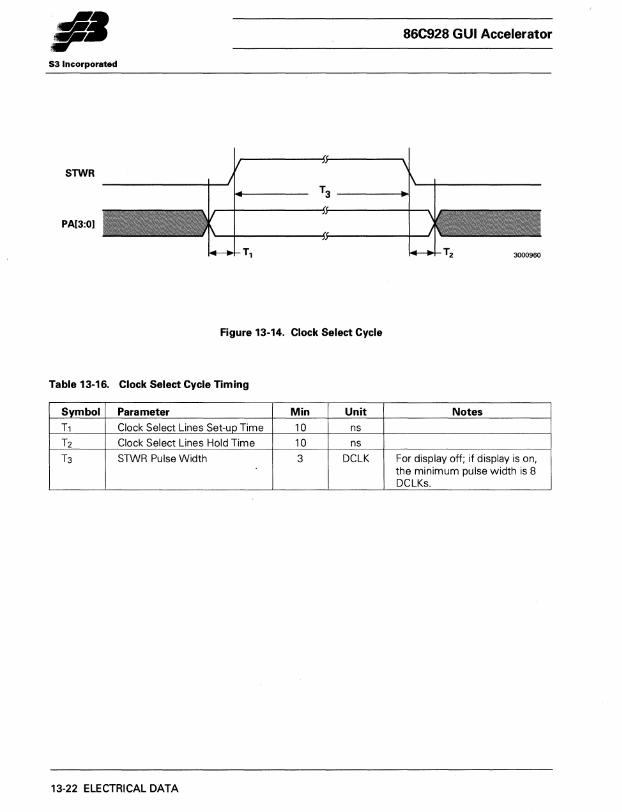
- ... r S3 Incorporated
STWR
PA[3:0]
T,
Figure 13-14. Clock Select Cycle
Table 13-16. Clock Select Cycle Timing
Symbol Parameter Min Unit
T1 Clock Select Lines Set-~ Time 10 ns
T2 Clock Select Lines Hold Time 10 ns
T3 STWR Pulse Width 3 DCLK
13-22 ELECTRICAL DATA
86C928 GUI Accelerator
Notes
For display off; if display is on, the minimum pulse width is 8 DCLKs.
86C928 GUI Accelerator
S3 Incorporated
Section 14: Mechanical Data
14.1 MECHANICAL DIMENSIONS
The mechanical dimensions for the 86C928 are given in Figure14-1.
MECHANICAL DATA 14-1
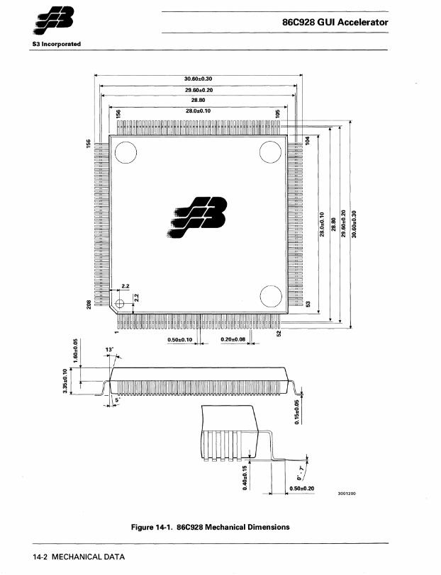
II· S3 Incorporated
~ .,; +I II)
'" "'"---~
14-2 MECHANICAL DATA
86C928 GUI Accelerator
30.60~0.30
29.60",0.20
3001200
Figure 14-1. 86C928 Mechanical Dimensions
86C928 GUI Accelerator
53 Incorporated
Appendix A: Register Reference
This Appendix contains tables listing all the registers in each of categories corresponding to Sections 4-10 ofthis data book.
• CGA-Compatible
• MDA- and HGC- Compatible
• VGA
• S3VGA
• System Control
• System Extension
• Enhanced Commands
Within each table, registers are listed in order of increasing addresses/indices. Name, mnemonic, address, read/write status and page number of detailed description are provided for each register. All addresses and indices are hexadecimal values.
REGISTER REFERENCE A-1
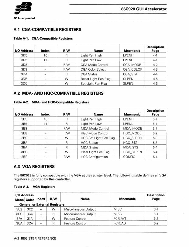
86C928 G UI Accelerator
53 Incorporated
A.1 CGA-COMPATIBLE REGISTERS
Table A-1. CGA-Compatible Registers
Description I/O Address Index R/W Name Mnemonic Page
3D5 10 R LiQht Pen HiQh LPENH 4-1
305 11 R Light Pen Low LPENL 4-1
3D8 - R/W CGA Mode Control CGA MODE 4-2
3D9 - R/W CGA Color Select CGA COLOR 4-3
3DA - R CGA Status CGA STAT 4-4
3DB - W Reset Light Pen Flag CLPEN 4-5
3DC - W Set Light Pen Flag SLPEN 4-5
A.2 MDA- AND HGC-COMPATIBLE REGISTERS
Table A-2. MDA- and HGC-Compatible Registers
Description I/O Address Index R/W Name Mnemonic Page
3B5 10 R Light Pen High LPENH 5-1 3B5 11 R Light Pen Low LPENL 5-1
3B8 - R/W MDA-Mode Control MDA MODE 5-1
3B8 - R/W HGC-Mode Control HGC MODE 5-2
3B9 - W HGC-Set Light Pen Flag HGC SLPEN 5-3
3BA - R HGC Status HGC STS 5-3
3BA - R MDA Status MDA STS 5-4
3BB - W Clear Light Pen Flag HGC CLPEN 5-4
3BF - R/W HGC Configuration CON FIG 5-4
A.3 VGA REGISTERS
The 86C928 is fully compatible with the VGA at the register level. The following table defines all VGA registers supported by this controller.
Table A-3. VGA Registers
I/O Address Description
Mono Color Index R/W Name Mnemonic Page
General or External Registers
3C2 3C2 - W Miscellaneous Output MISC 6-1
3CC 3CC - R Miscellaneous Output MISC 6-1
3?A 3?A - W Feature Control FCR WT 6-2
3CA 3CA - R Feature Control FCR AD 6-2
A-2 REGISTER REFERENCE
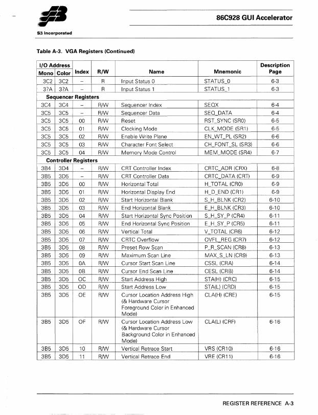
,I. 86C928 GUI Accelerator
53 Incorporated
Table A-3. VGA Registers (Continued)
I/O Address Description
Mono Color Index R/W Name Mnemonic Page
3C2 3C2 - R I nput Status 0 STATUS 0 6-3
3?A 3?A - R Input Status 1 STATUS 1 6-3
Sequencer Registers
3C4 3C4 - R/W Sequencer Index SEQX 6-4
3C5 3C5 - R/W Sequencer Data SEQ DATA 6-4
3C5 3C5 00 R/W Reset RST SYNC (SRO) 6-5
3C5 3C5 01 R/W Clocking Mode CLK MODE (SR1) 6-5
3C5 3C5 02 R/W Enable Write Plane EN WT PL (SR2) 6-6
3C5 3C5 03 R/W Character Font Select CH FONT SL (SR3) 6-6
3C5 3C5 04 R/W Memory Mode Control MEM MODE (SR4) 6-7
Controller Registers
3B4 304 - R/W CRT Controller Index CRTC AOR (CRX) 6-8
3B5 305 - R/W CRT Controller Data CRTC DATA (CRT) 6-9
3B5 305 00 R/W Horizontal Total H TOTAL (CRO) 6-9
3B5 305 01 R/W Horizontal Display End H 0 END (CR1) 6-9
3B5 305 02 R/W Start Horizontal Blank S H BLNK (CR2) 6-10
3B5 305 03 R/W End Horizontal Blank E H BLNK (CR3) 6-10
3B5 305 04 R/W Start Horizontal Sync Position S H SY P (CR4) 6-11
3B5 305 05 R/W End Horizontal Sync Position E H SY P (CR5) 6-11
3B5 305 06 R/W Vertical Total V TOTAL (CR6) 6-12
3B5 305 07 R/W CRTC Overflow OVFL REG (CR7) 6-12
3B5 305 OS R/W Preset Row Scan P R SCAN (CRS) 6-13
3B5 305 09 R/W Maximum Scan Line MAX S LN (CR9) 6-13
3B5 305 OA R/W Cursor Start Scan Line CSSL (CRA) 6-14
3B5 305 OB R/W Cursor End Scan Line CESL (CRB) 6-14
3B5 305 OC R/W Start Address High ST A(H) (CRC) 6-15
3B5 305 00 R/W Start Address Low ST A(L) (CRO) 6-15
3B5 305 OE R/W Cursor Location Address High CLA(H) (CRE) 6-15 (& Hardware Cursor Foreground Color in Enhanced Mode)
3B5 305 OF R/W Cursor Location Address Low CLA(L) (CRF) 6-16 (& Hardware Cursor Background Color in Enhanced Mode)
3B5 305 10 R/W Vertical Retrace Start VRS (CR1 0) 6-16
3B5 305 11 R/W Vertical Retrace End VRE(CR11) 6-16
REGISTER REFERENCE A-3
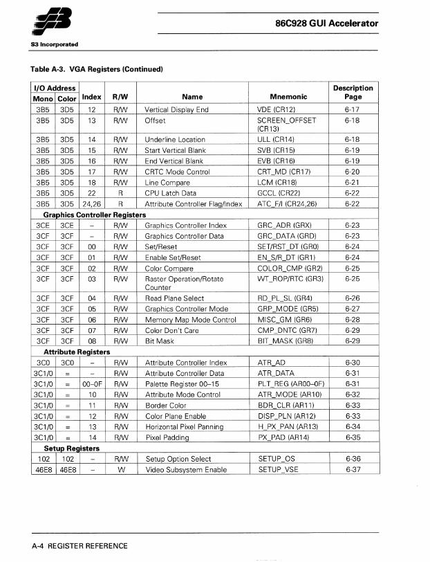
86C928 GUI Accelerator
S3 Incorporated
Table A-3. VGA Registers (Continued)
1/0 Address Description
Mono Color Index R/W Name Mnemonic Page
3B5 3D5 12 RJW Vertical Display End VDE (CR12) 6-17
3B5 3D5 13 R/W Offset SCREEN_OFFSET 6-18 (CR13)
3B5 3D5 14 R/W Underline Location ULL (CR14) 6-18
3B5 3D5 15 R/W Start Vertical Blank SVB (CR15) 6-19
3B5 3D5 16 R/W End Vertical Blank EVB (CR16) 6-19
3B5 3D5 17 R/W CRTC Mode Control CRT MD (CR17) 6-20
3B5 3D5 18 R/W Line Compare LCM (CR18) 6-21
3B5 3D5 22 R CPU Latch Data GCCL (CR22) 6-22
3B5 3D5 24,26 R Attribute Controller Flag/Index ATC F/I (CR24,26) 6-22
Graphics Controller Registers
3CE 3CE - R/W Graphics Controller Index GRC ADR (GRX) 6-23
3CF 3CF - R/W Graphics Controller Data GRC DATA (GRD) 6-23
3CF 3CF 00 R/W Set/Reset SET/RST DT (GRO) 6-24
3CF 3CF 01 R/W Enable Set/Reset EN SIR DT (GR1) 6-24
3CF 3CF 02 R/W Color Compare COLOR CMP (GR2) 6-25
3CF 3CF 03 R/W Raster Operation/Rotate WT_ROP/RTC (GR3) 6-25 Counter
3CF 3CF 04 R/W Read Plane Select RD PL SL (GR4) 6-26
3CF 3CF 05 R/W Graphics Controller Mode GRP MODE (GR5) 6-27
3CF 3CF 06 R/W Memory Map Mode Control MISC GM (GR6) 6-28
3CF 3CF 07 R/W Color Don't Care CMP DNTC (GR7) 6-29
3CF 3CF 08 R/W Bit Mask BIT MASK (GR8) 6-29
Attribute Registers
3CO 3CO - R/W Attribute Controller Index ATR AD 6-30
3Cl/0 = - R/W Attribute Controller Data ATR DATA 6-31
3Cl/0 = OO-OF R/W Palette Register 00-15 PL T REG (AROO--DF) 6-31
3Cl/0 = 10 R/W Attribute Mode Control ATR MODE (ARlO) 6-32
3Cl/0 = 11 R/W Border Color BDR CLR (ARll) 6-33
3Cl/0 = 12 R/W Color Plane Enable DISP PLN (AR12) 6-33
3Cl/0 = 13 R/W Horizontal Pixel Panning H PX PAN (AR13) 6-34
3Cl/0 = 14 R/W Pixel PaddinQ PX PAD (AR14) 6-35
Setup Re~ isters 102 102 - R/W Setup OPtion Select SETUP OS 6-36
46E8 46E8 - W Video Subsystem Enable SETUP VSE 6-37
A-4 REGISTER REFERENCE
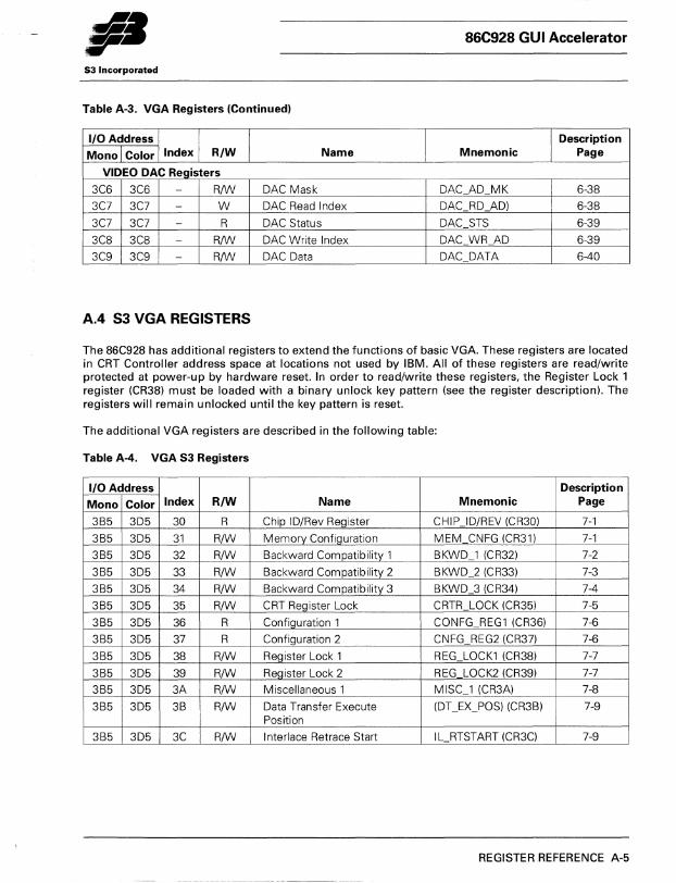
86C928 GUI Accelerator
53 Incorporated
Table A-3. VGA Registers (Continued)
I/O Address Description
Mono Color Index R/W Name Mnemonic Page
VIDEO DAC Registers
3C6 3C6 - R/W DAC Mask DAC AD MK 6-38
3C7 3C7 - W DAC Read Index DAC RD AD) 6-38
3C7 3C7 - R DAC Status DAC STS 6-39
3C8 3C8 - R/W DAC Write Index DAC WR AD 6-39
3C9 3C9 - R/W DAC Data DAC DATA 6-40
A.4 S3 VGA REGISTERS
The 86C928 has additional registers to extend the functions of basic VGA. These registers are located in CRT Controller address space at locations not used by IBM. All of these registers are read/write protected at power-up by hardware reset. In order to read/write these registers, the Register Lock 1 register (CR38) must be loaded with a binary unlock key pattern (see the register description). The registers will remain unlocked until the key pattern is reset.
The additional VGA registers are described in the following table:
Table A-4. VGA S3 Registers
I/O Address Description
Mono Color Index R/W Name Mnemonic Page
3B5 3D5 30 R Chip ID/Rev Register CHIP ID/REV (CR30) 7-1
3B5 3D5 31 R/W Memorv Confiquration MEM CNFG (CR31) 7-1
3B5 3D5 32 R/W Backward Compatibility 1 BKWD 1 (CR32) 7-2
3B5 3D5 33 R/W Backward Compatibility 2 BKWD 2 (CR33) 7-3
3B5 3D5 34 R/W Backward Compatibility 3 BKWD 3 (CR34) 7-4
3B5 3D5 35 R/W CRT Register Lock CRTR LOCK (CR35) 7-5
3B5 3D5 36 R Configuration 1 CONFG REG1 (CR36) 7-6
3B5 3D5 37 R Configuration 2 CNFG REG2 (CR37) 7-6
3B5 3D5 38 R/W Register Lock 1 REG LOCK1 (CR38) 7-7
3B5 3D5 39 R/W Reqister Lock 2 REG LOCK2 (CR39) 7-7
3B5 3D5 3A R/W Miscellaneous 1 MISC 1 (CR3A) 7-8
3B5 3D5 3B R/W Data Transfer Execute (DT_EX_POS) (CR3B) 7-9 Position
3B5 3D5 3C R/W I nterlace Retrace Start I L RTST ART (CR3C) 7-9
REGISTER REFERENCE A-5
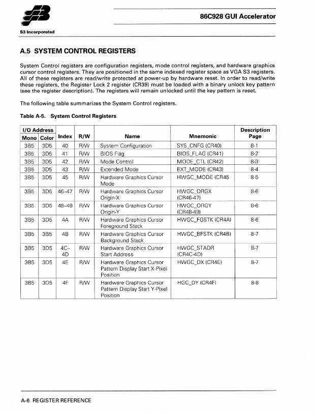
fl· 86C928 GUI Accelerator
S3 Incorporated
A.5 SYSTEM CONTROL REGISTERS
System Control registers are configuration registers, mode control registers, and hardware graphics cursor control registers. They are positioned in the same indexed register space as VGA S3 registers. All of these registers are read/write protected at power-up by hardware reset. In order to read/write these registers, the Register Lock 2 register (CR39) must be loaded with a binary unlock key pattern (see the register description). The registers will remain unlocked until the key pattern is reset.
The following table summarizes the System Control registers.
Table A-5. System Control Registers
I/O Address Description
Mono Color Index R/W Name Mnemonic Page
3B5 3D5 40 RNJ System Configuration SYS CNFG (CR40) 8-1
3B5 3D5 41 RNJ BIOS Flag BIOS FLAG (CR41) 8-2
3B5 3D5 42 RNJ Mode Control MODE CTL (CR42) 8-3
3B5 3D5 43 RNJ Extended Mode EXT MODE (CR43) 8-4
3B5 3D5 45 RNJ Hardware Graphics Cursor HWGCMODE (CR45 8-5 Mode
3B5 3D5 46-47 RNJ Hardware Graphics Cursor HWGCORGX 8-6 Origin-X (CR46-47)
3B5 3D5 48-49 RNJ Hardware Graphics Cursor HWGC_ORGY 8-6 Oriqin-Y (CR48-49)
3B5 3D5 4A RNJ Hardware Graphics Cursor HWGC_FGSTK (CR4A) 8-6 Foreground Stack
3B5 3B5 4B RNJ Hardware Graphics Cursor HWGC_BFSTK (CR4B) 8-7 Backqround Stack
3B5 3D5 4C- R/W Hardware Graphics Cursor HWGC_STADR 8-7 4D Start Address (CR4C-4D)
3B5 3D5 4E RNJ Hardware Graphics Cursor HWGCDX (CR4E) 8-7 Pattern Display Start X-Pixel Position
3B5 3D5 4F RNJ Hardware Graphics Cursor HGC_DY (CR4F) 8-8 Pattern Display Start Y-Pixel Position
A-6 REGISTER REFERENCE
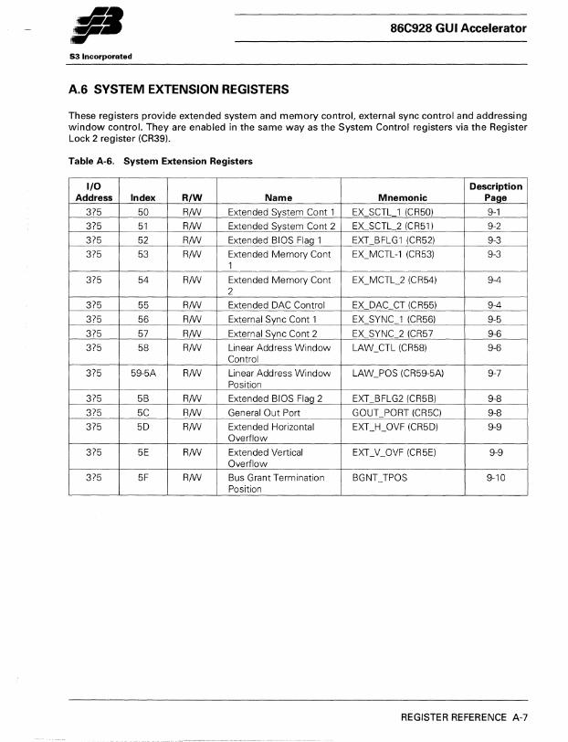
86C928 GUI Accelerator
53 Incorporated
A.6 SYSTEM EXTENSION REGISTERS
These registers provide extended system and memory control, external sync control and addressing window control. They are enabled in the same way as the System Control registers via the Register Lock 2 register (CR39).
Table A-S. System Extension Registers
I/O Description Address Index R/W Name Mnemonic Page
375 50 RNI/ Extended S,{stem Cont 1 EX SCTL 1 (CR50) 9-1
375 51 RNI/ Extended System Cont 2 EX SCTL 2 (CR51) 9-2
375 52 RNI/ Extended BIOS Flag 1 EXT BFLG1 (CR52) 9-3
375 53 RNI/ Extended Memory Cont EX_MCTL-1 (CR53) 9-3 1
375 54 RNI/ Extended Memory Cont EX_MCTL_2 (CR54) 9-4 2
375 55 RNI/ Extended DAC Control EX OAC CT (CR55) 9-4
375 56 RNI/ Extemal Sync Cont 1 EX SYNC 1 (CR56) 9-5
375 57 RNI/ External Sync Cont 2 EX SYNC 2 (CR57 9-6
375 58 RNI/ Linear Address Window LAW_CTL (CR58) 9-6 Control
375 59-5A RNI/ Linear Address Window LAW_POS (CR59-5A) 9-7 Position
375 5B RNI/ Extended BIOS Flag 2 EXT BFLG2 (CR5B) 9-8
375 5C RNI/ General Out Port GOUT PORT (CR5C) 9-8
375 50 RNI/ Extended Horizontal EXT _H_OVF (CR50) 9-9 Overflow
375 5E RNI/ Extended Vertical EXT _ V _ OVF (CR 5E) 9-9 Overflow
375 5F RNI/ Bus Grant Termination BGNT_TPOS 9-10 Position
REGISTER REFERENCE A-7
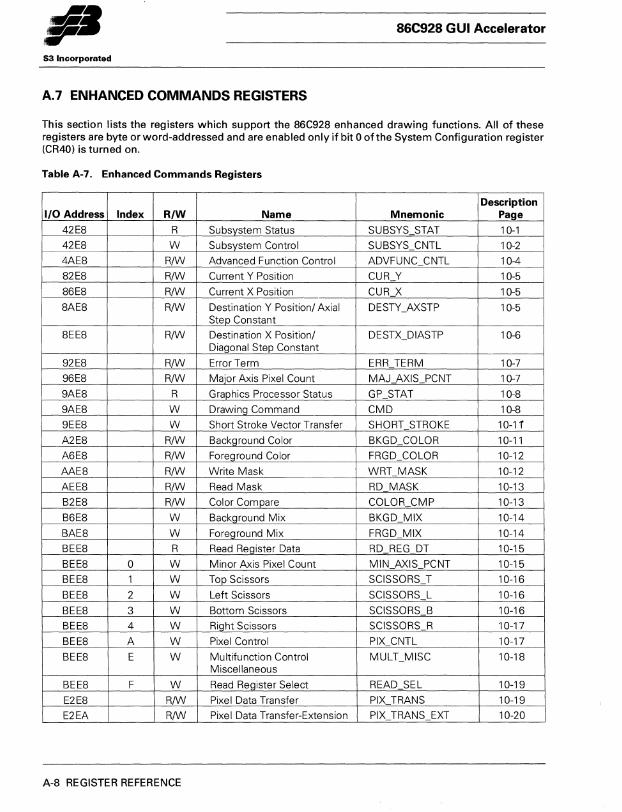
II· 86C928 GUI Accelerator
S3 Incorporated
A.7 ENHANCED COMMANDS REGISTERS
This section lists the registers which support the 86C928 enhanced drawing functions. All of these registers are byte or word-addressed and are enabled only if bit 0 ofthe System Configuration register (CR40) is turned on.
Table A-7. Enhanced Commands Registers
Description I/O Address Index R/W Name Mnemonic Page
42E8 R Subsystem Status SUBSYS STAT 10-1 42E8 W Subsystem Control SUBSYS CNTl 10-2
4AE8 R/W Advanced Function Control ADVFUNC CNTl 10-4
82E8 R/W Current Y Position CUR Y 10-5
86E8 R/W Current X Position CUR X 10-5
8AE8 R/W Destination Y Position/ Axial DESTY_AXSTP 10-5 Step Constant
8EE8 R/W Destination X Position/ DESTX_DIASTP 10-6 Diagonal Step Constant
92E8 R/W Error Term ERR TERM 10-7
96E8 R/W Major Axis Pixel Count MAJ AXIS PCNT 10-7
9AE8 R Graphics Processor Status GP STAT 10-8
9AE8 W Drawinq Command CMD 10-8
9EE8 W Short Stroke Vector Transfer SHORT STROKE 10-1 i A2E8 R/W Background Color BKGD COLOR 10-11
A6E8 R/W Foreground Color FRGD COLOR 10-12
AAE8 R/W Write Mask WRT MASK 10-12 ----AEE8 R/W Read Mask RD MASK 10-13
B2E8 R/W Color Compare COLOR CMP 10-13
B6E8 W Background Mix BKGD MIX 10-14
BAE8 W Foreqround Mix FRGD MIX 10-14
BEE8 R Read Register Data RD REG DT 10-15
BEE8 0 W Minor Axis Pixel Count MIN AXIS PCNT 10-15
BEE8 1 W Top Scissors SCISSORS T 10-16
BEE8 2 W left Scissors SCISSORS l 10-16
BEE8 3 W Bottom Scissors SCISSORS B 10-16
BEE8 4 W Right Scissors SCISSORS R 10-17
BEE8 A W Pixel Control PIX CNTl 10-17
BEE8 E W Mu Itifu nction Control MUlT_MISC 10-18 Miscellaneous
BEE8 F W Read Register Select READ SEl 10-19
E2E8 R/W Pixel Data Transfer PIX TRANS 10-19
E2EA R/W Pixel Data Transfer-Extension PIX TRANS EXT 10-20
A-8 REGISTER REFERENCE

86C928 GUI Accelerator
S3 Incorporated

86C928 GUI Accelerator
53 Incorporated
S3 Incorporated, 2880 San Tomas Expressway, Santa Clara, CA 95051-0981 Tel: 408-980-5400, Fax: 408-980-5444
Printed in USA DB02-C

53 Incorporated
2880 San Tomas Expwy.
Santa Clara, CA 95051-0981
Tel: (408) 980-5400
Fax: (408) 980-5444
Printed in U.S.A. 0 802-C
Related Documents


