Welcome message from author
This document is posted to help you gain knowledge. Please leave a comment to let me know what you think about it! Share it to your friends and learn new things together.
Transcript


Function is similar to software designed counters & Timers
Generate time delays Applications:
Real time clock, Event Counter, Square wave generator, Complex waveform generator

Features:1.24 DIP2.+5V supply3.3 16 bit counters4.6 modes of operation5. At the end of the count the pulse is
generated which interrupt the MPU.


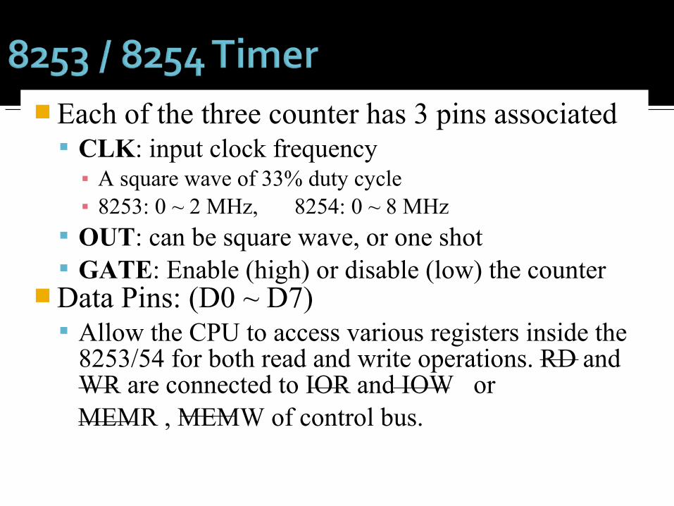
Each of the three counter has 3 pins associated CLK: input clock frequency▪ A square wave of 33% duty cycle▪ 8253: 0 ~ 2 MHz, 8254: 0 ~ 8 MHz
OUT: can be square wave, or one shot GATE: Enable (high) or disable (low) the counter
Data Pins: (D0 ~ D7) Allow the CPU to access various registers inside the
8253/54 for both read and write operations. RD and WR are connected to IOR and IOW or
MEMR , MEMW of control bus.
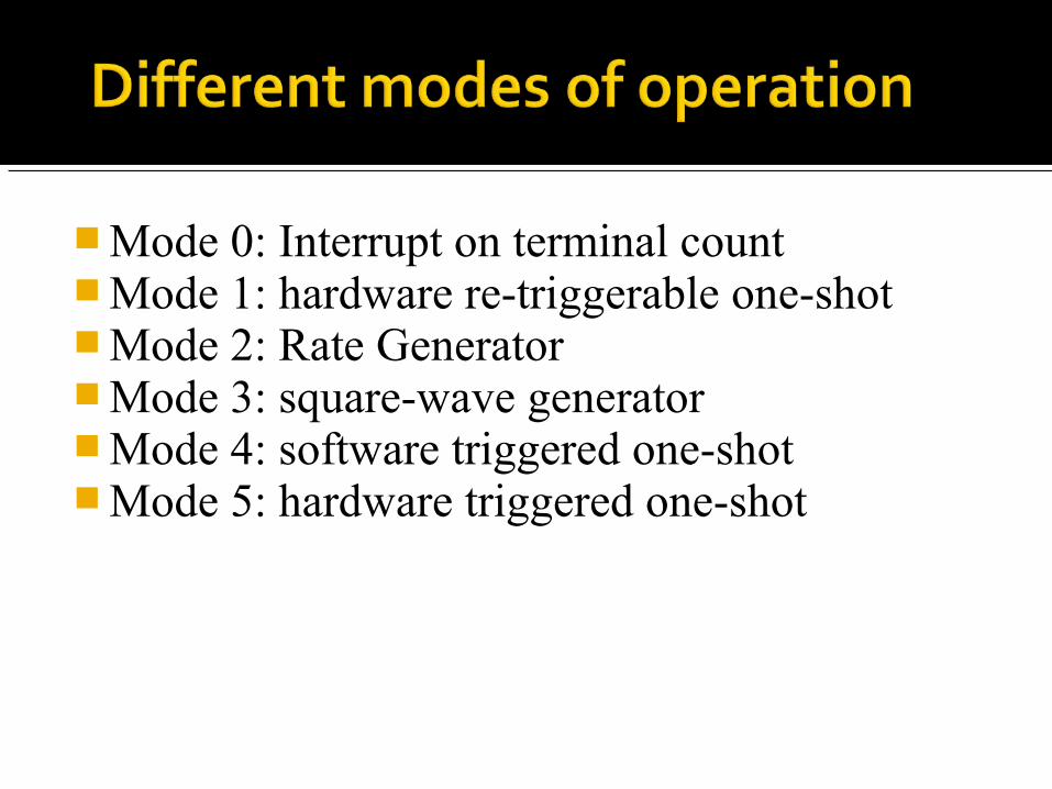
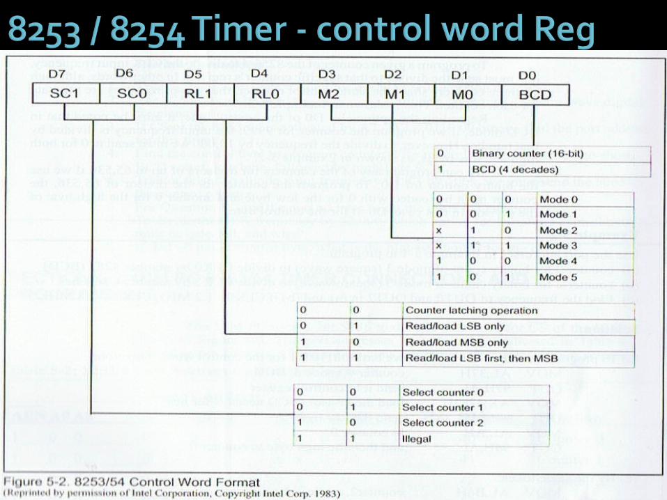
Mode 0: Interrupt on terminal count Mode 1: hardware re-triggerable one-shot Mode 2: Rate Generator Mode 3: square-wave generator Mode 4: software triggered one-shot Mode 5: hardware triggered one-shot

It is used for event counting. After control word is written, OUT is initially low
and will remain low until counter reaches zero. OUT then goes high and remains high until a new
count or new mode 0 control word is written into the counter.
GATE=1 enables counting; GATE=0 disables counting. GATE has no effect on OUT.
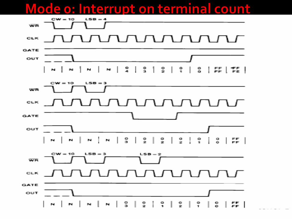

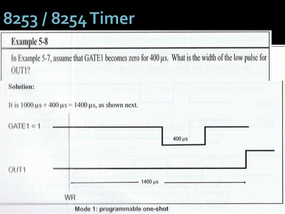
Mode 0: Interrupt on terminal count If GATE becomes low at the middle of the count, the
count will stop and the output will be low. The count resumes when the GATE becomes high again This in effect adds to the total time the output is low.
Mode 1: HW triggered / programmable one shot The triggering must be done through the GATE input
by sending a 0-to-1 pulse to it. Steps: 1) Load the count register
2) A 0-to-1 pulse must be sent to the GATE input to trigger the count

Mode 1: HW triggered / programmable one shot In this mode, OUT is initially high When the GATE is triggered, the OUT goes low and
at the end of the count the OUT goes high again, thus generating a one shot pulse.

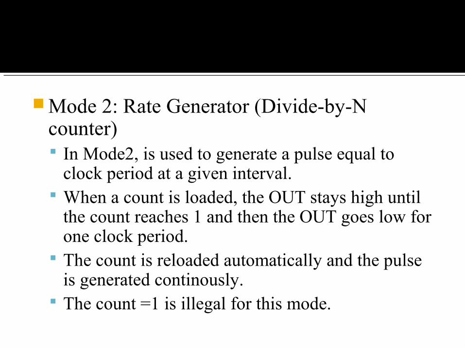
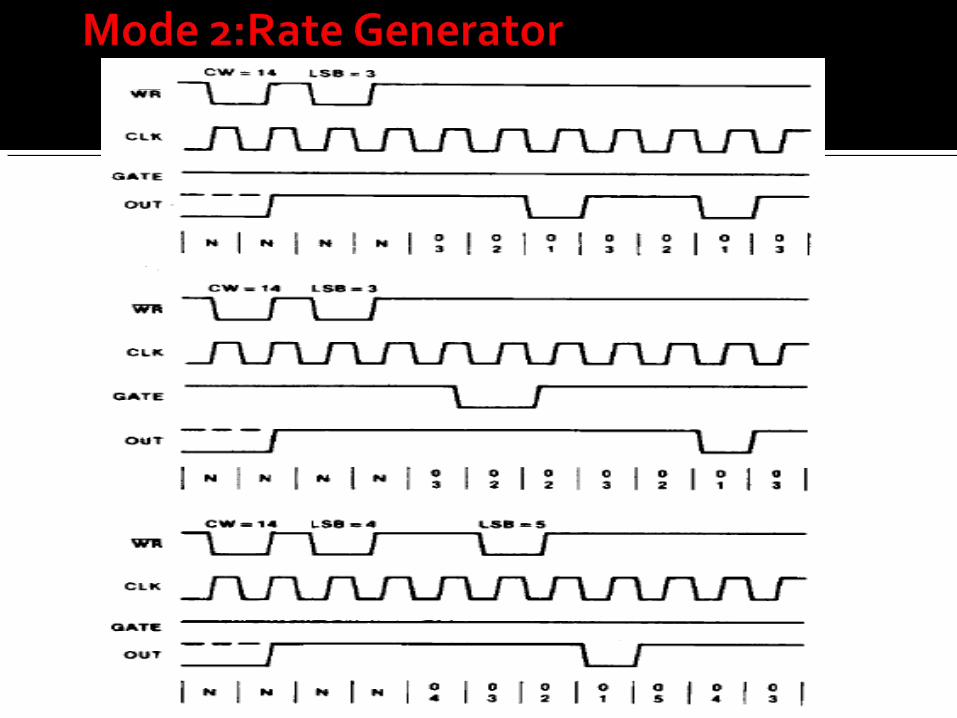
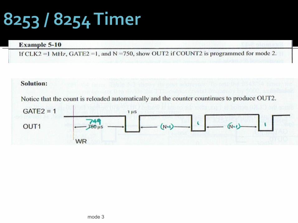
Mode 2: Rate Generator (Divide-by-N counter) In Mode2, is used to generate a pulse equal to
clock period at a given interval. When a count is loaded, the OUT stays high until
the count reaches 1 and then the OUT goes low for one clock period.
The count is reloaded automatically and the pulse is generated continously.
The count =1 is illegal for this mode.

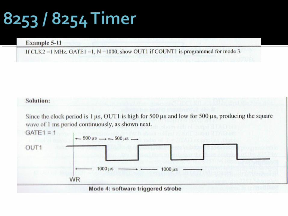
Mode 3: Square wave rate generator When the count is loaded, the OUT is high. The count is decremented by two at every clock
cycle and when it reaches zero the OUT goes low, and the count is reloaded again.
If the count is odd the pulse will stay high for (N+1)/2 and low for (N-1)/2.

Mode 4: Software triggered strobe OUT is initially high It goes low for one clock period at the end of the
count. The count must be reloaded for subsequent
counts.

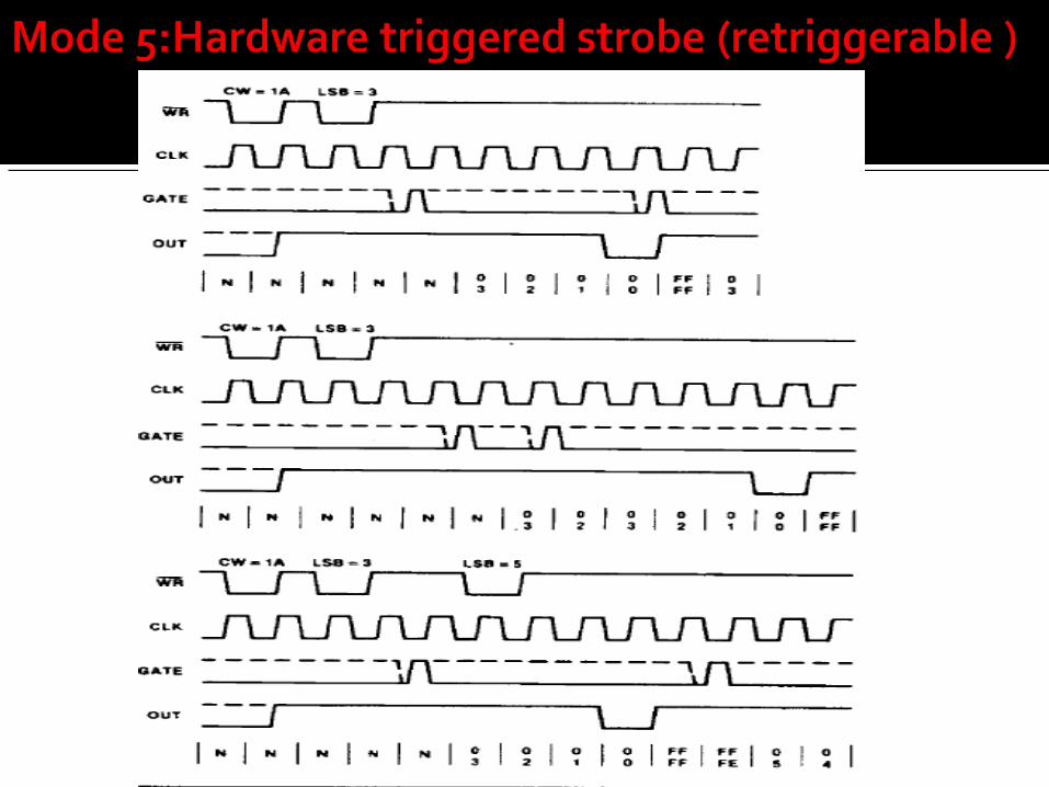
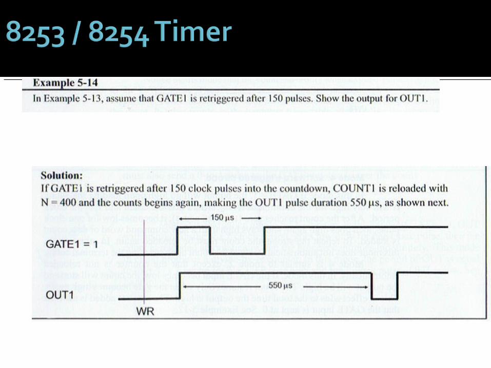
Mode 5: Hardware triggered strobe Similar to Mode4, except that the triggering must be
done with the GATE input The count starts only when a 0-to-1 pulse is sent to
the GATE input If GATE retriggered during the counting, it will restart
the down counting

Task1: program counter 0 for binary counter for mode 3 to divide CLK0 by number 4282 (BCD)MOV AL, 0011 0111BOUT 97H, ALMOV AX, 4282H (BCD needs H)OUT 94H, AL (Low Byte)MOV AL, AHOUT 94H, AL (High Byte)
OUT0 = CLK0 / 4282
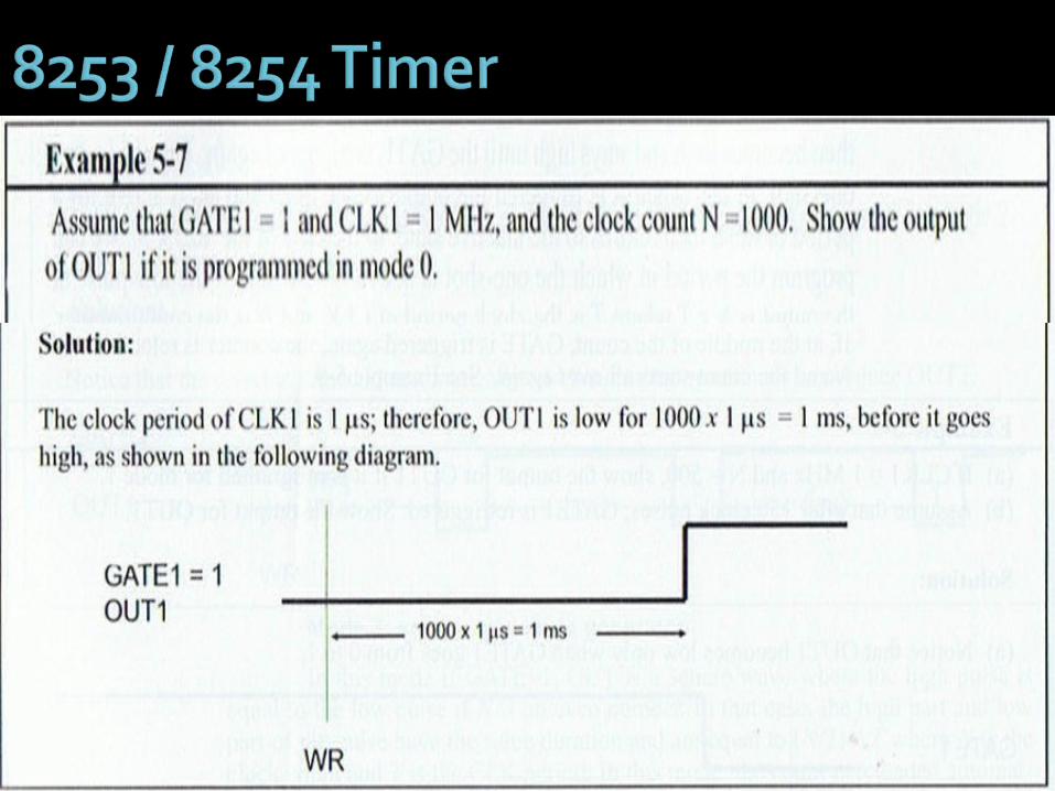
Mode 0: Interrupt on terminal count The output is initially low, and remain low for the
duration of the count if GATE=1. When the terminal count is reached, the output will go high and remain high until a new control word or new count number is loaded▪ Width of low pulse = N * T, where T is clock period
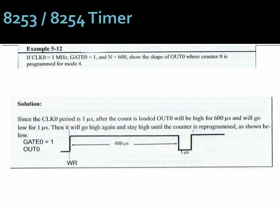
Example: GATE=1 and CLK = 1 MHzClock count N = 1000

mode 3


Memory Fundamentals In all computer designs, semiconductor memories are
used as primary storage for code and data Requirement of primary memory Fast in
responding to CPU Types: RAM and ROM Memory capacity
▪ The capacity of a memory IC chip is always given in bits▪ Chip capacity: the number of bits that a chip can store: Kbits, Mbits
▪ The capacity of a computer is given in bytes▪ Example: A 4M chip – 4M bits, A 4M computer – 4M bytes

Memory organization▪ Memory chips are organized into a number of locations
within the IC▪ The number of bits that each location can hold is always
equal to the number of data pins on the chip▪ How many locations exist inside a memory map?
That depends on the number of address pins Given x the number of address pins 2x locations
▪ The total number of bits that a memory chip can store is equal to the number of locations times the number of data bits per location

Speed▪ The speed of a memory chip is commonly referred to as its
access time, varied from a few ns to hundreds of us.
Characteristics▪ Capacity, Organization, Speed
Examples▪ 256 K memory chip with 8 data pins
▪ Organization: 32K * 8 / Address: 15pins
▪ A memory chip has 13 address lines and 4 data lines▪ Organization: 213 * 4 = 8K * 4 = 32Kbits
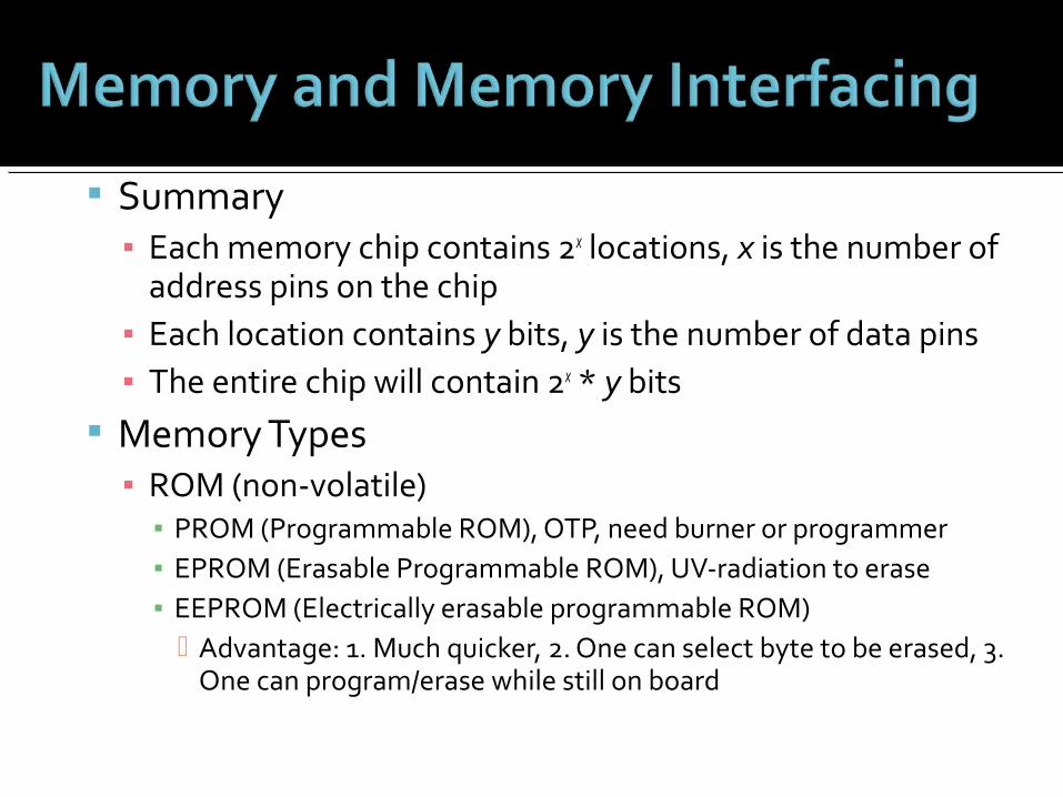
Summary▪ Each memory chip contains 2x locations, x is the number of
address pins on the chip▪ Each location contains y bits, y is the number of data pins ▪ The entire chip will contain 2x * y bits
Memory Types▪ ROM (non-volatile)
▪ PROM (Programmable ROM), OTP, need burner or programmer▪ EPROM (Erasable Programmable ROM), UV-radiation to erase▪ EEPROM (Electrically erasable programmable ROM)
Advantage: 1. Much quicker, 2. One can select byte to be erased, 3. One can program/erase while still on board
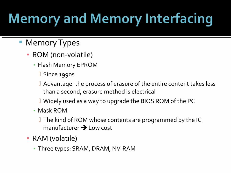
Memory Types▪ ROM (non-volatile)
▪ Flash Memory EPROM Since 1990s Advantage: the process of erasure of the entire content takes less
than a second, erasure method is electrical Widely used as a way to upgrade the BIOS ROM of the PC
▪ Mask ROM The kind of ROM whose contents are programmed by the IC
manufacturer Low cost
▪ RAM (volatile)▪ Three types: SRAM, DRAM, NV-RAM
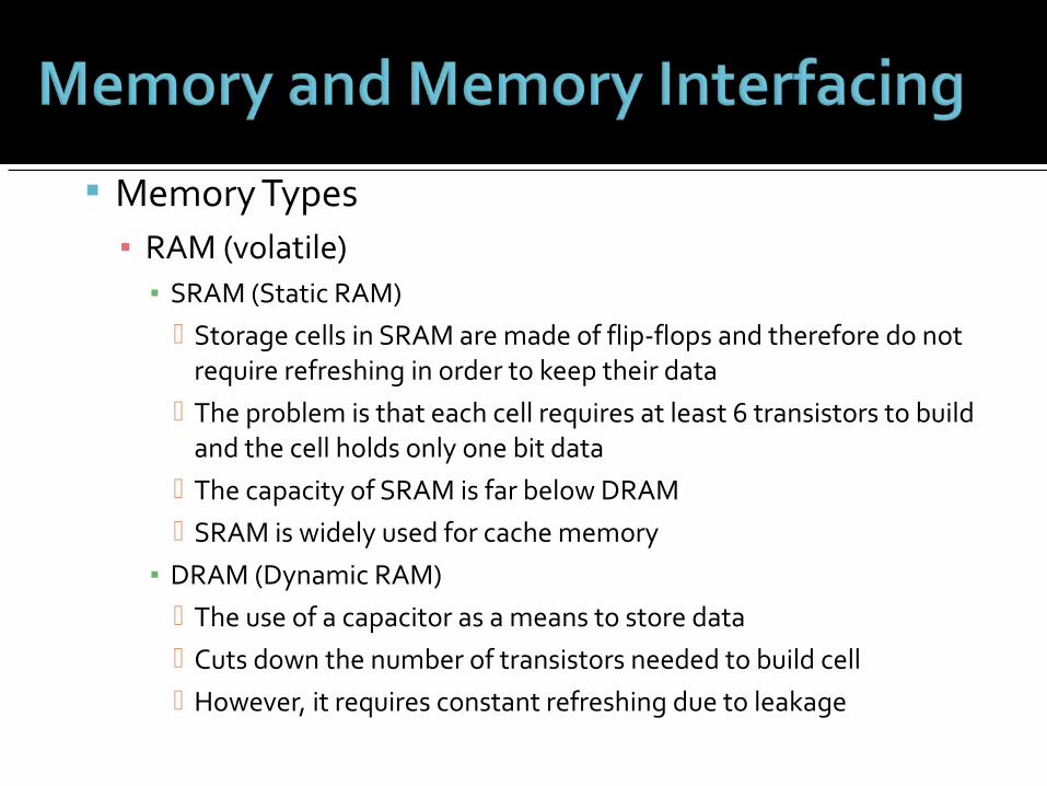
Memory Types▪ RAM (volatile)
▪ SRAM (Static RAM) Storage cells in SRAM are made of flip-flops and therefore do not
require refreshing in order to keep their data The problem is that each cell requires at least 6 transistors to build
and the cell holds only one bit data The capacity of SRAM is far below DRAM SRAM is widely used for cache memory
▪ DRAM (Dynamic RAM) The use of a capacitor as a means to store data Cuts down the number of transistors needed to build cell However, it requires constant refreshing due to leakage
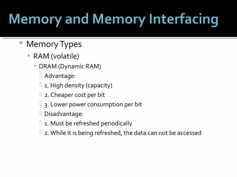
Memory Types▪ RAM (volatile)▪ DRAM (Dynamic RAM)
Advantage: 1. High density (capacity) 2. Cheaper cost per bit 3. Lower power consumption per bit Disadvantage: 1. Must be refreshed periodically 2. While it is being refreshed, the data can not be accessed
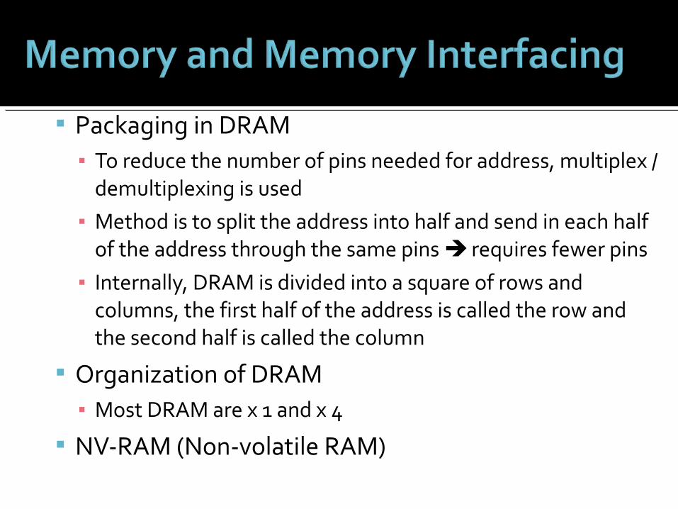
Packaging in DRAM▪ To reduce the number of pins needed for address, multiplex /
demultiplexing is used▪ Method is to split the address into half and send in each half
of the address through the same pins requires fewer pins▪ Internally, DRAM is divided into a square of rows and
columns, the first half of the address is called the row and the second half is called the column
Organization of DRAM▪ Most DRAM are x 1 and x 4
NV-RAM (Non-volatile RAM)
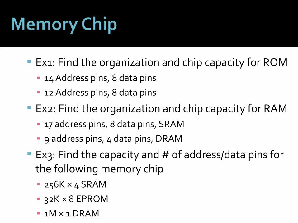
Ex1: Find the organization and chip capacity for ROM▪ 14 Address pins, 8 data pins ▪ 12 Address pins, 8 data pins
Ex2: Find the organization and chip capacity for RAM▪ 17 address pins, 8 data pins, SRAM▪ 9 address pins, 4 data pins, DRAM
Ex3: Find the capacity and # of address/data pins for the following memory chip▪ 256K × 4 SRAM▪ 32K × 8 EPROM▪ 1M × 1 DRAM
Typical 8086/8088 Machine Instruction Format
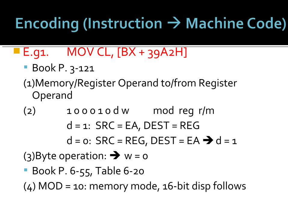
E.g1. MOV CL, [BX + 39A2H] Book P. 3-121(1)Memory/Register Operand to/from Register
Operand(2) 1 0 0 0 1 0 d w mod reg r/m
d = 1: SRC = EA, DEST = REGd = 0: SRC = REG, DEST = EA d = 1
(3)Byte operation: w = 0 Book P. 6-55, Table 6-20(4) MOD = 10: memory mode, 16-bit disp follows
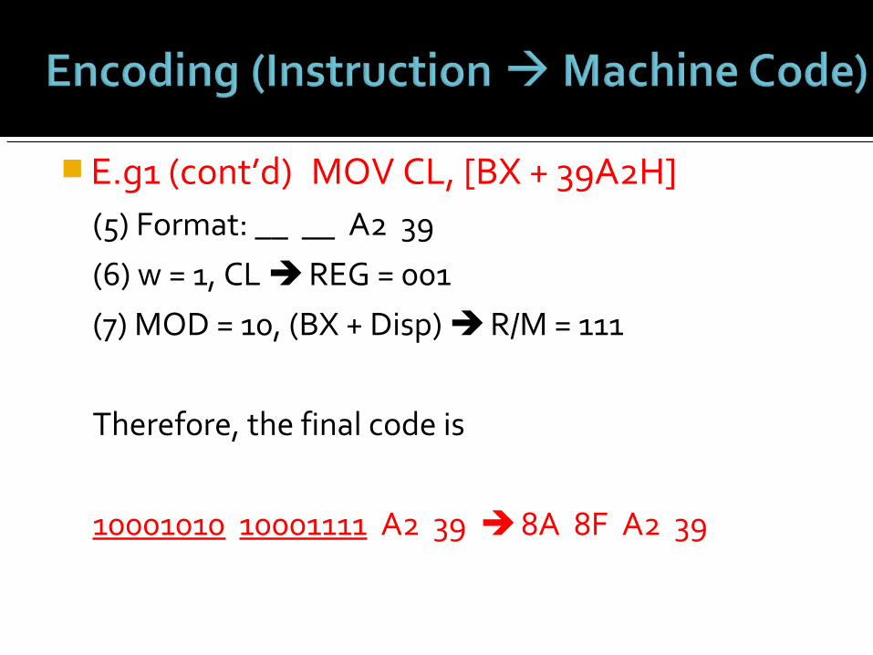
E.g1 (cont’d) MOV CL, [BX + 39A2H](5) Format: __ __ A2 39(6) w = 1, CL REG = 001(7) MOD = 10, (BX + Disp) R/M = 111
Therefore, the final code is
10001010 10001111 A2 39 8A 8F A2 39

E.g2. ADD WORD PTR ES: [BX + SI + 1053H], AX
(1)Override operation: we need to put a overrode prefix before the machine code Book P. 6-61(2) 0 0 1 reg 1 1 0 SEGMENT = override prefix Book P. 6-56(3) ES: 00 CS: 01 SS: 10 DS:11 Book P. 6-61(4) Therefore the prefix is: 0 0 1 0 0 1 1 0 (26H)

E.g2. ADD WORD PTR ES: [BX + SI + 1053H], AX Book P. 3-64(5) Memory/register Operand with Register Operand
0 0 0 0 0 0 d w mod reg r/md = 1: LSRC=REG, RSRC=EA, DEST=REGd = 0: LSRC=EA, RSRC=REG, DEST=EA d = 0(6) Word operation w = 1 Book P. 6-55, Table 6-18(7) 16-bit Disp mod = 10(8) Reg: AX Reg = 000, R/M = 000Therefore, 00100110 00000001 10000000 53 10
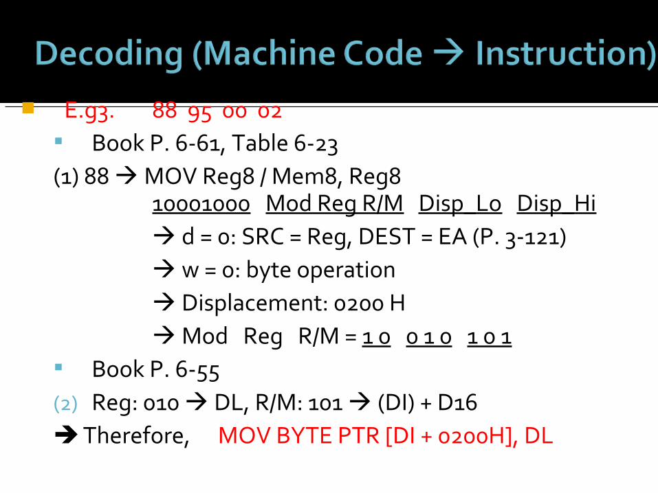
E.g3. 88 95 00 02 Book P. 6-61, Table 6-23(1) 88 MOV Reg8 / Mem8, Reg8
10001000 Mod Reg R/M Disp_Lo Disp_Hi d = 0: SRC = Reg, DEST = EA (P. 3-121) w = 0: byte operation Displacement: 0200 H Mod Reg R/M = 1 0 0 1 0 1 0 1
Book P. 6-55(2) Reg: 010 DL, R/M: 101 (DI) + D16 Therefore, MOV BYTE PTR [DI + 0200H], DL
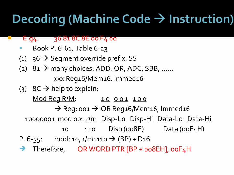
E.g4. 36 81 8C 8E 00 F4 00 Book P. 6-61, Table 6-23(1) 36 Segment override prefix: SS(2) 81 many choices: ADD, OR, ADC, SBB, ……
xxx Reg16/Mem16, Immed16(3) 8C help to explain:
Mod Reg R/M: 1 0 0 0 1 1 0 0 Reg: 001 OR Reg16/Mem16, Immed16
10000001 mod 001 r/m Disp-Lo Disp-Hi Data-Lo Data-Hi 10 110 Disp (008E) Data (00F4H)
P. 6-55: mod: 10, r/m: 110 (BP) + D16 Therefore, OR WORD PTR [BP + 008EH], 00F4H

Practice Question:C7 C7 A9 12 3B 47 F4
MOV DI, 12A9HCMP AX, [BX - 12]
B8 00 02 8E D8 B9 08 00 E2 FEMOV AX, 0200HMOV DS, AXMOV CX, 0008here: LOOP here