Microprocessor and Microcontroller Interfacing 1 8085 Microprocessor Architecture and Memory Interfacing

Welcome message from author
This document is posted to help you gain knowledge. Please leave a comment to let me know what you think about it! Share it to your friends and learn new things together.
Transcript

Microprocessor and Microcontroller Interfacing
11
8085 Microprocessor Architecture and
Memory Interfacing

Microprocessor and Microcontroller Interfacing
22
Points to be Discussed
• 8085 Microprocessor
• 8085 Microprocessor (CPU) Block Diagram
• Control & Status Signals
• Interrupt Signals
• 8085 Microprocessor Signal Flow Diagram
• 8085 Microprocessor Pin Diagram
• Demultiplexing the AD7 to AD0
• Generation of Control Signals
• 8085 Single-Board Microcomputer System
• Data Flow from Memory to MPU
• Instruction cycle, Machine cycle & T-state
• Timing Diagram for executing MVI A,32H
• Timing Diagram of Memory Read Cycle
• Timing Diagram of Memory Write Cycle
• Any Quarries?

Microprocessor and Microcontroller Interfacing
33
8085 Microprocessor
• 8-bit Microprocessor.
• The device has 40 pins.
• Clock frequency = 3MHz.
• Internally crystal frequency is divided by 2. So to operate at 3MHz, crystal frequency must be 6MHz.
• 8085A-2 version supports clock frequency 0f 5MHz.
• 64K Byte addressable memory.

Microprocessor and Microcontroller Interfacing
44
8085 Microprocessor (CPU) Block Diagram
ALU

Microprocessor and Microcontroller Interfacing
55
Control & Status Signals

Microprocessor and Microcontroller Interfacing
66
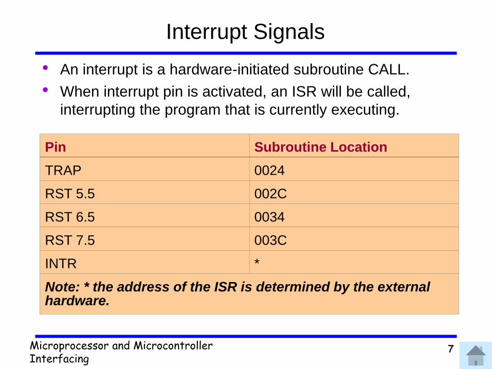
Interrupt Signals
• 8085 μp has several interrupt signals as shown in the following table.
Microprocessor and Microcontroller Interfacing
77
Interrupt Signals
• An interrupt is a hardware-initiated subroutine CALL.
• When interrupt pin is activated, an ISR will be called,
interrupting the program that is currently executing.
Pin Subroutine Location
TRAP 0024
RST 5.5 002C
RST 6.5 0034
RST 7.5 003C
INTR *
Note: * the address of the ISR is determined by the external hardware.
Microprocessor and Microcontroller Interfacing
88
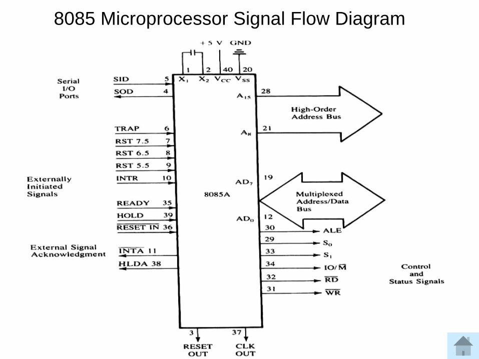
8085 Microprocessor Signal Flow Diagram
Microprocessor and Microcontroller Interfacing
99
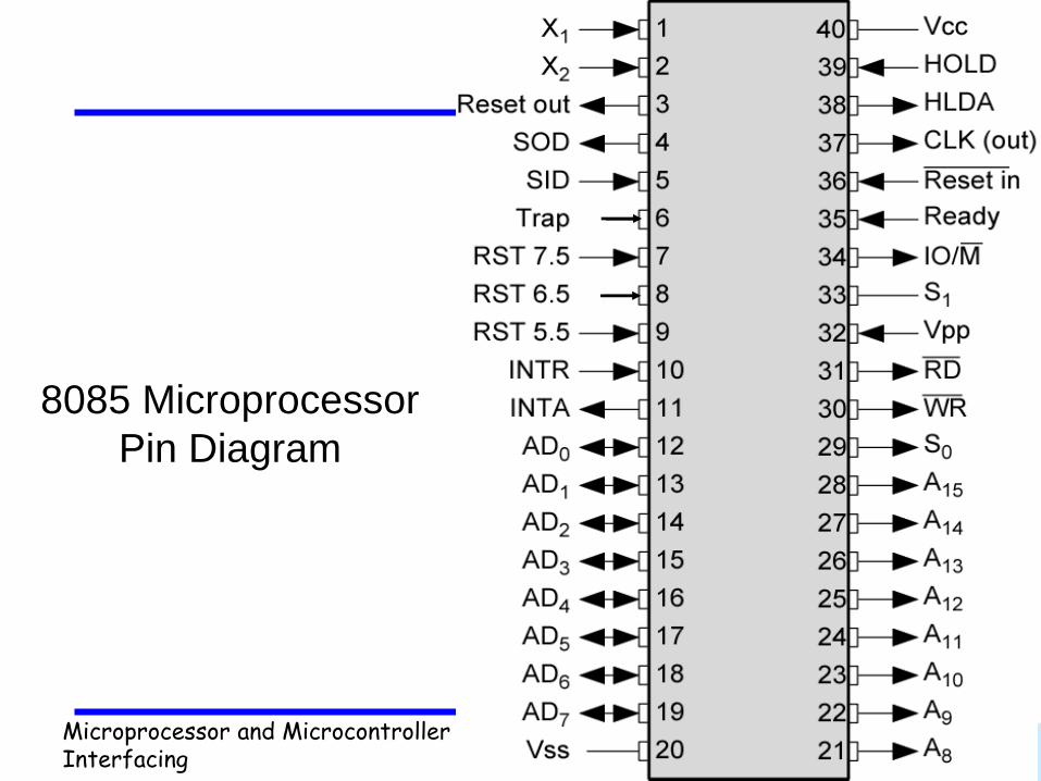
8085 Microprocessor
Pin Diagram

Microprocessor and Microcontroller Interfacing
1010
Demultiplexing the AD7 to AD0

Microprocessor and Microcontroller Interfacing
1111
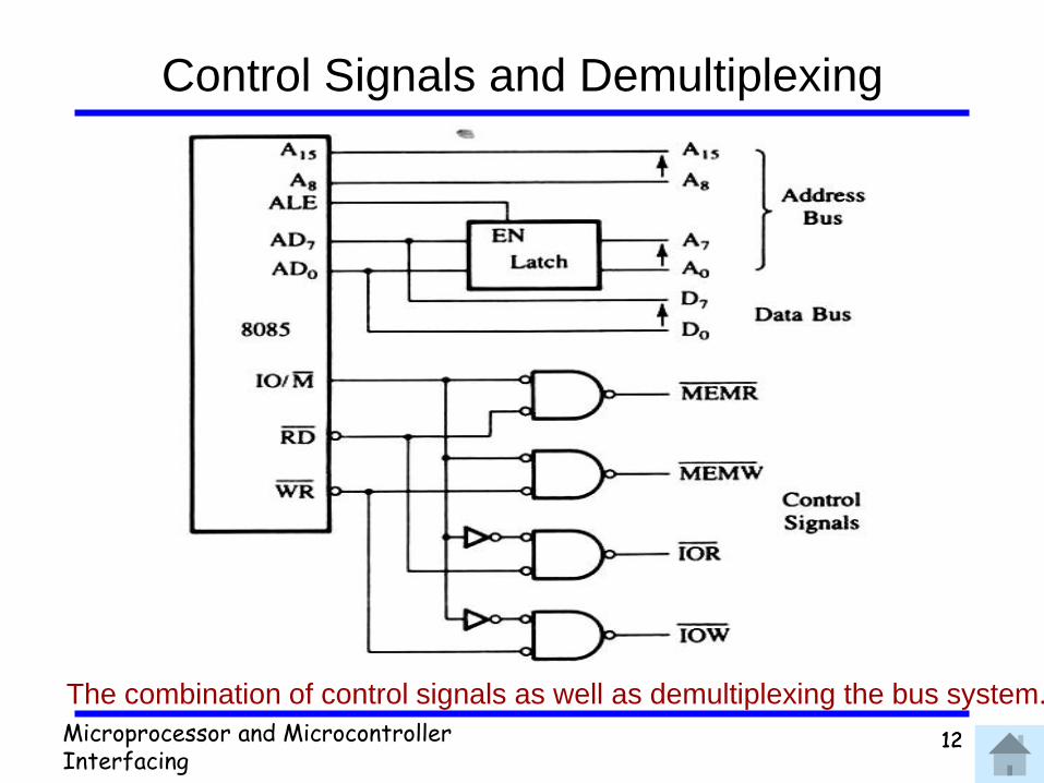
Generation of Control Signals
Example of schematic diagram to generate control signals.
Microprocessor and Microcontroller Interfacing
1212
Control Signals and Demultiplexing
The combination of control signals as well as demultiplexing the bus system.
Microprocessor and Microcontroller Interfacing
13
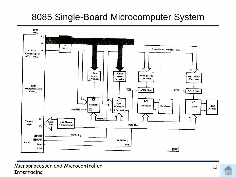
8085 Single-Board Microcomputer System
Microprocessor and Microcontroller Interfacing
1414
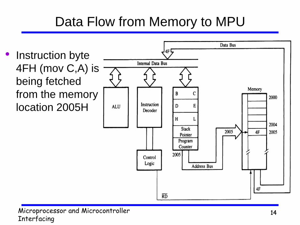
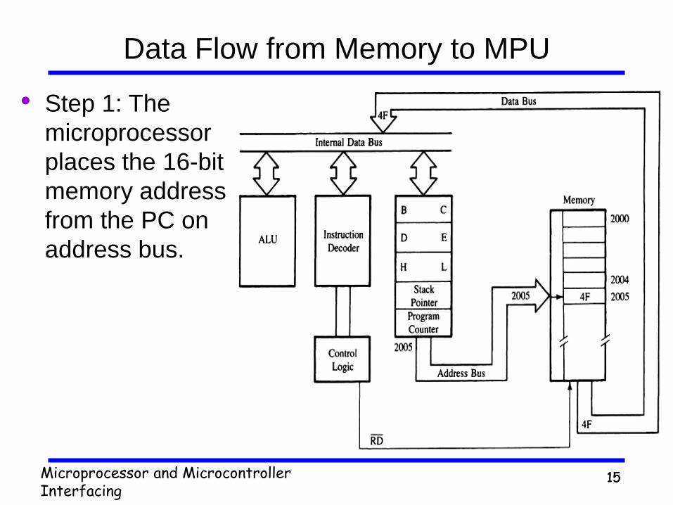
Data Flow from Memory to MPU
• Instruction byte
4FH (mov C,A) is
being fetched
from the memory
location 2005H
Microprocessor and Microcontroller Interfacing
1515
• Step 1: The
microprocessor
places the 16-bit
memory address
from the PC on
address bus.
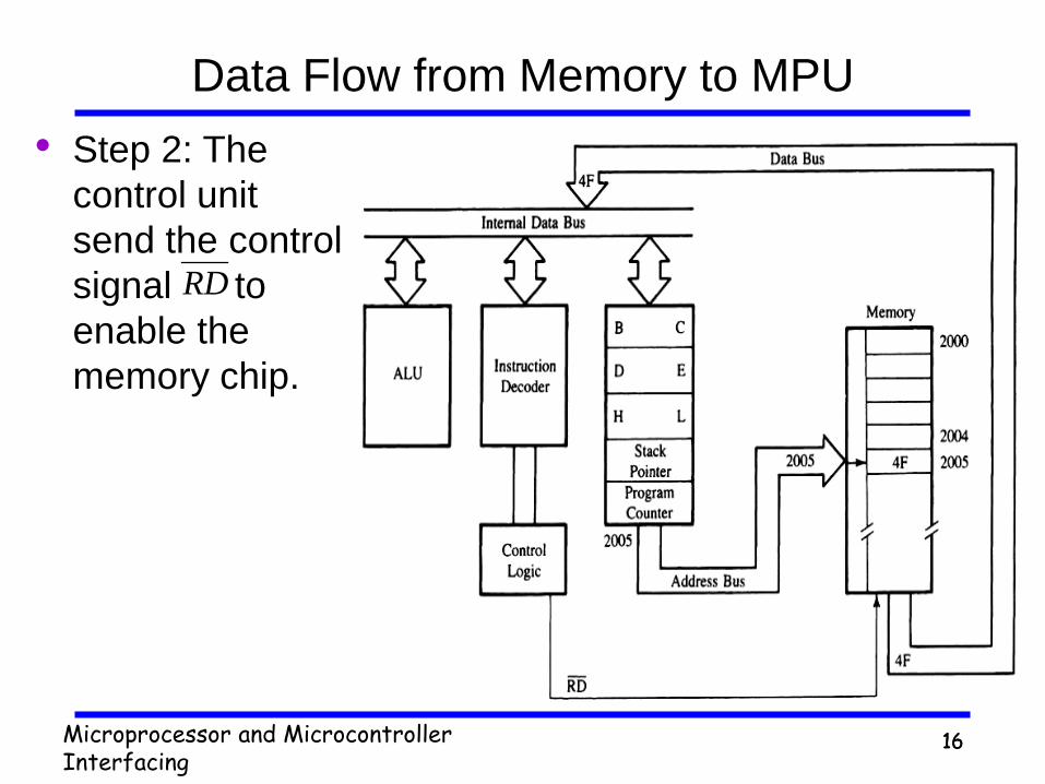
Data Flow from Memory to MPU
Microprocessor and Microcontroller Interfacing
1616
• Step 2: The
control unit
send the control
signal to
enable the
memory chip.
RD
Data Flow from Memory to MPU
Microprocessor and Microcontroller Interfacing
1717
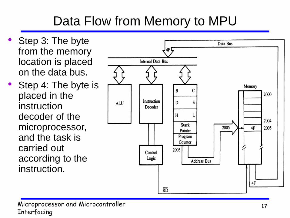
Data Flow from Memory to MPU
• Step 3: The byte from the memory location is placed on the data bus.
• Step 4: The byte is placed in the instruction decoder of the microprocessor, and the task is carried out according to the instruction.

Microprocessor and Microcontroller Interfacing
1818
Timing Diagram for Opcode Fetch (mov C,A)
Microprocessor and Microcontroller Interfacing
19
Instruction cycle, Machine cycle & T-state
• Instruction Cycle:
– It is defined as the time required to complete the execution
of an instruction.
– The 8085 instruction cycle consists of one to six machine
cycles or operations.
• Machine Cycle:
– It is defined as the time required to complete one operation
of accessing memory, I/O, or acknowledging an external
request.
– This may consist of three to six T-states (cycles).
• T-state:
– It is defined as one subdivision of operation performed in
one clock period.
– Generally it is equal to one clock cycle.
Microprocessor and Microcontroller Interfacing
20
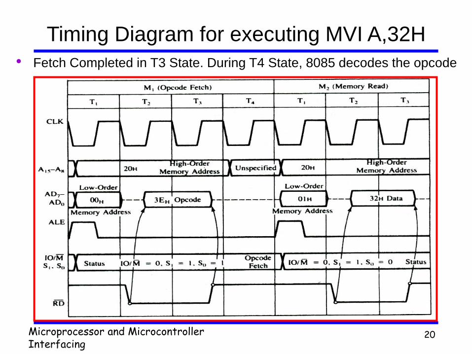
Timing Diagram for executing MVI A,32H
• Fetch Completed in T3 State. During T4 State, 8085 decodes the opcode
Microprocessor and Microcontroller Interfacing
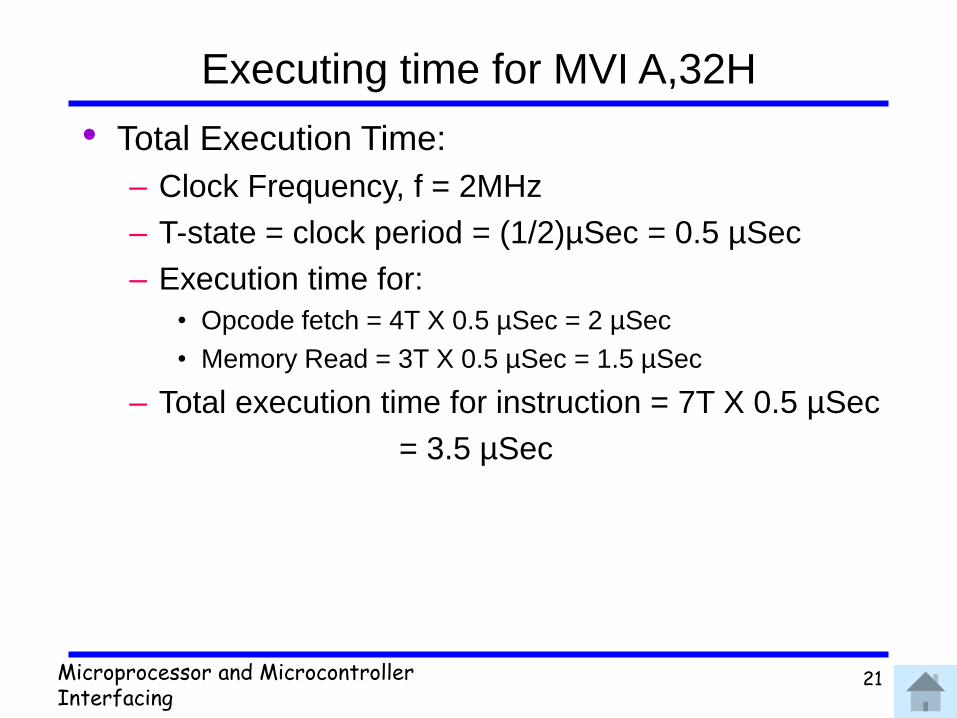
21
• Total Execution Time:
– Clock Frequency, f = 2MHz
– T-state = clock period = (1/2)µSec = 0.5 µSec
– Execution time for:
• Opcode fetch = 4T X 0.5 µSec = 2 µSec
• Memory Read = 3T X 0.5 µSec = 1.5 µSec
– Total execution time for instruction = 7T X 0.5 µSec
= 3.5 µSec
Executing time for MVI A,32H
Microprocessor and Microcontroller Interfacing
22
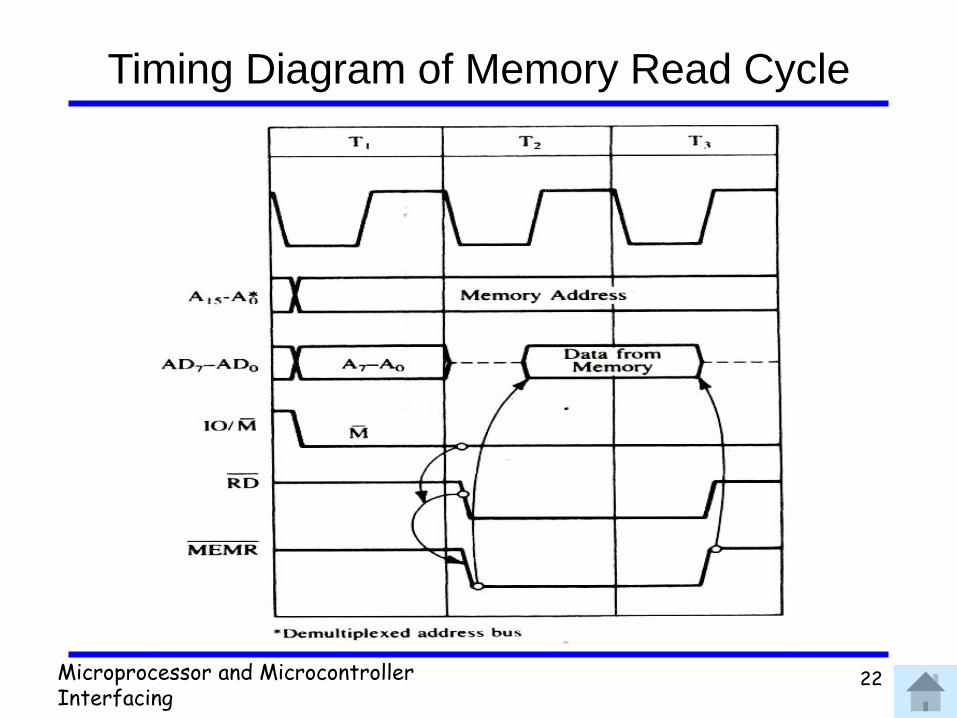
Timing Diagram of Memory Read Cycle

Microprocessor and Microcontroller Interfacing
23
Timing Diagram of Memory Write Cycle
Microprocessor and Microcontroller Interfacing
24
Thank you
Any Quarries?
Related Documents