Approved by Electronics Sequence Committee on Feb 7, 2011. Page 1 UMM AL-QURA UNIVERSITY Department of Electrical Engineering D D I I G G I I T T A A L L E E L L E E C C T T R R O O N N I I C C S S ( 8 8 0 0 2 2 4 4 1 1 2 2 - - 4 4 ) ) Laboratory Manual Prepared By Dr. Mohammed Jameel Alawi

802412-4 Digital Electronics Lab Manual
Oct 24, 2015
sfg
Welcome message from author
This document is posted to help you gain knowledge. Please leave a comment to let me know what you think about it! Share it to your friends and learn new things together.
Transcript
Approved by Electronics Sequence Committee on Feb 7, 2011. Page 1
UMM AL-QURA UNIVERSITY Department of Electrical Engineering
DDIIGGIITTAALL EELLEECCTTRROONNIICCSS
(880022441122--44))
Laboratory Manual
Prepared By
Dr. Mohammed Jameel Alawi

Approved by Electronics Sequence Committee on Feb 7, 2011. Page 2
Table of Contents Page
1. Introduction 3
2. Laboratory Safety 3
3. How to write a Lab Report 5
4. Experiment # 1: Diode-Resistor Logic (DRL) 7
5. Experiment # 2: The BJT Inverter(RTL) 10
6. Experiment # 3: Diode-Transistor Logic(DTL) 13
7. Experiment # 4: Modified DTL NAND Gates 15
8. Experiment # 5: Transistor-Transistor Logic (TTL) 20
9. Experiment # 6: TTL Design Project 23
10. Experiment # 7: Resistor-Loaded NMOS Inverter 25
11. Experiment # 8: CMOS Inverter 28
12. Experiment # 9: Emitter-Coupled Logic (ECL) 30
13. Experiment # 10: ECL Design Project 33
14. Experiment # 11: NMOS Inverter with saturated Enhancement Load 36
Approved by Electronics Sequence Committee on Feb 7, 2011. Page 3
1. INTRODUCTION
The objective of this lab is to make the students experimentally familiar with the operation of various digital circuits and logic families such as DL, BJT inverter, DTL, TTL ECL and NMOS. Also, the student will be able to analyze them experimentally. In most of the experiments, the emphasis will be on how to obtain the voltage-transfer characteristic and critical voltages for the digital circuits. References: T. A. DeMassa and Z. Ciccone,”Digital Integrated Circuit,” John Wiley & Sons, 1996. Lab Instructions:
1- Preparation: Students should read, prepare, and understand the experiment before coming to lab.
2- Discipline: - Attendance on time in lab as scheduled is important.
- Each group in the lab is responsible for their bench condition (arrangement, cleaning, etc.) after finishing the experiment.
3- Reports: - The student is requested to submit a written formal report of the experiment in the next session.
- Any assignments of all experiments such as theoretical or simulated solution are the student responsibility.
Note: Through some lab assignments, you will be asked to simulate the experiment in specified steps using Spice analysis, available Electronic Work Bench 5. If possible you may get assistance to learn how to use it.
2. LABORATORY SAFETY
- Safety in the electrical engineering laboratory, as everywhere else, is a matter of the
knowledge of potential hazards, following safety regulations and precautions, and
common sense.
- Observing safety precautions is important due to pronounced hazards in any electrical
engineering laboratory.
- All the UQU Electrical Engineering Students, Teaching Assistants, Lab Engineers, and
Lab technicians are required to be familiar with the LABORATORY SAFETY
GUIDELINES FOR THE UQU ELECTRICAL ENGINEERING UNDERGRADUATE
LAB AREAS published on the department web-page.
- Practice electrical safety at all times while constructing, analyzing and troubleshooting
circuitry.
Approved by Electronics Sequence Committee on Feb 7, 2011. Page 4
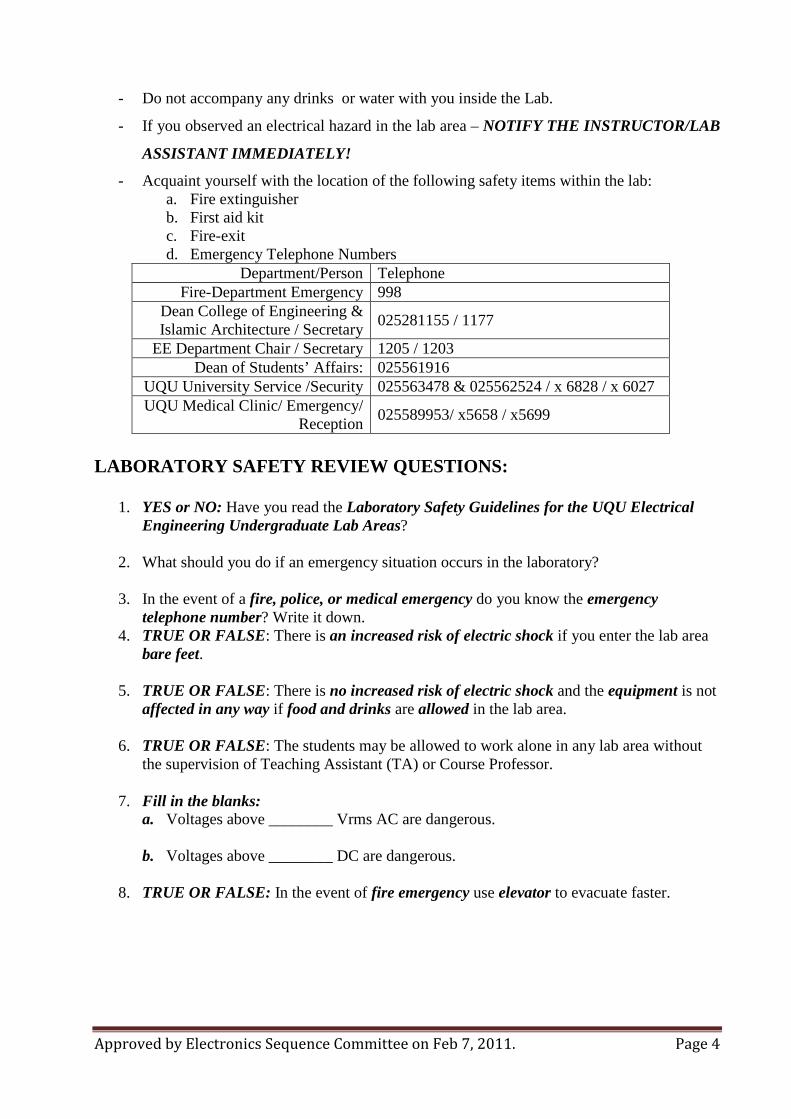
- Do not accompany any drinks or water with you inside the Lab.
- If you observed an electrical hazard in the lab area – NOTIFY THE INSTRUCTOR/LAB
ASSISTANT IMMEDIATELY!
- Acquaint yourself with the location of the following safety items within the lab: a. Fire extinguisher b. First aid kit c. Fire-exit d. Emergency Telephone Numbers
Department/Person Telephone Fire-Department Emergency 998
Dean College of Engineering & Islamic Architecture / Secretary 025281155 / 1177
EE Department Chair / Secretary 1205 / 1203 Dean of Students’ Affairs: 025561916
UQU University Service /Security 025563478 & 025562524 / x 6828 / x 6027 UQU Medical Clinic/ Emergency/
Reception 025589953/ x5658 / x5699
LABORATORY SAFETY REVIEW QUESTIONS:
1. YES or NO: Have you read the Laboratory Safety Guidelines for the UQU Electrical Engineering Undergraduate Lab Areas?
2. What should you do if an emergency situation occurs in the laboratory?
3. In the event of a fire, police, or medical emergency do you know the emergency telephone number? Write it down.
4. TRUE OR FALSE: There is an increased risk of electric shock if you enter the lab area bare feet.
5. TRUE OR FALSE: There is no increased risk of electric shock and the equipment is not affected in any way if food and drinks are allowed in the lab area.
6. TRUE OR FALSE: The students may be allowed to work alone in any lab area without the supervision of Teaching Assistant (TA) or Course Professor.
7. Fill in the blanks: a. Voltages above ________ Vrms AC are dangerous.
b. Voltages above ________ DC are dangerous.
8. TRUE OR FALSE: In the event of fire emergency use elevator to evacuate faster.
Approved by Electronics Sequence Committee on Feb 7, 2011. Page 5
3. HOW TO WRITE A LAB REPORT
A lab report for each experiment is to be submitted by each member (student) of a team one week after the lab session is completed. The lab report must be type written in the MSWord (Times-Roman 12 font) format and it must contain the following:
1. Cover page containing:
• Digital Electronics Lab: 802312-4
• Experiment #______
• Experiment Title: _________________________________
• Group #: ___________
• Your Name: ________________ & I.D. #: _________________
2. Objectives: Not copied from the lab manual
3. Specifications of Equipment Used:
4. Block Diagram or Circuit Diagram should be included
5. Formulae / Design if any, is to be given.
6. Procedure: Steps you did in the lab. It is not copied from the lab manual
7. Result or Analysis: Compare the Pre-lab results with those obtained in the experiment.
Summary of what you discovered. (attach the pre-lab with the lab report)
8. Answers to Questions: Answer to observation questions in the lab experiment, lab review questions and lab safety review questions at the end of the experiment in a written form (MSWord document)
9. Conclusion: The conclusions based on the experiment and other observations must be clearly discussed in the laboratory report.
10. Remarks or Comments: You may write your comments regarding your experience of each lab experiment.
(The laboratory report will be graded for content and written English

Approved by Electronics Sequence Committee on Feb 7, 2011. Page 6
802412-4-DIGITAL ELECTRONICS
EXPERIMENT # 1: DIODE-RESISTOR LOGIC (DRL) OBJECTIVES:
I. To study the AND & OR gates Constructed by using the Diode Logic (DL).
II. To construct a wired-logic OR gate and verify its operation. EQUIPMENTS:
Power supply, digital multimeter, diodes (1N4007) and resistors. BACKGROUND:
In the first part of this experiment positive-logic AND, OR gates will be constructed using
diode logic. That is, logic 0 state will be requested as LOW, while logic 1 state will correspond to HIGH.
(a)
(b)
Figure 1 : Wired-Logic OR gate .
To explain the concept of wired-logic, consider the Boolean function F (w,x,y,z) = w+x+y+z, implemented by two-input OR gates as shown in Figure 1 (a). Considering that each OR gate is constructed by using diode logic, as in part I of this experiment, it can be shown that the OR gate 3 is redundant, and the outputs of OR gates 1 and 2 can be directly wired together, as shown in Figure 1 (b), without affecting the implementation of the above function F. This is known as wired-logic.
Approved by Electronics Sequence Committee on Feb 7, 2011. Page 7
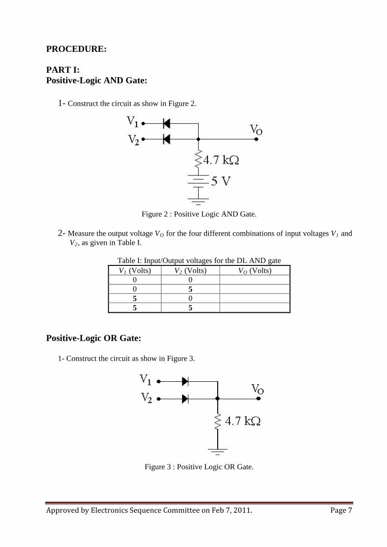
PROCEDURE: PART I: Positive-Logic AND Gate:
1- Construct the circuit as show in Figure 2.
Figure 2 : Positive Logic AND Gate.
2- Measure the output voltage VO for the four different combinations of input voltages V1 and V2
V
, as given in Table I.
Table I: Input/Output voltages for the DL AND gate 1 V (Volts) 2 V (Volts) O (Volts)
0 0 0 5 5 0 5 5
Positive-Logic OR Gate:
1- Construct the circuit as show in Figure 3.
Figure 3 : Positive Logic OR Gate.

Approved by Electronics Sequence Committee on Feb 7, 2011. Page 8
2- Measure the output voltage VO for the four different combinations of input voltages V1 and V2
V
, as given in Table II.
Table II: Input/Output voltages for the DL OR gate. 1 V (Volts) 2 V (Volts) O (Volts)
0 0 0 5 5 0 5 5
PART II: Wired Logic
1- Construct the circuit as show in Figure 4.
Figure 4 : Wired- Logic OR Gate.
2- Measure the output voltage VO
V
for different values input voltages and fill Table III with the measured values.
Table III: Wired-Logic OR gate
1 V (Volts) 2 V (Volts) 3 V (Volts) 4 V (Volts) O (Volts) 0 0 0 0 0 0 0 5 0 0 5 0 0 5 0 0 5 0 0 0 5 0 5 0 5 5 5 5
Instructor’s Signature Date
Approved by Electronics Sequence Committee on Feb 7, 2011. Page 9
DISCUSSION:
1- On the basis of your results obtained in Table I, show that the circuit of Figure 2 behaves as AND gate for positive logic, but it will function as an OR gate for negative logic. Similarly, show that the results of Table II indicate the circuit of Figure 3 behaves as an OR gate for positive logic and as an AND for negative logic.
2- Explain why the measured values of output voltage in Table I and II are different from those obtained by using “ideal” diodes.
3- Using your results in Table I and II, calculate the power dissipation in the AND & OR gates implemented in circuits of Figure 2 and 3, respectively. Explain your procedure.
PRE-LAB:
The following pre-lab must be completed and submitted before the start of this experiment. The pre-lab shall be graded and is part of your lab grades.
Solve the following exercises on separate sheets of paper and submit your solution before the start of the lab experiment.
1- Verify theoretically that circuit of Figure 4 is in fact a 4-input OR gate.
2- Draw a wired-logic AND gate to implement the function:
F (w, x, y, z) = w.x.y.z
Approved by Electronics Sequence Committee on Feb 7, 2011. Page 10
802-412-4- DIGITAL ELECTRONICS
EXPERIMENT # 2: THE BJT INVERTER (RTL) OBJECTIVES:
(i) To draw the transfer characteristics of the BJT inverter and to determine its noise margins.
(ii) To observe and to determine (approximately) the propagation delay times.
EQUIPMENT:
Power supply, function generator, oscilloscope, digital multimeter, potentiometer, resistors and BJT transistor (BCY 58 or BC 550).
BACKGROUND:
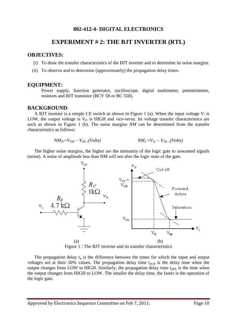
A BJT inverter is a simple CE switch as shown in Figure 1 (a). When the input voltage Vi is LOW, the output voltage is VO is HIGH and vice-versa. Its voltage transfer characteristics are such as shown in Figure 1 (b). The noise margins NM can be determined from the transfer characteristics as follows:
NMH=VOH – VIH ,(Volts) NML=VIL – VOL ,(Volts)
The higher noise margins, the higher are the immunity of the logic gate to unwanted signals (noise). A noise of amplitude less than NM will not alter the logic state of the gate.
(a) (b)
Figure 1 : The BJT inverter and its transfer characteristics
The propagation delay tp is the difference between the times for which the input and output voltages are at their 50% values. The propagation delay time tpLH is the delay time when the output changes from LOW to HIGH. Similarly, the propagation delay time tpHL is the time when the output changes from HIGH to LOW. The smaller the delay time, the faster is the operation of the logic gate.
Approved by Electronics Sequence Committee on Feb 7, 2011. Page 11
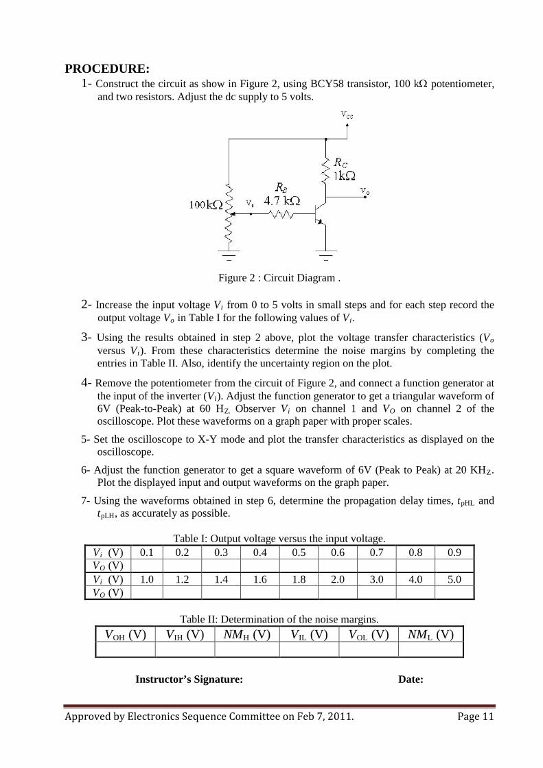
PROCEDURE: 1- Construct the circuit as show in Figure 2, using BCY58 transistor, 100 kΩ potentiometer,
and two resistors. Adjust the dc supply to 5 volts.
Figure 2 : Circuit Diagram .
2- Increase the input voltage Vi from 0 to 5 volts in small steps and for each step record the output voltage Vo in Table I for the following values of Vi.
3- Using the results obtained in step 2 above, plot the voltage transfer characteristics (Vo versus Vi). From these characteristics determine the noise margins by completing the entries in Table II. Also, identify the uncertainty region on the plot.
4- Remove the potentiometer from the circuit of Figure 2, and connect a function generator at the input of the inverter (Vi). Adjust the function generator to get a triangular waveform of 6V (Peak-to-Peak) at 60 HZ. Observer Vi on channel 1 and VO on channel 2 of the oscilloscope. Plot these waveforms on a graph paper with proper scales.
5- Set the oscilloscope to X-Y mode and plot the transfer characteristics as displayed on the oscilloscope.
6- Adjust the function generator to get a square waveform of 6V (Peak to Peak) at 20 KHZ. Plot the displayed input and output waveforms on the graph paper.
7- Using the waveforms obtained in step 6, determine the propagation delay times, tpHL and tpLH
V
, as accurately as possible.
Table I: Output voltage versus the input voltage. i 0.1 (V) 0.2 0.3 0.4 0.5 0.6 0.7 0.8 0.9
VO (V) Vi 1.0 (V) 1.2 1.4 1.6 1.8 2.0 3.0 4.0 5.0 VO (V)
Table II: Determination of the noise margins. VOH V (V) IH NM (V) H V (V) IL V (V) OL NM (V) L (V)
Instructor’s Signature: Date:
Approved by Electronics Sequence Committee on Feb 7, 2011. Page 12
DISCUSSION:
1- Give your detailed comments about the results obtained in this experiment.
2- Are the noise margins of this inverter appropriate for general-purpose applications?
3- Which delay time is greater than the other, and why?
4- How you improve the switching speed of this inverter? Explain in detail.
PRE-LAB:
The following pre-lab must be completed and submitted before the start of this experiment. The pre-lab shall be graded and is part of your lab grades.
Solve the following exercises on separate sheets of paper and submit your solution before the start of the lab experiment.
1. Analyze the circuit of Fig.1 2. Simulate circuit of Fig. 1, using PSPICE.

Approved by Electronics Sequence Committee on Feb 7, 2011. Page 13
802-412-4- DIGITAL ELECTRONICS
EXPERIMENT # 3: DIODE-TRANSISTOR LOGIC (DTL) OBJECTIVES:
To understand the function of a simplified DTL NAND gate. EQUIPMENTS:
Power supply, digital multimeter, resistors, transistor (BCY 58 or BC 550), diodes (1N4007).
BACKGROUND:
The simplified DTL NAND gate constructed in this experiment is basically developed from the diode logic AND gate and the BJT inverter.
PROCEDURE:
1- Construct the circuit as shown in Figure 1.
Figure 1 : Simplified DTL NAND gate.
2- Apply different input voltages as given in Table I and measure the output voltage VO. 3- Replace diode D2
V
with a short-circuit and once again measure the output voltage for each combination of the input voltages as given in Table I.
Table I: DTL NAND gate results
A V (Volts) BV (Volts) O (Volts) (with D2
V)
O (Volts) (without D2)
0 0 0 5 5 0 5 5
Instructor’s Signature: Date:
Approved by Electronics Sequence Committee on Feb 7, 2011. Page 14
DISCUSSION:
1- Explain the operation of the circuit shown in Figure 1.
2- When do you really need to put diode D2
3- From your results obtained in Table I, verify that the circuit functions as a NAND gate.
in the circuit?
PRE-LAB:
The following pre-lab must be completed and submitted before the start of this experiment. The pre-lab shall be graded and is part of your lab grades.
Solve the following exercises on separate sheets of paper and submit your solution before the start of the lab experiment.
1. Analyze the circuit of Fig.1 2. Simulate circuit of Fig. 1, using PSPICE.
Approved by Electronics Sequence Committee on Feb 7, 2011. Page 15
802-412-4- DIGITAL ELECTRONICS
EXPERIMENT # 4: MODIFIED DTL NAND GATES OBJECTIVES:
I. To investigate the operation of the circuit and to calculate its noise margins.
II. Determine the fanout of the circuit and compare it with the theoretical values.
EQUIPMENT:
Power supply digital multimeter, potentiometer (100 kΩ), transistors (BC550), diodes (1N4007), and resistors.
BACKGROUND:
In Experiment 3, a simple DTL NAND gate was studied. That circuit is modified be replacing the diode D1 with a transistor T1 so that there is an increase in the base current of the output transistor without a corresponding increase in the current load imposed by each additional gate. Thus, the fanout of the gate is considerably increased. This circuit is shown in Figure1. PROCEDURES:
1- Construct the circuit as shown in Figure 1. Adjust the dc supply to 5 volts.
Figure 1 : Modified DTL NAND gate .
2- Measure the output voltage for each set of input voltages as given in Table I.
3- Set VB to 5 volts (Logic ‘1’).

Approved by Electronics Sequence Committee on Feb 7, 2011. Page 16
Table I: Input/Output Relationship VA V (Volts) B V (Volts) O (Volts)
0 0 0 5 5 0 5 5
4- Connect the 100 kΩ potentiometer to input VA as shown in the Figure 2. Increase the input
voltage VA form 0 to 5 volts in small steps and for each step record the output voltage VO in Table II.
Note: You may need to record some additional readings around the cut-in voltage.
Figure 2 : Circuit for input VA trough potentiometer.
Table II: Output voltage VO versus input voltage VA for VB
V set to logic '1'
A 0.1 (V) 0.2 0.3 0.4 0.5 0.6 0.7 0.8 0.9 1.0 VO (V) VA 1.2 (V) 1.4 1.6 1.8 2.0 2.2 2.6 3.0 4.0 5.0 VO (V)
5- Using the results obtained in step 4 above, plot the voltage transfer characteristics (VO versus VA
V
). From these characteristics determine the noise margins by completing the entries in Table III.
Table III: Determination of the noise margins for the Modified DTL gate. OH V (V) IH NM (V) H V (V) IL V (V) OL NM (V) L (V)
6- Remove the potentiometer from the circuit of figure 2. Connect VA to ground logic‘0’ through an ammeter. Measure the current passing through diode DA.
IDA = ____________________
Approved by Electronics Sequence Committee on Feb 7, 2011. Page 17
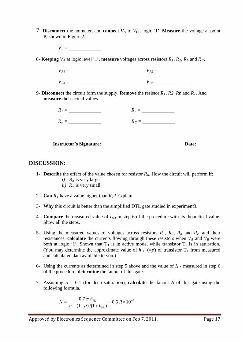
7- Disconnect the ammeter, and connect VA to VCC logic ‘1’. Measure the voltage at point P, shown in Figure 2.
VP = ____________________
8- Keeping VA at logic level ‘1’, measure voltages across resistors R1, R2, Rb and RC.
VR1 = ____________________ VR2 = ____________________
VRb = ____________________ VRc = ____________________
9- Disconnect the circuit form the supply. Remove the resistor R1, R2, Rb and Rc. And measure their actual values.
R1 = ____________________ R2 = ____________________
Rb = ____________________ RC =
1- Describe the effect of the value chosen for resistor R
____________________
Instructor’s Signature: Date: DISCUSSION:
bi) R
. How the circuit will perform if: b
ii) R is very large,
b
2- Can R
is very small.
1 have a value higher than R2
3- Why this circuit is better than the simplified DTL gate studied in experiment3.
? Explain.
4- Compare the measured value of IDA
5- Using the measured values of voltages across resistors R
in step 6 of the procedure with its theoretical value. Show all the steps.
1, R2, Rb and Rc, and their resistances, calculate the currents flowing through these resistors when VA and VB were both at logic ‘1’. Shown that T1 is in active mode, while transistor T2 is in saturation. (You may determine the approximate value of hFE (=β) of transistor T1
6- Using the currents as determined in step 5 above and the value of I
from measured and calculated data available to you.)
DA
7- Assuming σ = 0.1 (for deep saturation), calculate the fanout N of this gate using the following formula,
measured in step 6 of the procedure, determine the fanout of this gate.
3
FE
FE 10 6.0)1/()-(1
7.0 −×−++
= Rh
hNρρσ

Approved by Electronics Sequence Committee on Feb 7, 2011. Page 18
8- Compare the experimentally determined fanout value of step 6 with the theoretically calculated value of step 7. Explain the difference, if any.
9- For VA and VB
PRE-LAB:
The following pre-lab must be completed and submitted before the start of this experiment. The pre-lab shall be graded and is part of your lab grades.
Solve the following exercises on separate sheets of paper and submit your solution before the start of the lab experiment.
both set logic ‘1’, determine the power dissipated in the gate using the measured values.
1. Analyze the circuit of Fig.1 2. Simulate circuit of Fig. 1, using PSPICE.
Approved by Electronics Sequence Committee on Feb 7, 2011. Page 19
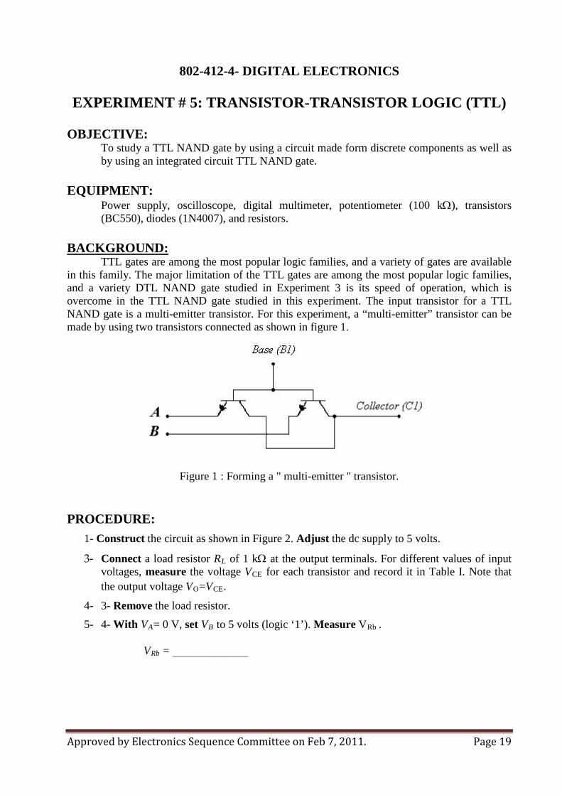
802-412-4- DIGITAL ELECTRONICS
EXPERIMENT # 5: TRANSISTOR-TRANSISTOR LOGIC (TTL) OBJECTIVE:
To study a TTL NAND gate by using a circuit made form discrete components as well as by using an integrated circuit TTL NAND gate.
EQUIPMENT:
Power supply, oscilloscope, digital multimeter, potentiometer (100 kΩ), transistors (BC550), diodes (1N4007), and resistors.
BACKGROUND:
TTL gates are among the most popular logic families, and a variety of gates are available in this family. The major limitation of the TTL gates are among the most popular logic families, and a variety DTL NAND gate studied in Experiment 3 is its speed of operation, which is overcome in the TTL NAND gate studied in this experiment. The input transistor for a TTL NAND gate is a multi-emitter transistor. For this experiment, a “multi-emitter” transistor can be made by using two transistors connected as shown in figure 1.
Figure 1 : Forming a " multi-emitter " transistor.
PROCEDURE:
1- Construct the circuit as shown in Figure 2. Adjust the dc supply to 5 volts.
3- Connect a load resistor RL of 1 kΩ at the output terminals. For different values of input voltages, measure the voltage VCE for each transistor and record it in Table I. Note that the output voltage VO=VCE
4- 3- Remove the load resistor.
.
5- 4- With VA= 0 V, set VB to 5 volts (logic ‘1’). Measure VRb
V
.
Rb = ____________________
Approved by Electronics Sequence Committee on Feb 7, 2011. Page 20
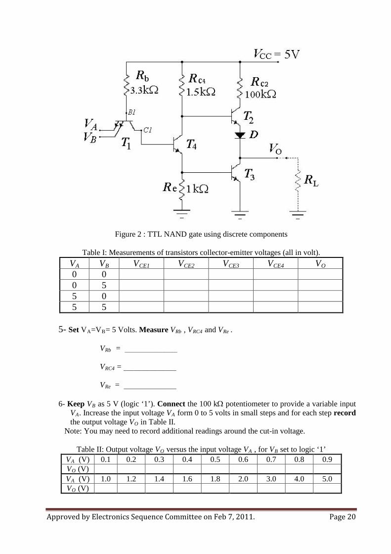
Figure 2 : TTL NAND gate using discrete components
Table I: Measurements of transistors collector-emitter voltages (all in volt). V VA VB VCE1 VCE2 VCE3 VCE4 O 0 0 0 5 5 0 5 5
5- Set VA=VB= 5 Volts. Measure VRb , VRC4 and VRe .
VRb = ____________________
VRC4 = ____________________
VRe = ____________________
6- Keep VB as 5 V (logic ‘1’). Connect the 100 kΩ potentiometer to provide a variable input VA. Increase the input voltage VA form 0 to 5 volts in small steps and for each step record the output voltage VO in Table II.
Note: You may need to record additional readings around the cut-in voltage.
Table II: Output voltage VO versus the input voltage VA , for VB
V set to logic ‘1’
A 0.1 (V) 0.2 0.3 0.4 0.5 0.6 0.7 0.8 0.9 VO (V) VA 1.0 (V) 1.2 1.4 1.6 1.8 2.0 3.0 4.0 5.0 VO (V)

Approved by Electronics Sequence Committee on Feb 7, 2011. Page 21
7- Using the results obtained in step 6 above, plot the voltage transfer characteristics (VO versus VA
V
). From these characteristics determine the noise margins by completing the entries in Table III.
Table III: Determination of the noise margins for the TTL NAND gate. OH V (V) IH NM (V) H V (V) IL V (V) OL NM (V) L (V)
8- Remove the potentiometer. Keeping input VB as HIGH, apply a square wave of 10Vp-p (100HZ) at input VA. Observe the output voltage VO on the oscilloscope and plot both input and output voltages on a graph paper. Repeat this with capacitive loads of 0.47µF and 4.7µF.
9- Disconnect the circuit and measure the resistance of the entire resistor. Record their values.
10- Using a single gate of the TTL 7400 chip (Quadruple 2-input NAND gates), as shown in Figure 3, repeat step 6 and 7.
Figure 3 : TTL Chip 7400
Instructor’s Signature: Date: DISCUSSION:
1- On the basis of measured voltages in Table I, determine the mode of operation of each transistor for various combinations of input voltages.
2- Using the voltages measured in step 4 and step 5, and the measured values of resistors, calculate various currents to determine the fanout of the gate. Mention any assumptions you need to make.
3- Comment on the results obtained in step 8 above.
4- How the output waveforms will look different form those obtained in step 8, if the active pull-up in the circuit was replaced by a passive pull-resistor. Explain.
5- Comment on the transfer characteristics of the 7400 gate as determined in step 10 above.
Approved by Electronics Sequence Committee on Feb 7, 2011. Page 22
PRE-LAB:
The following pre-lab must be completed and submitted before the start of this experiment. The pre-lab shall be graded and is part of your lab grades.
Solve the following exercises on separate sheets of paper and submit your solution before the start of the lab experiment.
1. Analyze the circuit of Fig.2 2. Simulate circuit of Fig. 2, using PSPICE.

Approved by Electronics Sequence Committee on Feb 7, 2011. Page 23
802-412-4- DIGITAL ELECTRONICS
EXPERIMENT # 6: TTL DESIGN PROJECT OBJECTIVES:
To design and test a TTL NOR gate by using a circuit made from discrete components. EQUIPMENTS:
Power supply, function generator, oscilloscope, digital multimeter, diodes (1N4007), transistors (BC550), potentiometer (100 kΩ), and resistors.
PROCEDURE
1- Construct the circuit as shown in Figure 1. Adjust the dc supply to 5 volts.
Figure 1 : TTL NOR .
2- For different values of input voltages, measure the output voltage VO for circuit and record it in Table I.
3- Set VB = 0 (logic '0'). Connect the 100 kΩ potentiometer VA form 0 to 5 volts in small steps & for each step record the output voltage VO
Table I: Input/Output voltages.
in Table II.
VA V (Volts) B V (Volts) O (Volts) 0 0 0 5 5 0 5 5

Approved by Electronics Sequence Committee on Feb 7, 2011. Page 24
Table II: Output voltage VO versus the input voltage VA for VB
V set to logic ‘0’
A 0.1 (V) 0.2 0.3 0.4 0.5 0.6 0.7 0.8 0.9 VO (V) VA 1.0 (V) 1.2 1.4 1.6 1.8 2.0 3.0 4.0 5.0 VO (V)
4- Using results obtained in step 3 above, plot the voltage transfer characteristics (VO versus VA
V
). Determine the noise margins by completing Table III.
Table III: Determination of the noise margins for the TTL NOR gate. OH V (V) IH NM (V) H V (V) IL V (V) OL NM (V) L (V)
5- Remove the potentiometer and use two-function generators, one for VA & other one for VB. Apply a square-wave of 10 Vp-p (1kHz) at VA and a square-wave of 10 Vp-p (2kHz) at input VB.
6- Observe the output VO and plot both inputs voltages & the output voltage on a graph paper.
Instructor’s Signature: Date: DISCUSSION:
1- Theoretically, calculate the output voltage for different states of inputs and plot the voltage-transfer characteristics. Compare it with the experimental results.
2- Repeat steps 5 & 6, using SPICE analysis (such as Electronic-Work-Bench 5 or Orcad 9).
3- Plot the voltage-transfer characteristics using the SPICE analysis.
PRE-LAB:
The following pre-lab must be completed and submitted before the start of this experiment. The pre-lab shall be graded and is part of your lab grades.
Solve the following exercises on separate sheets of paper and submit your solution before the start of the lab experiment.
1. Analyze the circuit of Fig.1 2. Simulate circuit of Fig. 1, using PSPICE.

Approved by Electronics Sequence Committee on Feb 7, 2011. Page 25
802-412-4- DIGITAL ELECTRONICS
EXPERIMENT # 7: RESISTOR-LOADED NMOS INVERTER OBJECTIVES:
I. To determine the values of parameters ‘k’ and ‘VT’ of the given NMOS and plot its output characteristics.
II. To plot the voltage transfer characteristics of the NMOS inverter with resistive load and determine the noise margins.
EQUIPMENT:
Power supply, digital multimeter, potentiometer, N-MOSFET (BS170) and resistors. BACKGROUND: The current ID for NMOS is given as,
1- Ohmic (Linear) Region: (VDS ≤ VGS - VT)
ID = k [2 (VGS - VT) VDS – VDS2]
2 – Saturation Region: (VDS ≥ VGS - VT)
ID = k [(VGS - VT) 2]
Once the values of parameters k and VT are known, the output characteristics of NMOS can be plotted. (You may use a computer program for plotting)
PROCEDURE:
1- Connect the circuit as shown in the Figure 1. Note that for this connections VDS = VGS and the NMOS will be in the saturation mode.
2- For different values of the variable resistor RV measure VDS and ID. Record these values in Table I.
Figure 1 : Circuit for determining NMOS parameter.
Approved by Electronics Sequence Committee on Feb 7, 2011. Page 26
Table I: Measured values of drain current and drain-to-source voltage. ID (µA) VDS (V) ID (µA) VDS (V)
3- Plot DI versus VGS (=VDS).
4- Find VT form the intersection of the resulting straight line and VGS axis. The equation of this straight line is,
DI = k [(VGS - VT)]
5- From the slope of the straight line obtained in step 3, determine value of k.
6- Plot the output characteristics ID versus VDS using the data in Table I. Identify the ohmic and saturation region.
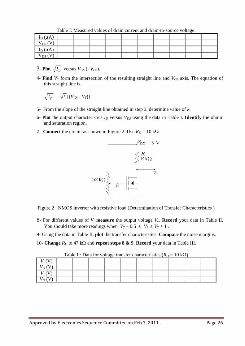
7- Connect the circuit as shown in Figure 2. Use RD = 10 kΩ.
Figure 2 : NMOS inverter with resistive load (Determination of Transfer Characteristics )
8- For different values of Vi measure the output voltage Vo. Record your data in Table II. You should take more readings when VT – 0.5 ≤ Vi ≤ VT + 1 .
9- Using the data in Table II, plot the transfer characteristics. Compare the noise margins.
10- Change RD to 47 kΩ and repeat steps 8 & 9. Record your data in Table III.
Table II: Data for voltage transfer characteristics (RD = 10 kΩ) Vi (V) VO (V) Vi (V) VO (V)
Approved by Electronics Sequence Committee on Feb 7, 2011. Page 27
Table III: Data for voltage transfer characteristics (RD = 47 kΩ) Vi (V) VO (V) Vi (V) VO (V)
Instructor’s Signature: Date: DISCUSSION:
1- Prove that the NMOS, as show in Figure 1, is in saturation mode.
2- Comment on the effect of different values of RD.
3- Mention one advantage and one disadvantage of using higher value of RD in the inverter circuit.
4- Why resistors are preferably replaced by MOSFETs in integrated circuits?
5- What have you learned after this experiment?
PRE-LAB:
The following pre-lab must be completed and submitted before the start of this experiment. The pre-lab shall be graded and is part of your lab grades.
Solve the following exercises on separate sheets of paper and submit your solution before the start of the lab experiment.
1. Analyze the circuit of Fig.2. 2. Simulate circuit of Fig. 2, using PSPICE.
Approved by Electronics Sequence Committee on Feb 7, 2011. Page 28
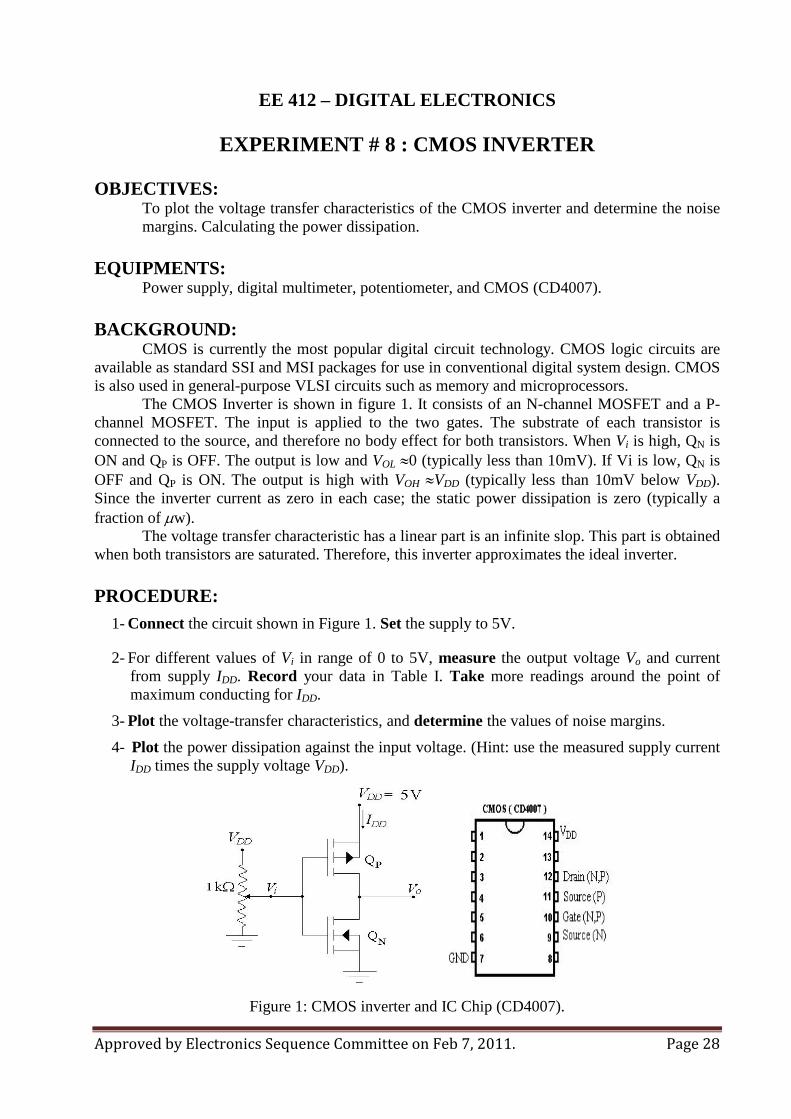
EE 412 – DIGITAL ELECTRONICS
EXPERIMENT # 8 : CMOS INVERTER OBJECTIVES:
To plot the voltage transfer characteristics of the CMOS inverter and determine the noise margins. Calculating the power dissipation.
EQUIPMENTS:
Power supply, digital multimeter, potentiometer, and CMOS (CD4007). BACKGROUND:
CMOS is currently the most popular digital circuit technology. CMOS logic circuits are available as standard SSI and MSI packages for use in conventional digital system design. CMOS is also used in general-purpose VLSI circuits such as memory and microprocessors.
The CMOS Inverter is shown in figure 1. It consists of an N-channel MOSFET and a P-channel MOSFET. The input is applied to the two gates. The substrate of each transistor is connected to the source, and therefore no body effect for both transistors. When Vi is high, QN is ON and QP is OFF. The output is low and VOL ≈0 (typically less than 10mV). If Vi is low, QN is OFF and QP is ON. The output is high with VOH ≈VDD (typically less than 10mV below VDD). Since the inverter current as zero in each case; the static power dissipation is zero (typically a fraction of µw).
The voltage transfer characteristic has a linear part is an infinite slop. This part is obtained when both transistors are saturated. Therefore, this inverter approximates the ideal inverter.
PROCEDURE:
1- Connect the circuit shown in Figure 1. Set the supply to 5V.
2- For different values of Vi in range of 0 to 5V, measure the output voltage Vo and current from supply IDD. Record your data in Table I. Take more readings around the point of maximum conducting for IDD.
3- Plot the voltage-transfer characteristics, and determine the values of noise margins.
4- Plot the power dissipation against the input voltage. (Hint: use the measured supply current IDD times the supply voltage VDD).
Figure 1: CMOS inverter and IC Chip (CD4007).

Approved by Electronics Sequence Committee on Feb 7, 2011. Page 29
Table I: Input / Output voltages and supply current measured for the CMOS inverter. Vi (V) 0 0.2 0.5 0.8 1.0 1.2 1.4 1.6 1.8 2.0 2.1 2.2 2.3 2.4 2.5 Vo (V)
IDD (mA) Vi(V) 2.6 2.7 2.8 2.9 3.0 3.1 3.2 3.4 3.6 3.8 4.0 4.2 4.5 4.8 5.0 Vo (V)
IDD (mA)
Instructor’s Signature: Date: DISCUSSION:
1- Compare the VTC of this inverter versus that of the NMOS inverters with saturated enhancement load as used in Experiment 10.
2- At which input and output voltage the power dissipation is maximum?
3- From your results, do you think that this CMOS Inverter is a Symmetric CMOS Inverter or not? Prove it.
4- On the VTC plot and the power dissipation plot, mention the mode of operation of each transistor (QP and QN).
PRE-LAB:
The following pre-lab must be completed and submitted before the start of this experiment. The pre-lab shall be graded and is part of your lab grades.
Solve the following exercises on separate sheets of paper and submit your solution before the start of the lab experiment.
1. Analyze the circuit of Fig.1. 2. Simulate circuit of Fig. 1, using PSPICE.
Approved by Electronics Sequence Committee on Feb 7, 2011. Page 30
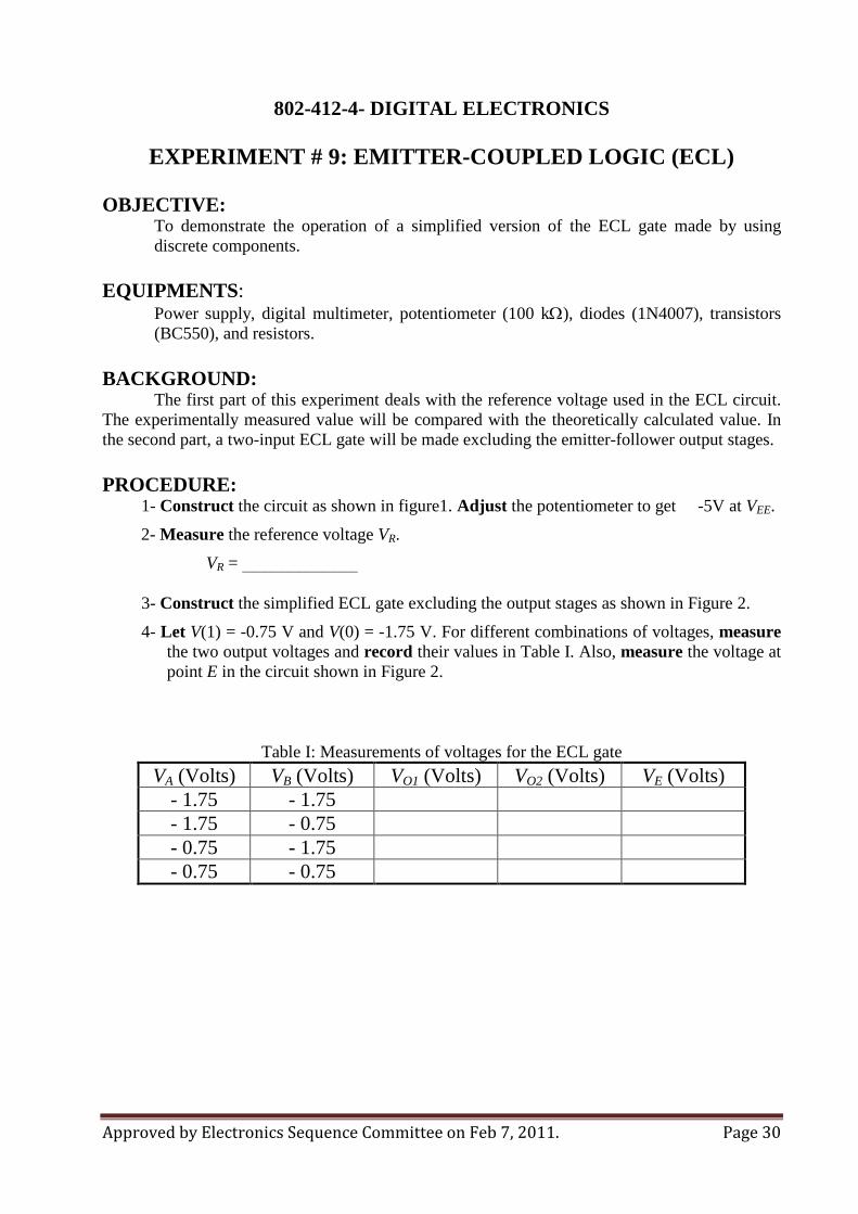
802-412-4- DIGITAL ELECTRONICS
EXPERIMENT # 9: EMITTER-COUPLED LOGIC (ECL) OBJECTIVE:
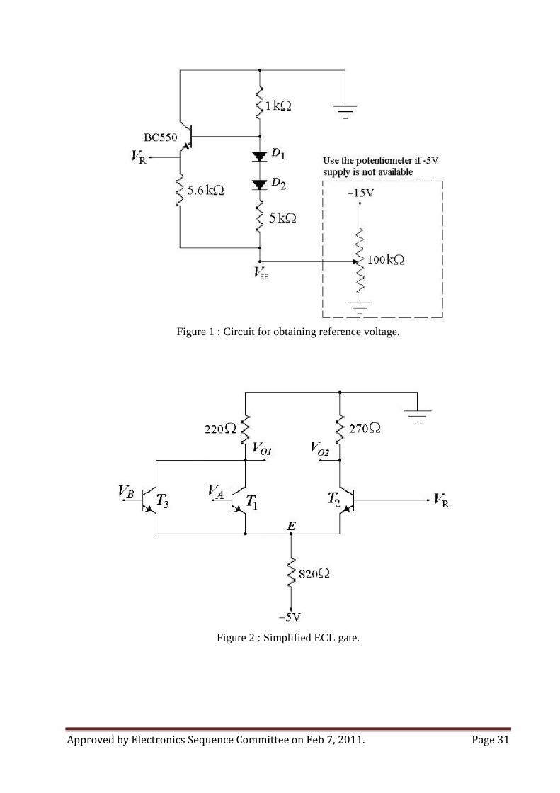
To demonstrate the operation of a simplified version of the ECL gate made by using discrete components.
EQUIPMENTS:
Power supply, digital multimeter, potentiometer (100 kΩ), diodes (1N4007), transistors (BC550), and resistors.
BACKGROUND:
The first part of this experiment deals with the reference voltage used in the ECL circuit. The experimentally measured value will be compared with the theoretically calculated value. In the second part, a two-input ECL gate will be made excluding the emitter-follower output stages. PROCEDURE:
1- Construct the circuit as shown in figure1. Adjust the potentiometer to get -5V at VEE.
2- Measure the reference voltage VR.
VR = ____________________
3- Construct the simplified ECL gate excluding the output stages as shown in Figure 2.
4- Let V(1) = -0.75 V and V(0) = -1.75 V. For different combinations of voltages, measure the two output voltages and record their values in Table I. Also, measure the voltage at point E in the circuit shown in Figure 2.
Table I: Measurements of voltages for the ECL gate VA (Volts) VB (Volts) VO1 (Volts) VO2 (Volts) VE (Volts)
- 1.75 - 1.75 - 1.75 - 0.75 - 0.75 - 1.75 - 0.75 - 0.75
Approved by Electronics Sequence Committee on Feb 7, 2011. Page 31
Figure 1 : Circuit for obtaining reference voltage.
Figure 2 : Simplified ECL gate.

Approved by Electronics Sequence Committee on Feb 7, 2011. Page 32
Table II : Output voltage VO2 versus the input voltage VA for VB set to logic '0' VA (V) 0.0 - 0.2 - 0.3 - 0.4 - 0.5 - 0.6 - 0.7 - 0.8 - 0.9 V02 (V) VA (V) - 1.0 - 1.1 - 1.2 - 1.3 - 1.4 - 1.5 - 1.6 - 1.8 - 2.0 V02 (V)
6- Using the results obtained in step 4 above , plot the voltage transfer characteristics (VO2 versus VA). From these characteristics determine the noise margins by completing the entries in Table III.
Table III: Determination of the noise margins for the ECL gate. VOH (V) VIH (V) NMH (V) VIL (V) VOL (V) NML (V)
7- Disconnect the circuit and measure the resistances of all the resistors used in the experiment. Record their values.
Instructor’s Signature: Date: DISCUSSION:
1- Compare the experimentally obtained value of reference voltage VR with the theoretically calculated value. Explain the difference between the two values.
2- On the basis of measured voltages in Table I, identify which output is for OR operation and which output is for NOR operation .
3- Using the measured voltages in Table I, determine the mode of operation of each transistor for various combinations of input voltages. Compare your results with theoretically expected modes of operation for these transistors.
4- Why the two levels of output voltage are not the same as the logic '0' and logic '1' voltages used in the experiment. Explain
PRE-LAB:
The following pre-lab must be completed and submitted before the start of this experiment. The pre-lab shall be graded and is part of your lab grades.
Solve the following exercises on separate sheets of paper and submit your solution before the start of the lab experiment.
1. Analyze the circuit of Fig.2 2. Simulate circuit of Fig. 2, using PSPICE.

Approved by Electronics Sequence Committee on Feb 7, 2011. Page 33
802-412-4- DIGITAL ELECTRONICS
EXPERIMENT # 10: ECL DESIGN PROJECT OBJECTIVES:
Design and test ECL AND gate, by using a circuit made from discrete components. EQUIPMENTS:
Function generator, power supply, digital multimeter, transistor (BC 550), diodes (1N4007), potentiometer (100 kΩ), and resistor.
SPECIFICATIONS:
• Logic swing: 800mV
• Power supply (VEE): 5.2 V
• Propagation delay: < 100nS (fanout=1)
PROCEDURE:
1- Construct the circuit as shown in Figure 1. Adjust the potentiometer to get -5.2V of -VEE. Measure the reference voltage VBB.
VBB = ____________________
2- Let V(1) = -0.75 V and V(0) = -1.75 V. for different combinations of input voltages, measure output VOUT. And record it in Table I.
Table I: Measurements of voltages. VA (Volts) VB (Volts) VOUT (Volts)
- 1.75 - 1.75 - 1.75 - 0.75 - 0.75 - 1.75 - 0.75 - 0.75
3- Set VB = V (1) = -0.75V. Using a potentiometer vary VA from 2 V to -2 V in small steps. Measure VOUT at each step and record it in Table II.
Table II: Output voltage VOUT versus the input voltage VA for VB set to logic '1'
VA (V) 0.0 - 0.2 - 0.3 - 0.4 - 0.5 - 0.6 - 0.7 - 0.8 - 0.9 V02 (V) VA (V) - 1.0 - 1.1 - 1.2 - 1.3 - 1.4 - 1.5 - 1.6 - 1.8 - 2.0 V02 (V)
4- Using these results obtained, plot voltage transfer characteristics (VOUT versus VA), and determine the noise margins by completing Table III.

Approved by Electronics Sequence Committee on Feb 7, 2011. Page 34
Figure 1 : ECL AND Gate

Approved by Electronics Sequence Committee on Feb 7, 2011. Page 35
Table III: Determination of the noise margins for the ECL gate. VOH (V) VIH (V) NMH (V) VIL (V) VOL (V) NML (V)
5- Remove the potentiometer, and use two function generators for VA and VB. Apply a square-wave of 1 Vp-p (1kHZ) with DC value -1 V at VA and a square-wave of 1 Vp-p (2kHZ) with DC value -1 V at VB.
6- Observe the output VOUT and plot both inputs & output waveforms on a graph paper.
Instructor’s Signature: Date: DISCUSSION:
1- Analyze the circuit theoretically. Obtain the output for different values of input and find the voltage-transfer characteristics. Compare it with the experimental results.
2- Repeat steps 5 & 6, using SPICE analysis (such as Electronic-Work-Bench 5 or Orcad 9).
3- Find the voltage-transfer characteristics using the SPICE analysis.
4- Comment on experimental results, theoretical results and SPICE results.
PRE-LAB:
The following pre-lab must be completed and submitted before the start of this experiment. The pre-lab shall be graded and is part of your lab grades.
Solve the following exercises on separate sheets of paper and submit your solution before the start of the lab experiment.
1. Analyze the circuit of Fig.1 2. Simulate circuit of Fig. 1, using PSPICE.

Approved by Electronics Sequence Committee on Feb 7, 2011. Page 36
802-412-4- DIGITAL ELECTRONICS
EXPERIMENT # 11: NMOS INVERTER WITH SATURATED ENHANCEMENT LOAD
OBJECTIVES:
To plot voltage transfer characteristics of the NMOS inverter with saturated enhancement load and determine the noise margins.
EQUIPMENTS:
Power supply, digital multimeter, potentiometer, and N-MOSFET (BS170). BACKGROUND:
In Experiment 9, the characteristics of the NMOS transistor (BS170) were determined. Using these characteristics, the noise margins of NMOS inverter with saturated enhancements load, as shown in Figure 1, can be determined theoretically. These theoretical values can be compared with experimental results obtained from this experiment. PROCEDURE:
1- Connect the circuit as shown in Figure 1. Set the supply voltage to 5V.
Figure 1: NMOS inverter with saturated enhancement load.
2- For different values of the input voltage Vi in the range of 0 to 5 V, measure the output voltage VO. Record your data in Table I. Take more readings near the point where there is a sharp change in the output voltage.
4- Plot the voltage-transfer characteristics, and determine the values of noise margins.
Approved by Electronics Sequence Committee on Feb 7, 2011. Page 37
Table I: Input / Output voltages measured for the NMOS inverter. Vi (V) VO (V) Vi (V) VO (V)
Instructor’s Signature: Date: DISCUSSION:
1- Compare the experimentally determined values of the noise margins with the theoretically determined values.
2- Compare the VTCs of the NMOS inverters of experiment 9 and 10.
3- Draw the circuit of an NMOS inverter using the enhancement type transistor as the driver and the depletion type as the load.
PRE-LAB:
The following pre-lab must be completed and submitted before the start of this experiment. The pre-lab shall be graded and is part of your lab grades.
Solve the following exercises on separate sheets of paper and submit your solution before the start of the lab experiment.
1. Analyze the circuit of Fig.1 2. Simulate circuit of Fig. 1, using PSPICE.
Related Documents