○Product structure:Silicon monolithic integrated circuit ○This product is not designed protection against radioactive rays 1/30 TSZ02201-0G3G0C400340-1-2 07.Nov.2016 Rev.002 www.rohm.com © 2011 ROHM Co., Ltd. All rights reserved. TSZ22111・14・001 BD6142AMUV CH1 CH2 CH3 CH4 CH5 CH6 CH7 CH8 OVP 10 serial x 8 parallel (80pcs) 20mA ABC LX LX 2.2μ F/50V FAULT VIN 10μH 10μF ENAB LE PWM 2.1V to VIN CO MP 1kΩ ISET 36kΩ GND PGND PWM fPW M=100Hz~25kHz VDC PGND 22nF 2.2MΩ 68kΩ VOUT 2.2μF GND PG ND FSET TEST 56kΩ 1nF 7V to 27V RESET 8-Channel White LED Driver with Integrated FET for up to 80 LEDs BD6142AMUV ●General Description This IC is white LED driver IC with PWM step-up DC/DC converter that can boost max 41V and current driver that can drive max 30mA. The wide and precision brightness can be controlled by external PWM pulse. This IC has very accurate current drivers, and it has few current errors between each strings. So, it will be helpful to reduce brightness spots on the LCD panel. Small package is suited for saving space. ●Features High accuracy & good matching current drivers 8ch (MAX30mA/ch) Integrated 50V power Nch MOSFET Soft Start function Drive up to 11 LEDs in series, 8 strings in parallel Rich safety functions ・Over-voltage protection ・External SBD open detect / Output Short protection ・Over current limit ・CH Terminal open / GND short protect ・CH over voltage protect / LED short protect ・Thermal shutdown ・UVLO Analog Brightness Control ●Typical Application Circuit (8 Parallel) ●Key Specifications Operating power supply voltage range: 4.2V to 27.0V LED maximum current: 30mA (Max.) Quiescent Current: 1.6μA (Typ.) Switching frequency: 1.25MHz(Typ.) Operating temperature range: -40℃ to +85℃ ●Package W(Typ.) x D (Typ.) x H(Max.) VQFN024V4040 4.00mm x 4.00mm x 1.00mm ●Applications All medium sized LCD equipments, Backlight of Notebook PC, net book, monitor, light, Portable DVD player, light source etc. Figure 2. Typical Application Circuit Figure 1. Package VQFN024V4040

Welcome message from author
This document is posted to help you gain knowledge. Please leave a comment to let me know what you think about it! Share it to your friends and learn new things together.
Transcript

Product structure:Silicon monolithic integrated circuit This product is not designed protection against radioactive rays
1/30 TSZ02201-0G3G0C400340-1-2
07.Nov.2016 Rev.002
www.rohm.com © 2011 ROHM Co., Ltd. All rights reserved. TSZ22111・14・001
Datasheet
BD6142AMUV CH1
CH2
CH3
CH4
CH5
CH6
CH7
CH8
OVP
10 serial x 8 parallel (80pcs)
20mA ABC
LX LX
2.2µF/50V
FAULT VIN
10µH 10µF
ENABLE
PWM
2.1V to VIN
COMP
1kΩ
ISET
36kΩ
GND PGND
PWM
fPW M=100Hz~25kHz
VDC
PGND
22nF
2.2MΩ
68kΩ
VOUT
2.2µF
GND PGND
FSET TEST
56kΩ 1nF
7V to 27V
RESET
8-Channel White LED Driver with Integrated FET for up to 80 LEDs BD6142AMUV
General Description
This IC is white LED driver IC with PWM step-up DC/DC converter that can boost max 41V and current driver that can drive max 30mA. The wide and precision brightness can be controlled by external PWM pulse. This IC has very accurate current drivers, and it has few current errors between each strings. So, it will be helpful to reduce brightness spots on the LCD panel. Small package is suited for saving space.
Features
High accuracy & good matching current drivers 8ch (MAX30mA/ch)
Integrated 50V power Nch MOSFET Soft Start function Drive up to 11 LEDs in series, 8 strings in parallel Rich safety functions ・Over-voltage protection ・External SBD open detect / Output Short
protection ・Over current limit ・CH Terminal open / GND short protect ・CH over voltage protect / LED short protect ・Thermal shutdown ・UVLO Analog Brightness Control
Typical Application Circuit (8 Parallel)
Key Specifications Operating power supply voltage range: 4.2V to 27.0V LED maximum current: 30mA (Max.) Quiescent Current: 1.6µA (Typ.) Switching frequency: 1.25MHz(Typ.) Operating temperature range: -40 to +85
Package W(Typ.) x D (Typ.) x H(Max.)
VQFN024V4040 4.00mm x 4.00mm x 1.00mm Applications
All medium sized LCD equipments, Backlight of Notebook PC, net book, monitor, light, Portable DVD player, light source etc.
Figure 2. Typical Application Circuit
Figure 1. Package
VQFN024V4040

2/30
BD6142AMUV Datasheet
TSZ02201-0G3G0C400340-1-207.Nov.2016 Rev.002
www.rohm.com © 2011 ROHM Co., Ltd. All rights reserved. TSZ22111・15・001
Absolute Maximum Ratings (Ta=25)
Parameter Symbol Ratings Unit Condition
Terminal voltage 1 VMAX1 7 V VDC, ISET, ABC, COMP, FSET, TEST, FAULT
Terminal voltage 2 VMAX2 45 V CH1 to CH8, LX, OVP
Terminal voltage 3 VMAX3 30.5 V VIN, ENABLE
Terminal voltage 4 VMAX4 15 V PWM
Power dissipation 1 Pd1 500 *1 mW
Power dissipation 2 Pd2 780 *2 mW
Power dissipation 3 Pd3 1510 *3 mW
Operating temperature range Topr -40 to +85
Storage temperature range Tstg -55 to+150
*1 Reduced 4.0mW/ With Ta>25 when not mounted on a heat radiation Board. *2 1 layer (ROHM Standard board) has been mounted. Copper foil area 0mm2, When it’s used by more than Ta=25
, it’s reduced by 6.2mW/ . *3 4 layer (JEDEC Compliant board) has been mounted. Copper foil area 1layer 6.28mm2, Copper foil area 2 to 4layers 5655.04mm2, When it’s used by more than Ta=25
, it’s reduced by 12.1mW/. Recommended Operating Rating (Ta=-40 to +85)
Parameter Symbol Limits
Unit Conditions Min. Typ. Max.
Power supply voltage VIN 4.2 12.0 27.0 V
Electrical Characteristics (Unless otherwise specified, VIN=12V, Ta = +25)
Parameter Symbol Limits
Unit Conditions Min. Typ. Max.
[General]
Quiescent Current Iq - 1.6 4.4 µA ENABLE=0V
Current Consumption Idd - 3.6 5.4 mA OVP=0V,ISET=36kΩ
Max. Output Voltage MOV - - 41 V
Under Voltage Lock Out UVLO 3.1 3.7 4.1 V VIN falling edge
[ENABLE Terminal]
Low Input Voltage range EnL 0.0 - 0.8 V
High Input Voltage range1 EnH 2.0 - VIN V
Pull down resistor EnR 100 300 500 kΩ ENABLE=3V
Output Current ENIout - 0 2 µA ENABLE=0V
[PWM Terminal]
Low Input Voltage range PWML 0.0 - 0.8 V
High Input Voltage range2 PWMH 1.3 - 12.0 V
Pull down resistor PWMR 100 300 500 kΩ PWM=3V
Output Current PWMIout - 0 2 µA PWM=0V
[FAULT]
Nch RON FFCR - - 3 kΩ ENABLE =PWM=3V, OVP=2V
[Regulator]
VDC Voltage VREG 4.2 5.0 6.0 V No load, VIN > 6V

3/30
BD6142AMUV Datasheet
TSZ02201-0G3G0C400340-1-207.Nov.2016 Rev.002
www.rohm.com © 2011 ROHM Co., Ltd. All rights reserved. TSZ22111・15・001
Electrical Characteristics – continued (Unless otherwise specified, VIN=12V, Ta = +25)
Parameter Symbol Limits
Unit Conditions Min. Typ. Max.
[Switching Regulator]
LED Control voltage VLED 0.64 0.80 0.96 V
Switching frequency accuracy Fsw 1.00 1.25 1.50 MHz FSET=56kΩ
Duty cycle limit Duty 91.0 95.0 99.0 % CH1-8=0.3V, FSET=56kΩ
LX Nch FET RON RON - 0.48 0.58 Ω ILX=80mA
[Protection]
Over Current Limit Ocp 1.5 2.5 - A *1
Over voltage limit Input OVP 1.16 1.20 1.24 V Detect voltage of OVP
Output Short Protect OVPfault 0.02 0.05 0.08 V Detect voltage of OVP
OVP leak current OVIL - 0.1 1.0 µA
CH Terminal Over Voltage Protect accuracy VSC -15 0 +15 % VSC=5V
[Current driver]
LED maximum current ILMAX - - 30 mA
LED current accuracy ILACCU - - ±2.5 % ILED=20mA (36kΩ)
LED current matching ILMAT - - 2.5 % (Max LED current – Min LED current)/ Ideal current (20mA) ILED=20mA
LED current matching2 ILMAT2 - - 1.5 % Each LED current/Average (CH1- 8) ILED=20mA
LED current limiter ILOCP - 0 0.1 mA Current limit value at ISET Resistance 1kΩ setting
ISET voltage Iset - 0.733 - V
LED current accuracy2 ILACCU2 - ±3.0 - % ILED=20mA, ABC=0.733V *1 This parameter is tested with DC measurement.
4/30
BD6142AMUV Datasheet
TSZ02201-0G3G0C400340-1-207.Nov.2016 Rev.002
www.rohm.com © 2011 ROHM Co., Ltd. All rights reserved. TSZ22111・15・001
PIN
VDC
GND
A
PIN
VIN
PGND
B
PIN
GND
C
PIN
VIN
GND
D
PIN
GND
E
5.5V Clump
PIN
PGND
F
PIN
PGND
G
GND
VDC
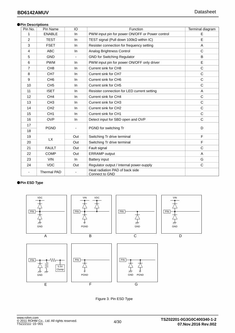
Pin Descriptions
Pin ESD Type
Pin No. Pin Name IO Function Terminal diagram 1 ENABLE In PWM input pin for power ON/OFF or Power control E
2 TEST In TEST signal (Pull down 100kΩ within IC) E
3 FSET In Resister connection for frequency setting A
4 ABC In Analog Brightness Control C
5 GND - GND for Switching Regulator B
6 PWM In PWM input pin for power ON/OFF only driver E
7 CH8 In Current sink for CH8 C
8 CH7 In Current sink for CH7 C
9 CH6 In Current sink for CH6 C
10 CH5 In Current sink for CH5 C
11 ISET In Resister connection for LED current setting A
12 CH4 In Current sink for CH4 C
13 CH3 In Current sink for CH3 C
14 CH2 In Current sink for CH2 C
15 CH1 In Current sink for CH1 C
16 OVP In Detect input for SBD open and OVP C
17 PGND - PGND for switching Tr D
18
19 LX
Out Switching Tr drive terminal F
20 Out Switching Tr drive terminal F
21 FAULT Out Fault signal C
22 COMP Out ERRAMP output A
23 VIN In Battery input G
24 VDC Out Regulator output / Internal power-supply C
- Thermal PAD - Heat radiation PAD of back side Connect to GND
Figure 3. Pin ESD Type

5/30
BD6142AMUV Datasheet
TSZ02201-0G3G0C400340-1-207.Nov.2016 Rev.002
www.rohm.com © 2011 ROHM Co., Ltd. All rights reserved. TSZ22111・15・001
Block Diagram
Pin number 24pin Figure 4. Block diagram
ENABLE
LX
LX
PGND
PGND
VIN VDC
REG TSD
Internal Power Supply Clamp
Internal Power Control
UVLO Internal Reset
FAULT DETECTOR
FAULT
Output short PROTECT
Output Over Voltage PROTECT
LED TERMINAL OPEN/SHORT DETECTOR
LED
RETURN
SELECT
CH1
CH 2
CH 3
CH 4
CH 5
CH 6
CH 7
CH 8
OVP
+
-
Current SENSE
Over Current Protect
Soft start
Control
SENSE
OSC +
ERRAMP
PWM COMP
8ch
GND
Current Driver
+
-
PWM ISET
ISET Resistor driver
COMP TEST FSET ABC
Clamp
6/30
BD6142AMUV Datasheet
TSZ02201-0G3G0C400340-1-207.Nov.2016 Rev.002
www.rohm.com © 2011 ROHM Co., Ltd. All rights reserved. TSZ22111・15・001
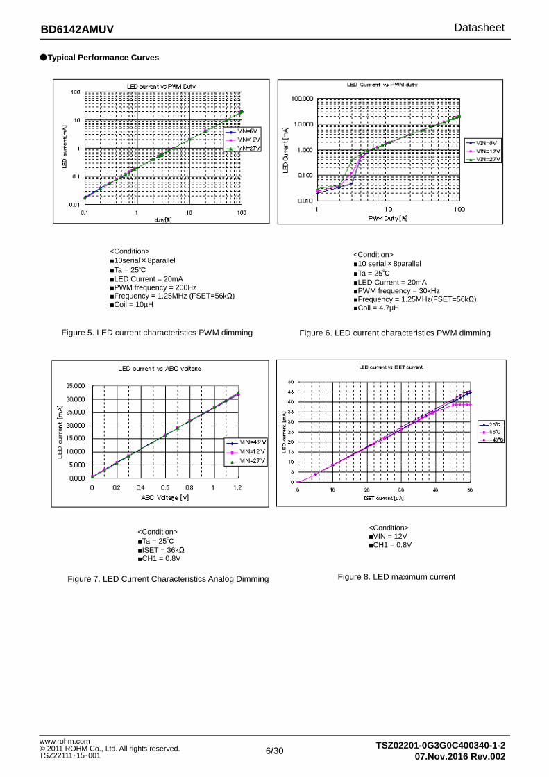
Typical Performance Curves
<Condition> Ta = 25 ISET = 36kΩ CH1 = 0.8V
<Condition> 10serial×8parallel Ta = 25 LED Current = 20mA PWM frequency = 200Hz Frequency = 1.25MHz (FSET=56kΩ) Coil = 10µH
Figure 5. LED current characteristics PWM dimming
<Condition> 10 serial×8parallel Ta = 25 LED Current = 20mA PWM frequency = 30kHz Frequency = 1.25MHz(FSET=56kΩ) Coil = 4.7µH
Figure 6. LED current characteristics PWM dimming
LE
D C
urre
nt [m
A]
LED
Cur
rent
[mA
]
Figure 7. LED Current Characteristics Analog Dimming
Figure 8. LED maximum current
<Condition> VIN = 12V CH1 = 0.8V

7/30
BD6142AMUV Datasheet
TSZ02201-0G3G0C400340-1-207.Nov.2016 Rev.002
www.rohm.com © 2011 ROHM Co., Ltd. All rights reserved. TSZ22111・15・001
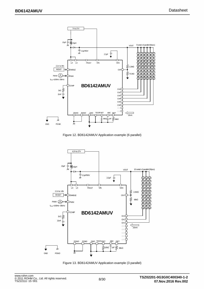
Application example
Figure 11, Figure 12 and Figure 13 are Application examples (15.4inch and 12inch and 10.1inch model). Recommended schematics and Layout are shown in P22.
Figure 11. BD6142AMUV Application example (8 parallel)
<Condition> Ta = 25 10 serial×8parallel LED Current = 20mA Coil = TDK, LTF5022T-100M1R4-LC
Figure 9. Efficiency
<Condition> Ta = 25 10 serial×6parallel LED Current = 20mA Coil = TDK, LTF5022T-100M1R4-LC
Figure 10. Efficiency
BD6142AMUV CH1
CH2
CH3
CH4
CH5
CH6
CH7
CH8
OVP
10 serial x 8 parallel (80pcs)
20mA ABC
LX LX
2.2µF/50V
FAULT VIN
10µH 10µF
ENABLE
PWM
2.1V to VIN
COMP
1kΩ
ISET
36kΩ
GND PGND
PWM
fPWM=100Hz~25kHz
VDC
PGND
22nF
2.2MΩ
68kΩ
VOUT
2.2µF
GND PGND
FSET TEST
56kΩ 1nF
7V to 27V
RESET
8/30
BD6142AMUV Datasheet
TSZ02201-0G3G0C400340-1-207.Nov.2016 Rev.002
www.rohm.com © 2011 ROHM Co., Ltd. All rights reserved. TSZ22111・15・001
Figure 12. BD6142AMUV Application example (6 parallel)
Figure 13. BD6142AMUV Application example (3 parallel)
BD6142AMUV CH1
CH2
CH3
CH4
CH5
CH6
CH7
CH8
OVP
10 serial x 3 parallel (30pcs)
20mA
ABC
LX LX
2.2µF/50V
FAULT VIN
10µH 10µF
4.2V to 27V
ENABLE RESET
PWM
2.1V to VIN
COMP
1kΩ
ISET
36kΩ
GND PGND
PWM
fPWM=100Hz~25kHz
VDC
PGND
22nF
2.2MΩ
68kΩ
VOUT
2.2µF
GND PGND
FSET TEST
110kΩ 1nF
BD6142AMUV CH1
CH2
CH3
CH4
CH5
CH6
CH7
CH8
OVP
9 serial x 6 parallel (54pcs)
20mA ABC
LX LX
2.2µF/50V
FAULT VIN
10µH 10µF
7V to 27V
ENABLE RESET
PWM
2.1V to VIN
COMP
1kΩ
ISET
36kΩ
GND PGND
PWM
fPWM=100Hz~25kHz
VDC
PGND
22nF
2.2MΩ
73.2kΩ
VOUT
2.2µF
GND PGND
FSET TEST
56kΩ 1nF
9/30
BD6142AMUV Datasheet
TSZ02201-0G3G0C400340-1-207.Nov.2016 Rev.002
www.rohm.com © 2011 ROHM Co., Ltd. All rights reserved. TSZ22111・15・001
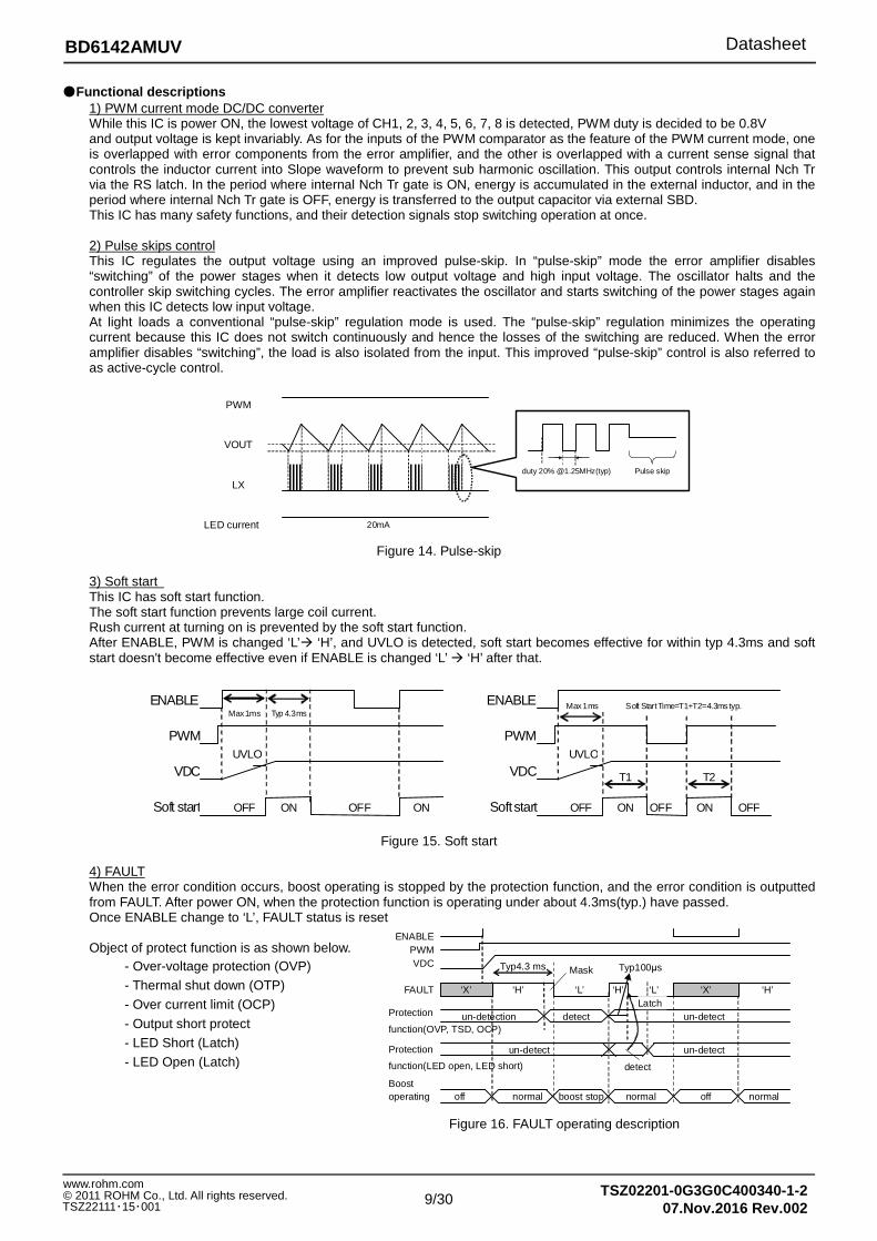
Functional descriptions 1) PWM current mode DC/DC converter While this IC is power ON, the lowest voltage of CH1, 2, 3, 4, 5, 6, 7, 8 is detected, PWM duty is decided to be 0.8V and output voltage is kept invariably. As for the inputs of the PWM comparator as the feature of the PWM current mode, one is overlapped with error components from the error amplifier, and the other is overlapped with a current sense signal that controls the inductor current into Slope waveform to prevent sub harmonic oscillation. This output controls internal Nch Tr via the RS latch. In the period where internal Nch Tr gate is ON, energy is accumulated in the external inductor, and in the period where internal Nch Tr gate is OFF, energy is transferred to the output capacitor via external SBD. This IC has many safety functions, and their detection signals stop switching operation at once. 2) Pulse skips control This IC regulates the output voltage using an improved pulse-skip. In “pulse-skip” mode the error amplifier disables “switching” of the power stages when it detects low output voltage and high input voltage. The oscillator halts and the controller skip switching cycles. The error amplifier reactivates the oscillator and starts switching of the power stages again when this IC detects low input voltage. At light loads a conventional “pulse-skip” regulation mode is used. The “pulse-skip” regulation minimizes the operating current because this IC does not switch continuously and hence the losses of the switching are reduced. When the error amplifier disables “switching”, the load is also isolated from the input. This improved “pulse-skip” control is also referred to as active-cycle control.
Figure 14. Pulse-skip
3) Soft start This IC has soft start function. The soft start function prevents large coil current. Rush current at turning on is prevented by the soft start function. After ENABLE, PWM is changed ‘L’ ‘H’, and UVLO is detected, soft start becomes effective for within typ 4.3ms and soft start doesn't become effective even if ENABLE is changed ‘L’ ‘H’ after that.
Figure 15. Soft start
4) FAULT When the error condition occurs, boost operating is stopped by the protection function, and the error condition is outputted from FAULT. After power ON, when the protection function is operating under about 4.3ms(typ.) have passed. Once ENABLE change to ‘L’, FAULT status is reset Object of protect function is as shown below.
- Over-voltage protection (OVP) - Thermal shut down (OTP) - Over current limit (OCP)
- Output short protect - LED Short (Latch) - LED Open (Latch)
Figure 16. FAULT operating description
off normal boost stop normal off normal
un-detection detect un-detect
Typ4.3 ms
FAULT
Protection
function(OVP, TSD, OCP)
Boost operating
VDCPWM
‘X’ ‘X’ ‘H’ ‘L’ ‘H’ ‘L’ ‘H’
Mask
un-detectProtection
function(LED open, LED short) detect
un-detect
Latch
Typ100µs
ENABLE
PWM
VOUT
LED current
LX
20mA
duty 20% @1.25MHz(typ) Pulse skip
PWMUVLO
ENABLE Max 1ms Typ 4.3ms
OFF ON OFF ON
VDC
Soft start
ENABLE Max 1ms
OFF ON OFF ON
VDC
Soft start
PWM UVLO
OFF
T1 T2
Soft Start Time=T1+T2=4.3ms typ.

10/30
BD6142AMUV Datasheet
TSZ02201-0G3G0C400340-1-207.Nov.2016 Rev.002
www.rohm.com © 2011 ROHM Co., Ltd. All rights reserved. TSZ22111・15・001
Protection PROTECTION TABLE
CASE FAILURE MODE
DETECTION MODE
FAIL CHANNEL
GOOD CHANNEL
VOUT REGULATED BY
FAULT Terminal
1 LED Short connected CH1
CH1 > VSC(5V) LED current stop and DC/DC feedback doesn’t return
CH2 to CH8 Normal
Highest VF of CH2 to CH8
‘H’ ‘L’ (Latch)
2 LED OPEN connected CH1
CH1 < 0.2V and VOUT > VOVP
LED current stop and DC/DC feedback doesn’t return
CH2 to CH8 Normal
Highest VF of CH2 to CH8
‘H’ ‘L’ (Latch)
3 VOUT/LX GND SHORT
OVP < 50mV FAULT change from L to H, and switching is stopped. When OVP>50mV, FAULT return L
- ‘H’ ‘L’
4 Output LED stack voltage too high
VOUT > VOVP FAULT change from L to H, and switching is stopped. Even if OVP<1.2V, FAULT don’t return L
- ‘H’ ‘L’
5
LX current too high
OCP > 2.5A or OTP > 130°C
FAULT change from L to H, and switching is stopped. Even if IC return normal status, FAULT don’t return L
-
‘H’ ‘L’
・Over voltage protection (OVP) At such an error of output open as the output DC/DC and the LED is not connected to IC, the DC/DC will boost too much and the OVP terminal exceed the absolute maximum ratings, and may destruct the IC. Therefore, when OVP terminal becomes sensing voltage or higher, the over voltage limit protection works, and turns off the switching Tr, and DC/DC will be stopped. At this moment, the IC changes from activation into non-activation, and the output voltage goes down slowly. And, when the Feedback of CH1 isn’t returned, so that VOUT will return normal voltage.
Figure 17. OVP operating description
VOUT
CH1 voltage
CH1 connection
CH2 connection
Feedback
ENABLE, PWM
connect
CH1 CH1 CH2
connect
open
CH1 current 20mA 0mA
CH2 current 20mA 0mA
OVP Signal
Hysteresis(typ 2.5%)

11/30
BD6142AMUV Datasheet
TSZ02201-0G3G0C400340-1-207.Nov.2016 Rev.002
www.rohm.com © 2011 ROHM Co., Ltd. All rights reserved. TSZ22111・15・001
This section is especially mentioned here because the spec shown electrical characteristic is necessary to explain this section.
Over voltage limit min 1.16V typ 1.20V max 1.24V LED control voltage min 0.64V typ 0.80V max 0.96V LED terminal over voltage protect min 4.25V typ 5.00 V max 5.75V
1. Calculate the conditions that the total value of LED VF is MAX. Example) In the case of serial 8 LEDs with VF=2.9V(min), 3.2V(typ), 3.5V(max) => 3.5V x 8=28V
2. Then calculate the biggest value of output with the following formula. The biggest value of output = the biggest value calculated for 1 + the biggest value of LED terminal voltage. (0.96V) Example) The biggest value of output = 28V + 0.96V =28.96V
3. Set the smallest value of over voltage larger than the biggest value of output. If over voltage is closer to the total value of VF, it could be occurred to detect over voltage by ripple, noise, and so on. It is recommended that some margins should be left on the difference between over voltage and the total value of VF. This time around 6% margin is placed. Example) Against the biggest value of output = 28.96V, the smallest value of over voltage = 28.96V x 1.06 = 30.70V Ic over voltage limit min=1.16V, typ=1.20V, max=1.24V
typ = 30.70V×(1.20V/1.16V) = 31.76V max = 31.76V×(1.26V/1.20V) = 33.35V
4. The below shows how to control resistor setting over voltage
Please fix resistor high between OVP terminal and output and then set over voltage after changing resistor between OVP terminal and GND. While PWM is off, output voltage decreases by minimizing this resistor. Due to the decrease of output voltage, ripple of output voltage increases, and singing of output condenser also becomes bigger. Example) Selecting OVP resistor.
・・・・OVP resistor selection (Example. 1) VF=3.5V max, serial = 7 LED
OVP = 1.2V, R1 = 2.2MΩ, R2 = 95.3kΩ VOUT = 1.2 × (2.2MΩ + 95.3kΩ)/ 95.3kΩ = 28.90V
(Example. 2) VF=3.5V max, serial = 8 LED OVP = 1.2V, R1 = 2.2MΩ, R2 = 82kΩ VOUT = 1.2 × (2.2MΩ + 82kΩ)/ 82kΩ = 33.40V
(Example. 3) VF=3.5V max, serial = 9 LED OVP = 1.2V, R1 = 2.2MΩ, R2 = 73.2kΩ VOUT = 1.2 × (2.2MΩ + 73.2kΩ)/ 73.2kΩ = 37.27V
(Example. 4) VF=3.5V max, serial = 10 LED OVP = 1.2V, R1 = 2.2MΩ, R2 = 68kΩ VOUT = 1.2 × (2.2MΩ + 68kΩ)/ 68kΩ = 40.02V
・External SBD open detect / Output Short protection In the case of external SBD is not connected to IC, or VOUT is shorted to GND, the coil or internal Tr may be destructed. Therefore, at such an error as OVP becoming 50mV(typ.) or below, turns off the output Tr, and prevents the coil and the IC from being destructed. And the IC changes from activation into non-activation, and current does not flow to the coil (0mA). ・Thermal shut down This IC has thermal shut down function. The thermal shut down works at 130°C (typ.) or higher, and the IC changes from activation into non-activation.
OVP terminal
VOUT
R1
R2
12/30
BD6142AMUV Datasheet
TSZ02201-0G3G0C400340-1-207.Nov.2016 Rev.002
www.rohm.com © 2011 ROHM Co., Ltd. All rights reserved. TSZ22111・15・001
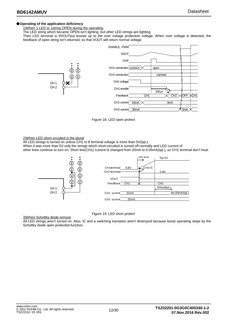
Operating of the application deficiency 1)When 1 LED or 1string OPEN during the operating The LED string which became OPEN isn't lighting, but other LED strings are lighting. Then LED terminal is 0VOUTput boosts up to the over voltage protection voltage. When over voltage is detected, the feedback of open string isn’t returned, so that VOUT will return normal voltage.
2)When LED short-circuited in the plural All LED strings is turned on unless CH1 to 8 terminal voltage is more than 5V(typ.). When it was more than 5V only the strings which short-circuited is turned off normally and LED current of other lines continue to turn on. Short line(CH1) current is changed from 20mA to 0.05mA(typ.), so CH1 terminal don’t heat.
3)When Schottky diode remove All LED strings aren’t turned on. Also, IC and a switching transistor aren't destroyed because boost operating stops by the Schottky diode open protected function.
CH 1 CH 2
CH 1 CH 2
Figure 18. LED open protect
Figure 19. LED short protect
VOUT
CH1 voltage
CH1 connection
CH2 connection
Feedback
ENABLE, PWM
CH1 current
connect
CH1 OFF CH2
connect
open
20mA 0mA
CH2 current 20mA 0mA
CH1
OVP
CH1 enable100µs
CH1terminal
FeedBack
CH1 current
CH1 CH2
CH2 current 20mA
20mA 0.05mA(typ.)
VOUT
0.8V
LED short
CH2 terminal 0.8V
Typ 5V
CH1>CH2
100µs(typ.)
13/30
BD6142AMUV Datasheet
TSZ02201-0G3G0C400340-1-207.Nov.2016 Rev.002
www.rohm.com © 2011 ROHM Co., Ltd. All rights reserved. TSZ22111・15・001
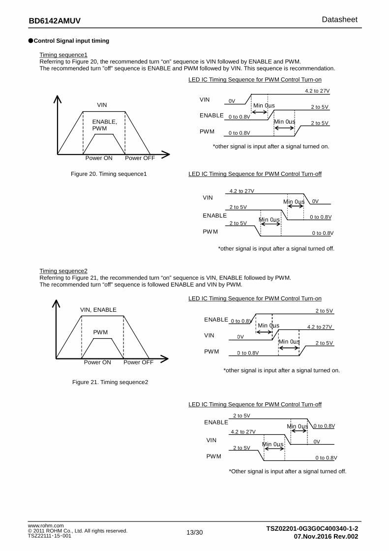
Control Signal input timing
Timing sequence1 Referring to Figure 20, the recommended turn “on” sequence is VIN followed by ENABLE and PWM. The recommended turn ”off” sequence is ENABLE and PWM followed by VIN. This sequence is recommendation.
Timing sequence2 Referring to Figure 21, the recommended turn “on” sequence is VIN, ENABLE followed by PWM. The recommended turn “off” sequence is followed ENABLE and VIN by PWM.
ENABLE, PWM
VIN
Power ON Power OFF
LED IC Timing Sequence for PWM Control Turn-on
VIN 2 to 5V Min 0µs
PWM
ENABLE Min 0µs
4.2 to 27V
2 to 5V
0 to 0.8V
0 to 0.8V
0V
LED IC Timing Sequence for PWM Control Turn-off
PW M
2 to 5V Min 0µs
VIN
ENABLE Min 0µs
4.2 to 27V
2 to 5V
0 to 0.8V
0 to 0.8V
0V
Figure 20. Timing sequence1
PWM
VIN, ENABLE
Power ON Power OFF
ENABLE
2 to 5V
Min 0µs
VIN
PWM
Min 0µs
4.2 to 27V
2 to 5V
0 to 0.8V
0 to 0.8V
0V
VIN
2 to 5V
Min 0µs ENABLE
PWM
Min 0µs
4.2 to 27V
2 to 5V
0 to 0.8V
0 to 0.8V
0V
LED IC Timing Sequence for PWM Control Turn-on
Figure 21. Timing sequence2
LED IC Timing Sequence for PWM Control Turn-off
*other signal is input after a signal turned on.
*other signal is input after a signal turned off.
*Other signal is input after a signal turned off.
*other signal is input after a signal turned on.
14/30
BD6142AMUV Datasheet
TSZ02201-0G3G0C400340-1-207.Nov.2016 Rev.002
www.rohm.com © 2011 ROHM Co., Ltd. All rights reserved. TSZ22111・15・001
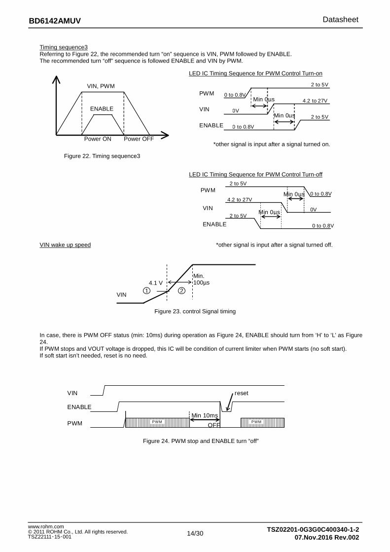
Timing sequence3 Referring to Figure 22, the recommended turn “on” sequence is VIN, PWM followed by ENABLE. The recommended turn “off” sequence is followed ENABLE and VIN by PWM.
VIN wake up speed
Figure 23. control Signal timing
In case, there is PWM OFF status (min: 10ms) during operation as Figure 24, ENABLE should turn from ‘H’ to ‘L’ as Figure 24. If PWM stops and VOUT voltage is dropped, this IC will be condition of current limiter when PWM starts (no soft start). If soft start isn’t needed, reset is no need.
VIN
Min. 100µs 4.1 V
1 2
Figure 24. PWM stop and ENABLE turn “off”
PWM OFF
VIN
ENABLE Min 10ms
reset
PWM PWM
ENABLE
VIN, PWM
Power ON Power OFF
PWM
2 to 5V
Min 0µs
VIN
ENABLE
Min 0µs
4.2 to 27V
2 to 5V
0 to 0.8V
0 to 0.8V
0V
VIN
2 to 5V
Min 0µs PWM
ENABLE
Min 0µs
4.2 to 27V
2 to 5V
0 to 0.8V
0 to 0.8V
0V
LED IC Timing Sequence for PWM Control Turn-on
Figure 22. Timing sequence3
LED IC Timing Sequence for PWM Control Turn-off
*other signal is input after a signal turned on.
*other signal is input after a signal turned off.

15/30
BD6142AMUV Datasheet
TSZ02201-0G3G0C400340-1-207.Nov.2016 Rev.002
www.rohm.com © 2011 ROHM Co., Ltd. All rights reserved. TSZ22111・15・001
How to activate Please be careful about the following when being activated.
- Regulator (VDC) operates after ENABLE=H. Inside circuit operates after releasing UVLO. When IC boosts after releasing UVLO, soft start function operates. (Refer to Figure 15, 9P). Soft start circuit needs t15 (more than 15µs) as Figure 25. shows. Soft start operates for tsoft time. Please make H width of PWM more than 15µs until soft start finishes.
- Please input PWM signal according to Figure 26. after soft start finishes.
Figure 25. Soft start
Example) Time until soft start finishes at PWM frequency 25kHz and PWM=H time16µs According to soft start time typ4.3ms tsoft = 16µs – 15µs = 1µs Soft start time/ tsoft /PWM frequency = 4300µs / 1µs /25kHz = 4300 / 25kHz = 172ms
Figure 26. Input timing (after soft start)
Name Unit Min. Typ. Max.
t1 Power supply rising time µs 100 - - t2 Power supply-ENABLE time µs 0 - - t3 ENABLE rising time µs 0 - 100 t4 ENABLE falling time µs 0 - 100 t5 ENABLE low width µs 50 - - t6 Power supply-PWM time µs 0 - - t7 PWM rising time µs 0 - 100 t8 PWM high width µs 5 - - t9 PWM falling time µs 0 - 100
t10 PWM low width µs 5 - - t11 PWM frequency µs 40 5000 10000 t12 ENABLE (H)->PWM (H) time µs 0 - - t13 ENABLE (L)->PWM (L) time µs 0 - - t14 PWM (L)->ENABLE (L) time µs 0 - - t15 PWM high width (while soft start) µs 15 - - H Operating voltage V 4.2 12 27 L Non operating voltage V - - 4.2
L[V]VIN
VDC
ENABLE
t1
H[V]
t2 t3
t14
t6
t10
t11
t7 t9 t8
t4 t5
H[V]
PWM
t14
t3
At light dimming of PWM terminal (after soft start finishes)
VIN
VDC
ENABLE
UVLO
PWM
SOFT START
Over current value increases..
t15
tsoft
tsoft
tsoft

16/30
BD6142AMUV Datasheet
TSZ02201-0G3G0C400340-1-207.Nov.2016 Rev.002
www.rohm.com © 2011 ROHM Co., Ltd. All rights reserved. TSZ22111・15・001
How to select the number of LED strings of the curre nt driver When the number of LED strings of the current driver is reduced, the un-select can be set the matter that the unnecessary CH1 to 8 terminal is opened. When it uses with 6 lines and so on, it can correspond to it by becoming 2 unnecessary lines to open. When VOUT wake up, VOUT boost up until OVP voltage. Once IC detect OVP, VOUT don’t boost up until OVP from next start up. To set PWM and ENABLE to L, IC reset CH7, 8 status as Figure 27. When VOUT wake up, CH8 (open terminal) and CH1 are selected as Figure 28.
Figure 27. Select the number of CH lines 1
Figure 28. Select the number of CH lines 2 (wake up)
CH 1 CH 2 CH 3 CH 4 CH 5
CH 7 CH 6
CH 8
PWM
ENABLE
VOUT
CH1 to 6
CH7 to 8
OVP
Normal voltage
0.8V(typ.) 0V
0V
Reset
Mask
open
CH1 Current
CH8 Terminal
CH8 Current
20mA
Vout
Soft start: typ 4.3ms
ENABLE
Stable
PWM
CH1 Terminal
0mA
0mA
Feedback terminal
Typ 0.8V
Over voltage protect signal
“Unmask Terminal select(LED open protect)
se
CH1 CH8
Normal condition
Over Voltage Protect
100µs(typ.)

17/30
BD6142AMUV Datasheet
TSZ02201-0G3G0C400340-1-207.Nov.2016 Rev.002
www.rohm.com © 2011 ROHM Co., Ltd. All rights reserved. TSZ22111・15・001
Start control (ENABLE) and select LED current driver (PWM) This IC can control the IC system by ENABLE, and IC can power off compulsory by setting 0.8V or below. Also, It powers on ENABLE is at more than 2.0V. After it’s selected to ENABLE=H, When it is selected at PWM=H, LED current decided with ISET resistance flow. Next, When it is selected at PWM=L, LED current stop to flow.
ENABLE PWM IC LED current
0 0 Off OFF
1 0 On OFF
0 1 Off OFF
1 1 On Current decided with ISET
LED current setting range
LED current can set up Normal current by resistance value (RISET) connecting to ISET voltage. Setting of each LED current is given as shown below.
RISET = 720/ILEDmax Also, Normal current setting range is 10mA to 30mA. LED current becomes a leak current MAX 2µA at OFF setting.
ISET Normal current setting example
RISET LED current
24kΩ (E24) 30.0mA
30kΩ (E24) 24.0mA
36kΩ (E24) 20.0mA
43kΩ (E24) 16.7mA
68kΩ (E12) 10.6mA
Frequency setting range
Switching frequency can be set up by resistance value (RFSET) connecting to FSET port. Setting of frequency is given as shown below. Also, Frequency setting range is 0.60MHz to 1.60MHz.
FSET frequency setting example
RFSET frequency
130kΩ (E96) 0.57MHz
56kΩ (E24) 1.25MHz
43kΩ (E24) 1.59MHz
Max Duty example
Frequency Max Duty[%]
Min Typ Max
0.57MHz - 96.0 -
1.25MHz 91.0 95.0 99.0
1.59MHz - 92.0 -
Min Duty example
Frequency Min Duty[%]
Min Typ Max
1.25MHz - 20 -
Frequency [MHz]
1.25
56kΩ 130 kΩ FSET[kΩ]
0.57
1.59
43 kΩ
18/30
BD6142AMUV Datasheet
TSZ02201-0G3G0C400340-1-207.Nov.2016 Rev.002
www.rohm.com © 2011 ROHM Co., Ltd. All rights reserved. TSZ22111・15・001
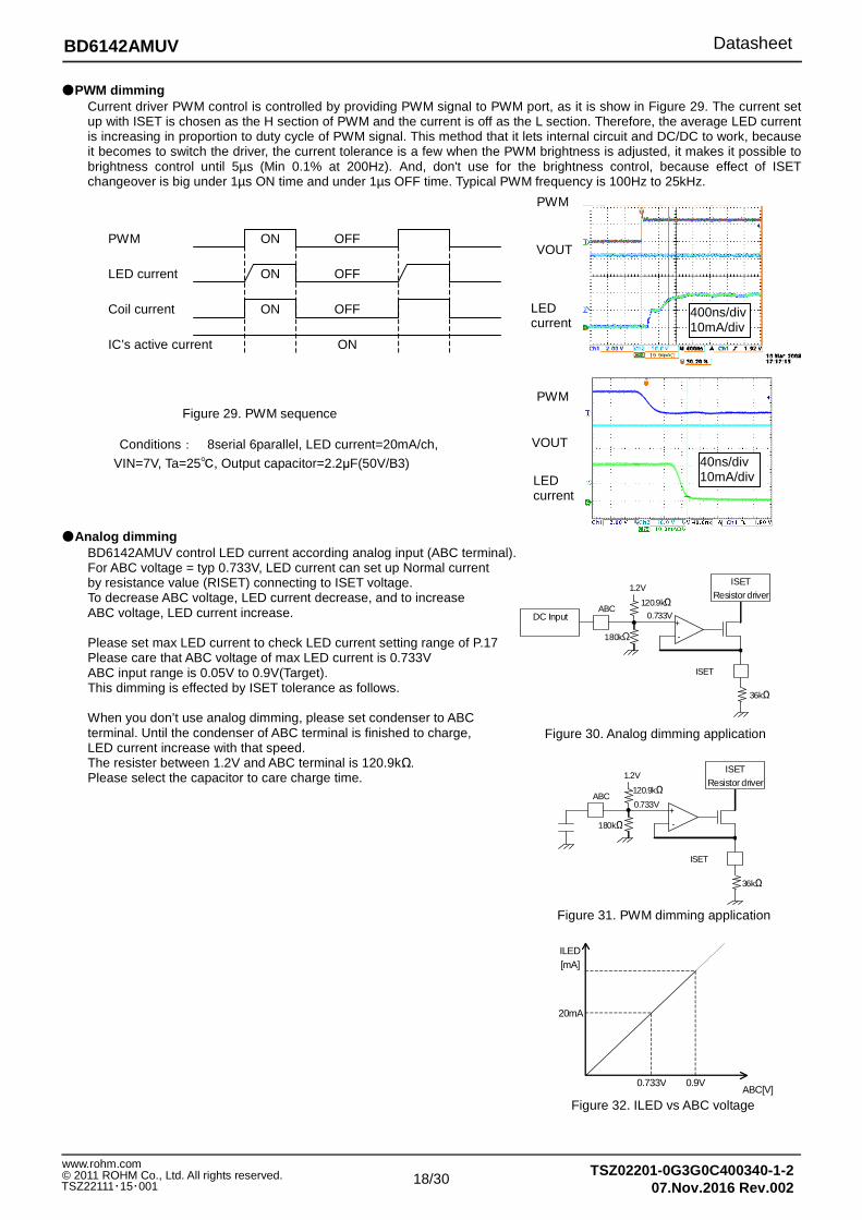
PWM dimming Current driver PWM control is controlled by providing PWM signal to PWM port, as it is show in Figure 29. The current set up with ISET is chosen as the H section of PWM and the current is off as the L section. Therefore, the average LED current is increasing in proportion to duty cycle of PWM signal. This method that it lets internal circuit and DC/DC to work, because it becomes to switch the driver, the current tolerance is a few when the PWM brightness is adjusted, it makes it possible to brightness control until 5µs (Min 0.1% at 200Hz). And, don't use for the brightness control, because effect of ISET changeover is big under 1µs ON time and under 1µs OFF time. Typical PWM frequency is 100Hz to 25kHz.
Conditions: 8serial 6parallel, LED current=20mA/ch,
VIN=7V, Ta=25, Output capacitor=2.2µF(50V/B3)
Analog dimming
BD6142AMUV control LED current according analog input (ABC terminal). For ABC voltage = typ 0.733V, LED current can set up Normal current by resistance value (RISET) connecting to ISET voltage. To decrease ABC voltage, LED current decrease, and to increase ABC voltage, LED current increase. Please set max LED current to check LED current setting range of P.17 Please care that ABC voltage of max LED current is 0.733V ABC input range is 0.05V to 0.9V(Target). This dimming is effected by ISET tolerance as follows. When you don’t use analog dimming, please set condenser to ABC terminal. Until the condenser of ABC terminal is finished to charge, LED current increase with that speed. The resister between 1.2V and ABC terminal is 120.9kΩ. Please select the capacitor to care charge time.
PWM
LED current
Coil current
IC’s active current
ON OFF
ON OFF
ON OFF
ON
Figure 29. PWM sequence
ISET
+
-
ISET Resistor driver
ABC
1.2V
0.733V DC Input
120.9kΩ
36kΩ
180kΩ
ISET
+
-
ISET Resistor driver
ABC
1.2V
0.733V
120.9kΩ
180kΩ
36kΩ
Figure 30. Analog dimming application
Figure 31. PWM dimming application
ILED [mA]
20mA
0.733V 0.9V ABC[V]
Figure 32. ILED vs ABC voltage
PWM
VOUT
LED current
VOUT
PWM
400ns/div 10mA/div
LED current
40ns/div 10mA/div
19/30
BD6142AMUV Datasheet
TSZ02201-0G3G0C400340-1-207.Nov.2016 Rev.002
www.rohm.com © 2011 ROHM Co., Ltd. All rights reserved. TSZ22111・15・001
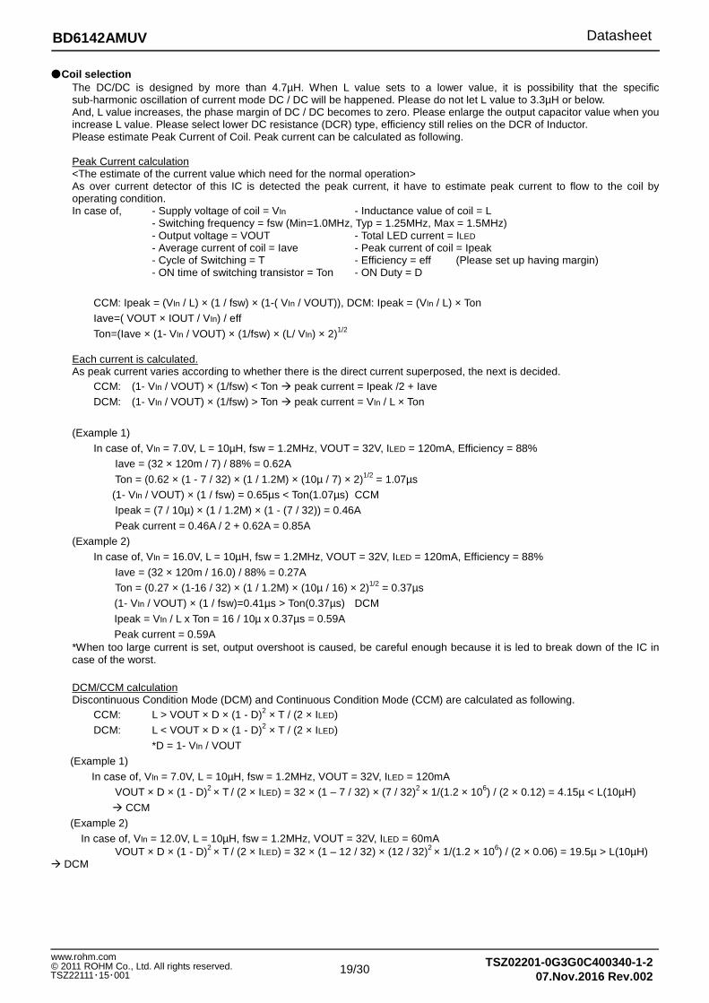
Coil selection The DC/DC is designed by more than 4.7µH. When L value sets to a lower value, it is possibility that the specific sub-harmonic oscillation of current mode DC / DC will be happened. Please do not let L value to 3.3µH or below. And, L value increases, the phase margin of DC / DC becomes to zero. Please enlarge the output capacitor value when you increase L value. Please select lower DC resistance (DCR) type, efficiency still relies on the DCR of Inductor. Please estimate Peak Current of Coil. Peak current can be calculated as following. Peak Current calculation <The estimate of the current value which need for the normal operation> As over current detector of this IC is detected the peak current, it have to estimate peak current to flow to the coil by operating condition. In case of, - Supply voltage of coil = VIn - Inductance value of coil = L - Switching frequency = fsw (Min=1.0MHz, Typ = 1.25MHz, Max = 1.5MHz) - Output voltage = VOUT - Total LED current = ILED - Average current of coil = Iave - Peak current of coil = Ipeak - Cycle of Switching = T - Efficiency = eff (Please set up having margin) - ON time of switching transistor = Ton - ON Duty = D
CCM: Ipeak = (VIn / L) × (1 / fsw) × (1-( VIn / VOUT)), DCM: Ipeak = (VIn / L) × Ton
Iave=( VOUT × IOUT / VIn) / eff
Ton=(Iave × (1- VIn / VOUT) × (1/fsw) × (L/ VIn) × 2)1/2
Each current is calculated. As peak current varies according to whether there is the direct current superposed, the next is decided.
CCM: (1- VIn / VOUT) × (1/fsw) < Ton peak current = Ipeak /2 + Iave
DCM: (1- VIn / VOUT) × (1/fsw) > Ton peak current = VIn / L × Ton
(Example 1)
In case of, VIn = 7.0V, L = 10µH, fsw = 1.2MHz, VOUT = 32V, ILED = 120mA, Efficiency = 88%
Iave = (32 × 120m / 7) / 88% = 0.62A
Ton = (0.62 × (1 - 7 / 32) × (1 / 1.2M) × (10µ / 7) × 2)1/2 = 1.07µs
(1- VIn / VOUT) × (1 / fsw) = 0.65µs < Ton(1.07µs) CCM
Ipeak = (7 / 10µ) × (1 / 1.2M) × (1 - (7 / 32)) = 0.46A
Peak current = 0.46A / 2 + 0.62A = 0.85A
(Example 2)
In case of, VIn = 16.0V, L = 10µH, fsw = 1.2MHz, VOUT = 32V, ILED = 120mA, Efficiency = 88%
Iave = (32 × 120m / 16.0) / 88% = 0.27A
Ton = (0.27 × (1-16 / 32) × (1 / 1.2M) × (10µ / 16) × 2)1/2 = 0.37µs
(1- VIn / VOUT) × (1 / fsw)=0.41µs > Ton(0.37µs) DCM
Ipeak = VIn / L x Ton = 16 / 10µ x 0.37µs = 0.59A
Peak current = 0.59A *When too large current is set, output overshoot is caused, be careful enough because it is led to break down of the IC in case of the worst.
DCM/CCM calculation Discontinuous Condition Mode (DCM) and Continuous Condition Mode (CCM) are calculated as following.
CCM: L > VOUT × D × (1 - D)2 × T / (2 × ILED)
DCM: L < VOUT × D × (1 - D)2 × T / (2 × ILED)
*D = 1- VIn / VOUT
(Example 1)
In case of, VIn = 7.0V, L = 10µH, fsw = 1.2MHz, VOUT = 32V, ILED = 120mA
VOUT × D × (1 - D)2 × T / (2 × ILED) = 32 × (1 – 7 / 32) × (7 / 32)2 × 1/(1.2 × 106) / (2 × 0.12) = 4.15µ < L(10µH)
CCM
(Example 2)
In case of, VIn = 12.0V, L = 10µH, fsw = 1.2MHz, VOUT = 32V, ILED = 60mA VOUT × D × (1 - D)2 × T / (2 × ILED) = 32 × (1 – 12 / 32) × (12 / 32)2 × 1/(1.2 × 106) / (2 × 0.06) = 19.5µ > L(10µH)
DCM

20/30
BD6142AMUV Datasheet
TSZ02201-0G3G0C400340-1-207.Nov.2016 Rev.002
www.rohm.com © 2011 ROHM Co., Ltd. All rights reserved. TSZ22111・15・001
OUTPUT Capacitor selection Output Capacitor smoothly keeps output voltage and supplies LED current. Output Voltage consists of Charge (FET ON) and Discharge (LED current). So Output voltage has Output ripple Voltage every FET switching. Output ripple voltage is calculated as following. Output ripple Voltage
- Switching cycle = T - Total LED current = ILED
- Switching ON duty = D - Output ripple Voltage = Vripple
- Output Capacitor = COUT - Output Capacitor (real value) = Creal
- Decreasing ratio of Capacitor = Cerror
Creal = COUT × Cerror (Capacitor value is decreased by Bias, so)
Creal = ILED × D × T / Vripple
COUT = ILED × D × T / Vripple / Cerror
(Example 1)
In case of, VIN=12.0V, fsw = 1.2MHz, VOUT =32V, ILED =120mA, COUT = 8.8µF, Cerror = 50%
T = 1 / 1.2MHz
D = 1 – VIN / VOUT = 1 – 12/32
Vripple = ILED × (1 – D) × T / (COUT×Cerror) = 120mA × (12/32) / 1.2MHz / (8.8µF×0.5)
= 8.5mV
0V 35V 50V Output voltage
Ca
pa [
µF]
COUT
Creal
Figure 33. Bias Characteristics of Capacitor
21/30
BD6142AMUV Datasheet
TSZ02201-0G3G0C400340-1-207.Nov.2016 Rev.002
www.rohm.com © 2011 ROHM Co., Ltd. All rights reserved. TSZ22111・15・001
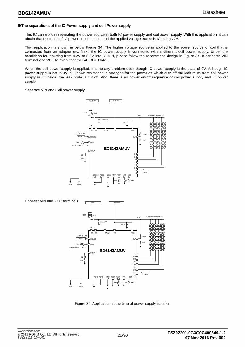
The separations of the IC Power supply and coil Power supply This IC can work in separating the power source in both IC power supply and coil power supply. With this application, it can obtain that decrease of IC power consumption, and the applied voltage exceeds IC rating 27V. That application is shown in below Figure 34. The higher voltage source is applied to the power source of coil that is connected from an adapter etc. Next, the IC power supply is connected with a different coil power supply. Under the conditions for inputting from 4.2V to 5.5V into IC VIN, please follow the recommend design in Figure 34. It connects VIN terminal and VDC terminal together at ICOUTside. When the coil power supply is applied, it is no any problem even though IC power supply is the state of 0V. Although IC power supply is set to 0V, pull-down resistance is arranged for the power off which cuts off the leak route from coil power supply in IC inside, the leak route is cut off. And, there is no power on-off sequence of coil power supply and IC power supply. Separate VIN and Coil power supply Connect VIN and VDC terminals
Figure 34. Application at the time of power supply isolation
BD6142AMUV CH1
CH2
CH3
CH4
CH5
CH6
CH7
CH8
OVP
10 serial x 6 parallel (60pcs)
20mA ABC
LX LX
2.2µF/50V
FAULT VIN
10µH 10µF
7V to 27V
ENABLE RESET
PWM
2.1V to VIN
COMP
1kΩ
ISET
36kΩ
GND PGND
PWM
fPWM=100Hz~25kHz
VDC
PGND
22nF
2.2MΩ
68kΩ
VOUT
2.2µF
GND PGND
FSET
4.2V to 30V
TEST
1nF 56 kΩ
BD6142AMUV CH1
CH2
CH3
CH4
CH5
CH6
CH7
CH8
OVP
10 serial x 6 parallel (60pcs)
20mA ABC
LX LX
2.2µF/50V
FAULT VIN
10µH 10µF
4.2V to 5.5V
ENABLE RESET
PWM
2.1V to VIN
COMP
1kΩ
ISET
36kΩ
GND PGND
PWM
fPWM=100Hz~25kHz
VDC
PGND
22nF
2.2MΩ
68kΩ
VOUT
2.2µF
GND PGND
FSET
4.2V to 30V
TEST
56kΩ 1nF
22/30
BD6142AMUV Datasheet
TSZ02201-0G3G0C400340-1-207.Nov.2016 Rev.002
www.rohm.com © 2011 ROHM Co., Ltd. All rights reserved. TSZ22111・15・001
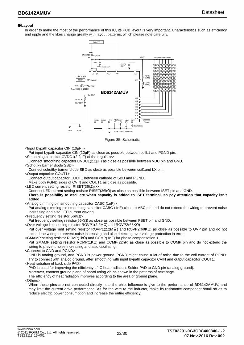
Layout In order to make the most of the performance of this IC, its PCB layout is very important. Characteristics such as efficiency and ripple and the likes change greatly with layout patterns, which please note carefully.
Figure 35. Schematic
<Input bypath capacitor CIN (10µF)> Put input bypath capacitor CIN (10µF) as close as possible between coilL1 and PGND pin.
<Smoothing capacitor CVDC1(2.2µF) of the regulator> Connect smoothing capacitor CVDC1(2.2µF) as close as possible between VDC pin and GND.
<Schottky barrier diode SBD> Connect schottky barrier diode SBD as close as possible between coil1and LX pin.
<Output capacitor COUT1> Connect output capacitor COUT1 between cathode of SBD and PGND. Make both PGND sides of CVIN and COUT1 as close as possible.
<LED current setting resistor RISET(36kΩ)>> Connect LED current setting resistor RISET(36kΩ) as close as possible between ISET pin and GND. There is possibility to oscillate when capacity is added to ISET terminal, so pay attention that capacit y isn’t added.
<Analog dimming pin smoothing capacitor CABC (1nF)> Put analog dimming pin smoothing capacitor CABC (1nF) close to ABC pin and do not extend the wiring to prevent noise increasing and also LED current waving.
<Frequency setting resistor(56KΩ)> Put frequency setting resistor(56KΩ) as close as possible between FSET pin and GND.
<Over voltage limit setting resistor ROVP1(2.2MΩ) and ROVP2(68KΩ) Put over voltage limit setting resistor ROVP1(2.2MΩ) and ROVP2(68KΩ) as close as possible to OVP pin and do not extend the wiring to prevent noise increasing and also detecting over voltage protection in error.
<GMAMP setting resistor RCMP(1kΩ) and CCMP(1nF) for phase compensation > Put GMAMP setting resistor RCMP(1KΩ) and CCMP(22nF) as close as possible to COMP pin and do not extend the wiring to prevent noise increasing and also oscillating.
<Connect to GND and PGND> GND is analog ground, and PGND is power ground. PGND might cause a lot of noise due to the coil current of PGND. Try to connect with analog ground, after smoothing with input bypath capacitor CVIN and output capacitor COUT1.
<Heat radiation of back side PAD> PAD is used for improving the efficiency of IC heat radiation. Solder PAD to GND pin (analog ground). Moreover, connect ground plane of board using via as shown in the patterns of next page. The efficiency of heat radiation improves according to the area of ground plane.
<Others> When those pins are not connected directly near the chip, influence is give to the performance of BD6142AMUV, and may limit the current drive performance. As for the wire to the inductor, make its resistance component small so as to reduce electric power consumption and increase the entire efficiency.
BD6142AMUV CH1
CH2
CH3
CH4
CH5
CH6
CH7
CH8
OVP
10 serial x 8 parallel (80pcs)
20mA ABC
LX LX
COUT1(2.2µF/50V)
FAULT VIN
L1(10µH) CIN(10µF)
7V to 27V
ENABLE RESET
PWM
2.1V to VIN
COMP
RCMP(1kΩ)
ISET
RISET(36kΩ)
GND PGND
PWM
fPWM=100Hz~25kHz
VDC
PGND
CCMP(22nF)
ROVP1 (2.2MΩ)
ROVP2 (68kΩ)
VOUT
CVDC1 (2.2µF)
GND PGND
FSET TEST
SBD
RFSET(56kΩ) CABC(1nF)

23/30
BD6142AMUV Datasheet
TSZ02201-0G3G0C400340-1-207.Nov.2016 Rev.002
www.rohm.com © 2011 ROHM Co., Ltd. All rights reserved. TSZ22111・15・001
Recommended PCB layout
Figure 36. Top Copper trace layer
Figure 37. Middle1 Copper trace layer
Figure 38. Middle2 Copper trace layer
Figure 39. Bottom Copper trace layer
COUT1
SBD
PGND
GND
RISET
ROVP2 ROVP1
RCMP CCMP
L1
CIN
CVDC1
D6 14 2
GND
PGND
Input Voltage
VOUT
RFSET CABC
24/30
BD6142AMUV Datasheet
TSZ02201-0G3G0C400340-1-207.Nov.2016 Rev.002
www.rohm.com © 2011 ROHM Co., Ltd. All rights reserved. TSZ22111・15・001
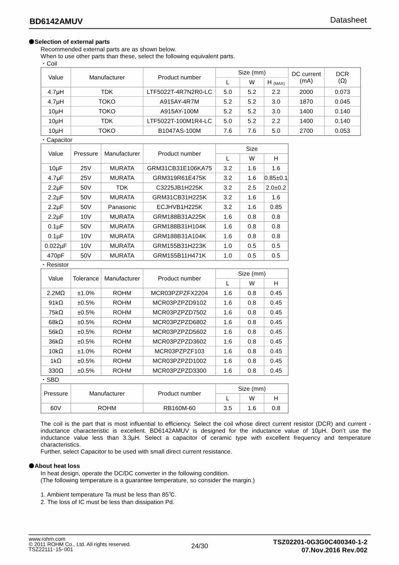
Selection of external parts Recommended external parts are as shown below. When to use other parts than these, select the following equivalent parts. ・Coil
Value Manufacturer Product number Size (mm) DC current
(mA) DCR (Ω) L W H (MAX)
4.7µH TDK LTF5022T-4R7N2R0-LC 5.0 5.2 2.2 2000 0.073
4.7µH TOKO A915AY-4R7M 5.2 5.2 3.0 1870 0.045
10µH TOKO A915AY-100M 5.2 5.2 3.0 1400 0.140
10µH TDK LTF5022T-100M1R4-LC 5.0 5.2 2.2 1400 0.140
10µH TOKO B1047AS-100M 7.6 7.6 5.0 2700 0.053
・Capacitor
Value Pressure Manufacturer Product number Size
L W H
10µF 25V MURATA GRM31CB31E106KA75 3.2 1.6 1.6
4.7µF 25V MURATA GRM319R61E475K 3.2 1.6 0.85±0.1
2.2µF 50V TDK C3225JB1H225K 3.2 2.5 2.0±0.2
2.2µF 50V MURATA GRM31CB31H225K 3.2 1.6 1.6
2.2µF 50V Panasonic ECJHVB1H225K 3.2 1.6 0.85
2.2µF 10V MURATA GRM188B31A225K 1.6 0.8 0.8
0.1µF 50V MURATA GRM188B31H104K 1.6 0.8 0.8
0.1µF 10V MURATA GRM188B31A104K 1.6 0.8 0.8
0.022µF 10V MURATA GRM155B31H223K 1.0 0.5 0.5
470pF 50V MURATA GRM155B11H471K 1.0 0.5 0.5
・Resistor
Value Tolerance Manufacturer Product number Size (mm)
L W H
2.2MΩ ±1.0% ROHM MCR03PZPZFX2204 1.6 0.8 0.45
91kΩ ±0.5% ROHM MCR03PZPZD9102 1.6 0.8 0.45
75kΩ ±0.5% ROHM MCR03PZPZD7502 1.6 0.8 0.45
68kΩ ±0.5% ROHM MCR03PZPZD6802 1.6 0.8 0.45
56kΩ ±0.5% ROHM MCR03PZPZD5602 1.6 0.8 0.45
36kΩ ±0.5% ROHM MCR03PZPZD3602 1.6 0.8 0.45
10kΩ ±1.0% ROHM MCR03PZPZF103 1.6 0.8 0.45
1kΩ ±0.5% ROHM MCR03PZPZD1002 1.6 0.8 0.45
330Ω ±0.5% ROHM MCR03PZPZD3300 1.6 0.8 0.45
・SBD
Pressure Manufacturer Product number Size (mm)
L W H
60V ROHM RB160M-60 3.5 1.6 0.8
The coil is the part that is most influential to efficiency. Select the coil whose direct current resistor (DCR) and current - inductance characteristic is excellent. BD6142AMUV is designed for the inductance value of 10µH. Don’t use the inductance value less than 3.3µH. Select a capacitor of ceramic type with excellent frequency and temperature characteristics. Further, select Capacitor to be used with small direct current resistance.
About heat loss In heat design, operate the DC/DC converter in the following condition. (The following temperature is a guarantee temperature, so consider the margin.) 1. Ambient temperature Ta must be less than 85. 2. The loss of IC must be less than dissipation Pd.
25/30
BD6142AMUV Datasheet
TSZ02201-0G3G0C400340-1-207.Nov.2016 Rev.002
www.rohm.com © 2011 ROHM Co., Ltd. All rights reserved. TSZ22111・15・001
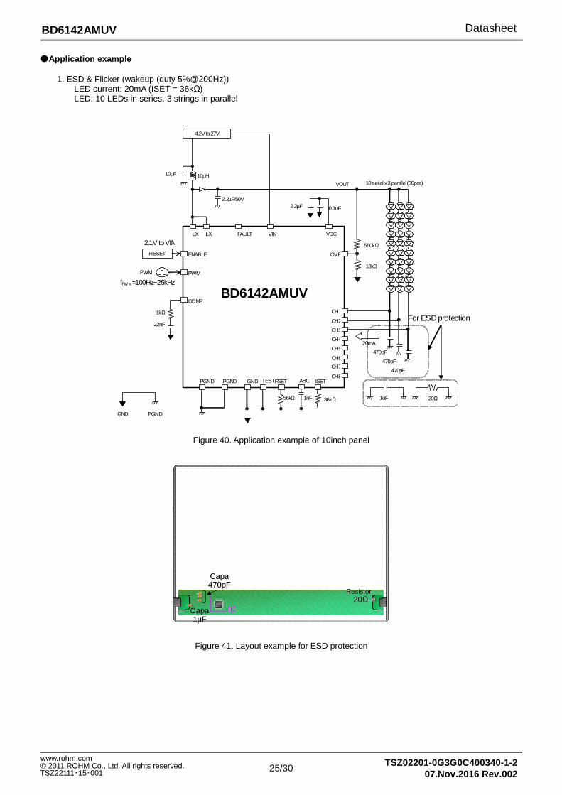
Application example
1. ESD & Flicker (wakeup (duty 5%@200Hz)) LED current: 20mA (ISET = 36kΩ) LED: 10 LEDs in series, 3 strings in parallel
Figure 40. Application example of 10inch panel
D 6 1 4 2
CCaappaa 447700ppFF
RReessiissttoorr 2200ΩΩ
IICC CCaappaa 11µµFF
Figure 41. Layout example for ESD protection
BD6142AMUV CH1
CH2
CH3
CH4
CH5
CH6
CH7
CH8
OVP
10 serial x 3 parallel (30pcs)
20mA
ABC
LX LX
2.2µF/50V
FAULT VIN
10µH 10µF
4.2V to 27V
ENABLE RESET
PWM
2.1V to VIN
COMP
1kΩ
ISET
36kΩ
GND PGND
PWM
fPWM=100Hz~25kHz
VDC
PGND
22nF
560kΩ
18kΩ
VOUT
2.2µF
GND PGND
FSET TEST
56kΩ 1nF
470pF
470pF
470pF
1uF 20Ω
For ESD protection
0.1uF

26/30
BD6142AMUV Datasheet
TSZ02201-0G3G0C400340-1-207.Nov.2016 Rev.002
www.rohm.com © 2011 ROHM Co., Ltd. All rights reserved. TSZ22111・15・001
2. Analog Dimming and monitoring FAULT terminal
LED current: 20mA (ISET = 36kΩ) LED: 10 LEDs in series, 8 strings in parallel
Figure 42. Application example of Analog dimming
3. Application example of CH terminal connected LED current: 20mA (ISET = 36kΩ) LED: 3LEDs ×12 strings
Figure 43. Application example of CH terminal connected
BD6142AMUV CH1
CH2
CH3
CH4
CH5
CH6
CH7
CH8
OVP
10 serial x 8 parallel (80pcs)
20mA ABC
LX LX
2.2µF/50V
FAULT VIN
10µH 10µF
7V to 27V
ENABLE RESET
PWM
2.1V to VIN
COMP
1kΩ
ISET
36kΩ
GND PGND
VDC
PGND
22nF
2.2MΩ
68kΩ
VOUT
2.2µF
GND PGND
FSET TEST
3V to 5V
monitor
D/A Max 0.9V
30kΩ
1nF
56kΩ
BD6142AMUV CH1 CH2 CH3 CH4 CH5 CH6 CH7 CH8
OVP
3 serial x 12parallel (36pcs)
30mA ABC
LX LX
2.2µF/50V
FAULT VIN
10µH 10µF
5V
ENABLE RESET
PWM
2.1V to VIN
COMP
1kΩ
ISET
24kΩ
GND PGND
VDC
PGND
22nF
2.2MΩ
160kΩ
VOUT
2.2µF
GND PGND
FSET TEST
3V to 5V
monitor 30kΩ
1nF
56kΩ
PWM

27/30
BD6142AMUV Datasheet
TSZ02201-0G3G0C400340-1-207.Nov.2016 Rev.002
www.rohm.com © 2011 ROHM Co., Ltd. All rights reserved. TSZ22111・15・001
Operational Notes (1) Absolute Maximum Ratings
An excess in the absolute maximum ratings, such as supply voltage, temperature range of operating conditions, etc., can break down devices, thus making impossible to identify breaking mode such as a short circuit or an open circuit. If any special mode exceeding the absolute maximum ratings is assumed, consideration should be given to take physical safety measures including the use of fuses, etc.
(2) Operating conditions These conditions represent a range within which characteristics can be provided approximately as expected. The electrical characteristics are guaranteed under the conditions of each parameter.
(3) Reverse connection of power supply connector The reverse connection of power supply connector can break down ICs. Take protective measures against the breakdown due to the reverse connection, such as mounting an external diode between the power supply and the IC’s power supply terminal.
(4) Power supply line Design PCB pattern to provide low impedance for the wiring between the power supply and the GND lines. In this regard, for the digital block power supply and the analog block power supply, even though these power supplies has the same level of potential, separate the power supply pattern for the digital block from that for the analog block, thus suppressing the diffraction of digital noises to the analog block power supply resulting from impedance common to the wiring patterns. For the GND line, give consideration to design the patterns in a similar manner. Furthermore, for all power supply terminals to ICs, mount a capacitor between the power supply and the GND terminal. At the same time, in order to use an electrolytic capacitor, thoroughly check to be sure the characteristics of the capacitor to be used present no problem including the occurrence of capacity dropout at a low temperature, thus determining the constant.
(5) GND voltage Make setting of the potential of the GND terminal so that it will be maintained at the minimum in any operating state. Furthermore, check to be sure no terminals are at a potential lower than the GND voltage including an actual electric transient.
(6) Short circuit between terminals and erroneous mounting In order to mount ICs on a set PCB, pay thorough attention to the direction and offset of the ICs. Erroneous mounting can break down the ICs. Furthermore, if a short circuit occurs due to foreign matters entering between terminals or between the terminal and the power supply or the GND terminal, the ICs can break down.
(7) Operation in strong electromagnetic field Be noted that using ICs in the strong electromagnetic field can malfunction them.
(8) Inspection with set PCB On the inspection with the set PCB, if a capacitor is connected to a low-impedance IC terminal, the IC can suffer stress. Therefore, be sure to discharge from the set PCB by each process. Furthermore, in order to mount or dismount the set PCB to/from the jig for the inspection process, be sure to turn OFF the power supply and then mount the set PCB to the jig. After the completion of the inspection, be sure to turn OFF the power supply and then dismount it from the jig. In addition, for protection against static electricity, establish a ground for the assembly process and pay thorough attention to the transportation and the storage of the set PCB.
(9) Input terminals In terms of the construction of IC, parasitic elements are inevitably formed in relation to potential. The operation of the parasitic element can cause interference with circuit operation, thus resulting in a malfunction and then breakdown of the input terminal. Therefore, pay thorough attention not to handle the input terminals, such as to apply to the input terminals a voltage lower than the GND respectively, so that any parasitic element will operate. Furthermore, do not apply a voltage to the input terminals when no power supply voltage is applied to the IC. In addition, even if the power supply voltage is applied, apply to the input terminals a voltage lower than the power supply voltage or within the guaranteed value of electrical characteristics.
(10) Ground wiring pattern If small-signal GND and large-current GND are provided, It will be recommended to separate the large-current GND pattern from the small-signal GND pattern and establish a single ground at the reference point of the set PCB so that resistance to the wiring pattern and voltage fluctuations due to a large current will cause no fluctuations in voltages of the small-signal GND. Pay attention not to cause fluctuations in the GND wiring pattern of external parts as well.
28/30
BD6142AMUV Datasheet
TSZ02201-0G3G0C400340-1-207.Nov.2016 Rev.002
www.rohm.com © 2011 ROHM Co., Ltd. All rights reserved. TSZ22111・15・001
(11) External capacitor In order to use a ceramic capacitor as the external capacitor, determine the constant with consideration given to a degradation in the nominal capacitance due to DC bias and changes in the capacitance due to temperature, etc.
(12) Thermal shutdown circuit (TSD) When junction temperatures become 130 (typ.) or higher, the thermal shutdown circuit operates and turns a switch OFF. The thermal shutdown circuit, which is aimed at isolating the LSI from thermal runaway as much as possible, is not aimed at the protection or guarantee of the LSI. Therefore, do not continuously use the LSI with this circuit operating or use the LSI assuming its operation.
(13) Thermal design Perform thermal design in which there are adequate margins by taking into account the permissible dissipation (Pd) in actual states of use.
(14) Selection of coil Select the low DCR inductors to decrease power loss for DC/DC converter.
Status of this document The Japanese version of this document is formal specification. A customer may use this translation version only for a reference to help reading the formal version. If there are any differences in translation version of this document formal version takes priority.
29/30
BD6142AMUV Datasheet
TSZ02201-0G3G0C400340-1-207.Nov.2016 Rev.002
www.rohm.com © 2011 ROHM Co., Ltd. All rights reserved. TSZ22111・15・001
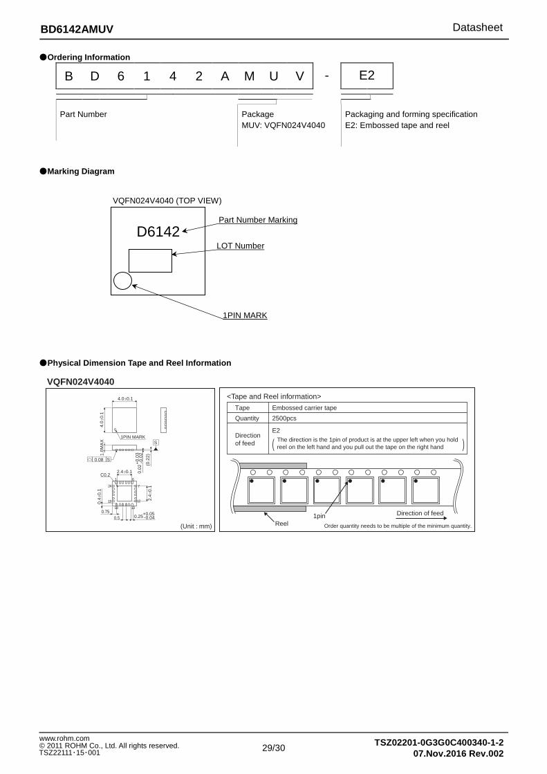
Ordering Information
B D 6 1 4 2 A M U V - E2
Part Number
Package MUV: VQFN024V4040
Packaging and forming specification E2: Embossed tape and reel
Marking Diagram Physical Dimension Tape and Reel Information
(Unit : mm)
VQFN024V4040
0.08 S
S
1 6
7
1219
24
1318
0.4±
0.1
0.02
+0.
03-0
.02
1PIN MARK
2.4±
0.1
C0.2
0.5
4.0±
0.1
0.75
2.4±0.1
4.0±0.1
1.0M
AX
(0.2
2)
0.25+0.05-0.04
∗ Order quantity needs to be multiple of the minimum quantity.
<Tape and Reel information>
Embossed carrier tapeTape
Quantity
Direction of feed
The direction is the 1pin of product is at the upper left when you hold reel on the left hand and you pull out the tape on the right hand
2500pcs
E2
( )
Direction of feed
Reel1pin
VQFN024V4040 (TOP VIEW)
1PIN MARK
Part Number Marking
LOT Number
D6142
30/30
BD6142AMUV Datasheet
TSZ02201-0G3G0C400340-1-207.Nov.2016 Rev.002
www.rohm.com © 2011 ROHM Co., Ltd. All rights reserved. TSZ22111・15・001
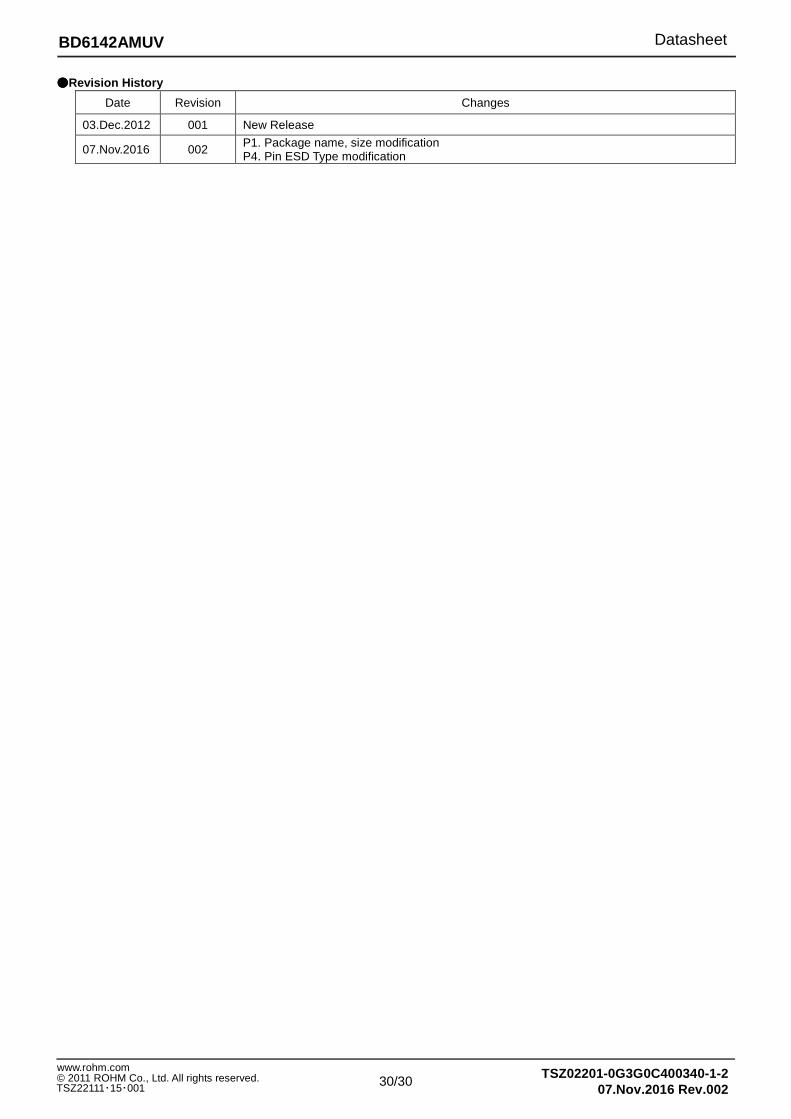
Revision History
Date Revision Changes
03.Dec.2012 001 New Release
07.Nov.2016 002 P1. Package name, size modification P4. Pin ESD Type modification

Notice-PGA-E Rev.003
© 2015 ROHM Co., Ltd. All rights reserved.
Notice
Precaution on using ROHM Products 1. Our Products are designed and manufactured for application in ordinary electronic equipments (such as AV equipment,
OA equipment, telecommunication equipment, home electronic appliances, amusement equipment, etc.). If you intend to use our Products in devices requiring extremely high reliability (such as medical equipment
(Note 1), transport
equipment, traffic equipment, aircraft/spacecraft, nuclear power controllers, fuel controllers, car equipment including car accessories, safety devices, etc.) and whose malfunction or failure may cause loss of human life, bodily injury or serious damage to property (“Specific Applications”), please consult with the ROHM sales representative in advance. Unless otherwise agreed in writing by ROHM in advance, ROHM shall not be in any way responsible or liable for any damages, expenses or losses incurred by you or third parties arising from the use of any ROHM’s Products for Specific Applications.
(Note1) Medical Equipment Classification of the Specific Applications
JAPAN USA EU CHINA
CLASSⅢ CLASSⅢ
CLASSⅡb CLASSⅢ
CLASSⅣ CLASSⅢ
2. ROHM designs and manufactures its Products subject to strict quality control system. However, semiconductor
products can fail or malfunction at a certain rate. Please be sure to implement, at your own responsibilities, adequate safety measures including but not limited to fail-safe design against the physical injury, damage to any property, which a failure or malfunction of our Products may cause. The following are examples of safety measures:
[a] Installation of protection circuits or other protective devices to improve system safety [b] Installation of redundant circuits to reduce the impact of single or multiple circuit failure
3. Our Products are designed and manufactured for use under standard conditions and not under any special or extraordinary environments or conditions, as exemplified below. Accordingly, ROHM shall not be in any way responsible or liable for any damages, expenses or losses arising from the use of any ROHM’s Products under any special or extraordinary environments or conditions. If you intend to use our Products under any special or extraordinary environments or conditions (as exemplified below), your independent verification and confirmation of product performance, reliability, etc, prior to use, must be necessary:
[a] Use of our Products in any types of liquid, including water, oils, chemicals, and organic solvents [b] Use of our Products outdoors or in places where the Products are exposed to direct sunlight or dust [c] Use of our Products in places where the Products are exposed to sea wind or corrosive gases, including Cl2,
H2S, NH3, SO2, and NO2
[d] Use of our Products in places where the Products are exposed to static electricity or electromagnetic waves [e] Use of our Products in proximity to heat-producing components, plastic cords, or other flammable items [f] Sealing or coating our Products with resin or other coating materials [g] Use of our Products without cleaning residue of flux (even if you use no-clean type fluxes, cleaning residue of
flux is recommended); or Washing our Products by using water or water-soluble cleaning agents for cleaning residue after soldering
[h] Use of the Products in places subject to dew condensation
4. The Products are not subject to radiation-proof design. 5. Please verify and confirm characteristics of the final or mounted products in using the Products. 6. In particular, if a transient load (a large amount of load applied in a short period of time, such as pulse. is applied,
confirmation of performance characteristics after on-board mounting is strongly recommended. Avoid applying power exceeding normal rated power; exceeding the power rating under steady-state loading condition may negatively affect product performance and reliability.
7. De-rate Power Dissipation depending on ambient temperature. When used in sealed area, confirm that it is the use in
the range that does not exceed the maximum junction temperature. 8. Confirm that operation temperature is within the specified range described in the product specification. 9. ROHM shall not be in any way responsible or liable for failure induced under deviant condition from what is defined in
this document.
Precaution for Mounting / Circuit board design 1. When a highly active halogenous (chlorine, bromine, etc.) flux is used, the residue of flux may negatively affect product
performance and reliability.
2. In principle, the reflow soldering method must be used on a surface-mount products, the flow soldering method must be used on a through hole mount products. If the flow soldering method is preferred on a surface-mount products, please consult with the ROHM representative in advance.
For details, please refer to ROHM Mounting specification

Notice-PGA-E Rev.003
© 2015 ROHM Co., Ltd. All rights reserved.
Precautions Regarding Application Examples and External Circuits 1. If change is made to the constant of an external circuit, please allow a sufficient margin considering variations of the
characteristics of the Products and external components, including transient characteristics, as well as static characteristics.
2. You agree that application notes, reference designs, and associated data and information contained in this document
are presented only as guidance for Products use. Therefore, in case you use such information, you are solely responsible for it and you must exercise your own independent verification and judgment in the use of such information contained in this document. ROHM shall not be in any way responsible or liable for any damages, expenses or losses incurred by you or third parties arising from the use of such information.
Precaution for Electrostatic This Product is electrostatic sensitive product, which may be damaged due to electrostatic discharge. Please take proper caution in your manufacturing process and storage so that voltage exceeding the Products maximum rating will not be applied to Products. Please take special care under dry condition (e.g. Grounding of human body / equipment / solder iron, isolation from charged objects, setting of Ionizer, friction prevention and temperature / humidity control).
Precaution for Storage / Transportation 1. Product performance and soldered connections may deteriorate if the Products are stored in the places where:
[a] the Products are exposed to sea winds or corrosive gases, including Cl2, H2S, NH3, SO2, and NO2 [b] the temperature or humidity exceeds those recommended by ROHM [c] the Products are exposed to direct sunshine or condensation [d] the Products are exposed to high Electrostatic
2. Even under ROHM recommended storage condition, solderability of products out of recommended storage time period may be degraded. It is strongly recommended to confirm solderability before using Products of which storage time is exceeding the recommended storage time period.
3. Store / transport cartons in the correct direction, which is indicated on a carton with a symbol. Otherwise bent leads
may occur due to excessive stress applied when dropping of a carton. 4. Use Products within the specified time after opening a humidity barrier bag. Baking is required before using Products of
which storage time is exceeding the recommended storage time period.
Precaution for Product Label A two-dimensional barcode printed on ROHM Products label is for ROHM’s internal use only.
Precaution for Disposition When disposing Products please dispose them properly using an authorized industry waste company.
Precaution for Foreign Exchange and Foreign Trade act Since concerned goods might be fallen under listed items of export control prescribed by Foreign exchange and Foreign trade act, please consult with ROHM in case of export.
Precaution Regarding Intellectual Property Rights 1. All information and data including but not limited to application example contained in this document is for reference
only. ROHM does not warrant that foregoing information or data will not infringe any intellectual property rights or any other rights of any third party regarding such information or data.
2. ROHM shall not have any obligations where the claims, actions or demands arising from the combination of the Products with other articles such as components, circuits, systems or external equipment (including software).
3. No license, expressly or implied, is granted hereby under any intellectual property rights or other rights of ROHM or any third parties with respect to the Products or the information contained in this document. Provided, however, that ROHM will not assert its intellectual property rights or other rights against you or your customers to the extent necessary to manufacture or sell products containing the Products, subject to the terms and conditions herein.
Other Precaution 1. This document may not be reprinted or reproduced, in whole or in part, without prior written consent of ROHM.
2. The Products may not be disassembled, converted, modified, reproduced or otherwise changed without prior written consent of ROHM.
3. In no event shall you use in any way whatsoever the Products and the related technical information contained in the Products or this document for any military purposes, including but not limited to, the development of mass-destruction weapons.
4. The proper names of companies or products described in this document are trademarks or registered trademarks of ROHM, its affiliated companies or third parties.

DatasheetDatasheet
Notice – WE Rev.001© 2015 ROHM Co., Ltd. All rights reserved.
General Precaution 1. Before you use our Pro ducts, you are requested to care fully read this document and fully understand its contents.
ROHM shall n ot be in an y way responsible or liabl e for fa ilure, malfunction or acci dent arising from the use of a ny ROHM’s Products against warning, caution or note contained in this document.
2. All information contained in this docume nt is current as of the issuing date and subj ect to change without any prior
notice. Before purchasing or using ROHM’s Products, please confirm the la test information with a ROHM sale s representative.
3. The information contained in this doc ument is provi ded on an “as is” basis and ROHM does not warrant that all
information contained in this document is accurate an d/or error-free. ROHM shall not be in an y way responsible or liable for any damages, expenses or losses incurred by you or third parties resulting from inaccuracy or errors of or concerning such information.
Related Documents