74LVC594A 8-bit shift register with output register Rev. 3 — 20 July 2017 Product data sheet 1 General description The 74LVC594A is an 8-bit serial-in/serial or parallel-out shift register with a storage register. Separate clock and reset inputs are provided on both shift and storage registers. The input can be driven from either 3.3 V or 5 V devices. This feature allows the use of this device in a mixed 3.3 V and 5 V environment. This device is fully specified for partial Power-down applications using I OFF . The I OFF circuitry disables the output, preventing the damaging backflow current through the device when it is powered down. The shift register has a serial input (DS) and a serial output (Q7S) for cascading purposes. Data is shifted on the positive-going transitions of the SHCP input. The data in the shift register is transferred to the storage register on a positive-going transition of the STCP input. If both clocks are connected together, the shift register will always be one clock pulse ahead of the storage register. A LOW level on one of the two register reset pins (SHR and STR ) will clear the corresponding register. 2 Features and benefits • 5 V tolerant inputs/outputs for interfacing with 5 V logic • Wide supply voltage range from 1.2 V to 3.6 V • CMOS low-power consumption • Direct interface with TTL levels • Balanced propagation delays • All inputs have Schmitt-trigger action • Complies with JEDEC standard: – JESD8-7A (1.65 V to 1.95 V) – JESD8-5A (2.3 V to 2.7 V) – JESD8-C/JESD36 (2.7 V to 3.6 V) • ESD protection: – HBM JESD22-A114F exceeds 2000 V – CDM JESD22-C101E exceeds 1000 V • Specified from -40 °C to +85 °C and -40 °C to +125 °C 3 Applications • Serial-to-parallel data conversion • Remote control holding register

Welcome message from author
This document is posted to help you gain knowledge. Please leave a comment to let me know what you think about it! Share it to your friends and learn new things together.
Transcript

74LVC594A8-bit shift register with output registerRev. 3 — 20 July 2017 Product data sheet
1 General description
The 74LVC594A is an 8-bit serial-in/serial or parallel-out shift register with a storageregister. Separate clock and reset inputs are provided on both shift and storage registers.
The input can be driven from either 3.3 V or 5 V devices. This feature allows the use ofthis device in a mixed 3.3 V and 5 V environment.
This device is fully specified for partial Power-down applications using IOFF. The IOFFcircuitry disables the output, preventing the damaging backflow current through thedevice when it is powered down.
The shift register has a serial input (DS) and a serial output (Q7S) for cascadingpurposes. Data is shifted on the positive-going transitions of the SHCP input. The data inthe shift register is transferred to the storage register on a positive-going transition of theSTCP input. If both clocks are connected together, the shift register will always be oneclock pulse ahead of the storage register. A LOW level on one of the two register resetpins (SHR and STR) will clear the corresponding register.
2 Features and benefits
• 5 V tolerant inputs/outputs for interfacing with 5 V logic• Wide supply voltage range from 1.2 V to 3.6 V• CMOS low-power consumption• Direct interface with TTL levels• Balanced propagation delays• All inputs have Schmitt-trigger action• Complies with JEDEC standard:
– JESD8-7A (1.65 V to 1.95 V)– JESD8-5A (2.3 V to 2.7 V)– JESD8-C/JESD36 (2.7 V to 3.6 V)
• ESD protection:– HBM JESD22-A114F exceeds 2000 V– CDM JESD22-C101E exceeds 1000 V
• Specified from -40 °C to +85 °C and -40 °C to +125 °C
3 Applications
• Serial-to-parallel data conversion• Remote control holding register
Nexperia 74LVC594A8-bit shift register with output register
74LVC594A All information provided in this document is subject to legal disclaimers. © Nexperia B.V. 2017. All rights reserved.
Product data sheet Rev. 3 — 20 July 20172 / 21
4 Ordering informationTable 1. Ordering information
PackageType number
Temperaturerange
Name Description Version
74LVC594AD -40 °C to +125 °C SO16 plastic small outline package; 16 leads;body width 3.9 mm
SOT109-1
74LVC594APW -40 °C to +125 °C TSSOP16 plastic thin shrink small outline package; 16 leads;body width 4.4 mm
SOT403-1
74LVC594ABQ -40 °C to +125 °C DHVQFN16 plastic dual in-line compatible thermal enhancedvery thin quad flat package; no leads;16 terminals; body 2.5 x 3.5 x 0.85 mm
SOT763-1
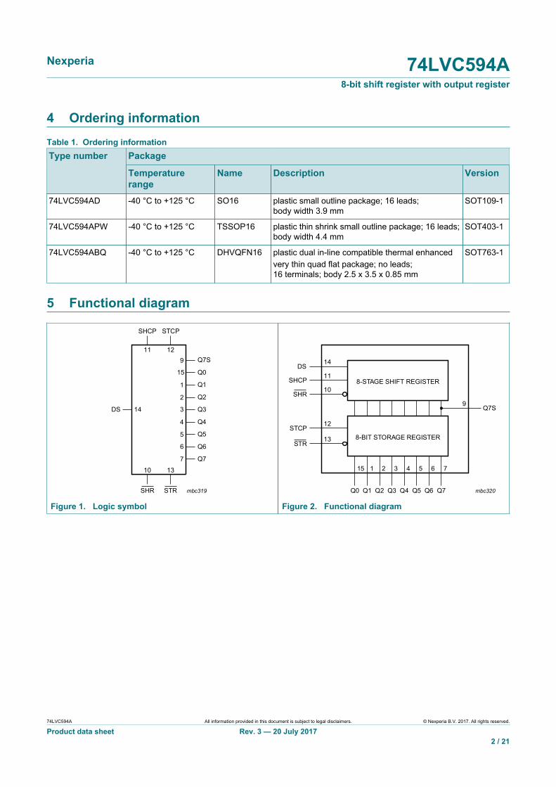
5 Functional diagram
mbc319
STCPSHCP
STRSHR
DS
Q7S
Q0
Q1
Q2
Q3
Q4
Q5
Q6
Q7
14
10 13
11 12
15
9
1
2
3
4
5
6
7
Figure 1. Logic symbol
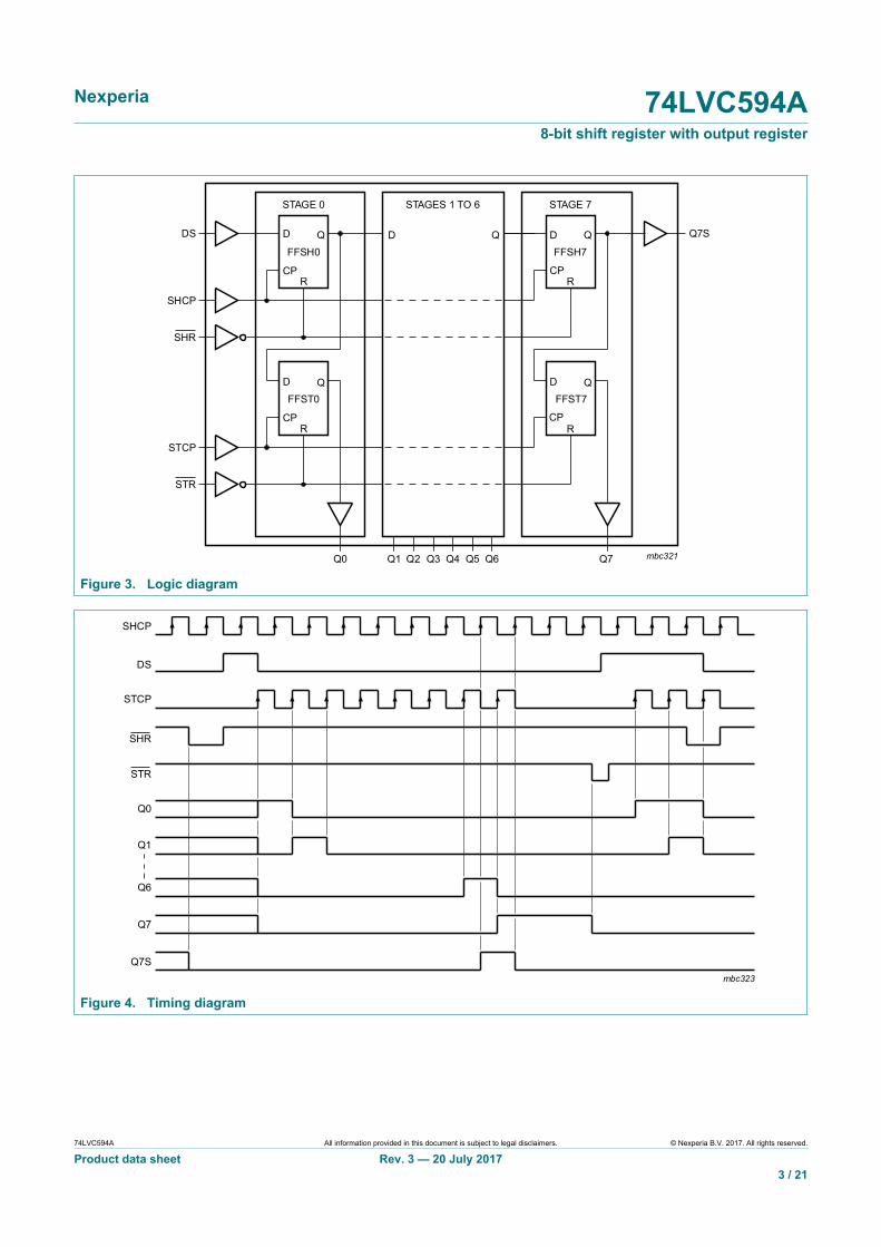
mbc320Q7Q0 Q1 Q2 Q3 Q4 Q5 Q6
DS
SHCP
SHR
STCP
STR
14
10
13
11
12
15
9
1 2 3 4 5 6 7
8-STAGE SHIFT REGISTER
8-BIT STORAGE REGISTER
Q7S
Figure 2. Functional diagram
Nexperia 74LVC594A8-bit shift register with output register
74LVC594A All information provided in this document is subject to legal disclaimers. © Nexperia B.V. 2017. All rights reserved.
Product data sheet Rev. 3 — 20 July 20173 / 21
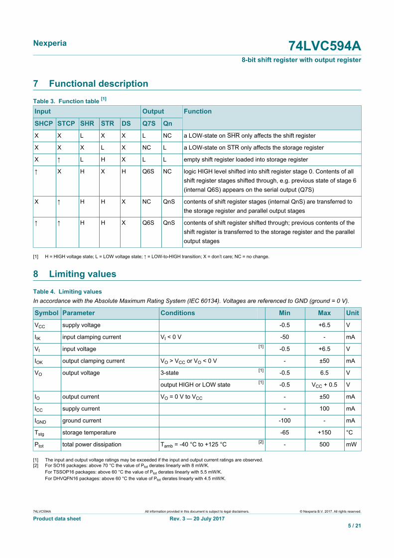
mbc321Q0 Q1 Q2 Q3 Q4 Q5 Q6
DS
SHCP
SHR
STCP
STR
D Q
CP
FFSH0
R
STAGE 0
D Q
CP
FFST0
R
STAGES 1 TO 6
D Q
Q7
D Q
CP
FFSH7
R
STAGE 7
D Q
CP
FFST7
R
Q7S
Figure 3. Logic diagram
mbc323
Q7S
Q0
STR
SHR
STCP
DS
SHCP
Q1
Q6
Q7
Figure 4. Timing diagram

Nexperia 74LVC594A8-bit shift register with output register
74LVC594A All information provided in this document is subject to legal disclaimers. © Nexperia B.V. 2017. All rights reserved.
Product data sheet Rev. 3 — 20 July 20174 / 21
6 Pinning information
6.1 Pinning
74LVC594A
Q1 VCC
Q2 Q0
Q3 DS
Q4 STR
Q5 STCP
Q6 SHCP
Q7 SHR
GND Q7S
001aag287
1
2
3
4
5
6
7
8
10
9
12
11
14
13
16
15
Figure 5. Pin configuration SO16 and TSSOP16
001aag288
74LVC594A
Q7 SHR
Q6 SHCP
Q5 STCP
Q4 STR
Q3 DS
Q2 Q0
GN
D
Q7S
Q1
VC
C
Transparent top view
7 10
6 11
5 12
4 13
3 14
2 15
8 9
1 16
terminal 1index area
Figure 6. Pin configuration DHVQFN16
6.2 Pin description
Table 2. Pin descriptionSymbol Pin Description
Q0, Q1, Q2, Q3, Q4, Q5, Q6, Q7 15, 1, 2, 3, 4, 5, 6, 7 parallel data output
GND 8 ground (0 V)
Q7S 9 serial data output
SHR 10 shift register reset (active LOW)
SHCP 11 shift register clock input
STCP 12 storage register clock input
STR 13 storage register reset (active LOW)
DS 14 serial data input
VCC 16 supply voltage
Nexperia 74LVC594A8-bit shift register with output register
74LVC594A All information provided in this document is subject to legal disclaimers. © Nexperia B.V. 2017. All rights reserved.
Product data sheet Rev. 3 — 20 July 20175 / 21
7 Functional description
Table 3. Function table [1]
Input Output
SHCP STCP SHR STR DS Q7S Qn
Function
X X L X X L NC a LOW-state on SHR only affects the shift register
X X X L X NC L a LOW-state on STR only affects the storage register
X ↑ L H X L L empty shift register loaded into storage register
↑ X H X H Q6S NC logic HIGH level shifted into shift register stage 0. Contents of allshift register stages shifted through, e.g. previous state of stage 6(internal Q6S) appears on the serial output (Q7S)
X ↑ H H X NC QnS contents of shift register stages (internal QnS) are transferred tothe storage register and parallel output stages
↑ ↑ H H X Q6S QnS contents of shift register shifted through; previous contents of theshift register is transferred to the storage register and the paralleloutput stages
[1] H = HIGH voltage state; L = LOW voltage state; ↑ = LOW-to-HIGH transition; X = don’t care; NC = no change.
8 Limiting values
Table 4. Limiting valuesIn accordance with the Absolute Maximum Rating System (IEC 60134). Voltages are referenced to GND (ground = 0 V).
Symbol Parameter Conditions Min Max Unit
VCC supply voltage -0.5 +6.5 V
IIK input clamping current VI < 0 V -50 - mA
VI input voltage [1] -0.5 +6.5 V
IOK output clamping current VO > VCC or VO < 0 V - ±50 mA
3-state [1] -0.5 6.5 VVO output voltage
output HIGH or LOW state [1] -0.5 VCC + 0.5 V
IO output current VO = 0 V to VCC - ±50 mA
ICC supply current - 100 mA
IGND ground current -100 - mA
Tstg storage temperature -65 +150 °C
Ptot total power dissipation Tamb = -40 °C to +125 °C [2] - 500 mW
[1] The input and output voltage ratings may be exceeded if the input and output current ratings are observed.[2] For SO16 packages: above 70 °C the value of Ptot derates linearly with 8 mW/K.
For TSSOP16 packages: above 60 °C the value of Ptot derates linearly with 5.5 mW/K.For DHVQFN16 packages: above 60 °C the value of Ptot derates linearly with 4.5 mW/K.
Nexperia 74LVC594A8-bit shift register with output register
74LVC594A All information provided in this document is subject to legal disclaimers. © Nexperia B.V. 2017. All rights reserved.
Product data sheet Rev. 3 — 20 July 20176 / 21
9 Recommended operating conditions
Table 5. Recommended operating conditionsSymbol Parameter Conditions Min Typ Max Unit
1.65 - 3.6 VVCC supply voltage
functional 1.2 - - V
VI input voltage 0 - 5.5 V
3-state 0 - 5.5 VVO output voltage
output HIGH or LOW state 0 - VCC V
Tamb ambient temperature -40 - +125 °C
VCC = 1.65 V to 2.7 V - - 20 ns/VΔt/ΔV input transition rise and fall rate
VCC = 2.7 V to 3.6 V - - 10 ns/V
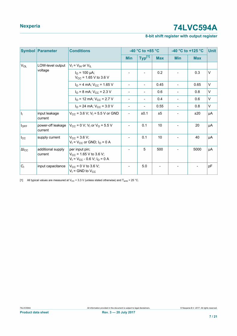
10 Static characteristics
Table 6. Static characteristicsAt recommended operating conditions. Voltages are referenced to GND (ground = 0 V).
-40 °C to +85 °C -40 °C to +125 °CSymbol Parameter Conditions
Min Typ[1] Max Min Max
Unit
VCC = 1.2 V 1.08 - - 1.08 - V
VCC = 1.65 V to 1.95 V 0.65VCC - - 0.65VCC - V
VCC = 2.3 V to 2.7 V 1.7 - - 1.7 - V
VIH HIGH-level inputvoltage
VCC = 2.7 V to 3.6 V 2.0 - - 2.0 - V
VCC = 1.2 V - - 0.12 - 0.12 V
VCC = 1.65 V to 1.95 V - - 0.35VCC - 0.35VCC V
VCC = 2.3 V to 2.7 V - - 0.7 - 0.7 V
VIL LOW-level inputvoltage
VCC = 2.7 V to 3.6 V - - 0.8 - 0.8 V
VI = VIH or VIL
IO = -100 μA;VCC = 1.65 V to 3.6 V
VCC-0.2 - - VCC-0.3 - V
IO = -4 mA; VCC = 1.65 V 1.2 - - 1.05 - V
IO = -8 mA; VCC = 2.3 V 1.8 - - 1.65 - V
IO = -12 mA; VCC = 2.7 V 2.2 - - 2.05 - V
IO = -18 mA; VCC = 3.0 V 2.4 - - 2.25 - V
VOH HIGH-level outputvoltage
IO = -24 mA; VCC = 3.0 V 2.2 - - 2.0 - V
Nexperia 74LVC594A8-bit shift register with output register
74LVC594A All information provided in this document is subject to legal disclaimers. © Nexperia B.V. 2017. All rights reserved.
Product data sheet Rev. 3 — 20 July 20177 / 21
-40 °C to +85 °C -40 °C to +125 °CSymbol Parameter Conditions
Min Typ[1] Max Min Max
Unit
VI = VIH or VIL
IO = 100 μA;VCC = 1.65 V to 3.6 V
- - 0.2 - 0.3 V
IO = 4 mA; VCC = 1.65 V - - 0.45 - 0.65 V
IO = 8 mA; VCC = 2.3 V - - 0.6 - 0.8 V
IO = 12 mA; VCC = 2.7 V - - 0.4 - 0.6 V
VOL LOW-level outputvoltage
IO = 24 mA; VCC = 3.0 V - - 0.55 - 0.8 V
II input leakagecurrent
VCC = 3.6 V; VI = 5.5 V or GND - ±0.1 ±5 - ±20 μA
IOFF power-off leakagecurrent
VCC = 0 V; VI or VO = 5.5 V - 0.1 10 - 20 μA
ICC supply current VCC = 3.6 V;VI = VCC or GND; IO = 0 A
- 0.1 10 - 40 μA
ΔICC additional supplycurrent
per input pin;VCC = 1.65 V to 3.6 V;VI = VCC - 0.6 V; IO = 0 A
- 5 500 - 5000 μA
CI input capacitance VCC = 0 V to 3.6 V;VI = GND to VCC
- 5.0 - - - pF
[1] All typical values are measured at VCC = 3.3 V (unless stated otherwise) and Tamb = 25 °C.
Nexperia 74LVC594A8-bit shift register with output register
74LVC594A All information provided in this document is subject to legal disclaimers. © Nexperia B.V. 2017. All rights reserved.
Product data sheet Rev. 3 — 20 July 20178 / 21
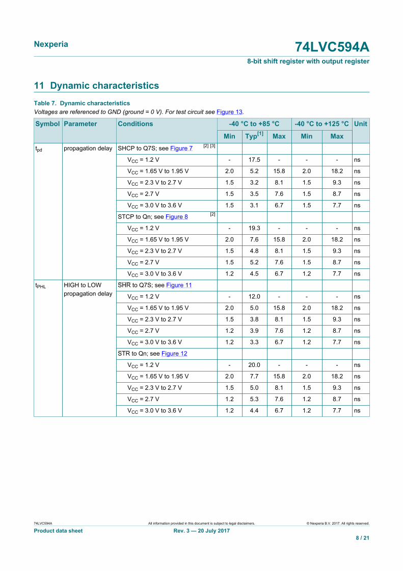
11 Dynamic characteristicsTable 7. Dynamic characteristicsVoltages are referenced to GND (ground = 0 V). For test circuit see Figure 13.
-40 °C to +85 °C -40 °C to +125 °CSymbol Parameter Conditions
Min Typ[1] Max Min Max
Unit
SHCP to Q7S; see Figure 7 [2] [3]
VCC = 1.2 V - 17.5 - - - ns
VCC = 1.65 V to 1.95 V 2.0 5.2 15.8 2.0 18.2 ns
VCC = 2.3 V to 2.7 V 1.5 3.2 8.1 1.5 9.3 ns
VCC = 2.7 V 1.5 3.5 7.6 1.5 8.7 ns
VCC = 3.0 V to 3.6 V 1.5 3.1 6.7 1.5 7.7 ns
STCP to Qn; see Figure 8 [2]
VCC = 1.2 V - 19.3 - - - ns
VCC = 1.65 V to 1.95 V 2.0 7.6 15.8 2.0 18.2 ns
VCC = 2.3 V to 2.7 V 1.5 4.8 8.1 1.5 9.3 ns
VCC = 2.7 V 1.5 5.2 7.6 1.5 8.7 ns
tpd propagation delay
VCC = 3.0 V to 3.6 V 1.2 4.5 6.7 1.2 7.7 ns
SHR to Q7S; see Figure 11
VCC = 1.2 V - 12.0 - - - ns
VCC = 1.65 V to 1.95 V 2.0 5.0 15.8 2.0 18.2 ns
VCC = 2.3 V to 2.7 V 1.5 3.8 8.1 1.5 9.3 ns
VCC = 2.7 V 1.2 3.9 7.6 1.2 8.7 ns
VCC = 3.0 V to 3.6 V 1.2 3.3 6.7 1.2 7.7 ns
STR to Qn; see Figure 12
VCC = 1.2 V - 20.0 - - - ns
VCC = 1.65 V to 1.95 V 2.0 7.7 15.8 2.0 18.2 ns
VCC = 2.3 V to 2.7 V 1.5 5.0 8.1 1.5 9.3 ns
VCC = 2.7 V 1.2 5.3 7.6 1.2 8.7 ns
tPHL HIGH to LOWpropagation delay
VCC = 3.0 V to 3.6 V 1.2 4.4 6.7 1.2 7.7 ns

Nexperia 74LVC594A8-bit shift register with output register
74LVC594A All information provided in this document is subject to legal disclaimers. © Nexperia B.V. 2017. All rights reserved.
Product data sheet Rev. 3 — 20 July 20179 / 21
-40 °C to +85 °C -40 °C to +125 °CSymbol Parameter Conditions
Min Typ[1] Max Min Max
Unit
SHCP, STCP HIGH or LOW;see Figure 7 and Figure 8
VCC = 1.65 V to 1.95 V 6.0 2.5 - 7.0 - ns
VCC = 2.3 V to 2.7 V 5.0 2.0 - 5.5 - ns
VCC = 2.7 V 4.5 1.5 - 5.0 - ns
VCC = 3.0 V to 3.6 V 4.0 1.5 - 4.5 - ns
SHR, STR LOW;see Figure 11 and Figure 12
VCC = 1.65 V to 1.95 V 6.0 2.5 - 5.5 - ns
VCC = 2.3 V to 2.7 V 4.0 2.0 - 4.5 - ns
VCC = 2.7 V 2.5 1.5 - 3.0 - ns
tW pulse width
VCC = 3.0 V to 3.6 V 2.5 1.5 - 3.0 - ns
DS to SHCP; see Figure 9
VCC = 1.65 V to 1.95 V 5.0 1.0 - 5.5 - ns
VCC = 2.3 V to 2.7 V 4.0 0.8 - 4.5 - ns
VCC = 2.7 V 2.0 0.6 - 2.5 - ns
VCC = 3.0 V to 3.6 V 2.0 0.6 - 2.5 - ns
SHR to STCP; see Figure 10
VCC = 1.65 V to 1.95 V 8.0 3.5 - 8.5 - ns
VCC = 2.3 V to 2.7 V 5.0 2.1 - 5.5 - ns
VCC = 2.7 V 4.0 1.8 - 4.5 - ns
VCC = 3.0 V to 3.6 V 4.0 1.7 - 4.5 - ns
SHCP to STCP; see Figure 8
VCC = 1.65 V to 1.95 V 8.0 3.5 - 8.5 - ns
VCC = 2.3 V to 2.7 V 5.0 2.1 - 5.5 - ns
VCC = 2.7 V 4.0 1.8 - 4.5 - ns
tsu set-up time
VCC = 3.0 V to 3.6 V 4.0 1.7 - 4.5 - ns
DS to SHCP; see Figure 9 [3]
VCC = 1.65 V to 1.95 V 1.5 0.2 - 2.0 - ns
VCC = 2.3 V to 2.7 V 1.5 0.1 - 2.0 - ns
VCC = 2.7 V 1.5 -0.1 - 2.0 - ns
th hold time
VCC = 3.0 V to 3.6 V 1.0 -0.2 - 1.5 - ns
Nexperia 74LVC594A8-bit shift register with output register
74LVC594A All information provided in this document is subject to legal disclaimers. © Nexperia B.V. 2017. All rights reserved.
Product data sheet Rev. 3 — 20 July 201710 / 21
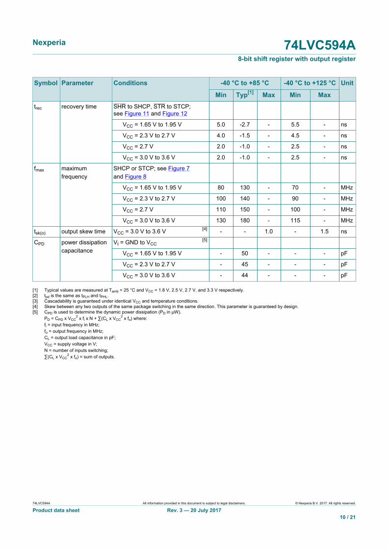
-40 °C to +85 °C -40 °C to +125 °CSymbol Parameter Conditions
Min Typ[1] Max Min Max
Unit
SHR to SHCP, STR to STCP;see Figure 11 and Figure 12
VCC = 1.65 V to 1.95 V 5.0 -2.7 - 5.5 - ns
VCC = 2.3 V to 2.7 V 4.0 -1.5 - 4.5 - ns
VCC = 2.7 V 2.0 -1.0 - 2.5 - ns
trec recovery time
VCC = 3.0 V to 3.6 V 2.0 -1.0 - 2.5 - ns
SHCP or STCP; see Figure 7and Figure 8
VCC = 1.65 V to 1.95 V 80 130 - 70 - MHz
VCC = 2.3 V to 2.7 V 100 140 - 90 - MHz
VCC = 2.7 V 110 150 - 100 - MHz
fmax maximumfrequency
VCC = 3.0 V to 3.6 V 130 180 - 115 - MHz
tsk(o) output skew time VCC = 3.0 V to 3.6 V [4] - - 1.0 - 1.5 ns
VI = GND to VCC[5]
VCC = 1.65 V to 1.95 V - 50 - - - pF
VCC = 2.3 V to 2.7 V - 45 - - - pF
CPD power dissipationcapacitance
VCC = 3.0 V to 3.6 V - 44 - - - pF
[1] Typical values are measured at Tamb = 25 °C and VCC = 1.8 V, 2.5 V, 2.7 V, and 3.3 V respectively.[2] tpd is the same as tPLH and tPHL.[3] Cascadability is guaranteed under identical VCC and temperature conditions.[4] Skew between any two outputs of the same package switching in the same direction. This parameter is guaranteed by design.[5] CPD is used to determine the dynamic power dissipation (PD in μW).
PD = CPD x VCC2 x fi x N + ∑(CL x VCC
2 x fo) where:fi = input frequency in MHz;fo = output frequency in MHz;CL = output load capacitance in pF;VCC = supply voltage in V;N = number of inputs switching;∑(CL x VCC
2 x fo) = sum of outputs.

Nexperia 74LVC594A8-bit shift register with output register
74LVC594A All information provided in this document is subject to legal disclaimers. © Nexperia B.V. 2017. All rights reserved.
Product data sheet Rev. 3 — 20 July 201711 / 21
11.1 Waveforms and test circuit
mna557
SHCP input
Q7S output
tPLH tPHL
tW
1/fmax
VM
VOH
VI
GND
VOL
VM
Measurement points are given in Table 8.VOL and VOH are typical output voltage drops that occur with the output load.
Figure 7. The shift clock (SHCP) to serial data output (Q7S) propagation delays, the shift clock pulse width andmaximum shift clock frequency
mna558
STCP input
Qn output
tPLH tPHL
tW
tsu 1/fmax
VM
VOH
VI
GND
VOL
VM
SHCP input
VI
GND
VM
Measurement points are given in Table 8.VOL and VOH are typical output voltage drops that occur with the output load.
Figure 8. The storage clock (STCP) to parallel data output (Qn) propagation delays, the storage clock pulse widthand the shift clock to storage clock set-up time
Nexperia 74LVC594A8-bit shift register with output register
74LVC594A All information provided in this document is subject to legal disclaimers. © Nexperia B.V. 2017. All rights reserved.
Product data sheet Rev. 3 — 20 July 201712 / 21
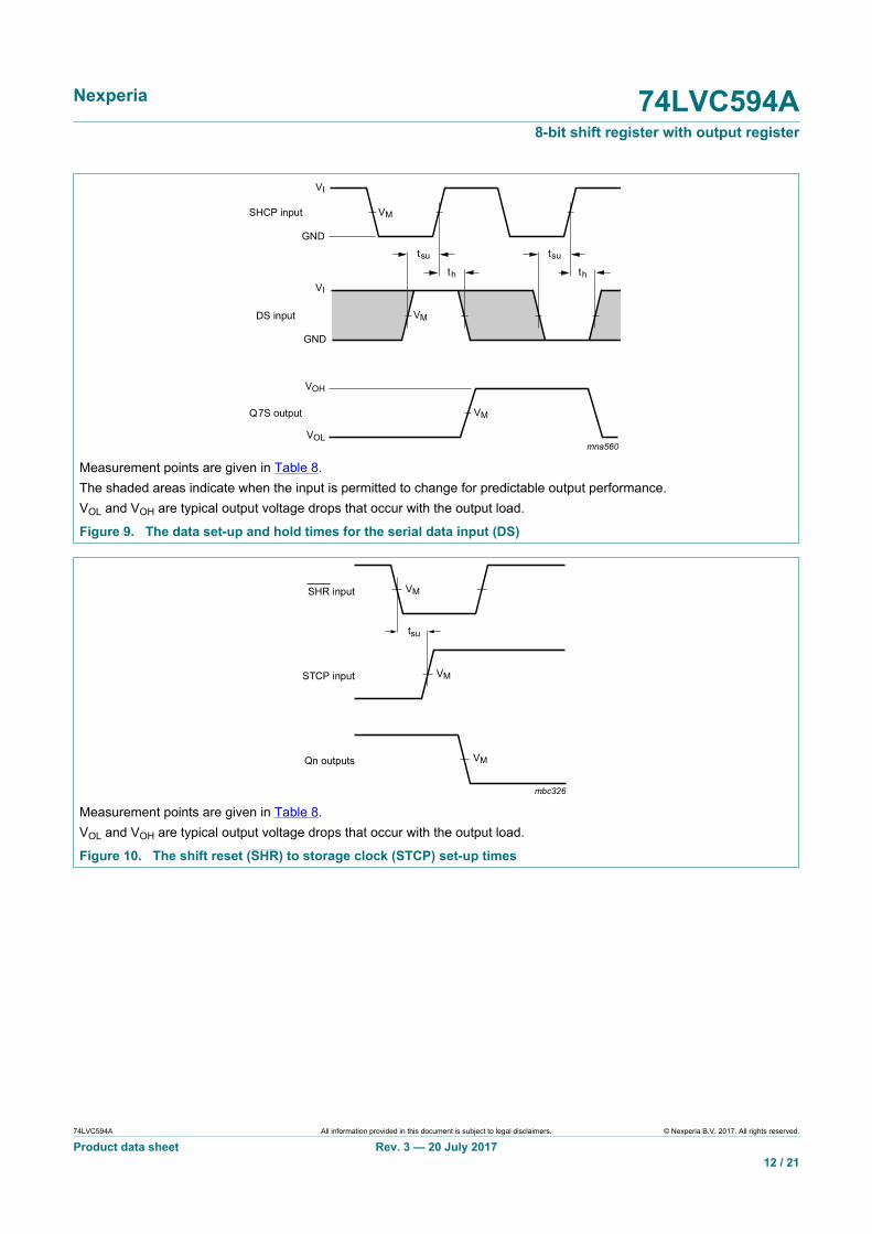
mna560
GND
GND
th
tsu
th
tsu
VM
VM
VM
VI
VOH
VOL
VI
Q7S output
SHCP input
DS input
Measurement points are given in Table 8.The shaded areas indicate when the input is permitted to change for predictable output performance.VOL and VOH are typical output voltage drops that occur with the output load.
Figure 9. The data set-up and hold times for the serial data input (DS)
mbc326
VM
tsu
VM
VM
STCP input
Qn outputs
SHR input
Measurement points are given in Table 8.VOL and VOH are typical output voltage drops that occur with the output load.
Figure 10. The shift reset (SHR) to storage clock (STCP) set-up times
Nexperia 74LVC594A8-bit shift register with output register
74LVC594A All information provided in this document is subject to legal disclaimers. © Nexperia B.V. 2017. All rights reserved.
Product data sheet Rev. 3 — 20 July 201713 / 21
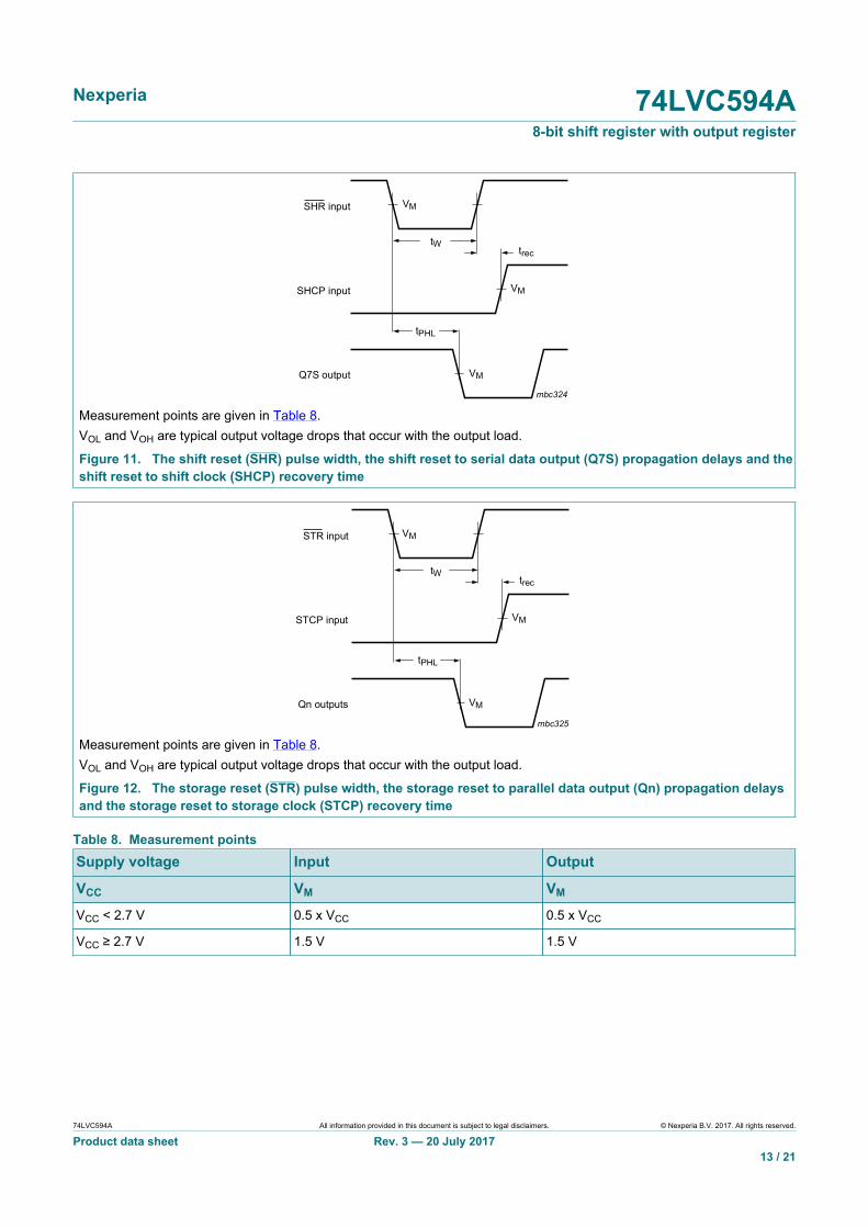
mbc324
VM
tPHL
VM
trectW
VM
SHCP input
Q7S output
SHR input
Measurement points are given in Table 8.VOL and VOH are typical output voltage drops that occur with the output load.
Figure 11. The shift reset (SHR) pulse width, the shift reset to serial data output (Q7S) propagation delays and theshift reset to shift clock (SHCP) recovery time
mbc325
VM
tPHL
VM
trectW
VM
STCP input
Qn outputs
STR input
Measurement points are given in Table 8.VOL and VOH are typical output voltage drops that occur with the output load.
Figure 12. The storage reset (STR) pulse width, the storage reset to parallel data output (Qn) propagation delaysand the storage reset to storage clock (STCP) recovery time
Table 8. Measurement pointsSupply voltage Input Output
VCC VM VM
VCC < 2.7 V 0.5 x VCC 0.5 x VCC
VCC ≥ 2.7 V 1.5 V 1.5 V
Nexperia 74LVC594A8-bit shift register with output register
74LVC594A All information provided in this document is subject to legal disclaimers. © Nexperia B.V. 2017. All rights reserved.
Product data sheet Rev. 3 — 20 July 201714 / 21
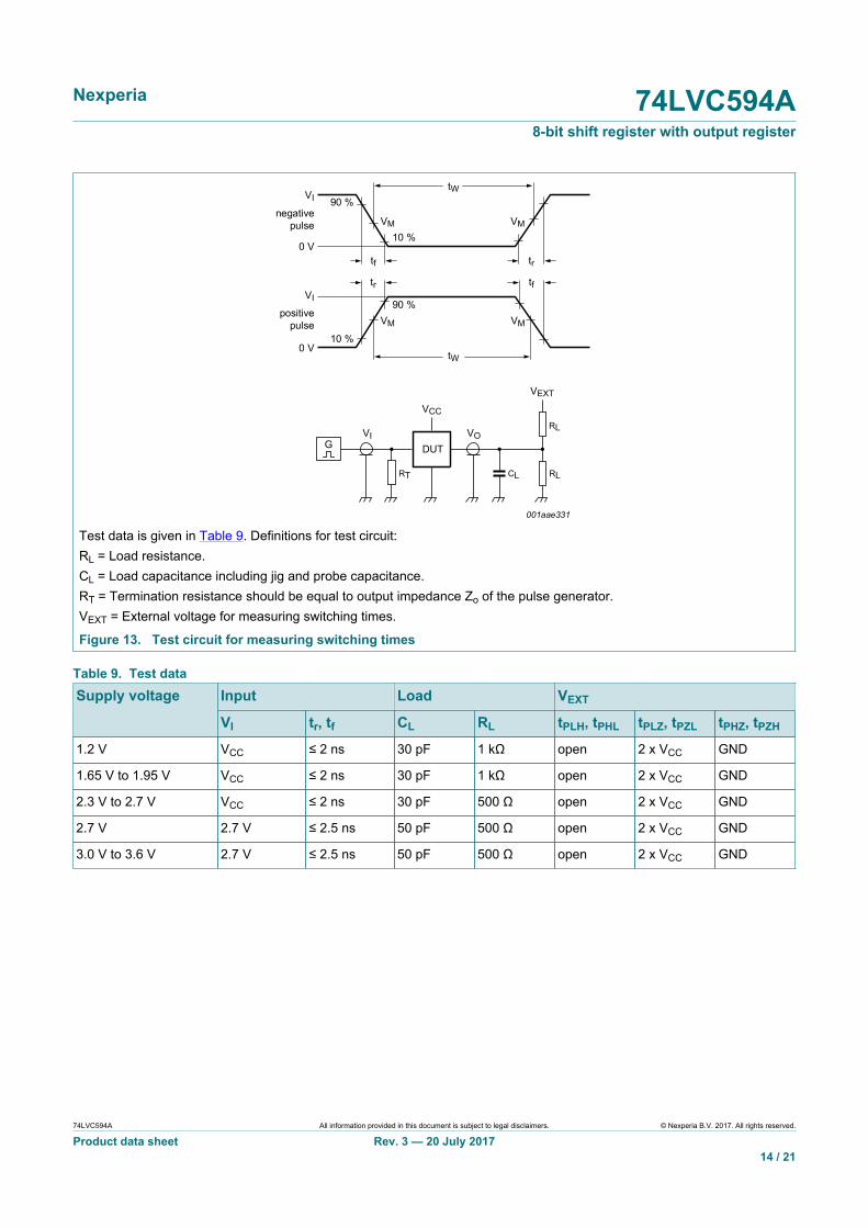
VM VM
tW
tW
10 %
90 %
0 V
VI
VI
negativepulse
positivepulse
0 V
VM VM
90 %
10 %
tf
tr
tr
tf
001aae331
VEXT
VCC
VI VODUT
CLRT
RL
RL
G
Test data is given in Table 9. Definitions for test circuit:RL = Load resistance.CL = Load capacitance including jig and probe capacitance.RT = Termination resistance should be equal to output impedance Zo of the pulse generator.VEXT = External voltage for measuring switching times.
Figure 13. Test circuit for measuring switching times
Table 9. Test dataInput Load VEXTSupply voltage
VI tr, tf CL RL tPLH, tPHL tPLZ, tPZL tPHZ, tPZH
1.2 V VCC ≤ 2 ns 30 pF 1 kΩ open 2 x VCC GND
1.65 V to 1.95 V VCC ≤ 2 ns 30 pF 1 kΩ open 2 x VCC GND
2.3 V to 2.7 V VCC ≤ 2 ns 30 pF 500 Ω open 2 x VCC GND
2.7 V 2.7 V ≤ 2.5 ns 50 pF 500 Ω open 2 x VCC GND
3.0 V to 3.6 V 2.7 V ≤ 2.5 ns 50 pF 500 Ω open 2 x VCC GND
Nexperia 74LVC594A8-bit shift register with output register
74LVC594A All information provided in this document is subject to legal disclaimers. © Nexperia B.V. 2017. All rights reserved.
Product data sheet Rev. 3 — 20 July 201715 / 21
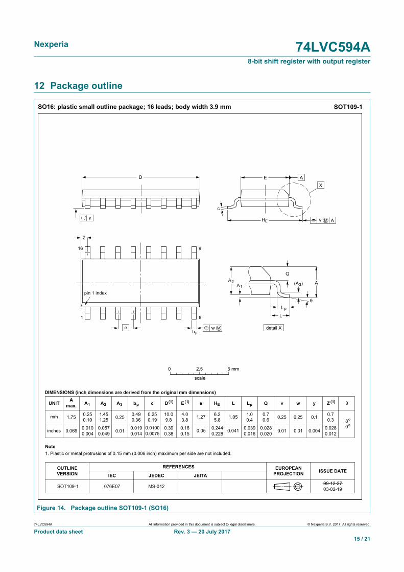
12 Package outline
X
w M
θ
AA1A2
bp
D
HE
Lp
Q
detail X
E
Z
e
c
L
v M A
(A )3
A
8
9
1
16
y
pin 1 index
UNITA
max. A1 A2 A3 bp c D(1) E (1) (1)e HE L Lp Q Zywv θ
REFERENCESOUTLINEVERSION
EUROPEANPROJECTION ISSUE DATE
IEC JEDEC JEITA
mm
inches
1.75 0.250.10
1.451.25 0.25 0.49
0.360.250.19
10.09.8
4.03.8 1.27 6.2
5.80.70.6
0.70.3 8
0
oo
0.25 0.1
DIMENSIONS (inch dimensions are derived from the original mm dimensions)
Note1. Plastic or metal protrusions of 0.15 mm (0.006 inch) maximum per side are not included.
1.00.4
SOT109-1 99-12-2703-02-19076E07 MS-012
0.069 0.0100.004
0.0570.049 0.01 0.019
0.0140.01000.0075
0.390.38
0.160.15 0.05
1.05
0.0410.2440.228
0.0280.020
0.0280.0120.01
0.25
0.01 0.0040.0390.016
0 2.5 5 mm
scale
SO16: plastic small outline package; 16 leads; body width 3.9 mm SOT109-1
Figure 14. Package outline SOT109-1 (SO16)
Nexperia 74LVC594A8-bit shift register with output register
74LVC594A All information provided in this document is subject to legal disclaimers. © Nexperia B.V. 2017. All rights reserved.
Product data sheet Rev. 3 — 20 July 201716 / 21
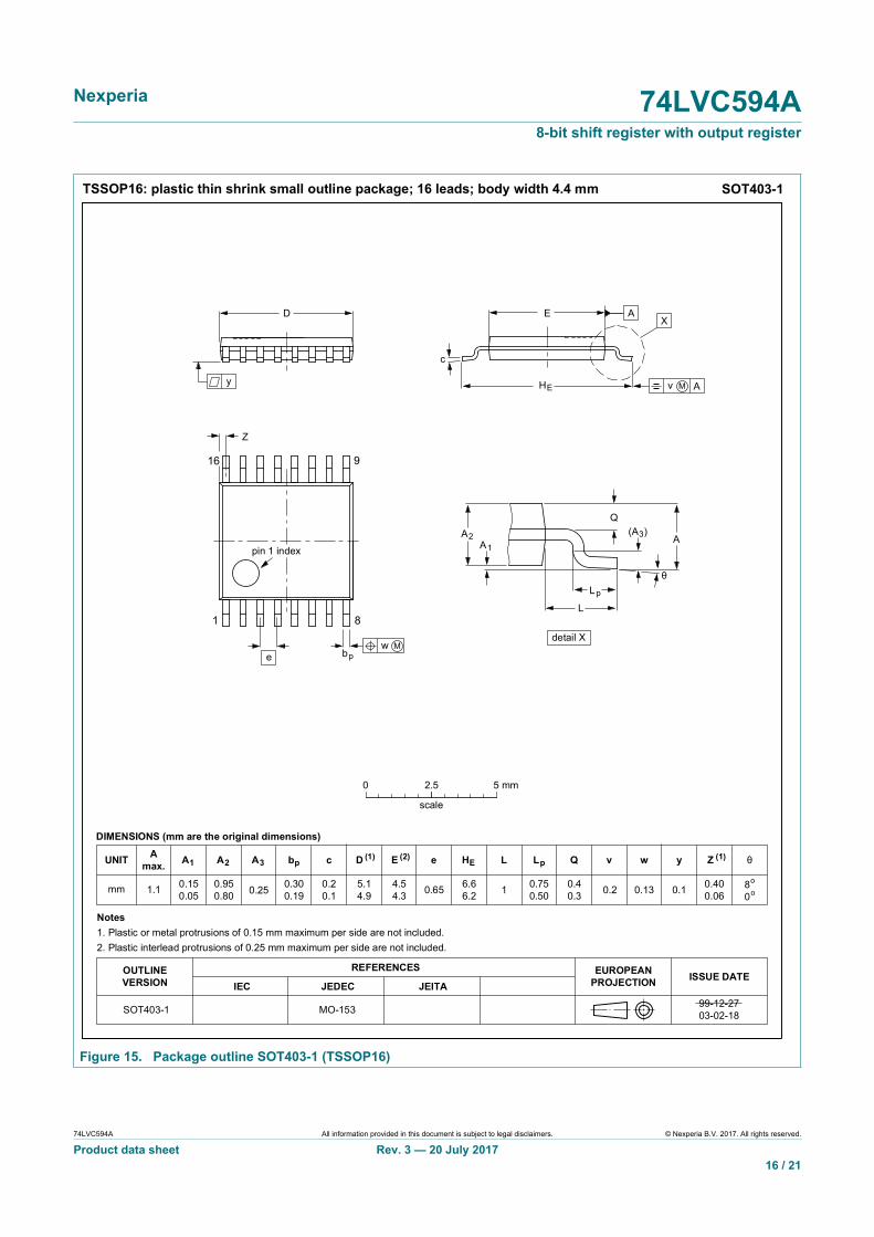
UNIT A1 A2 A3 bp c D (1) E (2) (1)e HE L Lp Q Zywv θ
REFERENCESOUTLINEVERSION
EUROPEANPROJECTION ISSUE DATE
IEC JEDEC JEITA
mm 0.150.05
0.950.80
0.300.19
0.20.1
5.14.9
4.54.3 0.65 6.6
6.20.40.3
0.400.06
80
oo0.13 0.10.21
DIMENSIONS (mm are the original dimensions)
Notes1. Plastic or metal protrusions of 0.15 mm maximum per side are not included.2. Plastic interlead protrusions of 0.25 mm maximum per side are not included.
0.750.50
SOT403-1 MO-153 99-12-2703-02-18
w Mbp
D
Z
e
0.25
1 8
16 9
θ
AA1A2
Lp
Q
detail X
L
(A )3
HE
E
c
v M A
XA
y
0 2.5 5 mm
scale
TSSOP16: plastic thin shrink small outline package; 16 leads; body width 4.4 mm SOT403-1
Amax.
1.1
pin 1 index
Figure 15. Package outline SOT403-1 (TSSOP16)

Nexperia 74LVC594A8-bit shift register with output register
74LVC594A All information provided in this document is subject to legal disclaimers. © Nexperia B.V. 2017. All rights reserved.
Product data sheet Rev. 3 — 20 July 201717 / 21
terminal 1index area
0.51
A1 EhbUNIT ye
0.2
c
REFERENCESOUTLINEVERSION
EUROPEANPROJECTION ISSUE DATE
IEC JEDEC JEITA
mm 3.63.4
Dh
2.151.85
y1
2.62.4
1.150.85
e1
2.50.300.18
0.050.00 0.05 0.1
DIMENSIONS (mm are the original dimensions)
SOT763-1 MO-241 - - -- - -
0.50.3
L
0.1
v
0.05
w
0 2.5 5 mm
scale
SOT763-1DHVQFN16: plastic dual in-line compatible thermal enhanced very thin quad flat package; no leads;16 terminals; body 2.5 x 3.5 x 0.85 mm
A(1)
max.
AA1
c
detail X
yy1 Ce
L
Eh
Dh
e
e1
b
2 7
15 10
9
81
16
X
D
E
C
B A
terminal 1index area
ACC
Bv M
w M
E(1)
Note1. Plastic or metal protrusions of 0.075 mm maximum per side are not included.
D(1)
02-10-1703-01-27
Figure 16. Package outline SOT763-1 (DHVQFN16)
Nexperia 74LVC594A8-bit shift register with output register
74LVC594A All information provided in this document is subject to legal disclaimers. © Nexperia B.V. 2017. All rights reserved.
Product data sheet Rev. 3 — 20 July 201718 / 21
13 AbbreviationsTable 10. AbbreviationsAcronym DescriptionCDM Charged Device Model
CMOS Complementary Metal Oxide Semiconductor
DUT Device Under Test
ESD ElectroStatic Discharge
HBM Human Body Model
TTL Transistor-Transistor Logic
14 Revision historyTable 11. Revision historyDocument ID Release date Data sheet status Change notice Supersedes74LVC594A v.3 20170720 Product data sheet - 74LVC594A v.2
Modifications: • The format of this data sheet has been redesigned to comply with the identity guidelines ofNexperia.
• Legal texts have been adapted to the new company name where appropriate.• Table 7: table note added for cascading purposes.
74LVC594A v.2 20131021 Product data sheet - 74LVC594A v.1
Modifications: • The format of this data sheet has been redesigned to comply with the new identityguidelines of NXP Semiconductors.
• Legal texts have been adapted to the new company name where appropriate.
74LVC594A v.1 20070524 Product data sheet - -
Nexperia 74LVC594A8-bit shift register with output register
74LVC594A All information provided in this document is subject to legal disclaimers. © Nexperia B.V. 2017. All rights reserved.
Product data sheet Rev. 3 — 20 July 201719 / 21
15 Legal information
15.1 Data sheet status
Document status[1][2] Product status[3] Definition
Objective [short] data sheet Development This document contains data from the objective specification for productdevelopment.
Preliminary [short] data sheet Qualification This document contains data from the preliminary specification.
Product [short] data sheet Production This document contains the product specification.
[1] Please consult the most recently issued document before initiating or completing a design.[2] The term 'short data sheet' is explained in section "Definitions".[3] The product status of device(s) described in this document may have changed since this document was published and may differ in case of multiple
devices. The latest product status information is available on the Internet at URL http://www.nexperia.com.
15.2 DefinitionsDraft — The document is a draft version only. The content is still underinternal review and subject to formal approval, which may result inmodifications or additions. Nexperia does not give any representations orwarranties as to the accuracy or completeness of information included hereinand shall have no liability for the consequences of use of such information.
Short data sheet — A short data sheet is an extract from a full data sheetwith the same product type number(s) and title. A short data sheet isintended for quick reference only and should not be relied upon to containdetailed and full information. For detailed and full information see therelevant full data sheet, which is available on request via the local Nexperiasales office. In case of any inconsistency or conflict with the short data sheet,the full data sheet shall prevail.
Product specification — The information and data provided in a Productdata sheet shall define the specification of the product as agreed betweenNexperia and its customer, unless Nexperia and customer have explicitlyagreed otherwise in writing. In no event however, shall an agreement bevalid in which the Nexperia product is deemed to offer functions and qualitiesbeyond those described in the Product data sheet.
15.3 DisclaimersLimited warranty and liability — Information in this document is believedto be accurate and reliable. However, Nexperia does not give anyrepresentations or warranties, expressed or implied, as to the accuracyor completeness of such information and shall have no liability for theconsequences of use of such information. Nexperia takes no responsibilityfor the content in this document if provided by an information source outsideof Nexperia. In no event shall Nexperia be liable for any indirect, incidental,punitive, special or consequential damages (including - without limitation -lost profits, lost savings, business interruption, costs related to the removalor replacement of any products or rework charges) whether or not suchdamages are based on tort (including negligence), warranty, breach ofcontract or any other legal theory. Notwithstanding any damages thatcustomer might incur for any reason whatsoever, Nexperia's aggregate andcumulative liability towards customer for the products described herein shallbe limited in accordance with the Terms and conditions of commercial sale ofNexperia.
Right to make changes — Nexperia reserves the right to make changesto information published in this document, including without limitationspecifications and product descriptions, at any time and without notice. Thisdocument supersedes and replaces all information supplied prior to thepublication hereof.
Suitability for use — Nexperia products are not designed, authorized orwarranted to be suitable for use in life support, life-critical or safety-critical
systems or equipment, nor in applications where failure or malfunctionof an Nexperia product can reasonably be expected to result in personalinjury, death or severe property or environmental damage. Nexperia and itssuppliers accept no liability for inclusion and/or use of Nexperia products insuch equipment or applications and therefore such inclusion and/or use is atthe customer’s own risk.
Applications — Applications that are described herein for any of theseproducts are for illustrative purposes only. Nexperia makes no representationor warranty that such applications will be suitable for the specified usewithout further testing or modification. Customers are responsible for thedesign and operation of their applications and products using Nexperiaproducts, and Nexperia accepts no liability for any assistance withapplications or customer product design. It is customer’s sole responsibilityto determine whether the Nexperia product is suitable and fit for thecustomer’s applications and products planned, as well as for the plannedapplication and use of customer’s third party customer(s). Customers shouldprovide appropriate design and operating safeguards to minimize the risksassociated with their applications and products. Nexperia does not acceptany liability related to any default, damage, costs or problem which is basedon any weakness or default in the customer’s applications or products, orthe application or use by customer’s third party customer(s). Customer isresponsible for doing all necessary testing for the customer’s applicationsand products using Nexperia products in order to avoid a default of theapplications and the products or of the application or use by customer’s thirdparty customer(s). Nexperia does not accept any liability in this respect.
Limiting values — Stress above one or more limiting values (as defined inthe Absolute Maximum Ratings System of IEC 60134) will cause permanentdamage to the device. Limiting values are stress ratings only and (proper)operation of the device at these or any other conditions above thosegiven in the Recommended operating conditions section (if present) or theCharacteristics sections of this document is not warranted. Constant orrepeated exposure to limiting values will permanently and irreversibly affectthe quality and reliability of the device.
Terms and conditions of commercial sale — Nexperia products aresold subject to the general terms and conditions of commercial sale, aspublished at http://www.nexperia.com/profile/terms, unless otherwise agreedin a valid written individual agreement. In case an individual agreement isconcluded only the terms and conditions of the respective agreement shallapply. Nexperia hereby expressly objects to applying the customer’s generalterms and conditions with regard to the purchase of Nexperia products bycustomer.
No offer to sell or license — Nothing in this document may be interpretedor construed as an offer to sell products that is open for acceptance orthe grant, conveyance or implication of any license under any copyrights,patents or other industrial or intellectual property rights.
Export control — This document as well as the item(s) described hereinmay be subject to export control regulations. Export might require a priorauthorization from competent authorities.
Nexperia 74LVC594A8-bit shift register with output register
74LVC594A All information provided in this document is subject to legal disclaimers. © Nexperia B.V. 2017. All rights reserved.
Product data sheet Rev. 3 — 20 July 201720 / 21
Non-automotive qualified products — Unless this data sheet expresslystates that this specific Nexperia product is automotive qualified, theproduct is not suitable for automotive use. It is neither qualified nor tested inaccordance with automotive testing or application requirements. Nexperiaaccepts no liability for inclusion and/or use of non-automotive qualifiedproducts in automotive equipment or applications. In the event that customeruses the product for design-in and use in automotive applications toautomotive specifications and standards, customer (a) shall use the productwithout Nexperia's warranty of the product for such automotive applications,use and specifications, and (b) whenever customer uses the product forautomotive applications beyond Nexperia's specifications such use shall besolely at customer’s own risk, and (c) customer fully indemnifies Nexperiafor any liability, damages or failed product claims resulting from customer
design and use of the product for automotive applications beyond Nexperia'sstandard warranty and Nexperia's product specifications.
Translations — A non-English (translated) version of a document is forreference only. The English version shall prevail in case of any discrepancybetween the translated and English versions.
15.4 TrademarksNotice: All referenced brands, product names, service names andtrademarks are the property of their respective owners.
Nexperia 74LVC594A8-bit shift register with output register
Please be aware that important notices concerning this document and the product(s)described herein, have been included in section 'Legal information'.
© Nexperia B.V. 2017. All rights reserved.For more information, please visit: http://www.nexperia.comFor sales office addresses, please send an email to: [email protected]
Date of release: 20 July 2017Document identifier: 74LVC594A
Contents1 General description ............................................ 12 Features and benefits .........................................13 Applications .........................................................14 Ordering information .......................................... 25 Functional diagram ............................................. 26 Pinning information ............................................ 46.1 Pinning ...............................................................46.2 Pin description ................................................... 47 Functional description ........................................58 Limiting values ....................................................59 Recommended operating conditions ................ 610 Static characteristics .......................................... 611 Dynamic characteristics .....................................811.1 Waveforms and test circuit .............................. 1112 Package outline .................................................1513 Abbreviations .................................................... 1814 Revision history ................................................ 1815 Legal information ..............................................19
Related Documents


![hw6.ppt [호환 모드] - Yonsei Universitycsys.yonsei.ac.kr/lect/emhw/hw6-1.pdf · 연세대학교 컴퓨터정보통신 4 Shift Register 4-bit shift register clock의positive edge에서한자리씩shift](https://static.cupdf.com/doc/110x72/5e4b32780d9b5706db72a2fc/hw6ppt-eeoe-yonsei-eoee-e-4-shift-register.jpg)