74HC165; 74HCT165 8-bit parallel-in/serial out shift register Rev. 5 — 21 August 2017 Product data sheet 1 General description The 74HC165; 74HCT165 are 8-bit serial or parallel-in/serial-out shift registers. The device features a serial data input (DS), eight parallel data inputs (D0 to D7) and two complementary serial outputs (Q7 and Q7 ). When the parallel load input (PL ) is LOW the data from D0 to D7 is loaded into the shift register asynchronously. When PL is HIGH data enters the register serially at DS. When the clock enable input (CE ) is LOW data is shifted on the LOW-to-HIGH transitions of the CP input. A HIGH on CE will disable the CP input. Inputs are overvoltage tolerant to 15 V. This enables the device to be used in HIGH-to-LOW level shifting applications. 2 Features and benefits • Asynchronous 8-bit parallel load • Synchronous serial input • Complies with JEDEC standard no. 7A • Input levels: – For 74HC165: CMOS level – For 74HCT165: TTL level • ESD protection: – HBM JESD22-A114F exceeds 2000 V – MM JESD22-A115-A exceeds 200 V • Specified from -40 °C to +85 °C and from -40 °C to +125 °C 3 Applications • Parallel-to-serial data conversion

Welcome message from author
This document is posted to help you gain knowledge. Please leave a comment to let me know what you think about it! Share it to your friends and learn new things together.
Transcript
74HC165; 74HCT1658-bit parallel-in/serial out shift registerRev. 5 — 21 August 2017 Product data sheet
1 General description
The 74HC165; 74HCT165 are 8-bit serial or parallel-in/serial-out shift registers. Thedevice features a serial data input (DS), eight parallel data inputs (D0 to D7) and twocomplementary serial outputs (Q7 and Q7). When the parallel load input (PL) is LOW thedata from D0 to D7 is loaded into the shift register asynchronously. When PL is HIGHdata enters the register serially at DS. When the clock enable input (CE) is LOW data isshifted on the LOW-to-HIGH transitions of the CP input. A HIGH on CE will disable theCP input. Inputs are overvoltage tolerant to 15 V. This enables the device to be used inHIGH-to-LOW level shifting applications.
2 Features and benefits
• Asynchronous 8-bit parallel load• Synchronous serial input• Complies with JEDEC standard no. 7A• Input levels:
– For 74HC165: CMOS level– For 74HCT165: TTL level
• ESD protection:– HBM JESD22-A114F exceeds 2000 V– MM JESD22-A115-A exceeds 200 V
• Specified from -40 °C to +85 °C and from -40 °C to +125 °C
3 Applications
• Parallel-to-serial data conversion

Nexperia 74HC165; 74HCT1658-bit parallel-in/serial out shift register
74HC_HCT165 All information provided in this document is subject to legal disclaimers. © Nexperia B.V. 2017. All rights reserved.
Product data sheet Rev. 5 — 21 August 20172 / 22
4 Ordering informationTable 1. Ordering information
PackageType number
Temperaturerange
Name Description Version
74HC165D
74HCT165D
-40 °C to +125 °C SO16 plastic small outline package; 16 leads;body width 3.9 mm
SOT109-1
74HC165DB
74HCT165DB
-40 °C to +125 °C SSOP16 plastic shrink small outline package; 16 leads;body width 5.3 mm
SOT338-1
74HC165PW
74HCT165PW
-40 °C to +125 °C TSSOP16 plastic thin shrink small outline package; 16 leads;body width 4.4 mm
SOT403-1
74HC165BQ
74HCT165BQ
-40 °C to +125 °C DHVQFN16 plastic dual in-line compatible thermal enhancedvery thin quad flat package; no leads; 16 terminals;body 2.5 × 3.5 × 0.85 mm
SOT763-1
5 Functional diagram
mna985
D0
D1
D2
D3
D4
D5
D6
D7
CP CE
DS
Q7
Q7
10
152
7
9
6
PL1
5
4
3
14
13
12
11
Figure 1. Logic symbol
mna986
59
10
11
12
13
14
3
4
67
215
1
≥ 11 C3/
C2[LOAD]
G1[SHIFT]
3D
2D
2D
SRG8
Figure 2. IEC logic symbol

Nexperia 74HC165; 74HCT1658-bit parallel-in/serial out shift register
74HC_HCT165 All information provided in this document is subject to legal disclaimers. © Nexperia B.V. 2017. All rights reserved.
Product data sheet Rev. 5 — 21 August 20173 / 22
mna992
8-BIT SHIFT REGISTERPARALLEL-IN/SERIAL-OUT
9
7
PL
11
1
DS10
CP2Q7
D0 D1 D2 D3 D4 D5 D6 D7
Q7
12 13 14 3 4 5 6
CE15
Figure 3. Functional diagram
6 Pinning information
6.1 Pinning
74HC16574HCT165
PL VCC
CP CE
D4 D3
D5 D2
D6 D1
D7 D0
Q7 DS
GND Q7
001aah564
1
2
3
4
5
6
7
8
10
9
12
11
14
13
16
15
Figure 4. Pin configuration (SO16 and (T)SSOP16)
001aah565
74HC16574HCT165
Q7 DSGND(1)D7 D0
D6 D1
D5 D2
D4 D3
CP CEG
ND Q7
PL
VC
C
Transparent top view
7 10
6 11
5 12
4 13
3 14
2 158 9
1 16
terminal 1index area
(1) This is not a supply pin. The substrate is attachedto this pad using conductive die attach material. Thereis no electrical or mechanical requirement to solder thispad.However, if it is soldered, the solder land should remainfloating or be connected to GND.Figure 5. Pin configuration (DHVQFN16)

Nexperia 74HC165; 74HCT1658-bit parallel-in/serial out shift register
74HC_HCT165 All information provided in this document is subject to legal disclaimers. © Nexperia B.V. 2017. All rights reserved.
Product data sheet Rev. 5 — 21 August 20174 / 22
6.2 Pin description
Table 2. Pin descriptionSymbol Pin DescriptionPL 1 asynchronous parallel load input (active LOW)
CP 2 clock input (LOW-to-HIGH edge-triggered)
Q7 7 complementary output from the last stage
GND 8 ground (0 V)
Q7 9 serial output from the last stage
DS 10 serial data input
D0 to D7 11, 12, 13, 14, 3, 4, 5, 6 parallel data inputs (also referred to as Dn)
CE 15 clock enable input (active LOW)
VCC 16 positive supply voltage
7 Functional descriptionTable 3. Function table [1]
Inputs Qn registers OutputsOperating modes
PL CE CP DS D0 to D7 Q0 Q1 to Q6 Q7 Q7L X X X L L L to L L Hparallel load
L X X X H H H to H H L
H L ↑ l X L q0 to q5 q6 q6
H L ↑ h X H q0 to q5 q6 q6
H ↑ L l X L q0 to q5 q6 q6
serial shift
H ↑ L h X H q0 to q5 q6 q6
H H X X X q0 q1 to q6 q7 q7hold "do nothing"
H X H X X q0 q1 to q6 q7 q7
[1] H = HIGH voltage level;h = HIGH voltage level one set-up time prior to the LOW-to-HIGH clock transition;L = LOW voltage level;l = LOW voltage level one set-up time prior to the LOW-to-HIGH clock transition;q = state of the referenced output one set-up time prior to the LOW-to-HIGH clock transition;X = don’t care;↑ = LOW-to-HIGH clock transition.

Nexperia 74HC165; 74HCT1658-bit parallel-in/serial out shift register
74HC_HCT165 All information provided in this document is subject to legal disclaimers. © Nexperia B.V. 2017. All rights reserved.
Product data sheet Rev. 5 — 21 August 20175 / 22
CE
CP
DS
PL
D0
D1
D2
D3
D4
D5
D6
D7
Q7
Q7
mna993inhibit serial shift
load
Figure 6. Timing diagram
8 Limiting valuesTable 4. Limiting valuesIn accordance with the Absolute Maximum Rating System (IEC 60134). Voltages are referenced to GND (ground = 0 V)
Symbol Parameter Conditions Min Max UnitVCC supply voltage -0.5 +7 V
IIK input clamping current VI < -0.5 V or VI > VCC + 0.5 V [1] - ±20 mA
IOK output clamping current VO < -0.5 V or VO > VCC + 0.5 V [1] - ±20 mA
IO output current -0.5 V < VO < VCC + 0.5 V - ±25 mA
ICC supply current - 50 mA
IGND ground current -50 - mA
Tstg storage temperature -65 +150 °C
Ptot total power dissipation Tamb = -40 °C to +125 °C [2] - 500 mW
[1] The input and output voltage ratings may be exceeded if the input and output current ratings are observed.[2] For SO16 Packages: Ptot derates linearly with 8 mW/K above 70 °C.
For (T)SSOP16 Packages: Ptot derates linearly with 5.5 mW/K above 60 °C.For DHVQFN16 Packages: Ptot derates linearly with 4.5 mW/K above 60 °C.

Nexperia 74HC165; 74HCT1658-bit parallel-in/serial out shift register
74HC_HCT165 All information provided in this document is subject to legal disclaimers. © Nexperia B.V. 2017. All rights reserved.
Product data sheet Rev. 5 — 21 August 20176 / 22
9 Recommended operating conditionsTable 5. Recommended operating conditionsVoltages are referenced to GND (ground = 0 V)
74HC165 74HCT165Symbol Parameter Conditions
Min Typ Max Min Typ Max
Unit
VCC supply voltage 2.0 5.0 6.0 4.5 5.0 5.5 V
VI input voltage 0 - VCC 0 - VCC V
VO output voltage 0 - VCC 0 - VCC V
Tamb ambient temperature -40 - +125 -40 - +125 °C
VCC = 2.0 V - - 625 - - - ns/V
VCC = 4.5 V - 1.67 139 - 1.67 139 ns/V
Δt/ΔV input transition rise and fall rate
VCC = 6.0 V - - 83 - - - ns/V
10 Static characteristicsTable 6. Static characteristicsAt recommended operating conditions; voltages are referenced to GND (ground = 0 V).
25 °C -40 °C to+85 °C
-40 °C to+125 °C
Symbol Parameter Conditions
Min Typ Max Min Max Min Max
Unit
74HC165
VCC = 2.0 V 1.5 1.2 - 1.5 - 1.5 - V
VCC = 4.5 V 3.15 2.4 - 3.15 - 3.15 - V
VIH HIGH-level inputvoltage
VCC = 6.0 V 4.2 3.2 - 4.2 - 4.2 - V
VCC = 2.0 V - 0.8 0.5 - 0.5 - 0.5 V
VCC = 4.5 V - 2.1 1.35 - 1.35 - 1.35 V
VIL LOW-level inputvoltage
VCC = 6.0 V - 2.8 1.8 - 1.8 - 1.8 V
VI = VIH or VIL
IO = -20 μA; VCC = 2.0 V 1.9 2.0 - 1.9 - 1.9 - V
IO = -20 μA; VCC = 4.5 V 4.4 4.5 - 4.4 - 4.4 - V
IO = -20 μA; VCC = 6.0 V 5.9 6.0 - 5.9 - 5.9 - V
IO = -4.0 mA; VCC = 4.5 V 3.98 4.32 - 3.84 - 3.7 - V
VOH HIGH-leveloutput voltage
IO = -5.2 mA; VCC = 6.0 V 5.48 5.81 - 5.34 - 5.2 - V

Nexperia 74HC165; 74HCT1658-bit parallel-in/serial out shift register
74HC_HCT165 All information provided in this document is subject to legal disclaimers. © Nexperia B.V. 2017. All rights reserved.
Product data sheet Rev. 5 — 21 August 20177 / 22
25 °C -40 °C to+85 °C
-40 °C to+125 °C
Symbol Parameter Conditions
Min Typ Max Min Max Min Max
Unit
VI = VIH or VIL
IO = 20 μA; VCC = 2.0 V - 0 0.1 - 0.1 - 0.1 V
IO = 20 μA; VCC = 4.5 V - 0 0.1 - 0.1 - 0.1 V
IO = 20 μA; VCC = 6.0 V - 0 0.1 - 0.1 - 0.1 V
IO = 4.0 mA; VCC = 4.5 V - 0.15 0.26 - 0.33 - 0.4 V
VOL LOW-leveloutput voltage
IO = 5.2 mA; VCC = 6.0 V - 0.16 0.26 - 0.33 - 0.4 V
II input leakagecurrent
VI = VCC or GND; VCC = 6.0 V - - ±0.1 - ±1 - ±1 μA
ICC supply current VI = VCC or GND; IO = 0 A;VCC = 6.0 V
- - 8.0 - 80 - 160 μA
CI inputcapacitance
- 3.5 - - - - - pF
74HCT165
VIH HIGH-level inputvoltage
VCC = 4.5 V to 5.5 V 2.0 1.6 - 2.0 - 2.0 - V
VIL LOW-level inputvoltage
VCC = 4.5 V to 5.5 V - 1.2 0.8 - 0.8 - 0.8 V
VI = VIH or VIL; VCC = 4.5 V
IO = -20 μA 4.4 4.5 - 4.4 - 4.4 - V
VOH HIGH-leveloutput voltage
IO = -4.0 mA 3.98 4.32 - 3.84 - 3.7 - V
VI = VIH or VIL
IO = 20 μA; VCC = 4.5 V - 0 0.1 - 0.1 - 0.1 V
VOL LOW-leveloutput voltage
IO = 5.2 mA; VCC = 6.0 V - 0.16 0.26 - 0.33 - 0.4 V
II input leakagecurrent
VI = VCC or GND; VCC = 6.0 V - - ±0.1 - ±1 - ±1 μA
ICC supply current VI = VCC or GND; IO = 0 A;VCC = 6.0 V
- - 8.0 - 80 - 160 μA
per input pin; VI = VCC - 2.1 V;other inputs at VCC or GND;VCC = 4.5 V to 5.5 V
Dn and DS inputs - 35 126 - 157.5 - 171.5 μA
ΔICC additional supplycurrent
CP CE, and PL inputs - 65 234 - 292.5 - 318.5 μA
CI inputcapacitance
- 3.5 - - - - - pF
Nexperia 74HC165; 74HCT1658-bit parallel-in/serial out shift register
74HC_HCT165 All information provided in this document is subject to legal disclaimers. © Nexperia B.V. 2017. All rights reserved.
Product data sheet Rev. 5 — 21 August 20178 / 22
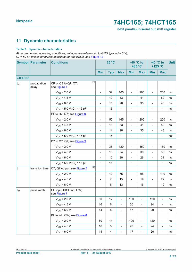
11 Dynamic characteristicsTable 7. Dynamic characteristicsAt recommended operating conditions; voltages are referenced to GND (ground = 0 V);CL = 50 pF unless otherwise specified; for test circuit, see Figure 12
25 °C -40 °C to+85 °C
-40 °C to+125 °C
Symbol Parameter Conditions
Min Typ Max Min Max Min Max
Unit
74HC165
CP or CE to Q7, Q7;see Figure 7
[1]
VCC = 2.0 V - 52 165 - 205 - 250 ns
VCC = 4.5 V - 19 33 - 41 - 50 ns
VCC = 6.0 V - 15 28 - 35 - 43 ns
VCC = 5.0 V; CL = 15 pF - 16 - - - - - ns
PL to Q7, Q7; see Figure 8
VCC = 2.0 V - 50 165 - 205 - 250 ns
VCC = 4.5 V - 18 33 - 41 - 50 ns
VCC = 6.0 V - 14 28 - 35 - 43 ns
VCC = 5.0 V; CL = 15 pF - 15 - - - - - ns
D7 to Q7, Q7; see Figure 9
VCC = 2.0 V - 36 120 - 150 - 180 ns
VCC = 4.5 V - 13 24 - 30 - 36 ns
VCC = 6.0 V - 10 20 - 26 - 31 ns
tpd propagationdelay
VCC = 5.0 V; CL = 15 pF - 11 - - - - - ns
Q7, Q7 output; see Figure 7 [2]
VCC = 2.0 V - 19 75 - 95 - 110 ns
VCC = 4.5 V - 7 15 - 19 - 22 ns
tt transition time
VCC = 6.0 V - 6 13 - 16 - 19 ns
CP input HIGH or LOW;see Figure 7
VCC = 2.0 V 80 17 - 100 - 120 - ns
VCC = 4.5 V 16 6 - 20 - 24 - ns
VCC = 6.0 V 14 5 - 17 - 20 - ns
PL input LOW; see Figure 8
VCC = 2.0 V 80 14 - 100 - 120 - ns
VCC = 4.5 V 16 5 - 20 - 24 - ns
tW pulse width
VCC = 6.0 V 14 4 - 17 - 20 - ns

Nexperia 74HC165; 74HCT1658-bit parallel-in/serial out shift register
74HC_HCT165 All information provided in this document is subject to legal disclaimers. © Nexperia B.V. 2017. All rights reserved.
Product data sheet Rev. 5 — 21 August 20179 / 22
25 °C -40 °C to+85 °C
-40 °C to+125 °C
Symbol Parameter Conditions
Min Typ Max Min Max Min Max
Unit
PL to CP, CE; see Figure 8
VCC = 2.0 V 100 22 - 125 - 150 - ns
VCC = 4.5 V 20 8 - 25 - 30 - ns
trec recovery time
VCC = 6.0 V 17 6 - 21 - 26 - ns
DS to CP, CE; see Figure 10
VCC = 2.0 V 80 11 - 100 - 120 - ns
VCC = 4.5 V 16 4 - 20 - 24 - ns
VCC = 6.0 V 14 3 - 17 - 20 - ns
CE to CP and CP to CE;see Figure 10
VCC = 2.0 V 80 17 - 100 - 120 - ns
VCC = 4.5 V 16 6 - 20 - 24 - ns
VCC = 6.0 V 14 5 - 17 - 20 - ns
Dn to PL; see Figure 11
VCC = 2.0 V 80 22 - 100 - 120 - ns
VCC = 4.5 V 16 8 - 20 - 24 - ns
tsu set-up time
VCC = 6.0 V 14 6 - 17 - 20 - ns
DS to CP, CE and Dn to PL;see Figure 10
VCC = 2.0 V 5 2 - 5 - 5 - ns
VCC = 4.5 V 5 2 - 5 - 5 - ns
VCC = 6.0 V 5 2 - 5 - 5 - ns
CE to CP and CP to CE;see Figure 10
VCC = 2.0 V 5 -17 - 5 - 5 - ns
VCC = 4.5 V 5 -6 - 5 - 5 - ns
th hold time
VCC = 6.0 V 5 -5 - 5 - 5 - ns
CP input; see Figure 7
VCC = 2.0 V 6 17 - 5 - 4 - MHz
VCC = 4.5 V 30 51 - 24 - 20 - MHz
VCC = 6.0 V 35 61 - 28 - 24 - MHz
fmax maximumfrequency
VCC = 5.0 V; CL = 15 pF - 56 - - - - - MHz
CPD powerdissipationcapacitance
per package; VI = GND to VCC[3] - 35 - - - - - pF

Nexperia 74HC165; 74HCT1658-bit parallel-in/serial out shift register
74HC_HCT165 All information provided in this document is subject to legal disclaimers. © Nexperia B.V. 2017. All rights reserved.
Product data sheet Rev. 5 — 21 August 201710 / 22
25 °C -40 °C to+85 °C
-40 °C to+125 °C
Symbol Parameter Conditions
Min Typ Max Min Max Min Max
Unit
74HCT165
CE, CP to Q7, Q7;see Figure 7
[1]
VCC = 4.5 V - 17 34 - 43 - 51 ns
VCC = 5.0 V; CL = 15 pF - 14 - - - - - ns
PL to Q7, Q7; see Figure 8
VCC = 4.5 V - 20 40 - 50 - 60 ns
VCC = 5.0 V; CL = 15 pF - 17 - - - - - ns
D7 to Q7, Q7; see Figure 9
VCC = 4.5 V - 14 28 - 35 - 42 ns
tpd propagationdelay
VCC = 5.0 V; CL = 15 pF - 11 - - - - - ns
Q7, Q7 output; see Figure 7 [2]tt transition time
VCC = 4.5 V - 7 15 - 19 - 22 ns
CP input; see Figure 7
VCC = 4.5 V 16 6 - 20 - 24 - ns
PL input; see Figure 8
tW pulse width
VCC = 4.5 V 20 9 - 25 - 30 - ns
PL to CP, CE; see Figure 8trec recovery time
VCC = 4.5 V 20 8 - 25 - 30 - ns
DS to CP, CE; see Figure 10
VCC = 4.5 V 20 2 - 25 - 30 - ns
CE to CP and CP to CE;see Figure 10
VCC = 4.5 V 20 7 - 25 - 30 - ns
Dn to PL; see Figure 11
tsu set-up time
VCC = 4.5 V 20 10 - 25 - 30 - ns
DS to CP, CE and Dn to PL;see Figure 10
VCC = 4.5 V 7 -1 - 9 - 11 - ns
CE to CP and CP to CE;see Figure 10
th hold time
VCC = 4.5 V 0 -7 - 0 - 0 - ns

Nexperia 74HC165; 74HCT1658-bit parallel-in/serial out shift register
74HC_HCT165 All information provided in this document is subject to legal disclaimers. © Nexperia B.V. 2017. All rights reserved.
Product data sheet Rev. 5 — 21 August 201711 / 22
25 °C -40 °C to+85 °C
-40 °C to+125 °C
Symbol Parameter Conditions
Min Typ Max Min Max Min Max
Unit
CP input; see Figure 7
VCC = 4.5 V 26 44 - 21 - 17 - MHz
fmax maximumfrequency
VCC = 5.0 V; CL = 15 pF - 48 - - - - - MHz
CPD powerdissipationcapacitance
per package;VI = GND to VCC - 1.5 V
[3] - 35 - - - - - pF
[1] tpd is the same as tPHL and tPLH.[2] tt is the same as tTHL and tTLH.[3] CPD is used to determine the dynamic power dissipation (PD in μW).
PD = CPD × VCC2 × fi + Σ (CL × VCC
2 × fo) where:fi = input frequency in MHz;fo = output frequency in MHz;Σ (CL × VCC
2 × fo) = sum of outputs;CL = output load capacitance in pF;VCC = supply voltage in V.
11.1 Waveforms and test circuit
mna987
CP or CE input
Q7 or Q7 output90 %
10 % 10 %
90 %
tPHL
tTHL tTLH
tPLH
tW
1/fmax
VM
VOH
VI
GND
VOL
VM
Measurement points are given in Table 8.VOL and VOH are typical voltage output levels that occur with the output load.Figure 7. The clock (CP) or clock enable (CE) to output (Q7 or Q7) propagation delays, the clock pulse width, themaximum clock frequency and the output transition times

Nexperia 74HC165; 74HCT1658-bit parallel-in/serial out shift register
74HC_HCT165 All information provided in this document is subject to legal disclaimers. © Nexperia B.V. 2017. All rights reserved.
Product data sheet Rev. 5 — 21 August 201712 / 22
mna988
PL input
CE, CP input
Q7 or Q7 output
tPHL
tW trec
VM
VOH
VI
GND
VI
GND
VOL
VM
VM
Measurement points are given in Table 8.VOL and VOH are typical voltage output levels that occur with the output load.Figure 8. The parallel load (PL) pulse width, the parallel load to output (Q7 or Q7) propagation delays, the parallelload to clock (CP) and clock enable (CE) recovery time
mna989
D7 input
Q7 output
Q7 output
tPHL
tPHL
VM
VOH
VI
GND
VOH
VOL
VOL
VM
tPLH
tPLH
VM
Measurement points are given in Table 8.VOL and VOH are typical voltage output levels that occur with the output load.Figure 9. The data input (D7) to output (Q7 or Q7) propagation delays when PL is LOW
Nexperia 74HC165; 74HCT1658-bit parallel-in/serial out shift register
74HC_HCT165 All information provided in this document is subject to legal disclaimers. © Nexperia B.V. 2017. All rights reserved.
Product data sheet Rev. 5 — 21 August 201713 / 22
thtsu tsu
th
tW
VM
VM
GND
VI
GND
VI
DS input
tsu
VM
mna990GND
VI
CP, CE input
CP, CE input
(1)
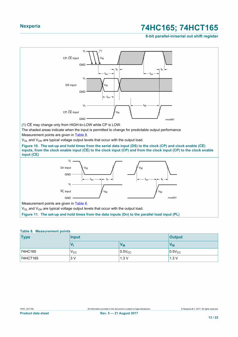
(1) CE may change only from HIGH-to-LOW while CP is LOW.The shaded areas indicate when the input is permitted to change for predictable output performanceMeasurement points are given in Table 8.VOL and VOH are typical voltage output levels that occur with the output load.Figure 10. The set-up and hold times from the serial data input (DS) to the clock (CP) and clock enable (CE)inputs, from the clock enable input (CE) to the clock input (CP) and from the clock input (CP) to the clock enableinput (CE)
mna991
Dn input
PL input
tsu th
VI
GND
VI
GND
VM
VM
tsu th
VM
VM
Measurement points are given in Table 8.VOL and VOH are typical voltage output levels that occur with the output load.Figure 11. The set-up and hold times from the data inputs (Dn) to the parallel load input (PL)
Table 8. Measurement pointsInput OutputType
VI VM VM
74HC165 VCC 0.5VCC 0.5VCC
74HCT165 3 V 1.3 V 1.3 V

Nexperia 74HC165; 74HCT1658-bit parallel-in/serial out shift register
74HC_HCT165 All information provided in this document is subject to legal disclaimers. © Nexperia B.V. 2017. All rights reserved.
Product data sheet Rev. 5 — 21 August 201714 / 22
VM VM
tW
tW
10 %
90 %
0 V
VI
VI
negativepulse
positivepulse
0 V
VM VM
90 %
10 %
tf
tr
tr
tf
001aad983
DUT
VCC VCC
VI VO
RT
RL S1
CL
openG
Test data is given in Table 9.Definitions for test circuit:RT = Termination resistance should be equal to output impedance Zo of the pulse generator.CL = Load capacitance including jig and probe capacitance.RL = Load resistance.S1 = Test selection switch
Figure 12. Test circuit for measuring switching times
Table 9. Test dataInput Load S1 positionType
VI tr, tf CL RL tPHL, tPLH
74HC165 VCC 6 ns 15 pF, 50 pF 1 kΩ open
74HCT165 3 V 6 ns 15 pF, 50 pF 1 kΩ open

Nexperia 74HC165; 74HCT1658-bit parallel-in/serial out shift register
74HC_HCT165 All information provided in this document is subject to legal disclaimers. © Nexperia B.V. 2017. All rights reserved.
Product data sheet Rev. 5 — 21 August 201715 / 22
12 Package outline
X
w M
θ
AA1A2
bp
D
HE
Lp
Q
detail X
E
Z
e
c
L
v M A
(A )3
A
8
9
1
16
y
pin 1 index
UNITA
max. A1 A2 A3 bp c D(1) E (1) (1)e HE L Lp Q Zywv θ
REFERENCESOUTLINEVERSION
EUROPEANPROJECTION ISSUE DATE
IEC JEDEC JEITA
mm
inches
1.75 0.250.10
1.451.25 0.25 0.49
0.360.250.19
10.09.8
4.03.8 1.27 6.2
5.80.70.6
0.70.3 8
0
oo
0.25 0.1
DIMENSIONS (inch dimensions are derived from the original mm dimensions)
Note1. Plastic or metal protrusions of 0.15 mm (0.006 inch) maximum per side are not included.
1.00.4
SOT109-1 99-12-2703-02-19076E07 MS-012
0.069 0.0100.004
0.0570.049 0.01 0.019
0.0140.01000.0075
0.390.38
0.160.15 0.05
1.05
0.0410.2440.228
0.0280.020
0.0280.0120.01
0.25
0.01 0.0040.0390.016
0 2.5 5 mm
scale
SO16: plastic small outline package; 16 leads; body width 3.9 mm SOT109-1
Figure 13. Package outline SOT109-1 (SO16)

Nexperia 74HC165; 74HCT1658-bit parallel-in/serial out shift register
74HC_HCT165 All information provided in this document is subject to legal disclaimers. © Nexperia B.V. 2017. All rights reserved.
Product data sheet Rev. 5 — 21 August 201716 / 22
UNIT A1 A2 A3 bp c D (1) E (1) e HE L Lp Q Zywv θ
REFERENCESOUTLINEVERSION
EUROPEANPROJECTION ISSUE DATE
IEC JEDEC JEITA
mm 0.210.05
1.801.65 0.25 0.38
0.250.200.09
6.46.0
5.45.2 0.65 1.257.9
7.61.030.63
0.90.7
1.000.55
80
oo0.130.2 0.1
DIMENSIONS (mm are the original dimensions)
Note1. Plastic or metal protrusions of 0.25 mm maximum per side are not included.
SOT338-1 99-12-2703-02-19
(1)
w Mbp
D
HE
E
Z
e
c
v M A
XA
y
1 8
16 9
θ
AA1A2
Lp
Q
detail X
L
(A )3
MO-150
pin 1 index
0 2.5 5 mm
scale
SSOP16: plastic shrink small outline package; 16 leads; body width 5.3 mm SOT338-1
Amax.
2
Figure 14. Package outline SOT338-1 (SSOP16)

Nexperia 74HC165; 74HCT1658-bit parallel-in/serial out shift register
74HC_HCT165 All information provided in this document is subject to legal disclaimers. © Nexperia B.V. 2017. All rights reserved.
Product data sheet Rev. 5 — 21 August 201717 / 22
UNIT A1 A2 A3 bp c D (1) E (2) (1)e HE L Lp Q Zywv θ
REFERENCESOUTLINEVERSION
EUROPEANPROJECTION ISSUE DATE
IEC JEDEC JEITA
mm 0.150.05
0.950.80
0.300.19
0.20.1
5.14.9
4.54.3 0.65 6.6
6.20.40.3
0.400.06
80
oo0.13 0.10.21
DIMENSIONS (mm are the original dimensions)
Notes1. Plastic or metal protrusions of 0.15 mm maximum per side are not included.2. Plastic interlead protrusions of 0.25 mm maximum per side are not included.
0.750.50
SOT403-1 MO-153 99-12-2703-02-18
w Mbp
D
Z
e
0.25
1 8
16 9
θ
AA1A2
Lp
Q
detail X
L
(A )3
HE
E
c
v M A
XA
y
0 2.5 5 mm
scale
TSSOP16: plastic thin shrink small outline package; 16 leads; body width 4.4 mm SOT403-1
Amax.
1.1
pin 1 index
Figure 15. Package outline SOT403-1 (TSSOP16)

Nexperia 74HC165; 74HCT1658-bit parallel-in/serial out shift register
74HC_HCT165 All information provided in this document is subject to legal disclaimers. © Nexperia B.V. 2017. All rights reserved.
Product data sheet Rev. 5 — 21 August 201718 / 22
terminal 1index area
0.51
A1 EhbUNIT ye
0.2
c
REFERENCESOUTLINEVERSION
EUROPEANPROJECTION ISSUE DATE
IEC JEDEC JEITA
mm 3.63.4
Dh
2.151.85
y1
2.62.4
1.150.85
e1
2.50.300.18
0.050.00 0.05 0.1
DIMENSIONS (mm are the original dimensions)
SOT763-1 MO-241 - - -- - -
0.50.3
L
0.1
v
0.05
w
0 2.5 5 mm
scale
SOT763-1DHVQFN16: plastic dual in-line compatible thermal enhanced very thin quad flat package; no leads;16 terminals; body 2.5 x 3.5 x 0.85 mm
A(1)
max.
AA1
c
detail X
yy1 Ce
L
Eh
Dh
e
e1
b
2 7
15 10
9
81
16
X
D
E
C
B A
terminal 1index area
ACC
Bv M
w M
E(1)
Note1. Plastic or metal protrusions of 0.075 mm maximum per side are not included.
D(1)
02-10-1703-01-27
Figure 16. Package outline SOT763-1 (DHVQFN16)

Nexperia 74HC165; 74HCT1658-bit parallel-in/serial out shift register
74HC_HCT165 All information provided in this document is subject to legal disclaimers. © Nexperia B.V. 2017. All rights reserved.
Product data sheet Rev. 5 — 21 August 201719 / 22
13 AbbreviationsTable 10. AbbreviationsAcronym DescriptionCMOS Complementary Metal-Oxide Semiconductor
DUT Device Under Test
ESD ElectroStatic Discharge
HBM Human Body Model
MM Machine Model
TTL Transistor-Transistor Logic
14 Revision historyTable 11. Revision historyDocument ID Release date Data sheet status Change notice Supersedes74HC_HCT165 v.5 20170821 Product data sheet - 74HC_HCT165 v.4
Modifications: • Hold time for 74HC165 has been updated. See Paragraph hold time.• The format of this data sheet has been redesigned to comply with the identity guidelines of
Nexperia.• Legal texts have been adapted to the new company name where appropriate.
74HC_HCT165 v.4 20151228 Product data sheet - 74HC_HCT165 v.3
Modifications: • Type numbers 74HC165N and 74HCT165N (SOT38-4) removed.
74HC_HCT165 v.3 20080314 Product data sheet - 74HC_HCT165_CNV v.2
Modifications: • The format of this data sheet has been redesigned to comply with the new identity guidelinesof NXP Semiconductors.
• Legal texts have been adapted to the new company name where appropriate.• Package SOT763-1 (DHVQFN16) added to Section 4 and Section 12.• Family data added, see Section 10
74HC_HCT165_CNV v.2 December 1990 Product specification - -

Nexperia 74HC165; 74HCT1658-bit parallel-in/serial out shift register
74HC_HCT165 All information provided in this document is subject to legal disclaimers. © Nexperia B.V. 2017. All rights reserved.
Product data sheet Rev. 5 — 21 August 201720 / 22
15 Legal information
15.1 Data sheet status
Document status[1][2] Product status[3] Definition
Objective [short] data sheet Development This document contains data from the objective specification for productdevelopment.
Preliminary [short] data sheet Qualification This document contains data from the preliminary specification.
Product [short] data sheet Production This document contains the product specification.
[1] Please consult the most recently issued document before initiating or completing a design.[2] The term 'short data sheet' is explained in section "Definitions".[3] The product status of device(s) described in this document may have changed since this document was published and may differ in case of multiple
devices. The latest product status information is available on the Internet at URL http://www.nexperia.com.
15.2 DefinitionsDraft — The document is a draft version only. The content is still underinternal review and subject to formal approval, which may result inmodifications or additions. Nexperia does not give any representations orwarranties as to the accuracy or completeness of information included hereinand shall have no liability for the consequences of use of such information.
Short data sheet — A short data sheet is an extract from a full data sheetwith the same product type number(s) and title. A short data sheet isintended for quick reference only and should not be relied upon to containdetailed and full information. For detailed and full information see therelevant full data sheet, which is available on request via the local Nexperiasales office. In case of any inconsistency or conflict with the short data sheet,the full data sheet shall prevail.
Product specification — The information and data provided in a Productdata sheet shall define the specification of the product as agreed betweenNexperia and its customer, unless Nexperia and customer have explicitlyagreed otherwise in writing. In no event however, shall an agreement bevalid in which the Nexperia product is deemed to offer functions and qualitiesbeyond those described in the Product data sheet.
15.3 DisclaimersLimited warranty and liability — Information in this document is believedto be accurate and reliable. However, Nexperia does not give anyrepresentations or warranties, expressed or implied, as to the accuracyor completeness of such information and shall have no liability for theconsequences of use of such information. Nexperia takes no responsibilityfor the content in this document if provided by an information source outsideof Nexperia. In no event shall Nexperia be liable for any indirect, incidental,punitive, special or consequential damages (including - without limitation -lost profits, lost savings, business interruption, costs related to the removalor replacement of any products or rework charges) whether or not suchdamages are based on tort (including negligence), warranty, breach ofcontract or any other legal theory. Notwithstanding any damages thatcustomer might incur for any reason whatsoever, Nexperia's aggregate andcumulative liability towards customer for the products described herein shallbe limited in accordance with the Terms and conditions of commercial sale ofNexperia.
Right to make changes — Nexperia reserves the right to make changesto information published in this document, including without limitationspecifications and product descriptions, at any time and without notice. Thisdocument supersedes and replaces all information supplied prior to thepublication hereof.
Suitability for use — Nexperia products are not designed, authorized orwarranted to be suitable for use in life support, life-critical or safety-critical
systems or equipment, nor in applications where failure or malfunctionof an Nexperia product can reasonably be expected to result in personalinjury, death or severe property or environmental damage. Nexperia and itssuppliers accept no liability for inclusion and/or use of Nexperia products insuch equipment or applications and therefore such inclusion and/or use is atthe customer’s own risk.
Applications — Applications that are described herein for any of theseproducts are for illustrative purposes only. Nexperia makes no representationor warranty that such applications will be suitable for the specified usewithout further testing or modification. Customers are responsible for thedesign and operation of their applications and products using Nexperiaproducts, and Nexperia accepts no liability for any assistance withapplications or customer product design. It is customer’s sole responsibilityto determine whether the Nexperia product is suitable and fit for thecustomer’s applications and products planned, as well as for the plannedapplication and use of customer’s third party customer(s). Customers shouldprovide appropriate design and operating safeguards to minimize the risksassociated with their applications and products. Nexperia does not acceptany liability related to any default, damage, costs or problem which is basedon any weakness or default in the customer’s applications or products, orthe application or use by customer’s third party customer(s). Customer isresponsible for doing all necessary testing for the customer’s applicationsand products using Nexperia products in order to avoid a default of theapplications and the products or of the application or use by customer’s thirdparty customer(s). Nexperia does not accept any liability in this respect.
Limiting values — Stress above one or more limiting values (as defined inthe Absolute Maximum Ratings System of IEC 60134) will cause permanentdamage to the device. Limiting values are stress ratings only and (proper)operation of the device at these or any other conditions above thosegiven in the Recommended operating conditions section (if present) or theCharacteristics sections of this document is not warranted. Constant orrepeated exposure to limiting values will permanently and irreversibly affectthe quality and reliability of the device.
Terms and conditions of commercial sale — Nexperia products aresold subject to the general terms and conditions of commercial sale, aspublished at http://www.nexperia.com/profile/terms, unless otherwise agreedin a valid written individual agreement. In case an individual agreement isconcluded only the terms and conditions of the respective agreement shallapply. Nexperia hereby expressly objects to applying the customer’s generalterms and conditions with regard to the purchase of Nexperia products bycustomer.
No offer to sell or license — Nothing in this document may be interpretedor construed as an offer to sell products that is open for acceptance orthe grant, conveyance or implication of any license under any copyrights,patents or other industrial or intellectual property rights.
Export control — This document as well as the item(s) described hereinmay be subject to export control regulations. Export might require a priorauthorization from competent authorities.

Nexperia 74HC165; 74HCT1658-bit parallel-in/serial out shift register
74HC_HCT165 All information provided in this document is subject to legal disclaimers. © Nexperia B.V. 2017. All rights reserved.
Product data sheet Rev. 5 — 21 August 201721 / 22
Non-automotive qualified products — Unless this data sheet expresslystates that this specific Nexperia product is automotive qualified, theproduct is not suitable for automotive use. It is neither qualified nor tested inaccordance with automotive testing or application requirements. Nexperiaaccepts no liability for inclusion and/or use of non-automotive qualifiedproducts in automotive equipment or applications. In the event that customeruses the product for design-in and use in automotive applications toautomotive specifications and standards, customer (a) shall use the productwithout Nexperia's warranty of the product for such automotive applications,use and specifications, and (b) whenever customer uses the product forautomotive applications beyond Nexperia's specifications such use shall besolely at customer’s own risk, and (c) customer fully indemnifies Nexperiafor any liability, damages or failed product claims resulting from customer
design and use of the product for automotive applications beyond Nexperia'sstandard warranty and Nexperia's product specifications.
Translations — A non-English (translated) version of a document is forreference only. The English version shall prevail in case of any discrepancybetween the translated and English versions.
15.4 TrademarksNotice: All referenced brands, product names, service names andtrademarks are the property of their respective owners.

Nexperia 74HC165; 74HCT1658-bit parallel-in/serial out shift register
Please be aware that important notices concerning this document and the product(s)described herein, have been included in section 'Legal information'.
© Nexperia B.V. 2017. All rights reserved.For more information, please visit: http://www.nexperia.comFor sales office addresses, please send an email to: [email protected]
Date of release: 21 August 2017Document identifier: 74HC_HCT165
Contents1 General description ............................................ 12 Features and benefits .........................................13 Applications .........................................................14 Ordering information .......................................... 25 Functional diagram ............................................. 26 Pinning information ............................................ 36.1 Pinning ...............................................................36.2 Pin description ................................................... 47 Functional description ........................................48 Limiting values ....................................................59 Recommended operating conditions ................ 610 Static characteristics .......................................... 611 Dynamic characteristics .....................................811.1 Waveforms and test circuit .............................. 1112 Package outline .................................................1513 Abbreviations .................................................... 1914 Revision history ................................................ 1915 Legal information ..............................................20
Related Documents


![74HC165; 74HCT165 8-bit parallel-in/serial out shift register · 2016-01-12 · 8-bit parallel-in/serial out shift register [1] The input and output voltage ratings may be exceeded](https://static.cupdf.com/doc/110x72/5e921a9249b0587de52357d2/74hc165-74hct165-8-bit-parallel-inserial-out-shift-2016-01-12-8-bit-parallel-inserial.jpg)