Features • 8-bit Microcontroller Compatible with 8051 Products • Enhanced 8051 Architecture – Single Clock Cycle per Byte Fetch – 12 Clock per Machine Cycle Compatibility Mode – Up to 20 MIPS Throughput at 20 MHz Clock Frequency – Fully Static Operation: 0 Hz to 20 MHz – On-chip 2-cycle Hardware Multiplier – 256 x 8 Internal RAM – External Data/Program Memory Interface – Dual Data Pointers – 4-level Interrupt Priority • Nonvolatile Program and Data Memory – 4K/8K Bytes of In-System Programmable (ISP) Flash Program Memory – 256 Bytes of Flash Data Memory – 256-byte User Signature Array – Endurance: 10,000 Write/Erase Cycles – Serial Interface for Program Downloading – 64-byte Fast Page Programming Mode – 3-level Program Memory Lock for Software Security – In-Application Programming of Program Memory • Peripheral Features – Three 16-bit Timer/Counters with Clock Out Modes – Enhanced UART • Automatic Address Recognition • Framing Error Detection • SPI and TWI Emulation Modes – Programmable Watchdog Timer with Software Reset and Prescaler • Special Microcontroller Features – Brown-out Detection and Power-on Reset with Power-off Flag – Selectable Polarity External Reset Pin – Low Power Idle and Power-down Modes – Interrupt Recovery from Power-down Mode – Internal 1.8432 MHz Auxiliary Oscillator • I/O and Packages – Up to 36 Programmable I/O Lines – Green (Pb/Halide-free) Packages • 40-lead PDIP • 44-lead TQFP/PLCC • 44-pad VQFN/MLF – Configurable Port Modes (per 8-bit port) • Quasi-bidirectional (80C51 Style) • Input-only (Tristate) • Push-pull CMOS Output • Open-drain • Operating Conditions – 2.4V to 5.5V V CC Voltage Range – -40° C to 85°C Temperature Range – 0 to 20 MHz @ 2.4V–5.5V – 0 to 25 MHz @ 4.5V–5.5V 8-bit Microcontroller with 4K/8K Bytes In-System Programmable Flash AT89LP51 AT89LP52 3709D–MICRO–12/11

Welcome message from author
This document is posted to help you gain knowledge. Please leave a comment to let me know what you think about it! Share it to your friends and learn new things together.
Transcript
Features• 8-bit Microcontroller Compatible with 8051 Products• Enhanced 8051 Architecture
– Single Clock Cycle per Byte Fetch– 12 Clock per Machine Cycle Compatibility Mode– Up to 20 MIPS Throughput at 20 MHz Clock Frequency– Fully Static Operation: 0 Hz to 20 MHz– On-chip 2-cycle Hardware Multiplier– 256 x 8 Internal RAM– External Data/Program Memory Interface– Dual Data Pointers– 4-level Interrupt Priority
• Nonvolatile Program and Data Memory– 4K/8K Bytes of In-System Programmable (ISP) Flash Program Memory– 256 Bytes of Flash Data Memory– 256-byte User Signature Array– Endurance: 10,000 Write/Erase Cycles– Serial Interface for Program Downloading– 64-byte Fast Page Programming Mode– 3-level Program Memory Lock for Software Security– In-Application Programming of Program Memory
• Peripheral Features– Three 16-bit Timer/Counters with Clock Out Modes– Enhanced UART
• Automatic Address Recognition• Framing Error Detection• SPI and TWI Emulation Modes
– Programmable Watchdog Timer with Software Reset and Prescaler• Special Microcontroller Features
– Brown-out Detection and Power-on Reset with Power-off Flag– Selectable Polarity External Reset Pin– Low Power Idle and Power-down Modes– Interrupt Recovery from Power-down Mode– Internal 1.8432 MHz Auxiliary Oscillator
• I/O and Packages– Up to 36 Programmable I/O Lines– Green (Pb/Halide-free) Packages
• 40-lead PDIP• 44-lead TQFP/PLCC• 44-pad VQFN/MLF
– Configurable Port Modes (per 8-bit port)• Quasi-bidirectional (80C51 Style)• Input-only (Tristate)• Push-pull CMOS Output• Open-drain
• Operating Conditions– 2.4V to 5.5V VCC Voltage Range– -40° C to 85°C Temperature Range– 0 to 20 MHz @ 2.4V–5.5V– 0 to 25 MHz @ 4.5V–5.5V
8-bit Microcontroller with 4K/8K Bytes In-System Programmable Flash
AT89LP51AT89LP52
3709D–MICRO–12/11
23709D–MICRO–12/11
AT89LP51/52
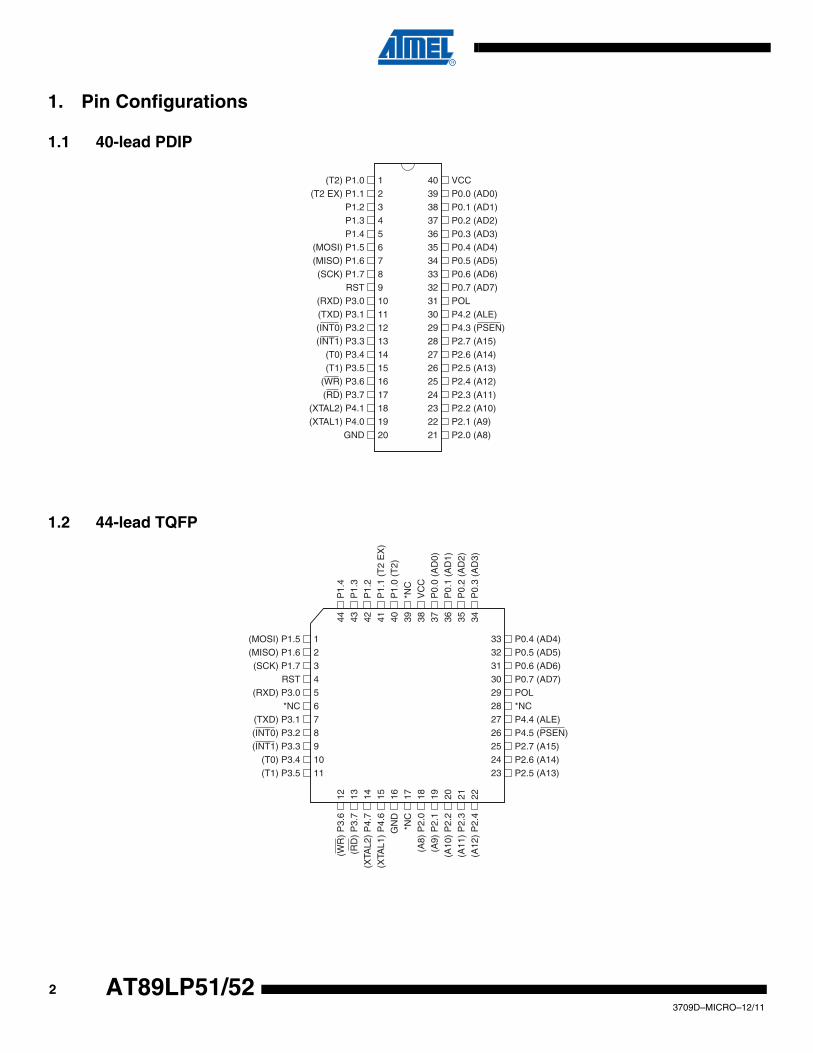
1. Pin Configurations
1.1 40-lead PDIP
1.2 44-lead TQFP
1234567891011121314151617181920
4039383736353433323130292827262524232221
(T2) P1.0(T2 EX) P1.1
P1.2P1.3P1.4
(MOSI) P1.5(MISO) P1.6(SCK) P1.7
RST(RXD) P3.0(TXD) P3.1(INT0) P3.2(INT1) P3.3
(T0) P3.4(T1) P3.5
(WR) P3.6(RD) P3.7
(XTAL2) P4.1(XTAL1) P4.0
GND
VCCP0.0 (AD0)P0.1 (AD1)P0.2 (AD2)P0.3 (AD3)P0.4 (AD4)P0.5 (AD5)P0.6 (AD6)P0.7 (AD7)POLP4.2 (ALE)P4.3 (PSEN)P2.7 (A15)P2.6 (A14)P2.5 (A13)P2.4 (A12)P2.3 (A11)P2.2 (A10)P2.1 (A9)P2.0 (A8)
1 2 3 4 5 6 7 8 9 10 11
33 32 31 30 29 28 27 26 25 24 23
44
43
42
41
40
39
38
37
36
35
34
12
13
14
15
16
17
18
19
20
21
22
(MOSI) P1.5(MISO) P1.6(SCK) P1.7
RST(RXD) P3.0
*NC(TXD) P3.1(INT0) P3.2(INT1) P3.3
(T0) P3.4(T1) P3.5
P0.4 (AD4)P0.5 (AD5)P0.6 (AD6)P0.7 (AD7)POL*NCP4.4 (ALE)P4.5 (PSEN)P2.7 (A15)P2.6 (A14)P2.5 (A13)
P1.
4P
1.3
P1.
2P
1.1
(T2
EX
)P
1.0
(T2)
*NC
VC
CP
0.0
(AD
0)P
0.1
(AD
1)P
0.2
(AD
2)P
0.3
(AD
3)
(WR
) P
3.6
(RD
) P
3.7
(XTA
L2)
P4.
7(X
TAL1
) P
4.6
GN
D*N
C(A
8) P
2.0
(A9)
P2.
1(A
10)
P2.
2(A
11)
P2.
3(A
12)
P2.
4
33709D–MICRO–12/11
AT89LP51/52
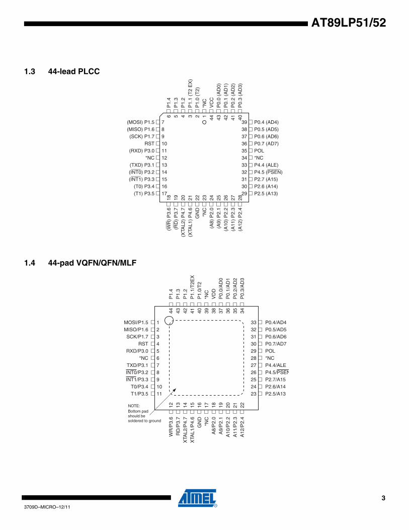
1.3 44-lead PLCC
1.4 44-pad VQFN/QFN/MLF
7 8 9 10 11 12 13 14 15 16 17
39 38 37 36 35 34 33 32 31 30 29
(MOSI) P1.5(MISO) P1.6(SCK) P1.7
RST(RXD) P3.0
*NC(TXD) P3.1(INT0) P3.2(INT1) P3.3
(T0) P3.4(T1) P3.5
P0.4 (AD4)P0.5 (AD5)P0.6 (AD6)P0.7 (AD7)POL*NCP4.4 (ALE)P4.5 (PSEN)P2.7 (A15)P2.6 (A14)P2.5 (A13)
6 5 4 3 2 1 44
43
42
41
40
18
19
20
21
22
23
24
25
26
27
28
(WR
) P
3.6
(RD
) P
3.7
(XTA
L2)
P4.
7(X
TAL1
) P
4.6
GN
D*N
C(A
8) P
2.0
(A9)
P2.
1(A
10)
P2.
2(A
11)
P2.
3(A
12)
P2.
4
P1.
4 P
1.3
P1.
2P
1.1
(T2
EX
)P
1.0
(T2)
*NC
VC
CP
0.0
(AD
0)P
0.1
(AD
1)P
0.2
(AD
2)P
0.3
(AD
3)
1 2 3 4 5 6 7 8 9 10 11
33 32 31 30 29 28 27 26 25 24 23
44
43
42
41
40
39
38
37
36
35
34
12
13
14
15
16
17
18
19
20
21
22
Bottom pad should be soldered to ground
NOTE:
MOSI/P1.5MISO/P1.6SCK/P1.7
RSTRXD/P3.0
*NCTXD/P3.1INT0/P3.2INT1/P3.3
T0/P3.4T1/P3.5
P0.4/AD4P0.5/AD5P0.6/AD6P0.7/AD7POL*NCP4.4/ALEP4.5/PSENP2.7/A15P2.6/A14P2.5/A13
WR
/P3.
6R
D/P
3.7
XTA
L2/P
4.7
XTA
L1/P
4.6
GN
D*N
CA
8/P
2.0
A9/
P2.
1A
10/P
2.2
A11
/P2.
3A
12/P
2.4
P1.
4P
1.3
P1.
2P
1.1/
T2E
XP
1.0/
T2
*NC
VD
DP
0.0/
AD
0P
0.1/
AD
1P
0.2/
AD
2P
0.3/
AD
3
43709D–MICRO–12/11
AT89LP51/52
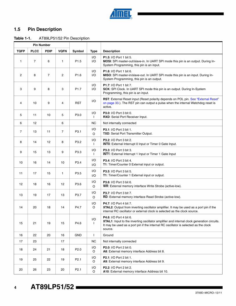
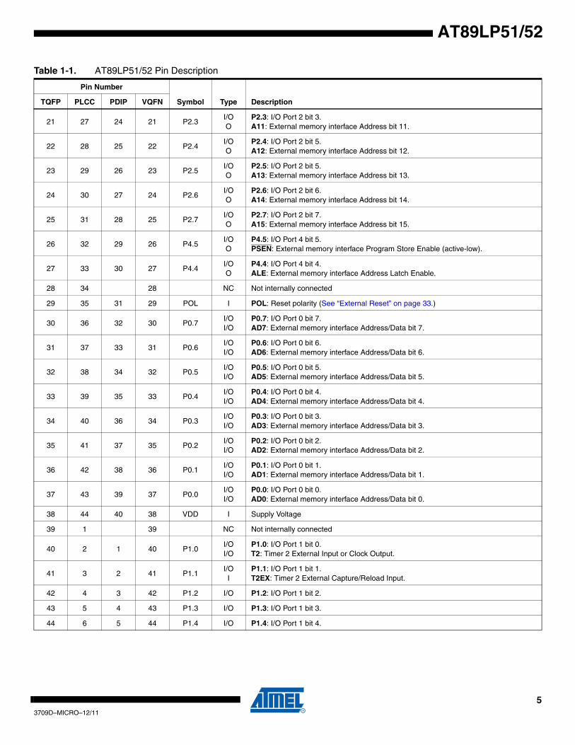
1.5 Pin Description
Table 1-1. AT89LP51/52 Pin Description
Pin Number
Symbol Type DescriptionTQFP PLCC PDIP VQFN
1 7 6 1 P1.5I/OI/O
P1.5: I/O Port 1 bit 5.MOSI: SPI master-out/slave-in. In UART SPI mode this pin is an output. During In-System Programming, this pin is an input.
2 8 7 2 P1.6I/OI/O
P1.6: I/O Port 1 bit 6.MISO: SPI master-in/slave-out. In UART SPI mode this pin is an input. During In-System Programming, this pin is an output.
3 9 8 3 P1.7I/OI/O
P1.7: I/O Port 1 bit 7.SCK: SPI Clock. In UART SPI mode this pin is an output. During In-System Programming, this pin is an input.
4 10 9 4 RSTI/O
RST: External Reset input (Reset polarity depends on POL pin. See “External Reset” on page 33.). The RST pin can output a pulse when the internal Watchdog reset is active.
5 11 10 5 P3.0I/OI
P3.0: I/O Port 3 bit 0.RXD: Serial Port Receiver Input.
6 12 6 NC Not internally connected
7 13 11 7 P3.1I/O
OP3.1: I/O Port 3 bit 1.TXD: Serial Port Transmitter Output.
8 14 12 8 P3.2I/OI
P3.2: I/O Port 3 bit 2.INT0: External Interrupt 0 Input or Timer 0 Gate Input.
9 15 13 9 P3.3I/OI
P3.3: I/O Port 3 bit 3.INT1: External Interrupt 1 Input or Timer 1 Gate Input
10 16 14 10 P3.4I/O
I/OP3.4: I/O Port 3 bit 4.T1: Timer/Counter 0 External input or output.
11 17 15 1 P3.5I/O
I/OP3.5: I/O Port 3 bit 5.T1: Timer/Counter 1 External input or output.
12 18 16 12 P3.6I/O
OP3.6: I/O Port 3 bit 6.WR: External memory interface Write Strobe (active-low).
13 19 17 13 P3.7I/O
OP3.7: I/O Port 3 bit 7.RD: External memory interface Read Strobe (active-low).
14 20 18 14 P4.7I/OO
P4.7: I/O Port 4 bit 7.XTAL2: Output from inverting oscillator amplifier. It may be used as a port pin if the internal RC oscillator or external clock is selected as the clock source.
15 21 19 15 P4.6I/OI
P4.6: I/O Port 4 bit 6.XTAL1: Input to the inverting oscillator amplifier and internal clock generation circuits. It may be used as a port pin if the internal RC oscillator is selected as the clock source.
16 22 20 16 GND I Ground
17 23 17 NC Not internally connected
18 24 21 18 P2.0I/OO
P2.0: I/O Port 2 bit 0.A8: External memory interface Address bit 8.
19 25 22 19 P2.1I/OO
P2.1: I/O Port 2 bit 1.A9: External memory interface Address bit 9.
20 26 23 20 P2.1I/OO
P2.2: I/O Port 2 bit 2.A10: External memory interface Address bit 10.
53709D–MICRO–12/11
AT89LP51/52
21 27 24 21 P2.3I/OO
P2.3: I/O Port 2 bit 3.A11: External memory interface Address bit 11.
22 28 25 22 P2.4I/OO
P2.4: I/O Port 2 bit 5.A12: External memory interface Address bit 12.
23 29 26 23 P2.5I/OO
P2.5: I/O Port 2 bit 5.A13: External memory interface Address bit 13.
24 30 27 24 P2.6I/OO
P2.6: I/O Port 2 bit 6.A14: External memory interface Address bit 14.
25 31 28 25 P2.7I/OO
P2.7: I/O Port 2 bit 7.A15: External memory interface Address bit 15.
26 32 29 26 P4.5I/OO
P4.5: I/O Port 4 bit 5.PSEN: External memory interface Program Store Enable (active-low).
27 33 30 27 P4.4I/OO
P4.4: I/O Port 4 bit 4.ALE: External memory interface Address Latch Enable.
28 34 28 NC Not internally connected
29 35 31 29 POL I POL: Reset polarity (See “External Reset” on page 33.)
30 36 32 30 P0.7I/OI/O
P0.7: I/O Port 0 bit 7.AD7: External memory interface Address/Data bit 7.
31 37 33 31 P0.6I/OI/O
P0.6: I/O Port 0 bit 6.AD6: External memory interface Address/Data bit 6.
32 38 34 32 P0.5I/OI/O
P0.5: I/O Port 0 bit 5.AD5: External memory interface Address/Data bit 5.
33 39 35 33 P0.4I/OI/O
P0.4: I/O Port 0 bit 4.AD4: External memory interface Address/Data bit 4.
34 40 36 34 P0.3I/OI/O
P0.3: I/O Port 0 bit 3.AD3: External memory interface Address/Data bit 3.
35 41 37 35 P0.2I/OI/O
P0.2: I/O Port 0 bit 2.AD2: External memory interface Address/Data bit 2.
36 42 38 36 P0.1I/OI/O
P0.1: I/O Port 0 bit 1.AD1: External memory interface Address/Data bit 1.
37 43 39 37 P0.0I/OI/O
P0.0: I/O Port 0 bit 0.AD0: External memory interface Address/Data bit 0.
38 44 40 38 VDD I Supply Voltage
39 1 39 NC Not internally connected
40 2 1 40 P1.0I/OI/O
P1.0: I/O Port 1 bit 0.T2: Timer 2 External Input or Clock Output.
41 3 2 41 P1.1I/OI
P1.1: I/O Port 1 bit 1.T2EX: Timer 2 External Capture/Reload Input.
42 4 3 42 P1.2 I/O P1.2: I/O Port 1 bit 2.
43 5 4 43 P1.3 I/O P1.3: I/O Port 1 bit 3.
44 6 5 44 P1.4 I/O P1.4: I/O Port 1 bit 4.
Table 1-1. AT89LP51/52 Pin Description
Pin Number
Symbol Type DescriptionTQFP PLCC PDIP VQFN
63709D–MICRO–12/11
AT89LP51/52
2. OverviewThe AT89LP51/52 is a low-power, high-performance CMOS 8-bit microcontroller with 4K/8Kbytes of In-System Programmable Flash program memory and 256 bytes of Flash data memory.The device is manufactured using Atmel's high-density nonvolatile memory technology and iscompatible with the industry-standard 80C52 instruction set.
The AT89LP51/52 is built around an enhanced CPU core that can fetch a single byte from mem-ory every clock cycle. In the classic 8051 architecture, each fetch requires 6 clock cycles, forcinginstructions to execute in 12, 24 or 48 clock cycles. In the AT89LP51/52 CPU, instructions needonly 1 to 4 clock cycles providing 6 to 12 times more throughput than the standard 8051. Sev-enty percent of instructions need only as many clock cycles as they have bytes to execute, andmost of the remaining instructions require only one additional clock. The enhanced CPU core iscapable of 20 MIPS throughput whereas the classic 8051 CPU can deliver only 4 MIPS at thesame current consumption. Conversely, at the same throughput as the classic 8051, the newCPU core runs at a much lower speed and thereby greatly reducing power consumption andEMI. The AT89LP51/52 also includes a compatibility mode that will enable classic 12 clock permachine cycle operation for true timing compatibility with AT89S51/52.
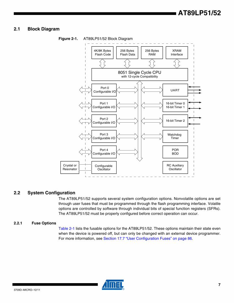
The AT89LP51/52 provides the following standard features: 4K/8K bytes of In-SystemProgrammable Flash program memory, 256 bytes of Flash data memory, 256 bytes of RAM, upto 36 I/O lines, three 16-bit timer/counters, a programmable watchdog timer, a full-duplex serialport, an on-chip crystal oscillator, an internal 1.8432 MHz auxiliary oscillator, and a four-level,six-vector interrupt system. A block diagram is shown in Figure 2-1.
Key Benefits:
• Full software and timing compatibility with AT89S52 means no changes to existing software, including fetching from external ROM or read/write from/to external RAM
• Disable compatibility mode to achieve on average 9 times more throughput at the same current consumption and frequency as AT89S52; or lower the clock frequency 9 times and achieve the same speed as AT89S52 but with more than 5 times less current consumption
• Save even more power and the cost of a quartz crystal by using the internal 1.8432 MHz RC oscillator, which is Vcc and temperature compensated well enough to ensure proper UART serial communications. Together with the built-in POR and the BOD circuits, you do not need any external components for AT89LP52 to provide the reset and clock functions
• All three timer/counters of the AT89LP51/52, Timer 0, Timer 1 and Timer 2, can be configured to toggle a port pin on overflow for clock/waveform generation. Unlike AT89S51, Timer 2 is also present on AT89LP51
• The enhanced full-duplex UART of the AT89LP51/52 includes Framing Error Detection and Automatic Address Recognition. In addition, enhancements to Mode 0 allow hardware accelerated emulation of a master SPI or TWI
• Use In-Application Programming to alter the built-in 8K Flash program memory while executing the application, in effect making it possible to have programmable data tables embedded in the program code. Or use the 256-byte Flash Data memory for nonvolatile data storage
• Each 8-bit I/O port of the AT89LP51/52 can be independently configured in one of four operating modes. In quasi-bidirectional mode, the port operates as in the classic 8051. In input-only mode, the port is tristated. Push-pull output mode provides full CMOS drivers and open-drain mode provides just a pull-down. Unlike other 8051s, this allows Port 0 to operate with on-chip pull-ups if desired
73709D–MICRO–12/11
AT89LP51/52
2.1 Block Diagram
Figure 2-1. AT89LP51/52 Block Diagram
2.2 System ConfigurationThe AT89LP51/52 supports several system configuration options. Nonvolatile options are setthrough user fuses that must be programmed through the flash programming interface. Volatileoptions are controlled by software through individual bits of special function registers (SFRs).The AT89LP51/52 must be properly configured before correct operation can occur.
2.2.1 Fuse OptionsTable 2-1 lists the fusable options for the AT89LP51/52. These options maintain their state evenwhen the device is powered off, but can only be changed with an external device programmer.For more information, see Section 17.7 “User Configuration Fuses” on page 86.
4K/8K Bytes Flash Code
UART
16-bit Timer 016-bit Timer 1
WatchdogTimer
ConfigurableOscillator
Crystal orResonator
256 Bytes Flash Data
16-bit Timer 2
256 BytesRAM
XRAMInterface
8051 Single Cycle CPUwith 12-cycle Compatibility
PORBOD
Port 0Configurable I/O
Port 1Configurable I/O
Port 2Configurable I/O
Port 3Configurable I/O
Port 4Configurable I/O
RC AuxiliaryOscillator
83709D–MICRO–12/11
AT89LP51/52
2.2.2 Software OptionsTable 2-2 lists some important software configuration bits that affect operation at the systemlevel. These can be changed by the application software but are set to their default values uponany reset. Most peripherals also have multipe configuration bits that are not listed here.
2.3 Comparison to AT89S51/52The AT89LP51/52 is part of a family of devices with enhanced features that are fully binary com-patible with the 8051 instruction set. The AT89LP51/52 has two modes of operations,Compatibility mode and Fast mode. In Compatibility mode the instruction timing, peripheralbehavior, SFR addresses, bit assignments and pin functions are identical to Atmel's existingAT89S51/52 product. Additional enhancements are transparent to the user and can be used ifdesired. Fast mode allows greater performance, but with some differences in behavior. Themajor enhancements from the AT89S51/52 are outlined in the following paragraphs and may beuseful to users migrating to the AT89LP51/52 from older devices. A summary of the differencesbetween Compatibility and Fast modes is given in Table 2-3 on page 10. See also the Applica-tion note “Migrating from AT89S52 to AT89LP52.”
Table 2-1. User Configuration Fuses
Fuse Name Description
Clock SourceSelects between the High Speed Crystal Oscillator, Low Speed Crystal Oscillator, External Clock or Internal RC Oscillator for the source of the system clock.
Start-up Time Selects time-out delay for the POR/BOD/PWD wake-up period.
Compatibility ModeConfigures the CPU in 12-clock Compatibility mode or single-cycle Fast mode
In-System Programming Enable Enables or disables In-System Programming.
User Signature Programming Enables or disables programming of User Signature array.
Tristate PortsConfigures the default port state as input-only mode (tristated) or quasi-bidirectional mode (weakly pulled high).
In-Application Programming Enables or disables In-Application (self) Programming
R1 Enable
Table 2-2. Important Software Configuration Bits
Bit(s) SFR Location Description
PxM0PxM1
PMODConfigures the I/O mode of all pins of Port x to be nput-only, quasi-bidirectional, push-pull output or open-drain. The default state is controlled by the Default Port State fuse above
CDV2-0 CLKREG.3-1 Selects the division ratio between the oscillator and the system clock
TPS3-0 CLKREG.7-4 Selects the division ratio between the system clock and the timers
DISALE AUXR.0 Enables/disables toggling of ALE
EXRAM AUXR.1Enables/disables access to on-chip memories that are mapped to the external data memory address space
WS1-0 AUXR.3-2Selects the number of wait states when accessing external data memory
DMEN MEMCON.3 Enables/disables access to the on-chip flash data memory
IAP MEMCON.7 Enbles/disables the self programming feature when the fuse allows
93709D–MICRO–12/11
AT89LP51/52
2.3.1 Instruction ExecutionIn Compatibility mode the AT89LP51/52 CPU uses the six-state machine cycle of the standard8051 where instruction bytes are fetched every three system clock cycles. Execution times inthis mode are identical to AT89S51/52. For greater performance the user can enable Fast modeby disabling the Compatibility fuse. In Fast mode the CPU fetches one code byte from memoryevery clock cycle instead of every three clock cycles. This greatly increases the throughput ofthe CPU. Each standard instruction executes in only 1 to 4 clock cycles. See “Instruction SetSummary” on page 75 for more details. Any software delay loops or instruction-based timingoperations may need to be retuned to achieve the desired results in Fast mode.
2.3.2 System ClockBy default in Compatibility mode the system clock frequency is divided by 2 from the externallysupplied XTAL1 frequency for compatibility with standard 8051s (12 clocks per machine cycle).The System Clock Divider can scale the system clock versus the oscillator source (See Section6.4 on page 31). The divide-by-2 can be disabled to operate in X2 mode (6 clocks per machinecycle) or the clock may be further divided to reduce the operating frequency. In Fast mode theclock divider defaults to divide by 1.
The system clock source is selectable between the crystal oscillator, an externally driven clockand an internal 1.8432 MHz auxiliary oscillator. See “System Clock” on page 29 and “User Con-figuration Fuses” on page 86.
2.3.3 ResetThe RST pin of the AT89LP51/52 has selectable polarity using the POL pin (formerly EA). WhenPOL is high the RST pin is active high with a pull-down resistor and when POL is low the RSTpin is active low with a pull-up resistor. For existing AT89S51/52 sockets where EA is tied toVDD, replacing AT89S51/52 with AT89LP51/52 will maintain the active high reset. Note thatforcing external execution by tying EA low is not supported.
The AT89LP51/52 includes an on-chip Power-On Reset and Brown-out Detector circuit thatensures that the device is reset from system power up. In most cases a RC startup circuit is notrequired on the RST pin, reducing system cost, and the RST pin may be left unconnected if aboard-level reset is not present.
2.3.4 Timer/CountersA common prescaler is available to divide the time base for Timer 0, Timer 1, Timer 2 and theWDT. The TPS3-0 bits in the CLKREG SFR control the prescaler (Table 6-2 on page 31). InCompatibility mode TPS3-0 defaults to 0101B, which causes the timers to count once everymachine cycle. The counting rate can be adjusted linearly from the system clock rate to 1/16 ofthe system clock rate by changing TPS3-0. In Fast mode TPS3-0 defaults to 0000B, or the systemclock rate. TPS does not affect Timer 2 in Clock Out or Baud Generator modes.
In Compatibility mode the sampling of the external Timer/Counter pins: T0, T1, T2 and T2EX;and the external interrupt pins, INT0 and INT1, is also controlled by the prescaler. In Fast modethese pins are always sampled at the system clock rate.
Both Timer 0 and Timer 1 can toggle their respective counter pins, T0 and T1, when they over-flow by setting the output enable bits in TCONB.
The Watchdog Timer includes a 7-bit prescaler for longer timeout periods than the AT89S51/52.Note that in Fast Mode the WDIDLE and DISRTO bits are located in WDTCON and not inAUXR.
103709D–MICRO–12/11
AT89LP51/52
2.3.5 Interrupt HandlingWith the addition of the IPH register, the AT89LP51/52 provides four levels of interrupt priorityfor greater flexibility in handling multiple interrupts. Also, Fast mode allows for faster interruptresponse due to the shorter instruction execution times.
2.3.6 Serial PortThe timer prescaler increases the range of achievable baud rates when using Timer 1 to gener-ate the baud rate in UART Modes 1 or 3, including an increase in the maximum baud rateavailable in Compatibility mode. Additional features include automatic address recognition andframing error detection.
The shift register mode (Mode 0) has been enhanced with more control of the polarity, phaseand frequency of the clock and full-duplex operation. This allows emulation of master serialpheriperal (SPI) and two-wire (TWI) interfaces.
2.3.7 I/O PortsThe P0, P1, P2 and P3 I/O ports of the AT89LP51/52 may be configured in four different modes.The default setting depends on the Tristate-Port User Fuse (See Section 17.7 on page 86).When the fuse is set all the I/O ports revert to input-only (tristated) mode at power-up or reset.When the fuse is not active, ports P1, P2 and P3 start in quasi-bidirectional mode and P0 startsin open-drain mode. P4 always operates in quasi-bidirectional mode. P0 can be configured tohave internal pull-ups by placing it in quasi-bidirectional or output modes. This can reduce sys-tem cost by removing the need for external pull-ups on Port 0.
The P4.4–P4.7 pins are additional I/Os that replace the normally dedicated ALE, PSEN, XTAL1and XTAL2 pins of the AT89S51/52. These pins can be used as additional I/Os depending onthe configuration of the clock and external memory.
2.3.8 SecurityThe AT89LP51/52 does not support the extenal access pin (EA). Therefore it is not possible toexecute from external program memory in address range 0000H–1FFFH. When the third Lockbitis enabled (Lock Mode 4) external program execution is disabled for all addresses above1FFFH. This differs from AT89S51/52 where Lock Mode 4 prevents EA from being sampled low,but may still allow external execution at addresses outside the 8K internal space.
2.3.9 ProgrammingThe AT89LP51/52 supports a richer command set for In-System Programming (ISP). ExistingAT89S51/52 programmers should be able to program the AT89LP51/52 in byte mode. In pagemode the AT89LP51/52 only supports programming of a half-page of 64 bytes and thereforerequires an extra address byte as compared to AT89S51/52. Furthermore the device signatureis located at addresses 0000H, 0001H and 0003H instead of 0000H, 0100H and 0200H.
Table 2-3. Compatibility Mode versus Fast Mode Summary
Feature Compatibility Fast
Instruction Fetch in System Clocks 3 1
Instruction Execution Time in System Clocks 6, 12, 18 or 24 1, 2, 3, 4 or 5
Default System Clock Divisor 2 1
Default Timer Prescaler Divisor 6 1
113709D–MICRO–12/11
AT89LP51/52
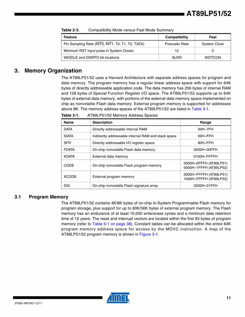
3. Memory OrganizationThe AT89LP51/52 uses a Harvard Architecture with separate address spaces for program anddata memory. The program memory has a regular linear address space with support for 64Kbytes of directly addressable application code. The data memory has 256 bytes of internal RAMand 128 bytes of Special Function Register I/O space. The AT89LP51/52 supports up to 64Kbytes of external data memory, with portions of the external data memory space implemented onchip as nonvolatile Flash data memory. External program memory is supported for addressesabove 8K. The memory address spaces of the AT89LP51/52 are listed in Table 3-1.
3.1 Program MemoryThe AT89LP51/52 contains 4K/8K bytes of on-chip In-System Programmable Flash memory forprogram storage, plus support for up to 60K/56K bytes of external program memory. The Flashmemory has an endurance of at least 10,000 write/erase cycles and a minimum data retentiontime of 10 years. The reset and interrupt vectors are located within the first 83 bytes of programmemory (refer to Table 9-1 on page 38). Constant tables can be allocated within the entire 64Kprogram memory address space for access by the MOVC instruction. A map of theAT89LP51/52 program memory is shown in Figure 3-1.
Pin Sampling Rate (INT0, INT1, T0, T1, T2, T2EX) Prescaler Rate System Clock
Minimum RST input pulse in System Clocks 12 2
WDIDLE and DISRTO bit locations AUXR WDTCON
Table 2-3. Compatibility Mode versus Fast Mode Summary
Feature Compatibility Fast
Table 3-1. AT89LP51/52 Memory Address Spaces
Name Description Range
DATA Directly addressable internal RAM 00H–7FH
IDATA Indirectly addressable internal RAM and stack space 00H–FFH
SFR Directly addressable I/O register space 80H–FFH
FDATA On-chip nonvolatile Flash data memory 0000H–00FFH
XDATA External data memory 0100H–FFFFH
CODE On-chip nonvolatile Flash program memory0000H–0FFFH (AT89LP51)0000H–1FFFH (AT89LP52)
XCODE External program memory2000H–FFFFH (AT89LP51)1000H–FFFFH (AT89LP52)
SIG On-chip nonvolatile Flash signature array 0000H–01FFH
123709D–MICRO–12/11
AT89LP51/52
Figure 3-1. Program Memory Map
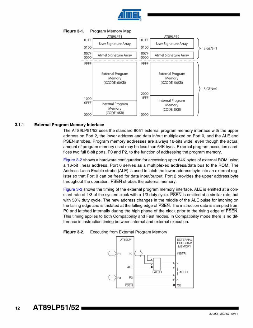
3.1.1 External Program Memory InterfaceThe AT89LP51/52 uses the standard 8051 external program memory interface with the upperaddress on Port 2, the lower address and data in/out multiplexed on Port 0, and the ALE andPSEN strobes. Program memory addresses are always 16-bits wide, even though the actualamount of program memory used may be less than 64K byes. External program execution sacri-fices two full 8-bit ports, P0 and P2, to the function of addressing the program memory.
Figure 3-2 shows a hardware configuration for accessing up to 64K bytes of external ROM usinga 16-bit linear address. Port 0 serves as a multiplexed address/data bus to the ROM. TheAddress Latch Enable strobe (ALE) is used to latch the lower address byte into an external reg-ister so that Port 0 can be freed for data input/output. Port 2 provides the upper address bytethroughout the operation. PSEN strobes the external memory.
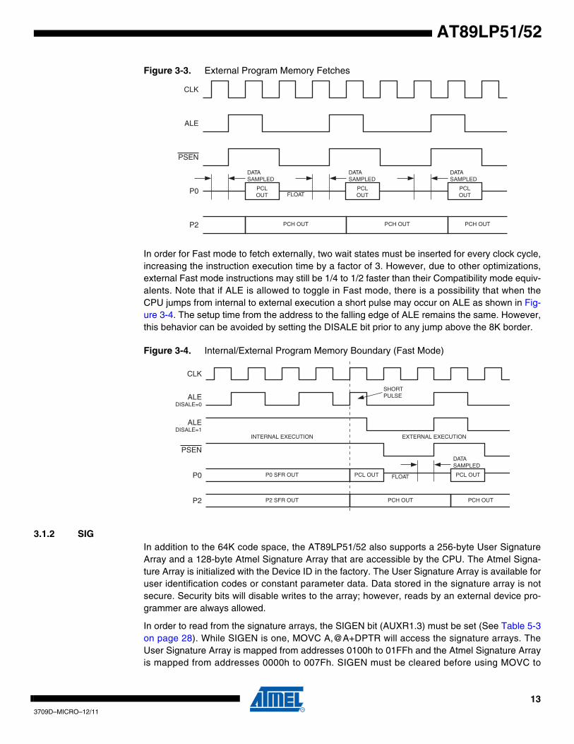
Figure 3-3 shows the timing of the external program memory interface. ALE is emitted at a con-stant rate of 1/3 of the system clock with a 1/3 duty cycle. PSEN is emitted at a similar rate, butwith 50% duty cycle. The new address changes in the middle of the ALE pulse for latching onthe falling edge and is tristated at the falling edge of PSEN. The instruction data is sampled fromP0 and latched internally during the high phase of the clock prior to the rising edge of PSEN.This timing applies to both Compatibility and Fast modes. In Compatibility mode there is no dif-ference in instruction timing between internal and external execution.
Figure 3-2. Executing from External Program Memory
0000
FFFF
0000007F
User Signature Array0100
01FF
Atmel Signature Array
SIGEN=0
SIGEN=1
AT89LP52
20001FFF
External Program Memory
(XCODE: 56KB)
Internal Program Memory
(CODE: 8KB)
0000
FFFF
0000007F
User Signature Array0100
01FF
Atmel Signature Array
AT89LP51
10000FFF
External Program Memory
(XCODE: 60KB)
Internal Program Memory
(CODE: 4KB)
AT89LP EXTERNALPROGRAMMEMORY
INSTR.
ADDR
OEPSEN
P3 P2
ALE
P0P1
LATCH
133709D–MICRO–12/11
AT89LP51/52
Figure 3-3. External Program Memory Fetches
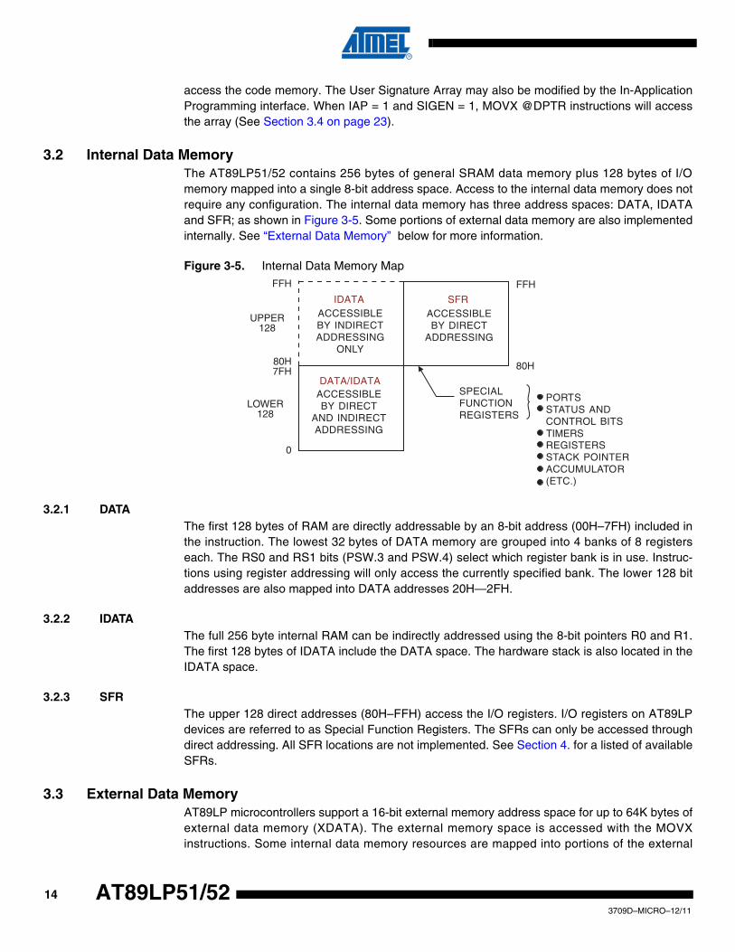
In order for Fast mode to fetch externally, two wait states must be inserted for every clock cycle,increasing the instruction execution time by a factor of 3. However, due to other optimizations,external Fast mode instructions may still be 1/4 to 1/2 faster than their Compatibility mode equiv-alents. Note that if ALE is allowed to toggle in Fast mode, there is a possibility that when theCPU jumps from internal to external execution a short pulse may occur on ALE as shown in Fig-ure 3-4. The setup time from the address to the falling edge of ALE remains the same. However,this behavior can be avoided by setting the DISALE bit prior to any jump above the 8K border.
Figure 3-4. Internal/External Program Memory Boundary (Fast Mode)
3.1.2 SIGIn addition to the 64K code space, the AT89LP51/52 also supports a 256-byte User SignatureArray and a 128-byte Atmel Signature Array that are accessible by the CPU. The Atmel Signa-ture Array is initialized with the Device ID in the factory. The User Signature Array is available foruser identification codes or constant parameter data. Data stored in the signature array is notsecure. Security bits will disable writes to the array; however, reads by an external device pro-grammer are always allowed.
In order to read from the signature arrays, the SIGEN bit (AUXR1.3) must be set (See Table 5-3on page 28). While SIGEN is one, MOVC A,@A+DPTR will access the signature arrays. TheUser Signature Array is mapped from addresses 0100h to 01FFh and the Atmel Signature Arrayis mapped from addresses 0000h to 007Fh. SIGEN must be cleared before using MOVC to
CLK
ALE
PSEN
FLOATPCLOUT
P0
PCH OUTP2 PCH OUT PCH OUT
DATA SAMPLED
PCLOUT
PCLOUT
DATA SAMPLED
DATA SAMPLED
CLK
ALEDISALE=0
PSEN
FLOATP0 SFR OUTP0
P2 SFR OUTP2 PCH OUT PCH OUT
PCL OUT PCL OUT
DATA SAMPLED
SHORTPULSE
ALEDISALE=1
INTERNAL EXECUTION EXTERNAL EXECUTION
143709D–MICRO–12/11
AT89LP51/52
access the code memory. The User Signature Array may also be modified by the In-ApplicationProgramming interface. When IAP = 1 and SIGEN = 1, MOVX @DPTR instructions will accessthe array (See Section 3.4 on page 23).
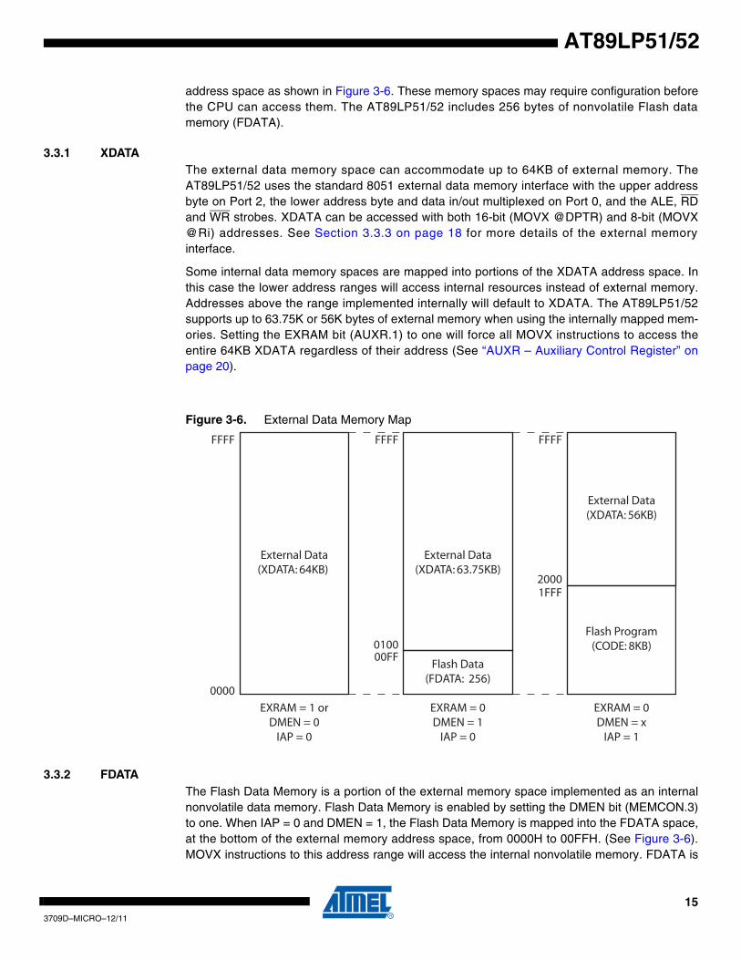
3.2 Internal Data MemoryThe AT89LP51/52 contains 256 bytes of general SRAM data memory plus 128 bytes of I/Omemory mapped into a single 8-bit address space. Access to the internal data memory does notrequire any configuration. The internal data memory has three address spaces: DATA, IDATAand SFR; as shown in Figure 3-5. Some portions of external data memory are also implementedinternally. See “External Data Memory” below for more information.
Figure 3-5. Internal Data Memory Map
3.2.1 DATAThe first 128 bytes of RAM are directly addressable by an 8-bit address (00H–7FH) included inthe instruction. The lowest 32 bytes of DATA memory are grouped into 4 banks of 8 registerseach. The RS0 and RS1 bits (PSW.3 and PSW.4) select which register bank is in use. Instruc-tions using register addressing will only access the currently specified bank. The lower 128 bitaddresses are also mapped into DATA addresses 20H—2FH.
3.2.2 IDATAThe full 256 byte internal RAM can be indirectly addressed using the 8-bit pointers R0 and R1.The first 128 bytes of IDATA include the DATA space. The hardware stack is also located in theIDATA space.
3.2.3 SFRThe upper 128 direct addresses (80H–FFH) access the I/O registers. I/O registers on AT89LPdevices are referred to as Special Function Registers. The SFRs can only be accessed throughdirect addressing. All SFR locations are not implemented. See Section 4. for a listed of availableSFRs.
3.3 External Data MemoryAT89LP microcontrollers support a 16-bit external memory address space for up to 64K bytes ofexternal data memory (XDATA). The external memory space is accessed with the MOVXinstructions. Some internal data memory resources are mapped into portions of the external
FFH
UPPER128
80H7FH
LOWER128
0
ACCESSIBLEBY DIRECT
ADDRESSING
FFH
80H
ACCESSIBLEBY DIRECT
AND INDIRECTADDRESSING
SPECIALFUNCTIONREGISTERS
PORTSSTATUS ANDCONTROL BITS
REGISTERSSTACK POINTERACCUMULATOR(ETC.)
TIMERS
ACCESSIBLEBY INDIRECTADDRESSING
ONLY
IDATA SFR
DATA/IDATA
153709D–MICRO–12/11
AT89LP51/52
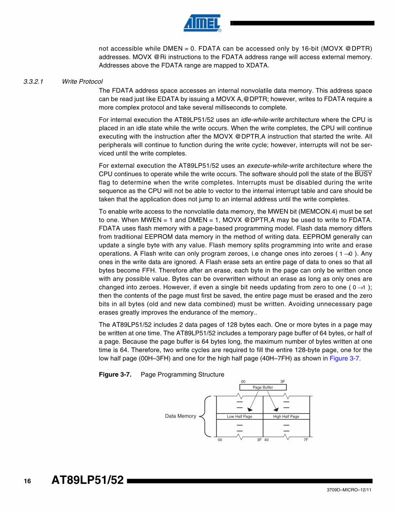
address space as shown in Figure 3-6. These memory spaces may require configuration beforethe CPU can access them. The AT89LP51/52 includes 256 bytes of nonvolatile Flash datamemory (FDATA).
3.3.1 XDATAThe external data memory space can accommodate up to 64KB of external memory. TheAT89LP51/52 uses the standard 8051 external data memory interface with the upper addressbyte on Port 2, the lower address byte and data in/out multiplexed on Port 0, and the ALE, RDand WR strobes. XDATA can be accessed with both 16-bit (MOVX @DPTR) and 8-bit (MOVX@Ri) addresses. See Section 3.3.3 on page 18 for more details of the external memoryinterface.
Some internal data memory spaces are mapped into portions of the XDATA address space. Inthis case the lower address ranges will access internal resources instead of external memory.Addresses above the range implemented internally will default to XDATA. The AT89LP51/52supports up to 63.75K or 56K bytes of external memory when using the internally mapped mem-ories. Setting the EXRAM bit (AUXR.1) to one will force all MOVX instructions to access theentire 64KB XDATA regardless of their address (See “AUXR – Auxiliary Control Register” onpage 20).
Figure 3-6. External Data Memory Map
3.3.2 FDATAThe Flash Data Memory is a portion of the external memory space implemented as an internalnonvolatile data memory. Flash Data Memory is enabled by setting the DMEN bit (MEMCON.3)to one. When IAP = 0 and DMEN = 1, the Flash Data Memory is mapped into the FDATA space,at the bottom of the external memory address space, from 0000H to 00FFH. (See Figure 3-6).MOVX instructions to this address range will access the internal nonvolatile memory. FDATA is
Flash Data(FDATA: 256)
00FF
1FFF2000
Flash Program(CODE: 8KB)
0000
0100
FFFF
External Data (XDATA: 64KB)
External Data(XDATA: 63.75KB)
External Data(XDATA: 56KB)
FFFF FFFF
EXRAM = 1 orDMEN = 0
IAP = 0
EXRAM = 0DMEN = 1
IAP = 0
EXRAM = 0DMEN = x
IAP = 1
163709D–MICRO–12/11
AT89LP51/52
not accessible while DMEN = 0. FDATA can be accessed only by 16-bit (MOVX @DPTR)addresses. MOVX @Ri instructions to the FDATA address range will access external memory.Addresses above the FDATA range are mapped to XDATA.
3.3.2.1 Write ProtocolThe FDATA address space accesses an internal nonvolatile data memory. This address spacecan be read just like EDATA by issuing a MOVX A,@DPTR; however, writes to FDATA require amore complex protocol and take several milliseconds to complete.
For internal execution the AT89LP51/52 uses an idle-while-write architecture where the CPU isplaced in an idle state while the write occurs. When the write completes, the CPU will continueexecuting with the instruction after the MOVX @DPTR,A instruction that started the write. Allperipherals will continue to function during the write cycle; however, interrupts will not be ser-viced until the write completes.
For external execution the AT89LP51/52 uses an execute-while-write architecture where theCPU continues to operate while the write occurs. The software should poll the state of the BUSYflag to determine when the write completes. Interrupts must be disabled during the writesequence as the CPU will not be able to vector to the internal interrupt table and care should betaken that the application does not jump to an internal address until the write completes.
To enable write access to the nonvolatile data memory, the MWEN bit (MEMCON.4) must be setto one. When MWEN = 1 and DMEN = 1, MOVX @DPTR,A may be used to write to FDATA.FDATA uses flash memory with a page-based programming model. Flash data memory differsfrom traditional EEPROM data memory in the method of writing data. EEPROM generally canupdate a single byte with any value. Flash memory splits programming into write and eraseoperations. A Flash write can only program zeroes, i.e change ones into zeroes ( ). Anyones in the write data are ignored. A Flash erase sets an entire page of data to ones so that allbytes become FFH. Therefore after an erase, each byte in the page can only be written oncewith any possible value. Bytes can be overwritten without an erase as long as only ones arechanged into zeroes. However, if even a single bit needs updating from zero to one ( );then the contents of the page must first be saved, the entire page must be erased and the zerobits in all bytes (old and new data combined) must be written. Avoiding unnecessary pageerases greatly improves the endurance of the memory..
The AT89LP51/52 includes 2 data pages of 128 bytes each. One or more bytes in a page maybe written at one time. The AT89LP51/52 includes a temporary page buffer of 64 bytes, or half ofa page. Because the page buffer is 64 bytes long, the maximum number of bytes written at onetime is 64. Therefore, two write cycles are required to fill the entire 128-byte page, one for thelow half page (00H–3FH) and one for the high half page (40H–7FH) as shown in Figure 3-7.
Figure 3-7. Page Programming Structure
1 0→
0 1→
Low Half Page
00 3F
Data Memory High Half Page
40 7F
00 3F
Page Buffer
173709D–MICRO–12/11
AT89LP51/52
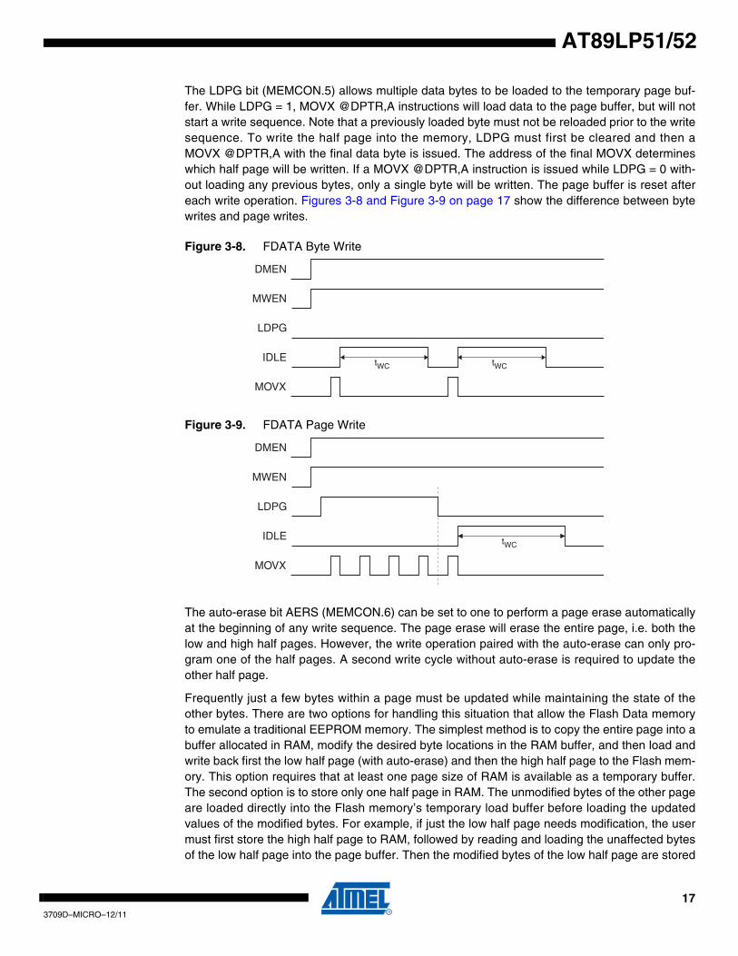
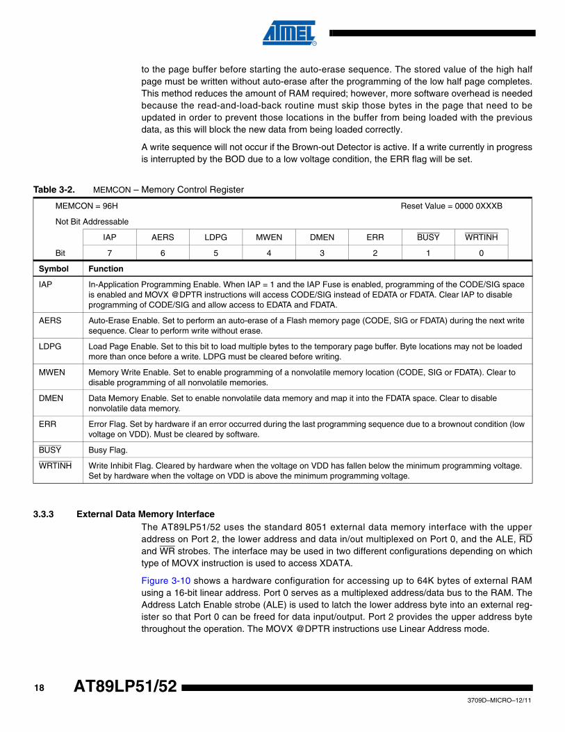
The LDPG bit (MEMCON.5) allows multiple data bytes to be loaded to the temporary page buf-fer. While LDPG = 1, MOVX @DPTR,A instructions will load data to the page buffer, but will notstart a write sequence. Note that a previously loaded byte must not be reloaded prior to the writesequence. To write the half page into the memory, LDPG must first be cleared and then aMOVX @DPTR,A with the final data byte is issued. The address of the final MOVX determineswhich half page will be written. If a MOVX @DPTR,A instruction is issued while LDPG = 0 with-out loading any previous bytes, only a single byte will be written. The page buffer is reset aftereach write operation. Figures 3-8 and Figure 3-9 on page 17 show the difference between bytewrites and page writes.
Figure 3-8. FDATA Byte Write
Figure 3-9. FDATA Page Write
The auto-erase bit AERS (MEMCON.6) can be set to one to perform a page erase automaticallyat the beginning of any write sequence. The page erase will erase the entire page, i.e. both thelow and high half pages. However, the write operation paired with the auto-erase can only pro-gram one of the half pages. A second write cycle without auto-erase is required to update theother half page.
Frequently just a few bytes within a page must be updated while maintaining the state of theother bytes. There are two options for handling this situation that allow the Flash Data memoryto emulate a traditional EEPROM memory. The simplest method is to copy the entire page into abuffer allocated in RAM, modify the desired byte locations in the RAM buffer, and then load andwrite back first the low half page (with auto-erase) and then the high half page to the Flash mem-ory. This option requires that at least one page size of RAM is available as a temporary buffer.The second option is to store only one half page in RAM. The unmodified bytes of the other pageare loaded directly into the Flash memory’s temporary load buffer before loading the updatedvalues of the modified bytes. For example, if just the low half page needs modification, the usermust first store the high half page to RAM, followed by reading and loading the unaffected bytesof the low half page into the page buffer. Then the modified bytes of the low half page are stored
MWEN
DMEN
tWC
LDPG
IDLE
MOVX
tWC
MWEN
DMEN
tWC
LDPG
IDLE
MOVX
183709D–MICRO–12/11
AT89LP51/52
to the page buffer before starting the auto-erase sequence. The stored value of the high halfpage must be written without auto-erase after the programming of the low half page completes.This method reduces the amount of RAM required; however, more software overhead is neededbecause the read-and-load-back routine must skip those bytes in the page that need to beupdated in order to prevent those locations in the buffer from being loaded with the previousdata, as this will block the new data from being loaded correctly.
A write sequence will not occur if the Brown-out Detector is active. If a write currently in progressis interrupted by the BOD due to a low voltage condition, the ERR flag will be set.
3.3.3 External Data Memory InterfaceThe AT89LP51/52 uses the standard 8051 external data memory interface with the upperaddress on Port 2, the lower address and data in/out multiplexed on Port 0, and the ALE, RDand WR strobes. The interface may be used in two different configurations depending on whichtype of MOVX instruction is used to access XDATA.
Figure 3-10 shows a hardware configuration for accessing up to 64K bytes of external RAMusing a 16-bit linear address. Port 0 serves as a multiplexed address/data bus to the RAM. TheAddress Latch Enable strobe (ALE) is used to latch the lower address byte into an external reg-ister so that Port 0 can be freed for data input/output. Port 2 provides the upper address bytethroughout the operation. The MOVX @DPTR instructions use Linear Address mode.
Table 3-2. MEMCON – Memory Control Register
MEMCON = 96H Reset Value = 0000 0XXXB
Not Bit Addressable
IAP AERS LDPG MWEN DMEN ERR BUSY WRTINH
Bit 7 6 5 4 3 2 1 0
Symbol Function
IAP In-Application Programming Enable. When IAP = 1 and the IAP Fuse is enabled, programming of the CODE/SIG space is enabled and MOVX @DPTR instructions will access CODE/SIG instead of EDATA or FDATA. Clear IAP to disable programming of CODE/SIG and allow access to EDATA and FDATA.
AERS Auto-Erase Enable. Set to perform an auto-erase of a Flash memory page (CODE, SIG or FDATA) during the next write sequence. Clear to perform write without erase.
LDPG Load Page Enable. Set to this bit to load multiple bytes to the temporary page buffer. Byte locations may not be loaded more than once before a write. LDPG must be cleared before writing.
MWEN Memory Write Enable. Set to enable programming of a nonvolatile memory location (CODE, SIG or FDATA). Clear to disable programming of all nonvolatile memories.
DMEN Data Memory Enable. Set to enable nonvolatile data memory and map it into the FDATA space. Clear to disable nonvolatile data memory.
ERR Error Flag. Set by hardware if an error occurred during the last programming sequence due to a brownout condition (low voltage on VDD). Must be cleared by software.
BUSY Busy Flag.
WRTINH Write Inhibit Flag. Cleared by hardware when the voltage on VDD has fallen below the minimum programming voltage. Set by hardware when the voltage on VDD is above the minimum programming voltage.
193709D–MICRO–12/11
AT89LP51/52
Figure 3-10. External Data Memory 16-bit Linear Address Mode
Figure 3-11 shows a hardware configuration for accessing 256-byte blocks of external RAMusing an 8-bit paged address. Port 0 serves as a multiplexed address/data bus to the RAM. TheALE strobe is used to latch the address byte into an external register so that Port 0 can be freedfor data input/output. The Port 2 I/O lines (or other ports) can provide control lines to page thememory; however, this operation is not handled automatically by hardware. The software appli-cation must change the Port 2 register when appropriate to access different pages. TheMOVX @Ri instructions use Paged Address mode.
Figure 3-11. External Data Memory 8-bit Paged Address Mode
Note that prior to using the external memory interface, WR (P3.6) and RD (P3.7) must be config-ured as outputs. See Section 10.1 “Port Configuration” on page 41. P0 and P2 are configuredautomatically to push-pull output mode when outputting address or data and P0 is automaticallytristated when inputting data regardless of the port configuration. The Port 0 configuration willdetermine the idle state of Port 0 when not accessing the external memory.
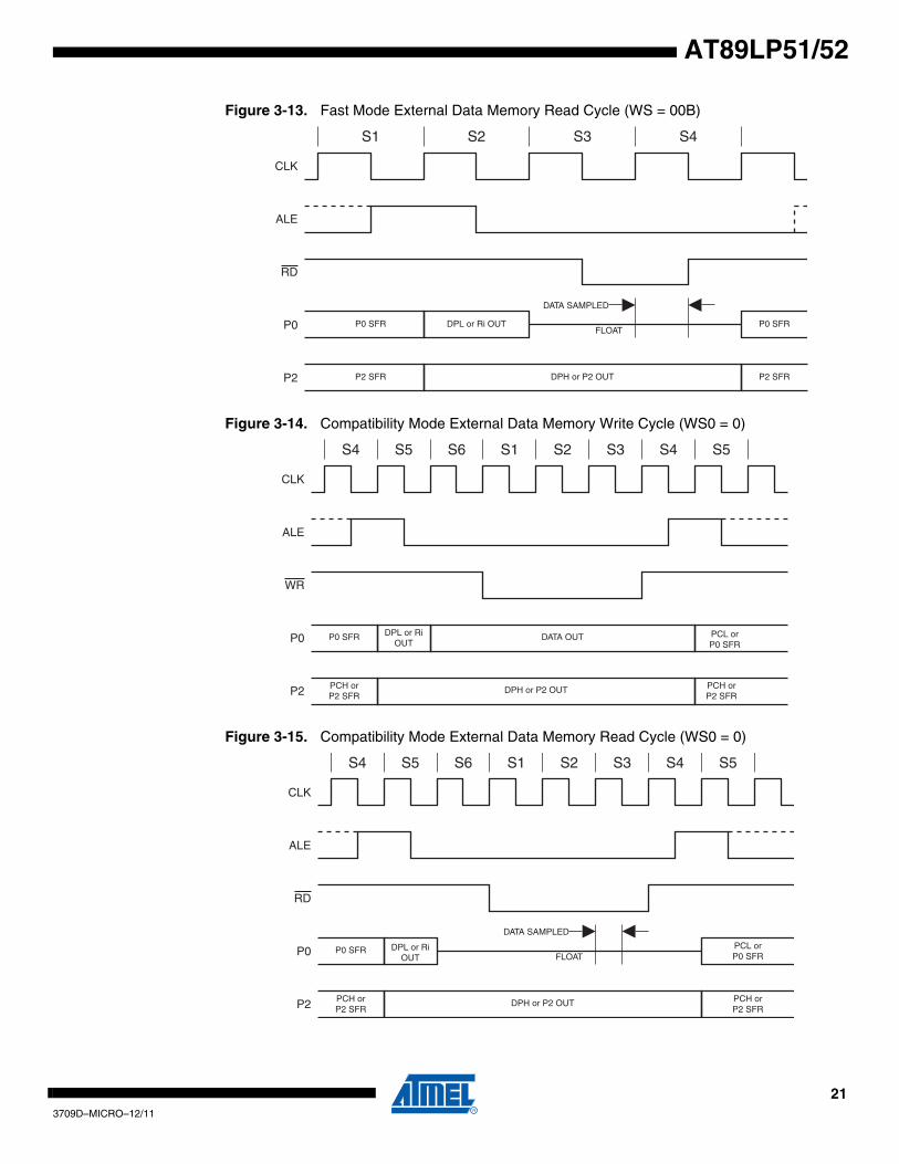
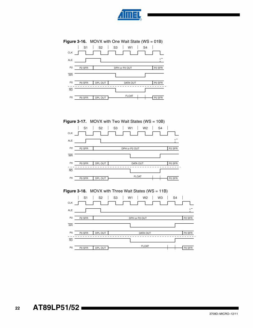
Figure 3-12 and Figure 3-13 show examples of external data memory write and read cycles,respectively. The address on P0 and P2 is stable at the falling edge of ALE. The idle state ofALE is controlled by DISALE (AUXR.0). When DISALE = 0 the ALE toggles at a constant ratewhen not accessing external memory. When DISALE = 1 the ALE is weakly pulled high. DISALEmust be one in order to use P4.4 as a general-purpose I/O. The WS bits in AUXR can extendedthe RD and WR strobes by 1, 2 or 3 cycles as shown in Figures 3-16, 3-17 and 3-18. If a longerstrobe is required, the application can scale the system clock with the clock divider to meet therequirements (See Section 6.4 on page 31).
P1 P0
ALE
P2
RDP3
WR
AT89LP
DATA
LATCH
EXTERNALDATA
MEMORY
WE
ADDR
OE
P1 P0
I/O
ALE
P2RD
P3
WR
AT89LP
DATA
LATCH
EXTERNALDATA
MEMORY
WE
ADDR
PAGEBITS OE
203709D–MICRO–12/11
AT89LP51/52
Notes: 1. AUXR.4 and AUXR.3 function as WDIDLE and DISRTO only in Compatibility mode. In Fast mode these bits are located in WDTCON.
2. WS1 is only available in Fast mode. WS1 is forced to 0 in Compatibility mode.
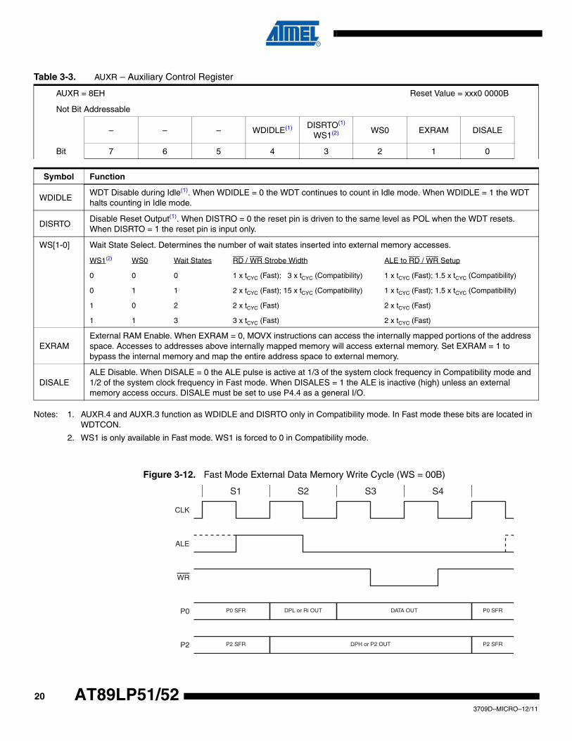
Figure 3-12. Fast Mode External Data Memory Write Cycle (WS = 00B)
Table 3-3. AUXR – Auxiliary Control Register
AUXR = 8EH Reset Value = xxx0 0000B
Not Bit Addressable
– – – WDIDLE(1) DISRTO(1)
WS1(2) WS0 EXRAM DISALE
Bit 7 6 5 4 3 2 1 0
Symbol Function
WDIDLEWDT Disable during Idle(1). When WDIDLE = 0 the WDT continues to count in Idle mode. When WDIDLE = 1 the WDT halts counting in Idle mode.
DISRTODisable Reset Output(1). When DISTRO = 0 the reset pin is driven to the same level as POL when the WDT resets. When DISRTO = 1 the reset pin is input only.
WS[1-0] Wait State Select. Determines the number of wait states inserted into external memory accesses.
WS1(2) WS0 Wait States RD / WR Strobe Width ALE to RD / WR Setup
0 0 0 1 x tCYC (Fast); 3 x tCYC (Compatibility) 1 x tCYC (Fast); 1.5 x tCYC (Compatibility)
0 1 1 2 x tCYC (Fast); 15 x tCYC (Compatibility) 1 x tCYC (Fast); 1.5 x tCYC (Compatibility)
1 0 2 2 x tCYC (Fast) 2 x tCYC (Fast)
1 1 3 3 x tCYC (Fast) 2 x tCYC (Fast)
EXRAMExternal RAM Enable. When EXRAM = 0, MOVX instructions can access the internally mapped portions of the address space. Accesses to addresses above internally mapped memory will access external memory. Set EXRAM = 1 to bypass the internal memory and map the entire address space to external memory.
DISALEALE Disable. When DISALE = 0 the ALE pulse is active at 1/3 of the system clock frequency in Compatibility mode and 1/2 of the system clock frequency in Fast mode. When DISALES = 1 the ALE is inactive (high) unless an external memory access occurs. DISALE must be set to use P4.4 as a general I/O.
S1 S2 S3 S4
CLK
ALE
WR
DPL or Ri OUTP0 SFR P0 SFRP0
P2 SFR P2 SFRDPH or P2 OUTP2
DATA OUT
213709D–MICRO–12/11
AT89LP51/52
Figure 3-13. Fast Mode External Data Memory Read Cycle (WS = 00B)
Figure 3-14. Compatibility Mode External Data Memory Write Cycle (WS0 = 0)
Figure 3-15. Compatibility Mode External Data Memory Read Cycle (WS0 = 0)
S1 S2 S3 S4
CLK
ALE
RD
FLOAT
DATA SAMPLED
DPL or Ri OUTP0 SFR P0 SFRP0
P2 SFR P2 SFRDPH or P2 OUTP2
S4 S5 S6 S1
CLK
ALE
WR
DPL or Ri OUT
P0 SFR PCL orP0 SFR
P0
PCH orP2 SFR
PCH orP2 SFR
DPH or P2 OUTP2
DATA OUT
S2 S3 S4 S5
CLK
ALE
RD
FLOAT
DATA SAMPLED
DPL or Ri OUT
P0 SFR PCL orP0 SFRP0
PCH orP2 SFR
PCH orP2 SFR
DPH or P2 OUTP2
S4 S5 S6 S1 S2 S3 S4 S5
223709D–MICRO–12/11
AT89LP51/52
Figure 3-16. MOVX with One Wait State (WS = 01B)
Figure 3-17. MOVX with Two Wait States (WS = 10B)
Figure 3-18. MOVX with Three Wait States (WS = 11B)
S1 S2 S3 W1
CLK
ALE
WR
DPL OUTP0 SFR P0 SFRP0
P2 SFR P2 SFRDPH or P2 OUTP2
DATA OUT
S4
RD
DPL OUTP0 SFR P0 SFRP0FLOAT
S1 S2 S3 W1
CLK
ALE
WR
DPL OUT P0 SFR P0 SFR P0
P2 SFR P2 SFR DPH or P2 OUT P2
DATA OUT
W2
RD
DPL OUT P0 SFR P0 SFR P0 FLOAT
S4
S1 S2 S3 W1
CLK
ALE
WR
DPL OUT P0 SFR P0 SFR P0
P2 SFR P2 SFR DPH or P2 OUT P2
DATA OUT
W2
RD
DPL OUT P0 SFR P0 SFR P0 FLOAT
W3 S4
233709D–MICRO–12/11
AT89LP51/52
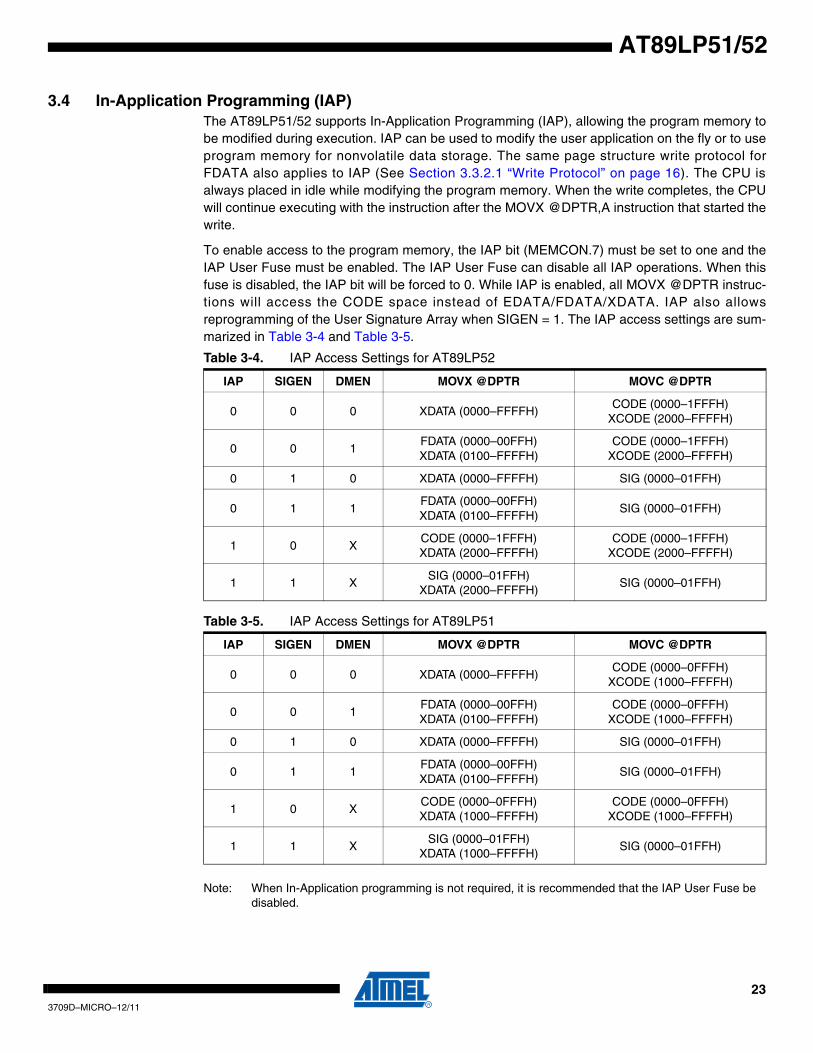
3.4 In-Application Programming (IAP)The AT89LP51/52 supports In-Application Programming (IAP), allowing the program memory tobe modified during execution. IAP can be used to modify the user application on the fly or to useprogram memory for nonvolatile data storage. The same page structure write protocol forFDATA also applies to IAP (See Section 3.3.2.1 “Write Protocol” on page 16). The CPU isalways placed in idle while modifying the program memory. When the write completes, the CPUwill continue executing with the instruction after the MOVX @DPTR,A instruction that started thewrite.
To enable access to the program memory, the IAP bit (MEMCON.7) must be set to one and theIAP User Fuse must be enabled. The IAP User Fuse can disable all IAP operations. When thisfuse is disabled, the IAP bit will be forced to 0. While IAP is enabled, all MOVX @DPTR instruc-tions will access the CODE space instead of EDATA/FDATA/XDATA. IAP also allowsreprogramming of the User Signature Array when SIGEN = 1. The IAP access settings are sum-marized in Table 3-4 and Table 3-5.
Note: When In-Application programming is not required, it is recommended that the IAP User Fuse be disabled.
Table 3-4. IAP Access Settings for AT89LP52
IAP SIGEN DMEN MOVX @DPTR MOVC @DPTR
0 0 0 XDATA (0000–FFFFH)CODE (0000–1FFFH)
XCODE (2000–FFFFH)
0 0 1FDATA (0000–00FFH)XDATA (0100–FFFFH)
CODE (0000–1FFFH)XCODE (2000–FFFFH)
0 1 0 XDATA (0000–FFFFH) SIG (0000–01FFH)
0 1 1FDATA (0000–00FFH)XDATA (0100–FFFFH)
SIG (0000–01FFH)
1 0 XCODE (0000–1FFFH)XDATA (2000–FFFFH)
CODE (0000–1FFFH)XCODE (2000–FFFFH)
1 1 XSIG (0000–01FFH)
XDATA (2000–FFFFH)SIG (0000–01FFH)
Table 3-5. IAP Access Settings for AT89LP51
IAP SIGEN DMEN MOVX @DPTR MOVC @DPTR
0 0 0 XDATA (0000–FFFFH)CODE (0000–0FFFH)
XCODE (1000–FFFFH)
0 0 1FDATA (0000–00FFH)XDATA (0100–FFFFH)
CODE (0000–0FFFH)XCODE (1000–FFFFH)
0 1 0 XDATA (0000–FFFFH) SIG (0000–01FFH)
0 1 1FDATA (0000–00FFH)XDATA (0100–FFFFH)
SIG (0000–01FFH)
1 0 XCODE (0000–0FFFH)XDATA (1000–FFFFH)
CODE (0000–0FFFH)XCODE (1000–FFFFH)
1 1 XSIG (0000–01FFH)
XDATA (1000–FFFFH)SIG (0000–01FFH)
243709D–MICRO–12/11
AT89LP51/52
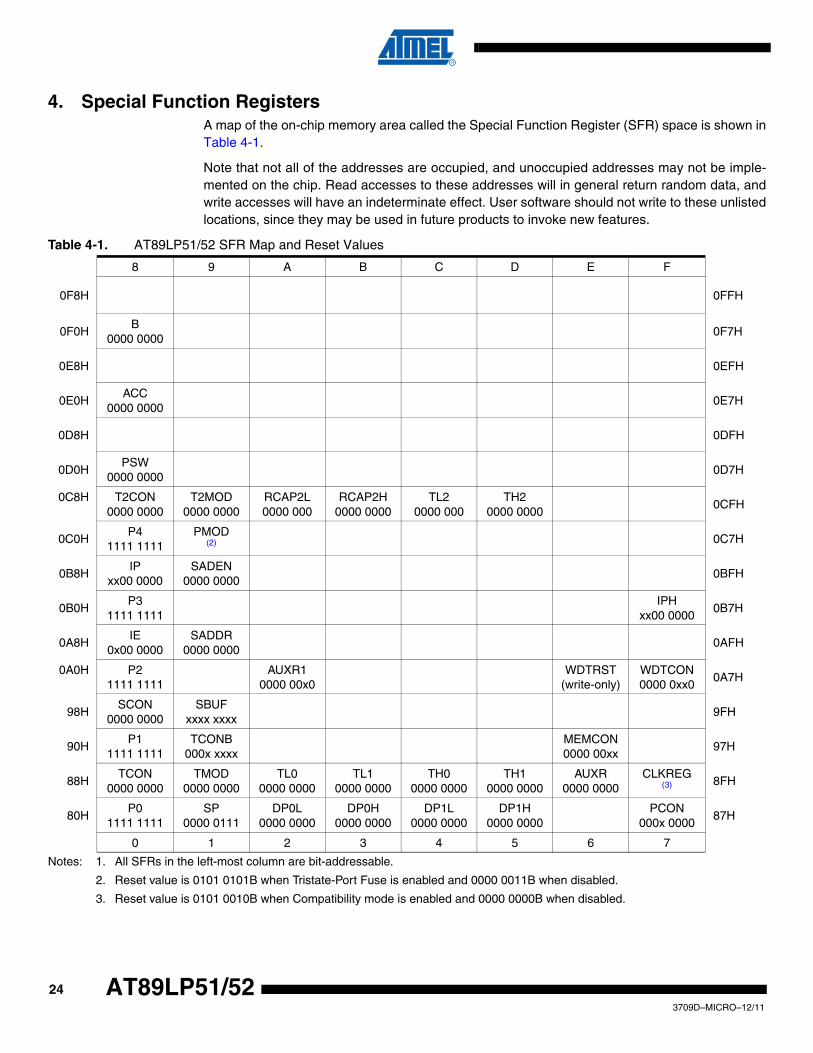
4. Special Function RegistersA map of the on-chip memory area called the Special Function Register (SFR) space is shown inTable 4-1.
Note that not all of the addresses are occupied, and unoccupied addresses may not be imple-mented on the chip. Read accesses to these addresses will in general return random data, andwrite accesses will have an indeterminate effect. User software should not write to these unlistedlocations, since they may be used in future products to invoke new features.
Notes: 1. All SFRs in the left-most column are bit-addressable.
2. Reset value is 0101 0101B when Tristate-Port Fuse is enabled and 0000 0011B when disabled.
3. Reset value is 0101 0010B when Compatibility mode is enabled and 0000 0000B when disabled.
Table 4-1. AT89LP51/52 SFR Map and Reset Values
8 9 A B C D E F
0F8H 0FFH
0F0HB
0000 00000F7H
0E8H 0EFH
0E0HACC
0000 00000E7H
0D8H 0DFH
0D0HPSW
0000 00000D7H
0C8H T2CON0000 0000
T2MOD0000 0000
RCAP2L0000 000
RCAP2H0000 0000
TL20000 000
TH20000 0000
0CFH
0C0HP4
1111 1111PMOD
(2) 0C7H
0B8HIP
xx00 0000SADEN
0000 00000BFH
0B0HP3
1111 1111IPH
xx00 00000B7H
0A8HIE
0x00 0000SADDR
0000 00000AFH
0A0H P21111 1111
AUXR10000 00x0
WDTRST(write-only)
WDTCON0000 0xx0
0A7H
98HSCON
0000 0000SBUF
xxxx xxxx9FH
90HP1
1111 1111TCONB
000x xxxxMEMCON0000 00xx
97H
88HTCON
0000 0000TMOD
0000 0000TL0
0000 0000TL1
0000 0000TH0
0000 0000TH1
0000 0000AUXR
0000 0000CLKREG
(3) 8FH
80HP0
1111 1111SP
0000 0111DP0L
0000 0000DP0H
0000 0000DP1L
0000 0000DP1H
0000 0000PCON
000x 000087H
0 1 2 3 4 5 6 7
253709D–MICRO–12/11
AT89LP51/52
5. Enhanced CPUThe AT89LP51/52 uses an enhanced 8051 CPU that runs at 6 to 12 times the speed of standard8051 devices (or 3 to 6 times the speed of X2 8051 devices). The increase in performance isdue to two factors. First, the CPU fetches one instruction byte from the code memory every clockcycle. Second, the CPU uses a simple two-stage pipeline to fetch and execute instructions inparallel. This basic pipelining concept allows the CPU to obtain up to 1 MIPS per MHz. TheAT89LP51/52 also has a Compatibility mode that preserves the 12-clock machine cycle of stan-dard 8051s like the AT89S51/52.
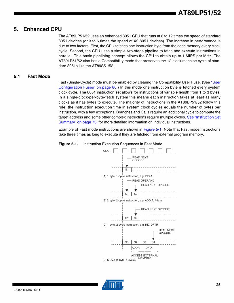
5.1 Fast ModeFast (Single-Cycle) mode must be enabled by clearing the Compatibility User Fuse. (See “UserConfiguration Fuses” on page 86.) In this mode one instruction byte is fetched every systemclock cycle. The 8051 instruction set allows for instructions of variable length from 1 to 3 bytes.In a single-clock-per-byte-fetch system this means each instruction takes at least as manyclocks as it has bytes to execute. The majority of instructions in the AT89LP51/52 follow thisrule: the instruction execution time in system clock cycles equals the number of bytes perinstruction, with a few exceptions. Branches and Calls require an additional cycle to compute thetarget address and some other complex instructions require multiple cycles. See “Instruction SetSummary” on page 75. for more detailed information on individual instructions.
Example of Fast mode instructions are shown in Figure 5-1. Note that Fast mode instructionstake three times as long to execute if they are fetched from external program memory.
Figure 5-1. Instruction Execution Sequences in Fast Mode
READ NEXTOPCODE
(A) 1-byte, 1-cycle instruction, e.g. INC A
S1
(B) 2-byte, 2-cycle instruction, e.g. ADD A, #data
S1 S2
READ NEXT OPCODE
READ OPERAND
(C) 1-byte, 2-cycle instruction, e.g. INC DPTR
S1 S2
READ NEXT OPCODE
(D) MOVX (1-byte, 4-cycle)
S1 S2 S3 S4
ADDR DATA
ACCESS EXTERNAL MEMORY
CLK
READ NEXTOPCODE
263709D–MICRO–12/11
AT89LP51/52
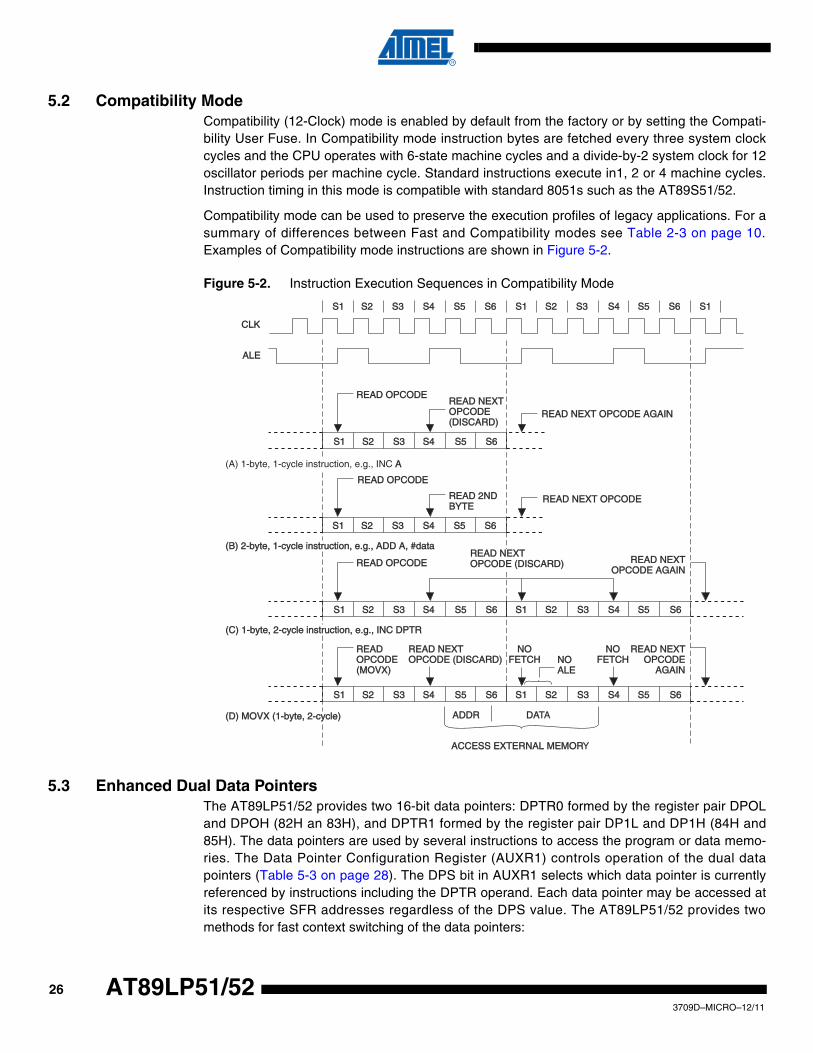
5.2 Compatibility ModeCompatibility (12-Clock) mode is enabled by default from the factory or by setting the Compati-bility User Fuse. In Compatibility mode instruction bytes are fetched every three system clockcycles and the CPU operates with 6-state machine cycles and a divide-by-2 system clock for 12oscillator periods per machine cycle. Standard instructions execute in1, 2 or 4 machine cycles.Instruction timing in this mode is compatible with standard 8051s such as the AT89S51/52.
Compatibility mode can be used to preserve the execution profiles of legacy applications. For asummary of differences between Fast and Compatibility modes see Table 2-3 on page 10.Examples of Compatibility mode instructions are shown in Figure 5-2.
Figure 5-2. Instruction Execution Sequences in Compatibility Mode
5.3 Enhanced Dual Data PointersThe AT89LP51/52 provides two 16-bit data pointers: DPTR0 formed by the register pair DPOLand DPOH (82H an 83H), and DPTR1 formed by the register pair DP1L and DP1H (84H and85H). The data pointers are used by several instructions to access the program or data memo-ries. The Data Pointer Configuration Register (AUXR1) controls operation of the dual datapointers (Table 5-3 on page 28). The DPS bit in AUXR1 selects which data pointer is currentlyreferenced by instructions including the DPTR operand. Each data pointer may be accessed atits respective SFR addresses regardless of the DPS value. The AT89LP51/52 provides twomethods for fast context switching of the data pointers:
S1S1 S2S2 S3S3 S4S4 S5S5 S6S6
S1S1 S2S2 S3S3 S4S4 S5S5 S6S6
S1S1 S2S2 S3S3 S4S4 S5S5 S6S6 S1S1 S2S2 S3S3 S4S4 S5S5 S6S6
S1S1 S2S2 S3S3 S4S4 S5S5 S6S6 S1S1 S2S2 S3S3 S4S4 S5S5 S6S6
S1S1 S2S2 S3S3 S4S4 S5S5 S6S6 S1S1 S2S2 S3S3 S4S4 S5S5 S6S6
S1S1
CLKCLK
ALEALE
READ OPCODEREAD OPCODE
(A) 1-byte, 1-cycle instruction, e.g., INC AA
(B) 2-byte, 1-cycle instruction, e.g., ADD A, #data(B) 2-byte, 1-cycle instruction, e.g., ADD A, #data
(C) 1-byte, 2-cycle instruction, e.g., INC DPTR(C) 1-byte, 2-cycle instruction, e.g., INC DPTR
(D) MOVX (1-byte, 2-cycle)(D) MOVX (1-byte, 2-cycle)
READ NEXTREAD NEXTOPCODEOPCODE(DISCARD)(DISCARD)
READ NEXT OPCODE AGAINREAD NEXT OPCODE AGAIN
READ OPCODEREAD OPCODE
READ 2NDREAD 2NDBYTEBYTE
READ NEXT OPCODEREAD NEXT OPCODE
READ OPCODEREAD OPCODE READ NEXTREAD NEXTOPCODE AGAINOPCODE AGAIN
READ READ OPCODEOPCODE(MOVX)(MOVX)
NO NO ALEALE
READ NEXTREAD NEXTOPCODE (DISCARD)OPCODE (DISCARD)
READ NEXTREAD NEXTOPCODE OPCODE
AGAINAGAIN
NONOFETCHFETCH
DADATA
ACCESS EXTERNAL MEMORACCESS EXTERNAL MEMORY
ADDRADDR
NONOFETCHFETCH
READ NEXTREAD NEXTOPCODE (DISCARD)OPCODE (DISCARD)
273709D–MICRO–12/11
AT89LP51/52
• Bit 2 of AUXR1 is hard-wired as a logic 0. The DPS bit may be toggled (to switch data pointers) simply by incrementing the AUXR1 register, without altering other bits in the register unintentionally. This is the preferred method when only a single data pointer will be used at one time.EX: INC AUXR1 ; Toggle DPS
• In some cases, both data pointers must be used simultaneously. To prevent frequent toggling of DPS, the AT89LP51/52 supports a prefix notation for selecting the opposite data pointer per instruction. All DPTR instructions, with the exception of JMP @A+DPTR, when prefixed with an 0A5H opcode will use the inverse value of DPS (DPS) to select the data pointer. Some assemblers may support this operation by using the /DPTR operand. For example, the following code performs a block copy within EDATA:
MOV AUXR1, #00H ; DPS = 0
MOV DPTR, #SRC ; load source address to dptr0
MOV /DPTR, #DST ; load destination address to dptr1
MOV R7, #BLKSIZE ; number of bytes to copy
COPY: MOVX A, @DPTR ; read source (dptr0)
INC DPTR ; next src (dptr0+1)
MOVX @/DPTR, A ; write destination (dptr1)
INC /DPTR ; next dst (dptr1+1)
DJNZ R7, COPY
For assemblers that do not support this notation, the 0A5H prefix must be declared in-line:
EX: DB 0A5H
INC DPTR ; equivalent to INC /DPTR
A summary of data pointer instructions with fast context switching is listed inTable 5-1.
5.3.1 Data Pointer UpdateThe Dual Data Pointers on the AT89LP51/52 include two features that control how the datapointers are updated. The data pointer decrement bits, DPD1 and DPD0 in AUXR1, configurethe INC DPTR instruction to act as DEC DPTR. The resulting operation will depend on DPS asshown in Table 5-2. These bits also control the direction of auto-updates during MOVC andMOVX.
Table 5-1. Data Pointer Instructions
Instruction
Operation
DPS = 0 DPS = 1
JMP @A+DPTR JMP @A+DPTR0 JMP @A+DPTR1
MOV DPTR, #data16 MOV DPTR0, #data16 MOV DPTR1, #data16
MOV /DPTR, #data16 MOV DPTR1, #data16 MOV DPTR0, #data16
INC DPTR INC DPTR0 INC DPTR1
INC /DPTR INC DPTR1 INC DPTR0
MOVC A,@A+DPTR MOVC A,@A+DPTR0 MOVC A,@A+DPTR1
MOVC A,@A+/DPTR MOVC A,@A+DPTR1 MOVC A,@A+DPTR0
MOVX A,@DPTR MOVX A,@DPTR0 MOVX A,@DPTR1
MOVX A,@/DPTR MOVX A,@DPTR1 MOVX A,@DPTR0
MOVX @DPTR, A MOVX @DPTR0, A MOVX @DPTR1, A
MOVX @/DPTR, A MOVX @DPTR1, A MOVX @DPTR0, A
283709D–MICRO–12/11
AT89LP51/52
The data pointer update bits, DPU1 and DPU0, allow MOVX @DPTR and MOVC @DPTRinstructions to update the selected data pointer automatically in a post-increment or post-decre-ment fashion. The direction of update depends on the DPD1 and DPD0 bits as shown in Table5-4. These bits can be used to make block copy routines more efficient.
Table 5-2. Data Pointer Decrement Behavior
DPD1 DPD0
Equivalent Operation for INC DPTR and INC /DPTR
DPS = 0 DPS = 1
INC DPTR INC /DPTR INC DPTR INC /DPTR
0 0 INC DPTR0 INC DPTR1 INC DPTR1 INC DPTR0
0 1 DEC DPTR0 INC DPTR1 INC DPTR1 DEC DPTR0
1 0 INC DPTR0 DEC DPTR1 DEC DPTR1 INC DPTR0
1 1 DEC DPTR0 DEC DPTR1 DEC DPTR1 DEC DPTR0
Table 5-3. AUXR1 – Data Pointer Configuration Register
AUXR1 = A2H Reset Value = 0000 00X0B
Not Bit Addressable
DPU1 DPU0 DPD1 DPD0 SIGEN 0 – DPS
Bit 7 6 5 4 3 2 1 0
Symbol Function
DPU1 Data Pointer 1 Update. When set, MOVX @DPTR and MOVC @DPTR instructions that use DPTR1 will also update DPTR1 based on DPD1. If DPD1 = 0 the operation is post-increment and if DPD1 = 1 the operation is post-decrement. When DPU1 = 0, DPTR1 is not updated.
DPU0 Data Pointer 0 Update. When set, MOVX @DPTR and MOVC @DPTR instructions that use DPTR0 will also update DPTR0 based on DPD0. If DPD0 = 0 the operation is post-increment and if DPD0 = 1 the operation is post-decrement. When DPU0 = 0, DPTR0 is not updated.
DPD1 Data Pointer 1 Decrement. When set, INC DPTR instructions targeted to DPTR1 will decrement DPTR1. When cleared, INC DPTR instructions will increment DPTR1. DPD1 also determines the direction of auto-update for DPTR1 when DPU1 = 1.
DPD0 Data Pointer 0 Decrement. When set, INC DPTR instructions targeted to DPTR0 will decrement DPTR0. When cleared, INC DPTR instructions will increment DPTR0. DPD0 also determines the direction of auto-update for DPTR0 when DPU0 = 1.
SIGEN Signature Enable. When SIGEN = 1 all MOVC @DPTR instructions and all IAP accesses will target the signature array memory. When SIGEN = 0, all MOVC and IAP accesses target CODE memory.
DPS Data Pointer Select. DPS selects the active data pointer for instructions that reference DPTR. When DPS = 0, DPTR will target DPTR0 and /DPTR will target DPTR1. When DPS = 1, DPTR will target DPTR1 and /DPTR will target DPTR0.
Table 5-4. Data Pointer Auto-Update
DPD1 DPD0
Update Operation for MOVX and MOVC (DPU1 = 1 & DPU0 = 1)
DPS = 0 DPS = 1
DPTR /DPTR DPTR /DPTR
0 0 DPTR0++ DPTR1++ DPTR1++ DPTR0++
0 1 DPTR0-- DPTR1++ DPTR1++ DPTR0--
1 0 DPTR0++ DPTR1-- DPTR1-- DPTR0++
1 1 DPTR0-- DPTR1-- DPTR1-- DPTR0--
293709D–MICRO–12/11
AT89LP51/52
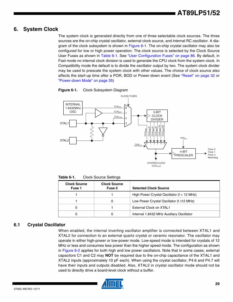
6. System ClockThe system clock is generated directly from one of three selectable clock sources. The threesources are the on-chip crystal oscillator, external clock source, and internal RC oscillator. A dia-gram of the clock subsystem is shown in Figure 6-1. The on-chip crystal oscillator may also beconfigured for low or high power operation. The clock source is selected by the Clock SourceUser Fuses as shown in Table 6-1. See “User Configuration Fuses” on page 86. By default, inFast mode no internal clock division is used to generate the CPU clock from the system clock. InCompatibility mode the default is to divide the oscillator output by two. The system clock dividermay be used to prescale the system clock with other values. The choice of clock source alsoaffects the start-up time after a POR, BOD or Power-down event (See “Reset” on page 32 or“Power-down Mode” on page 35)
Figure 6-1. Clock Subsystem Diagram
6.1 Crystal OscillatorWhen enabled, the internal inverting oscillator amplifier is connected between XTAL1 andXTAL2 for connection to an external quartz crystal or ceramic resonator. The oscillator mayoperate in either high-power or low-power mode. Low-speed mode is intended for crystals of 12MHz or less and consumes less power than the higher speed mode. The configuration as shownin Figure 6-2 applies for both high and low power oscillators. Note that in some cases, externalcapacitors C1 and C2 may NOT be required due to the on-chip capacitance of the XTAL1 andXTAL2 inputs (approximately 10 pF each). When using the crystal oscillator, P4.6 and P4.7 willhave their inputs and outputs disabled. Also, XTAL2 in crystal oscillator mode should not beused to directly drive a board-level clock without a buffer.
Table 6-1. Clock Source Settings
Clock SourceFuse 1
Clock Source Fuse 0 Selected Clock Source
1 1 High Power Crystal Oscillator (f > 12 MHz)
1 0 Low Power Crystal Oscillator (f ≤ 12 MHz)
0 1 External Clock on XTAL1
0 0 Internal 1.8432 MHz Auxiliary Oscillator
CLK
osc
XTAL1
XTAL2
SYSTEM CLOCK(CLKSYS)
INTERNAL1.8432MHz
OSC0
1
2
3
CLK
osc/
2
CLK
osc/
4
CLK
osc/
8
CLK
osc/
16
CLK
osc/
3 2
5-BITCLOCK
DIVIDER
CLKIRC
CLKEXT
CLKXTAL
0 1 2 3 4 5CDV2-0
CLOCK FUSES
4-BITPRESCALER
TPS3-0
Timer 0Timer 1Timer 2Watchdog
303709D–MICRO–12/11
AT89LP51/52
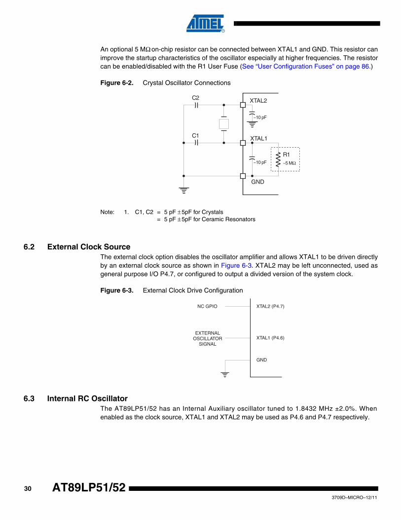
An optional 5 MΩ on-chip resistor can be connected between XTAL1 and GND. This resistor canimprove the startup characteristics of the oscillator especially at higher frequencies. The resistorcan be enabled/disabled with the R1 User Fuse (See “User Configuration Fuses” on page 86.)
Figure 6-2. Crystal Oscillator Connections
Note: 1. C1, C2 = 5 pF ± 5pF for Crystals= 5 pF ± 5pF for Ceramic Resonators
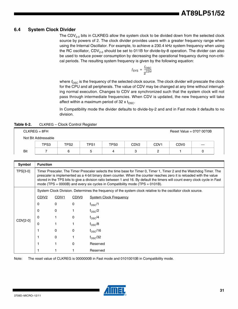
6.2 External Clock SourceThe external clock option disables the oscillator amplifier and allows XTAL1 to be driven directlyby an external clock source as shown in Figure 6-3. XTAL2 may be left unconnected, used asgeneral purpose I/O P4.7, or configured to output a divided version of the system clock.
Figure 6-3. External Clock Drive Configuration
6.3 Internal RC OscillatorThe AT89LP51/52 has an Internal Auxiliary oscillator tuned to 1.8432 MHz ±2.0%. Whenenabled as the clock source, XTAL1 and XTAL2 may be used as P4.6 and P4.7 respectively.
~10 pF
~10 pF
C2
C1
R1~5 MΩ
XT AL2 (P4.7)
XT AL1 (P4.6)
GND
NC GPIO
EXTERNAL OSCILLA T OR
SIGNAL
313709D–MICRO–12/11
AT89LP51/52
6.4 System Clock DividerThe CDV2-0 bits in CLKREG allow the system clock to be divided down from the selected clocksource by powers of 2. The clock divider provides users with a greater frequency range whenusing the Internal Oscillator. For example, to achieve a 230.4 kHz system frequency when usingthe RC oscillator, CDV2-0 should be set to 011B for divide-by-8 operation. The divider can alsobe used to reduce power consumption by decreasing the operational frequency during non-criti-cal periods. The resulting system frequency is given by the following equation:
where fOSC is the frequency of the selected clock source. The clock divider will prescale the clockfor the CPU and all peripherals. The value of CDV may be changed at any time without interrupt-ing normal execution. Changes to CDV are synchronized such that the system clock will notpass through intermediate frequencies. When CDV is updated, the new frequency will takeaffect within a maximum period of 32 x tOSC.
In Compatibility mode the divider defaults to divide-by-2 and and in Fast mode it defaults to nodivision.
Note: The reset value of CLKREG is 0000000B in Fast mode and 01010010B in Compatibility mode.
fSYSfOSC
2CDV-------------=
Table 6-2. CLKREG – Clock Control Register
CLKREG = 8FH Reset Value = 0?0? 00?0B
Not Bit Addressable
TPS3 TPS2 TPS1 TPS0 CDV2 CDV1 CDV0 —
Bit 7 6 5 4 3 2 1 0
Symbol Function
TPS[3-0] Timer Prescaler. The Timer Prescaler selects the time base for Timer 0, Timer 1, Timer 2 and the Watchdog Timer. The prescaler is implemented as a 4-bit binary down counter. When the counter reaches zero it is reloaded with the value stored in the TPS bits to give a division ratio between 1 and 16. By default the timers will count every clock cycle in Fast mode (TPS = 0000B) and every six cycles in Compatibility mode (TPS = 0101B).
CDV[2-0]
System Clock Division. Determines the frequency of the system clock relative to the oscillator clock source.
CDIV2 CDIV1 CDIV0 System Clock Frequency
0 0 0 fOSC/1
0 0 1 fOSC/2
0 1 0 fOSC/4
0 1 1 fOSC/8
1 0 0 fOSC/16
1 0 1 fOSC/32
1 1 0 Reserved
1 1 1 Reserved
323709D–MICRO–12/11
AT89LP51/52
7. ResetDuring reset, all I/O Registers are set to their initial values, the port pins are set to their defaultmode, and the program starts execution from the Reset Vector, 0000H. The AT89LP51/52 hasfive sources of reset: power-on reset, brown-out reset, external reset, watchdog reset, and soft-ware reset.
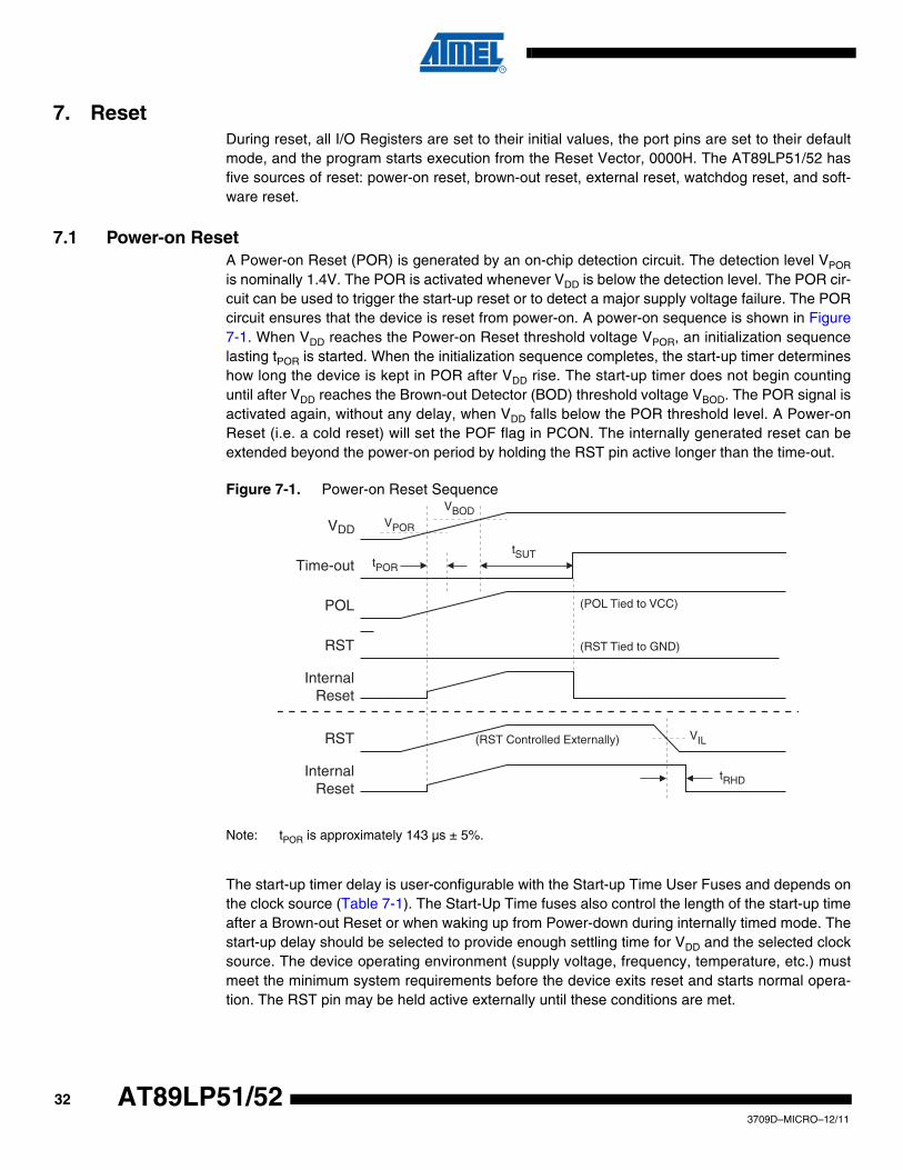
7.1 Power-on ResetA Power-on Reset (POR) is generated by an on-chip detection circuit. The detection level VPOR
is nominally 1.4V. The POR is activated whenever VDD is below the detection level. The POR cir-cuit can be used to trigger the start-up reset or to detect a major supply voltage failure. The PORcircuit ensures that the device is reset from power-on. A power-on sequence is shown in Figure7-1. When VDD reaches the Power-on Reset threshold voltage VPOR, an initialization sequencelasting tPOR is started. When the initialization sequence completes, the start-up timer determineshow long the device is kept in POR after VDD rise. The start-up timer does not begin countinguntil after VDD reaches the Brown-out Detector (BOD) threshold voltage VBOD. The POR signal isactivated again, without any delay, when VDD falls below the POR threshold level. A Power-onReset (i.e. a cold reset) will set the POF flag in PCON. The internally generated reset can beextended beyond the power-on period by holding the RST pin active longer than the time-out.
Figure 7-1. Power-on Reset Sequence
Note: tPOR is approximately 143 µs ± 5%.
The start-up timer delay is user-configurable with the Start-up Time User Fuses and depends onthe clock source (Table 7-1). The Start-Up Time fuses also control the length of the start-up timeafter a Brown-out Reset or when waking up from Power-down during internally timed mode. Thestart-up delay should be selected to provide enough settling time for VDD and the selected clocksource. The device operating environment (supply voltage, frequency, temperature, etc.) mustmeet the minimum system requirements before the device exits reset and starts normal opera-tion. The RST pin may be held active externally until these conditions are met.
VDD
RST
Time-out tPOR
tRHD
VPOR
InternalReset
RST
InternalReset
VIL
tSUT
VBOD
(RST Tied to GND)
(RST Controlled Externally)
POL (POL Tied to VCC)
333709D–MICRO–12/11
AT89LP51/52
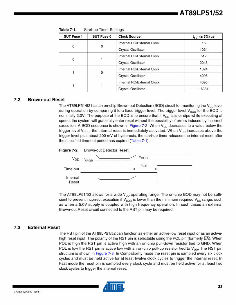
7.2 Brown-out ResetThe AT89LP51/52 has an on-chip Brown-out Detection (BOD) circuit for monitoring the VDD levelduring operation by comparing it to a fixed trigger level. The trigger level VBOD for the BOD isnominally 2.0V. The purpose of the BOD is to ensure that if VDD fails or dips while executing atspeed, the system will gracefully enter reset without the possibility of errors induced by incorrectexecution. A BOD sequence is shown in Figure 7-2. When VDD decreases to a value below thetrigger level VBOD, the internal reset is immediately activated. When VDD increases above thetrigger level plus about 200 mV of hysteresis, the start-up timer releases the internal reset afterthe specified time-out period has expired (Table 7-1).
Figure 7-2. Brown-out Detector Reset
The AT89LP51/52 allows for a wide VDD operating range. The on-chip BOD may not be suffi-cient to prevent incorrect execution if VBOD is lower than the minimum required VDD range, suchas when a 5.0V supply is coupled with high frequency operation. In such cases an externalBrown-out Reset circuit connected to the RST pin may be required.
7.3 External ResetThe RST pin of the AT89LP51/52 can function as either an active-low reset input or as an active-high reset input. The polarity of the RST pin is selectable using the POL pin (formerly EA). WhenPOL is high the RST pin is active high with an on-chip pull-down resistor tied to GND. WhenPOL is low the RST pin is active low with an on-chip pull-up resistor tied to VDD. The RST pinstructure is shown in Figure 7-3. In Compatibility mode the reset pin is sampled every six clockcycles and must be held active for at least twelve clock cycles to trigger the internal reset. InFast mode the reset pin is sampled every clock cycle and must be held active for at least twoclock cycles to trigger the internal reset.
Table 7-1. Start-up Timer Settings
SUT Fuse 1 SUT Fuse 0 Clock Source tSUT (± 5%) µs
0 0Internal RC/External Clock 16
Crystal Oscillator 1024
0 1Internal RC/External Clock 512
Crystal Oscillator 2048
1 0Internal RC/External Clock 1024
Crystal Oscillator 4096
1 1Internal RC/External Clock 4096
Crystal Oscillator 16384
VDD
Time-out
VPOR
InternalReset
tSUT
VBOD
343709D–MICRO–12/11
AT89LP51/52
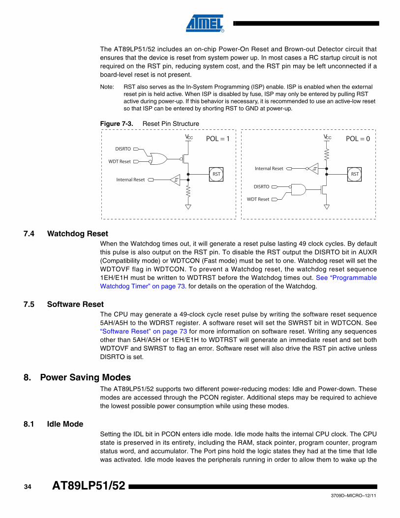
The AT89LP51/52 includes an on-chip Power-On Reset and Brown-out Detector circuit thatensures that the device is reset from system power up. In most cases a RC startup circuit is notrequired on the RST pin, reducing system cost, and the RST pin may be left unconnected if aboard-level reset is not present.
Note: RST also serves as the In-System Programming (ISP) enable. ISP is enabled when the external reset pin is held active. When ISP is disabled by fuse, ISP may only be entered by pulling RST active during power-up. If this behavior is necessary, it is recommended to use an active-low reset so that ISP can be entered by shorting RST to GND at power-up.
Figure 7-3. Reset Pin Structure
7.4 Watchdog ResetWhen the Watchdog times out, it will generate a reset pulse lasting 49 clock cycles. By defaultthis pulse is also output on the RST pin. To disable the RST output the DISRTO bit in AUXR(Compatibility mode) or WDTCON (Fast mode) must be set to one. Watchdog reset will set theWDTOVF flag in WDTCON. To prevent a Watchdog reset, the watchdog reset sequence1EH/E1H must be written to WDTRST before the Watchdog times out. See “ProgrammableWatchdog Timer” on page 73. for details on the operation of the Watchdog.
7.5 Software ResetThe CPU may generate a 49-clock cycle reset pulse by writing the software reset sequence5AH/A5H to the WDRST register. A software reset will set the SWRST bit in WDTCON. See“Software Reset” on page 73 for more information on software reset. Writing any sequencesother than 5AH/A5H or 1EH/E1H to WDTRST will generate an immediate reset and set bothWDTOVF and SWRST to flag an error. Software reset will also drive the RST pin active unlessDISRTO is set.
8. Power Saving ModesThe AT89LP51/52 supports two different power-reducing modes: Idle and Power-down. Thesemodes are accessed through the PCON register. Additional steps may be required to achievethe lowest possible power consumption while using these modes.
8.1 Idle ModeSetting the IDL bit in PCON enters idle mode. Idle mode halts the internal CPU clock. The CPUstate is preserved in its entirety, including the RAM, stack pointer, program counter, programstatus word, and accumulator. The Port pins hold the logic states they had at the time that Idlewas activated. Idle mode leaves the peripherals running in order to allow them to wake up the
VCC
DISRTO
WDT Reset
RSTInternal Reset
POL = 1 VCC
DISRTO
WDT Reset
RSTInternal Reset
POL = 0
353709D–MICRO–12/11
AT89LP51/52
CPU when an interrupt is generated. The timer and UART peripherals continue to function dur-ing Idle. If these functions are not needed during idle, they should be explicitly disabled byclearing the appropriate control bits in their respective SFRs. The watchdog may be selectivelyenabled or disabled during Idle by setting/clearing the WDIDLE bit. The Brown-out Detector isalways active during Idle. Any enabled interrupt source or reset may terminate Idle mode. Whenexiting Idle mode with an interrupt, the interrupt will immediately be serviced, and following RETIthe next instruction to be executed will be the one following the instruction that put the deviceinto Idle.
The power consumption during Idle mode can be further reduced by prescaling down the systemclock using the System Clock Divider (Section 6.4 on page 31). Be aware that the clock dividerwill affect all peripheral functions and baud rates may need to be adjusted to maintain their ratewith the new clock frequency..
8.2 Power-down ModeSetting the Power-down (PD) bit in PCON enters Power-down mode. Power-down mode stopsthe oscillator, disables the BOD and powers down the Flash memory in order to minimize powerconsumption. Only the power-on circuitry will continue to draw power during Power-down. Dur-ing Power-down, the power supply voltage may be reduced to the RAM keep-alive voltage. TheRAM contents will be retained, but the SFR contents are not guaranteed once VDD has beenreduced. Power-down may be exited by external reset, power-on reset, or certain enabledinterrupts.
Table 8-1. PCON – Power Control Register
PCON = 87H Reset Value = 000X 0000B
Not Bit Addressable
SMOD1 SMOD0 PWDEX POF GF1 GF0 PD IDL
Bit 7 6 5 4 3 2 1 0
Symbol Function
SMOD1 Double Baud Rate bit. Doubles the baud rate of the UART in Modes 1, 2, or 3.
SMOD0 Frame Error Select. When SMOD0 = 1, SCON.7 is SM0. When SMOD0 = 1, SCON.7 is FE. Note that FE will be set after a frame error regardless of the state of SMOD0.
PWDEX Power-down Exit Mode. When PWDEX = 0, wake up from Power-down is externally controlled. When PWDEX = 1, wake up from Power-down is internally timed.
POF Power Off Flag. POF is set to “1” during power up (i.e. cold reset). It can be set or reset under software control and is not affected by RST or BOD (i.e. warm resets).
GF1, GF0 General-purpose Flags
PD Power-down bit. Setting this bit activates power-down operation. The PD bit is cleared automatically by hardware when waking up from power-down.
IDL Idle Mode bit. Setting this bit activates Idle mode operation. The IDL bit is cleared automatically by hardware when waking up from idle
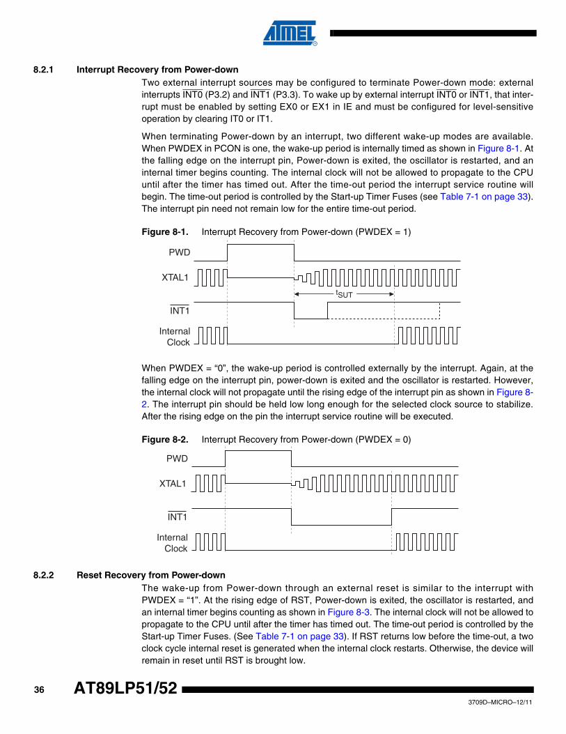
363709D–MICRO–12/11
AT89LP51/52
8.2.1 Interrupt Recovery from Power-down Two external interrupt sources may be configured to terminate Power-down mode: externalinterrupts INT0 (P3.2) and INT1 (P3.3). To wake up by external interrupt INT0 or INT1, that inter-rupt must be enabled by setting EX0 or EX1 in IE and must be configured for level-sensitiveoperation by clearing IT0 or IT1.
When terminating Power-down by an interrupt, two different wake-up modes are available.When PWDEX in PCON is one, the wake-up period is internally timed as shown in Figure 8-1. Atthe falling edge on the interrupt pin, Power-down is exited, the oscillator is restarted, and aninternal timer begins counting. The internal clock will not be allowed to propagate to the CPUuntil after the timer has timed out. After the time-out period the interrupt service routine willbegin. The time-out period is controlled by the Start-up Timer Fuses (see Table 7-1 on page 33).The interrupt pin need not remain low for the entire time-out period.
Figure 8-1. Interrupt Recovery from Power-down (PWDEX = 1)
When PWDEX = “0”, the wake-up period is controlled externally by the interrupt. Again, at thefalling edge on the interrupt pin, power-down is exited and the oscillator is restarted. However,the internal clock will not propagate until the rising edge of the interrupt pin as shown in Figure 8-2. The interrupt pin should be held low long enough for the selected clock source to stabilize.After the rising edge on the pin the interrupt service routine will be executed.
Figure 8-2. Interrupt Recovery from Power-down (PWDEX = 0)
8.2.2 Reset Recovery from Power-downThe wake-up from Power-down through an external reset is similar to the interrupt withPWDEX = “1”. At the rising edge of RST, Power-down is exited, the oscillator is restarted, andan internal timer begins counting as shown in Figure 8-3. The internal clock will not be allowed topropagate to the CPU until after the timer has timed out. The time-out period is controlled by theStart-up Timer Fuses. (See Table 7-1 on page 33). If RST returns low before the time-out, a twoclock cycle internal reset is generated when the internal clock restarts. Otherwise, the device willremain in reset until RST is brought low.
PWD
INT1
XTAL1
tSUT
InternalClock
PWD
INT1
XTAL1
InternalClock
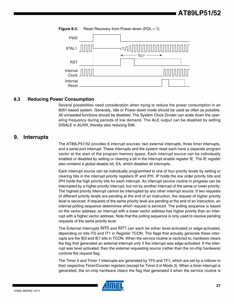
373709D–MICRO–12/11
AT89LP51/52
Figure 8-3. Reset Recovery from Power-down (POL = 1)
8.3 Reducing Power ConsumptionSeveral possibilities need consideration when trying to reduce the power consumption in an8051-based system. Generally, Idle or Power-down mode should be used as often as possible.All unneeded functions should be disabled. The System Clock Divider can scale down the oper-ating frequency during periods of low demand. The ALE output can be disabled by settingDISALE in AUXR, thereby also reducing EMI.
9. InterruptsThe AT89LP51/52 provides 6 interrupt sources: two external interrupts, three timer interrupts,and a serial port interrupt. These interrupts and the system reset each have a separate programvector at the start of the program memory space. Each interrupt source can be individuallyenabled or disabled by setting or clearing a bit in the interrupt enable register IE. The IE registeralso contains a global disable bit, EA, which disables all interrupts.
Each interrupt source can be individually programmed to one of four priority levels by setting orclearing bits in the interrupt priority registers IP and IPH. IP holds the low order priority bits andIPH holds the high priority bits for each interrupt. An interrupt service routine in progress can beinterrupted by a higher priority interrupt, but not by another interrupt of the same or lower priority.The highest priority interrupt cannot be interrupted by any other interrupt source. If two requestsof different priority levels are pending at the end of an instruction, the request of higher prioritylevel is serviced. If requests of the same priority level are pending at the end of an instruction, aninternal polling sequence determines which request is serviced. The polling sequence is basedon the vector address; an interrupt with a lower vector address has higher priority than an inter-rupt with a higher vector address. Note that the polling sequence is only used to resolve pendingrequests of the same priority level.
The External Interrupts INT0 and INT1 can each be either level-activated or edge-activated,depending on bits IT0 and IT1 in Register TCON. The flags that actually generate these inter-rupts are the IE0 and IE1 bits in TCON. When the service routine is vectored to, hardware clearsthe flag that generated an external interrupt only if the interrupt was edge-activated. If the inter-rupt was level activated, then the external requesting source (rather than the on-chip hardware)controls the request flag.
The Timer 0 and Timer 1 Interrupts are generated by TF0 and TF1, which are set by a rollover intheir respective Timer/Counter registers (except for Timer 0 in Mode 3). When a timer interrupt isgenerated, the on-chip hardware clears the flag that generated it when the service routine is
PWD
RST
XTAL1
tSUT
Internal Clock
Internal Reset
383709D–MICRO–12/11
AT89LP51/52
vectored to. The Timer 2 Interrupt is generated by a logic OR of bits TF2 and EXF2 in registerT2CON. Neither of these flags is cleared by hardware when the CPU vectors to the service rou-tine. The service routine normally must determine whether TF2 or EXF2 generated the interruptand that bit must be cleared by software.
The Serial Port Interrupt is generated by the logic OR of RI and TI in SCON. Neither of theseflags is cleared by hardware when the CPU vectors to the service routine. The service routinenormally must determine whether RI or TI generated the interrupt and that bit must be cleared bysoftware.
All of the bits that generate interrupts can be set or cleared by software, with the same result asthough they had been set or cleared by hardware. That is, interrupts can be generated andpending interrupts can be canceled in software.
9.1 Interrupt Response TimeThe interrupt flags may be set by their hardware in any clock cycle. The interrupt controller pollsthe flags in the last clock cycle of the instruction in progress. If one of the flags was set in thepreceding cycle, the polling cycle will find it and the interrupt system will generate an LCALL tothe appropriate service routine as the next instruction, provided that the interrupt is not blockedby any of the following conditions: an interrupt of equal or higher priority level is already in prog-ress; the instruction in progress is RETI or any write to the IE, IP or IPH registers; the CPU iscurrently forced into idle by an IAP or FDATA write. Each of these conditions will block the gen-eration of the LCALL to the interrupt service routine. The second condition ensures that if theinstruction in progress is RETI or any access to IE, IP or IPH, then at least one more instructionwill be executed before any interrupt is vectored to. The polling cycle is repeated at the last cycleof each instruction, and the values polled are the values that were present at the previous clockcycle. If an active interrupt flag is not being serviced because of one of the above conditions andis no longer active when the blocking condition is removed, the denied interrupt will not be ser-viced. In other words, the fact that the interrupt flag was once active but not serviced is notremembered. Every polling cycle is new.
If a request is active and conditions are met for it to be acknowledged, a hardware subroutinecall to the requested service routine will be the next instruction executed. The call itself takesfour cycles. Thus, a minimum of five complete clock cycles elapsed between activation of aninterrupt request and the beginning of execution of the first instruction of the service routine. Alonger response time results if the request is blocked by one of the previously listed conditions. Ifan interrupt of equal or higher priority level is already in progress, the additional wait timedepends on the nature of the other interrupt's service routine. If the instruction in progress is notin its final clock cycle, the additional wait time cannot be more than 4 cycles, since the longest
Table 9-1. Interrupt Vector Addresses
Interrupt Source Vector Address
System Reset RST or POR or BOD 0000H
External Interrupt 0 IE0 0003H
Timer 0 Overflow TF0 000BH
External Interrupt 1 IE1 0013H
Timer 1 Overflow TF1 001BH
Serial Port Interrupt RI or TI 0023H
Timer 2 Interrupt TF2 or EXF2 002BH
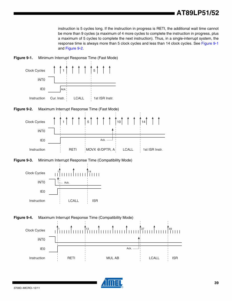
393709D–MICRO–12/11
AT89LP51/52
instruction is 5 cycles long. If the instruction in progress is RETI, the additional wait time cannotbe more than 9 cycles (a maximum of 4 more cycles to complete the instruction in progress, plusa maximum of 5 cycles to complete the next instruction). Thus, in a single-interrupt system, theresponse time is always more than 5 clock cycles and less than 14 clock cycles. See Figure 9-1and Figure 9-2.
Figure 9-1. Minimum Interrupt Response Time (Fast Mode)
Figure 9-2. Maximum Interrupt Response Time (Fast Mode)
Figure 9-3. Minimum Interrupt Response Time (Compatibility Mode)
Figure 9-4. Maximum Interrupt Response Time (Compatibility Mode)
Clock Cycles
INT0
IE0
1 5
Instruction LCALL 1st ISR Instr.Cur. Instr.
Ack.
Clock Cycles
INT0
IE0
1 14
Instruction RETI MOVX @/DPTR, A LCALL 1st ISR Instr.
Ack.
5 10
Clock Cycles
INT0
IE0
1
Instruction LCALL ISR
Ack.
14
Clock Cycles
INT0
IE0
1
Instruction RETI MUL AB LCALL ISR
Ack.
13 37 49
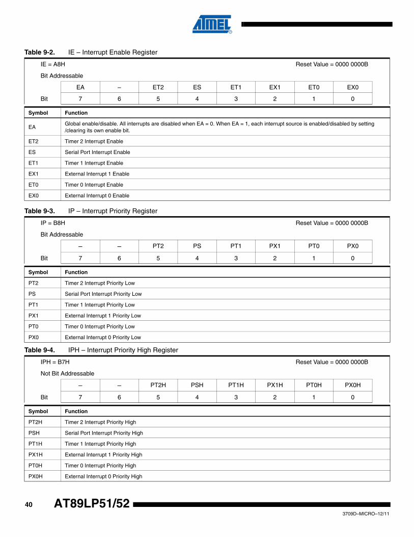
403709D–MICRO–12/11
AT89LP51/52
Table 9-2. IE – Interrupt Enable Register
IE = A8H Reset Value = 0000 0000B
Bit Addressable
EA – ET2 ES ET1 EX1 ET0 EX0
Bit 7 6 5 4 3 2 1 0
Symbol Function
EAGlobal enable/disable. All interrupts are disabled when EA = 0. When EA = 1, each interrupt source is enabled/disabled by setting /clearing its own enable bit.
ET2 Timer 2 Interrupt Enable
ES Serial Port Interrupt Enable
ET1 Timer 1 Interrupt Enable
EX1 External Interrupt 1 Enable
ET0 Timer 0 Interrupt Enable
EX0 External Interrupt 0 Enable
Table 9-3. IP – Interrupt Priority Register
IP = B8H Reset Value = 0000 0000B
Bit Addressable
– – PT2 PS PT1 PX1 PT0 PX0
Bit 7 6 5 4 3 2 1 0
Symbol Function
PT2 Timer 2 Interrupt Priority Low
PS Serial Port Interrupt Priority Low
PT1 Timer 1 Interrupt Priority Low
PX1 External Interrupt 1 Priority Low
PT0 Timer 0 Interrupt Priority Low
PX0 External Interrupt 0 Priority Low
Table 9-4. IPH – Interrupt Priority High Register
IPH = B7H Reset Value = 0000 0000B
Not Bit Addressable
– – PT2H PSH PT1H PX1H PT0H PX0H
Bit 7 6 5 4 3 2 1 0
Symbol Function
PT2H Timer 2 Interrupt Priority High
PSH Serial Port Interrupt Priority High
PT1H Timer 1 Interrupt Priority High
PX1H External Interrupt 1 Priority High
PT0H Timer 0 Interrupt Priority High
PX0H External Interrupt 0 Priority High
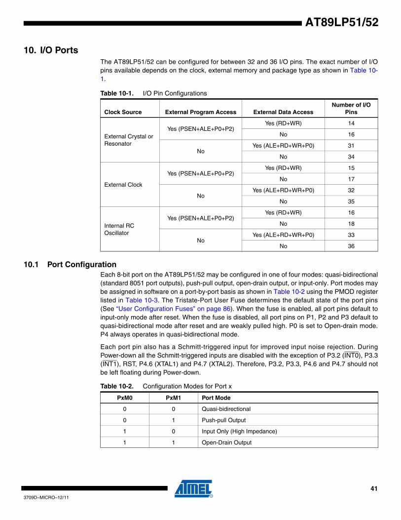
413709D–MICRO–12/11
AT89LP51/52
10. I/O PortsThe AT89LP51/52 can be configured for between 32 and 36 I/O pins. The exact number of I/Opins available depends on the clock, external memory and package type as shown in Table 10-1.
10.1 Port ConfigurationEach 8-bit port on the AT89LP51/52 may be configured in one of four modes: quasi-bidirectional(standard 8051 port outputs), push-pull output, open-drain output, or input-only. Port modes maybe assigned in software on a port-by-port basis as shown in Table 10-2 using the PMOD registerlisted in Table 10-3. The Tristate-Port User Fuse determines the default state of the port pins(See “User Configuration Fuses” on page 86). When the fuse is enabled, all port pins default toinput-only mode after reset. When the fuse is disabled, all port pins on P1, P2 and P3 default toquasi-bidirectional mode after reset and are weakly pulled high. P0 is set to Open-drain mode.P4 always operates in quasi-bidirectional mode.
Each port pin also has a Schmitt-triggered input for improved input noise rejection. DuringPower-down all the Schmitt-triggered inputs are disabled with the exception of P3.2 (INT0), P3.3(INT1), RST, P4.6 (XTAL1) and P4.7 (XTAL2). Therefore, P3.2, P3.3, P4.6 and P4.7 should notbe left floating during Power-down. .
Table 10-1. I/O Pin Configurations
Clock Source External Program Access External Data AccessNumber of I/O
Pins
External Crystal or Resonator
Yes (PSEN+ALE+P0+P2)Yes (RD+WR) 14
No 16
NoYes (ALE+RD+WR+P0) 31
No 34
External Clock
Yes (PSEN+ALE+P0+P2)Yes (RD+WR) 15
No 17
NoYes (ALE+RD+WR+P0) 32
No 35
Internal RC Oscillator
Yes (PSEN+ALE+P0+P2)Yes (RD+WR) 16
No 18
NoYes (ALE+RD+WR+P0) 33
No 36
Table 10-2. Configuration Modes for Port x
PxM0 PxM1 Port Mode
0 0 Quasi-bidirectional
0 1 Push-pull Output
1 0 Input Only (High Impedance)
1 1 Open-Drain Output
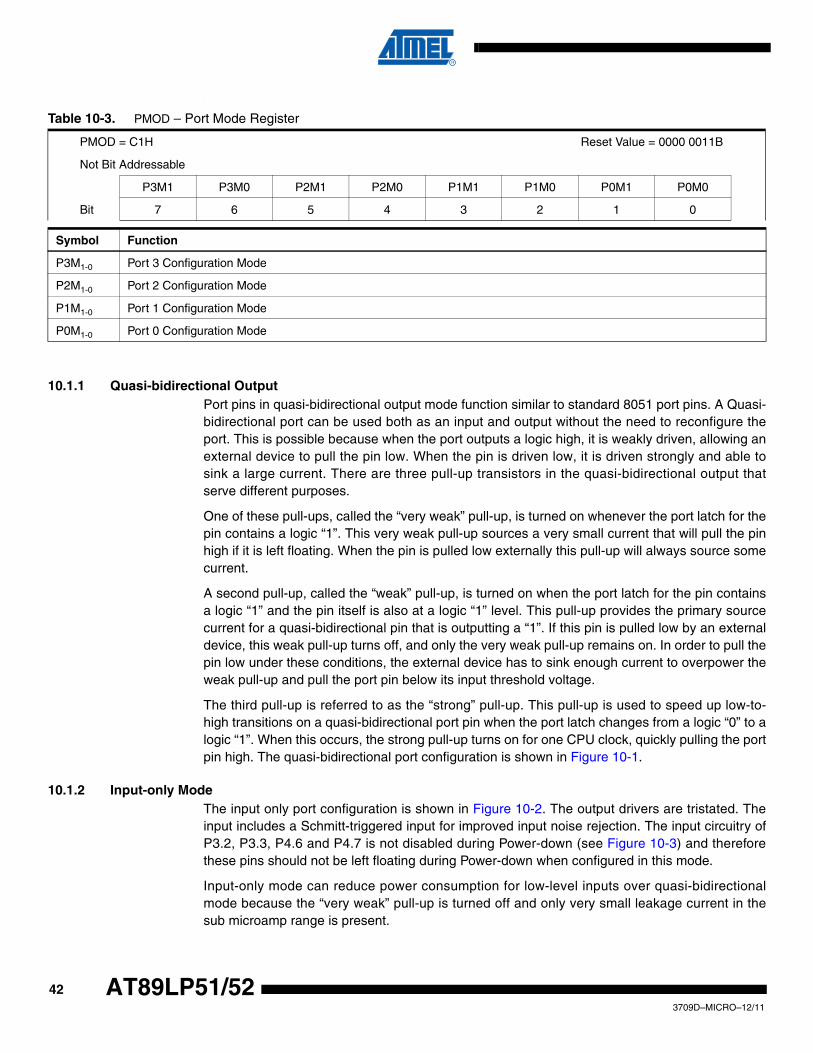
423709D–MICRO–12/11
AT89LP51/52
.
10.1.1 Quasi-bidirectional OutputPort pins in quasi-bidirectional output mode function similar to standard 8051 port pins. A Quasi-bidirectional port can be used both as an input and output without the need to reconfigure theport. This is possible because when the port outputs a logic high, it is weakly driven, allowing anexternal device to pull the pin low. When the pin is driven low, it is driven strongly and able tosink a large current. There are three pull-up transistors in the quasi-bidirectional output thatserve different purposes.
One of these pull-ups, called the “very weak” pull-up, is turned on whenever the port latch for thepin contains a logic “1”. This very weak pull-up sources a very small current that will pull the pinhigh if it is left floating. When the pin is pulled low externally this pull-up will always source somecurrent.
A second pull-up, called the “weak” pull-up, is turned on when the port latch for the pin containsa logic “1” and the pin itself is also at a logic “1” level. This pull-up provides the primary sourcecurrent for a quasi-bidirectional pin that is outputting a “1”. If this pin is pulled low by an externaldevice, this weak pull-up turns off, and only the very weak pull-up remains on. In order to pull thepin low under these conditions, the external device has to sink enough current to overpower theweak pull-up and pull the port pin below its input threshold voltage.
The third pull-up is referred to as the “strong” pull-up. This pull-up is used to speed up low-to-high transitions on a quasi-bidirectional port pin when the port latch changes from a logic “0” to alogic “1”. When this occurs, the strong pull-up turns on for one CPU clock, quickly pulling the portpin high. The quasi-bidirectional port configuration is shown in Figure 10-1.
10.1.2 Input-only ModeThe input only port configuration is shown in Figure 10-2. The output drivers are tristated. Theinput includes a Schmitt-triggered input for improved input noise rejection. The input circuitry ofP3.2, P3.3, P4.6 and P4.7 is not disabled during Power-down (see Figure 10-3) and thereforethese pins should not be left floating during Power-down when configured in this mode.
Input-only mode can reduce power consumption for low-level inputs over quasi-bidirectionalmode because the “very weak” pull-up is turned off and only very small leakage current in thesub microamp range is present.
Table 10-3. PMOD – Port Mode Register
PMOD = C1H Reset Value = 0000 0011B
Not Bit Addressable
P3M1 P3M0 P2M1 P2M0 P1M1 P1M0 P0M1 P0M0
Bit 7 6 5 4 3 2 1 0
Symbol Function
P3M1-0 Port 3 Configuration Mode
P2M1-0 Port 2 Configuration Mode
P1M1-0 Port 1 Configuration Mode
P0M1-0 Port 0 Configuration Mode
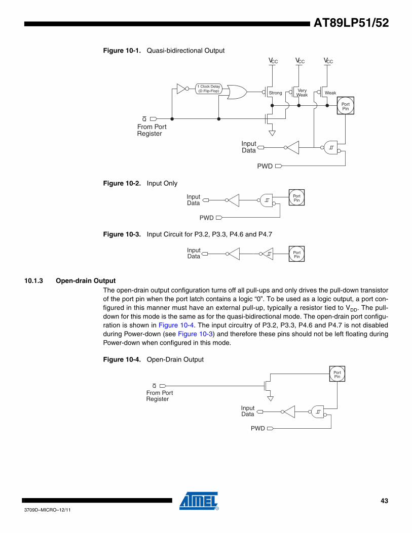
433709D–MICRO–12/11
AT89LP51/52
Figure 10-1. Quasi-bidirectional Output
Figure 10-2. Input Only
Figure 10-3. Input Circuit for P3.2, P3.3, P4.6 and P4.7
10.1.3 Open-drain OutputThe open-drain output configuration turns off all pull-ups and only drives the pull-down transistorof the port pin when the port latch contains a logic “0”. To be used as a logic output, a port con-figured in this manner must have an external pull-up, typically a resistor tied to VDD. The pull-down for this mode is the same as for the quasi-bidirectional mode. The open-drain port configu-ration is shown in Figure 10-4. The input circuitry of P3.2, P3.3, P4.6 and P4.7 is not disabledduring Power-down (see Figure 10-3) and therefore these pins should not be left floating duringPower-down when configured in this mode.
Figure 10-4. Open-Drain Output
1 Clo c k Del a y (D Flip-Flop) Strong V e r y
W ea k W ea k
P o r t Pin
V CC V CC V CC
F rom P o r t Register
Input Data
PWD
P o r t Pin
Input Data
PWD
PortPin
InputData
P o r t Pin
F rom P o r t Register
Input Data
PWD
443709D–MICRO–12/11
AT89LP51/52
10.1.4 Push-pull OutputThe push-pull output configuration has the same pull-down structure as both the open-drain andthe quasi-bidirectional output modes, but provides a continuous strong pull-up when the portlatch contains a logic “1”. The push-pull mode may be used when more source current is neededfrom a port output. The push-pull port configuration is shown in Figure 10-5.
Figure 10-5. Push-pull Output
10.2 Port Read-Modify-Write A read from a port will read either the state of the pins or the state of the port register dependingon which instruction is used. Simple read instructions will always access the port pins directly.Read-modify-write instructions, which read a value, possibly modify it, and then write it back, willalways access the port register. This includes bit write instructions such as CLR or SETB as theyactually read the entire port, modify a single bit, then write the data back to the entire port. SeeTable 10-4 for a complete list of Read-Modify-Write instruction which may access the ports.
P o r t Pin
V CC
F rom P o r t Register
Input Data
PWD
Table 10-4. Port Read-Modify-Write Instructions
Mnemonic Instruction Example
ANL Logical AND ANL P1, A
ORL Logical OR ORL P1, A
XRL Logical EX-OR XRL P1, A
JBC Jump if bit set and clear bit JBC P3.0, LABEL
CPL Complement bit CPL P3.1
INC Increment INC P1
DEC Decrement DEC P3
DJNZ Decrement and jump if not zero DJNZ P3, LABEL
MOV PX.Y, C Move carry to bit Y of Port X MOV P1.0, C
CLR PX.Y Clear bit Y of Port X CLR P1.1
SETB PX.Y Set bit Y of Port X SETB P3.2
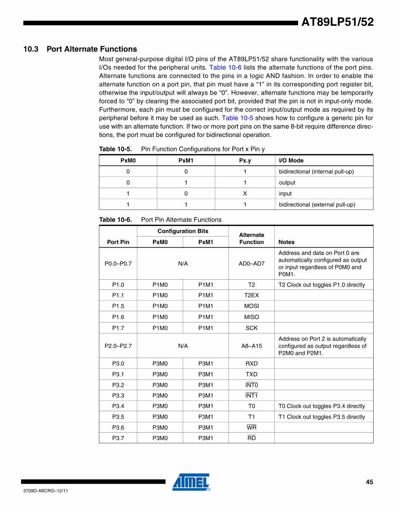
453709D–MICRO–12/11
AT89LP51/52
10.3 Port Alternate FunctionsMost general-purpose digital I/O pins of the AT89LP51/52 share functionality with the variousI/Os needed for the peripheral units. Table 10-6 lists the alternate functions of the port pins.Alternate functions are connected to the pins in a logic AND fashion. In order to enable thealternate function on a port pin, that pin must have a “1” in its corresponding port register bit,otherwise the input/output will always be “0”. However, alternate functions may be temporarilyforced to “0” by clearing the associated port bit, provided that the pin is not in input-only mode.Furthermore, each pin must be configured for the correct input/output mode as required by itsperipheral before it may be used as such. Table 10-5 shows how to configure a generic pin foruse with an alternate function. If two or more port pins on the same 8-bit require difference direc-tions, the port must be configured for bidirectional operation.
Table 10-5. Pin Function Configurations for Port x Pin y
PxM0 PxM1 Px.y I/O Mode
0 0 1 bidirectional (internal pull-up)
0 1 1 output
1 0 X input
1 1 1 bidirectional (external pull-up)
Table 10-6. Port Pin Alternate Functions
Port Pin
Configuration BitsAlternateFunction NotesPxM0 PxM1
P0.0–P0.7 N/A AD0–AD7
Address and data on Port 0 are automatically configured as output or input regardless of P0M0 and P0M1.
P1.0 P1M0 P1M1 T2 T2 Clock out toggles P1.0 directly
P1.1 P1M0 P1M1 T2EX
P1.5 P1M0 P1M1 MOSI
P1.6 P1M0 P1M1 MISO
P1.7 P1M0 P1M1 SCK
P2.0–P2.7 N/A A8–A15Address on Port 2 is automatically configured as output regardless of P2M0 and P2M1.
P3.0 P3M0 P3M1 RXD
P3.1 P3M0 P3M1 TXD
P3.2 P3M0 P3M1 INT0
P3.3 P3M0 P3M1 INT1
P3.4 P3M0 P3M1 T0 T0 Clock out toggles P3.4 directly
P3.5 P3M0 P3M1 T1 T1 Clock out toggles P3.5 directly
P3.6 P3M0 P3M1 WR
P3.7 P3M0 P3M1 RD
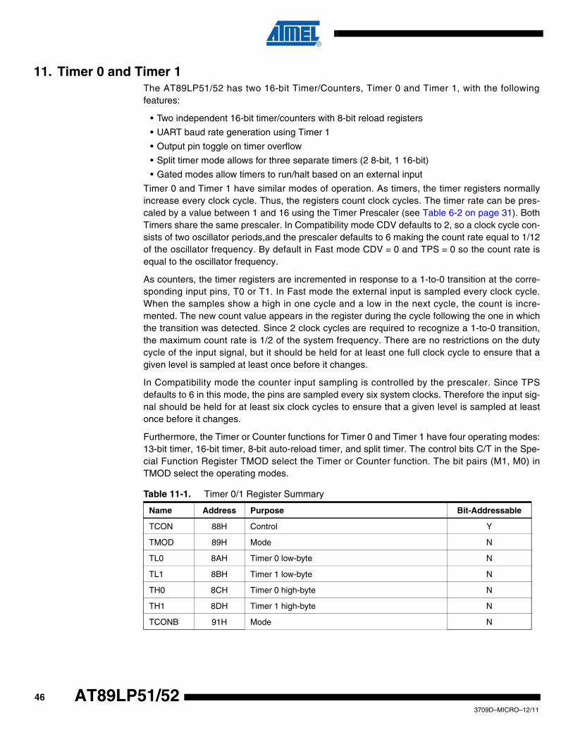
463709D–MICRO–12/11
AT89LP51/52
11. Timer 0 and Timer 1The AT89LP51/52 has two 16-bit Timer/Counters, Timer 0 and Timer 1, with the followingfeatures:
• Two independent 16-bit timer/counters with 8-bit reload registers
• UART baud rate generation using Timer 1
• Output pin toggle on timer overflow
• Split timer mode allows for three separate timers (2 8-bit, 1 16-bit)
• Gated modes allow timers to run/halt based on an external input
Timer 0 and Timer 1 have similar modes of operation. As timers, the timer registers normallyincrease every clock cycle. Thus, the registers count clock cycles. The timer rate can be pres-caled by a value between 1 and 16 using the Timer Prescaler (see Table 6-2 on page 31). BothTimers share the same prescaler. In Compatibility mode CDV defaults to 2, so a clock cycle con-sists of two oscillator periods,and the prescaler defaults to 6 making the count rate equal to 1/12of the oscillator frequency. By default in Fast mode CDV = 0 and TPS = 0 so the count rate isequal to the oscillator frequency.
As counters, the timer registers are incremented in response to a 1-to-0 transition at the corre-sponding input pins, T0 or T1. In Fast mode the external input is sampled every clock cycle.When the samples show a high in one cycle and a low in the next cycle, the count is incre-mented. The new count value appears in the register during the cycle following the one in whichthe transition was detected. Since 2 clock cycles are required to recognize a 1-to-0 transition,the maximum count rate is 1/2 of the system frequency. There are no restrictions on the dutycycle of the input signal, but it should be held for at least one full clock cycle to ensure that agiven level is sampled at least once before it changes.
In Compatibility mode the counter input sampling is controlled by the prescaler. Since TPSdefaults to 6 in this mode, the pins are sampled every six system clocks. Therefore the input sig-nal should be held for at least six clock cycles to ensure that a given level is sampled at leastonce before it changes.
Furthermore, the Timer or Counter functions for Timer 0 and Timer 1 have four operating modes:13-bit timer, 16-bit timer, 8-bit auto-reload timer, and split timer. The control bits C/T in the Spe-cial Function Register TMOD select the Timer or Counter function. The bit pairs (M1, M0) inTMOD select the operating modes.
Table 11-1. Timer 0/1 Register Summary
Name Address Purpose Bit-Addressable
TCON 88H Control Y
TMOD 89H Mode N
TL0 8AH Timer 0 low-byte N
TL1 8BH Timer 1 low-byte N
TH0 8CH Timer 0 high-byte N
TH1 8DH Timer 1 high-byte N
TCONB 91H Mode N
473709D–MICRO–12/11
AT89LP51/52
11.1 Mode 0 – 13-bit Timer/CounterBoth Timers in Mode 0 are 8-bit Counters with a divide-by-32 prescaler. Figure 11-1 shows theMode 0 operation as it applies to Timer 1. As the count rolls over from all “1”s to all “0”s, it setsthe Timer interrupt flag TF1. The counter input is enabled to the Timer when TR1 = 1 and eitherGATE1 = 0 or INT1 = 1. Setting GATE1 = 1 allows the Timer to be controlled by external inputINT1, to facilitate pulse width measurements. TR1 is a control bit in the Special Function Regis-ter TCON. GATE1 is in TMOD. The 13-bit register consists of all 8 bits of TH1 and the lower 5bits of TL1. The upper 3 bits of TL1 are indeterminate and should be ignored. Setting the run flag(TR1) does not clear the registers.
Figure 11-1. Timer/Counter 1 Mode 0: 13-bit Counter
Mode 0 operation is the same for Timer 0 as for Timer 1, except that TR0, TF0, GATE0 andINT0 replace the corresponding Timer 1 signals in Figure 11-1. There are two different C/T bits,one for Timer 1 (TMOD.6) and one for Timer 0 (TMOD.2).
11.2 Mode 1 – 16-bit Timer/CounterIn Mode 1 the Timers are configured for 16-bit operation. The Timer register is run with all 16 bitsand the clock is applied to the combined high and low timer registers (TH1/TL1). As clock pulsesare received, the timer counts up: 0000H, 0001H, 0002H, etc. An overflow occurs on theFFFFH-to-0000H transition, upon which the overflow flag bit in TCON is set. See Figure 11-2.Mode 1 operation is the same for Timer/Counter 0.
Figure 11-2. Timer/Counter 1 Mode 1: 16-bit Counter
Mode 0: Time-out Period8192
System Frequency-------------------------------------------------- TPS 1+( )×=
OSC
T1 Pin
TR1
GATE1
INT1 Pin
TL1 (5 Bits)
Control
Interrupt
C/T = 0
C/T = 1
TH1(8 Bits) TF1
÷CDV ÷TPS
Mode 1: Time-out Period65536
System Frequency-------------------------------------------------- TPS 1+( )×=
OSC
T1 Pin
TR1
GATE1
INT1 Pin
TL1 (8 Bits)
Control
Inter r up t
C/T = 0
C/T =1
TH1 (8 Bits) TF1
÷CDV ÷TPS
483709D–MICRO–12/11
AT89LP51/52
11.3 Mode 2 – 8-bit Auto-Reload Timer/CounterMode 2 configures the Timer register as an 8-bit Counter (TL1) with automatic reload, as shownin Figure 11-3. Overflow from TL1 not only sets TF1, but also reloads TL1 with the contents ofTH1, which is preset by software. The reload leaves TH1 unchanged. Mode 2 operation is thesame for Timer/Counter 0.
Figure 11-3. Timer/Counter 1 Mode 2: 8-bit Auto-Reload
11.4 Mode 3 – 8-bit Split TimerTimer 1 in Mode 3 simply holds its count. The effect is the same as setting TR1 = 0. Timer 0 inMode 3 establishes TL0 and TH0 as two separate counters. The logic for Mode 3 on Timer 0 isshown in Figure 11-4. TL0 uses the Timer 0 control bits: C/T, GATE0, TR0, INT0, and TF0. TH0is locked into a timer function (counting clock cycles) and takes over the use of TR1 and TF1from Timer 1. Thus, TH0 now controls the Timer 1 interrupt. While Timer 0 is in Mode 3, Timer 1will still obey its settings in TMOD but cannot generate an interrupt.
Mode 3 is for applications requiring an extra 8-bit timer or counter. With Timer 0 in Mode 3, theAT89LP51/52 can appear to have four Timer/Counters. When Timer 0 is in Mode 3, Timer 1 canbe turned on and off by switching it out of and into its own Mode 3. In this case, Timer 1 can stillbe used by the serial port as a baud rate generator or in any application not requiring aninterrupt.
Figure 11-4. Timer/Counter 0 Mode 3: Two 8-bit Counters
Mode 2: Time-out Period256 TH0–( )
System Frequency-------------------------------------------------- TPS 1+( )×=
OSC
T1 Pin
TR1
GATE1
TF1 TL1 (8 Bits)
TH1 (8 Bits)
Control Reload
Inter r up t
INT0 Pin
C/T = 0
C/T = 1
÷CDV ÷TPS
Control
Inter r up t
Control
Inter r up t (8 Bits)
(8 Bits)
C/T = 0
C/T =1 T0 Pin
GATE0
INT0 Pin
÷TPS
÷TPS
÷CDVOSC
÷CDVOSC
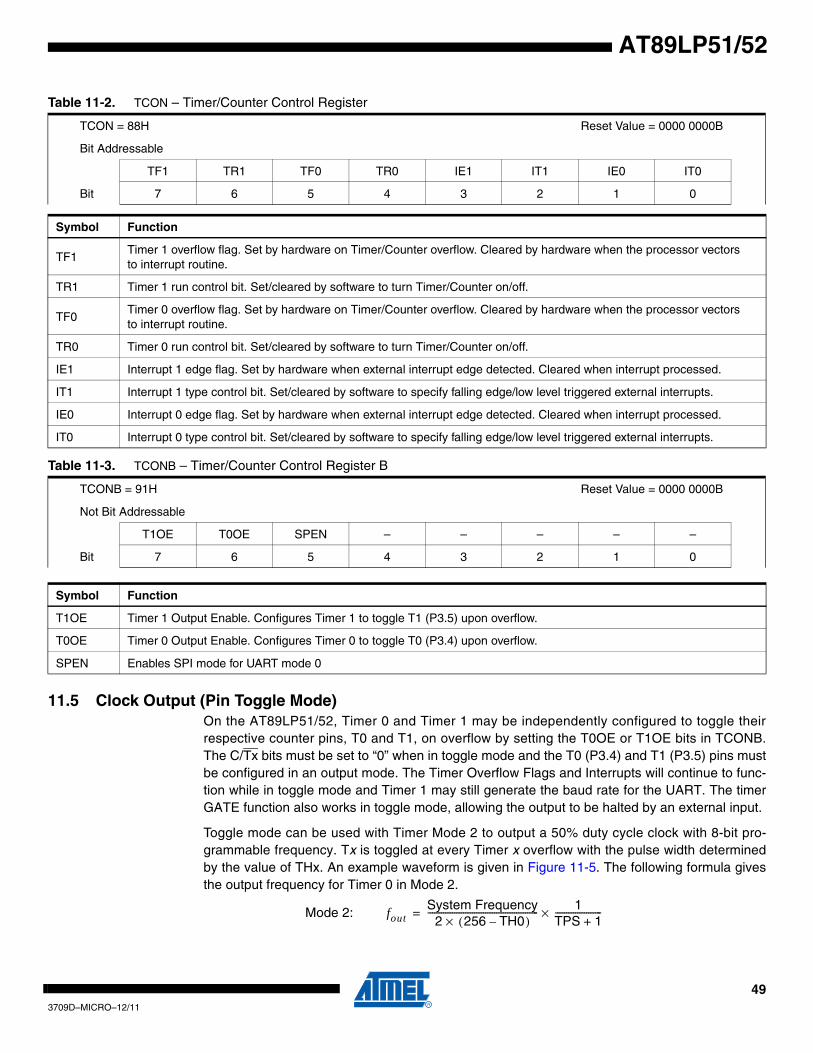
493709D–MICRO–12/11
AT89LP51/52
.
11.5 Clock Output (Pin Toggle Mode)On the AT89LP51/52, Timer 0 and Timer 1 may be independently configured to toggle theirrespective counter pins, T0 and T1, on overflow by setting the T0OE or T1OE bits in TCONB.The C/Tx bits must be set to “0” when in toggle mode and the T0 (P3.4) and T1 (P3.5) pins mustbe configured in an output mode. The Timer Overflow Flags and Interrupts will continue to func-tion while in toggle mode and Timer 1 may still generate the baud rate for the UART. The timerGATE function also works in toggle mode, allowing the output to be halted by an external input.
Toggle mode can be used with Timer Mode 2 to output a 50% duty cycle clock with 8-bit pro-grammable frequency. Tx is toggled at every Timer x overflow with the pulse width determinedby the value of THx. An example waveform is given in Figure 11-5. The following formula givesthe output frequency for Timer 0 in Mode 2.
Table 11-2. TCON – Timer/Counter Control Register
TCON = 88H Reset Value = 0000 0000B
Bit Addressable
TF1 TR1 TF0 TR0 IE1 IT1 IE0 IT0
Bit 7 6 5 4 3 2 1 0
Symbol Function
TF1Timer 1 overflow flag. Set by hardware on Timer/Counter overflow. Cleared by hardware when the processor vectors to interrupt routine.
TR1 Timer 1 run control bit. Set/cleared by software to turn Timer/Counter on/off.
TF0Timer 0 overflow flag. Set by hardware on Timer/Counter overflow. Cleared by hardware when the processor vectors to interrupt routine.
TR0 Timer 0 run control bit. Set/cleared by software to turn Timer/Counter on/off.
IE1 Interrupt 1 edge flag. Set by hardware when external interrupt edge detected. Cleared when interrupt processed.
IT1 Interrupt 1 type control bit. Set/cleared by software to specify falling edge/low level triggered external interrupts.
IE0 Interrupt 0 edge flag. Set by hardware when external interrupt edge detected. Cleared when interrupt processed.
IT0 Interrupt 0 type control bit. Set/cleared by software to specify falling edge/low level triggered external interrupts.
Table 11-3. TCONB – Timer/Counter Control Register B
TCONB = 91H Reset Value = 0000 0000B
Not Bit Addressable
T1OE T0OE SPEN – – – – –
Bit 7 6 5 4 3 2 1 0
Symbol Function
T1OE Timer 1 Output Enable. Configures Timer 1 to toggle T1 (P3.5) upon overflow.
T0OE Timer 0 Output Enable. Configures Timer 0 to toggle T0 (P3.4) upon overflow.
SPEN Enables SPI mode for UART mode 0
Mode 2: foutSystem Frequency
2 256 TH0–( )×-------------------------------------------------- 1
TPS 1+---------------------×=
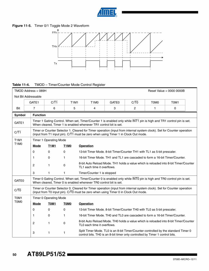
503709D–MICRO–12/11
AT89LP51/52
Figure 11-5. Timer 0/1 Toggle Mode 2 Waveform
Tx
THx
FFh
Table 11-4. TMOD – Timer/Counter Mode Control Register
TMOD Address = 089H Reset Value = 0000 0000B
Not Bit Addressable
GATE1 C/T1 T1M1 T1M0 GATE0 C/T0 T0M0 T0M1
Bit 7 6 5 4 3 2 1 0
Symbol Function
GATE1Timer 1 Gating Control. When set, Timer/Counter 1 is enabled only while INT1 pin is high and TR1 control pin is set. When cleared, Timer 1 is enabled whenever TR1 control bit is set.
C/T1Timer or Counter Selector 1. Cleared for Timer operation (input from internal system clock). Set for Counter operation (input from T1 input pin). C/T1 must be zero when using Timer 1 in Clock Out mode.
T1M1T1M0
Timer 1 Operating Mode
Mode T1M1 T1M0 Operation
0 0 0 13-bit Timer Mode. 8-bit Timer/Counter TH1 with TL1 as 5-bit prescaler.
1 0 1 16-bit Timer Mode. TH1 and TL1 are cascaded to form a 16-bit Timer/Counter.
2 1 08-bit Auto Reload Mode. TH1 holds a value which is reloaded into 8-bit Timer/Counter TL1 each time it overflows.
3 1 1 Timer/Counter 1 is stopped
GATE0Timer 0 Gating Control. When set, Timer/Counter 0 is enabled only while INT0 pin is high and TR0 control pin is set. When cleared, Timer 0 is enabled whenever TR0 control bit is set.
C/T0Timer or Counter Selector 0. Cleared for Timer operation (input from internal system clock). Set for Counter operation (input from T0 input pin). C/T0 must be zero when using Timer 0 in Clock Out mode.
T0M1T0M0
Timer 0 Operating Mode
Mode T0M1 T0M0 Operation
0 0 0 13-bit Timer Mode. 8-bit Timer/Counter TH0 with TL0 as 5-bit prescaler.
1 0 1 16-bit Timer Mode. TH0 and TL0 are cascaded to form a 16-bit Timer/Counter.
2 1 08-bit Auto Reload Mode. TH0 holds a value which is reloaded into 8-bit Timer/Counter TL0 each time it overflows.
3 1 1Split Timer Mode. TL0 is an 8-bit Timer/Counter controlled by the standard Timer 0 control bits. TH0 is an 8-bit timer only controlled by Timer 1 control bits.
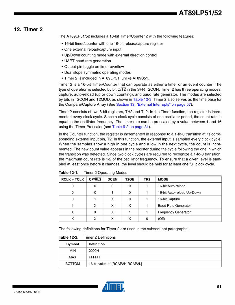
513709D–MICRO–12/11
AT89LP51/52
12. Timer 2The AT89LP51/52 includes a 16-bit Timer/Counter 2 with the following features:
• 16-bit timer/counter with one 16-bit reload/capture register
• One external reload/capture input
• Up/Down counting mode with external direction control
• UART baud rate generation
• Output-pin toggle on timer overflow
• Dual slope symmetric operating modes
• Timer 2 is included in AT89LP51, unlike AT89S51.
Timer 2 is a 16-bit Timer/Counter that can operate as either a timer or an event counter. Thetype of operation is selected by bit C/T2 in the SFR T2CON. Timer 2 has three operating modes:capture, auto-reload (up or down counting), and baud rate generator. The modes are selectedby bits in T2CON and T2MOD, as shown in Table 12-3. Timer 2 also serves as the time base forthe Compare/Capture Array (See Section 13. “External Interrupts” on page 57).
Timer 2 consists of two 8-bit registers, TH2 and TL2. In the Timer function, the register is incre-mented every clock cycle. Since a clock cycle consists of one oscillator period, the count rate isequal to the oscillator frequency. The timer rate can be prescaled by a value between 1 and 16using the Timer Prescaler (see Table 6-2 on page 31).
In the Counter function, the register is incremented in response to a 1-to-0 transition at its corre-sponding external input pin, T2. In this function, the external input is sampled every clock cycle.When the samples show a high in one cycle and a low in the next cycle, the count is incre-mented. The new count value appears in the register during the cycle following the one in whichthe transition was detected. Since two clock cycles are required to recognize a 1-to-0 transition,the maximum count rate is 1/2 of the oscillator frequency. To ensure that a given level is sam-pled at least once before it changes, the level should be held for at least one full clock cycle.
The following definitions for Timer 2 are used in the subsequent paragraphs:
Table 12-1. Timer 2 Operating Modes
RCLK + TCLK CP/RL2 DCEN T2OE TR2 MODE
0 0 0 0 1 16-bit Auto-reload
0 0 1 0 1 16-bit Auto-reload Up-Down
0 1 X 0 1 16-bit Capture
1 X X X 1 Baud Rate Generator
X X X 1 1 Frequency Generator
X X X X 0 (Off)
Table 12-2. Timer 2 Definitions
Symbol Definition
MIN 0000H
MAX FFFFH
BOTTOM 16-bit value of {RCAP2H,RCAP2L}
523709D–MICRO–12/11
AT89LP51/52
12.1 Timer 2 RegistersControl and status bits for Timer 2 are contained in registers T2CON (see Table 12-3) andT2MOD (see Table 12-4). The register pair {TH2, TL2} at addresses 0CDH and 0CCH are the16-bit timer register for Timer 2. The register pair {RCAP2H, RCAP2L} at addresses 0CBH and0CAH are the 16-bit Capture/Reload register for Timer 2 in capture and auto-reload modes.
Table 12-3. T2CON – Timer/Counter 2 Control Register
T2CON Address = 0C8H Reset Value = 0000 0000B
Bit Addressable
TF2 EXF2 RCLK TCLK EXEN2 TR2 C/T2 CP/RL2
Bit 7 6 5 4 3 2 1 0
Symbol Function
TF2Timer 2 overflow flag set by a Timer 2 overflow and must be cleared by software. TF2 will not be set when either RCLK = 1 or TCLK = 1.
EXF2Timer 2 external flag set when either a capture or reload is caused by a negative transition on T2EX and EXEN2 = 1. When Timer 2 interrupt is enabled, EXF2 = 1 will cause the CPU to vector to the Timer 2 interrupt routine. EXF2 must be cleared by software. EXF2 does not cause an interrupt in up/down counter mode (DCEN = 1) or dual-slope mode.
RCLKReceive clock enable. When set, causes the serial port to use Timer 2 overflow pulses for its receive clock in serial port Modes 1 and 3. RCLK = 0 causes Timer 1 overflows to be used for the receive clock.
TCLKTransmit clock enable. When set, causes the serial port to use Timer 2 overflow pulses for its transmit clock in serial port Modes 1 and 3. TCLK = 0 causes Timer 1 overflows to be used for the transmit clock.
EXEN2Timer 2 external enable. When set, allows a capture or reload to occur as a result of a negative transition on T2EX if Timer 2 is not being used to clock the serial port. EXEN2 = 0 causes Timer 2 to ignore events at T2EX.
TR2 Start/Stop control for Timer 2. TR2 = 1 starts the timer.
C/T2Timer or counter select for Timer 2. C/T2 = 0 for timer function. C/T2 = 1 for external event counter (falling edge triggered).
CP/RL2Capture/Reload select. CP/RL2 = 1 causes captures to occur on negative transitions at T2EX if EXEN2 = 1. CP/RL2 = 0 causes automatic reloads to occur when Timer 2 overflows or negative transitions occur at T2EX when EXEN2 = 1. When either RCLK or TCLK = 1, this bit is ignored and the timer is forced to auto-reload on Timer 2 overflow.
Table 12-4. T2MOD – Timer 2 Mode Control Register
T2MOD Address = 0C9H Reset Value = 0000 0000B
Not Bit Addressable
– – – – – – T2OE DCEN
Bit 7 6 5 4 3 2 1 0
Symbol Function
T2OE Timer 2 Output Enable. When T2OE = 1 and C/T2 = 0, the T2 pin will toggle after every Timer 2 overflow.
DCEN Timer 2 Down Count Enable. When Timer 2 operates in Auto-Reload mode and EXEN2 = 1, setting DCEN = 1 will cause Timer 2 to count up or down depending on the state of T2EX.
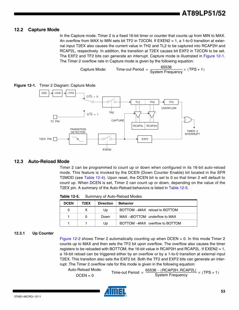
533709D–MICRO–12/11
AT89LP51/52
12.2 Capture ModeIn the Capture mode, Timer 2 is a fixed 16-bit timer or counter that counts up from MIN to MAX.An overflow from MAX to MIN sets bit TF2 in T2CON. If EXEN2 = 1, a 1-to-0 transition at exter-nal input T2EX also causes the current value in TH2 and TL2 to be captured into RCAP2H andRCAP2L, respectively. In addition, the transition at T2EX causes bit EXF2 in T2CON to be set.The EXF2 and TF2 bits can generate an interrupt. Capture mode is illustrated in Figure 12-1.The Timer 2 overflow rate in Capture mode is given by the following equation:
Figure 12-1. Timer 2 Diagram: Capture Mode
12.3 Auto-Reload ModeTimer 2 can be programmed to count up or down when configured in its 16-bit auto-reloadmode. This feature is invoked by the DCEN (Down Counter Enable) bit located in the SFRT2MOD (see Table 12-4). Upon reset, the DCEN bit is set to 0 so that timer 2 will default tocount up. When DCEN is set, Timer 2 can count up or down, depending on the value of theT2EX pin. A summary of the Auto-Reload behaviors is listed in Table 12-5.
12.3.1 Up CounterFigure 12-2 shows Timer 2 automatically counting up when DCEN = 0. In this mode Timer 2counts up to MAX and then sets the TF2 bit upon overflow. The overflow also causes the timerregisters to be reloaded with BOTTOM, the 16-bit value in RCAP2H and RCAP2L. If EXEN2 = 1,a 16-bit reload can be triggered either by an overflow or by a 1-to-0 transition at external inputT2EX. This transition also sets the EXF2 bit. Both the TF2 and EXF2 bits can generate an inter-rupt. The Timer 2 overflow rate for this mode is given in the following equation:
Capture Mode: Time-out Period65536
System Frequency-------------------------------------------------- TPS 1+( )×=
÷TPS
EXF2 T2EX PI N
T2 PI N
TR2
EXEN2
C/T2 = 0
C/T2 = 1
CAPTURE
O VERFLO W
TRANSITION DETECT OR TIMER 2
INTERR UPT
RCAP2H RCAP2L
TL2 TH2 TF2
OSC ÷CDV
Table 12-5. Summary of Auto-Reload Modes
DCEN T2EX Direction Behavior
0 X Up reload to BOTTOM
1 0 Down underflow to MAX
1 1 Up overflow to BOTTOM
BOTTOM MAX→
MAX BOTTOM→
BOTTOM MAX→
Auto-Reload Mode:
DCEN = 0Time-out Period
65536 RCAP2H RCAP2L{ , }–System Frequency
------------------------------------------------------------------------------- TPS 1+( )×=
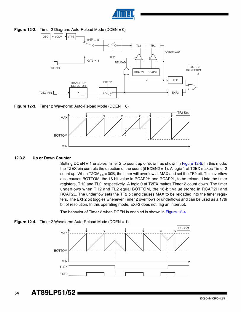
543709D–MICRO–12/11
AT89LP51/52
Figure 12-2. Timer 2 Diagram: Auto-Reload Mode (DCEN = 0)
Figure 12-3. Timer 2 Waveform: Auto-Reload Mode (DCEN = 0)
12.3.2 Up or Down CounterSetting DCEN = 1 enables Timer 2 to count up or down, as shown in Figure 12-5. In this mode,the T2EX pin controls the direction of the count (if EXEN2 = 1). A logic 1 at T2EX makes Timer 2count up. When T2CM1-0 = 00B, the timer will overflow at MAX and set the TF2 bit. This overflowalso causes BOTTOM, the 16-bit value in RCAP2H and RCAP2L, to be reloaded into the timerregisters, TH2 and TL2, respectively. A logic 0 at T2EX makes Timer 2 count down. The timerunderflows when TH2 and TL2 equal BOTTOM, the 16-bit value stored in RCAP2H andRCAP2L. The underflow sets the TF2 bit and causes MAX to be reloaded into the timer regis-ters. The EXF2 bit toggles whenever Timer 2 overflows or underflows and can be used as a 17thbit of resolution. In this operating mode, EXF2 does not flag an interrupt.
The behavior of Timer 2 when DCEN is enabled is shown in Figure 12-4.
Figure 12-4. Timer 2 Waveform: Auto-Reload Mode (DCEN = 1)
÷CDV
TL2 TH2
OSC ÷TPS
MAX
MIN
BOTTOM
TF2 Set
MAX
MIN
BOTTOM
T2EX
TF2 Set
EXF2
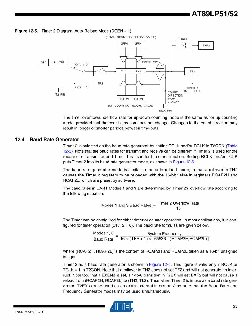
553709D–MICRO–12/11
AT89LP51/52
Figure 12-5. Timer 2 Diagram: Auto-Reload Mode (DCEN = 1)
The timer overflow/underflow rate for up-down counting mode is the same as for up countingmode, provided that the count direction does not change. Changes to the count direction mayresult in longer or shorter periods between time-outs.
12.4 Baud Rate GeneratorTimer 2 is selected as the baud rate generator by setting TCLK and/or RCLK in T2CON (Table12-3). Note that the baud rates for transmit and receive can be different if Timer 2 is used for thereceiver or transmitter and Timer 1 is used for the other function. Setting RCLK and/or TCLKputs Timer 2 into its baud rate generator mode, as shown in Figure 12-6.
The baud rate generator mode is similar to the auto-reload mode, in that a rollover in TH2causes the Timer 2 registers to be reloaded with the 16-bit value in registers RCAP2H andRCAP2L, which are preset by software.
The baud rates in UART Modes 1 and 3 are determined by Timer 2’s overflow rate according tothe following equation.
The Timer can be configured for either timer or counter operation. In most applications, it is con-figured for timer operation (CP/T2 = 0). The baud rate formulas are given below.
where (RCAP2H, RCAP2L) is the content of RCAP2H and RCAP2L taken as a 16-bit unsignedinteger.
Timer 2 as a baud rate generator is shown in Figure 12-6. This figure is valid only if RCLK orTCLK = 1 in T2CON. Note that a rollover in TH2 does not set TF2 and will not generate an inter-rupt. Note too, that if EXEN2 is set, a 1-to-0 transition in T2EX will set EXF2 but will not cause areload from (RCAP2H, RCAP2L) to (TH2, TL2). Thus when Timer 2 is in use as a baud rate gen-erator, T2EX can be used as an extra external interrupt. Also note that the Baud Rate andFrequency Generator modes may be used simultaneously.
÷TPS
Modes 1 and 3 Baud Rates Timer 2 Overflow Rate16
------------------------------------------------------------=
Modes 1, 3
Baud RateSystem Frequency
16 TPS 1+( )× 65536 RCAP2H,RCAP2L( )–[ ]×---------------------------------------------------------------------------------------------------------------------------------=
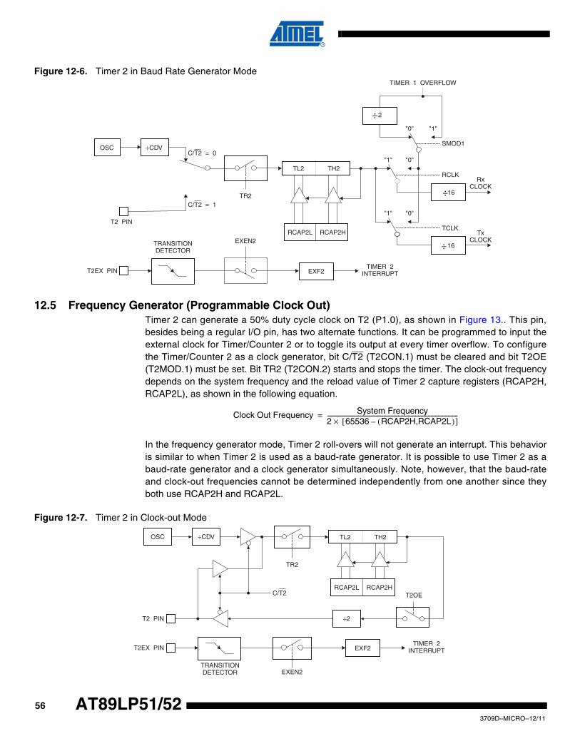
563709D–MICRO–12/11
AT89LP51/52
Figure 12-6. Timer 2 in Baud Rate Generator Mode
12.5 Frequency Generator (Programmable Clock Out)Timer 2 can generate a 50% duty cycle clock on T2 (P1.0), as shown in Figure 13.. This pin,besides being a regular I/O pin, has two alternate functions. It can be programmed to input theexternal clock for Timer/Counter 2 or to toggle its output at every timer overflow. To configurethe Timer/Counter 2 as a clock generator, bit C/T2 (T2CON.1) must be cleared and bit T2OE(T2MOD.1) must be set. Bit TR2 (T2CON.2) starts and stops the timer. The clock-out frequencydepends on the system frequency and the reload value of Timer 2 capture registers (RCAP2H,RCAP2L), as shown in the following equation.
In the frequency generator mode, Timer 2 roll-overs will not generate an interrupt. This behavioris similar to when Timer 2 is used as a baud-rate generator. It is possible to use Timer 2 as abaud-rate generator and a clock generator simultaneously. Note, however, that the baud-rateand clock-out frequencies cannot be determined independently from one another since theyboth use RCAP2H and RCAP2L.
Figure 12-7. Timer 2 in Clock-out Mode
÷CDVSMOD1
RCLK
TCLK
Rx CLOCK
Tx CLOCK
T2EX PI N
T2 PI N
TR2
"1"
"1"
"1"
"0"
"0"
"0"
TIMER 1 OVERFLOW
TIMER 2 INTERR UPT
2
16
16
RCAP2H RCAP2L
TL2 TH2
C/T2 = 0
C/T2 = 1
EXF2
TRANSITION DETECT OR
EXEN2
÷
÷
÷
OSC
Clock Out Frequency System Frequency2 65536 RCAP2H,RCAP2L( )–[ ]×--------------------------------------------------------------------------------------------=
OSC
T2EX PIN
T2 PIN
TR2
TIMER 2INTERRUPT
RCAP2HRCAP2L
TL2 TH2
C/T2
EXF2
TRANSITIONDETECTOR EXEN2
÷CDV
÷2
T2OE
573709D–MICRO–12/11
AT89LP51/52
13. External InterruptsThe INT0 (P3.2) and INT1 (P3.3) pins of the AT89LP51/52 may be used as external interruptsources. The external interrupts can be programmed to be level-activated or transition-activatedby setting or clearing bit IT1 or IT0 in Register TCON. If ITx = 0, external interrupt x is triggeredby a detected low at the INTx pin. If ITx = 1, external interrupt x is edge-triggered. In this mode ifsuccessive samples of the INTx pin show a high in one cycle and a low in the next cycle, inter-rupt request flag IEx in TCON is set. Flag bit IEx then requests the interrupt. Since the externalinterrupt pins are sampled once each clock cycle, an input high or low should hold for at least 2system periods to ensure sampling. If the external interrupt is transition-activated, the externalsource has to hold the request pin high for at least two clock cycles, and then hold it low for atleast two clock cycles to ensure that the transition is seen so that interrupt request flag IEx willbe set. IEx will be automatically cleared by the CPU when the service routine is called if gener-ated in edge-triggered mode. If the external interrupt is level-activated, the external source hasto hold the request active until the requested interrupt is actually generated. Then the externalsource must deactivate the request before the interrupt service routine is completed, or elseanother interrupt will be generated. Both INT0 and INT1 may wake up the device from thePower-down state.
14. Serial Interface (UART)The seria l interface on the AT89LP51/52 implements a Universa l AsynchronousReceiver/Transmitter (UART). The UART has the following features:
• Full-duplex Operation
• 8 or 9 Data Bits
• Framing Error Detection
• Multiprocessor Communication Mode with Automatic Address Recognition
• Baud Rate Generator Using Timer 1 or Timer 2
• Interrupt on Receive Buffer Full or Transmission Complete
• Synchronous SPI or TWI Master Emulation
The serial interface is full-duplex, which means it can transmit and receive simultaneously. It isalso receive-buffered, which means it can begin receiving a second byte before a previouslyreceived byte has been read from the receive register. (However, if the first byte still has notbeen read when reception of the second byte is complete, one of the bytes will be lost.) Theserial port receive and transmit registers are both accessed at the Special Function RegisterSBUF. Writing to SBUF loads the transmit register, and reading SBUF accesses a physicallyseparate receive register. The serial port can operate in the following four modes.
• Mode 0: Serial data enters and exits through RXD. TXD outputs the shift clock. Eight data bits are transmitted/received, with the LSB first. The baud rate is programmable to 1/6 or 1/3 the system frequency in Compatibility mode, 1/4 or 1/2 the system frequency in Fast mode, or variable based on Time 1.
• Mode 1: 10 bits are transmitted (through TXD) or received (through RXD): a start bit (0), 8 data bits (LSB first), and a stop bit (1). On receive, the stop bit goes into RB8 in the Special Function Register SCON. The baud rate is variable based on Timer 1 or Timer 2.
• Mode 2: 11 bits are transmitted (through TXD) or received (through RXD): a start bit (0), 8 data bits (LSB first), a programmable 9th data bit, and a stop bit (1). On transmit, the 9th data bit (TB8 in SCON) can be assigned the value of “0” or “1”. For example, the parity bit (P, in the PSW) can be moved into TB8. On receive, the 9th data bit goes into RB8 in the
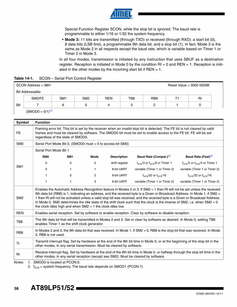
583709D–MICRO–12/11
AT89LP51/52
Special Function Register SCON, while the stop bit is ignored. The baud rate is programmable to either 1/16 or 1/32 the system frequency.
• Mode 3: 11 bits are transmitted (through TXD) or received (through RXD): a start bit (0), 8 data bits (LSB first), a programmable 9th data bit, and a stop bit (1). In fact, Mode 3 is the same as Mode 2 in all respects except the baud rate, which is variable based on Timer 1 or Timer 2 in Mode 3.
In all four modes, transmission is initiated by any instruction that uses SBUF as a destinationregister. Reception is initiated in Mode 0 by the condition RI = 0 and REN = 1. Reception is initi-ated in the other modes by the incoming start bit if REN = 1.
Notes: 1. SMOD0 is located at PCON.6.2. fSYS = system frequency. The baud rate depends on SMOD1 (PCON.7).
Table 14-1. SCON – Serial Port Control Register
SCON Address = 98H Reset Value = 0000 0000B
Bit Addressable
SM0/FE SM1 SM2 REN TB8 RB8 T1 RI
Bit 7 6 5 4 3 2 1 0
(SMOD0 = 0/1)(1)
Symbol Function
FEFraming error bit. This bit is set by the receiver when an invalid stop bit is detected. The FE bit is not cleared by valid frames and must be cleared by software. The SMOD0 bit must be set to enable access to the FE bit. FE will be set regardless of the state of SMOD0.
SM0 Serial Port Mode Bit 0, (SMOD0 must = 0 to access bit SM0)
SM1
Serial Port Mode Bit 1
SM2
Enables the Automatic Address Recognition feature in Modes 2 or 3. If SM2 = 1 then Rl will not be set unless the received 9th data bit (RB8) is 1, indicating an address, and the received byte is a Given or Broadcast Address. In Mode 1, if SM2 = 1 then Rl will not be activated unless a valid stop bit was received, and the received byte is a Given or Broadcast Address. In Mode 0, SM2 determines the idle state of the shift clock such that the clock is the inverse of SM2, i.e. when SM2 = 0 the clock idles high and when SM2 = 1 the clock idles low.
REN Enables serial reception. Set by software to enable reception. Clear by software to disable reception.
TB8The 9th data bit that will be transmitted in Modes 2 and 3. Set or clear by software as desired. In Mode 0, setting TB8 enables Timer 1 as the shift clock generator.
RB8In Modes 2 and 3, the 9th data bit that was received. In Mode 1, if SM2 = 0, RB8 is the stop bit that was received. In Mode 0, RB8 is not used.
TITransmit interrupt flag. Set by hardware at the end of the 8th bit time in Mode 0, or at the beginning of the stop bit in the other modes, in any serial transmission. Must be cleared by software.
RIReceive interrupt flag. Set by hardware at the end of the 8th bit time in Mode 0, or halfway through the stop bit time in the other modes, in any serial reception (except see SM2). Must be cleared by software.
SM0 SM1 Mode Description Baud Rate (Compat.)(2) Baud Rate (Fast)(2)
0 0 0 shift register fSYS/3 or fSYS/6 or Timer 1 fSYS/2 or fSYS/4 or Timer 1
0 1 1 8-bit UART variable (Timer 1 or Timer 2) variable (Timer 1 or Timer 2)
1 0 2 9-bit UART fSYS/32 or fSYS/16 fSYS/32 or fSYS/16
1 1 3 9-bit UART variable (Timer 1 or Timer 2) variable (Timer 1 or Timer 2)
593709D–MICRO–12/11
AT89LP51/52
14.1 Multiprocessor CommunicationsModes 2 and 3 have a special provision for multiprocessor communications. In these modes,9 data bits are received, followed by a stop bit. The 9th bit goes into RB8. Then comes a stop bit.The port can be programmed such that when the stop bit is received, the serial port interrupt isactivated only if RB8 = 1. This feature is enabled by setting bit SM2 in SCON.
The following example shows how to use the serial interrupt for multiprocessor communications.When the master processor must transmit a block of data to one of several slaves, it first sendsout an address byte that identifies the target slave. An address byte differs from a data byte inthat the 9th bit is “1” in an address byte and “0” in a data byte. With SM2 = 1, no slave isinterrupted by a data byte. An address byte, however, interrupts all slaves. Each slave canexamine the received byte and see if it is being addressed. The addressed slave clears its SM2bit and prepares to receive the data bytes that follows. The slaves that are not addressed settheir SM2 bits and ignore the data bytes. See “Automatic Address Recognition” on page 61.
The SM2 bit can be used to check the validity of the stop bit in Mode 1. In a Mode 1 reception, ifSM2 = 1, the receive interrupt is not activated unless a valid stop bit is received.
14.2 Baud RatesThe baud rate in Mode 0 depends on the value of the SMOD1 bit in Special Function RegisterPCON.7. If SMOD1 = 0 (the value on reset) and TB8 = 0, the baud rate is 1/4 of the system fre-quency in Fast mode. If SMOD1 = 1 and TB8 = 0, the baud rate is 1/2 of the system frequency,as shown in the following equation:
:In Compatibility mode the baud rate is 1/6 of the system frequency, scaling to 1/3 whenSMOD1 = 1.
The baud rate in Mode 2 also depends on the value of the SMOD1 bit. If SMOD1 = 0, the baudrate is 1/32 of the system frequency. If SMOD1 = 1, the baud rate is 1/16 of the system fre-quency, as shown in the following equation:
14.2.1 Using Timer 1 to Generate Baud RatesSetting TB8 = 1 in Mode 0 enables Timer 1 as the baud rate generator. When Timer 1 is thebaud rate generator for Mode 0, the baud rates are determined by the Timer 1 overflow rate andthe value of SMOD1 according to the following equation:
Mode 0 Baud Rate
TB8 = 0
2SMOD1
4-------------------- System Frequency×=
Mode 0 Baud Rate
TB8 = 0
2SMOD1
6-------------------- System Frequency×=
Mode 2 Baud Rate2
SMOD1
32-------------------- System Frequency×=
Mode 0 Baud Rate
TB8 = 1
2SMOD1
4-------------------- (Timer 1 Overflow Rate)×=
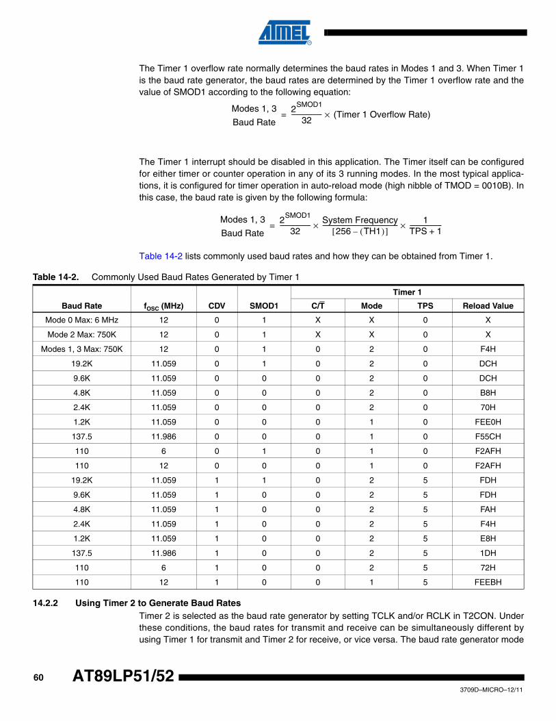
603709D–MICRO–12/11
AT89LP51/52
The Timer 1 overflow rate normally determines the baud rates in Modes 1 and 3. When Timer 1is the baud rate generator, the baud rates are determined by the Timer 1 overflow rate and thevalue of SMOD1 according to the following equation:
The Timer 1 interrupt should be disabled in this application. The Timer itself can be configuredfor either timer or counter operation in any of its 3 running modes. In the most typical applica-tions, it is configured for timer operation in auto-reload mode (high nibble of TMOD = 0010B). Inthis case, the baud rate is given by the following formula:
Table 14-2 lists commonly used baud rates and how they can be obtained from Timer 1.
14.2.2 Using Timer 2 to Generate Baud RatesTimer 2 is selected as the baud rate generator by setting TCLK and/or RCLK in T2CON. Underthese conditions, the baud rates for transmit and receive can be simultaneously different byusing Timer 1 for transmit and Timer 2 for receive, or vice versa. The baud rate generator mode
Modes 1, 3
Baud Rate
2SMOD1
32-------------------- (Timer 1 Overflow Rate)×=
Modes 1, 3
Baud Rate
2SMOD1
32-------------------- System Frequency
256 TH1( )–[ ]-------------------------------------------------- 1
TPS 1+---------------------××=
Table 14-2. Commonly Used Baud Rates Generated by Timer 1
Baud Rate fOSC (MHz) CDV SMOD1
Timer 1
C/T Mode TPS Reload Value
Mode 0 Max: 6 MHz 12 0 1 X X 0 X
Mode 2 Max: 750K 12 0 1 X X 0 X
Modes 1, 3 Max: 750K 12 0 1 0 2 0 F4H
19.2K 11.059 0 1 0 2 0 DCH
9.6K 11.059 0 0 0 2 0 DCH
4.8K 11.059 0 0 0 2 0 B8H
2.4K 11.059 0 0 0 2 0 70H
1.2K 11.059 0 0 0 1 0 FEE0H
137.5 11.986 0 0 0 1 0 F55CH
110 6 0 1 0 1 0 F2AFH
110 12 0 0 0 1 0 F2AFH
19.2K 11.059 1 1 0 2 5 FDH
9.6K 11.059 1 0 0 2 5 FDH
4.8K 11.059 1 0 0 2 5 FAH
2.4K 11.059 1 0 0 2 5 F4H
1.2K 11.059 1 0 0 2 5 E8H
137.5 11.986 1 0 0 2 5 1DH
110 6 1 0 0 2 5 72H
110 12 1 0 0 1 5 FEEBH
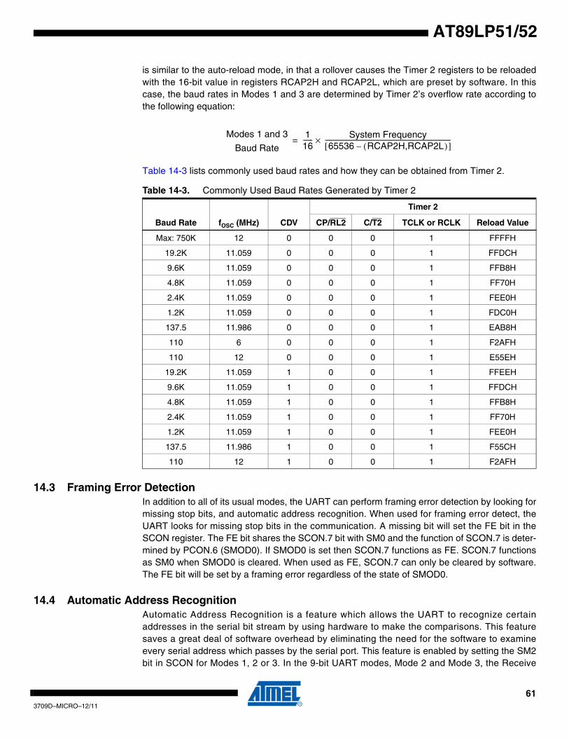
613709D–MICRO–12/11
AT89LP51/52
is similar to the auto-reload mode, in that a rollover causes the Timer 2 registers to be reloadedwith the 16-bit value in registers RCAP2H and RCAP2L, which are preset by software. In thiscase, the baud rates in Modes 1 and 3 are determined by Timer 2’s overflow rate according tothe following equation:
Table 14-3 lists commonly used baud rates and how they can be obtained from Timer 2.
14.3 Framing Error DetectionIn addition to all of its usual modes, the UART can perform framing error detection by looking formissing stop bits, and automatic address recognition. When used for framing error detect, theUART looks for missing stop bits in the communication. A missing bit will set the FE bit in theSCON register. The FE bit shares the SCON.7 bit with SM0 and the function of SCON.7 is deter-mined by PCON.6 (SMOD0). If SMOD0 is set then SCON.7 functions as FE. SCON.7 functionsas SM0 when SMOD0 is cleared. When used as FE, SCON.7 can only be cleared by software.The FE bit will be set by a framing error regardless of the state of SMOD0.
14.4 Automatic Address RecognitionAutomatic Address Recognition is a feature which allows the UART to recognize certainaddresses in the serial bit stream by using hardware to make the comparisons. This featuresaves a great deal of software overhead by eliminating the need for the software to examineevery serial address which passes by the serial port. This feature is enabled by setting the SM2bit in SCON for Modes 1, 2 or 3. In the 9-bit UART modes, Mode 2 and Mode 3, the Receive
Table 14-3. Commonly Used Baud Rates Generated by Timer 2
Baud Rate fOSC (MHz) CDV
Timer 2
CP/RL2 C/T2 TCLK or RCLK Reload Value
Max: 750K 12 0 0 0 1 FFFFH
19.2K 11.059 0 0 0 1 FFDCH
9.6K 11.059 0 0 0 1 FFB8H
4.8K 11.059 0 0 0 1 FF70H
2.4K 11.059 0 0 0 1 FEE0H
1.2K 11.059 0 0 0 1 FDC0H
137.5 11.986 0 0 0 1 EAB8H
110 6 0 0 0 1 F2AFH
110 12 0 0 0 1 E55EH
19.2K 11.059 1 0 0 1 FFEEH
9.6K 11.059 1 0 0 1 FFDCH
4.8K 11.059 1 0 0 1 FFB8H
2.4K 11.059 1 0 0 1 FF70H
1.2K 11.059 1 0 0 1 FEE0H
137.5 11.986 1 0 0 1 F55CH
110 12 1 0 0 1 F2AFH
Modes 1 and 3
Baud Rate
116------ System Frequency
65536 RCAP2H,RCAP2L( )–[ ]---------------------------------------------------------------------------------×=
623709D–MICRO–12/11
AT89LP51/52
Interrupt flag (RI) will be automatically set when the received byte contains either the “Given”address or the “Broadcast” address. The 9-bit mode requires that the 9th information bit be a “1”to indicate that the received information is an address and not data.
In Mode 1 (8-bit) the RI flag will be set if SM2 is enabled and the information received has a validstop bit following the 8th address bits and the information is either a Given or Broadcastaddress. Automatic Address Recognition is not available during Mode 0.
Using the Automatic Address Recognition feature allows a master to selectively communicatewith one or more slaves by invoking the given slave address or addresses. All of the slaves maybe contacted by using the Broadcast address. Two special Function Registers are used todefine the slave’s address, SADDR, and the address mask, SADEN. SADEN is used to definewhich bits in the SADDR are to be used and which bits are “don’t care”. The SADEN mask canbe logically ANDed with the SADDR to create the “Given” address which the master will use foraddressing each of the slaves. Use of the Given address allows multiple slaves to be recognizedwhile excluding others. The following examples show the versatility of this scheme:
Slave 0 SADDR = 1100 0000SADEN = 1111 1101Given = 1100 00X0
Slave 1 SADDR = 1100 0000SADEN = 1111 1110Given = 1100 000X
In the previous example, SADDR is the same and the SADEN data is used to differentiatebetween the two slaves. Slave 0 requires a “0” in bit 0 and it ignores bit 1. Slave 1 requires a “0”in bit 1 and bit 0 is ignored. A unique address for slave 0 would be 1100 0010 since slave 1requires a “0” in bit 1. A unique address for slave 1 would be 1100 0001 since a “1” in bit 0 willexclude slave 0. Both slaves can be selected at the same time by an address which has bit 0 = 0(for slave 0) and bit 1 = 0 (for slave 1). Thus, both could be addressed with 1100 0000.
In a more complex system, the following could be used to select slaves 1 and 2 while excludingslave 0:
Slave 0 SADDR = 1100 0000SADEN = 1111 1001Given = 1100 0XX0
Slave 1 SADDR = 1110 0000SADEN = 1111 1010Given = 1110 0X0X
Slave 2 SADDR = 1110 0000SADEN = 1111 1100Given = 1110 00XX
In the above example, the differentiation among the 3 slaves is in the lower 3 address bits. Slave0 requires that bit 0 = 0 and it can be uniquely addressed by 1110 0110. Slave 1 requires thatbit 1 = 0 and it can be uniquely addressed by 1110 and 0101. Slave 2 requires that bit 2 = 0 andits unique address is 1110 0011. To select Slaves 0 and 1 and exclude Slave 2, use address1110 0100, since it is necessary to make bit 2 = 1 to exclude slave 2.
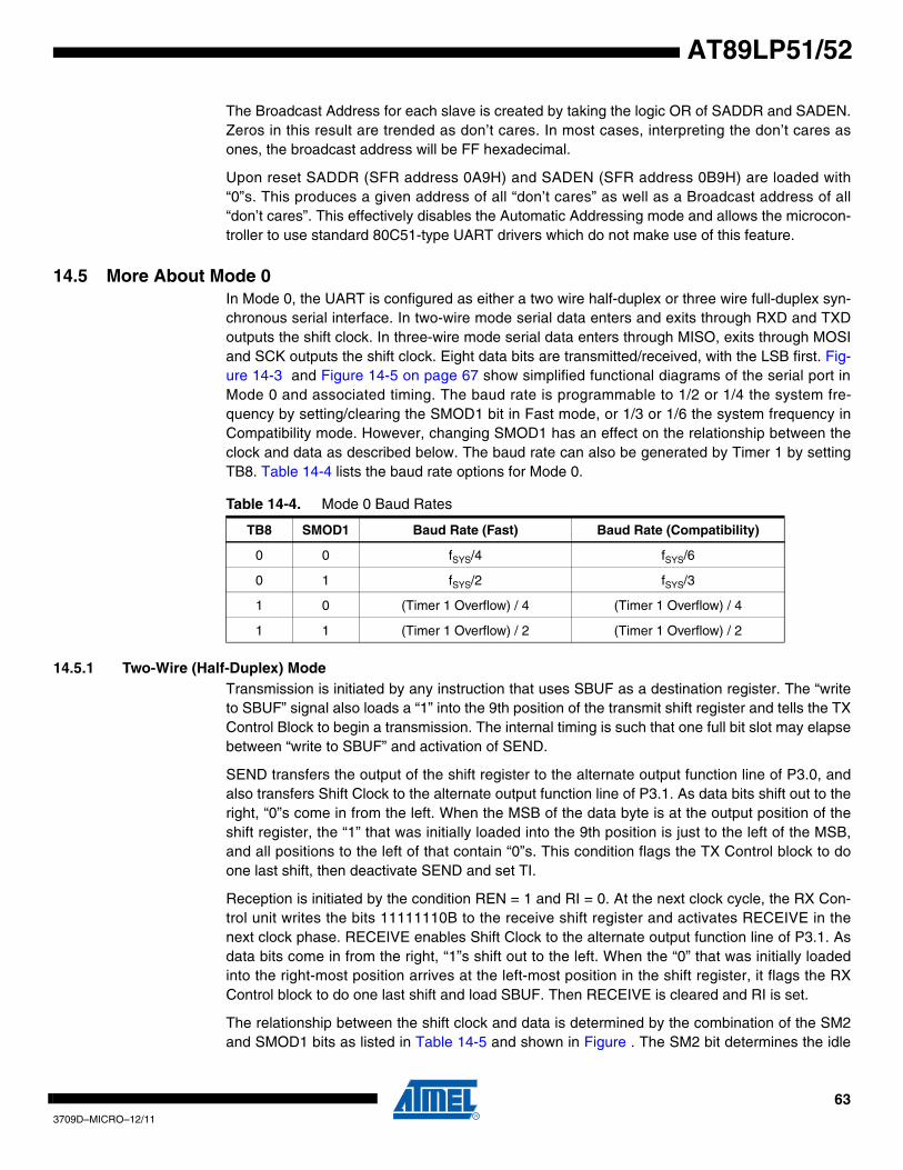
633709D–MICRO–12/11
AT89LP51/52
The Broadcast Address for each slave is created by taking the logic OR of SADDR and SADEN.Zeros in this result are trended as don’t cares. In most cases, interpreting the don’t cares asones, the broadcast address will be FF hexadecimal.
Upon reset SADDR (SFR address 0A9H) and SADEN (SFR address 0B9H) are loaded with“0”s. This produces a given address of all “don’t cares” as well as a Broadcast address of all“don’t cares”. This effectively disables the Automatic Addressing mode and allows the microcon-troller to use standard 80C51-type UART drivers which do not make use of this feature.
14.5 More About Mode 0In Mode 0, the UART is configured as either a two wire half-duplex or three wire full-duplex syn-chronous serial interface. In two-wire mode serial data enters and exits through RXD and TXDoutputs the shift clock. In three-wire mode serial data enters through MISO, exits through MOSIand SCK outputs the shift clock. Eight data bits are transmitted/received, with the LSB first. Fig-ure 14-3 and Figure 14-5 on page 67 show simplified functional diagrams of the serial port inMode 0 and associated timing. The baud rate is programmable to 1/2 or 1/4 the system fre-quency by setting/clearing the SMOD1 bit in Fast mode, or 1/3 or 1/6 the system frequency inCompatibility mode. However, changing SMOD1 has an effect on the relationship between theclock and data as described below. The baud rate can also be generated by Timer 1 by settingTB8. Table 14-4 lists the baud rate options for Mode 0.
14.5.1 Two-Wire (Half-Duplex) ModeTransmission is initiated by any instruction that uses SBUF as a destination register. The “writeto SBUF” signal also loads a “1” into the 9th position of the transmit shift register and tells the TXControl Block to begin a transmission. The internal timing is such that one full bit slot may elapsebetween “write to SBUF” and activation of SEND.
SEND transfers the output of the shift register to the alternate output function line of P3.0, andalso transfers Shift Clock to the alternate output function line of P3.1. As data bits shift out to theright, “0”s come in from the left. When the MSB of the data byte is at the output position of theshift register, the “1” that was initially loaded into the 9th position is just to the left of the MSB,and all positions to the left of that contain “0”s. This condition flags the TX Control block to doone last shift, then deactivate SEND and set TI.
Reception is initiated by the condition REN = 1 and RI = 0. At the next clock cycle, the RX Con-trol unit writes the bits 11111110B to the receive shift register and activates RECEIVE in thenext clock phase. RECEIVE enables Shift Clock to the alternate output function line of P3.1. Asdata bits come in from the right, “1”s shift out to the left. When the “0” that was initially loadedinto the right-most position arrives at the left-most position in the shift register, it flags the RXControl block to do one last shift and load SBUF. Then RECEIVE is cleared and RI is set.
The relationship between the shift clock and data is determined by the combination of the SM2and SMOD1 bits as listed in Table 14-5 and shown in Figure . The SM2 bit determines the idle
Table 14-4. Mode 0 Baud Rates
TB8 SMOD1 Baud Rate (Fast) Baud Rate (Compatibility)
0 0 fSYS/4 fSYS/6
0 1 fSYS/2 fSYS/3
1 0 (Timer 1 Overflow) / 4 (Timer 1 Overflow) / 4
1 1 (Timer 1 Overflow) / 2 (Timer 1 Overflow) / 2
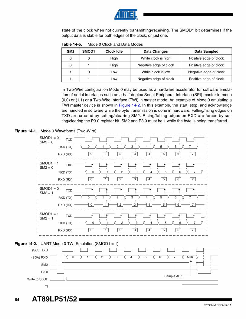
643709D–MICRO–12/11
AT89LP51/52
state of the clock when not currently transmitting/receiving. The SMOD1 bit determines if theoutput data is stable for both edges of the clock, or just one.
In Two-Wire configuration Mode 0 may be used as a hardware accelerator for software emula-tion of serial interfaces such as a half-duplex Serial Peripheral Interface (SPI) master in mode(0,0) or (1,1) or a Two-Wire Interface (TWI) in master mode. An example of Mode 0 emulating aTWI master device is shown in Figure 14-2. In this example, the start, stop, and acknowledgeare handled in software while the byte transmission is done in hardware. Falling/rising edges onTXD are created by setting/clearing SM2. Rising/falling edges on RXD are forced by set-ting/clearing the P3.0 register bit. SM2 and P3.0 must be 1 while the byte is being transferred.
Figure 14-1. Mode 0 Waveforms (Two-Wire)
Figure 14-2. UART Mode 0 TWI Emulation (SMOD1 = 1)
Table 14-5. Mode 0 Clock and Data Modes
SM2 SMOD1 Clock Idle Data Changes Data Sampled
0 0 High While clock is high Positive edge of clock
0 1 High Negative edge of clock Positive edge of clock
1 0 Low While clock is low Negative edge of clock
1 1 Low Negative edge of clock Positive edge of clock
7RXD (TX)
TXD
6543210
RXD (RX) 0 1 2 3 4 5 6 7
7RXD (TX)
TXD
6543210
RXD (RX) 0 1 2 3 4 5 6 7
7RXD (TX)
TXD
6543210
RXD (RX) 0 1 2 3 4 5 6 7
7RXD (TX)
TXD
6543210
RXD (RX) 0 1 2 3 4 5 6 7
SMOD1 = 0SM2 = 0
SMOD1 = 1SM2 = 0
SMOD1 = 0SM2 = 1
SMOD1 = 1SM2 = 1
7 (SDA) RXD
(SCL) TXD
6543210 ACK
SM2
P3.0
Write to SBUF
TI
Sample ACK
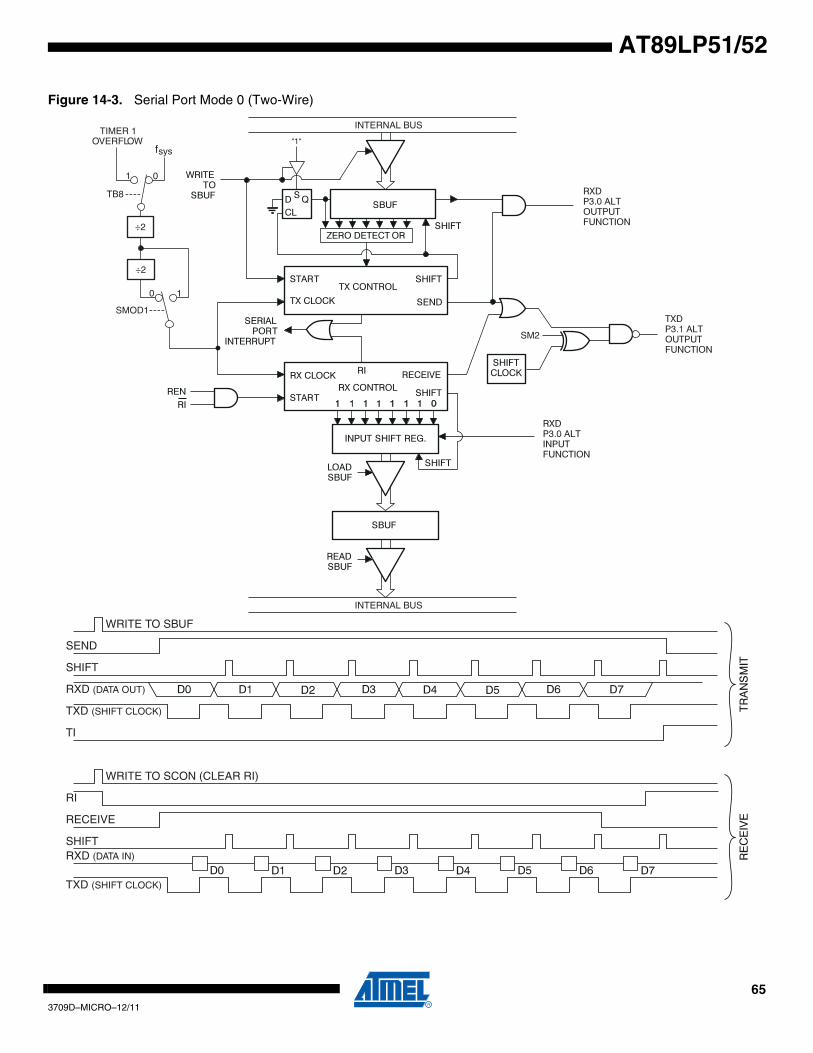
653709D–MICRO–12/11
AT89LP51/52
Figure 14-3. Serial Port Mode 0 (Two-Wire)
INTERNAL B U S
f sys
INTERNAL B U S
TXD (SHIFT CLOCK)
RXD ( D A T A OUT )
TXD (SHIFT CLOCK)
RXD ( D A T A IN )
WRITE T O S B U F
SEND
SHIFT
TI
WRITE T O SCON (CLEAR RI )
SHIFT
RECEIVE
RI
“1“
÷2
TB8
0 1
TIMER 1 O VERF L O W
÷2
SMOD1
0 1
SM2
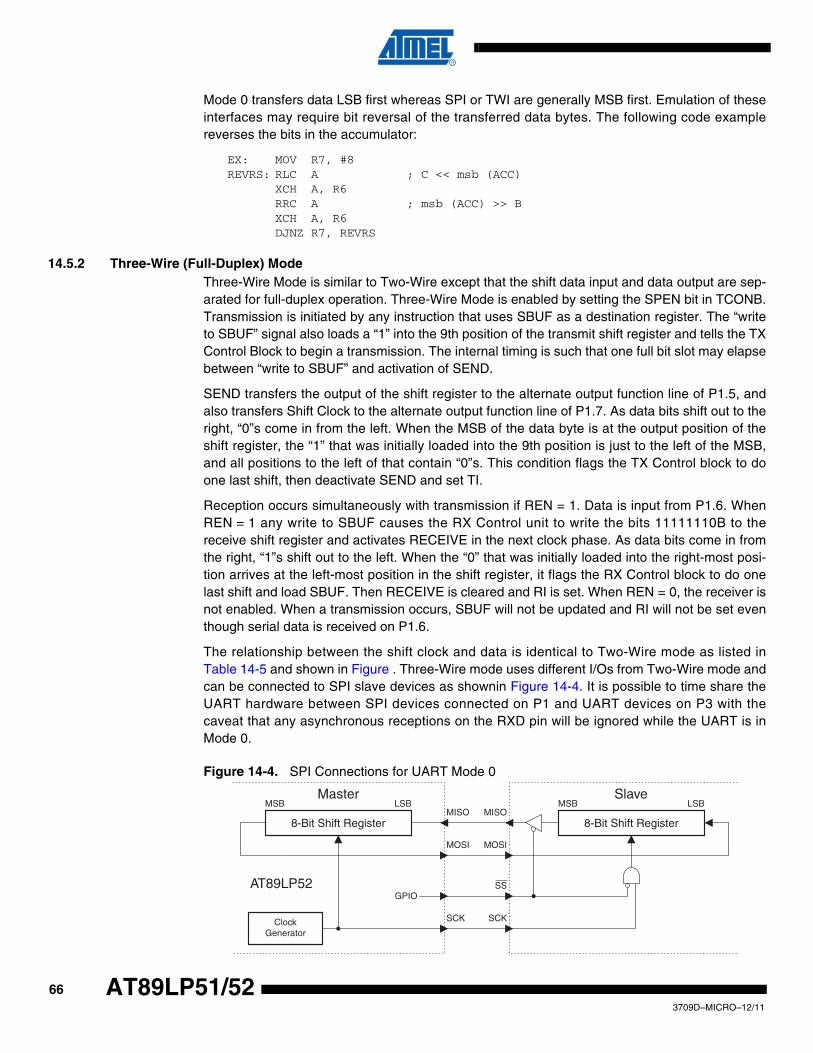
663709D–MICRO–12/11
AT89LP51/52
Mode 0 transfers data LSB first whereas SPI or TWI are generally MSB first. Emulation of theseinterfaces may require bit reversal of the transferred data bytes. The following code examplereverses the bits in the accumulator:
EX: MOV R7, #8REVRS: RLC A ; C << msb (ACC)
XCH A, R6RRC A ; msb (ACC) >> BXCH A, R6DJNZ R7, REVRS
14.5.2 Three-Wire (Full-Duplex) ModeThree-Wire Mode is similar to Two-Wire except that the shift data input and data output are sep-arated for full-duplex operation. Three-Wire Mode is enabled by setting the SPEN bit in TCONB.Transmission is initiated by any instruction that uses SBUF as a destination register. The “writeto SBUF” signal also loads a “1” into the 9th position of the transmit shift register and tells the TXControl Block to begin a transmission. The internal timing is such that one full bit slot may elapsebetween “write to SBUF” and activation of SEND.
SEND transfers the output of the shift register to the alternate output function line of P1.5, andalso transfers Shift Clock to the alternate output function line of P1.7. As data bits shift out to theright, “0”s come in from the left. When the MSB of the data byte is at the output position of theshift register, the “1” that was initially loaded into the 9th position is just to the left of the MSB,and all positions to the left of that contain “0”s. This condition flags the TX Control block to doone last shift, then deactivate SEND and set TI.
Reception occurs simultaneously with transmission if REN = 1. Data is input from P1.6. WhenREN = 1 any write to SBUF causes the RX Control unit to write the bits 11111110B to thereceive shift register and activates RECEIVE in the next clock phase. As data bits come in fromthe right, “1”s shift out to the left. When the “0” that was initially loaded into the right-most posi-tion arrives at the left-most position in the shift register, it flags the RX Control block to do onelast shift and load SBUF. Then RECEIVE is cleared and RI is set. When REN = 0, the receiver isnot enabled. When a transmission occurs, SBUF will not be updated and RI will not be set eventhough serial data is received on P1.6.
The relationship between the shift clock and data is identical to Two-Wire mode as listed inTable 14-5 and shown in Figure . Three-Wire mode uses different I/Os from Two-Wire mode andcan be connected to SPI slave devices as shownin Figure 14-4. It is possible to time share theUART hardware between SPI devices connected on P1 and UART devices on P3 with thecaveat that any asynchronous receptions on the RXD pin will be ignored while the UART is inMode 0.
Figure 14-4. SPI Connections for UART Mode 0
8-Bit Shift Register
Master Slave MSB LSB MSB LSB
8-Bit Shift Register MISO MISO
MOSI MOSI
SSGPIO
SCK SCKClockGenerator
AT89LP52
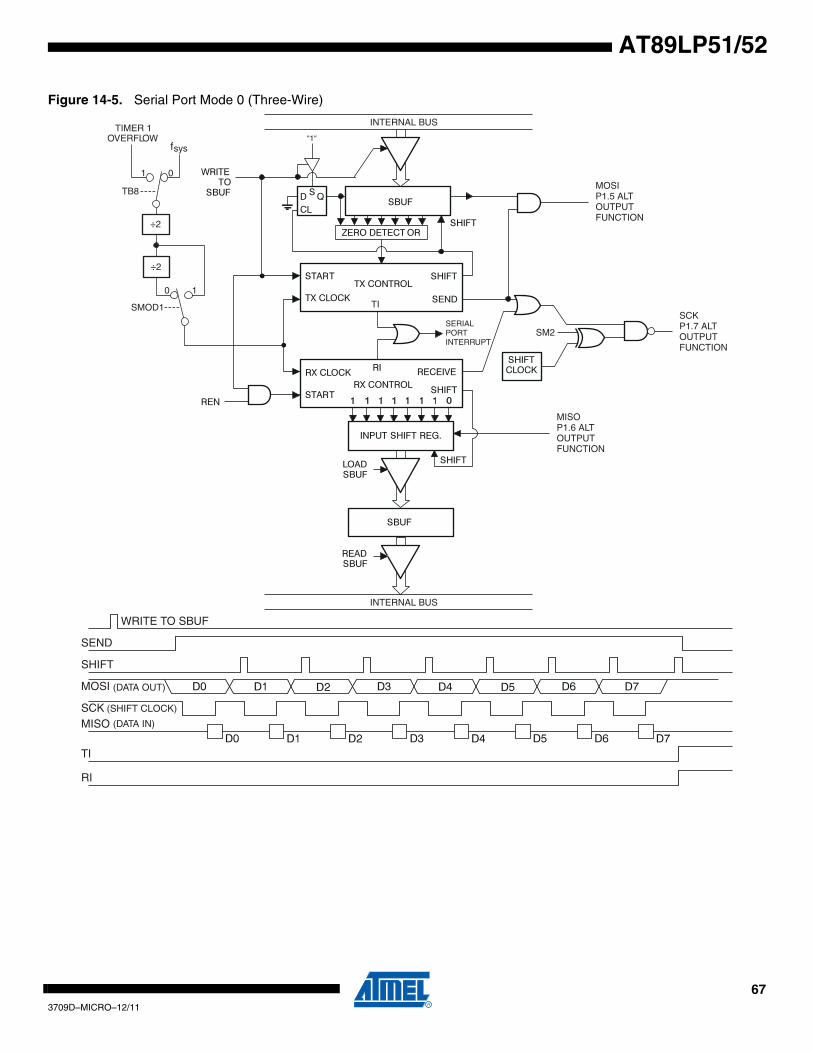
673709D–MICRO–12/11
AT89LP51/52
Figure 14-5. Serial Port Mode 0 (Three-Wire)
INTERNAL BUS
f sys
INTERNAL B U S
SCK (SHIFT CLOCK)
MOSI
MISO
WRITE T O S B U F
SEND
SHIFT
TI
“1“
÷2
TB8
0 1
TIMER 1O VERF L O W
÷2
SMOD1
0 1
SM2
MOSIP1.5 ALTOUTPUTFUNCTION
SCKP1.7 ALTOUTPUTFUNCTION
MISOP1.6 ALTOUTPUTFUNCTION
SERIALPORTINTERRUPT
TI
(DATA OUT)
(DATA IN)
RI
683709D–MICRO–12/11
AT89LP51/52
14.6 More About Mode 1Ten bits are transmitted (through TXD), or received (through RXD): a start bit (0), 8 data bits(LSB first), and a stop bit (1). On receive, the stop bit goes into RB8 in SCON. In theAT89LP51/52, the baud rate is determined either by the Timer 1 overflow rate, the TImer 2 over-flow rate, or both. In this case one timer is for transmit and the other is for receive. Figure 14-6shows a simplified functional diagram of the serial port in Mode 1 and associated timings fortransmit and receive.
Transmission is initiated by any instruction that uses SBUF as a destination register. The “writeto SBUF” signal also loads a “1” into the 9th bit position of the transmit shift register and flags theTX Control unit that a transmission is requested. Transmission actually commences at S1P1 ofthe machine cycle following the next rollover in the divide-by-16 counter. Thus, the bit times aresynchronized to the divide-by-16 counter, not to the “write to SBUF” signal.
The transmission begins when SEND is activated, which puts the start bit at TXD. One bit timelater, DATA is activated, which enables the output bit of the transmit shift register to TXD. Thefirst shift pulse occurs one bit time after that.
As data bits shift out to the right, “0”s are clocked in from the left. When the MSB of the data byteis at the output position of the shift register, the “1” that was initially loaded into the 9th position isjust to the left of the MSB, and all positions to the left of that contain “0”s. This condition flags theTX Control unit to do one last shift, then deactivate SEND and set TI. This occurs at the tenthdivide-by-16 rollover after “write to SBUF.”
Reception is initiated by a 1-to-0 transition detected at RXD. For this purpose, RXD is sampledat a rate of 16 times the established baud rate. When a transition is detected, the divide-by-16counter is immediately reset, and 1FFH is written into the input shift register. Resetting thedivide-by-16 counter aligns its roll-overs with the boundaries of the incoming bit times.
The 16 states of the counter divide each bit time into 16ths. At the 7th, 8th, and 9th counterstates of each bit time, the bit detector samples the value of RXD. The value accepted is thevalue that was seen in at least 2 of the 3 samples. This is done to reject noise. In order to rejectfalse bits, if the value accepted during the first bit time is not 0, the receive circuits are reset andthe unit continues looking for another 1-to-0 transition. If the start bit is valid, it is shifted into theinput shift register, and reception of the rest of the frame proceeds.
As data bits come in from the right, “1”s shift out to the left. When the start bit arrives at the left-most position in the shift register, (which is a 9-bit register in Mode 1), it flags the RX Controlblock to do one last shift, load SBUF and RB8, and set RI. The signal to load SBUF and RB8and to set RI is generated if, and only if, the following conditions are met at the time the final shiftpulse is generated.
RI = 0 and
Either SM2 = 0, or the received stop bit = 1
If either of these two conditions is not met, the received frame is irretrievably lost. If both condi-tions are met, the stop bit goes into RB8, the 8 data bits go into SBUF, and RI is activated. Atthis time, whether or not the above conditions are met, the unit continues looking for a 1-to-0transition in RXD.
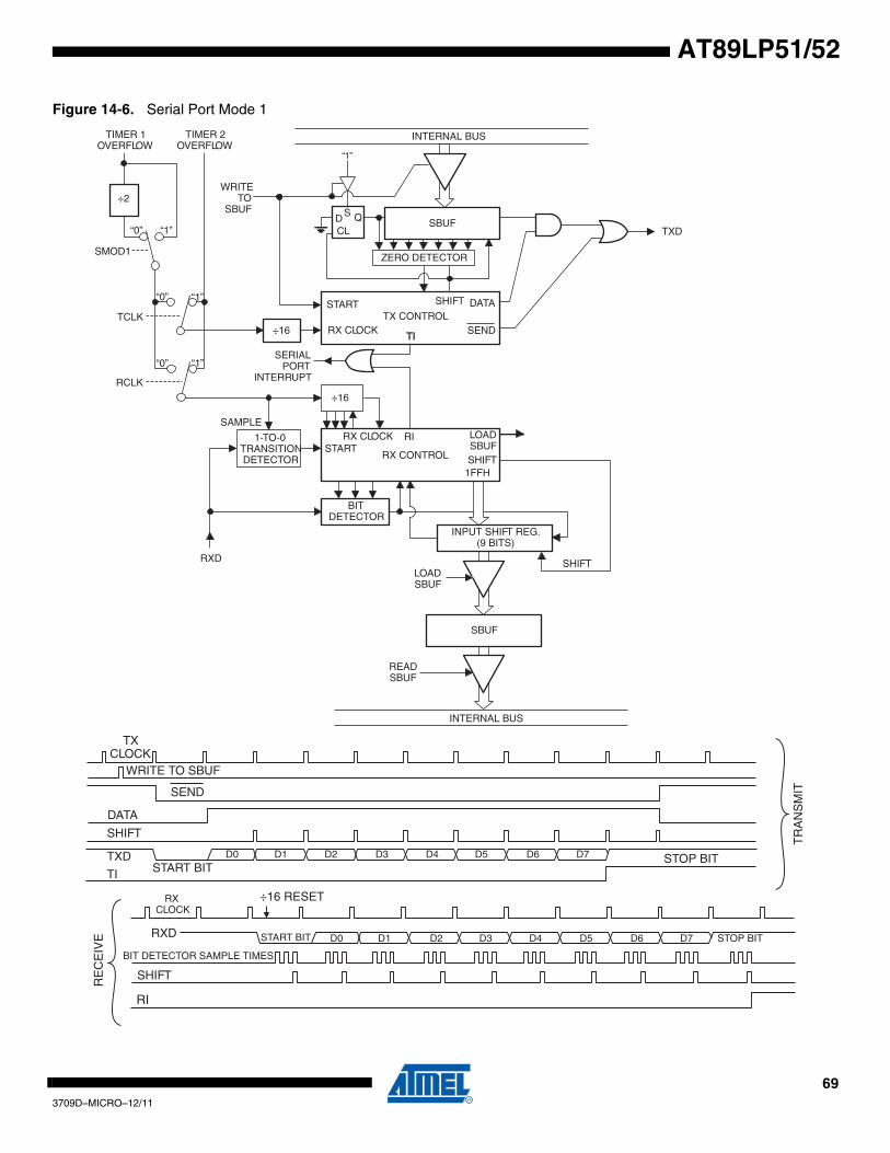
693709D–MICRO–12/11
AT89LP51/52
Figure 14-6. Serial Port Mode 1
TXCLOCK
WRITE TO SBUF
INTERNAL BUS
READSBUF
LOADSBUF
SBUF
SHIFT
INPUT SHIFT REG.(9 BITS)
BITDETECTOR
1-TO-0TRANSITIONDETECTOR
SERIALPORT
INTERRUPT
WRITETO
SBUF÷2
SMOD1
“0” “1”
TIMER 1OVERFLOW
RXD
RX CLOCK
RX CLOCK
RX CONTROLSTART
START DATA
SEND
SAMPLE
÷16
÷16TX CONTROL
TITI
ZERO DETECTOR
SBUFTXD
INTERNAL BUS
“1”
D QCL
S
LOADSBUFSHIFT
SHIFT
1FFH
RI
SEND
DATA
SHIFT
TXD
TI
D0 D1 D2 D3 D4 D5 D6 D7
D0 D1 D2 D3 D4 D5 D6 D7
STOP BIT
TR
AN
SM
IT
START BIT
÷16 RESET
START BIT STOP BIT
RXCLOCK
BIT DETECTOR SAMPLE TIMES
SHIFT
RE
CE
IVE RXD
RI
TIMER 2OVERFLOW
TCLK
RCLK
“0”
“0”
“1”
“1”
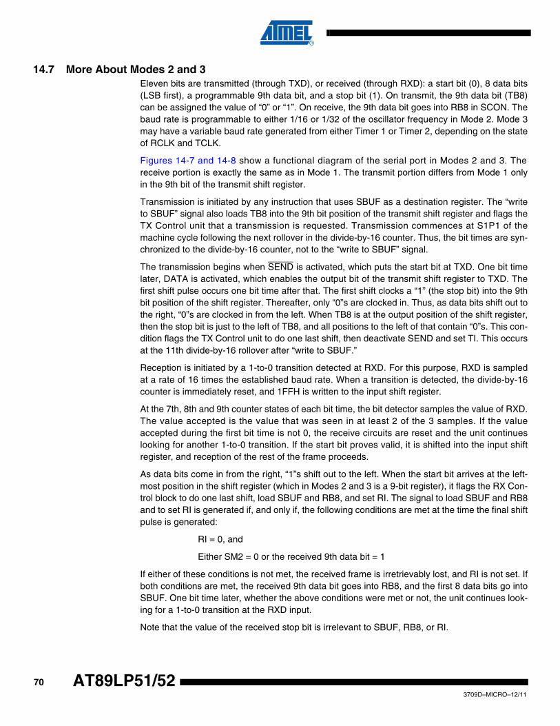
703709D–MICRO–12/11
AT89LP51/52
14.7 More About Modes 2 and 3Eleven bits are transmitted (through TXD), or received (through RXD): a start bit (0), 8 data bits(LSB first), a programmable 9th data bit, and a stop bit (1). On transmit, the 9th data bit (TB8)can be assigned the value of “0” or “1”. On receive, the 9th data bit goes into RB8 in SCON. Thebaud rate is programmable to either 1/16 or 1/32 of the oscillator frequency in Mode 2. Mode 3may have a variable baud rate generated from either Timer 1 or Timer 2, depending on the stateof RCLK and TCLK.
Figures 14-7 and 14-8 show a functional diagram of the serial port in Modes 2 and 3. Thereceive portion is exactly the same as in Mode 1. The transmit portion differs from Mode 1 onlyin the 9th bit of the transmit shift register.
Transmission is initiated by any instruction that uses SBUF as a destination register. The “writeto SBUF” signal also loads TB8 into the 9th bit position of the transmit shift register and flags theTX Control unit that a transmission is requested. Transmission commences at S1P1 of themachine cycle following the next rollover in the divide-by-16 counter. Thus, the bit times are syn-chronized to the divide-by-16 counter, not to the “write to SBUF” signal.
The transmission begins when SEND is activated, which puts the start bit at TXD. One bit timelater, DATA is activated, which enables the output bit of the transmit shift register to TXD. Thefirst shift pulse occurs one bit time after that. The first shift clocks a “1” (the stop bit) into the 9thbit position of the shift register. Thereafter, only “0”s are clocked in. Thus, as data bits shift out tothe right, “0”s are clocked in from the left. When TB8 is at the output position of the shift register,then the stop bit is just to the left of TB8, and all positions to the left of that contain “0”s. This con-dition flags the TX Control unit to do one last shift, then deactivate SEND and set TI. This occursat the 11th divide-by-16 rollover after “write to SBUF.”
Reception is initiated by a 1-to-0 transition detected at RXD. For this purpose, RXD is sampledat a rate of 16 times the established baud rate. When a transition is detected, the divide-by-16counter is immediately reset, and 1FFH is written to the input shift register.
At the 7th, 8th and 9th counter states of each bit time, the bit detector samples the value of RXD.The value accepted is the value that was seen in at least 2 of the 3 samples. If the valueaccepted during the first bit time is not 0, the receive circuits are reset and the unit continueslooking for another 1-to-0 transition. If the start bit proves valid, it is shifted into the input shiftregister, and reception of the rest of the frame proceeds.
As data bits come in from the right, “1”s shift out to the left. When the start bit arrives at the left-most position in the shift register (which in Modes 2 and 3 is a 9-bit register), it flags the RX Con-trol block to do one last shift, load SBUF and RB8, and set RI. The signal to load SBUF and RB8and to set RI is generated if, and only if, the following conditions are met at the time the final shiftpulse is generated:
RI = 0, and
Either SM2 = 0 or the received 9th data bit = 1
If either of these conditions is not met, the received frame is irretrievably lost, and RI is not set. Ifboth conditions are met, the received 9th data bit goes into RB8, and the first 8 data bits go intoSBUF. One bit time later, whether the above conditions were met or not, the unit continues look-ing for a 1-to-0 transition at the RXD input.
Note that the value of the received stop bit is irrelevant to SBUF, RB8, or RI.
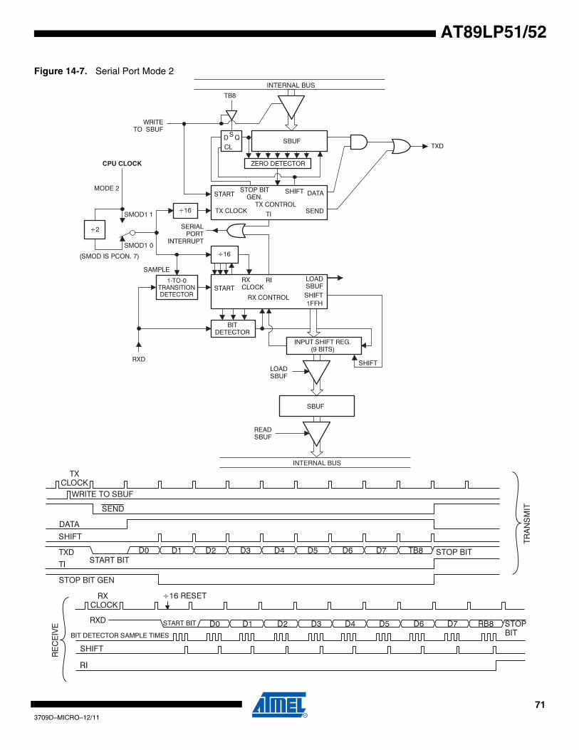
713709D–MICRO–12/11
AT89LP51/52
Figure 14-7. Serial Port Mode 2
SMOD1 1
SMOD1 0
INTERNAL BUS
INTERNAL BUS
CPU CLOCK
723709D–MICRO–12/11
AT89LP51/52
Figure 14-8. Serial Port Mode 3
TXCLOCK
WRITE TO SBUF
SEND
DATA
SHIFT
TXD
STOP BIT GEN
TI
D0 D1 D2 D3 D4 D5 D6 D7 TB8 STOP BIT
TR
AN
SM
IT
START BIT
INTERNAL BUS
READSBUF
LOADSBUF
SBUF
SHIFT
INPUT SHIFT REG.(9 BITS)
BITDETECTOR
1-TO-0TRANSITIONDETECTOR
SERIALPORT
INTERRUPT
WRITETO
SBUF÷2
SMOD1
TIMER 1OVERFLOW
RXD
RX CLOCK
RX CLOCK
RX CONTROLSTART
START DATA
SAMPLE
÷16
÷16
TX CONTROL
TI
ZERO DETECTOR
SBUFTXD
INTERNAL BUS
TB8
D QCL
S
LOADSBUFSHIFT1FFH
SHIFT
RI
SEND
D0 D1 D2 D3 D4 D5 D6 D7 RB8START BIT STOPBIT
÷16 RESETRXCLOCK
BIT DETECTOR SAMPLE TIMES
SHIFT
RE
CE
IVE
RXD
RI
STOP BIT
TIMER 2OVERFLOW
TCLK
RCLK
“0”
“0”
“1”
“1”
“0” “1”
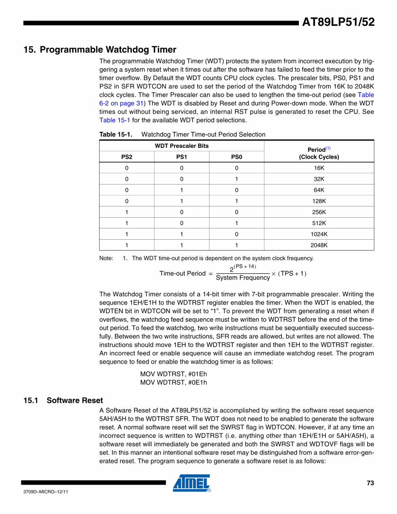
733709D–MICRO–12/11
AT89LP51/52
15. Programmable Watchdog TimerThe programmable Watchdog Timer (WDT) protects the system from incorrect execution by trig-gering a system reset when it times out after the software has failed to feed the timer prior to thetimer overflow. By Default the WDT counts CPU clock cycles. The prescaler bits, PS0, PS1 andPS2 in SFR WDTCON are used to set the period of the Watchdog Timer from 16K to 2048Kclock cycles. The Timer Prescaler can also be used to lengthen the time-out period (see Table6-2 on page 31) The WDT is disabled by Reset and during Power-down mode. When the WDTtimes out without being serviced, an internal RST pulse is generated to reset the CPU. SeeTable 15-1 for the available WDT period selections.
Note: 1. The WDT time-out period is dependent on the system clock frequency.
The Watchdog Timer consists of a 14-bit timer with 7-bit programmable prescaler. Writing thesequence 1EH/E1H to the WDTRST register enables the timer. When the WDT is enabled, theWDTEN bit in WDTCON will be set to “1”. To prevent the WDT from generating a reset when ifoverflows, the watchdog feed sequence must be written to WDTRST before the end of the time-out period. To feed the watchdog, two write instructions must be sequentially executed success-fully. Between the two write instructions, SFR reads are allowed, but writes are not allowed. Theinstructions should move 1EH to the WDTRST register and then 1EH to the WDTRST register.An incorrect feed or enable sequence will cause an immediate watchdog reset. The programsequence to feed or enable the watchdog timer is as follows:
MOV WDTRST, #01EhMOV WDTRST, #0E1h
15.1 Software ResetA Software Reset of the AT89LP51/52 is accomplished by writing the software reset sequence5AH/A5H to the WDTRST SFR. The WDT does not need to be enabled to generate the softwarereset. A normal software reset will set the SWRST flag in WDTCON. However, if at any time anincorrect sequence is written to WDTRST (i.e. anything other than 1EH/E1H or 5AH/A5H), asoftware reset will immediately be generated and both the SWRST and WDTOVF flags will beset. In this manner an intentional software reset may be distinguished from a software error-gen-erated reset. The program sequence to generate a software reset is as follows:
Table 15-1. Watchdog Timer Time-out Period Selection
WDT Prescaler BitsPeriod(1)
(Clock Cycles)PS2 PS1 PS0
0 0 0 16K
0 0 1 32K
0 1 0 64K
0 1 1 128K
1 0 0 256K
1 0 1 512K
1 1 0 1024K
1 1 1 2048K
Time-out Period2
PS 14+( )
System Frequency-------------------------------------------------- TPS 1+( )×=
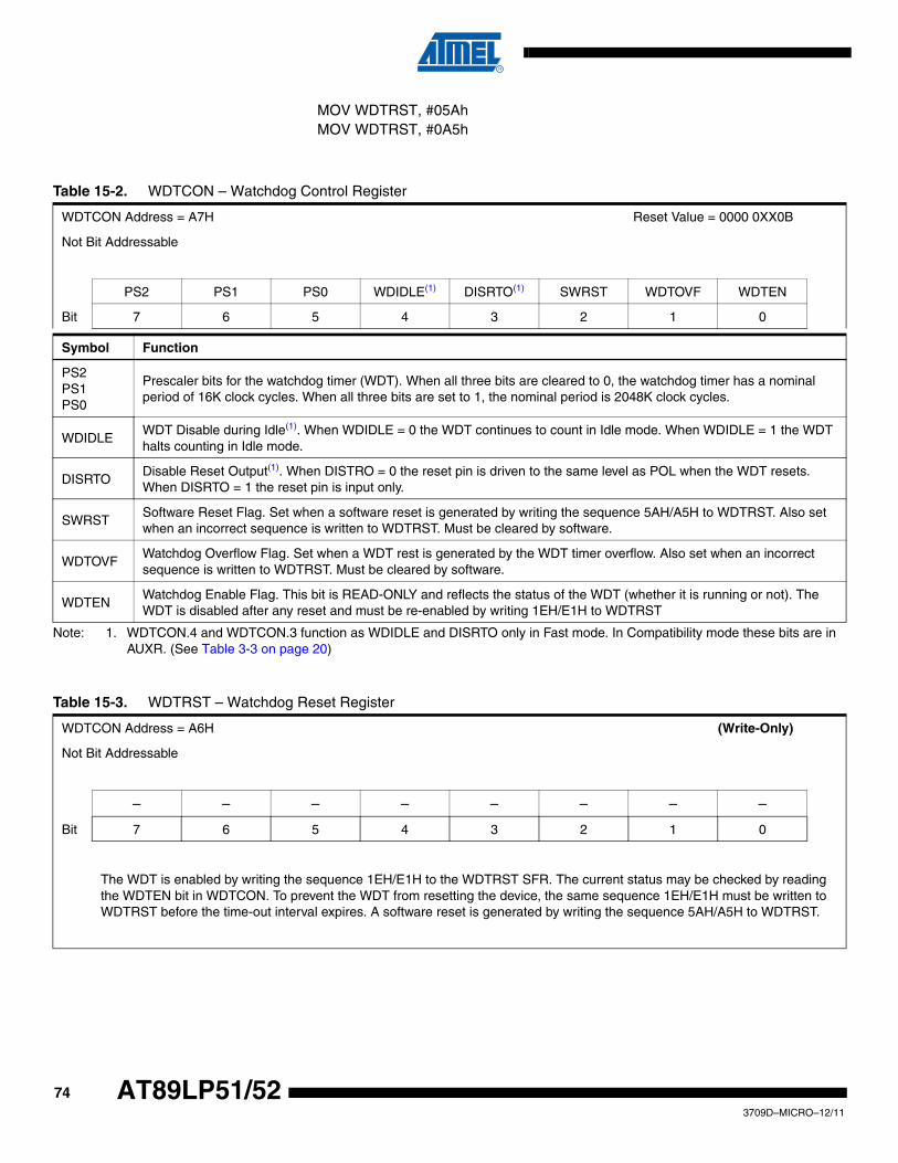
743709D–MICRO–12/11
AT89LP51/52
MOV WDTRST, #05AhMOV WDTRST, #0A5h
Note: 1. WDTCON.4 and WDTCON.3 function as WDIDLE and DISRTO only in Fast mode. In Compatibility mode these bits are in AUXR. (See Table 3-3 on page 20)
Table 15-2. WDTCON – Watchdog Control Register
WDTCON Address = A7H Reset Value = 0000 0XX0B
Not Bit Addressable
PS2 PS1 PS0 WDIDLE(1) DISRTO(1) SWRST WDTOVF WDTEN
Bit 7 6 5 4 3 2 1 0
Symbol Function
PS2PS1PS0
Prescaler bits for the watchdog timer (WDT). When all three bits are cleared to 0, the watchdog timer has a nominal period of 16K clock cycles. When all three bits are set to 1, the nominal period is 2048K clock cycles.
WDIDLEWDT Disable during Idle(1). When WDIDLE = 0 the WDT continues to count in Idle mode. When WDIDLE = 1 the WDT halts counting in Idle mode.
DISRTODisable Reset Output(1). When DISTRO = 0 the reset pin is driven to the same level as POL when the WDT resets. When DISRTO = 1 the reset pin is input only.
SWRSTSoftware Reset Flag. Set when a software reset is generated by writing the sequence 5AH/A5H to WDTRST. Also set when an incorrect sequence is written to WDTRST. Must be cleared by software.
WDTOVFWatchdog Overflow Flag. Set when a WDT rest is generated by the WDT timer overflow. Also set when an incorrect sequence is written to WDTRST. Must be cleared by software.
WDTENWatchdog Enable Flag. This bit is READ-ONLY and reflects the status of the WDT (whether it is running or not). The WDT is disabled after any reset and must be re-enabled by writing 1EH/E1H to WDTRST
Table 15-3. WDTRST – Watchdog Reset Register
WDTCON Address = A6H (Write-Only)
Not Bit Addressable
– – – – – – – –
Bit 7 6 5 4 3 2 1 0
The WDT is enabled by writing the sequence 1EH/E1H to the WDTRST SFR. The current status may be checked by reading the WDTEN bit in WDTCON. To prevent the WDT from resetting the device, the same sequence 1EH/E1H must be written to WDTRST before the time-out interval expires. A software reset is generated by writing the sequence 5AH/A5H to WDTRST.
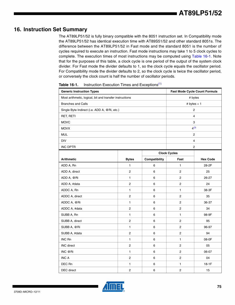
753709D–MICRO–12/11
AT89LP51/52
16. Instruction Set SummaryThe AT89LP51/52 is fully binary compatible with the 8051 instruction set. In Compatibility modethe AT89LP51/52 has identical execution time with AT89S51/52 and other standard 8051s. Thedifference between the AT89LP51/52 in Fast mode and the standard 8051 is the number ofcycles required to execute an instruction. Fast mode instructions may take 1 to 5 clock cycles tocomplete. The execution times of most instructions may be computed using Table 16-1. Notethat for the purposes of this table, a clock cycle is one period of the output of the system clockdivider. For Fast mode the divider defaults to 1, so the clock cycle equals the oscillator period.For Compatibility mode the divider defaults to 2, so the clock cycle is twice the oscillator period,or conversely the clock count is half the number of oscillator periods.
Table 16-1. Instruction Execution Times and Exceptions(1)
Generic Instruction Types Fast Mode Cycle Count Formula
Most arithmetic, logical, bit and transfer instructions # bytes
Branches and Calls # bytes + 1
Single Byte Indirect (i.e. ADD A, @Ri, etc.) 2
RET, RETI 4
MOVC 3
MOVX 4(3)
MUL 2
DIV 4
INC DPTR 2
Arithmetic Bytes
Clock Cycles
Hex CodeCompatibility Fast
ADD A, Rn 1 6 1 28-2F
ADD A, direct 2 6 2 25
ADD A, @Ri 1 6 2 26-27
ADD A, #data 2 6 2 24
ADDC A, Rn 1 6 1 38-3F
ADDC A, direct 2 6 2 35
ADDC A, @Ri 1 6 2 36-37
ADDC A, #data 2 6 2 34
SUBB A, Rn 1 6 1 98-9F
SUBB A, direct 2 6 2 95
SUBB A, @Ri 1 6 2 96-97
SUBB A, #data 2 6 2 94
INC Rn 1 6 1 08-0F
INC direct 2 6 2 05
INC @Ri 1 6 2 06-07
INC A 2 6 2 04
DEC Rn 1 6 1 18-1F
DEC direct 2 6 2 15
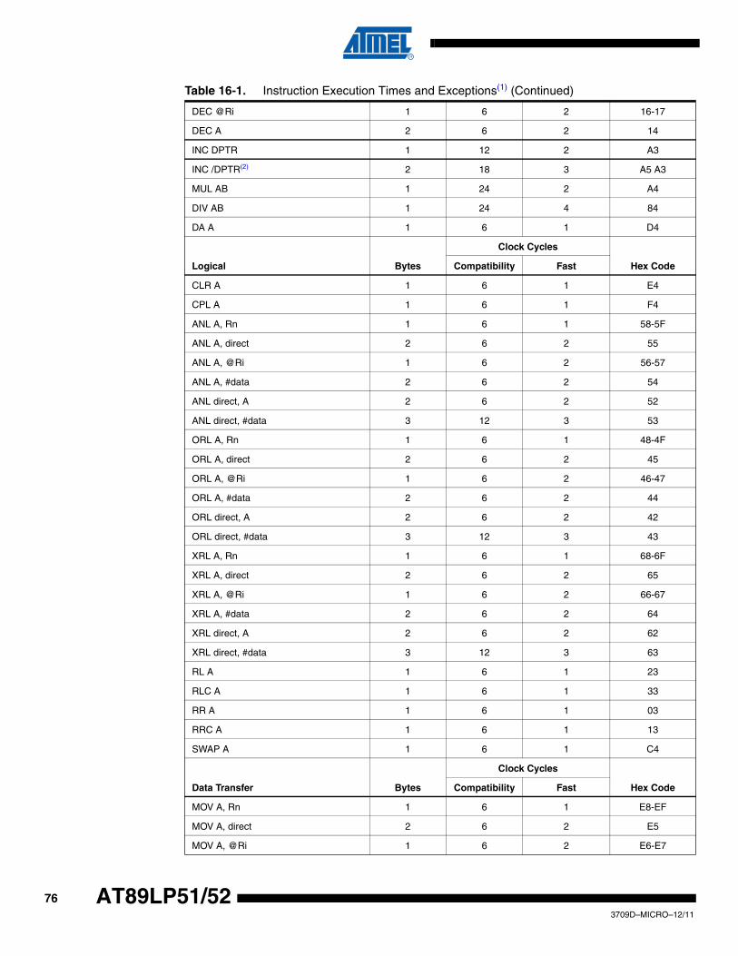
763709D–MICRO–12/11
AT89LP51/52
DEC @Ri 1 6 2 16-17
DEC A 2 6 2 14
INC DPTR 1 12 2 A3
INC /DPTR(2) 2 18 3 A5 A3
MUL AB 1 24 2 A4
DIV AB 1 24 4 84
DA A 1 6 1 D4
Logical Bytes
Clock Cycles
Hex CodeCompatibility Fast
CLR A 1 6 1 E4
CPL A 1 6 1 F4
ANL A, Rn 1 6 1 58-5F
ANL A, direct 2 6 2 55
ANL A, @Ri 1 6 2 56-57
ANL A, #data 2 6 2 54
ANL direct, A 2 6 2 52
ANL direct, #data 3 12 3 53
ORL A, Rn 1 6 1 48-4F
ORL A, direct 2 6 2 45
ORL A, @Ri 1 6 2 46-47
ORL A, #data 2 6 2 44
ORL direct, A 2 6 2 42
ORL direct, #data 3 12 3 43
XRL A, Rn 1 6 1 68-6F
XRL A, direct 2 6 2 65
XRL A, @Ri 1 6 2 66-67
XRL A, #data 2 6 2 64
XRL direct, A 2 6 2 62
XRL direct, #data 3 12 3 63
RL A 1 6 1 23
RLC A 1 6 1 33
RR A 1 6 1 03
RRC A 1 6 1 13
SWAP A 1 6 1 C4
Data Transfer Bytes
Clock Cycles
Hex CodeCompatibility Fast
MOV A, Rn 1 6 1 E8-EF
MOV A, direct 2 6 2 E5
MOV A, @Ri 1 6 2 E6-E7
Table 16-1. Instruction Execution Times and Exceptions(1) (Continued)
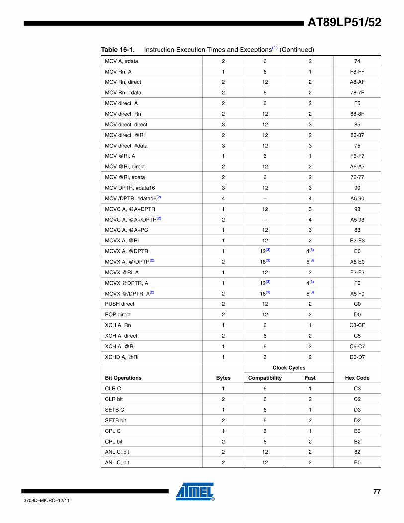
773709D–MICRO–12/11
AT89LP51/52
MOV A, #data 2 6 2 74
MOV Rn, A 1 6 1 F8-FF
MOV Rn, direct 2 12 2 A8-AF
MOV Rn, #data 2 6 2 78-7F
MOV direct, A 2 6 2 F5
MOV direct, Rn 2 12 2 88-8F
MOV direct, direct 3 12 3 85
MOV direct, @Ri 2 12 2 86-87
MOV direct, #data 3 12 3 75
MOV @Ri, A 1 6 1 F6-F7
MOV @Ri, direct 2 12 2 A6-A7
MOV @Ri, #data 2 6 2 76-77
MOV DPTR, #data16 3 12 3 90
MOV /DPTR, #data16(2) 4 – 4 A5 90
MOVC A, @A+DPTR 1 12 3 93
MOVC A, @A+/DPTR(2) 2 – 4 A5 93
MOVC A, @A+PC 1 12 3 83
MOVX A, @Ri 1 12 2 E2-E3
MOVX A, @DPTR 1 12(3) 4(3) E0
MOVX A, @/DPTR(2) 2 18(3) 5(3) A5 E0
MOVX @Ri, A 1 12 2 F2-F3
MOVX @DPTR, A 1 12(3) 4(3) F0
MOVX @/DPTR, A(2) 2 18(3) 5(3) A5 F0
PUSH direct 2 12 2 C0
POP direct 2 12 2 D0
XCH A, Rn 1 6 1 C8-CF
XCH A, direct 2 6 2 C5
XCH A, @Ri 1 6 2 C6-C7
XCHD A, @Ri 1 6 2 D6-D7
Bit Operations Bytes
Clock Cycles
Hex CodeCompatibility Fast
CLR C 1 6 1 C3
CLR bit 2 6 2 C2
SETB C 1 6 1 D3
SETB bit 2 6 2 D2
CPL C 1 6 1 B3
CPL bit 2 6 2 B2
ANL C, bit 2 12 2 82
ANL C, bit 2 12 2 B0
Table 16-1. Instruction Execution Times and Exceptions(1) (Continued)
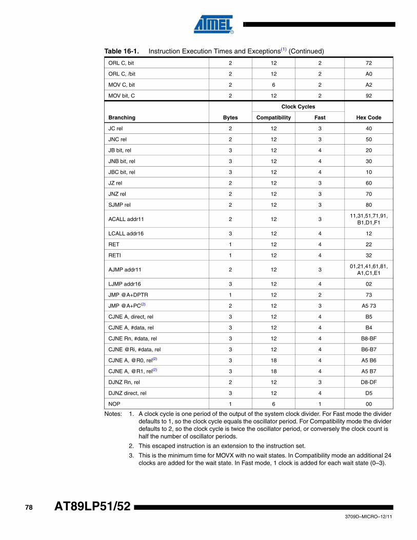
783709D–MICRO–12/11
AT89LP51/52
Notes: 1. A clock cycle is one period of the output of the system clock divider. For Fast mode the divider defaults to 1, so the clock cycle equals the oscillator period. For Compatibility mode the divider defaults to 2, so the clock cycle is twice the oscillator period, or conversely the clock count is half the number of oscillator periods.
2. This escaped instruction is an extension to the instruction set.
3. This is the minimum time for MOVX with no wait states. In Compatibility mode an additional 24 clocks are added for the wait state. In Fast mode, 1 clock is added for each wait state (0–3).
ORL C, bit 2 12 2 72
ORL C, /bit 2 12 2 A0
MOV C, bit 2 6 2 A2
MOV bit, C 2 12 2 92
Branching Bytes
Clock Cycles
Hex CodeCompatibility Fast
JC rel 2 12 3 40
JNC rel 2 12 3 50
JB bit, rel 3 12 4 20
JNB bit, rel 3 12 4 30
JBC bit, rel 3 12 4 10
JZ rel 2 12 3 60
JNZ rel 2 12 3 70
SJMP rel 2 12 3 80
ACALL addr11 2 12 311,31,51,71,91,
B1,D1,F1
LCALL addr16 3 12 4 12
RET 1 12 4 22
RETI 1 12 4 32
AJMP addr11 2 12 301,21,41,61,81,
A1,C1,E1
LJMP addr16 3 12 4 02
JMP @A+DPTR 1 12 2 73
JMP @A+PC(2) 2 12 3 A5 73
CJNE A, direct, rel 3 12 4 B5
CJNE A, #data, rel 3 12 4 B4
CJNE Rn, #data, rel 3 12 4 B8-BF
CJNE @Ri, #data, rel 3 12 4 B6-B7
CJNE A, @R0, rel(2) 3 18 4 A5 B6
CJNE A, @R1, rel(2) 3 18 4 A5 B7
DJNZ Rn, rel 2 12 3 D8-DF
DJNZ direct, rel 3 12 4 D5
NOP 1 6 1 00
Table 16-1. Instruction Execution Times and Exceptions(1) (Continued)
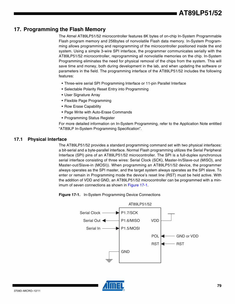
793709D–MICRO–12/11
AT89LP51/52
17. Programming the Flash MemoryThe Atmel AT89LP51/52 microcontroller features 8K bytes of on-chip In-System ProgrammableFlash program memory and 256bytes of nonvolatile Flash data memory. In-System Program-ming allows programming and reprogramming of the microcontroller positioned inside the endsystem. Using a simple 3-wire SPI interface, the programmer communicates serially with theAT89LP51/52 microcontroller, reprogramming all nonvolatile memories on the chip. In-SystemProgramming eliminates the need for physical removal of the chips from the system. This willsave time and money, both during development in the lab, and when updating the software orparameters in the field. The programming interface of the AT89LP51/52 includes the followingfeatures:
• Three-wire serial SPI Programming Interface or 11-pin Parallel Interface
• Selectable Polarity Reset Entry into Programming
• User Signature Array
• Flexible Page Programming
• Row Erase Capability
• Page Write with Auto-Erase Commands
• Programming Status Register
For more detailed information on In-System Programming, refer to the Application Note entitled“AT89LP In-System Programming Specification”.
17.1 Physical InterfaceThe AT89LP51/52 provides a standard programming command set with two physical interfaces:a bit-serial and a byte-parallel interface. Normal Flash programming utilizes the Serial PeripheralInterface (SPI) pins of an AT89LP51/52 microcontroller. The SPI is a full-duplex synchronousserial interface consisting of three wires: Serial Clock (SCK), Master-In/Slave-out (MISO), andMaster-out/Slave-in (MOSI)). When programming an AT89LP51/52 device, the programmeralways operates as the SPI master, and the target system always operates as the SPI slave. Toenter or remain in Programming mode the device’s reset line (RST) must be held active. Withthe addition of VDD and GND, an AT89LP51/52 microcontroller can be programmed with a min-imum of seven connections as shown in Figure 17-1.
Figure 17-1. In-System Programming Device Connections
AT89LP51/52
VDD
RST
P1.7/SCK
P1.5/MOSI
GND
Serial Clock
Serial In
RST
POL
P1.6/MISO Serial Out
GND or VDD
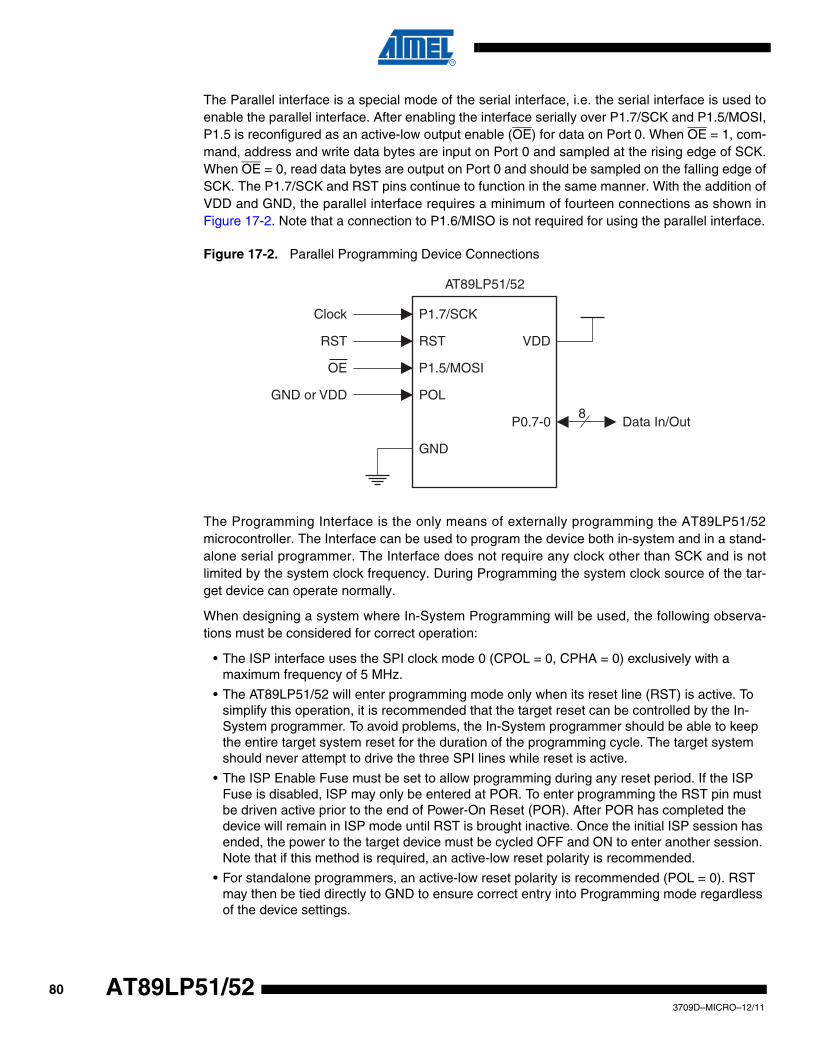
803709D–MICRO–12/11
AT89LP51/52
The Parallel interface is a special mode of the serial interface, i.e. the serial interface is used toenable the parallel interface. After enabling the interface serially over P1.7/SCK and P1.5/MOSI,P1.5 is reconfigured as an active-low output enable (OE) for data on Port 0. When OE = 1, com-mand, address and write data bytes are input on Port 0 and sampled at the rising edge of SCK.When OE = 0, read data bytes are output on Port 0 and should be sampled on the falling edge ofSCK. The P1.7/SCK and RST pins continue to function in the same manner. With the addition ofVDD and GND, the parallel interface requires a minimum of fourteen connections as shown inFigure 17-2. Note that a connection to P1.6/MISO is not required for using the parallel interface.
Figure 17-2. Parallel Programming Device Connections
The Programming Interface is the only means of externally programming the AT89LP51/52microcontroller. The Interface can be used to program the device both in-system and in a stand-alone serial programmer. The Interface does not require any clock other than SCK and is notlimited by the system clock frequency. During Programming the system clock source of the tar-get device can operate normally.
When designing a system where In-System Programming will be used, the following observa-tions must be considered for correct operation:
• The ISP interface uses the SPI clock mode 0 (CPOL = 0, CPHA = 0) exclusively with a maximum frequency of 5 MHz.
• The AT89LP51/52 will enter programming mode only when its reset line (RST) is active. To simplify this operation, it is recommended that the target reset can be controlled by the In-System programmer. To avoid problems, the In-System programmer should be able to keep the entire target system reset for the duration of the programming cycle. The target system should never attempt to drive the three SPI lines while reset is active.
• The ISP Enable Fuse must be set to allow programming during any reset period. If the ISP Fuse is disabled, ISP may only be entered at POR. To enter programming the RST pin must be driven active prior to the end of Power-On Reset (POR). After POR has completed the device will remain in ISP mode until RST is brought inactive. Once the initial ISP session has ended, the power to the target device must be cycled OFF and ON to enter another session. Note that if this method is required, an active-low reset polarity is recommended.
• For standalone programmers, an active-low reset polarity is recommended (POL = 0). RST may then be tied directly to GND to ensure correct entry into Programming mode regardless of the device settings.
AT89LP51/52
VDD RST
P1.7/SCK
P1.5/MOSI
GND
Clock
OE
RST
POLGND or VDD
P0.7-0 Data In/Out 8
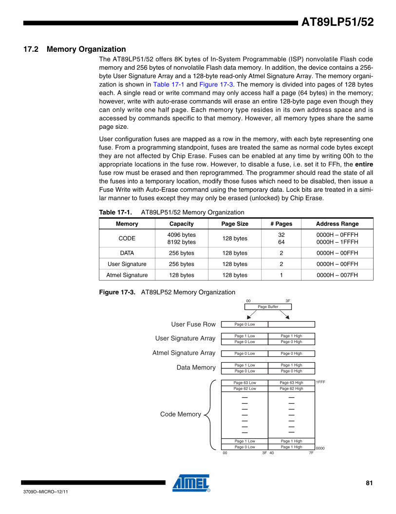
813709D–MICRO–12/11
AT89LP51/52
17.2 Memory OrganizationThe AT89LP51/52 offers 8K bytes of In-System Programmable (ISP) nonvolatile Flash codememory and 256 bytes of nonvolatile Flash data memory. In addition, the device contains a 256-byte User Signature Array and a 128-byte read-only Atmel Signature Array. The memory organi-zation is shown in Table 17-1 and Figure 17-3. The memory is divided into pages of 128 byteseach. A single read or write command may only access half a page (64 bytes) in the memory;however, write with auto-erase commands will erase an entire 128-byte page even though theycan only write one half page. Each memory type resides in its own address space and isaccessed by commands specific to that memory. However, all memory types share the samepage size.
User configuration fuses are mapped as a row in the memory, with each byte representing onefuse. From a programming standpoint, fuses are treated the same as normal code bytes exceptthey are not affected by Chip Erase. Fuses can be enabled at any time by writing 00h to theappropriate locations in the fuse row. However, to disable a fuse, i.e. set it to FFh, the entirefuse row must be erased and then reprogrammed. The programmer should read the state of allthe fuses into a temporary location, modify those fuses which need to be disabled, then issue aFuse Write with Auto-Erase command using the temporary data. Lock bits are treated in a simi-lar manner to fuses except they may only be erased (unlocked) by Chip Erase.
Figure 17-3. AT89LP52 Memory Organization
Table 17-1. AT89LP51/52 Memory Organization
Memory Capacity Page Size # Pages Address Range
CODE4096 bytes8192 bytes
128 bytes3264
0000H – 0FFFH0000H – 1FFFH
DATA 256 bytes 128 bytes 2 0000H – 00FFH
User Signature 256 bytes 128 bytes 2 0000H – 00FFH
Atmel Signature 128 bytes 128 bytes 1 0000H – 007FH
Page 63 Low
Page 62 Low
User Fuse Row
User Signature Array
Atmel Signature Array
Code Memory
00 3F 0000
1FFF
Data Memory
Page 63 High
Page 62 High
40 7F
Page 0 Low
Page 0 Low
Page 1 Low
Page 0 High
Page 1 High
Page 0 Low
Page 1 Low
Page 0 Low
Page 1 High
Page 1 High
Page 0 High
00 3F
Page Buffer
Page 0 Low
Page 1 Low
Page 0 High
Page 1 High
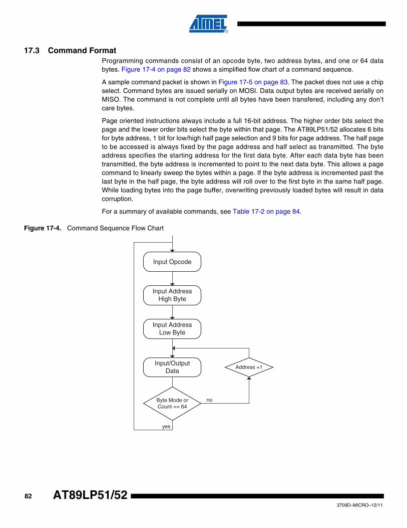
823709D–MICRO–12/11
AT89LP51/52
17.3 Command FormatProgramming commands consist of an opcode byte, two address bytes, and one or 64 databytes. Figure 17-4 on page 82 shows a simplified flow chart of a command sequence.
A sample command packet is shown in Figure 17-5 on page 83. The packet does not use a chipselect. Command bytes are issued serially on MOSI. Data output bytes are received serially onMISO. The command is not complete until all bytes have been transfered, including any don’tcare bytes.
Page oriented instructions always include a full 16-bit address. The higher order bits select thepage and the lower order bits select the byte within that page. The AT89LP51/52 allocates 6 bitsfor byte address, 1 bit for low/high half page selection and 9 bits for page address. The half pageto be accessed is always fixed by the page address and half select as transmitted. The byteaddress specifies the starting address for the first data byte. After each data byte has beentransmitted, the byte address is incremented to point to the next data byte. This allows a pagecommand to linearly sweep the bytes within a page. If the byte address is incremented past thelast byte in the half page, the byte address will roll over to the first byte in the same half page.While loading bytes into the page buffer, overwriting previously loaded bytes will result in datacorruption.
For a summary of available commands, see Table 17-2 on page 84.
Figure 17-4. Command Sequence Flow Chart
Input Opcode
Input Address High Byte
Input Address Low Byte
Input/Output Data
Address +1
Byte Mode orCount == 64
yes
no
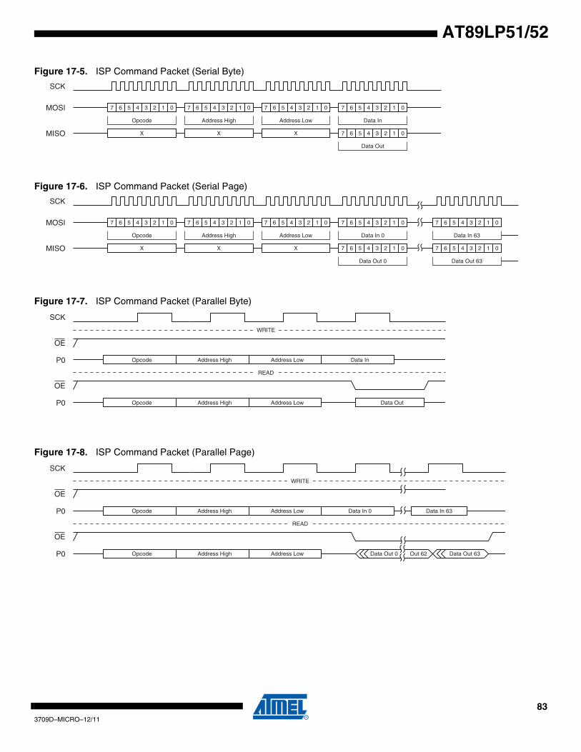
833709D–MICRO–12/11
AT89LP51/52
Figure 17-5. ISP Command Packet (Serial Byte)
Figure 17-6. ISP Command Packet (Serial Page)
Figure 17-7. ISP Command Packet (Parallel Byte)
Figure 17-8. ISP Command Packet (Parallel Page)
7 06 5 4 3 2 1 7 06 5 4 3 2 1 7 06 5 4 3 2 1 7 06 5 4 3 2 1
7 06 5 4 3 2 1
SCK
MOSI
MISO
Opcode Address High Address Low Data In
Data Out
X X X
7 06 5 4 3 2 1 7 06 5 4 3 2 1 7 06 5 4 3 2 1 7 06 5 4 3 2 1
7 06 5 4 3 2 1
SCK
MOSI
MISO
Opcode Address High Address Low Data In 0
Data Out 0
X X X
7 06 5 4 3 2 1
7 06 5 4 3 2 1
Data In 63
Data Out 63
SCK
P0 Opcode Address High Address Low Data In
OE
WRITE
P0 Opcode Address High Address Low Data Out
OE
READ
SCK
P0 Opcode Address High Address Low Data In 0
OE
WRITE
P0 Opcode Address High Address Low Data Out 0
OE
READ
Data In 63
Data Out 63Out 62
843709D–MICRO–12/11
AT89LP51/52
Notes: 1. Program Enable must be the first command issued after entering into programming mode.
2. 0110 1001B is returned on MISO when Program Enable was successful.
3. Parallel Enable switches the interface from serial to parallel format until RST goes inactive.
4. Each byte address selects one fuse or lock bit. Data bytes must be 00h or FFh.
5. See Table 17-5 on page 86 for Fuse definitions.
6. See Table 17-4 on page 86 for Lock Bit definitions.
Table 17-2. Programming Command Summary
Command Opcode Addr High Addr Low Data 0 Data 1–63
Program Enable(1) 1010 1100 0101 0011 xxxx xxxxxxxx xxxx
(0110 1001)(2) –
Parallel Enable(3) 1010 1100 0011 0101 xxxx xxxx xxxx xxxx –
Chip Erase 1010 1100 100x xxxx xxxx xxxx xxxx xxxx –
Read Status 0110 0000 xxxx xxxx xxxx xxxx Status Out –
Write Code Byte 0100 0000 000a aaaa asbb bbbb Data In –
Read Code Byte 0010 0000 000a aaaa asbb bbbb Data Out –
Write Code Page 0101 0000 000a aaaa as00 0000 Byte 0 Bytes 1–63
Write Code Page with Auto-Erase 0111 0000 000a aaaa as00 0000 Byte 0 Bytes 1–63
Read Code Page 0011 0000 000a aaaa as00 0000 Byte 0 Bytes 1–63
Write Data Byte 1100 0000 xxxx xxxx asbb bbbb Data In –
Read Data Byte 1010 0000 xxxx xxxx asbb bbbb Data Out –
Write Data Page 1101 0000 xxxx xxxx as00 0000 Byte 0 Bytes 1–63
Write Data Page with Auto-Erase 1101 0010 xxxx xxxx as00 0000 Byte 0 Bytes 1–63
Read Data Page 1011 0000 xxxx xxxx as00 0000 Byte 0 Bytes 1–63
Write User Fuse(5) 0100 0001 xxxx xxxx 00bb bbbb Fuse In(4) –
Read User Fuse(5) 0010 0001 xxxx xxxx 00bb bbbb Fuse Out(4) –
Write User Fuses(5) 0101 0001 xxxx xxxx 0000 0000 Fuse 0(4) Bytes 1–63
Write User Fuses with Auto-Erase(5) 0111 0001 xxxx xxxx 0000 0000 Fuse 0(4) Fuses 1–63(4)
Read User Fuses(5) 0011 0001 xxxx xxxx 0000 0000 Fuse 0(4) Fuses 1–63(4)
Write Lock Mode(6) 1010 1100 1110 00BB xxxx xxxx xxxx xxxx –
Read Lock Mode(6) 0010 0100 xxxx xxxx xxxx xxxx xxxL LLxx –
Write Lock Bit(6) 0100 0100 xxxx xxxx 00bb bbbb Data In(4) –
Write Lock Bits(6) 0101 0100 xxxx xxxx 0000 0000 Byte 0(4) Bytes 1–63(4)
Read Lock Bits(6) 0011 0100 xxxx xxxx 0000 0000 Byte 0(4) Bytes 1–63(4)
Write User Signature Byte 0100 0010 xxxx xxxx asbb bbbb Data In –
Read User Signature Byte 0010 0010 xxxx xxxx asbb bbbb Data Out –
Write User Signature Page 0101 0010 xxxx xxxx as00 0000 Byte 0 Byte 1–63
Write User Signature Page with Auto-Erase 0111 0010 xxxx xxxx as00 0000 Byte 0 Byte 1–63
Read User Signature Page 0011 0010 xxxx xxxx as00 0000 Byte 0 Byte 1–63
Read Atmel Signature Byte(7) 0010 1000 xxxx xxxx 0sbb bbbb Data Out –
Read Atmel Signature Page(7) 0011 1000 xxxx xxxx 0s00 0000 Byte 0 Byte 1–63
853709D–MICRO–12/11
AT89LP51/52
7. Atmel Signature Bytes:
8. Symbol Key:
17.4 Status RegisterThe current state of the memory may be accessed by reading the status register. The status reg-ister is shown in Table 17-3.
17.5 DATA PollingThe AT89LP51/52 implements DATA polling to indicate the end of a programming cycle. Whilethe device is busy, any attempted read of the last byte written will return the data byte with theMSB complemented. Once the programming cycle has completed, the true value will be acces-sible. During Erase the data is assumed to be FFH and DATA polling will return 7FH. Whenwriting multiple bytes in a page, the DATA value will be the last data byte loaded before pro-gramming begins, not the written byte with the highest physical address within the page.
17.6 Flash SecurityThe AT89LP51/52 provides three Lock Bits for Flash Code and Data Memory security. Lock bitscan be left unprogrammed (FFh) or programmed (00h) to obtain the protection levels listed inTable 17-4. Lock bits can only be erased (set to FFh) by Chip Erase. Lock bit mode 2 disablesprogramming of all memory spaces, including the User Signature Array and User ConfigurationFuses. User fuses must be programmed before enabling Lock bit mode 2 or 3. Lock bit mode 3
Address: 0000H 0001H 0002H
AT89LP51: 1EH 54H 05H
AT89LP52: 1EH 54H 06H
a: Page Address Bit
s: Half Page Select Bit
b: Byte Address Bit
x: Don’t Care Bit
Table 17-3. Status Register
– – – – LOAD SUCCESS WRTINH BUSY
Bit 7 6 5 4 3 2 1 0
Symbol Function
LOADLoad flag. Cleared low by the load page buffer command and set high by the next memory write. This flag signals that the page buffer was previously loaded with data by the load page buffer command.
SUCCESSSuccess flag. Cleared low at the start of a programming cycle and will only be set high if the programming cycle completes without interruption from the brownout detector.
WRTINHWrite Inhibit flag. Cleared low by the brownout detector (BOD) whenever programming is inhibited due to VDD falling below the minimum required programming voltage. If a BOD episode occurs during programming, the SUCCESS flag will remain low after the cycle is complete.
BUSY Busy flag. Cleared low whenever the memory is busy programming or if write is currently inhibited.
863709D–MICRO–12/11
AT89LP51/52
implements mode 2 and also blocks reads from the code and data memories; however, reads ofthe User Signature Array, Atmel Signature Array, and User Configuration Fuses are still allowed.
The Lock Bits will not disable FDATA or IAP programming initiated by the application software.
17.7 User Configuration FusesThe AT89LP51/52 includes 10 user fuses for configuration of the device. Each fuse is accessedat a separate address in the User Fuse Row as listed in Table 17-5. Fuses are cleared by pro-gramming 00h to their locations. Programming FFh to a fuse location will cause that fuse tomaintain its previous state. To set a fuse (set to FFh) the fuse row must be erased and thenreprogrammed using the Fuse Write with Auto-erase command. The default state for all fuses isFFh except for Tristate Ports, which defaults to 00h.
Table 17-4. Lock Bit Protection Modes
Program Lock Bits (by address)
Mode 00h 01h 02h Protection Mode
1 FFh FFh FFh No program lock features
2 00h FFh FFh Further programming of the Flash is disabled
3 00h 00h FFh Further programming of the Flash is disabled and verify (read) is also disabled
4 00h 00h 00hFurther programming of the Flash is disabled and verify (read) is also disabled; External execution above 4K/8K is disabled
Table 17-5. User Configuration Fuse Definitions
Address Fuse Name Description
00 – 01h Clock Source – CS[0:1](2)
Selects source for the system clock:
CS1 CS0 Selected Source
FFh FFh High Speed Crystal Oscillator (XTAL)
FFh 00h Low Speed Crystal Oscillator (XTAL)
00h FFh External Clock on XTAL1 (XCLK)
00h 00h Internal Auxiliary Oscillator (IRC)
02 – 03h Start-up Time – SUT[0:1]
Selects time-out delay for the POR/BOD/PWD wake-up period:
SUT1 SUT0 Selected Time-out
00h 00h 1 ms (XTAL); 16 µs (XCLK/IRC)
00h FFh 2 ms (XTAL); 512 µs (XCLK/IRC)
FFh 00h 4 ms (XTAL); 1 ms (XCLK/IRC)
FFh FFh 16 ms (XTAL); 4 ms (XCLK/IRC)
04h Compatibility ModeFFh: CPU functions in 12-clock Compatibility mode00h: CPU functions is single-cycle Fast mode
05h ISP Enable(3) FFh: In-System Programming Enabled00h: In-System Programming Disabled (Enabled at POR only)
06H User Signature ProgrammingFFh: Programming of User Signature Disabled00h: Programming of User Signature Enabled
873709D–MICRO–12/11
AT89LP51/52
Notes: 1. The default state for Tristate Ports is 00h. All other fuses default to FFh.
2. Changes to these fuses will only take effect after a device POR.
3. Changes to these fuses will only take effect after the ISP session terminates by bringing RST inactive.
17.8 User SignatureThe User Signature Array contains 256 bytes of non-volatile memory in two 128-byte pages. TheUser Signature is available for serial numbers, firmware revision information, date codes or otheruser parameters. The User Signature Array may only be written by an external device when theUser Signature Programming Fuse is enabled. When the fuse is enabled, Chip Erase will alsoerase the first page of the array. When the fuse is disabled, the array is not affected by write orerase commands. Programming of the Signature Array can also be disabled by the Lock Bits.However, reading the signature is always allowed and the array should not be used to storesecurity sensitive information. The User Signature Array may be modified during executionthrough the In-Application Programming interface, regardless of the state of the User SignatureProgramming fuse or Lock Bits, provided that the IAP Fuse is enabled. Note that the address ofthe User Signature Array, as seen by the IAP interface, equals the User Signature address plus256 (0100H–01FFH instead of 0000H–00FFH).
17.9 Programming Interface TimingThis section details general system timing sequences and constraints for entering or exiting In-System Programming as well as parameters related to the Serial Peripheral Interface duringISP. The general timing parameters for the following waveform figures are listed in section “Tim-ing Parameters” on page 91.
17.9.1 Power-up SequenceExecute this sequence to enter programming mode immediately after power-up. In the RST pinis disabled or if the ISP Fuse is disabled, this is the only method to enter programming (see“External Reset” on page 33).
1. Apply power between VDD and GND pins. RST should remain low.
2. Wait at least tPWRUP. and drive RST high if active-high otherwise keep low.
3. Wait at least tSUT for the internal Power-on Reset to complete. The value of tSUT will depend on the current settings of the device.
4. Start programming session.
07H Tristate PortsFFh: I/O Ports start in input-only mode (tristated) after reset00h: I/O Ports start in quasi-bidirectional mode after reset
08H In-Application ProgrammingFFh: In-Application Programming Disabled00h: In-Application Programming Enabled
09H R1 EnableFFh: 5 MΩ resistor on XTAL1 Disabled00h: 5 MΩ resistor on XTAL1 Enabled
Table 17-5. User Configuration Fuse Definitions
Address Fuse Name Description
883709D–MICRO–12/11
AT89LP51/52
Figure 17-9. Serial Programming Power-up Sequence
17.9.2 Power-down Sequence Execute this sequence to power-down the device after programming.
1. Drive SCK low.
2. Wait at least tSSD and Tristate MOSI.
3. Wait at least tRHZ and drive RST low.
4. Wait at least tSSZ and tristate SCK.
5. Wait no more than tPWRDN and power off VDD.
Figure 17-10. Serial Programming Power-down Sequence
17.9.3 ISP Start Sequence Execute this sequence to exit CPU execution mode and enter ISP mode when the device haspassed Power-On Reset and is already operational.
1. Drive RST high.
2. Wait tRLZ + tSTL.
3. Drive SCK low.
4. Start programming session.
VDD
RST
RST
SCK
HIGH Z MISO
HIGH Z MOSI
tPWRUP
tPOR + tSUT
VDD
RST
SCK
HIGH ZMISO
HIGH ZMOSI
tPWRDN
tSSD tSSZtRHZ
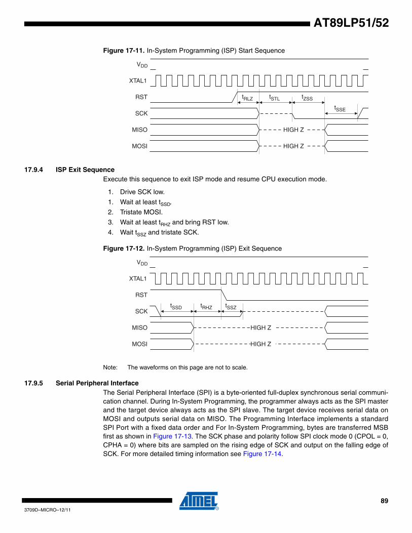
893709D–MICRO–12/11
AT89LP51/52
Figure 17-11. In-System Programming (ISP) Start Sequence
17.9.4 ISP Exit Sequence Execute this sequence to exit ISP mode and resume CPU execution mode.
1. Drive SCK low.
1. Wait at least tSSD.
2. Tristate MOSI.
3. Wait at least tRHZ and bring RST low.
4. Wait tSSZ and tristate SCK.
Figure 17-12. In-System Programming (ISP) Exit Sequence
Note: The waveforms on this page are not to scale.
17.9.5 Serial Peripheral InterfaceThe Serial Peripheral Interface (SPI) is a byte-oriented full-duplex synchronous serial communi-cation channel. During In-System Programming, the programmer always acts as the SPI masterand the target device always acts as the SPI slave. The target device receives serial data onMOSI and outputs serial data on MISO. The Programming Interface implements a standardSPI Port with a fixed data order and For In-System Programming, bytes are transferred MSBfirst as shown in Figure 17-13. The SCK phase and polarity follow SPI clock mode 0 (CPOL = 0,CPHA = 0) where bits are sampled on the rising edge of SCK and output on the falling edge ofSCK. For more detailed timing information see Figure 17-14.
tSTL
VDD
RST
SCK
HIGH ZMOSI
HIGH ZMISO
XTAL1
tRLZ tZSS
tSSE
VDD
RST
SCK
HIGH ZMOSI
HIGH ZMISO
XTAL1
tSSZtSSD tRHZ
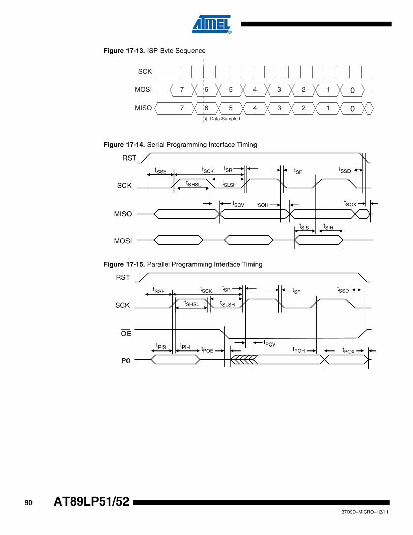
903709D–MICRO–12/11
AT89LP51/52
Figure 17-13. ISP Byte Sequence
Figure 17-14. Serial Programming Interface Timing
Figure 17-15. Parallel Programming Interface Timing
7
7
6
6
5
5
4
4
3
3
2
2
1
1
0
0
MOSI
MISO
SCK
Data Sampled
tSR tSSE
tSLSH
tSOV
tSF
tSOX
tSSD tSCK
tSHSL
tSOH
tSIH tSIS
RST
SCK
MISO
MOSI
tSR tSSE
tSLSH
tSF
tPOX
tSSD tSCK
tSHSL
tPOV tPOE
tPIH tPIS
RST
SCK
P0
OE
tPOH
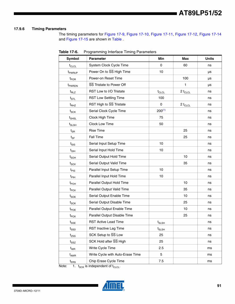
913709D–MICRO–12/11
AT89LP51/52
17.9.6 Timing ParametersThe timing parameters for Figure 17-9, Figure 17-10, Figure 17-11, Figure 17-12, Figure 17-14and Figure 17-15 are shown in Table .
Note: 1. tSCK is independent of tCLCL.
Table 17-6. Programming Interface Timing Parameters
Symbol Parameter Min Max Units
tCLCL System Clock Cycle Time 0 60 ns
tPWRUP Power On to SS High Time 10 µs
tPOR Power-on Reset Time 100 µs
tPWRDN SS Tristate to Power Off 1 µs
tRLZ RST Low to I/O Tristate tCLCL 2 tCLCL ns
tSTL RST Low Settling Time 100 ns
tRHZ RST High to SS Tristate 0 2 tCLCL ns
tSCK Serial Clock Cycle Time 200(1) ns
tSHSL Clock High Time 75 ns
tSLSH Clock Low Time 50 ns
tSR Rise Time 25 ns
tSF Fall Time 25 ns
tSIS Serial Input Setup Time 10 ns
tSIH Serial Input Hold Time 10 ns
tSOH Serial Output Hold Time 10 ns
tSOV Serial Output Valid Time 35 ns
tPIS Parallel Input Setup Time 10 ns
tPIH Parallel Input Hold Time 10 ns
tPOH Parallel Output Hold Time 10 ns
tPOV Parallel Output Valid Time 35 ns
tSOE Serial Output Enable Time 10 ns
tSOX Serial Output Disable Time 25 ns
tPOE Parallel Output Enable Time 10 ns
tPOX Parallel Output Disable Time 25 ns
tSSE RST Active Lead Time tSLSH ns
tSSD RST Inactive Lag Time tSLSH ns
tZSS SCK Setup to SS Low 25 ns
tSSZ SCK Hold after SS High 25 ns
tWR Write Cycle Time 2.5 ms
tAWR Write Cycle with Auto-Erase Time 5 ms
tERS Chip Erase Cycle Time 7.5 ms
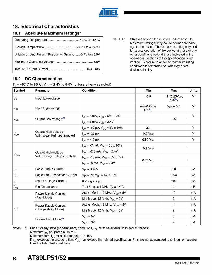
923709D–MICRO–12/11
AT89LP51/52
18. Electrical Characteristics
Notes: 1. Under steady state (non-transient) conditions, IOL must be externally limited as follows:Maximum IOL per port pin: 10 mAMaximum total IOL for all output pins: 100 mAIf IOL exceeds the test condition, VOL may exceed the related specification. Pins are not guaranteed to sink current greater than the listed test conditions.
18.1 Absolute Maximum Ratings*
Operating Temperature ................................... -40°C to +85°C *NOTICE: Stresses beyond those listed under “Absolute Maximum Ratings” may cause permanent dam-age to the device. This is a stress rating only and functional operation of the device at these or any other conditions beyond those indicated in the operational sections of this specification is not implied. Exposure to absolute maximum rating conditions for extended periods may affect device reliability.
Storage Temperature ..................................... -65°C to +150°C
Voltage on Any Pin with Respect to Ground......-0.7V to +5.5V
Maximum Operating Voltage ............................................ 5.5V
Total DC Output Current ........................................... 150.0 mA
18.2 DC CharacteristicsTA = -40°C to 85°C, VDD = 2.4V to 5.5V (unless otherwise noted)
Symbol Parameter Condition Min Max Units
VIL Input Low-voltage-0.5 min(0.25VDD,
0.8(3))V
VIH Input High-voltagemin(0.7VDD,
2.4(3))VDD + 0.5 V
VOL Output Low-voltage(1)IOL = 8 mA, VDD = 5V ± 10%
0.5V
IOL = 4 mA, VDD = 2.4V
VOHOutput High-voltageWith Weak Pull-ups Enabled
IOH = -60 µA, VDD = 5V ± 10% 2.4 V
IOH = -25 µA 0.7 VDD V
IOH = -10 µA 0.85 VDD V
VOH1Output High-voltageWith Strong Pull-ups Enabled
IOH = -7 mA, VDD = 5V ± 10%0.9 VDD
IOH = -2.5 mA, VDD = 2.4V
IOH = -10 mA, VDD = 5V ± 10%0.75 VDD
IOH = -6 mA, VDD = 2.4V
IIL Logic 0 Input Current VIN = 0.45V -50 µA
ITL Logic 1 to 0 Transition Current VIN = 2V, VDD = 5V ± 10% -200 µA
ILI Input Leakage Current 0 < VIN < VDD ±10 µA
CIO Pin Capacitance Test Freq. = 1 MHz, TA = 25°C 10 pF
ICC
Power Supply Current(Fast Mode)
Active Mode, 12 MHz, VDD = 5V 10 mA
Idle Mode, 12 MHz, VDD = 5V 3 mA
Power Supply Current(Compatibility Mode)
Active Mode, 12 MHz, VDD = 5V 4 mA
Idle Mode, 12 MHz, VDD = 5V 2 mA
Power-down Mode(2)VDD = 5V 5 µA
VDD = 3V 2 µA
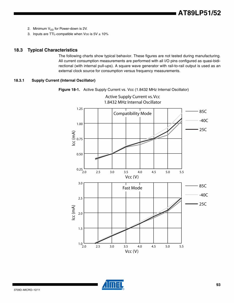
933709D–MICRO–12/11
AT89LP51/52
2. Minimum VDD for Power-down is 2V.
3. Inputs are TTL-compatible when VDD is 5V ± 10%
18.3 Typical CharacteristicsThe following charts show typical behavior. These figures are not tested during manufacturing.All current consumption measurements are performed with all I/O pins configured as quasi-bidi-rectional (with internal pull-ups). A square wave generator with rail-to-rail output is used as anexternal clock source for consumption versus frequency measurements.
18.3.1 Supply Current (Internal Oscillator)
Figure 18-1. Active Supply Current vs. Vcc (1.8432 MHz Internal Oscillator)
2.0 2.5 3.0 3.5 4.0 4.5 5.0 5.50.25
0.50
0.75
1.00
1.2585C
-40C
25C
Vcc (V)
Icc
(mA
)
Active Supply Current vs. Vcc1.8432 MHz Internal Oscillator
Compatibility Mode
2.0 2.5 3.0 3.5 4.0 4.5 5.0 5.51.0
1.5
2.0
2.5
3.085C
-40C
25C
Vcc (V)
Icc
(mA
)
Fast Mode
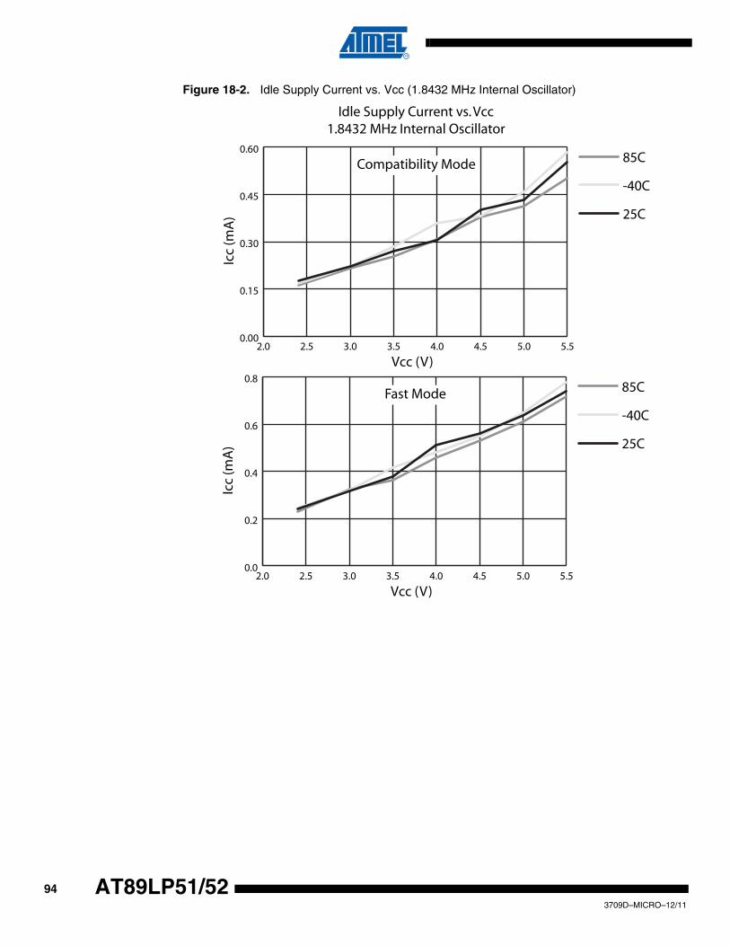
943709D–MICRO–12/11
AT89LP51/52
Figure 18-2. Idle Supply Current vs. Vcc (1.8432 MHz Internal Oscillator)
2.0 2.5 3.0 3.5 4.0 4.5 5.0 5.50.00
0.15
0.30
0.45
0.6085C
-40C
25C
Vcc (V)
Icc
(mA
)
Idle Supply Current vs. Vcc1.8432 MHz Internal Oscillator
Compatibility Mode
2.0 2.5 3.0 3.5 4.0 4.5 5.0 5.50.0
0.2
0.4
0.6
0.885C
-40C
25C
Vcc (V)
Icc
(mA
)
Fast Mode
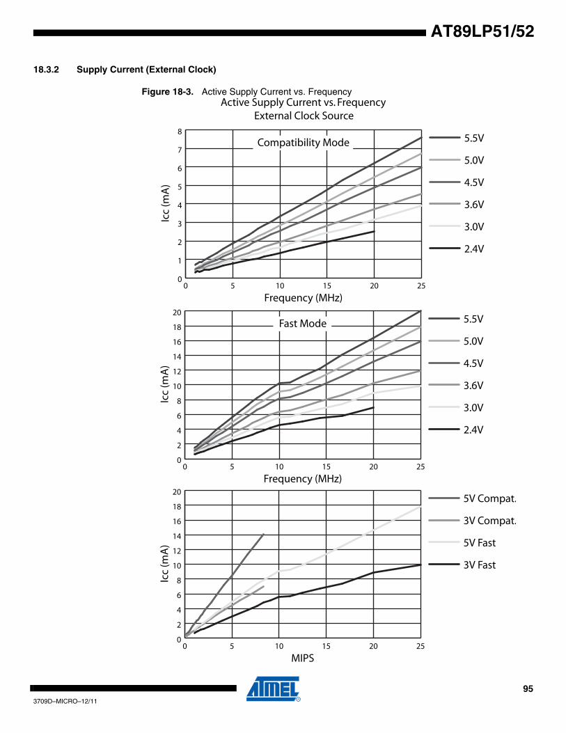
953709D–MICRO–12/11
AT89LP51/52
18.3.2 Supply Current (External Clock)
Figure 18-3. Active Supply Current vs. Frequency
0 5 10 15 20 250
1
2
3
4
5
6
7
85.5V
5.0V
4.5V
3.6V
3.0V
2.4V
Frequency (MHz)
Icc
(mA
)
Active Supply Current vs. Frequency External Clock Source
Compatibility Mode
0 5 10 15 20 250
2
4
6
8
10
12
14
16
18
205.5V
5.0V
4.5V
3.6V
3.0V
2.4V
Frequency (MHz)
Icc
(mA
)
Fast Mode
0 5 10 15 20 250
2
4
6
8
10
12
14
16
18
205V Compat.
3V Compat.
5V Fast
3V Fast
MIPS
Icc
(mA
)
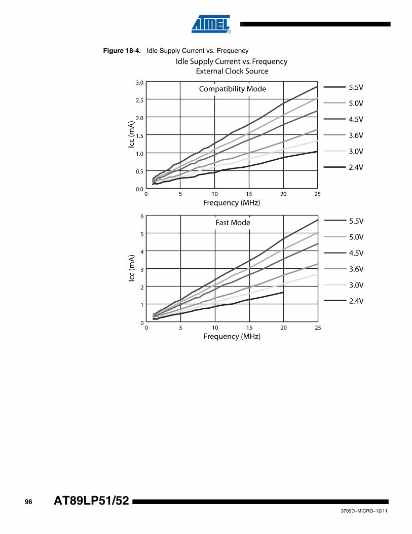
963709D–MICRO–12/11
AT89LP51/52
Figure 18-4. Idle Supply Current vs. Frequency
0 5 10 15 20 250.0
0.5
1.0
1.5
2.0
2.5
3.05.5V
5.0V
4.5V
3.6V
3.0V
2.4V
Frequency (MHz)
Icc
(mA
)
Idle Supply Current vs. Frequency External Clock Source
Compatibility Mode
0 5 10 15 20 250
1
2
3
4
5
65.5V
5.0V
4.5V
3.6V
3.0V
2.4V
Frequency (MHz)
Icc
(mA
)
Fast Mode
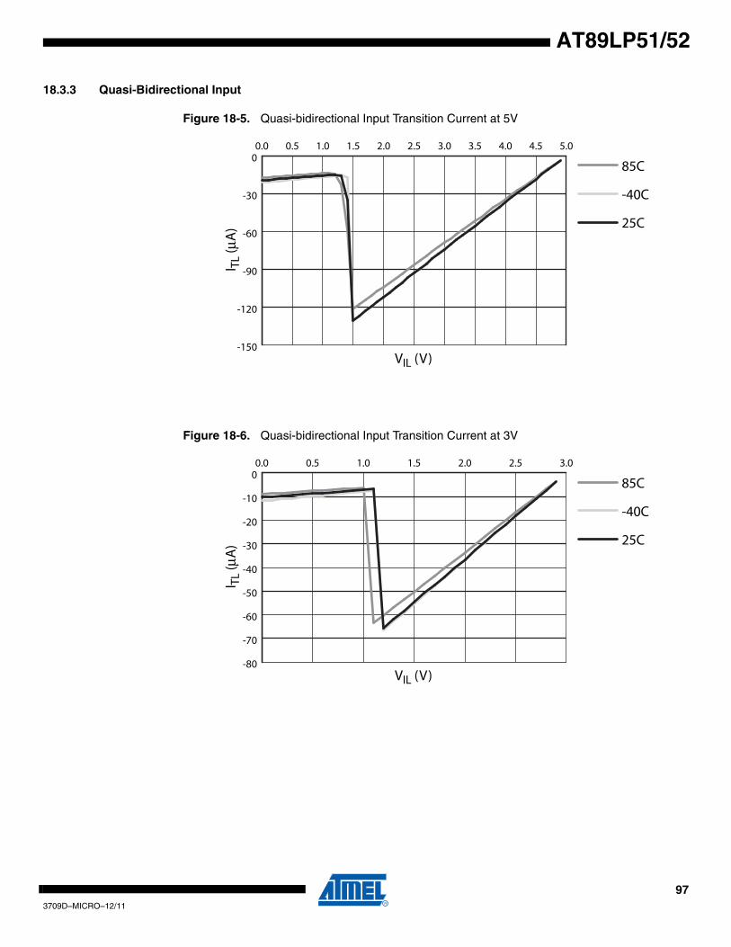
973709D–MICRO–12/11
AT89LP51/52
18.3.3 Quasi-Bidirectional Input
Figure 18-5. Quasi-bidirectional Input Transition Current at 5V
Figure 18-6. Quasi-bidirectional Input Transition Current at 3V
0.0 0.5 1.0 1.5 2.0 2.5 3.0 3.5 4.0 4.5 5.0
-150
-120
-90
-60
-30
085C
-40C
25C
VIL (V)
I TL
(μA
)
0.0 0.5 1.0 1.5 2.0 2.5 3.0
-80
-70
-60
-50
-40
-30
-20
-10
085C
-40C
25C
VIL (V)
I TL
(μA
)
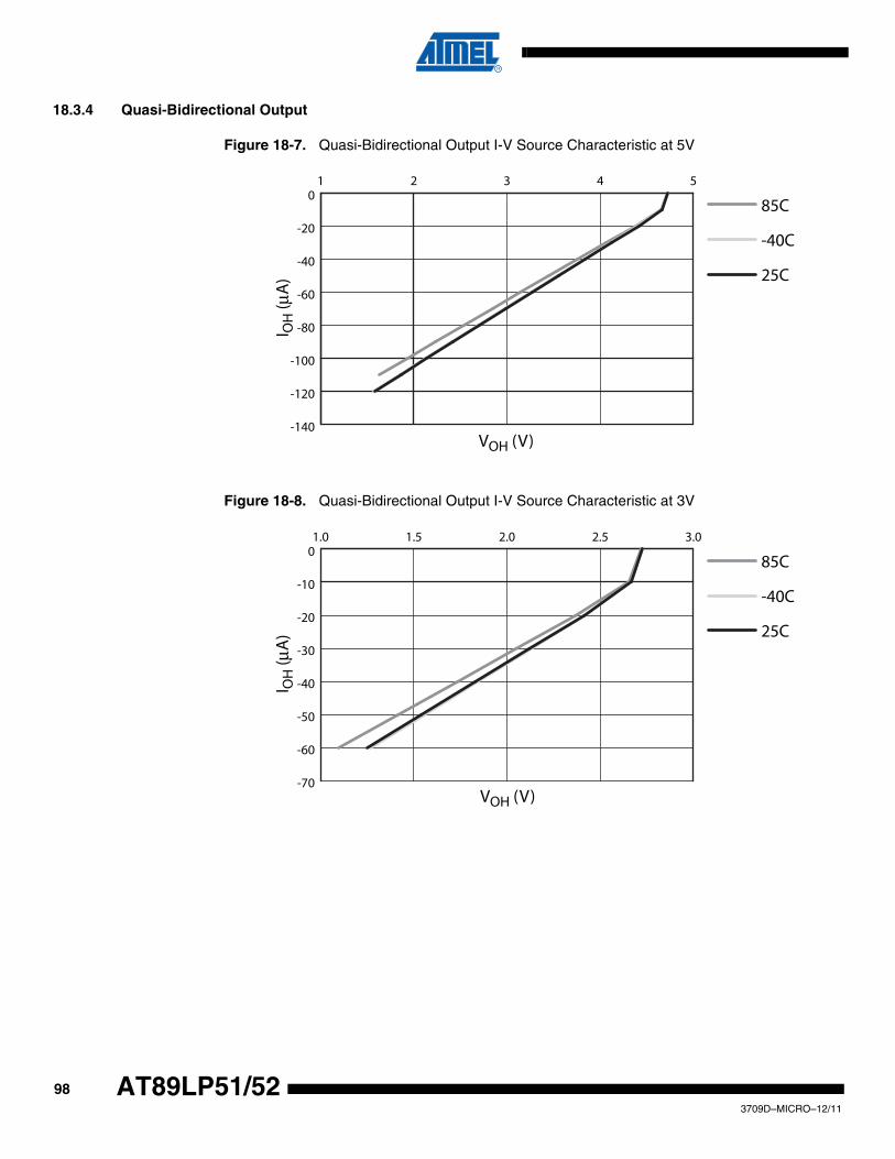
983709D–MICRO–12/11
AT89LP51/52
18.3.4 Quasi-Bidirectional Output
Figure 18-7. Quasi-Bidirectional Output I-V Source Characteristic at 5V
Figure 18-8. Quasi-Bidirectional Output I-V Source Characteristic at 3V
1 2 3 4 5
-140
-120
-100
-80
-60
-40
-20
085C
-40C
25C
VOH (V)
I OH
(μA
)
1.0 1.5 2.0 2.5 3.0
-70
-60
-50
-40
-30
-20
-10
085C
-40C
25C
VOH (V)
I OH
(μA
)
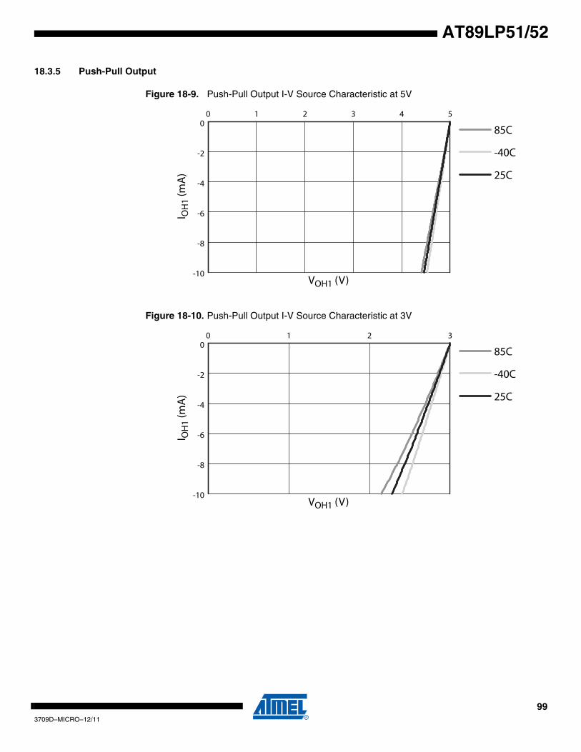
993709D–MICRO–12/11
AT89LP51/52
18.3.5 Push-Pull Output
Figure 18-9. Push-Pull Output I-V Source Characteristic at 5V
Figure 18-10. Push-Pull Output I-V Source Characteristic at 3V
0 1 2 3 4 5
-10
-8
-6
-4
-2
085C
-40C
25C
VOH1 (V)
I OH
1 (m
A)
0 1 2 3
-10
-8
-6
-4
-2
085C
-40C
25C
VOH1 (V)
I OH
1 (m
A)
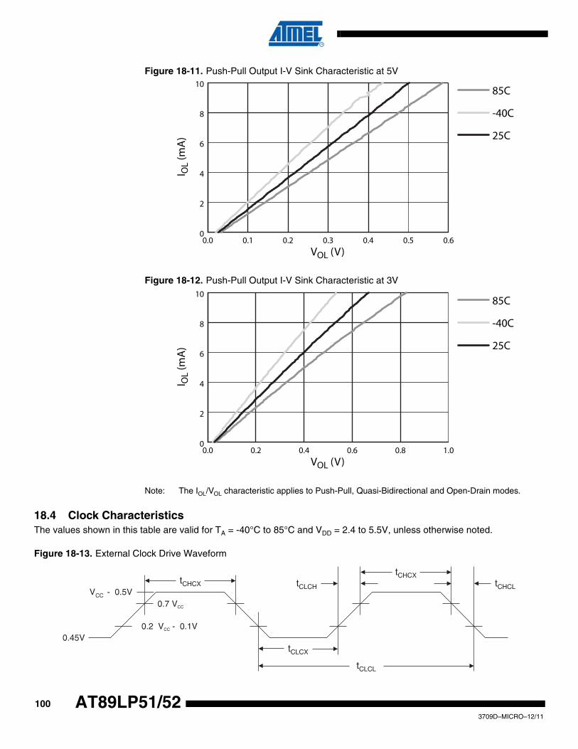
1003709D–MICRO–12/11
AT89LP51/52
Figure 18-11. Push-Pull Output I-V Sink Characteristic at 5V
Figure 18-12. Push-Pull Output I-V Sink Characteristic at 3V
Note: The IOL/VOL characteristic applies to Push-Pull, Quasi-Bidirectional and Open-Drain modes.
18.4 Clock CharacteristicsThe values shown in this table are valid for TA = -40°C to 85°C and VDD = 2.4 to 5.5V, unless otherwise noted.
Figure 18-13. External Clock Drive Waveform
0.0 0.1 0.2 0.3 0.4 0.5 0.60
2
4
6
8
1085C
-40C
25C
VOL (V)
I OL
(mA
)
0.0 0.2 0.4 0.6 0.8 1.00
2
4
6
8
1085C
-40C
25C
VOL (V)
I OL
(mA
)
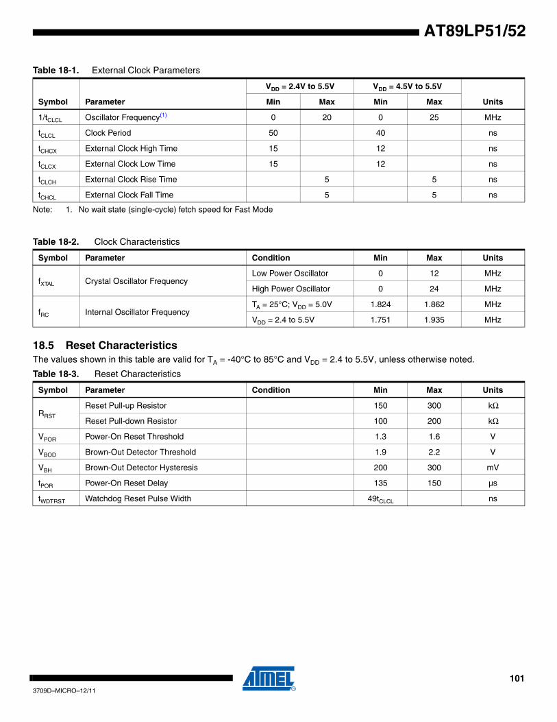
1013709D–MICRO–12/11
AT89LP51/52
Note: 1. No wait state (single-cycle) fetch speed for Fast Mode
18.5 Reset CharacteristicsThe values shown in this table are valid for TA = -40°C to 85°C and VDD = 2.4 to 5.5V, unless otherwise noted.
Table 18-1. External Clock Parameters
Symbol Parameter
VDD = 2.4V to 5.5V VDD = 4.5V to 5.5V
UnitsMin Max Min Max
1/tCLCL Oscillator Frequency(1) 0 20 0 25 MHz
tCLCL Clock Period 50 40 ns
tCHCX External Clock High Time 15 12 ns
tCLCX External Clock Low Time 15 12 ns
tCLCH External Clock Rise Time 5 5 ns
tCHCL External Clock Fall Time 5 5 ns
Table 18-2. Clock Characteristics
Symbol Parameter Condition Min Max Units
fXTAL Crystal Oscillator FrequencyLow Power Oscillator 0 12 MHz
High Power Oscillator 0 24 MHz
fRC Internal Oscillator FrequencyTA = 25°C; VDD = 5.0V 1.824 1.862 MHz
VDD = 2.4 to 5.5V 1.751 1.935 MHz
Table 18-3. Reset Characteristics
Symbol Parameter Condition Min Max Units
RRST
Reset Pull-up Resistor 150 300 kΩ
Reset Pull-down Resistor 100 200 kΩ
VPOR Power-On Reset Threshold 1.3 1.6 V
VBOD Brown-Out Detector Threshold 1.9 2.2 V
VBH Brown-Out Detector Hysteresis 200 300 mV
tPOR Power-On Reset Delay 135 150 µs
tWDTRST Watchdog Reset Pulse Width 49tCLCL ns
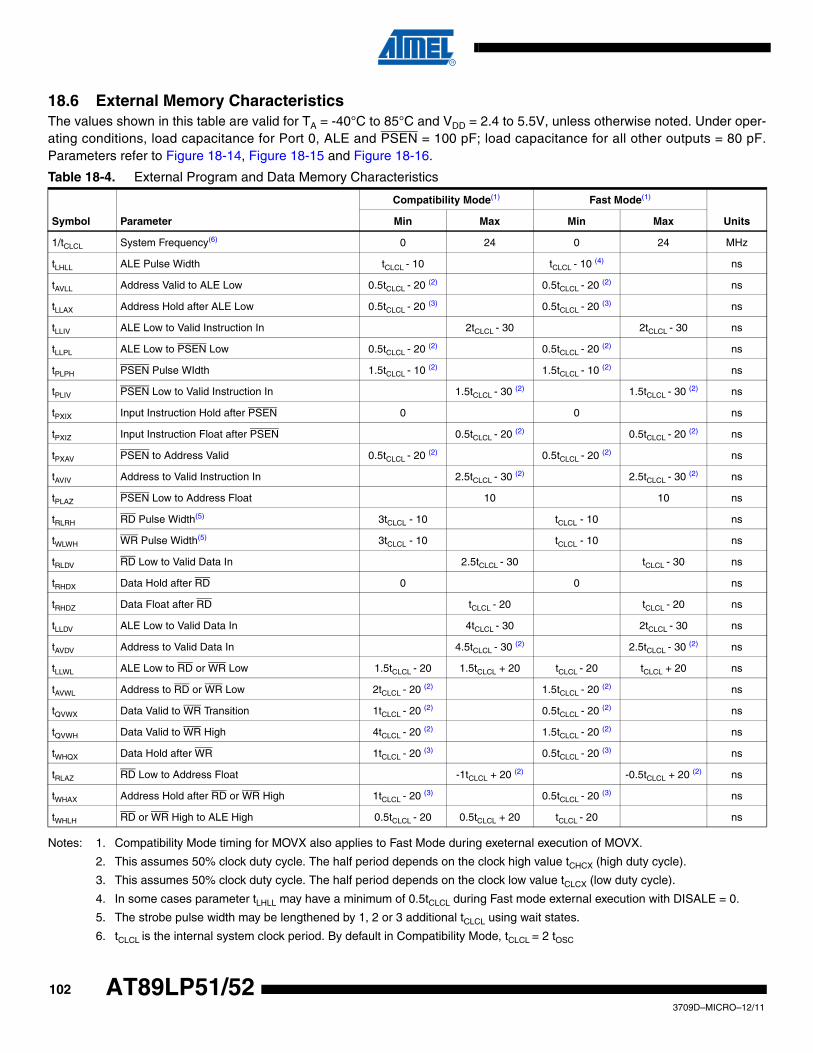
1023709D–MICRO–12/11
AT89LP51/52
18.6 External Memory CharacteristicsThe values shown in this table are valid for TA = -40°C to 85°C and VDD = 2.4 to 5.5V, unless otherwise noted. Under oper-ating conditions, load capacitance for Port 0, ALE and PSEN = 100 pF; load capacitance for all other outputs = 80 pF.Parameters refer to Figure 18-14, Figure 18-15 and Figure 18-16.
Notes: 1. Compatibility Mode timing for MOVX also applies to Fast Mode during exeternal execution of MOVX.
2. This assumes 50% clock duty cycle. The half period depends on the clock high value tCHCX (high duty cycle).
3. This assumes 50% clock duty cycle. The half period depends on the clock low value tCLCX (low duty cycle).
4. In some cases parameter tLHLL may have a minimum of 0.5tCLCL during Fast mode external execution with DISALE = 0.
5. The strobe pulse width may be lengthened by 1, 2 or 3 additional tCLCL using wait states.
6. tCLCL is the internal system clock period. By default in Compatibility Mode, tCLCL = 2 tOSC
Table 18-4. External Program and Data Memory Characteristics
Symbol Parameter
Compatibility Mode(1) Fast Mode(1)
UnitsMin Max Min Max
1/tCLCL System Frequency(6) 0 24 0 24 MHz
tLHLL ALE Pulse Width tCLCL - 10 tCLCL - 10 (4) ns
tAVLL Address Valid to ALE Low 0.5tCLCL - 20 (2) 0.5tCLCL - 20 (2) ns
tLLAX Address Hold after ALE Low 0.5tCLCL - 20 (3) 0.5tCLCL - 20 (3) ns
tLLIV ALE Low to Valid Instruction In 2tCLCL - 30 2tCLCL - 30 ns
tLLPL ALE Low to PSEN Low 0.5tCLCL - 20 (2) 0.5tCLCL - 20 (2) ns
tPLPH PSEN Pulse WIdth 1.5tCLCL - 10 (2) 1.5tCLCL - 10 (2) ns
tPLIV PSEN Low to Valid Instruction In 1.5tCLCL - 30 (2) 1.5tCLCL - 30 (2) ns
tPXIX Input Instruction Hold after PSEN 0 0 ns
tPXIZ Input Instruction Float after PSEN 0.5tCLCL - 20 (2) 0.5tCLCL - 20 (2) ns
tPXAV PSEN to Address Valid 0.5tCLCL - 20 (2) 0.5tCLCL - 20 (2) ns
tAVIV Address to Valid Instruction In 2.5tCLCL - 30 (2) 2.5tCLCL - 30 (2) ns
tPLAZ PSEN Low to Address Float 10 10 ns
tRLRH RD Pulse Width(5) 3tCLCL - 10 tCLCL - 10 ns
tWLWH WR Pulse Width(5) 3tCLCL - 10 tCLCL - 10 ns
tRLDV RD Low to Valid Data In 2.5tCLCL - 30 tCLCL - 30 ns
tRHDX Data Hold after RD 0 0 ns
tRHDZ Data Float after RD tCLCL - 20 tCLCL - 20 ns
tLLDV ALE Low to Valid Data In 4tCLCL - 30 2tCLCL - 30 ns
tAVDV Address to Valid Data In 4.5tCLCL - 30 (2) 2.5tCLCL - 30 (2) ns
tLLWL ALE Low to RD or WR Low 1.5tCLCL - 20 1.5tCLCL + 20 tCLCL - 20 tCLCL + 20 ns
tAVWL Address to RD or WR Low 2tCLCL - 20 (2) 1.5tCLCL - 20 (2) ns
tQVWX Data Valid to WR Transition 1tCLCL - 20 (2) 0.5tCLCL - 20 (2) ns
tQVWH Data Valid to WR High 4tCLCL - 20 (2) 1.5tCLCL - 20 (2) ns
tWHQX Data Hold after WR 1tCLCL - 20 (3) 0.5tCLCL - 20 (3) ns
tRLAZ RD Low to Address Float -1tCLCL + 20 (2) -0.5tCLCL + 20 (2) ns
tWHAX Address Hold after RD or WR High 1tCLCL - 20 (3) 0.5tCLCL - 20 (3) ns
tWHLH RD or WR High to ALE High 0.5tCLCL - 20 0.5tCLCL + 20 tCLCL - 20 ns
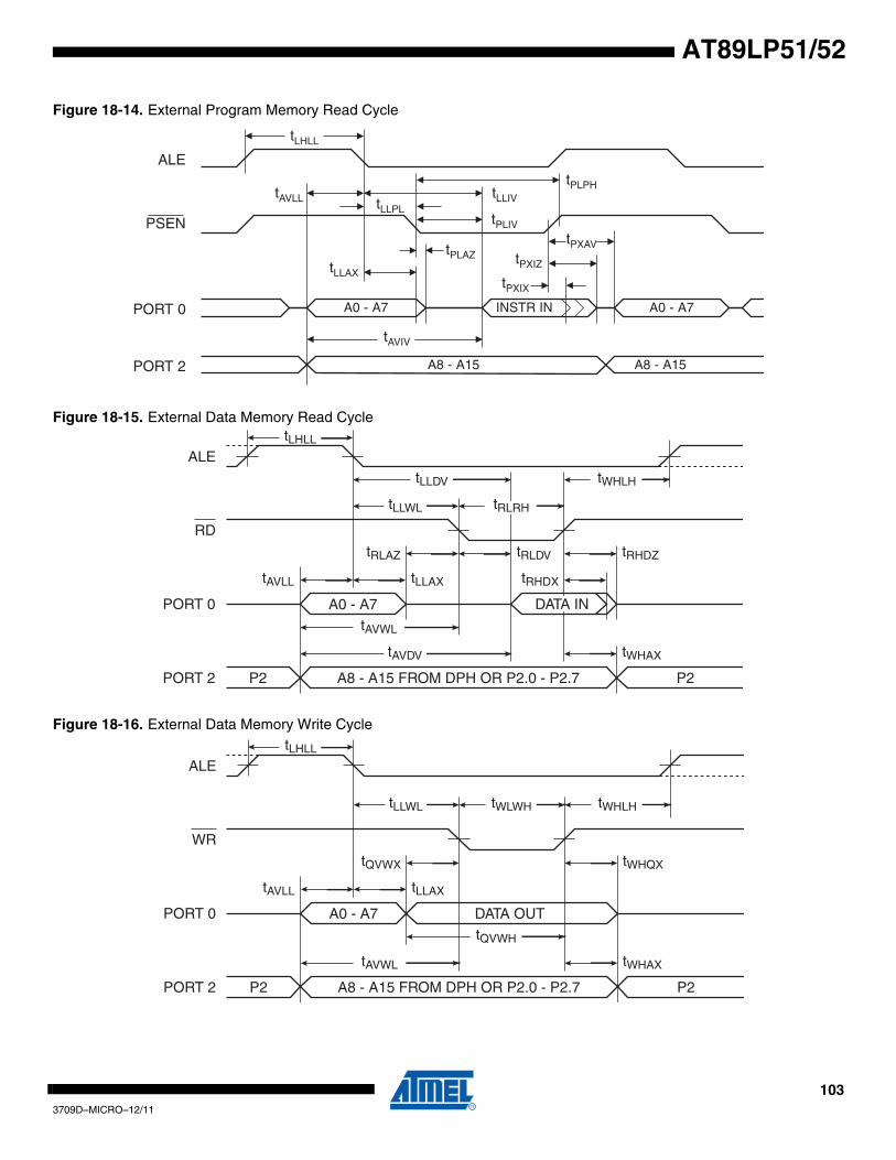
1033709D–MICRO–12/11
AT89LP51/52
Figure 18-14. External Program Memory Read Cycle
Figure 18-15. External Data Memory Read Cycle
Figure 18-16. External Data Memory Write Cycle
tLHLL
tLLIV
tPLIV
tLLAXtPXIZ
tPLPH
tPLAZtPXAV
tAVLL tLLPL
tAVIV
tPXIX
ALE
PSEN
PORT 0
PORT 2 A8 - A15
A0 - A7 A0 - A7
A8 - A15
INSTR IN
tLHLL
ALE
DATA INA0 - A7
A8 - A15 FROM DPH OR P2.0 - P2.7P2 P2
RD
PORT 0
PORT 2
tLLWL tRLRH
tAVLL tLLAX
tRLAZ tRHDZ
tAVWL
tWHLH
tWHAXtAVDV
tLLDV
tRLDV
tRHDX
tLHLL
ALE
DATA OUTA0 - A7
A8 - A15 FROM DPH OR P2.0 - P2.7P2 P2
WR
PORT 0
PORT 2
tLLWL tWLWH
tAVLL tLLAX
tQVWX
tQVWH
tWHQX
tAVWL
tWHLH
tWHAX
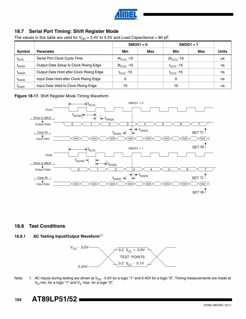
1043709D–MICRO–12/11
AT89LP51/52
Figure 18-17. Shift Register Mode Timing Waveform
18.8 Test Conditions
18.8.1 AC Testing Input/Output Waveform(1)
Note: 1. AC Inputs during testing are driven at VDD - 0.5V for a logic “1” and 0.45V for a logic “0”. Timing measurements are made at VIH min. for a logic “1” and VIL max. for a logic “0”.
18.7 Serial Port Timing: Shift Register ModeThe values in this table are valid for VDD = 2.4V to 5.5V and Load Capacitance = 80 pF.
Symbol Parameter
SMOD1 = 0 SMOD1 = 1
UnitsMin Max Min Max
tXLXL Serial Port Clock Cycle Time 4tCLCL -15 2tCLCL -15 µs
tQVXH Output Data Setup to Clock Rising Edge 3tCLCL -15 tCLCL -15 ns
tXHQX Output Data Hold after Clock Rising Edge tCLCL -15 tCLCL -15 ns
tXHDX Input Data Hold after Clock Rising Edge 0 0 ns
tXHDV Input Data Valid to Clock Rising Edge 15 15 ns
0 1 2 3 4 5 6 7
ValidValidValidValid Valid Valid Valid Valid
Clock
Write to SBUF
Output Data
Clear RI
Input Data
SMOD1 = 0
0 1 2 3 4 5 6 7
ValidValidValidValid Valid Valid Valid Valid
Clock
Write to SBUF
Output Data
Clear RI
Input Data
SMOD1 = 1
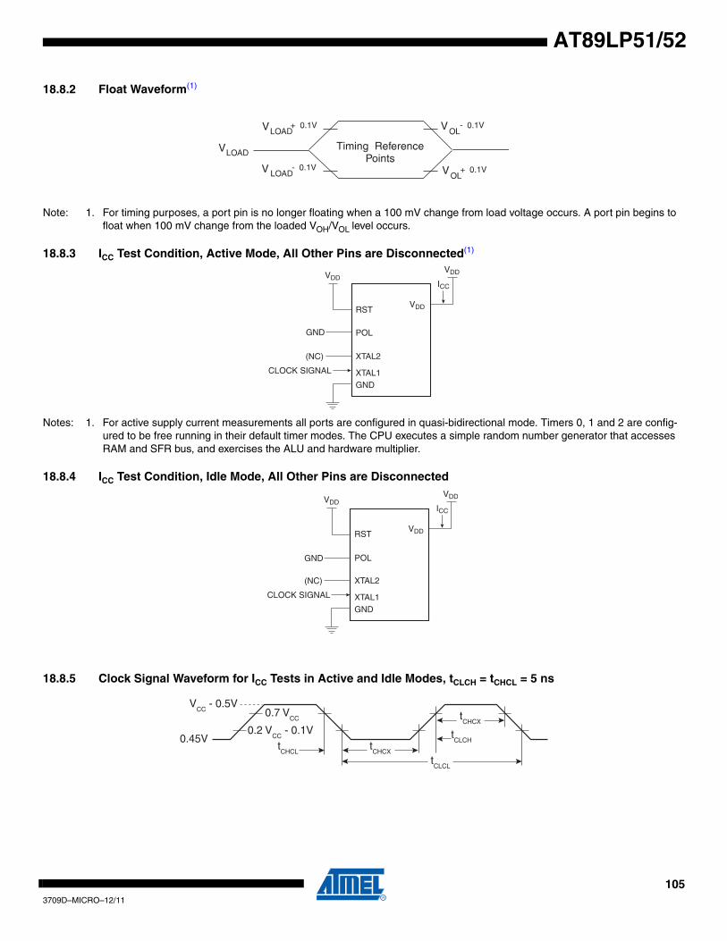
1053709D–MICRO–12/11
AT89LP51/52
18.8.2 Float Waveform(1)
Note: 1. For timing purposes, a port pin is no longer floating when a 100 mV change from load voltage occurs. A port pin begins to float when 100 mV change from the loaded VOH/VOL level occurs.
18.8.3 ICC Test Condition, Active Mode, All Other Pins are Disconnected(1)
Notes: 1. For active supply current measurements all ports are configured in quasi-bidirectional mode. Timers 0, 1 and 2 are config-ured to be free running in their default timer modes. The CPU executes a simple random number generator that accesses RAM and SFR bus, and exercises the ALU and hardware multiplier.
18.8.4 ICC Test Condition, Idle Mode, All Other Pins are Disconnected
18.8.5 Clock Signal Waveform for ICC Tests in Active and Idle Modes, tCLCH = tCHCL = 5 ns
X T AL 2
RST V DD
V DD
I CC
X T AL 1 GND
(NC)
CLOCK SIGNAL
V DD
POLGND
X T AL 2
RSTV DD
V DD
I CC
X T AL 1 GND
(NC)
CLOCK SIGNAL
V DD
GND POL
VCC
- 0.5V
0.45V0.2 V
CC - 0.1V
0.7 VCC
tCHCX
tCHCX
tCLCH
tCHCL
tCLCL
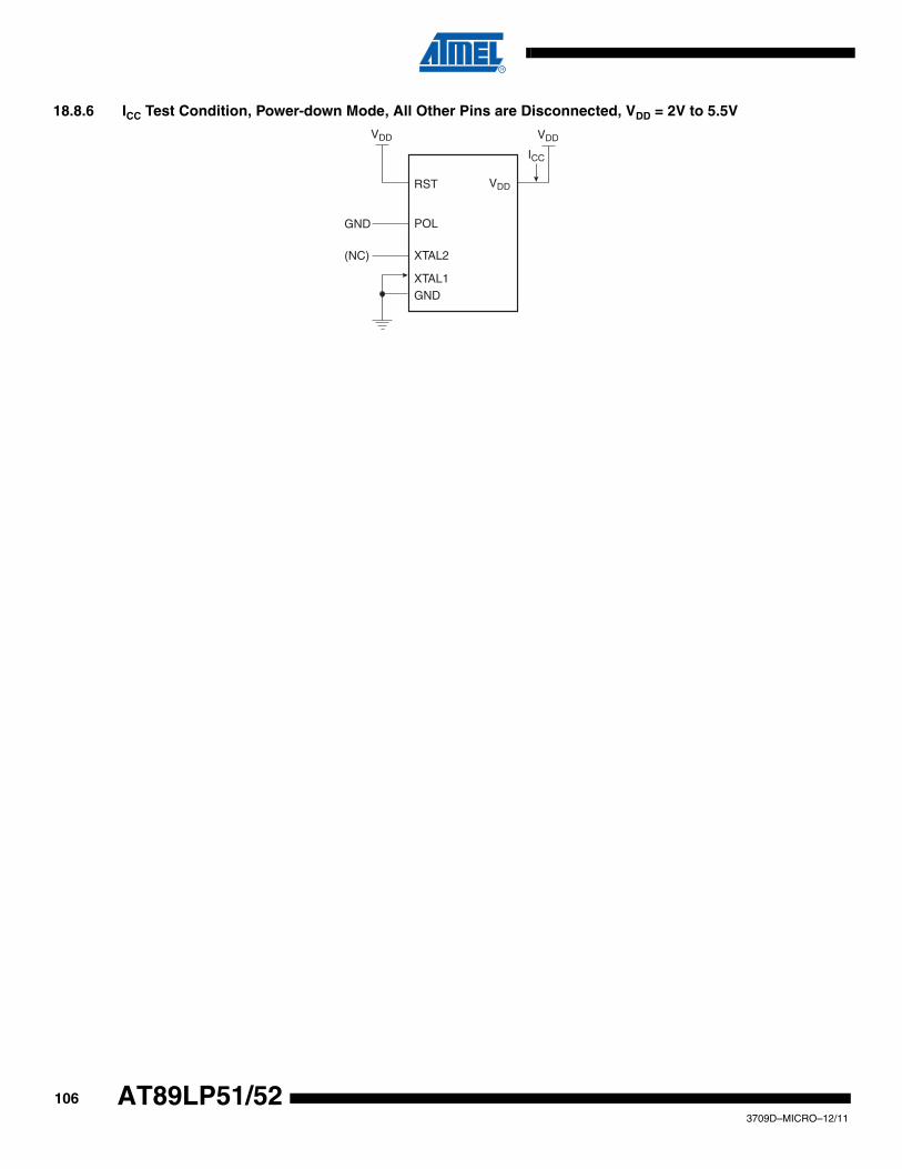
1063709D–MICRO–12/11
AT89LP51/52
18.8.6 ICC Test Condition, Power-down Mode, All Other Pins are Disconnected, VDD = 2V to 5.5V
XTAL2
RST VDD
VDD
ICC
XTAL1 GND
(NC)
VDD
POLGND
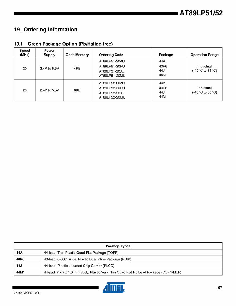
1073709D–MICRO–12/11
AT89LP51/52
19. Ordering Information
19.1 Green Package Option (Pb/Halide-free)Speed (MHz)
PowerSupply Code Memory Ordering Code Package Operation Range
20 2.4V to 5.5V 4KB
AT89LP51-20AU
AT89LP51-20PUAT89LP51-20JUAT89LP51-20MU
44A
40P644J44M1
Industrial(-40° C to 85° C)
20 2.4V to 5.5V 8KB
AT89LP52-20AU
AT89LP52-20PU
AT89LP52-20JUAT89LP52-20MU
44A
40P644J44M1
Industrial(-40° C to 85° C)
Package Types
44A 44-lead, Thin Plastic Quad Flat Package (TQFP)
40P6 40-lead, 0.600” Wide, Plastic Dual Inline Package (PDIP)
44J 44-lead, Plastic J-leaded Chip Carrier (PLCC)
44M1 44-pad, 7 x 7 x 1.0 mm Body, Plastic Very Thin Quad Flat No Lead Package (VQFN/MLF)
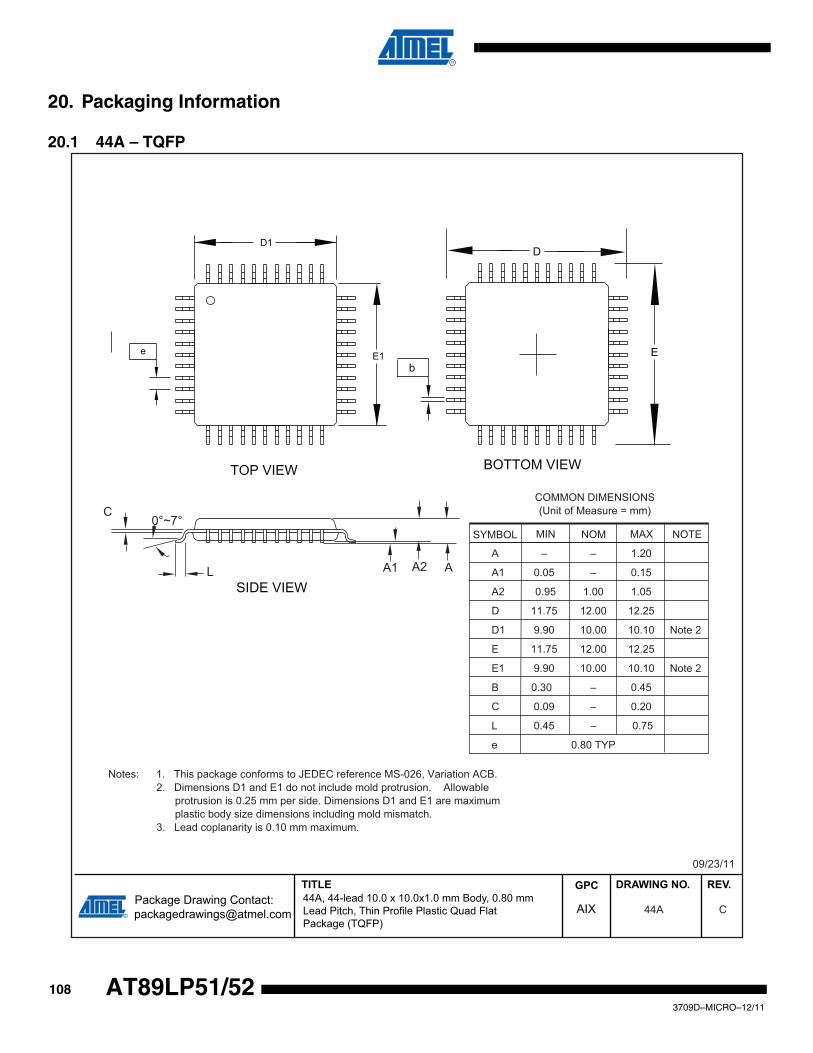
1083709D–MICRO–12/11
AT89LP51/52
20. Packaging Information
20.1 44A – TQFP
Package Drawing Contact:[email protected]
DRAWING NO. REV. TITLE GPC
44A C
09/23/11
44A, 44-lead 10.0 x 10.0x1.0 mm Body, 0.80 mm Lead Pitch, Thin Profile Plastic Quad Flat Package (TQFP)
AIX
0°~7°
L
C
A1 A2 A
D
Eb
BOTTOM VIEW
SIDE VIEW
TOP VIEW
E1
D1
e
COMMON DIMENSIONS(Unit of Measure = mm)
SYMBOL MIN NOM MAX NOTE
Notes: 1. This package conforms to JEDEC reference MS-026, Variation ACB. 2. Dimensions D1 and E1 do not include mold protrusion. Allowable protrusion is 0.25 mm per side. Dimensions D1 and E1 are maximum plastic body size dimensions including mold mismatch. 3. Lead coplanarity is 0.10 mm maximum.
A – – 1.20
A1 0.05 – 0.15
A2 0.95 1.00 1.05
D 11.75 12.00 12.25
D1 9.90 10.00 10.10 Note 2
E 11.75 12.00 12.25
E1 9.90 10.00 10.10 Note 2
B 0.30 – 0.45
C 0.09 – 0.20
L 0.45 – 0.75
e 0.80 TYP
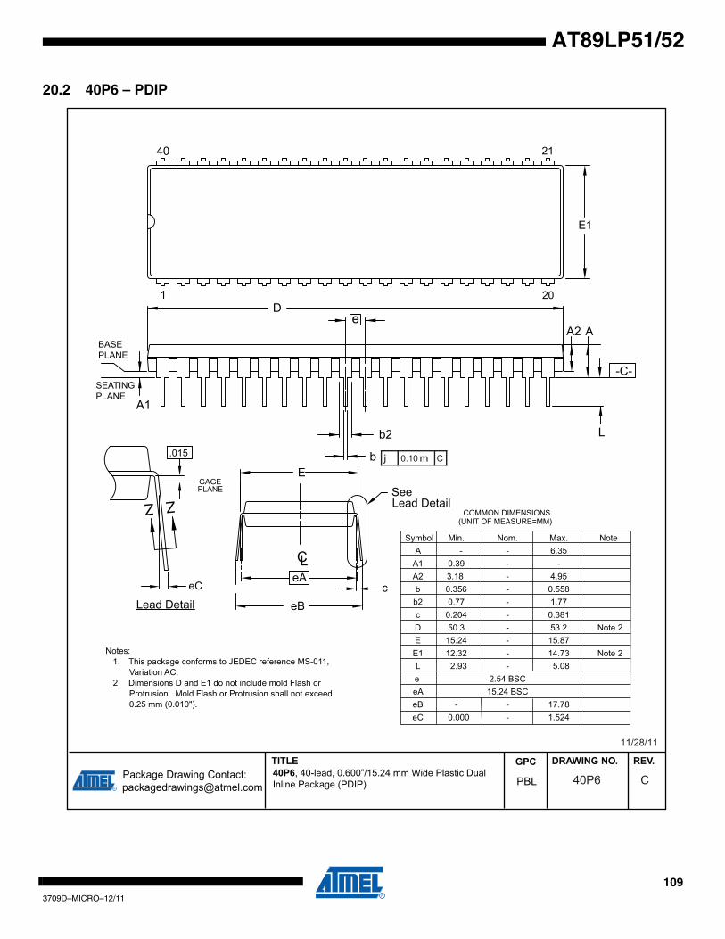
1093709D–MICRO–12/11
AT89LP51/52
20.2 40P6 – PDIP
DRAWING NO. REV. GPCPackage Drawing Contact:[email protected]
TITLE
40P6 C
11/28/11
PBL40P6, 40-lead, 0.600”/15.24 mm Wide Plastic DualInline Package (PDIP)
COMMON DIMENSIONS(UNIT OF MEASURE=MM)
Symbol Min. Nom. Max. Note A - - 6.35 A1 0.39 - - A2 3.18 - 4.95 b 0.356 - 0.558 b2 0.77 - 1.77 c 0.204 - 0.381 D 50.3 - 53.2 Note 2 E 15.24 - 15.87 E1 12.32 - 14.73 Note 2 L 2.93 - 5.08 e 2.54 BSC eA 15.24 BSC eB - - 17.78 eC 0.000 - 1.524
Notes: 1. This package conforms to JEDEC reference MS-011, Variation AC. 2. Dimensions D and E1 do not include mold Flash or Protrusion. Mold Flash or Protrusion shall not exceed 0.25 mm (0.010").
BASEPLANE
SEATING PLANE
40
eC
GAGEPLANE
.015
ZZ
Lead Detail
j 0.10m C
E
ceB
eA
SeeLead Detail
LC
A1
A
L
b
b2
D
A2e
1
21
-C-
E1
20
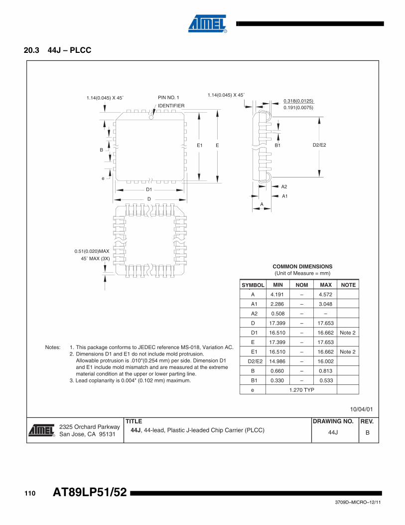
1103709D–MICRO–12/11
AT89LP51/52
20.3 44J – PLCC
Notes: 1. This package conforms to JEDEC reference MS-018, Variation AC. 2. Dimensions D1 and E1 do not include mold protrusion.
Allowable protrusion is .010"(0.254 mm) per side. Dimension D1and E1 include mold mismatch and are measured at the extremematerial condition at the upper or lower parting line.
3. Lead coplanarity is 0.004" (0.102 mm) maximum.
A 4.191 – 4.572
A1 2.286 – 3.048
A2 0.508 – –
D 17.399 – 17.653
D1 16.510 – 16.662 Note 2
E 17.399 – 17.653
E1 16.510 – 16.662 Note 2
D2/E2 14.986 – 16.002
B 0.660 – 0.813
B1 0.330 – 0.533
e 1.270 TYP
COMMON DIMENSIONS(Unit of Measure = mm)
SYMBOL MIN NOM MAX NOTE
1.14(0.045) X 45˚ PIN NO. 1
IDENTIFIER
1.14(0.045) X 45˚
0.51(0.020)MAX
0.318(0.0125)0.191(0.0075)
A2
45˚ MAX (3X)
A
A1
B1 D2/E2B
e
E1 E
D1
D
44J, 44-lead, Plastic J-leaded Chip Carrier (PLCC) B44J
10/04/01
2325 Orchard Parkway San Jose, CA 95131
TITLE DRAWING NO.
R
REV.
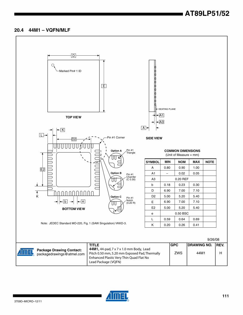
1113709D–MICRO–12/11
AT89LP51/52
20.4 44M1 – VQFN/MLF
TITLE DRAWING NO.GPC REV. Package Drawing Contact: [email protected] 44M1ZWS H
44M1, 44-pad, 7 x 7 x 1.0 mm Body, Lead Pitch 0.50 mm, 5.20 mm Exposed Pad, Thermally Enhanced Plastic Very Thin Quad Flat No Lead Package (VQFN)
9/26/08
COMMON DIMENSIONS(Unit of Measure = mm)
SYMBOL MIN NOM MAX NOTE
A 0.80 0.90 1.00
A1 – 0.02 0.05
A3 0.20 REF
b 0.18 0.23 0.30
D
D2 5.00 5.20 5.40
6.90 7.00 7.10
6.90 7.00 7.10
E
E2 5.00 5.20 5.40
e 0.50 BSC
L 0.59 0.64 0.69
K 0.20 0.26 0.41Note: JEDEC Standard MO-220, Fig. 1 (SAW Singulation) VKKD-3.
TOP VIEW
SIDE VIEW
BOTTOM VIEW
D
E
Marked Pin# 1 ID
E2
D2
b e
Pin #1 CornerL
A1
A3
A
SEATING PLANE
Pin #1 Triangle
Pin #1 Chamfer(C 0.30)
Option A
Option B
Pin #1 Notch(0.20 R)
Option C
K
K
123
1123709D–MICRO–12/11
AT89LP51/52
21. Revision History
Revision No. History
Revision A – September 2010 • Initial Release
Revision B – December 2010• Added AT89LP51 device• Updated Device IDs
• Lowered Minimum Operating Voltage to 2.4V
Revision C – May 2011• Added System Configuration (Section 2.2 on page 7)
• Added Code size to Ordering table
Revision D – December 2011
• Removed Preliminary Status
• Updated AC/DC characteristics (Section 18.2 on page 92 and Section 18.6 on page 102)
• Added typical I/O characteristics (Section 18.3.3 on page 97, Section 18.3.4 on page 98 and Section 18.3.5 on page 99)
• Added note on active power measurement (page 105)
i3709D–MICRO–12/11
AT89LP51/52
Table of Contents
Features ..................................................................................................... 1
1 Pin Configurations ................................................................................... 2
1.1 40-lead PDIP .....................................................................................................2
1.2 44-lead TQFP ....................................................................................................2
.................................................................................................................... 3
1.3 44-lead PLCC ....................................................................................................3
1.4 44-pad VQFN/QFN/MLF ....................................................................................3
1.5 Pin Description ..................................................................................................4
2 Overview ................................................................................................... 6
2.1 Block Diagram ...................................................................................................7
2.2 System Configuration ........................................................................................7
2.3 Comparison to AT89S51/52 ..............................................................................8
3 Memory Organization ............................................................................ 11
3.1 Program Memory .............................................................................................11
3.2 Internal Data Memory ......................................................................................14
3.3 External Data Memory .....................................................................................14
3.4 In-Application Programming (IAP) ...................................................................23
4 Special Function Registers ................................................................... 24
5 Enhanced CPU ....................................................................................... 25
5.1 Fast Mode ........................................................................................................25
5.2 Compatibility Mode ..........................................................................................26
5.3 Enhanced Dual Data Pointers .........................................................................26
6 System Clock ......................................................................................... 29
6.1 Crystal Oscillator .............................................................................................29
6.2 External Clock Source .....................................................................................30
6.3 Internal RC Oscillator ......................................................................................30
6.4 System Clock Divider ......................................................................................31
7 Reset ....................................................................................................... 32
7.1 Power-on Reset ...............................................................................................32
7.2 Brown-out Reset ..............................................................................................33
7.3 External Reset .................................................................................................33
7.4 Watchdog Reset ..............................................................................................34
ii3709D–MICRO–12/11
AT89LP51/52
Table of Contents (Continued)7.5 Software Reset ................................................................................................34
8 Power Saving Modes ............................................................................. 34
8.1 Idle Mode .........................................................................................................34
8.2 Power-down Mode ...........................................................................................35
8.3 Reducing Power Consumption ........................................................................37
9 Interrupts ................................................................................................ 37
9.1 Interrupt Response Time .................................................................................38
10 I/O Ports .................................................................................................. 41
10.1 Port Configuration ............................................................................................41
10.2 Port Read-Modify-Write ...................................................................................44
10.3 Port Alternate Functions ..................................................................................45
11 Timer 0 and Timer 1 ............................................................................... 46
11.1 Mode 0 – 13-bit Timer/Counter ........................................................................47
11.2 Mode 1 – 16-bit Timer/Counter ........................................................................47
11.3 Mode 2 – 8-bit Auto-Reload Timer/Counter .....................................................48
11.4 Mode 3 – 8-bit Split Timer ...............................................................................48
11.5 Clock Output (Pin Toggle Mode) .....................................................................49
12 Timer 2 .................................................................................................... 51
12.1 Timer 2 Registers ............................................................................................52
12.2 Capture Mode ..................................................................................................53
12.3 Auto-Reload Mode ...........................................................................................53
12.4 Baud Rate Generator ......................................................................................55
12.5 Frequency Generator (Programmable Clock Out) ...........................................56
13 External Interrupts ................................................................................. 57
14 Serial Interface (UART) .......................................................................... 57
14.1 Multiprocessor Communications .....................................................................59
14.2 Baud Rates ......................................................................................................59
14.3 Framing Error Detection ..................................................................................61
14.4 Automatic Address Recognition ......................................................................61
14.5 More About Mode 0 .........................................................................................63
14.6 More About Mode 1 .........................................................................................68
14.7 More About Modes 2 and 3 .............................................................................70
iii3709D–MICRO–12/11
AT89LP51/52
Table of Contents (Continued)
15 Programmable Watchdog Timer ........................................................... 73
15.1 Software Reset ................................................................................................73
16 Instruction Set Summary ...................................................................... 75
17 Programming the Flash Memory .......................................................... 79
17.1 Physical Interface ............................................................................................79
17.2 Memory Organization ......................................................................................81
17.3 Command Format ............................................................................................82
17.4 Status Register ................................................................................................85
17.5 DATA Polling ...................................................................................................85
17.6 Flash Security ..................................................................................................85
17.7 User Configuration Fuses ................................................................................86
17.8 User Signature .................................................................................................87
17.9 Programming Interface Timing ........................................................................87
18 Electrical Characteristics ...................................................................... 92
18.1 Absolute Maximum Ratings* ...........................................................................92
18.2 DC Characteristics ...........................................................................................92
18.3 Typical Characteristics ....................................................................................93
18.4 Clock Characteristics .....................................................................................100
18.5 Reset Characteristics ....................................................................................101
18.6 External Memory Characteristics ...................................................................102
18.7 Serial Port Timing: Shift Register Mode ........................................................104
18.8 Test Conditions ..............................................................................................104
19 Ordering Information ........................................................................... 107
19.1 Green Package Option (Pb/Halide-free) ........................................................107
20 Packaging Information ........................................................................ 108
20.1 44A – TQFP ...................................................................................................108
20.2 40P6 – PDIP ..................................................................................................109
20.3 44J – PLCC ...................................................................................................110
20.4 44M1 – VQFN/MLF .......................................................................................111
21 Revision History ................................................................................... 112
Table of Contents....................................................................................... i

iv3709D–MICRO–12/11
AT89LP51/52
3709D–MICRO–12/11
Atmel Corporation2325 Orchard ParkwaySan Jose, CA 95131USATel: (+1) (408) 441-0311Fax: (+1) (408) [email protected]
Atmel Asia LimitedUnit 1-5 & 16, 19/FBEA Tower, Millennium City 5418 Kwun Tong RoadKwun Tong, KowloonHONG KONGTel: (+852) 2245-6100Fax: (+852) 2722-1369
Atmel Munich GmbHBusiness CampusParkring 4D-85748 Garching b. MunichGERMANYTel: (+49) 89-31970-0Fax: (+49) 89-3194621
Atmel Japan9F, Tonetsu Shinkawa Bldg.1-24-8 ShinkawaChuo-ku, Tokyo 104-0033JAPANTel: (+81) (3) 3523-3551Fax: (+81) (3) 3523-7581
Disclaimer: The information in this document is provided in connection with Atmel products. No license, express or implied, by estoppel or otherwise, to anyintellectual property right is granted by this document or in connection with the sale of Atmel products. EXCEPT AS SET FORTH IN ATMEL’S TERMS AND CONDI-TIONS OF SALE LOCATED ON ATMEL’S WEB SITE, ATMEL ASSUMES NO LIABILITY WHATSOEVER AND DISCLAIMS ANY EXPRESS, IMPLIED OR STATUTORYWARRANTY RELATING TO ITS PRODUCTS INCLUDING, BUT NOT LIMITED TO, THE IMPLIED WARRANTY OF MERCHANTABILITY, FITNESS FOR A PARTICULARPURPOSE, OR NON-INFRINGEMENT. IN NO EVENT SHALL ATMEL BE LIABLE FOR ANY DIRECT, INDIRECT, CONSEQUENTIAL, PUNITIVE, SPECIAL OR INCIDEN-TAL DAMAGES (INCLUDING, WITHOUT LIMITATION, DAMAGES FOR LOSS OF PROFITS, BUSINESS INTERRUPTION, OR LOSS OF INFORMATION) ARISING OUT OFTHE USE OR INABILITY TO USE THIS DOCUMENT, EVEN IF ATMEL HAS BEEN ADVISED OF THE POSSIBILITY OF SUCH DAMAGES. Atmel makes norepresentations or warranties with respect to the accuracy or completeness of the contents of this document and reserves the right to make changes to specificationsand product descriptions at any time without notice. Atmel does not make any commitment to update the information contained herein. Unless specifically providedotherwise, Atmel products are not suitable for, and shall not be used in, automotive applications. Atmel’s products are not intended, authorized, or warranted for useas components in applications intended to support or sustain life.
© 2011 Atmel Corporation. All rights reserved. Atmel®, Atmel logo and combinations thereof, and others are registered trademarks or trade-marks of Atmel Corporation or its subsidiaries. Other terms and product names may be trademarks of others.

Mouser Electronics
Authorized Distributor
Click to View Pricing, Inventory, Delivery & Lifecycle Information: Atmel:
AT89LP52-20AU AT89LP52-20MU AT89LP51-20MU AT89LP51-20JU
Related Documents


