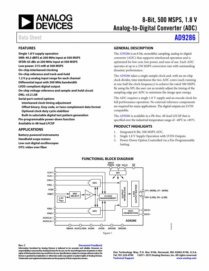
8-Bit, 500 MSPS, 1.8 V Analog-to-Digital Converter (ADC) Data Sheet AD9286 FEATURES Single 1.8 V supply operation SNR: 49.3 dBFS at 200 MHz input at 500 MSPS SFDR: 65 dBc at 200 MHz input at 500 MSPS Low power: 315 mW at 500 MSPS On-chip interleaved clocking On-chip reference and track-and-hold 1.2 V p-p analog input range for each channel Differential input with 500 MHz bandwidth LVDS-compliant digital output On-chip voltage reference and sample-and-hold circuit DNL: ±0.2 LSB Serial port control options Interleaved clock timing adjustment Offset binary, Gray code, or twos complement data format Optional clock duty cycle stabilizer Built-in selectable digital test pattern generation Pin-programmable power-down function Available in 48-lead LFCSP APPLICATIONS Battery-powered instruments Handheld scope meters Low cost digital oscilloscopes OTS: video over fiber GENERAL DESCRIPTION The AD9286 is an 8-bit, monolithic sampling, analog-to-digital converter (ADC) that supports interleaved operation and is optimized for low cost, low power, and ease of use. Each ADC operates at up to a 250 MSPS conversion rate with outstanding dynamic performance. The AD9286 takes a single sample clock and, with an on-chip clock divider, time interleaves the two ADC cores (each running at one-half the clock frequency) to achieve the rated 500 MSPS. By using the SPI, the user can accurately adjust the timing of the sampling edge per ADC to minimize the image spur energy. The ADC requires a single 1.8 V supply and an encode clock for full performance operation. No external reference components are required for many applications. The digital outputs are LVDS compatible. The AD9286 is available in a Pb-free, 48-lead LFCSP that is specified over the industrial temperature range of −40°C to +85°C. PRODUCT HIGHLIGHTS 1. Integrated 8-Bit, 500 MSPS ADC. 2. Single 1.8 V Supply Operation with LVDS Outputs. 3. Power-Down Option Controlled via a Pin-Programmable Setting. FUNCTIONAL BLOCK DIAGRAM AD9286 CLK– VIN1+ VIN1– VREF VCM ADC ADC CLOCK MANAGEMENT CLK+ AUXCLK+ AUXCLK– VIN2– VIN2+ ×1.5 1.0V V REF REF SELECT DCO GENERATION DCO+ DCO– RBIAS AUXCLKEN AGND AVDD DRVDD DRGND SPI SDIO/ PWDN OE SCLK CSB D7+ (MSB), D7– (MSB) D0+ (LSB), D0– (LSB) LVDS OUTPUT BUFFER OUTPUT INTERLEAVE 09338-001 Figure 1. Rev. C Document Feedback Information furnished by Analog Devices is believed to be accurate and reliable. However, no responsibility is assumed by Analog Devices for its use, nor for any infringements of patents or other rights of third parties that may result from its use. Specifications subject to change without notice. No license is granted by implication or otherwise under any patent or patent rights of Analog Devices. Trademarks and registered trademarks are the property of their respective owners. One Technology Way, P.O. Box 9106, Norwood, MA 02062-9106, U.S.A. Tel: 781.329.4700 ©2011–2015 Analog Devices, Inc. All rights reserved. Technical Support www.analog.com

Welcome message from author
This document is posted to help you gain knowledge. Please leave a comment to let me know what you think about it! Share it to your friends and learn new things together.
Transcript
8-Bit, 500 MSPS, 1.8 V Analog-to-Digital Converter (ADC)
Data Sheet AD9286
FEATURES Single 1.8 V supply operation SNR: 49.3 dBFS at 200 MHz input at 500 MSPS SFDR: 65 dBc at 200 MHz input at 500 MSPS Low power: 315 mW at 500 MSPS On-chip interleaved clocking On-chip reference and track-and-hold 1.2 V p-p analog input range for each channel Differential input with 500 MHz bandwidth LVDS-compliant digital output On-chip voltage reference and sample-and-hold circuit DNL: ±0.2 LSB Serial port control options
Interleaved clock timing adjustment Offset binary, Gray code, or twos complement data format Optional clock duty cycle stabilizer Built-in selectable digital test pattern generation
Pin-programmable power-down function Available in 48-lead LFCSP
APPLICATIONS Battery-powered instruments Handheld scope meters Low cost digital oscilloscopes OTS: video over fiber
GENERAL DESCRIPTION The AD9286 is an 8-bit, monolithic sampling, analog-to-digital converter (ADC) that supports interleaved operation and is optimized for low cost, low power, and ease of use. Each ADC operates at up to a 250 MSPS conversion rate with outstanding dynamic performance.
The AD9286 takes a single sample clock and, with an on-chip clock divider, time interleaves the two ADC cores (each running at one-half the clock frequency) to achieve the rated 500 MSPS. By using the SPI, the user can accurately adjust the timing of the sampling edge per ADC to minimize the image spur energy.
The ADC requires a single 1.8 V supply and an encode clock for full performance operation. No external reference components are required for many applications. The digital outputs are LVDS compatible.
The AD9286 is available in a Pb-free, 48-lead LFCSP that is specified over the industrial temperature range of −40°C to +85°C.
PRODUCT HIGHLIGHTS 1. Integrated 8-Bit, 500 MSPS ADC. 2. Single 1.8 V Supply Operation with LVDS Outputs. 3. Power-Down Option Controlled via a Pin-Programmable
Setting.
FUNCTIONAL BLOCK DIAGRAM
AD9286
CLK–
VIN1+
VIN1–
VREF
VCM
ADC
ADC
CLOCKMANAGEMENT
CLK+
AUXCLK+AUXCLK–
VIN2–
VIN2+
×1.51.0VVREF
REFSELECT
DCOGENERATION
DCO+
DCO–
RBIAS AUXCLKEN AGND AVDD DRVDD DRGND
SPI
SDIO/PWDN OESCLKCSB
D7+ (MSB), D7– (MSB)
D0+ (LSB), D0– (LSB)LVD
SO
UTP
UT
BU
FFER
OU
TPU
TIN
TER
LEA
VE
0933
8-00
1
Figure 1.
Rev. C Document Feedback Information furnished by Analog Devices is believed to be accurate and reliable. However, no responsibility is assumed by Analog Devices for its use, nor for any infringements of patents or other rights of third parties that may result from its use. Specifications subject to change without notice. No license is granted by implication or otherwise under any patent or patent rights of Analog Devices. Trademarks and registered trademarks are the property of their respective owners.
One Technology Way, P.O. Box 9106, Norwood, MA 02062-9106, U.S.A. Tel: 781.329.4700 ©2011–2015 Analog Devices, Inc. All rights reserved. Technical Support www.analog.com
AD9286 Data Sheet
TABLE OF CONTENTS Features .............................................................................................. 1 Applications ....................................................................................... 1 General Description ......................................................................... 1 Product Highlights ........................................................................... 1 Functional Block Diagram .............................................................. 1 Revision History ............................................................................... 2 Specifications ..................................................................................... 3
DC Specifications ......................................................................... 3 AC Specifications .......................................................................... 4 Digital Specifications ................................................................... 5 Switching Specifications .............................................................. 6 SPI Timing Specifications ........................................................... 6
Absolute Maximum Ratings ............................................................ 9 Thermal Resistance ...................................................................... 9 ESD Caution .................................................................................. 9
Pin Configuration and Function Descriptions ........................... 10 Typical Performance Characteristics ........................................... 12 Equivalent Circuits ......................................................................... 14 Theory of Operation ...................................................................... 15
ADC Architecture ...................................................................... 15 Analog Input Considerations .................................................... 15
Voltage Reference ....................................................................... 15 RBIAS ........................................................................................... 15 Clock Input Considerations ...................................................... 16 Digital Outputs ........................................................................... 18
Built-In Self-Test (BIST) and Output Test .................................. 19 Built-In Self-Test (BIST) ............................................................ 19 Output Test Modes ..................................................................... 19
Serial Port Interface (SPI) .............................................................. 20 Configuration Using the SPI ..................................................... 20 Hardware Interface ..................................................................... 21 Configuration Without the SPI ................................................ 21 SPI Accessible Features .............................................................. 21
Memory Map .................................................................................. 22 Reading the Memory Map Register Table ............................... 22 Memory Map Register Table ..................................................... 23 Memory Map Register Descriptions ........................................ 25
Applications Information .............................................................. 26 Design Guidelines ...................................................................... 26
Outline Dimensions ....................................................................... 27 Ordering Guide .......................................................................... 27
REVISION HISTORY 1/15—Rev. B to Rev. C Changes to Table 13 ........................................................................ 24 6/13—Rev. A to Rev. B Changes to Clock Input Parameters, Table 4 ................................ 6 Changes to Clocking Modes Section ........................................... 16 Changes to Table 9 .......................................................................... 17 Changes to Register 0x09, Table 13 .............................................. 23 3/11—Rev. 0 to Rev. A Changes to General Description, ADC Conversion Rate ........... 1 1/11—Revision 0: Initial Version
Rev. C | Page 2 of 27
Data Sheet AD9286
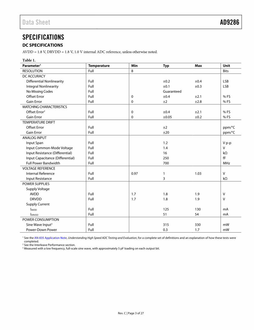
SPECIFICATIONS DC SPECIFICATIONS AVDD = 1.8 V, DRVDD = 1.8 V, 1.0 V internal ADC reference, unless otherwise noted.
Table 1. Parameter1 Temperature Min Typ Max Unit RESOLUTION Full 8 Bits DC ACCURACY
Differential Nonlinearity Full ±0.2 ±0.4 LSB Integral Nonlinearity Full ±0.1 ±0.3 LSB No Missing Codes Full Guaranteed Offset Error Full 0 ±0.4 ±2.1 % FS Gain Error Full 0 ±2 ±2.8 % FS
MATCHING CHARACTERISTICS Offset Error2 Full 0 ±0.4 ±2.1 % FS Gain Error Full 0 ±0.05 ±0.2 % FS
TEMPERATURE DRIFT Offset Error Full ±2 ppm/°C Gain Error Full ±20 ppm/°C
ANALOG INPUT Input Span Full 1.2 V p-p Input Common-Mode Voltage Full 1.4 V Input Resistance (Differential) Full 16 kΩ Input Capacitance (Differential) Full 250 fF Full Power Bandwidth Full 700 MHz
VOLTAGE REFERENCE Internal Reference Full 0.97 1 1.03 V Input Resistance Full 3 kΩ
POWER SUPPLIES Supply Voltage
AVDD Full 1.7 1.8 1.9 V DRVDD Full 1.7 1.8 1.9 V
Supply Current IAVDD Full 125 130 mA IDRVDD Full 51 54 mA
POWER CONSUMPTION Sine Wave Input3 Full 315 330 mW Power-Down Power Full 0.3 1.7 mW
1 See the AN-835 Application Note, Understanding High Speed ADC Testing and Evaluation, for a complete set of definitions and an explanation of how these tests were completed.
2 See the Interleave Performance section. 3 Measured with a low frequency, full-scale sine wave, with approximately 5 pF loading on each output bit.
Rev. C | Page 3 of 27
AD9286 Data Sheet
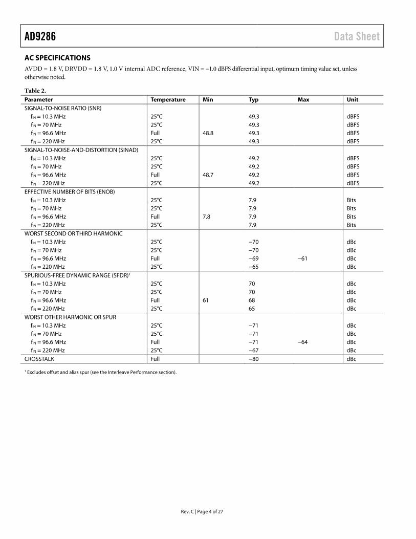
AC SPECIFICATIONS AVDD = 1.8 V, DRVDD = 1.8 V, 1.0 V internal ADC reference, VIN = −1.0 dBFS differential input, optimum timing value set, unless otherwise noted.
Table 2. Parameter Temperature Min Typ Max Unit SIGNAL-TO-NOISE RATIO (SNR)
fIN = 10.3 MHz 25°C 49.3 dBFS fIN = 70 MHz 25°C 49.3 dBFS fIN = 96.6 MHz Full 48.8 49.3 dBFS fIN = 220 MHz 25°C 49.3 dBFS
SIGNAL-TO-NOISE-AND-DISTORTION (SINAD) fIN = 10.3 MHz 25°C 49.2 dBFS fIN = 70 MHz 25°C 49.2 dBFS fIN = 96.6 MHz Full 48.7 49.2 dBFS fIN = 220 MHz 25°C 49.2 dBFS
EFFECTIVE NUMBER OF BITS (ENOB) fIN = 10.3 MHz 25°C 7.9 Bits fIN = 70 MHz 25°C 7.9 Bits fIN = 96.6 MHz Full 7.8 7.9 Bits fIN = 220 MHz 25°C 7.9 Bits
WORST SECOND OR THIRD HARMONIC fIN = 10.3 MHz 25°C −70 dBc fIN = 70 MHz 25°C −70 dBc fIN = 96.6 MHz Full −69 −61 dBc fIN = 220 MHz 25°C −65 dBc
SPURIOUS-FREE DYNAMIC RANGE (SFDR)1 fIN = 10.3 MHz 25°C 70 dBc fIN = 70 MHz 25°C 70 dBc fIN = 96.6 MHz Full 61 68 dBc fIN = 220 MHz 25°C 65 dBc
WORST OTHER HARMONIC OR SPUR fIN = 10.3 MHz 25°C −71 dBc fIN = 70 MHz 25°C −71 dBc fIN = 96.6 MHz Full −71 −64 dBc fIN = 220 MHz 25°C −67 dBc
CROSSTALK Full −80 dBc
1 Excludes offset and alias spur (see the Interleave Performance section).
Rev. C | Page 4 of 27
Data Sheet AD9286
DIGITAL SPECIFICATIONS AVDD = 1.8 V, DRVDD = 1.8 V, 1.0 V internal ADC reference, AIN = 5 MHz, full temperature, unless otherwise noted.
Table 3. Parameter1 Temperature Min Typ Max Unit CLOCK INPUTS (CLK+, CLK−, AUXCLK+, AUXCLK−)
Logic Compliance LVDS/PECL Internal Common-Mode Bias Full 1.2 V Differential Input Voltage2 Full 0.2 6 V p-p Input Voltage Range Full AVDD − 0.3 AVDD + 1.6 V High Level Input Voltage Full 1.2 3.6 V Low Level Input Voltage Full 0 0.8 V High Level Input Current Full −10 +10 µA Low Level Input Current Full −10 +10 µA Input Resistance (Differential) 25°C 20 kΩ Input Capacitance 25°C 4 pF
LOGIC INPUTS CSB
High Level Input Voltage Full 1.2 DRVDD + 0.3 V Low Level Input Voltage Full 0 0.8 V High Level Input Current Full −5 −0.4 +5 µA Low Level Input Current Full −80 −63 −50 µA Input Resistance 25°C 30 kΩ Input Capacitance 25°C 2 pF
SCLK, SDIO/PWDN, AUXCLKEN, OE
High Level Input Voltage Full 1.2 DRVDD + 0.3 V Low Level Input Voltage Full 0 0.8 V High Level Input Current Full 50 57 70 µA Low Level Input Current Full −5 −0.4 +5 µA Input Resistance 25°C 30 kΩ Input Capacitance 25°C 2 pF
DIGITAL OUTPUTS (D7+, D7− to D0+, D0−), LVDS DRVDD = 1.8 V
Differential Output Voltage (VOD) Full 290 345 400 mV Output Offset Voltage (VOS) Full 1.15 1.25 1.35 V Output Coding (Default) Offset binary
1 See the AN-835 Application Note, Understanding High Speed ADC Testing and Evaluation, for a complete set of definitions and an explanation of how these tests were completed.
2 Specified for LVDS and LVPECL only.
Rev. C | Page 5 of 27
AD9286 Data Sheet
Rev. C | Page 6 of 27
SWITCHING SPECIFICATIONS AVDD = 1.8 V, DRVDD = 1.8 V, maximum sample rate, −1.0 dBFS differential input, 1.0 V internal reference, unless otherwise noted.
Table 4. Parameter Temperature Min Typ Max Unit CLOCK INPUT PARAMETERS
Input Clock Rate Full 60 500 MHz CLK Period (tCLK) Full 2 Ns CLK Pulse Width High (tCH) Full 1 Ns
DATA OUTPUT PARAMETERS Data Propagation Delay (tPD) 3.7 ns DCO Propagation Delay (tDCO) Full 3.7 ns DCO to Data Skew (tSKEW) Full −280 −60 100 ps Pipeline Delay (Latency) Full 11 Cycles Aperture Delay (tA) Full 1.0 ns Aperture Uncertainty (Jitter, tJ) Full 0.1 ps rms Wake-Up Time1 Full 500 μs
OUT-OF-RANGE RECOVERY TIME Full 4 Cycles 1 Wake-up time is dependent on the value of the decoupling capacitors.
SPI TIMING SPECIFICATIONS
Table 5. Parameter Description Min Typ Max Unit SPI TIMING REQUIREMENTS
tDS Setup time between the data and the rising edge of SCLK 2 ns tDH Hold time between the data and the rising edge of SCLK 2 ns tCLK Period of the SCLK 40 ns tS Setup time between CSB and SCLK 2 ns tH Hold time between CSB and SCLK 2 ns tHIGH SCLK pulse width high 10 ns tLOW SCLK pulse width low 10 ns tEN_SDIO Time required for the SDIO pin to switch from an input
to an output relative to the SCLK falling edge 10 ns
tDIS_SDIO Time required for the SDIO pin to switch from an output to an input relative to the SCLK rising edge
10 ns
Timing Diagrams
0933
8-00
2
N – 1N – 2
N + 1
M – 11 N – 11 M – 10 N – 10 M – 9 N – 9 M – 8 M – 7N – 8
N + 2
N + 4N + 3
N
tCHtCLK
M + 5M + 4
M + 3
M + 1 M + 2
tA
M
M – 1
VIN1+, VIN1–
VIN2+, VIN2–
CLK+
CLK–
DCO+, DCO–
DATA
tA
tDCO
tSKEW
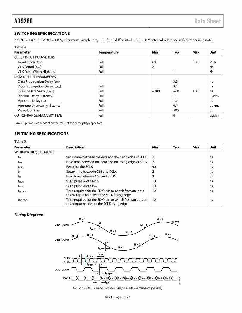
tPD Figure 2. Output Timing Diagram, Sample Mode = Interleaved (Default)
Data Sheet AD9286
Rev. C | Page 7 of 27
0933
8-00
5
N – 1
N + 1
N – 11 M – 10 N – 10 M – 9 N – 9 M – 8 M – 7N – 8 N – 7
N + 2
N + 4N + 5
N + 3
M + 5M + 4
M + 3
M + 1 M + 2
M
N
M – 1
VIN1+, VIN1–
VIN2+, VIN2–
CLK+
CLK–
DCO+, DCO–
DATA
tA
tCH tCLK
tDCO
tSKEW
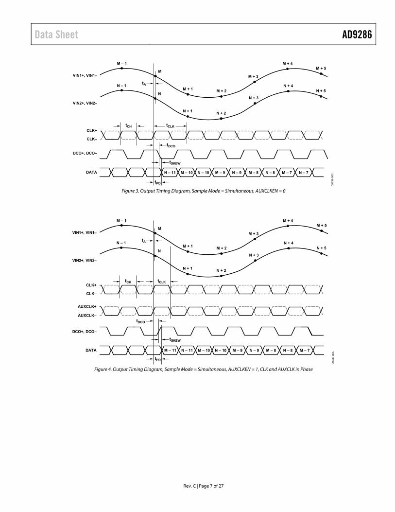
tPD Figure 3. Output Timing Diagram, Sample Mode = Simultaneous, AUXCLKEN = 0
0933
8-00
6N – 11M – 11 M – 10 N – 10 M – 9 N – 9 M – 8 M – 7N – 8
CLK+
CLK–
DCO+, DCO–
DATA
AUXCLK+
AUXCLK–
N – 1
N + 1 N + 2
N + 4N + 5
N + 3
M + 5M + 4
M + 3
M + 1 M + 2
M
N
M – 1
VIN1+, VIN1–
VIN2+, VIN2–
tA
tCH tCLK
tDCO
tSKEW
tPD
Figure 4. Output Timing Diagram, Sample Mode = Simultaneous, AUXCLKEN = 1, CLK and AUXCLK in Phase
AD9286 Data Sheet
Rev. C | Page 8 of 27
0933
8-00
7
CLK+
CLK–
DCO+, DCO–
DATA
AUXCLK+
AUXCLK–
N – 1N – 2
N + 1
N + 2
N + 4N + 3
N
VIN1+, VIN1–
VIN2+, VIN2–
tA
M – 1
M + 1
M + 5M + 4
M + 3
M + 2
M
tA
tCH tCLK
tDCO
tSKEW
tPD
N – 11M – 11 M – 10 N – 10 M – 9 N – 9 M – 8 M – 7N – 8
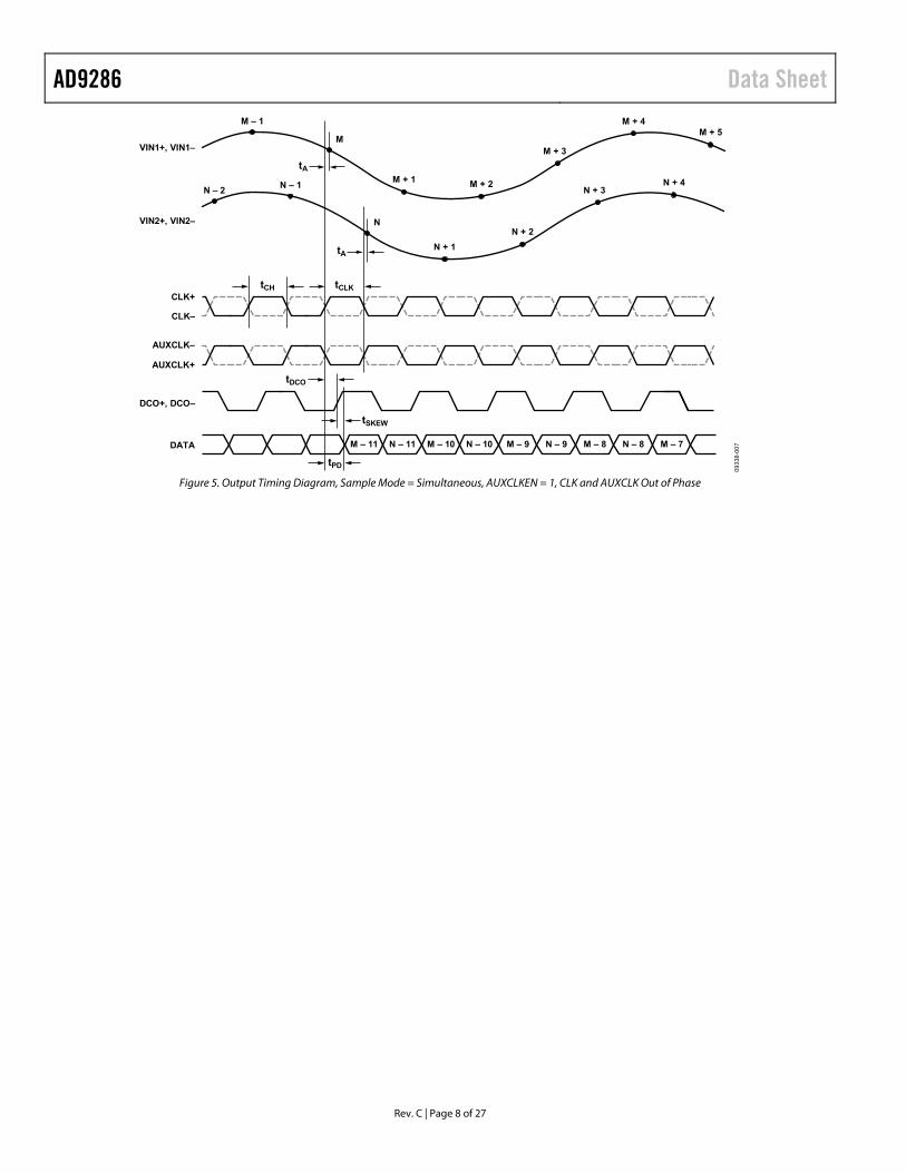
Figure 5. Output Timing Diagram, Sample Mode = Simultaneous, AUXCLKEN = 1, CLK and AUXCLK Out of Phase
Data Sheet AD9286
ABSOLUTE MAXIMUM RATINGS Table 6. Parameter Rating Electrical
AVDD to AGND −0.3 V to +2.0 V DRVDD to DRGND −0.3 V to +2.0 V AGND to DRGND −0.3 V to +0.3 V AVDD to DRVDD −2.0 V to +2.0 V D0+/D0− through D7+/D7−
to DRGND −0.3 V to DRVDD + 0.3 V
DCO+, DCO− to DRGND −0.3 V to DRVDD + 0.3 V CLK+, CLK− to AGND −0.3 V to AVDD + 0.2 V AUXCLK+, AUXCLK− to AGND −0.3 V to AVDD + 0.2 V VIN1±, VIN2± to AGND −0.3 V to AVDD + 0.2 V SDIO/PWDN to DRGND −0.3 V to DRVDD + 0.3 V CSB to AGND −0.3 V to DRVDD + 0.3 V SCLK to AGND −0.3 V to DRVDD + 0.3 V
Environmental Storage Temperature Range −65°C to +125°C Operating Temperature Range −40°C to +85°C Lead Temperature
(Soldering, 10 sec) 300°C
Junction Temperature 150°C
Stresses at or above those listed under Absolute Maximum Ratings may cause permanent damage to the product. This is a stress rating only; functional operation of the product at these or any other conditions above those indicated in the operational section of this specification is not implied. Operation beyond the maximum operating conditions for extended periods may affect product reliability.
THERMAL RESISTANCE θJA is specified for the worst-case conditions, that is, a device soldered in a circuit board for surface-mount packages.
Table 7. Thermal Resistance Package Type θJA θJC Unit 48-Lead LFCSP (CP-48-12) 30.4 2.9 °C/W
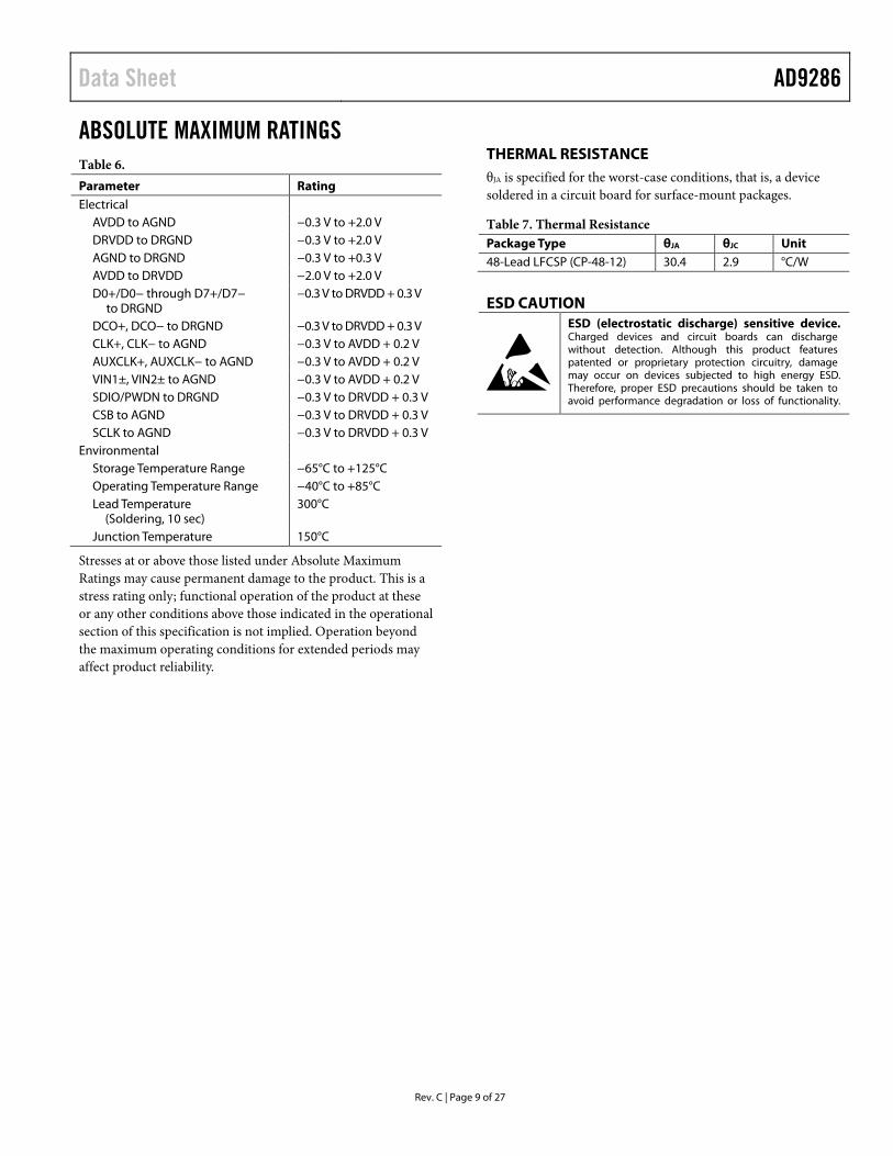
ESD CAUTION
Rev. C | Page 9 of 27
AD9286 Data Sheet
Rev. C | Page 10 of 27
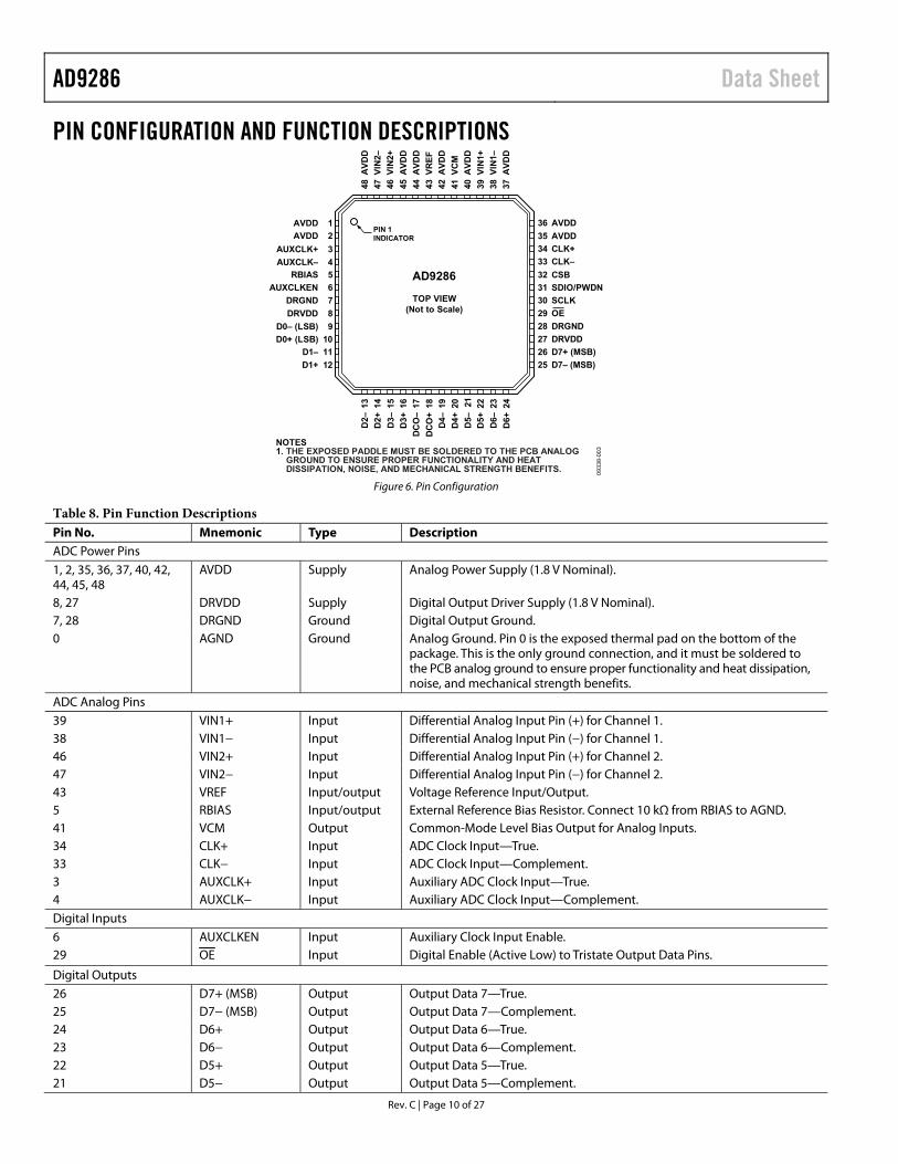
PIN CONFIGURATION AND FUNCTION DESCRIPTIONS
0933
8-00
3
13 14 15 16 17 18 19 20 21 22 23 24
D2–
D2+
D3–
D3+
DC
O–
DC
O+
D4–
D4+
D5–
D5+
D6–
D6+
48 47 46 45 44 43 42 41 40 39 38 37
AV
DD
VIN
2–
VIN
2+
AV
DD
AV
DD
VR
EF
AV
DD
VC
M
AV
DD
VIN
1+
VIN
1–
AV
DD
1
2
3
4
5
6
7
8
9
10
11
12
AVDD
AVDD
AUXCLK+
AUXCLK–
RBIAS
AUXCLKEN
DRGND
DRVDD
D0– (LSB)
D0+ (LSB)
D1–
D1+
AVDD
CLK+
CLK–
CSB
SDIO/PWDN
SCLK
OE
DRGND
DRVDD
D7+ (MSB)
D7– (MSB)
35
AVDD36
34
33
32
31
30
29
28
27
26
25
AD9286
TOP VIEW(Not to Scale)
PIN 1INDICATOR
NOTES1. THE EXPOSED PADDLE MUST BE SOLDERED TO THE PCB ANALOG
GROUND TO ENSURE PROPER FUNCTIONALITY AND HEATDISSIPATION, NOISE, AND MECHANICAL STRENGTH BENEFITS.
Figure 6. Pin Configuration
Table 8. Pin Function Descriptions Pin No. Mnemonic Type Description ADC Power Pins 1, 2, 35, 36, 37, 40, 42, 44, 45, 48
AVDD Supply Analog Power Supply (1.8 V Nominal).
8, 27 DRVDD Supply Digital Output Driver Supply (1.8 V Nominal). 7, 28 DRGND Ground Digital Output Ground. 0 AGND Ground Analog Ground. Pin 0 is the exposed thermal pad on the bottom of the
package. This is the only ground connection, and it must be soldered to the PCB analog ground to ensure proper functionality and heat dissipation, noise, and mechanical strength benefits.
ADC Analog Pins 39 VIN1+ Input Differential Analog Input Pin (+) for Channel 1. 38 VIN1− Input Differential Analog Input Pin (−) for Channel 1. 46 VIN2+ Input Differential Analog Input Pin (+) for Channel 2. 47 VIN2− Input Differential Analog Input Pin (−) for Channel 2. 43 VREF Input/output Voltage Reference Input/Output. 5 RBIAS Input/output External Reference Bias Resistor. Connect 10 kΩ from RBIAS to AGND. 41 VCM Output Common-Mode Level Bias Output for Analog Inputs. 34 CLK+ Input ADC Clock Input—True. 33 CLK− Input ADC Clock Input—Complement. 3 AUXCLK+ Input Auxiliary ADC Clock Input—True. 4 AUXCLK− Input Auxiliary ADC Clock Input—Complement. Digital Inputs 6 AUXCLKEN Input Auxiliary Clock Input Enable. 29 OE Input Digital Enable (Active Low) to Tristate Output Data Pins.
Digital Outputs 26 D7+ (MSB) Output Output Data 7—True. 25 D7− (MSB) Output Output Data 7—Complement. 24 D6+ Output Output Data 6—True. 23 D6− Output Output Data 6—Complement. 22 D5+ Output Output Data 5—True. 21 D5− Output Output Data 5—Complement.
Data Sheet AD9286
Pin No. Mnemonic Type Description 20 D4+ Output Output Data 4—True. 19 D4− Output Output Data 4—Complement. 16 D3+ Output Output Data 3—True. 15 D3− Output Output Data 3—Complement. 14 D2+ Output Output Data 2—True. 13 D2− Output Output Data 2—Complement. 12 D1+ Output Output Data 1—True. 11 D1− Output Output Data 1—Complement. 10 D0+ (LSB) Output Output Data 0—True. 9 D0− (LSB) Output Output Data 0—Complement. 18 DCO+ Output Data Clock Output—True. 17 DCO− Output Data Clock Output—Complement. SPI Control Pins 30 SCLK Input SPI Serial Clock. 31 SDIO/PWDN Input/output SPI Serial Data I/O (SDIO)/Power-Down Input in External Mode (PWDN). 32 CSB Input SPI Chip Select (Active Low).
Rev. C | Page 11 of 27
AD9286 Data Sheet
Rev. C | Page 12 of 27
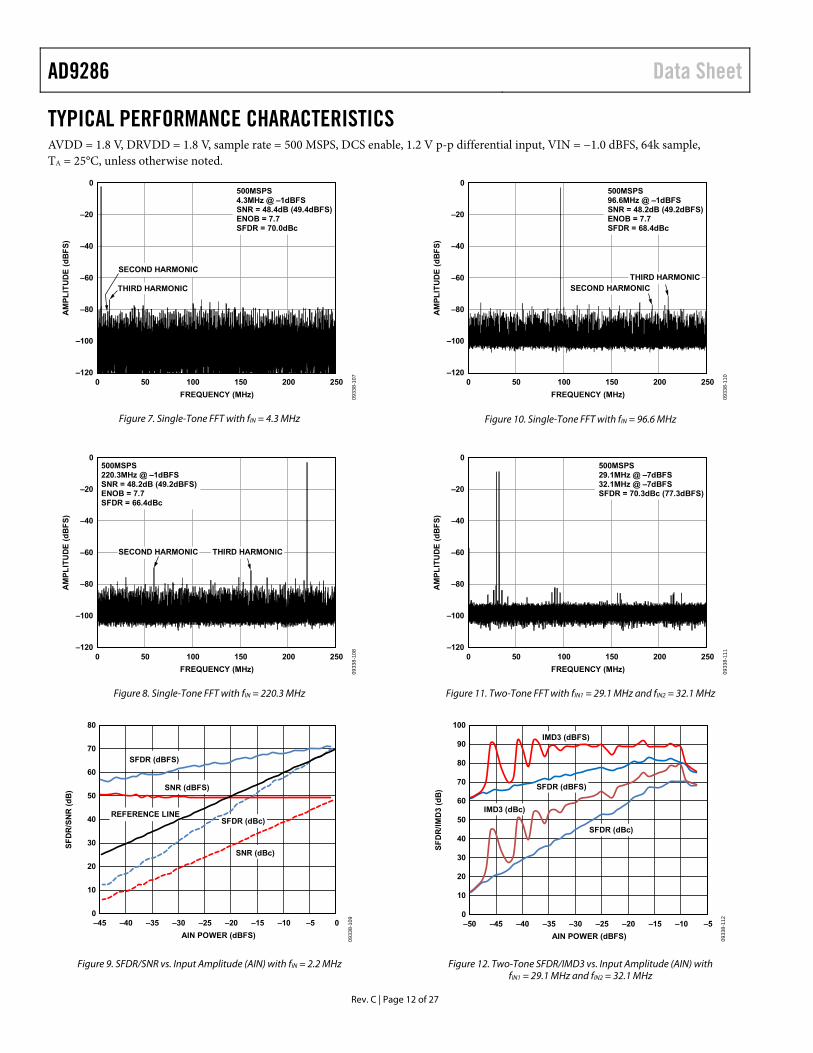
TYPICAL PERFORMANCE CHARACTERISTICSAVDD = 1.8 V, DRVDD = 1.8 V, sample rate = 500 MSPS, DCS enable, 1.2 V p-p differential input, VIN = −1.0 dBFS, 64k sample, TA = 25°C, unless otherwise noted.
0
–20
–40
–60
–80
–100
–1200 50 100 150 200 250
AM
PL
ITU
DE
(d
BF
S)
FREQUENCY (MHz)
500MSPS4.3MHz @ –1dBFSSNR = 48.4dB (49.4dBFS)ENOB = 7.7SFDR = 70.0dBc
SECOND HARMONIC
THIRD HARMONIC
0933
8-10
7
Figure 7. Single-Tone FFT with fIN = 4.3 MHz
0
–20
–40
–60
–80
–100
–1200 50 100 150 200 250
AM
PL
ITU
DE
(d
BF
S)
FREQUENCY (MHz)
500MSPS220.3MHz @ –1dBFSSNR = 48.2dB (49.2dBFS)ENOB = 7.7SFDR = 66.4dBc
SECOND HARMONIC THIRD HARMONIC
0933
8-10
8
Figure 8. Single-Tone FFT with fIN = 220.3 MHz
80
60
70
50
40
30
20
10
0–45 0–5–10–15–20–25–30–35–40
SF
DR
/SN
R (
dB
)
AIN POWER (dBFS)
SFDR (dBFS)
SNR (dBFS)
SFDR (dBc)
SNR (dBc)
REFERENCE LINE
0933
8-10
9
Figure 9. SFDR/SNR vs. Input Amplitude (AIN) with fIN = 2.2 MHz
0
–20
–40
–60
–80
–100
–1200 50 100 150 200 250
AM
PL
ITU
DE
(d
BF
S)
FREQUENCY (MHz)
500MSPS96.6MHz @ –1dBFSSNR = 48.2dB (49.2dBFS)ENOB = 7.7SFDR = 68.4dBc
SECOND HARMONICTHIRD HARMONIC
0933
8-11
0
Figure 10. Single-Tone FFT with fIN = 96.6 MHz
0
–20
–40
–60
–80
–100
–1200 50 100 150 200 250
AM
PL
ITU
DE
(d
BF
S)
FREQUENCY (MHz)
500MSPS29.1MHz @ –7dBFS32.1MHz @ –7dBFSSFDR = 70.3dBc (77.3dBFS)
0933
8-11
1
Figure 11. Two-Tone FFT with fIN1 = 29.1 MHz and fIN2 = 32.1 MHz
100
0
10
20
30
40
50
60
70
80
90
–50 –5–10–15–20–25–30–35–40–45
SF
DR
/IM
D3
(dB
)
AIN POWER (dBFS)
IMD3 (dBFS)
SFDR (dBFS)
SFDR (dBc)
IMD3 (dBc)
0933
8-11
2
Figure 12. Two-Tone SFDR/IMD3 vs. Input Amplitude (AIN) with fIN1 = 29.1 MHz and fIN2 = 32.1 MHz
Data Sheet AD9286
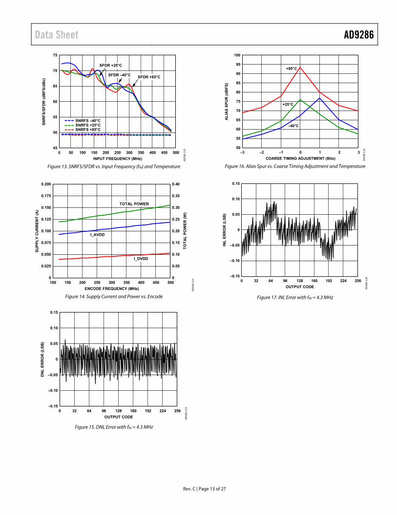
Rev. C | Page 13 of 27
75
70
65
60
55
50
450 50 100 150 200 250 300 350 400 450 500
SN
RF
S/S
FD
R (
dB
FS
/dB
c)
INPUT FREQUENCY (MHz)
SFDR +85°CSFDR –40°C
SFDR +25°C
SNRFS –40°CSNRFS +25°CSNRFS +85°C
0933
8-11
3
Figure 13. SNRFS/SFDR vs. Input Frequency (fIN) and Temperature
0.200
0.175
0.150
0.125
0.100
0.075
0.050
0.025
0
0.40
0.35
0.30
0.25
0.20
0.15
0.10
0.05
0100 150 200 250 300 350 400 450 500
SU
PP
LY
CU
RR
EN
T (
A)
TO
TA
L P
OW
ER
(W
)
ENCODE FREQUENCY (MHz)
TOTAL POWER
I_AVDD
I_DVDD
0933
8-11
4
Figure 14. Supply Current and Power vs. Encode
0.15
0.10
0.05
0
–0.05
–0.10
–0.150 32 64 96 128 160 192 224 256
DN
L E
RR
OR
(L
SB
)
OUTPUT CODE 0933
8-11
5
Figure 15. DNL Error with fIN = 4.3 MHz
100
95
90
85
80
75
70
65
60
55
50–3 –2 –1 0 1 2 3
AL
IAS
SP
UR
(d
BF
S)
COARSE TIMING ADJUSTMENT (Bits) 0933
8-11
6
+85°C
–40°C
+25°C
Figure 16. Alias Spur vs. Coarse Timing Adjustment and Temperature
0.15
0.10
0.05
0
–0.05
–0.10
–0.150 32 64 96 128 160 192 224 256
INL
ER
RO
R (
LS
B)
OUTPUT CODE 0933
8-11
8
Figure 17. INL Error with fIN = 4.3 MHz
AD9286 Data Sheet
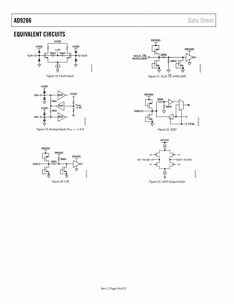
EQUIVALENT CIRCUITS
AVDD1.2V
AVDD
CLK+
AVDD
CLK–10kΩ 10kΩ
0933
8-01
9
Figure 18. Clock Inputs
AVDD
VIN+ BUF
AVDD
VIN– BUF
BUF
AVDD
VCML~1.4V
8kΩ
8kΩ
0933
8-02
0
Figure 19. Analog Inputs (VCML = ~1.4 V)
DRVDD
DRVDD
DRVDD
CSB350Ω
30kΩ
0933
8-02
1
Figure 20. CSB
DRVDD
DRVDD
350Ω
30kΩ
0933
8-02
2
SCLK, OE,AUXCLKEN
Figure 21. SCLK, OE, AUXCLKEN
DRVDD
SDIO
CTRL
350Ω
0933
8-02
3
30kΩ
Figure 22. SDIO
DRVDD
D7– TO D0– D7+ TO D0+
V+
V–
V–
V+
0933
8-02
4
Figure 23. LVDS Output Driver
Rev. C | Page 14 of 27
Data Sheet AD9286
Rev. C | Page 15 of 27
THEORY OF OPERATION The AD9286 is a pipeline-type converter. The input buffers are differential, and both sets of inputs are internally biased. This allows the use of ac or dc input modes. A sample-and-hold amplifier is incorporated into the first stage of the multistage pipeline converter core. The output staging block aligns the data, carries out error correction for the pipeline stages, and feeds that data to the output interleave block and, finally, to the output buffers. All user-selected options are programmed through dedicated digital input pins or a serial port interface (SPI).
ADC ARCHITECTURE Each interleaving channel of the AD9286 consists of a differential input buffer followed by a sample-and-hold amplifier (SHA). This SHA is followed by a pipeline switched-capacitor ADC. The quantized outputs from each stage are combined into a final 8-bit result in the digital correction logic. The pipelined archi-tecture permits the first stage to operate on a new input sample, whereas the remaining stages operate on preceding samples.
Each stage of the pipeline, excluding the last, consists of a low resolution flash ADC connected to a switched-capacitor DAC and interstage residue amplifier (MDAC). The residue amplifier magnifies the difference between the reconstructed DAC output and the flash input for the next stage in the pipeline. One bit of redundancy is used in each stage to facilitate digital correction of flash errors. The last stage consists of a flash ADC.
The input stage contains a differential SHA that can be ac- or dc-coupled in differential or single-ended mode. The output staging block aligns the data, carries out the error correction, and passes the data to the output buffers. The output buffers are powered from a separate supply, allowing adjustment of the output voltage swing. During power-down, the output buffers go into a high impedance state.
The outputs from both interleaving channels are time interleaved to achieve an effective 500 MSPS.
ANALOG INPUT CONSIDERATIONS The analog inputs of the AD9286 are differentially buffered. For best dynamic performance, the source impedances driving VIN1+, VIN1−, VIN2+, and VIN2− should be matched such that common-mode settling errors are symmetrical. Because the AD9286 interleaves two ADC cores, special attention should be given, during board layout, to the symmetry of the two analog paths. Mismatch introduces undesired distortion. The analog inputs are optimized to provide superior wideband performance and must be driven differentially. SNR and SINAD performance degrades significantly if the analog inputs are driven with a single-ended signal.
A wideband transformer, such as Mini-Circuits® ADT1-1WT, can provide the differential analog inputs for applications that require a single-ended-to-differential conversion. Both analog inputs are self-biased by an on-chip resistor divider to a nominal 1.4 V.
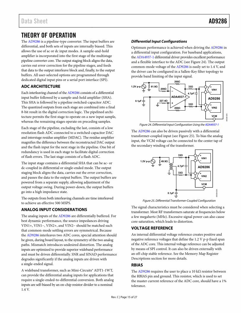
Differential Input Configurations
Optimum performance is achieved when driving the AD9286 in a differential input configuration. For baseband applications, the ADA4937-1 differential driver provides excellent performance and a flexible interface to the ADC (see Figure 24). The output common-mode voltage of the AD9286 is easily set to 1.4 V, and the driver can be configured in a Sallen-Key filter topology to provide band limiting of the input signal.
–
+
200Ω
227.4Ω
61.9Ω
ADA4937-1
1.2V p-p
0.1µF
200Ω
200Ω
VIN1
VIN2
+
–
+
–
4.7pF
33Ω
33Ω
AD9286
VCM
0933
8-02
5
Figure 24. Differential Input Configuration Using the ADA4937-1
The AD9286 can also be driven passively with a differential transformer-coupled input (see Figure 25). To bias the analog input, the VCM voltage can be connected to the center tap of the secondary winding of the transformer.
49.9Ω1.2V p-pVIN1
VIN2
+
–
+
–
4.7pF
0.1µF
33Ω
33Ω
AD9286
VCM
0933
8-02
6
Figure 25. Differential Transformer-Coupled Configuration
The signal characteristics must be considered when selecting a transformer. Most RF transformers saturate at frequencies below a few megahertz (MHz). Excessive signal power can also cause core saturation, which leads to distortion.
VOLTAGE REFERENCE An internal differential voltage reference creates positive and negative reference voltages that define the 1.2 V p-p fixed span of the ADC core. This internal voltage reference can be adjusted by means of SPI control. It can also be driven externally with an off-chip stable reference. See the Memory Map Register Descriptions section for more details.
RBIAS The AD9286 requires the user to place a 10 kΩ resistor between the RBIAS pin and ground. This resistor, which is used to set the master current reference of the ADC core, should have a 1% tolerance.
AD9286 Data Sheet
Rev. C | Page 16 of 27
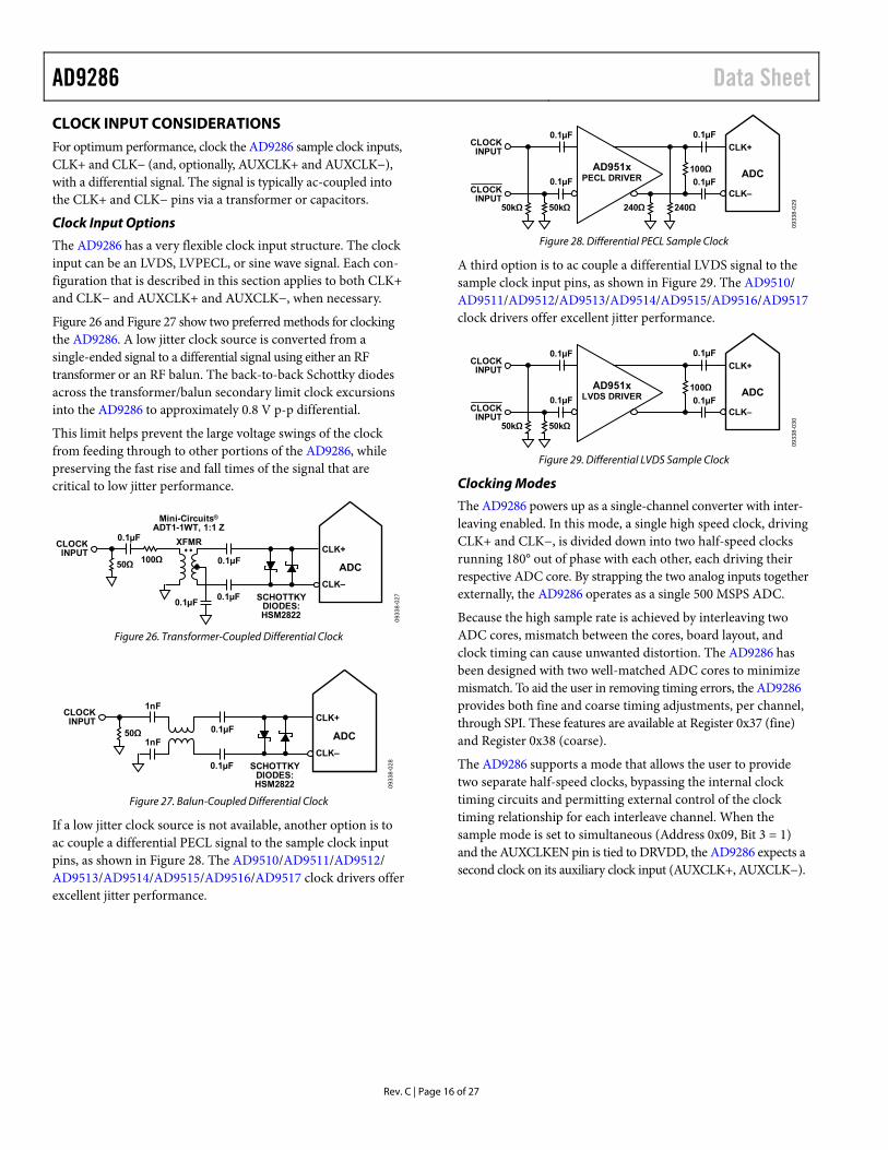
CLOCK INPUT CONSIDERATIONS For optimum performance, clock the AD9286 sample clock inputs, CLK+ and CLK− (and, optionally, AUXCLK+ and AUXCLK−), with a differential signal. The signal is typically ac-coupled into the CLK+ and CLK− pins via a transformer or capacitors.
Clock Input Options
The AD9286 has a very flexible clock input structure. The clock input can be an LVDS, LVPECL, or sine wave signal. Each con-figuration that is described in this section applies to both CLK+ and CLK− and AUXCLK+ and AUXCLK−, when necessary.
Figure 26 and Figure 27 show two preferred methods for clocking the AD9286. A low jitter clock source is converted from a single-ended signal to a differential signal using either an RF transformer or an RF balun. The back-to-back Schottky diodes across the transformer/balun secondary limit clock excursions into the AD9286 to approximately 0.8 V p-p differential.
This limit helps prevent the large voltage swings of the clock from feeding through to other portions of the AD9286, while preserving the fast rise and fall times of the signal that are critical to low jitter performance.
0.1µF0.1µF
0.1µF
0.1µF
SCHOTTKYDIODES:HSM2822
50Ω 100Ω
CLK–
CLK+
ADC
Mini-Circuits®
ADT1-1WT, 1:1 Z
XFMRCLOCKINPUT
0933
8-02
7
Figure 26. Transformer-Coupled Differential Clock
0.1µF
0.1µF
SCHOTTKYDIODES:HSM2822
1nF
1nF50Ω
CLK–
CLK+
ADC
CLOCKINPUT
0933
8-02
8
Figure 27. Balun-Coupled Differential Clock
If a low jitter clock source is not available, another option is to ac couple a differential PECL signal to the sample clock input pins, as shown in Figure 28. The AD9510/AD9511/AD9512/ AD9513/AD9514/AD9515/AD9516/AD9517 clock drivers offer excellent jitter performance.
100Ω
0.1µF
0.1µF0.1µF
0.1µF
240Ω240Ω50kΩ50kΩ
CLK–
CLK+
ADCAD951x
PECL DRIVER
CLOCKINPUT
CLOCKINPUT
0933
8-02
9
Figure 28. Differential PECL Sample Clock
A third option is to ac couple a differential LVDS signal to the sample clock input pins, as shown in Figure 29. The AD9510/ AD9511/AD9512/AD9513/AD9514/AD9515/AD9516/AD9517 clock drivers offer excellent jitter performance.
100Ω
0.1µF
0.1µF0.1µF
0.1µF
50kΩ50kΩ
CLK–
CLK+
ADCAD951x
LVDS DRIVER
CLOCKINPUT
CLOCKINPUT
0933
8-03
0
Figure 29. Differential LVDS Sample Clock
Clocking Modes
The AD9286 powers up as a single-channel converter with inter-leaving enabled. In this mode, a single high speed clock, driving CLK+ and CLK−, is divided down into two half-speed clocks running 180° out of phase with each other, each driving their respective ADC core. By strapping the two analog inputs together externally, the AD9286 operates as a single 500 MSPS ADC.
Because the high sample rate is achieved by interleaving two ADC cores, mismatch between the cores, board layout, and clock timing can cause unwanted distortion. The AD9286 has been designed with two well-matched ADC cores to minimize mismatch. To aid the user in removing timing errors, the AD9286 provides both fine and coarse timing adjustments, per channel, through SPI. These features are available at Register 0x37 (fine) and Register 0x38 (coarse).
The AD9286 supports a mode that allows the user to provide two separate half-speed clocks, bypassing the internal clock timing circuits and permitting external control of the clock timing relationship for each interleave channel. When the sample mode is set to simultaneous (Address 0x09, Bit 3 = 1) and the AUXCLKEN pin is tied to DRVDD, the AD9286 expects a second clock on its auxiliary clock input (AUXCLK+, AUXCLK−).
Data Sheet AD9286 In this mode, the AD9286 can also function as a dual 8-bit, 250 MSPS converter. This may be useful in applications where both a single 8-bit, 500 MSPS and a dual 8-bit, 250 MSPS converter are needed. The clock management block requires that CLK± and AUXCLK± be either 0° or 180°, relative to each other. If this requirement is satisfied, the circuit correctly time aligns the data coming out of each ADC core.
If the user desires to operate the AD9286 as a dual 8-bit, 250 MSPS converter and supply only a single clock, this is achieved by setting sample mode to simultaneous, with the AUXCLKEN pin tied to AGND. In this mode, the two ADC cores sample simultaneously. For a summary of all supported clocking modes, see Table 9.
The AD9286 supports the clocking of each internal ADC with separate clocks. By setting AUXCLKEN to DRVDD, the user can supply a differential auxiliary clock to AUXCLK+ and AUXCLK−. In this mode, each internal ADC core has a maximum sample rate of 250 MSPS. This mode bypasses the internal timing adjustment blocks.
Interleave Performance
The AD9286 achieves 500 MSPS conversion by time interleaving two 250 MSPS ADC channels. Although this technique is sufficient in achieving 8-bit performance, quantifiable errors are introduced. These errors come from three sources: gain mismatch, imperfect out-of-phase sampling, and offset mismatch between the two channels. Distortion appears spectrally in two distinct ways: gain and timing mismatch appear as an alias spur (see Equation 1), and offset mismatch appears as a spur located at the Nyquist rate of the converter (see Equation 2).
fALIAS_SPUR = fS/2 − fIN (1)
where: fS is the interleaved sample rate. fIN is the analog input frequency.
fOFFSET_SPUR = fS/2 (2)
where fS is the interleaved sample rate.
The magnitude of the alias spur (AS) contributed by a gain error is shown in Equation 3.
ASGAIN (dBc) = 20 × log(ASGAIN) = 20 × log(GE/2) (3)
where: GE = Gain_Error_Ratio = 1 − VFS1/VFS2. VFSn is the full-scale voltage of Core n.
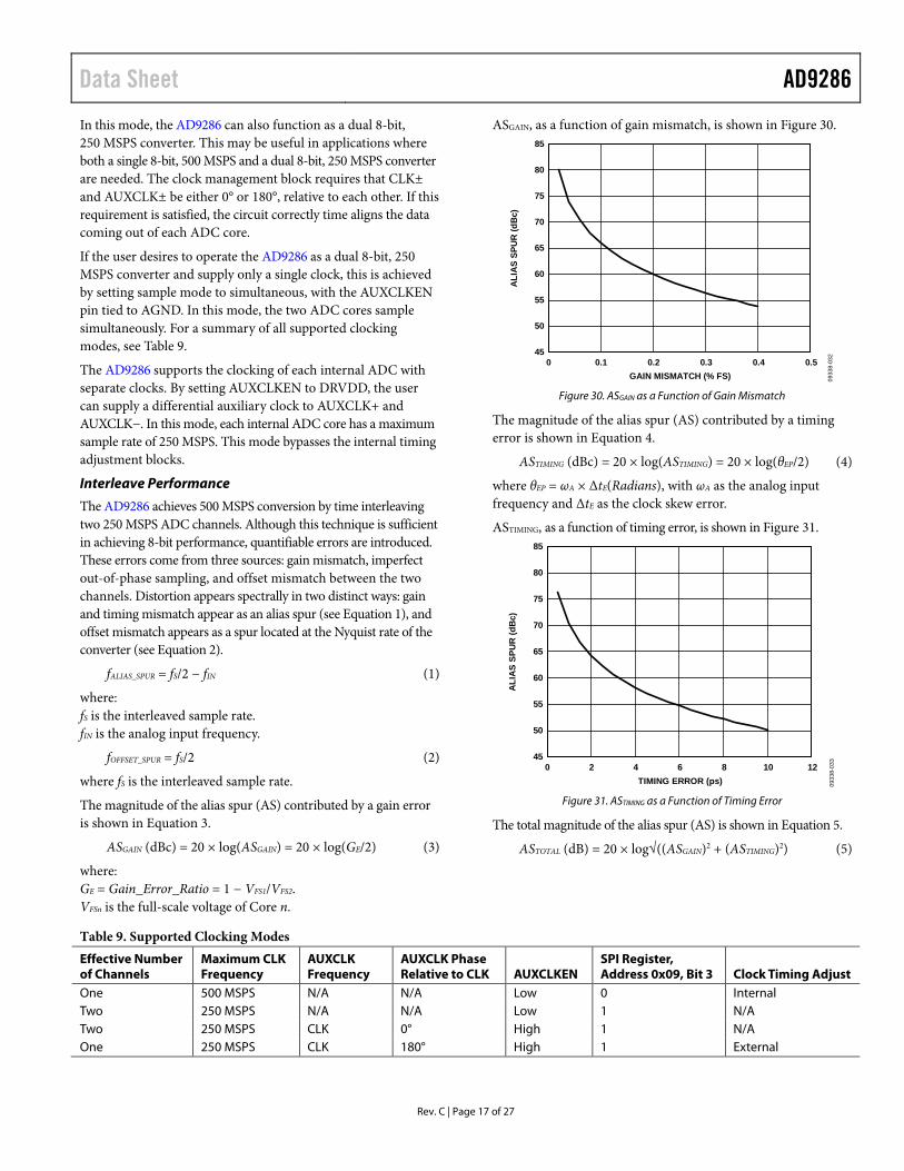
ASGAIN, as a function of gain mismatch, is shown in Figure 30. 85
80
75
70
65
60
55
50
450 0.50.40.30.20.1
ALI
AS
SPU
R (d
Bc)
GAIN MISMATCH (% FS) 0933
8-03
2
Figure 30. ASGAIN as a Function of Gain Mismatch
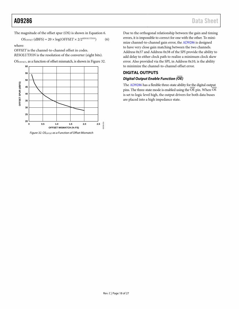
The magnitude of the alias spur (AS) contributed by a timing error is shown in Equation 4.
ASTIMING (dBc) = 20 × log(ASTIMING) = 20 × log(θEP/2) (4)
where θEP = ωA × ∆tE(Radians), with ωA as the analog input frequency and ∆tE as the clock skew error.
ASTIMING, as a function of timing error, is shown in Figure 31. 85
80
75
70
65
60
55
50
450 12108642
ALI
AS
SPU
R (d
Bc)
TIMING ERROR (ps) 0933
8-03
3
Figure 31. ASTIMING as a Function of Timing Error
The total magnitude of the alias spur (AS) is shown in Equation 5.
ASTOTAL (dB) = 20 × log√((ASGAIN)2 + (ASTIMING)2) (5)
Table 9. Supported Clocking Modes Effective Number of Channels
Maximum CLK Frequency
AUXCLK Frequency
AUXCLK Phase Relative to CLK AUXCLKEN
SPI Register, Address 0x09, Bit 3 Clock Timing Adjust
One 500 MSPS N/A N/A Low 0 Internal Two 250 MSPS N/A N/A Low 1 N/A Two 250 MSPS CLK 0° High 1 N/A One 250 MSPS CLK 180° High 1 External
Rev. C | Page 17 of 27
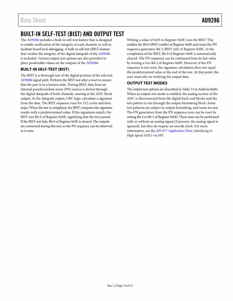
AD9286 Data Sheet The magnitude of the offset spur (OS) is shown in Equation 6.
OSOFFSET (dBFS) = 20 × log(OFFSET × 2/2RESOLUTION) (6)
where: OFFSET is the channel-to-channel offset in codes. RESOLUTION is the resolution of the converter (eight bits).
OSOFFSET, as a function of offset mismatch, is shown in Figure 32. 60
55
50
45
40
35
30
25
200 2.52.01.51.00.5
OFF
SET
SPU
R (d
BFS
)
OFFSET MISMATCH (% FS) 0933
8-03
4
Figure 32. OSOFFSET as a Function of Offset Mismatch
Due to the orthogonal relationship between the gain and timing errors, it is impossible to correct for one with the other. To mini-mize channel-to-channel gain error, the AD9286 is designed to have very close gain matching between the two channels. Address 0x37 and Address 0x38 of the SPI provide the ability to add delay to either clock path to realize a minimum clock skew error. Also provided via the SPI, in Address 0x10, is the ability to minimize the channel-to-channel offset error.
DIGITAL OUTPUTS Digital Output Enable Function (OE)
The AD9286 has a flexible three-state ability for the digital output pins. The three-state mode is enabled using the OE pin. When OE is set to logic level high, the output drivers for both data buses are placed into a high impedance state.
Rev. C | Page 18 of 27
Data Sheet AD9286
BUILT-IN SELF-TEST (BIST) AND OUTPUT TEST The AD9286 includes a built-in self-test feature that is designed to enable verification of the integrity of each channel, as well as facilitate board level debugging. A built-in self-test (BIST) feature that verifies the integrity of the digital datapath of the AD9286 is included. Various output test options are also provided to place predictable values on the outputs of the AD9286.
BUILT-IN SELF-TEST (BIST) The BIST is a thorough test of the digital portion of the selected AD9286 signal path. Perform the BIST test after a reset to ensure that the part is in a known state. During BIST, data from an internal pseudorandom noise (PN) source is driven through the digital datapath of both channels, starting at the ADC block output. At the datapath output, CRC logic calculates a signature from the data. The BIST sequence runs for 512 cycles and then stops. When the test is completed, the BIST compares the signature results with a predetermined value. If the signatures match, the BIST sets Bit 0 of Register 0x0E, signifying that the test passed. If the BIST test fails, Bit 0 of Register 0x0E is cleared. The outputs are connected during this test, so the PN sequence can be observed as it runs.
Writing a value of 0x05 to Register 0x0E runs the BIST. This enables the Bit 0 (BIST enable) of Register 0x0E and resets the PN sequence generator, Bit 2 (BIST init) of Register 0x0E. At the completion of the BIST, Bit 0 of Register 0x0E is automatically cleared. The PN sequence can be continued from its last value by writing a 0 to Bit 2 of Register 0x0E. However, if the PN sequence is not reset, the signature calculation does not equal the predetermined value at the end of the test. At that point, the user must rely on verifying the output data.
OUTPUT TEST MODES The output test options are described in Table 13 at Address 0x0D. When an output test mode is enabled, the analog section of the ADC is disconnected from the digital back-end blocks and the test pattern is run through the output formatting block. Some test patterns are subject to output formatting, and some are not. The PN generators from the PN sequence tests can be reset by setting Bit 4 or Bit 5 of Register 0x0D. These tests can be performed with or without an analog signal (if present, the analog signal is ignored), but they do require an encode clock. For more information, see the AN-877 Application Note, Interfacing to High Speed ADCs via SPI.
Rev. C | Page 19 of 27
AD9286 Data Sheet
Rev. C | Page 20 of 27
SERIAL PORT INTERFACE (SPI) The AD9286 serial port interface (SPI) allows the user to configure the converter for specific functions or operations through a structured register space provided inside the ADC. The SPI gives the user added flexibility and customization, depending on the application. Addresses are accessed via the serial port and can be written to or read from via the port. Memory is organized into bytes that can be further divided into fields, which are documented in the Memory Map section. For detailed operational information, see the AN-877 Application Note, Interfacing to High Speed ADCs via SPI.
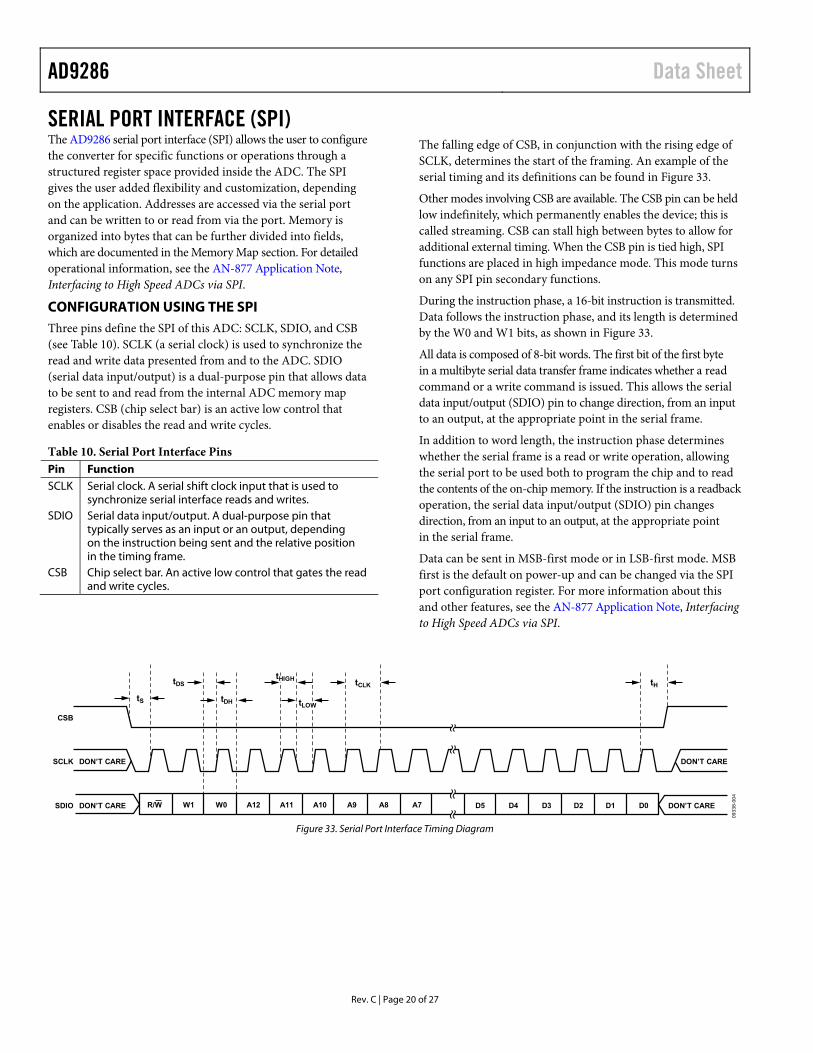
CONFIGURATION USING THE SPI Three pins define the SPI of this ADC: SCLK, SDIO, and CSB (see Table 10). SCLK (a serial clock) is used to synchronize the read and write data presented from and to the ADC. SDIO (serial data input/output) is a dual-purpose pin that allows data to be sent to and read from the internal ADC memory map registers. CSB (chip select bar) is an active low control that enables or disables the read and write cycles.
Table 10. Serial Port Interface Pins Pin Function SCLK Serial clock. A serial shift clock input that is used to
synchronize serial interface reads and writes. SDIO Serial data input/output. A dual-purpose pin that
typically serves as an input or an output, depending on the instruction being sent and the relative position in the timing frame.
CSB Chip select bar. An active low control that gates the read and write cycles.
The falling edge of CSB, in conjunction with the rising edge of SCLK, determines the start of the framing. An example of the serial timing and its definitions can be found in Figure 33.
Other modes involving CSB are available. The CSB pin can be held low indefinitely, which permanently enables the device; this is called streaming. CSB can stall high between bytes to allow for additional external timing. When the CSB pin is tied high, SPI functions are placed in high impedance mode. This mode turns on any SPI pin secondary functions.
During the instruction phase, a 16-bit instruction is transmitted. Data follows the instruction phase, and its length is determined by the W0 and W1 bits, as shown in Figure 33.
All data is composed of 8-bit words. The first bit of the first byte in a multibyte serial data transfer frame indicates whether a read command or a write command is issued. This allows the serial data input/output (SDIO) pin to change direction, from an input to an output, at the appropriate point in the serial frame.
In addition to word length, the instruction phase determines whether the serial frame is a read or write operation, allowing the serial port to be used both to program the chip and to read the contents of the on-chip memory. If the instruction is a readback operation, the serial data input/output (SDIO) pin changes direction, from an input to an output, at the appropriate point in the serial frame.
Data can be sent in MSB-first mode or in LSB-first mode. MSB first is the default on power-up and can be changed via the SPI port configuration register. For more information about this and other features, see the AN-877 Application Note, Interfacing to High Speed ADCs via SPI.
DON’T CARE
DON’T CAREDON’T CARE
DON’T CARE
SDIO
SCLK
CSB
tS tDH
tCLKtDS tH
R/W W1 W0 A12 A11 A10 A9 A8 A7 D5 D4 D3 D2 D1 D0
tLOW
tHIGH
0933
8-00
4
Figure 33. Serial Port Interface Timing Diagram
Data Sheet AD9286
HARDWARE INTERFACE The pins described in Table 10 constitute the physical interface between the programming device of the user and the serial port of the AD9286. The SCLK and CSB pins function as inputs when using the SPI interface. The SDIO pin is bidirectional, functioning as an input during write phases and as an output during readback.
The SPI interface is flexible enough to be controlled by either FPGAs or microcontrollers. One method for SPI configuration is described in detail in the AN-812 Application Note, Micro-controller-Based Serial Port Interface (SPI) Boot Circuit.
The SPI port should not be active during periods when the full dynamic performance of the converter is required. Because the SCLK, CSB, and SDIO signals are typically asynchronous to the ADC clock, noise from these signals can degrade converter performance. If the on-board SPI bus is used for other devices, it may be necessary to provide buffers between this bus and the AD9286 to prevent these signals from transitioning at the converter inputs during critical sampling periods.
SDIO/PWDN serves a dual function when the SPI interface is not being used. When the pin is strapped to AVDD or ground during device power-on, it is associated with a specific function. The mode selection table (see Table 11) describes the strappable functions that are supported on the AD9286.
Table 11. Mode Selection
Pin External Voltage Configuration
SDIO/PWDN AVDD (default) Chip in full power-down AGND Normal operation
OE AVDD Outputs in high impedance AGND (default) Outputs enabled
CONFIGURATION WITHOUT THE SPI In applications that do not interface to the SPI control registers, the SDIO/PWDN pin serves as a standalone, CMOS-compatible control pin. When the device is powered up, it is assumed that the user intends to use the SDIO, SCLK, and CSB pins as static control lines for the output enable and power-down feature control. In this mode, connecting the CSB chip select to AVDD disables the serial port interface.
SPI ACCESSIBLE FEATURES Table 12 provides a brief description of the general features that are accessible via the SPI. These features are described in detail in the AN-877 Application Note, Interfacing to High Speed ADCs via SPI. The AD9286 part-specific features are described in detail in Table 13.
Table 12. Features Accessible Using the SPI Feature Description Mode Allows the user to set either power-down mode
or standby mode Clock Allows the user to access the DCS via the SPI Offset Allows the user to digitally adjust the converter
offset Test I/O Allows the user to set test modes to have known
data on output bits Output Mode Allows the user to set up outputs Output Phase Allows the user to set the output clock polarity Output Delay Allows the user to vary the DCO delay Voltage Reference
Allows the user to set the voltage reference
Rev. C | Page 21 of 27
AD9286 Data Sheet
MEMORY MAP READING THE MEMORY MAP REGISTER TABLE Each row in the memory map register table (see Table 13) has eight bit locations. The memory map is roughly divided into three sections: the chip configuration registers (Address 0x00 to Address 0x02), the device index and transfer registers (Address 0x05 and Address 0xFF), and the program registers (Address 0x08 to Address 0x38).
Table 13 documents the default hexadecimal value for each hexadecimal address shown. The column with the heading Bit 7 (MSB) is the start of the default hexadecimal value given. For more information on this function and others, see the AN-877 Application Note, Interfacing to High Speed ADCs via SPI. This document details the functions controlled by Register 0x00 to Register 0xFF.
Open Locations
All address and bit locations that are not included in the SPI map are not currently supported for this device. Unused bits of a valid address location should be written with 0s. Writing to these locations is required only when part of an address location is open. If the entire address location is open, it is omitted from the SPI map (for example, Address 0x13) and should not be written.
Default Values
After the AD9286 is reset, critical registers are loaded with default values. The default values for the registers are given in the memory map register table (see Table 13).
Logic Levels
An explanation of logic level terminology follows:
• “Bit is set” is synonymous with “bit is set to Logic 1” or“writing Logic 1 for the bit.”
• “Bit is cleared” is synonymous with “bit is set to Logic 0” or“writing Logic 0 for the bit.”
Transfer Register Map
Address 0x08 to Address 0x38 are shadowed. Writes to these addresses do not affect part operation until a transfer command is issued by writing 0x01 to Address 0xFF, setting the transfer bit. Setting the transfer bit allows these registers to be updated internally and simultaneously. The internal update takes place when the transfer bit is set, and then the bit autoclears.
Channel-Specific Registers
Some channel setup functions can be programmed differently for each channel. In these cases, channel address locations are internally duplicated for each channel. These registers and bits are designated in the memory map register table as local. These local registers and bits can be accessed by setting the appropriate Channel 1 (Bit 0) or Channel 2 (Bit 1) bits in Register 0x05.
If both bits are set, the subsequent write affects the registers of both channels. In a read cycle, set only Channel 1 or Channel 2 to read one of the two registers. If both bits are set during an SPI read cycle, the part returns the value for Channel 1. Registers and bits designated as global in the memory map register table affect the entire part or the channel features for which independent settings are not allowed between channels. The settings in Register 0x05 do not affect the global registers and bits.
Rev. C | Page 22 of 27
Data Sheet AD9286
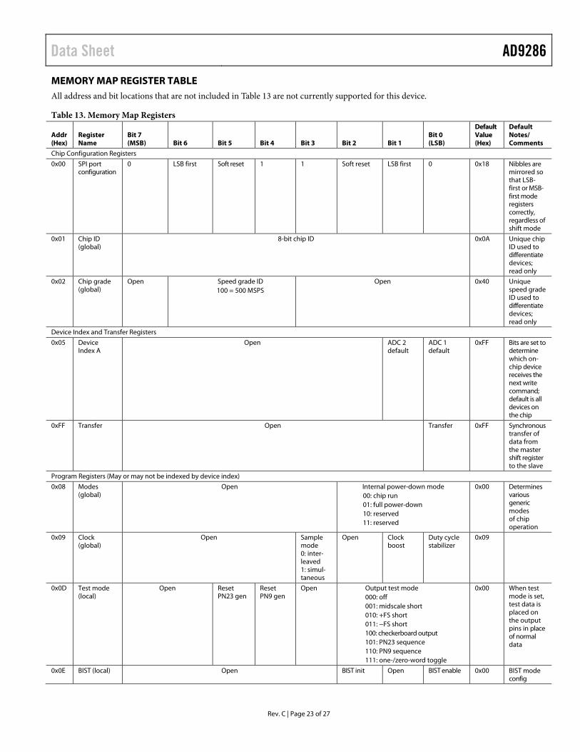
MEMORY MAP REGISTER TABLE All address and bit locations that are not included in Table 13 are not currently supported for this device.
Table 13. Memory Map Registers
Addr (Hex)
Register Name
Bit 7 (MSB) Bit 6 Bit 5 Bit 4 Bit 3 Bit 2 Bit 1
Bit 0 (LSB)
Default Value (Hex)
Default Notes/ Comments
Chip Configuration Registers
0x00 SPI port configuration
0 LSB first Soft reset 1 1 Soft reset LSB first 0 0x18 Nibbles are mirrored so that LSB-first or MSB-first mode registers correctly, regardless of shift mode
0x01 Chip ID (global)
8-bit chip ID 0x0A Unique chip ID used to differentiate devices; read only
0x02 Chip grade (global)
Open Speed grade ID 100 = 500 MSPS
Open 0x40 Unique speed grade ID used to differentiate devices; read only
Device Index and Transfer Registers
0x05 Device Index A
Open ADC 2 default
ADC 1 default
0xFF Bits are set to determine which on-chip device receives the next write command; default is all devices on the chip
0xFF Transfer Open Transfer 0xFF Synchronous transfer of data from the master shift register to the slave
Program Registers (May or may not be indexed by device index)
0x08 Modes (global)
Open Internal power-down mode 00: chip run 01: full power-down 10: reserved 11: reserved
0x00 Determines various generic modes of chip operation
0x09 Clock (global)
Open Sample mode 0: inter-leaved 1: simul-taneous
Open Clock boost
Duty cycle stabilizer
0x09
0x0D Test mode (local)
Open Reset PN23 gen
Reset PN9 gen
Open Output test mode 000: off 001: midscale short 010: +FS short 011: −FS short 100: checkerboard output 101: PN23 sequence 110: PN9 sequence 111: one-/zero-word toggle
0x00 When test mode is set, test data is placed on the output pins in place of normal data
0x0E BIST (local) Open BIST init Open BIST enable 0x00 BIST mode config
Rev. C | Page 23 of 27
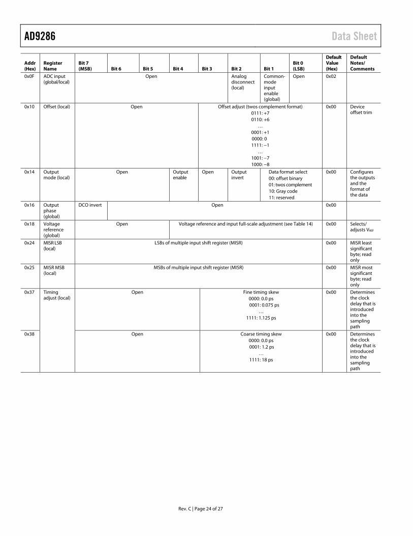
AD9286 Data Sheet
Addr (Hex)
Register Name
Bit 7 (MSB) Bit 6 Bit 5 Bit 4 Bit 3 Bit 2 Bit 1
Bit 0 (LSB)
Default Value (Hex)
Default Notes/ Comments
0x0F ADC input (global/local)
Open Analog disconnect (local)
Common-mode input enable (global)
Open 0x02
0x10 Offset (local) Open Offset adjust (twos complement format) 0111: +7 0110: +6
… 0001: +1 0000: 0 1111: −1
… 1001: −7 1000: −8
0x00 Device offset trim
0x14 Output mode (local)
Open Output enable
Open Output invert
Data format select 00: offset binary 01: twos complement 10: Gray code 11: reserved
0x00 Configures the outputs and the format of the data
0x16 Output phase (global)
DCO invert Open 0x00
0x18 Voltage reference (global)
Open Voltage reference and input full-scale adjustment (see Table 14) 0x00 Selects/ adjusts VREF
0x24 MISR LSB (local)
LSBs of multiple input shift register (MISR) 0x00 MISR least significant byte; read only
0x25 MISR MSB (local)
MSBs of multiple input shift register (MISR) 0x00 MISR most significant byte; read only
0x37 Timing adjust (local)
Open Fine timing skew 0000: 0.0 ps 0001: 0.075 ps
… 1111: 1.125 ps
0x00 Determines the clock delay that is introduced into the sampling path
0x38 Open Coarse timing skew 0000: 0.0 ps 0001: 1.2 ps
… 1111: 18 ps
0x00 Determines the clock delay that is introduced into the sampling path
Rev. C | Page 24 of 27
Data Sheet AD9286
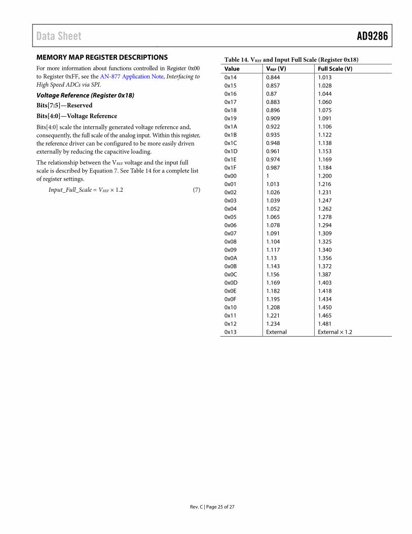
MEMORY MAP REGISTER DESCRIPTIONS For more information about functions controlled in Register 0x00 to Register 0xFF, see the AN-877 Application Note, Interfacing to High Speed ADCs via SPI.
Voltage Reference (Register 0x18)
Bits[7:5]—Reserved Bits[4:0]—Voltage Reference
Bits[4:0] scale the internally generated voltage reference and, consequently, the full scale of the analog input. Within this register, the reference driver can be configured to be more easily driven externally by reducing the capacitive loading.
The relationship between the VREF voltage and the input full scale is described by Equation 7. See Table 14 for a complete list of register settings.
Input_Full_Scale = VREF × 1.2 (7)
Table 14. VREF and Input Full Scale (Register 0x18) Value VREF (V) Full Scale (V) 0x14 0.844 1.013 0x15 0.857 1.028 0x16 0.87 1.044 0x17 0.883 1.060 0x18 0.896 1.075 0x19 0.909 1.091 0x1A 0.922 1.106 0x1B 0.935 1.122 0x1C 0.948 1.138 0x1D 0.961 1.153 0x1E 0.974 1.169 0x1F 0.987 1.184 0x00 1 1.200 0x01 1.013 1.216 0x02 1.026 1.231 0x03 1.039 1.247 0x04 1.052 1.262 0x05 1.065 1.278 0x06 1.078 1.294 0x07 1.091 1.309 0x08 1.104 1.325 0x09 1.117 1.340 0x0A 1.13 1.356 0x0B 1.143 1.372 0x0C 1.156 1.387 0x0D 1.169 1.403 0x0E 1.182 1.418 0x0F 1.195 1.434 0x10 1.208 1.450 0x11 1.221 1.465 0x12 1.234 1.481 0x13 External External × 1.2
Rev. C | Page 25 of 27
AD9286 Data Sheet
APPLICATIONS INFORMATION DESIGN GUIDELINES Before starting design and layout of the AD9286 as a system, it is recommended that the designer become familiar with these guidelines, which discuss the special circuit connections and layout requirements that are needed for certain pins.
Power and Ground Recommendations
When connecting power to the AD9286, it is strongly recom-mended that two separate supplies be used. Use one 1.8 V supply for analog (AVDD); use a separate 1.8 V supply for the digital output supply (DRVDD). If a common 1.8 V AVDD and DRVDD supply must be used, the AVDD and DRVDD domains must be isolated with a ferrite bead or filter choke and separate decoupling capacitors. Several different decoupling capacitors can be used to cover both high and low frequencies. Locate these capacitors close to the point of entry at the printed circuit board (PCB) level and close to the pins of the part, with minimal trace length.
A single PCB ground plane should be sufficient when using the AD9286. With proper decoupling and smart partitioning of the PCB analog, digital, and clock sections, optimum performance is easily achieved.
Exposed Paddle Thermal Heat Sink Recommendations
The exposed paddle (Pin 0) is the only ground connection for the AD9286; therefore, it must be connected to analog ground (AGND) on the customer PCB. To achieve the best electrical and thermal performance, mate an exposed (no solder mask), continuous copper plane on the PCB to the AD9286 exposed paddle, Pin 0.
The copper plane should have several vias to achieve the lowest possible resistive thermal path for heat dissipation to flow through the bottom of the PCB. Fill or plug these vias with nonconductive epoxy.
To maximize the coverage and adhesion between the ADC and the PCB, a silkscreen should be overlaid to partition the continuous plane on the PCB into several uniform sections. This provides several tie points between the ADC and the PCB during the reflow process. Using one continuous plane with no partitions guarantees only one tie point between the ADC and the PCB. For detailed information about packaging and PCB layout of chip scale packages, see the AN-772 Application Note, A Design and Manufacturing Guide for the Lead Frame Chip Scale Package (LFCSP), at www.analog.com.
VCM
The VCM pin should be decoupled to ground with a 0.1 µF capacitor.
RBIAS
The AD9286 requires that a 10 kΩ resistor be placed between the RBIAS pin and ground. This resistor, which sets the master current reference of the ADC core, should have at least a 1% tolerance.
Reference Decoupling
Decouple the VREF pin externally to ground with a low ESR, 1.0 µF capacitor in parallel with a low ESR, 0.1 µF ceramic capacitor.
SPI Port
The SPI port should not be active during periods when the full dynamic performance of the converter is required. Because the SCLK, CSB, and SDIO signals are typically asynchronous to the ADC clock, noise from these signals can degrade converter performance. If the on-board SPI bus is used for other devices, it may be necessary to provide buffers between this bus and the AD9286 to prevent these signals from transitioning at the converter inputs during critical sampling periods.
Rev. C | Page 26 of 27
Data Sheet AD9286
OUTLINE DIMENSIONS
*COMPLIANT TO JEDEC STANDARDS MO-220-VKKD-2WITH EXCEPTION TO EXPOSED PAD DIMENSION
1
48
12
13
37
36
24
25
*4.704.60 SQ4.50
0.500.400.30
0.300.230.18
0.80 MAX0.65 TYP
5.50 REF
COPLANARITY0.08
0.20 REF
1.000.850.80 0.05 MAX
0.02 NOM
SEATINGPLANE
12° MAX
TOP VIEW BOTTOM VIEW
0.60 MAX
0.60 MAX
PIN 1INDICATOR 0.50
REF
PIN 1INDICATOR
0.25 MIN
7.107.00 SQ6.90
6.856.75 SQ6.65
06-0
7-20
12-A
FOR PROPER CONNECTION OFTHE EXPOSED PAD, REFER TOTHE PIN CONFIGURATION ANDFUNCTION DESCRIPTIONSSECTION OF THIS DATA SHEET.
EXPOSEDPAD
Figure 34. 48-Lead Lead Frame Chip Scale Package [LFCSP_VQ]
7 mm × 7 mm Body, Very Thin Quad (CP-48-12)
Dimensions shown in millimeters
ORDERING GUIDE
Model1 Temperature Range Package Description Package Option
AD9286BCPZ-500 −40°C to +85°C 48-Lead Lead Frame Chip Scale Package [LFCSP_VQ] CP-48-12 AD9286BCPZRL7-500 −40°C to +85°C 48-Lead Lead Frame Chip Scale Package [LFCSP_VQ] CP-48-12 AD9286-500EBZ Evaluation Board
1 Z = RoHS Compliant Part.
©2011–2015 Analog Devices, Inc. All rights reserved. Trademarks and registered trademarks are the property of their respective owners. D09338-0-1/15(C)
Rev. C | Page 27 of 27
Related Documents