© 2008 Microchip Technology Inc. DS22060B-page 1 MCP413X/415X/423X/425X Features • Single or Dual Resistor Network options • Potentiometer or Rheostat configuration options • Resistor Network Resolution - 7-bit: 128 Resistors (129 Steps) - 8-bit: 256 Resistors (257 Steps) •R AB Resistances options of: - 5kΩ - 10kΩ - 50kΩ - 100 kΩ • Zero Scale to Full-Scale Wiper operation • Low Wiper Resistance: 75Ω (typical) • Low Tempco: - Absolute (Rheostat): 50 ppm typical (0°C to 70°C) - Ratiometric (Potentiometer): 15 ppm typical • SPI Serial Interface (10 MHz, modes 0,0 & 1,1) - High-Speed Read/Writes to wiper registers - SDI/SDO multiplexing (MCP41X1 only) • Resistor Network Terminal Disconnect Feature via: - Shutdown pin (SHDN ) - Terminal Control (TCON) Register • Brown-out reset protection (1.5V typical) • Serial Interface Inactive current (2.5 uA typical) • High-Voltage Tolerant Digital Inputs: Up to 12.5V • Supports Split Rail Applications • Internal weak pull-up on all digital inputs • Wide Operating Voltage: - 2.7V to 5.5V - Device Characteristics Specified - 1.8V to 5.5V - Device Operation • Wide Bandwidth (-3 dB) Operation: - 2 MHz (typical) for 5.0 kΩ device • Extended temperature range (-40°C to +125°C) Description The MCP41XX and MCP42XX devices offer a wide range of product offerings using an SPI interface. This family of devices support 7-bit and 8-bit resistor networks, and Potentiometer and Rheostat pinouts. Package Types (top view) 1 2 3 4 5 6 7 8 P0W P0B P0A V SS V DD MCP41X1 Single Potentiometer PDIP, SOIC, MSOP CS SDI/SDO SCK 1 2 3 4 5 6 7 8 P0B SDO P0W V DD MCP41X2 Single Rheostat PDIP, SOIC, MSOP 1 2 3 4 11 12 13 14 SHDN SDO WP V DD MCP42X1 Dual Potentiometers PDIP, SOIC, TSSOP 5 6 7 8 9 10 P0W P0B P0A P1A P1W P1B V SS CS SDI SCK V SS CS SDI SCK 4x4 QFN* 1 2 3 4 7 8 9 10 SDO V DD MCP42X2 Dual Rheostat MSOP, DFN 5 6 P0B P0W P1W P1B V SS CS SDI SCK 3x3 DFN* SDI/SDO SCK V SS P0B P0W 1 2 3 4 8 7 6 5 P0A CS EP 9 3x3 DFN* SDI SCK V SS SDO P0B 1 2 3 4 8 7 6 5 P0W V DD CS EP 9 V DD 3x3 DFN* SDI SCK V SS SDO P0B 1 2 3 4 10 9 8 7 P0W CS EP 11 V DD 5 6 P1B P1W * Includes Exposed Thermal Pad (EP); see Table 3-1. 2 V SS V SS SCK WP NC P1B P0B P1W P1A P0A P0W CS V DD SDO SHDN SDI EP 16 1 15 14 13 3 4 12 11 10 9 5 6 7 8 17 7/8-Bit Single/Dual SPI Digital POT with Volatile Memory

Welcome message from author
This document is posted to help you gain knowledge. Please leave a comment to let me know what you think about it! Share it to your friends and learn new things together.
Transcript
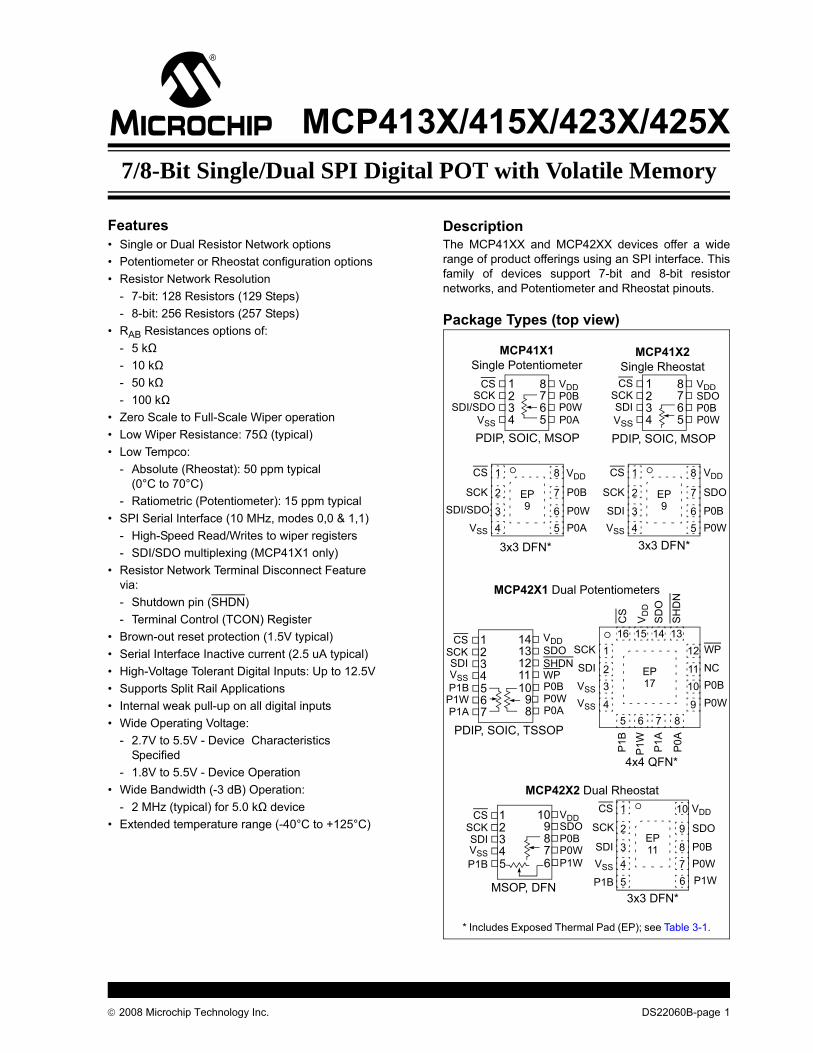
MCP413X/415X/423X/425X7/8-Bit Single/Dual SPI Digital POT with Volatile Memory
Features• Single or Dual Resistor Network options• Potentiometer or Rheostat configuration options• Resistor Network Resolution
- 7-bit: 128 Resistors (129 Steps)- 8-bit: 256 Resistors (257 Steps)
• RAB Resistances options of:- 5 kΩ - 10 kΩ - 50 kΩ - 100 kΩ
• Zero Scale to Full-Scale Wiper operation• Low Wiper Resistance: 75Ω (typical)• Low Tempco:
- Absolute (Rheostat): 50 ppm typical(0°C to 70°C)
- Ratiometric (Potentiometer): 15 ppm typical• SPI Serial Interface (10 MHz, modes 0,0 & 1,1)
- High-Speed Read/Writes to wiper registers- SDI/SDO multiplexing (MCP41X1 only)
• Resistor Network Terminal Disconnect Feature via:- Shutdown pin (SHDN) - Terminal Control (TCON) Register
• Brown-out reset protection (1.5V typical)• Serial Interface Inactive current (2.5 uA typical)• High-Voltage Tolerant Digital Inputs: Up to 12.5V• Supports Split Rail Applications • Internal weak pull-up on all digital inputs • Wide Operating Voltage:
- 2.7V to 5.5V - Device Characteristics Specified
- 1.8V to 5.5V - Device Operation• Wide Bandwidth (-3 dB) Operation:
- 2 MHz (typical) for 5.0 kΩ device • Extended temperature range (-40°C to +125°C)
DescriptionThe MCP41XX and MCP42XX devices offer a widerange of product offerings using an SPI interface. Thisfamily of devices support 7-bit and 8-bit resistornetworks, and Potentiometer and Rheostat pinouts.
Package Types (top view)
1234 5
678
P0WP0B
P0AVSS
VDD
MCP41X1 Single Potentiometer
PDIP, SOIC, MSOP
CS
SDI/SDOSCK
1234 5
678
P0BSDO
P0W
VDD
MCP41X2 Single Rheostat
PDIP, SOIC, MSOP
1234 11
121314
SHDNSDO
WP
VDD
MCP42X1 Dual Potentiometers
PDIP, SOIC, TSSOP
567 8
910
P0WP0B
P0AP1AP1WP1B
VSS
CS
SDISCK
VSS
CS
SDISCK
4x4 QFN*
1234 7
89
10SDOVDD
MCP42X2 Dual Rheostat
MSOP, DFN
5 6
P0BP0WP1WP1B
VSS
CS
SDISCK
3x3 DFN*
SDI/SDOSCK
VSS
P0B
P0W
1
2
34
8
7
65 P0A
CS
EP9
3x3 DFN*
SDI
SCK
VSS
SDO
P0B
1
2
34
8
7
65 P0W
VDDCS
EP9
VDD
3x3 DFN*
SDI
SCK
VSS
SDO
P0B
1
2
34
10
9
87 P0W
CS
EP11
VDD
5 6P1B P1W
* Includes Exposed Thermal Pad (EP); see Table 3-1.
2VSS
VSS
SCK WP
NC
P1B
P0B
P1W P1
A
P0A
P0W
CS
VD
D
SD
O
SH
DN
SDI EP
161
15 14 13
3
4
12
1110
95 6 7 8
17
© 2008 Microchip Technology Inc. DS22060B-page 1

MCP413X/415X/423X/425X
Device Block DiagramDevice Features
Device
# of
PO
Ts
Wiper Configuration
Con
trol
In
terf
ace
Mem
ory
Type
Wip
erLo
ck
Tech
nolo
gy
POR
Wip
er
Setti
ng Resistance (typical)
# of
Ste
ps VDD Operating Range (2) RAB Options (kΩ)
Wiper - RW (Ω)
MCP4131 (3) 1 Potentiometer (1) SPI RAM No Mid-Scale 5.0, 10.0, 50.0, 100.0 75 129 1.8V to 5.5VMCP4132 (3) 1 Rheostat SPI RAM No Mid-Scale 5.0, 10.0, 50.0, 100.0 75 129 1.8V to 5.5VMCP4141 1 Potentiometer (1) SPI EE Yes NV Wiper 5.0, 10.0, 50.0, 100.0 75 129 2.7V to 5.5VMCP4142 1 Rheostat SPI EE Yes NV Wiper 5.0, 10.0, 50.0, 100.0 75 129 2.7V to 5.5VMCP4151 (3) 1 Potentiometer (1) SPI RAM No Mid-Scale 5.0, 10.0, 50.0, 100.0 75 257 1.8V to 5.5VMCP4152 (3) 1 Rheostat SPI RAM No Mid-Scale 5.0, 10.0, 50.0, 100.0 75 257 1.8V to 5.5VMCP4161 1 Potentiometer (1) SPI EE Yes NV Wiper 5.0, 10.0, 50.0, 100.0 75 257 2.7V to 5.5VMCP4162 1 Rheostat SPI EE Yes NV Wiper 5.0, 10.0, 50.0, 100.0 75 257 2.7V to 5.5VMCP4231 (3) 2 Potentiometer (1) SPI RAM No Mid-Scale 5.0, 10.0, 50.0, 100.0 75 129 1.8V to 5.5VMCP4232 (3) 2 Rheostat SPI RAM No Mid-Scale 5.0, 10.0, 50.0, 100.0 75 129 1.8V to 5.5VMCP4241 2 Potentiometer (1) SPI EE Yes NV Wiper 5.0, 10.0, 50.0, 100.0 75 129 2.7V to 5.5VMCP4242 2 Rheostat SPI EE Yes NV Wiper 5.0, 10.0, 50.0, 100.0 75 129 2.7V to 5.5VMCP4251 (3) 2 Potentiometer (1) SPI RAM No Mid-Scale 5.0, 10.0, 50.0, 100.0 75 257 1.8V to 5.5VMCP4252 (3) 2 Rheostat SPI RAM No Mid-Scale 5.0, 10.0, 50.0, 100.0 75 257 1.8V to 5.5VMCP4261 2 Potentiometer (1) SPI EE Yes NV Wiper 5.0, 10.0, 50.0, 100.0 75 257 2.7V to 5.5VMCP4262 2 Rheostat SPI EE Yes NV Wiper 5.0, 10.0, 50.0, 100.0 75 257 2.7V to 5.5VNote 1: Floating either terminal (A or B) allows the device to be used as a Rheostat (variable resistor).
2: Analog characteristics only tested from 2.7V to 5.5V unless otherwise noted.3: Please check Microchip web site for device release and availability.
Power-up/Brown-outControl
VDD
VSS
SPI SerialInterfaceModule &ControlLogic(WiperLock™ Technology)
ResistorNetwork 0(Pot 0)
Wiper 0 & TCONRegister
ResistorNetwork 1(Pot 1)
Wiper 1 & TCONRegister
CS SCK SDI
SDO
NC SHDN
Memory (4x9)Wiper0Wiper1TCONSTATUS
P0A
P0W
P0B
P1A
P1W
P1B
For Dual Resistor Network Devices Only
For Dual PotentiometerDevices Only
DS22060B-page 2 © 2008 Microchip Technology Inc.

MCP413X/415X/423X/425X
1.0 ELECTRICAL CHARACTERISTICS
Absolute Maximum Ratings †Voltage on VDD with respect to VSS ............... -0.6V to +7.0VVoltage on CS, SCK, SDI, SDI/SDO, and SHDN with respect to VSS ...................................... -0.6V to 12.5VVoltage on all other pins (PxA, PxW, PxB, and SDO) with respect to VSS ............................ -0.3V to VDD + 0.3VInput clamp current, IIK (VI < 0, VI > VDD, VI > VPP ON HV pins) ......................±20 mAOutput clamp current, IOK (VO < 0 or VO > VDD) ..................................................±20 mAMaximum output current sunk by any Output pin ......................................................................................25 mAMaximum output current sourced by any Output pin ......................................................................................25 mAMaximum current out of VSS pin .................................100 mAMaximum current into VDD pin ....................................100 mAMaximum current into PXA, PXW & PXB pins ............±2.5 mAStorage temperature ....................................-65°C to +150°CAmbient temperature with power applied .....................................................................-40°C to +125°CTotal power dissipation (Note 1) ................................400 mWSoldering temperature of leads (10 seconds) ............. +300°CESD protection on all pins .................................. ≥ 4 kV (HBM),.......................................................................... ≥ 300V (MM)Maximum Junction Temperature (TJ) ......................... +150°C
† Notice: Stresses above those listed under “MaximumRatings” may cause permanent damage to the device. This isa stress rating only and functional operation of the device atthose or any other conditions above those indicated in theoperational listings of this specification is not implied.Exposure to maximum rating conditions for extended periodsmay affect device reliability.
Note 1: Power dissipation is calculated as follows: Pdis = VDD x IDD - ∑ IOH + ∑ (VDD-VOH) x IOH + ∑(VOl x IOL)
© 2008 Microchip Technology Inc. DS22060B-page 3
MCP413X/415X/423X/425X
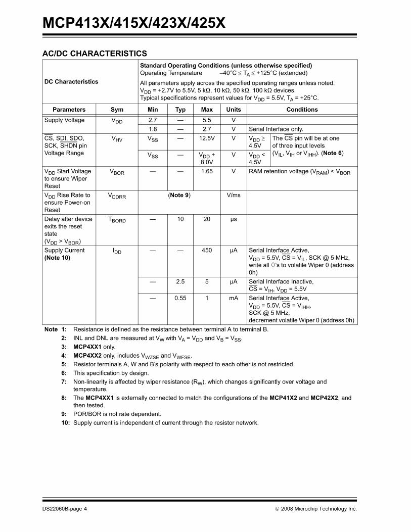
AC/DC CHARACTERISTICS
DC Characteristics
Standard Operating Conditions (unless otherwise specified)Operating Temperature –40°C ≤ TA ≤ +125°C (extended)
All parameters apply across the specified operating ranges unless noted. VDD = +2.7V to 5.5V, 5 kΩ, 10 kΩ, 50 kΩ, 100 kΩ devices. Typical specifications represent values for VDD = 5.5V, TA = +25°C.
Parameters Sym Min Typ Max Units Conditions
Supply Voltage VDD 2.7 — 5.5 V1.8 — 2.7 V Serial Interface only.
CS, SDI, SDO, SCK, SHDN pin Voltage Range
VHV VSS — 12.5V V VDD ≥ 4.5V
The CS pin will be at one of three input levels (VIL, VIH or VIHH). (Note 6)VSS — VDD +
8.0VV VDD <
4.5VVDD Start Voltage to ensure Wiper Reset
VBOR — — 1.65 V RAM retention voltage (VRAM) < VBOR
VDD Rise Rate to ensure Power-on Reset
VDDRR (Note 9) V/ms
Delay after device exits the reset state (VDD > VBOR)
TBORD — 10 20 µs
Supply Current (Note 10)
IDD — — 450 µA Serial Interface Active, VDD = 5.5V, CS = VIL, SCK @ 5 MHz, write all 0’s to volatile Wiper 0 (address 0h)
— 2.5 5 µA Serial Interface Inactive, CS = VIH, VDD = 5.5V
— 0.55 1 mA Serial Interface Active, VDD = 5.5V, CS = VIHH, SCK @ 5 MHz, decrement volatile Wiper 0 (address 0h)
Note 1: Resistance is defined as the resistance between terminal A to terminal B.2: INL and DNL are measured at VW with VA = VDD and VB = VSS. 3: MCP4XX1 only.4: MCP4XX2 only, includes VWZSE and VWFSE.5: Resistor terminals A, W and B’s polarity with respect to each other is not restricted.6: This specification by design.7: Non-linearity is affected by wiper resistance (RW), which changes significantly over voltage and
temperature. 8: The MCP4XX1 is externally connected to match the configurations of the MCP41X2 and MCP42X2, and
then tested.9: POR/BOR is not rate dependent.10: Supply current is independent of current through the resistor network.
DS22060B-page 4 © 2008 Microchip Technology Inc.

MCP413X/415X/423X/425X
Resistance(± 20%)
RAB 4.0 5 6.0 kΩ -502 devices (Note 1)8.0 10 12.0 kΩ -103 devices (Note 1)40.0 50 60.0 kΩ -503 devices (Note 1)80.0 100 120.0 kΩ -104 devices (Note 1)
Resolution N 257 Taps 8-bit No Missing Codes129 Taps 7-bit No Missing Codes
Step Resistance RS — RAB / (256)
— Ω 8-bit Note 6
— RAB / (128)
— Ω 7-bit Note 6
Nominal Resistance Match
|RAB0 - RAB1| / RAB
— 0.2 1.25 % MCP42X1 devices only
|RBW0 - RBW1| / RBW
— 0.25 1.5 % MCP42X2 devices only, Code = Full-Scale
Wiper Resistance (Note 3, Note 4)
RW — 75 160 Ω VDD = 5.5 V, IW = 2.0 mA, code = 00h— 75 300 Ω VDD = 2.7 V, IW = 2.0 mA, code = 00h
Nominal Resistance Tempco
ΔRAB/ΔT — 50 — ppm/°C TA = -20°C to +70°C— 100 — ppm/°C TA = -40°C to +85°C— 150 — ppm/°C TA = -40°C to +125°C
Ratiometeric Tempco
ΔVWB/ΔT — 15 — ppm/°C Code = Midscale (80h or 40h)
Resistor Terminal Input Voltage Range (Terminals A, B and W)
VA,VW,VB VSS — VDD V Note 5, Note 6
Maximum current through A, W or B
IW — — 2.5 mA Note 6, Worst case current through wiper when wiper is either Full-Scale or Zero Scale.
Leakage current into A, W or B
IWL — 100 — nA MCP4XX1 PxA = PxW = PxB = VSS— 100 — nA MCP4XX2 PxB = PxW = VSS
AC/DC CHARACTERISTICS (CONTINUED)
DC Characteristics
Standard Operating Conditions (unless otherwise specified)Operating Temperature –40°C ≤ TA ≤ +125°C (extended)
All parameters apply across the specified operating ranges unless noted. VDD = +2.7V to 5.5V, 5 kΩ, 10 kΩ, 50 kΩ, 100 kΩ devices. Typical specifications represent values for VDD = 5.5V, TA = +25°C.
Parameters Sym Min Typ Max Units Conditions
Note 1: Resistance is defined as the resistance between terminal A to terminal B.2: INL and DNL are measured at VW with VA = VDD and VB = VSS. 3: MCP4XX1 only.4: MCP4XX2 only, includes VWZSE and VWFSE.5: Resistor terminals A, W and B’s polarity with respect to each other is not restricted.6: This specification by design.7: Non-linearity is affected by wiper resistance (RW), which changes significantly over voltage and
temperature. 8: The MCP4XX1 is externally connected to match the configurations of the MCP41X2 and MCP42X2, and
then tested.9: POR/BOR is not rate dependent.10: Supply current is independent of current through the resistor network.
© 2008 Microchip Technology Inc. DS22060B-page 5
MCP413X/415X/423X/425X
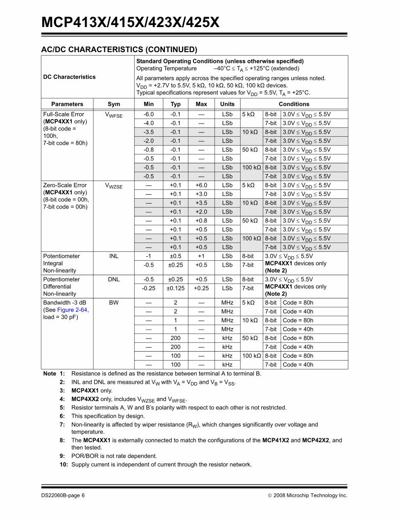
Full-Scale Error (MCP4XX1 only)(8-bit code = 100h, 7-bit code = 80h)
VWFSE -6.0 -0.1 — LSb 5 kΩ 8-bit 3.0V ≤ VDD ≤ 5.5V -4.0 -0.1 — LSb 7-bit 3.0V ≤ VDD ≤ 5.5V-3.5 -0.1 — LSb 10 kΩ 8-bit 3.0V ≤ VDD ≤ 5.5V-2.0 -0.1 — LSb 7-bit 3.0V ≤ VDD ≤ 5.5V-0.8 -0.1 — LSb 50 kΩ 8-bit 3.0V ≤ VDD ≤ 5.5V-0.5 -0.1 — LSb 7-bit 3.0V ≤ VDD ≤ 5.5V-0.5 -0.1 — LSb 100 kΩ 8-bit 3.0V ≤ VDD ≤ 5.5V-0.5 -0.1 — LSb 7-bit 3.0V ≤ VDD ≤ 5.5V
Zero-Scale Error (MCP4XX1 only)(8-bit code = 00h, 7-bit code = 00h)
VWZSE — +0.1 +6.0 LSb 5 kΩ 8-bit 3.0V ≤ VDD ≤ 5.5V— +0.1 +3.0 LSb 7-bit 3.0V ≤ VDD ≤ 5.5V— +0.1 +3.5 LSb 10 kΩ 8-bit 3.0V ≤ VDD ≤ 5.5V— +0.1 +2.0 LSb 7-bit 3.0V ≤ VDD ≤ 5.5V— +0.1 +0.8 LSb 50 kΩ 8-bit 3.0V ≤ VDD ≤ 5.5V— +0.1 +0.5 LSb 7-bit 3.0V ≤ VDD ≤ 5.5V— +0.1 +0.5 LSb 100 kΩ 8-bit 3.0V ≤ VDD ≤ 5.5V— +0.1 +0.5 LSb 7-bit 3.0V ≤ VDD ≤ 5.5V
Potentiometer Integral Non-linearity
INL -1 ±0.5 +1 LSb 8-bit 3.0V ≤ VDD ≤ 5.5V MCP4XX1 devices only (Note 2)
-0.5 ±0.25 +0.5 LSb 7-bit
Potentiometer Differential Non-linearity
DNL -0.5 ±0.25 +0.5 LSb 8-bit 3.0V ≤ VDD ≤ 5.5V MCP4XX1 devices only (Note 2)
-0.25 ±0.125 +0.25 LSb 7-bit
Bandwidth -3 dB (See Figure 2-64, load = 30 pF)
BW — 2 — MHz 5 kΩ 8-bit Code = 80h — 2 — MHz 7-bit Code = 40h — 1 — MHz 10 kΩ 8-bit Code = 80h — 1 — MHz 7-bit Code = 40h — 200 — kHz 50 kΩ 8-bit Code = 80h — 200 — kHz 7-bit Code = 40h — 100 — kHz 100 kΩ 8-bit Code = 80h — 100 — kHz 7-bit Code = 40h
AC/DC CHARACTERISTICS (CONTINUED)
DC Characteristics
Standard Operating Conditions (unless otherwise specified)Operating Temperature –40°C ≤ TA ≤ +125°C (extended)
All parameters apply across the specified operating ranges unless noted. VDD = +2.7V to 5.5V, 5 kΩ, 10 kΩ, 50 kΩ, 100 kΩ devices. Typical specifications represent values for VDD = 5.5V, TA = +25°C.
Parameters Sym Min Typ Max Units Conditions
Note 1: Resistance is defined as the resistance between terminal A to terminal B.2: INL and DNL are measured at VW with VA = VDD and VB = VSS. 3: MCP4XX1 only.4: MCP4XX2 only, includes VWZSE and VWFSE.5: Resistor terminals A, W and B’s polarity with respect to each other is not restricted.6: This specification by design.7: Non-linearity is affected by wiper resistance (RW), which changes significantly over voltage and
temperature. 8: The MCP4XX1 is externally connected to match the configurations of the MCP41X2 and MCP42X2, and
then tested.9: POR/BOR is not rate dependent.10: Supply current is independent of current through the resistor network.
DS22060B-page 6 © 2008 Microchip Technology Inc.
MCP413X/415X/423X/425X
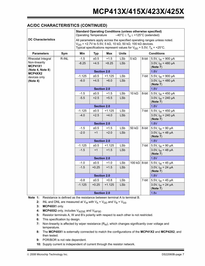
Rheostat Integral Non-linearity MCP41X1 (Note 4, Note 8) MCP4XX2 devices only (Note 4)
R-INL -1.5 ±0.5 +1.5 LSb 5 kΩ 8-bit 5.5V, IW = 900 µA-8.25 +4.5 +8.25 LSb 3.0V, IW = 480 µA
(Note 7)Section 2.0 1.8V
-1.125 ±0.5 +1.125 LSb 7-bit 5.5V, IW = 900 µA -6.0 +4.5 +6.0 LSb 3.0V, IW = 480 µA
(Note 7)Section 2.0 1.8V
-1.5 ±0.5 +1.5 LSb 10 kΩ 8-bit 5.5V, IW = 450 µA-5.5 +2.5 +5.5 LSb 3.0V, IW = 240 µA
(Note 7)Section 2.0 1.8V
-1.125 ±0.5 +1.125 LSb 7-bit 5.5V, IW = 450 µA-4.0 +2.5 +4.0 LSb 3.0V, IW = 240 µA
(Note 7)Section 2.0 1.8V
-1.5 ±0.5 +1.5 LSb 50 kΩ 8-bit 5.5V, IW = 90 µA-2.0 +1 +2.0 LSb 3.0V, IW = 48 µA
(Note 7)Section 2.0 1.8V
-1.125 ±0.5 +1.125 LSb 7-bit 5.5V, IW = 90 µA-1.5 +1 +1.5 LSb 3.0V, IW = 48 µA
(Note 7)Section 2.0 1.8V
-1.0 ±0.5 +1.0 LSb 100 kΩ 8-bit 5.5V, IW = 45 µA-1.5 +0.25 +1.5 LSb 3.0V, IW = 24 µA
(Note 7)Section 2.0 1.8V
-0.8 ±0.5 +0.8 LSb 7-bit 5.5V, IW = 45 µA-1.125 +0.25 +1.125 LSb 3.0V, IW = 24 µA
(Note 7)Section 2.0 1.8v
AC/DC CHARACTERISTICS (CONTINUED)
DC Characteristics
Standard Operating Conditions (unless otherwise specified)Operating Temperature –40°C ≤ TA ≤ +125°C (extended)
All parameters apply across the specified operating ranges unless noted. VDD = +2.7V to 5.5V, 5 kΩ, 10 kΩ, 50 kΩ, 100 kΩ devices. Typical specifications represent values for VDD = 5.5V, TA = +25°C.
Parameters Sym Min Typ Max Units Conditions
Note 1: Resistance is defined as the resistance between terminal A to terminal B.2: INL and DNL are measured at VW with VA = VDD and VB = VSS. 3: MCP4XX1 only.4: MCP4XX2 only, includes VWZSE and VWFSE.5: Resistor terminals A, W and B’s polarity with respect to each other is not restricted.6: This specification by design.7: Non-linearity is affected by wiper resistance (RW), which changes significantly over voltage and
temperature. 8: The MCP4XX1 is externally connected to match the configurations of the MCP41X2 and MCP42X2, and
then tested.9: POR/BOR is not rate dependent.10: Supply current is independent of current through the resistor network.
© 2008 Microchip Technology Inc. DS22060B-page 7

MCP413X/415X/423X/425X
Rheostat Differential Non-linearity MCP41X1 (Note 4, Note 8) MCP4XX2 devices only (Note 4)
R-DNL -0.5 ±0.25 +0.5 LSb 5 kΩ 8-bit 5.5V, IW = 900 µA-1.0 +0.5 +1.0 LSb 3.0V (Note 7)
Section 2.0 1.8V-0.375 ±0.25 +0.375 LSb 7-bit 5.5V, IW = 900 µA-0.75 +0.5 +0.75 LSb 3.0V (Note 7)
Section 2.0 1.8V-0.5 ±0.25 +0.5 LSb 10 kΩ 8-bit 5.5V, IW = 450 µA-1.0 +0.25 +1.0 LSb 3.0V (Note 7)
Section 2.0 1.8V-0.375 ±0.25 +0.375 LSb 7-bit 5.5V, IW = 450 µA-0.75 +0.5 +0.75 LSb 3.0V (Note 7)
Section 2.0 1.8V-0.5 ±0.25 +0.5 LSb 50 kΩ 8-bit 5.5V, IW = 90 µA-0.5 ±0.25 +0.5 LSb 3.0V (Note 7)
Section 2.0 1.8V-0.375 ±0.25 +0.375 LSb 7-bit 5.5V, IW = 90 µA-0.375 ±0.25 +0.375 LSb 3.0V (Note 7)
Section 2.0 1.8V-0.5 ±0.25 +0.5 LSb 100 kΩ 8-bit 5.5V, IW = 45 µA-0.5 ±0.25 +0.5 LSb 3.0V (Note 7)
Section 2.0 1.8V-0.375 ±0.25 +0.375 LSb 7-bit 5.5V, IW = 45 µA-0.375 ±0.25 +0.375 LSb 3.0V (Note 7)
1.8VCapacitance (PA) CAW — 75 — pF f =1 MHz, Code = Full-Scale Capacitance (Pw) CW — 120 — pF f =1 MHz, Code = Full-Scale Capacitance (PB) CBW — 75 — pF f =1 MHz, Code = Full-Scale
AC/DC CHARACTERISTICS (CONTINUED)
DC Characteristics
Standard Operating Conditions (unless otherwise specified)Operating Temperature –40°C ≤ TA ≤ +125°C (extended)
All parameters apply across the specified operating ranges unless noted. VDD = +2.7V to 5.5V, 5 kΩ, 10 kΩ, 50 kΩ, 100 kΩ devices. Typical specifications represent values for VDD = 5.5V, TA = +25°C.
Parameters Sym Min Typ Max Units Conditions
Note 1: Resistance is defined as the resistance between terminal A to terminal B.2: INL and DNL are measured at VW with VA = VDD and VB = VSS. 3: MCP4XX1 only.4: MCP4XX2 only, includes VWZSE and VWFSE.5: Resistor terminals A, W and B’s polarity with respect to each other is not restricted.6: This specification by design.7: Non-linearity is affected by wiper resistance (RW), which changes significantly over voltage and
temperature. 8: The MCP4XX1 is externally connected to match the configurations of the MCP41X2 and MCP42X2, and
then tested.9: POR/BOR is not rate dependent.10: Supply current is independent of current through the resistor network.
DS22060B-page 8 © 2008 Microchip Technology Inc.

MCP413X/415X/423X/425X
Digital Inputs/Outputs (CS, SDI, SDO, SCK, SHDN)Schmitt Trigger High Input Threshold
VIH 0.45 VDD — — V 2.7V ≤ VDD ≤ 5.5V (Allows 2.7V Digital VDD with 5V Analog VDD)
0.5 VDD — — V 1.8V ≤ VDD ≤ 2.7VSchmitt Trigger Low Input Threshold
VIL — — 0.2VDD V
Hysteresis of Schmitt Trigger Inputs
VHYS — 0.1VDD — V
High Voltage Limit VMAX — — 12.5 (6) V Pin can tolerate VMAX or less. Output Low Voltage (SDO)
VOL VSS — 0.3VDD V IOL = 5 mA, VDD = 5.5V VSS — 0.3VDD V IOL = 1 mA, VDD = 1.8V
Output High Voltage (SDO)
VOH 0.7VDD — VDD V IOH = -2.5 mA, VDD = 5.5V 0.7VDD — VDD V IOL = -1 mA, VDD = 1.8V
Weak Pull-up / Pull-down Current
IPU — — 1.75 mA Internal VDD pull-up, VIHH pull-down, VDD = 5.5V, VCS = 12.5V
— 170 — µA CS pin, VDD = 5.5V, VCS = 3V CS Pull-up /Pull-down Resistance
RCS — 16 — kΩ VDD = 5.5V, VCS = 3V
Input Leakage Current
IIL -1 — 1 µA VIN = VDD and VIN = VSS
Pin Capacitance CIN, COUT — 10 — pF fC = 20 MHzRAM (Wiper) ValueValue Range N 0h — 1FFh hex 8-bit device
0h — 1FFh hex 7-bit devicePOR/BOR Value N — 80h — hex 8-bit device
— 40h — hex 7-bit device
AC/DC CHARACTERISTICS (CONTINUED)
DC Characteristics
Standard Operating Conditions (unless otherwise specified)Operating Temperature –40°C ≤ TA ≤ +125°C (extended)
All parameters apply across the specified operating ranges unless noted. VDD = +2.7V to 5.5V, 5 kΩ, 10 kΩ, 50 kΩ, 100 kΩ devices. Typical specifications represent values for VDD = 5.5V, TA = +25°C.
Parameters Sym Min Typ Max Units Conditions
Note 1: Resistance is defined as the resistance between terminal A to terminal B.2: INL and DNL are measured at VW with VA = VDD and VB = VSS. 3: MCP4XX1 only.4: MCP4XX2 only, includes VWZSE and VWFSE.5: Resistor terminals A, W and B’s polarity with respect to each other is not restricted.6: This specification by design.7: Non-linearity is affected by wiper resistance (RW), which changes significantly over voltage and
temperature. 8: The MCP4XX1 is externally connected to match the configurations of the MCP41X2 and MCP42X2, and
then tested.9: POR/BOR is not rate dependent.10: Supply current is independent of current through the resistor network.
© 2008 Microchip Technology Inc. DS22060B-page 9

MCP413X/415X/423X/425X
Power RequirementsPower Supply Sensitivity (MCP41X2 and MCP42X2 only)
PSS — 0.0015 0.0035 %/% 8-bit VDD = 2.7V to 5.5V, VA = 2.7V, Code = 80h
— 0.0015 0.0035 %/% 7-bit VDD = 2.7V to 5.5V, VA = 2.7V, Code = 40h
AC/DC CHARACTERISTICS (CONTINUED)
DC Characteristics
Standard Operating Conditions (unless otherwise specified)Operating Temperature –40°C ≤ TA ≤ +125°C (extended)
All parameters apply across the specified operating ranges unless noted. VDD = +2.7V to 5.5V, 5 kΩ, 10 kΩ, 50 kΩ, 100 kΩ devices. Typical specifications represent values for VDD = 5.5V, TA = +25°C.
Parameters Sym Min Typ Max Units Conditions
Note 1: Resistance is defined as the resistance between terminal A to terminal B.2: INL and DNL are measured at VW with VA = VDD and VB = VSS. 3: MCP4XX1 only.4: MCP4XX2 only, includes VWZSE and VWFSE.5: Resistor terminals A, W and B’s polarity with respect to each other is not restricted.6: This specification by design.7: Non-linearity is affected by wiper resistance (RW), which changes significantly over voltage and
temperature. 8: The MCP4XX1 is externally connected to match the configurations of the MCP41X2 and MCP42X2, and
then tested.9: POR/BOR is not rate dependent.10: Supply current is independent of current through the resistor network.
DS22060B-page 10 © 2008 Microchip Technology Inc.
MCP413X/415X/423X/425X
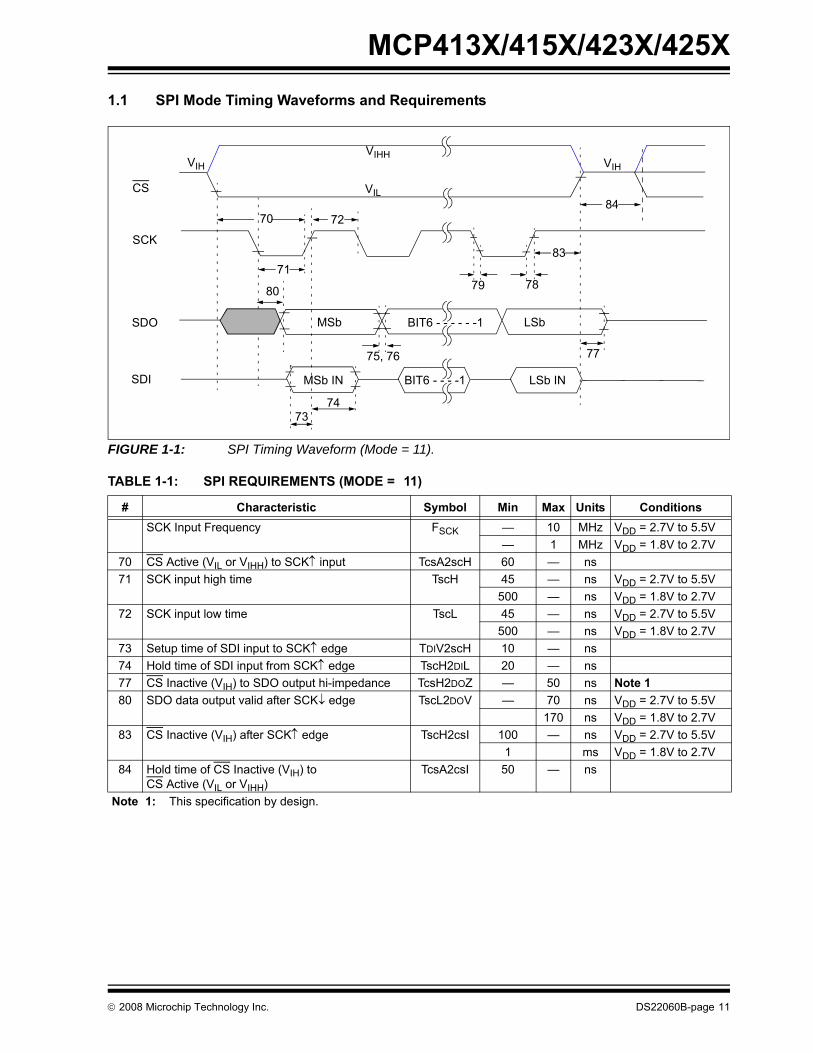
1.1 SPI Mode Timing Waveforms and RequirementsFIGURE 1-1: SPI Timing Waveform (Mode = 11).
TABLE 1-1: SPI REQUIREMENTS (MODE = 11) # Characteristic Symbol Min Max Units Conditions
SCK Input Frequency FSCK — 10 MHz VDD = 2.7V to 5.5V— 1 MHz VDD = 1.8V to 2.7V
70 CS Active (VIL or VIHH) to SCK↑ input TcsA2scH 60 — ns71 SCK input high time TscH 45 — ns VDD = 2.7V to 5.5V
500 — ns VDD = 1.8V to 2.7V72 SCK input low time TscL 45 — ns VDD = 2.7V to 5.5V
500 — ns VDD = 1.8V to 2.7V73 Setup time of SDI input to SCK↑ edge TDIV2scH 10 — ns74 Hold time of SDI input from SCK↑ edge TscH2DIL 20 — ns77 CS Inactive (VIH) to SDO output hi-impedance TcsH2DOZ — 50 ns Note 180 SDO data output valid after SCK↓ edge TscL2DOV — 70 ns VDD = 2.7V to 5.5V
170 ns VDD = 1.8V to 2.7V83 CS Inactive (VIH) after SCK↑ edge TscH2csI 100 — ns VDD = 2.7V to 5.5V
1 ms VDD = 1.8V to 2.7V84 Hold time of CS Inactive (VIH) to
CS Active (VIL or VIHH)TcsA2csI 50 — ns
Note 1: This specification by design.
CS
SCK
SDO
SDI
70
71
72
7374
75, 76 77
787980
MSb LSbBIT6 - - - - - -1
MSb IN BIT6 - - - -1 LSb IN
83
84
VIH
VIL
VIHH VIH
© 2008 Microchip Technology Inc. DS22060B-page 11
MCP413X/415X/423X/425X
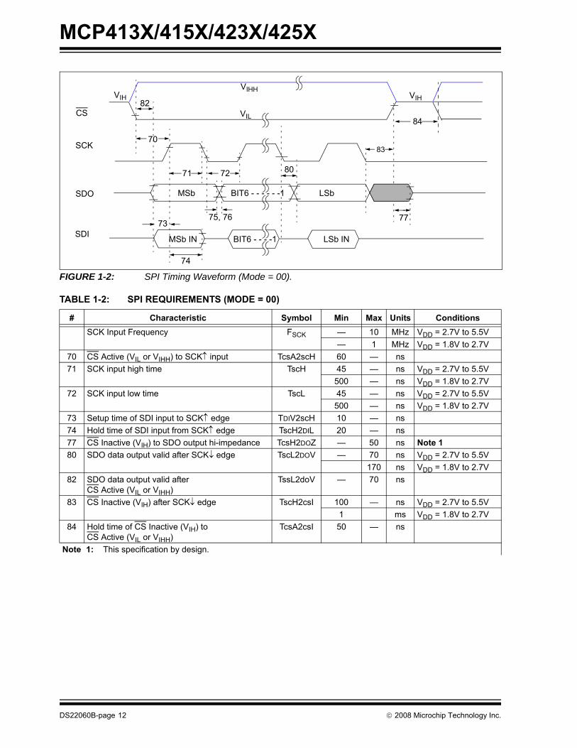
FIGURE 1-2: SPI Timing Waveform (Mode = 00).
TABLE 1-2: SPI REQUIREMENTS (MODE = 00)
# Characteristic Symbol Min Max Units ConditionsSCK Input Frequency FSCK — 10 MHz VDD = 2.7V to 5.5V
— 1 MHz VDD = 1.8V to 2.7V70 CS Active (VIL or VIHH) to SCK↑ input TcsA2scH 60 — ns71 SCK input high time TscH 45 — ns VDD = 2.7V to 5.5V
500 — ns VDD = 1.8V to 2.7V72 SCK input low time TscL 45 — ns VDD = 2.7V to 5.5V
500 — ns VDD = 1.8V to 2.7V73 Setup time of SDI input to SCK↑ edge TDIV2scH 10 — ns74 Hold time of SDI input from SCK↑ edge TscH2DIL 20 — ns77 CS Inactive (VIH) to SDO output hi-impedance TcsH2DOZ — 50 ns Note 180 SDO data output valid after SCK↓ edge TscL2DOV — 70 ns VDD = 2.7V to 5.5V
170 ns VDD = 1.8V to 2.7V82 SDO data output valid after
CS Active (VIL or VIHH)TssL2doV — 70 ns
83 CS Inactive (VIH) after SCK↓ edge TscH2csI 100 — ns VDD = 2.7V to 5.5V1 ms VDD = 1.8V to 2.7V
84 Hold time of CS Inactive (VIH) to CS Active (VIL or VIHH)
TcsA2csI 50 — ns
Note 1: This specification by design.
CS
SCK
SDO
SDI
70
71 72
82
74
75, 76
MSb BIT6 - - - - - -1 LSb
77
MSb IN BIT6 - - - -1 LSb IN
80
83
84
73
VIH
VIL
VIHH VIH
DS22060B-page 12 © 2008 Microchip Technology Inc.

MCP413X/415X/423X/425X
TABLE 1-3: SPI REQUIREMENTS FOR SDI/SDO MULTIPLEXED (READ OPERATION ONLY) (2)Characteristic Symbol Min Max Units ConditionsSCK Input Frequency FSCK — 250 kHz VDD = 2.7V to 5.5VCS Active (VIL or VIHH) to SCK↑ input TcsA2scH 60 — nsSCK input high time TscH 1.8 — usSCK input low time TscL 1.8 — nsSetup time of SDI input to SCK↑ edge TDIV2scH 40 — nsHold time of SDI input from SCK↑ edge TscH2DIL 40 — nsCS Inactive (VIH) to SDO output hi-impedance TcsH2DOZ — 50 ns Note 1SDO data output valid after SCK↓ edge TscL2DOV — 1.6 usSDO data output valid after CS Active (VIL or VIHH)
TssL2doV — 50 ns
CS Inactive (VIH) after SCK↓ edge TscH2csI 100 — nsHold time of CS Inactive (VIH) to CS Active (VIL or VIHH)
TcsA2csI 50 — ns
Note 1: This specification by design.2: This table is for the devices where the SPI’s SDI and SDO pins are multiplexed (SDI/SDO) and a Read
command is issued. This is NOT required for SDI/SDO operation with the Increment, Decrement, or Write commands. This data rate can be increased by having external pull-up resistors to increase the rising edges of each bit.
© 2008 Microchip Technology Inc. DS22060B-page 13
MCP413X/415X/423X/425X
TEMPERATURE CHARACTERISTICS Electrical Specifications: Unless otherwise indicated, VDD = +2.7V to +5.5V, VSS = GND.
Parameters Sym Min Typ Max Units Conditions
Temperature RangesSpecified Temperature Range TA -40 — +125 °COperating Temperature Range TA -40 — +125 °CStorage Temperature Range TA -65 — +150 °CThermal Package ResistancesThermal Resistance, 8L-DFN (3x3) θJA — 84.5 — °C/WThermal Resistance, 8L-MSOP θJA — 211 — °C/WThermal Resistance, 8L-PDIP θJA — 89.3 — °C/WThermal Resistance, 8L-SOIC θJA — 149.5 — °C/WThermal Resistance, 10L-DFN (3x3) θJA — 57 — °C/WThermal Resistance, 10L-MSOP θJA — 211 — °C/WThermal Resistance, 14L-PDIP θJA — 70 — °C/WThermal Resistance, 14L-SOIC θJA — 95.3 — °C/WThermal Resistance, 14L-TSSOP θJA — 100 — °C/WThermal Resistance, 16L-QFN θJA — 47 — °C/W
DS22060B-page 14 © 2008 Microchip Technology Inc.

MCP413X/415X/423X/425X
2.0 TYPICAL PERFORMANCE CURVES
Note: Unless otherwise indicated, TA = +25°C, VDD = 5V, VSS = 0V.
FIGURE 2-1: Device Current (IDD) vs. SPI Frequency (fSCK) and Ambient Temperature (VDD = 2.7V and 5.5V).
FIGURE 2-2: Device Current (ISHDN) and VDD. (CS = VDD) vs. Ambient Temperature.
FIGURE 2-3: CS Pull-up/Pull-down Resistance (RCS) and Current (ICS) vs. CS Input Voltage (VCS) (VDD = 5.5V).
FIGURE 2-4: CS High Input Entry/Exit Threshold vs. Ambient Temperature and VDD.
Note: The graphs and tables provided following this note are a statistical summary based on a limited number ofsamples and are provided for informational purposes only. The performance characteristics listed hereinare not tested or guaranteed. In some graphs or tables, the data presented may be outside the specifiedoperating range (e.g., outside specified power supply range) and therefore outside the warranted range.
050
100150200250300350400450500550600650
0.00 2.00 4.00 6.00 8.00 10.00 12.00fSCK (MHz)
Ope
ratin
g C
urre
nt (I
DD) (
µA) 2.7V -40°C
2.7V 25°C2.7V 85°C2.7V 125°C5.5V -40°C5.5V 25°C5.5V 85°C5.5V 125°C
0.0
0.5
1.0
1.5
2.0
2.5
3.0
-40 25 85 125Ambient Temperature (°C)
Stan
dby
Cur
rent
(Ist
by) (
µA)
5.5V
2.7V
0
50
100
150
200
250
2 3 4 5 6 7 8 9 10VCS (V)
RC
S (k
Ohm
s)
-1000-800-600-400-20002004006008001000
I CS (µ
A)ICS
RCS
0
2
4
6
8
10
12
-40 -20 0 20 40 60 80 100 120Ambient Temperature (°C)
CS
VPP
Thr
esho
ld (V
)
2.7V Exit
5.5V Exit
2.7V Entry5.5V Entry
© 2008 Microchip Technology Inc. DS22060B-page 15

MCP413X/415X/423X/425X
Note: Unless otherwise indicated, TA = +25°C, VDD = 5V, VSS = 0V.FIGURE 2-5: 5 kΩ Pot Mode – RW (Ω), INL (LSb), DNL (LSb) vs. Wiper Setting and Ambient Temperature (VDD = 5.5V).
FIGURE 2-6: 5 kΩ Pot Mode – RW (Ω), INL (LSb), DNL (LSb) vs. Wiper Setting and Ambient Temperature (VDD = 3.0V).
FIGURE 2-7: 5 kΩ Pot Mode – RW (Ω), INL (LSb), DNL (LSb) vs. Wiper Setting and Ambient Temperature (VDD = 1.8V).
FIGURE 2-8: 5 kΩ Rheo Mode – RW (Ω), INL (LSb), DNL (LSb) vs. Wiper Setting and Ambient Temperature (VDD = 5.5V).
FIGURE 2-9: 5 kΩ Rheo Mode – RW (Ω), INL (LSb), DNL (LSb) vs. Wiper Setting and Ambient Temperature (VDD = 3.0V).
FIGURE 2-10: 5 kΩ Rheo Mode – RW (Ω), INL (LSb), DNL (LSb) vs. Wiper Setting and Ambient Temperature (VDD = 1.8V).
20
40
60
80
100
120
0 32 64 96 128 160 192 224 256Wiper Setting (decimal)
Wip
er R
esis
tanc
e (R
W)
(ohm
s)
-0.3
-0.2
-0.1
0
0.1
0.2
0.3
Erro
r (LS
b)
-40C Rw 25C Rw 85C Rw 125C Rw-40C INL 25C INL 85C INL 125C INL-40C DNL 25C DNL 85C DNL 125C DNL
INLDNL
RW-40°C 25°C85°C125°C
20
60
100
140
180
220
260
300
0 32 64 96 128 160 192 224 256Wiper Setting (decimal)
Wip
er R
esis
tanc
e (R
W)
(ohm
s)
-0.3
-0.2
-0.1
0
0.1
0.2
0.3
Erro
r (LS
b)
-40C Rw 25C Rw 85C Rw 125C Rw-40C INL 25C INL 85C INL 125C INL-40C DNL 25C DNL 85C DNL 125C DNL
INLDNL
-40°C 25°C85°C
RW
125°C
0
500
1000
1500
2000
2500
0 64 128 192 256Wiper Setting (decimal)
Wip
er R
esis
tanc
e (R
W)
(ohm
s)
-0.3
-0.2-0.100.1
0.20.30.40.5
Erro
r (LS
b)
-40C Rw 25C Rw 85C Rw 125C Rw-40C INL 25C INL 85C INL 125C INL-40C DNL 25C DNL 85C DNL 125C DNL
INL
DNLRW
Note: Refer to AN1080 for additional informa-tion on the characteristics of the wiperresistance (RW) with respect to devicevoltage and wiper setting value.
20
40
60
80
100
120
0 32 64 96 128 160 192 224 256Wiper Setting (decimal)
Wip
er R
esis
tanc
e (R
W)
(ohm
s)
-1.25
-0.75
-0.25
0.25
0.75
1.25
Erro
r (LS
b)
-40C Rw 25C Rw 85C Rw 125C Rw-40C INL 25C INL 85C INL 125C INL-40C DNL 25C DNL 85C DNL 125C DNL
INL
DNL
RW
-40°C25°C85°C125°C
20
60
100
140
180
220
260
300
0 32 64 96 128 160 192 224 256Wiper Setting (decimal)
Wip
er R
esis
tanc
e (R
W)
(ohm
s)
-2
0
2
4
6
Erro
r (LS
b)
-40C Rw 25C Rw 85C Rw 125C Rw-40C INL 25C INL 85C INL 125C INL-40C DNL 25C DNL 85C DNL 125C DNL
INL
DNL
RW
-40°C25°C
85°C125°C
0
500
1000
1500
2000
2500
0 64 128 192 256Wiper Setting (decimal)
Wip
er R
esis
tanc
e (R
W)
(ohm
s)
-2
18
38
58
78
98
118
Erro
r (LS
b)
-40C Rw 25C Rw 85C Rw 125C Rw-40C INL 25C INL 85C INL 125C INL-40C DNL 25C DNL 85C DNL 125C DNL
INL
DNLRW
Note: Refer to AN1080 for additional informa-tion on the characteristics of the wiperresistance (RW) with respect to devicevoltage and wiper setting value.
DS22060B-page 16 © 2008 Microchip Technology Inc.

MCP413X/415X/423X/425X
Note: Unless otherwise indicated, TA = +25°C, VDD = 5V, VSS = 0V.FIGURE 2-11: 5 kΩ – Nominal Resistance (Ω) vs. Ambient Temperature and VDD.
FIGURE 2-12: 5 kΩ – RWB (Ω) vs. Wiper Setting and Ambient Temperature.
5050
5100
5150
5200
5250
5300
-40 0 40 80 120Ambient Temperature (°C)
Nom
inal
Res
ista
nce
(RA
B)
(Ohm
s)
2.7V
5.5V
1.8V
0
1000
2000
3000
4000
5000
6000
0 32 64 96 128 160 192 224 256Wiper Setting (decimal)
RW
B (O
hms)
-40°C25°C85°C125°C
© 2008 Microchip Technology Inc. DS22060B-page 17

MCP413X/415X/423X/425X
Note: Unless otherwise indicated, TA = +25°C, VDD = 5V, VSS = 0V.FIGURE 2-13: 5 kΩ – Low-Voltage Decrement Wiper Settling Time (VDD = 5.5V) (1 µs/Div).
FIGURE 2-14: 5 kΩ – Low-Voltage Decrement Wiper Settling Time (VDD = 2.7V) (1 µs/Div).
FIGURE 2-15: 5 kΩ – Power-Up Wiper Response Time (20 ms/Div).
FIGURE 2-16: 5 kΩ – Low-Voltage Increment Wiper Settling Time (VDD = 5.5V) (1 µs/Div).
FIGURE 2-17: 5 kΩ – Low-Voltage Increment Wiper Settling Time (VDD = 2.7V) (1 µs/Div).
DS22060B-page 18 © 2008 Microchip Technology Inc.
MCP413X/415X/423X/425X
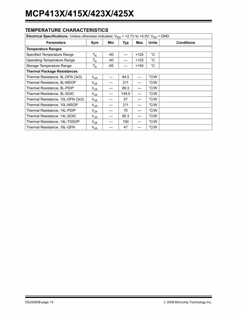
Note: Unless otherwise indicated, TA = +25°C, VDD = 5V, VSS = 0V.FIGURE 2-18: 10 kΩ Pot Mode – RW (Ω), INL (LSb), DNL (LSb) vs. Wiper Setting and Ambient Temperature (VDD = 5.5V).
FIGURE 2-19: 10 kΩ Pot Mode – RW (Ω), INL (LSb), DNL (LSb) vs. Wiper Setting and Ambient Temperature (VDD = 3.0V).
FIGURE 2-20: 10 kΩ Pot Mode – RW (Ω), INL (LSb), DNL (LSb) vs. Wiper Setting and Ambient Temperature (VDD = 1.8V).
FIGURE 2-21: 10 kΩ Rheo Mode – RW (Ω), INL (LSb), DNL (LSb) vs. Wiper Setting and Ambient Temperature (VDD = 5.5V).
FIGURE 2-22: 10 kΩ Rheo Mode – RW (Ω), INL (LSb), DNL (LSb) vs. Wiper Setting and Ambient Temperature (VDD = 3.0V).
FIGURE 2-23: 10 kΩ Rheo Mode – RW (Ω), INL (LSb), DNL (LSb) vs. Wiper Setting and Ambient Temperature (VDD = 1.8V).
20
40
60
80
100
120
0 25 50 75 100 125 150 175 200 225 250Wiper Setting (decimal)
Wip
er R
esis
tanc
e (R
W)
(ohm
s)
-0.3
-0.2
-0.1
0
0.1
0.2
0.3
Erro
r (LS
b)
-40C Rw 25C Rw 85C Rw 125C Rw-40C INL 25C INL 85C INL 125C INL-40C DNL 25C DNL 85C DNL 125C DNL
INLDNL
RW-40°C25°C
85°C125°C
20
60
100
140
180
220
260
300
0 32 64 96 128 160 192 224 256Wiper Setting (decimal)
Wip
er R
esis
tanc
e (R
W)
(ohm
s)
-0.3
-0.2
-0.1
0
0.1
0.2
0.3
Erro
r (LS
b)
-40C Rw 25C Rw 85C Rw 125C Rw-40C INL 25C INL 85C INL 125C INL-40C DNL 25C DNL 85C DNL 125C DNL
INLDNL
RW
-40°C25°C85°C125°C
0500
1000150020002500300035004000
0 64 128 192 256Wiper Setting (decimal)
Wip
er R
esis
tanc
e (R
W)(o
hms)
-0.3-0.2-0.100.10.20.30.40.50.6
Erro
r (LS
b)
-40C Rw 25C Rw 85C Rw 125C Rw-40C INL 25C INL 85C INL 125C INL-40C DNL 25C DNL 85C DNL 125C DNL
INL
DNL
RW
Note: Refer to AN1080 for additional informa-tion on the characteristics of the wiperresistance (RW) with respect to devicevoltage and wiper setting value.
20
40
60
80
100
120
0 32 64 96 128 160 192 224 256Wiper Setting (decimal)
Wip
er R
esis
tanc
e (R
W)
(ohm
s)
-1
-0.5
0
0.5
1
Erro
r (LS
b)
-40C Rw 25C Rw 85C Rw 125C Rw-40C INL 25C INL 85C INL 125C INL-40C DNL 25C DNL 85C DNL 125C DNL
INL
DNLRW-40°C25°C85°C125°C
20
60
100
140
180
220
260
300
0 25 50 75 100 125 150 175 200 225 250Wiper Setting (decimal)
Wip
er R
esis
tanc
e (R
W)
(ohm
s)
-2
-1
0
1
2
3
4
Erro
r (LS
b)
-40C Rw 25C Rw 85C Rw 125C Rw-40C INL 25C INL 85C INL 125C INL-40C DNL 25C DNL 85C DNL 125C DNL
INL
DNL RW-40°C25°C85°C125°C
0500
1000150020002500300035004000
0 64 128 192 256Wiper Setting (decimal)
Wip
er R
esis
tanc
e (R
W)
(ohm
s)
-28182838485868788898
Erro
r (LS
b)
-40C Rw 25C Rw 85C Rw 125C Rw-40C INL 25C INL 85C INL 125C INL-40C DNL 25C DNL 85C DNL 125C DNL
INL
DNLRW
Note: Refer to AN1080 for additional informa-tion on the characteristics of the wiperresistance (RW) with respect to devicevoltage and wiper setting value.
© 2008 Microchip Technology Inc. DS22060B-page 19
MCP413X/415X/423X/425X
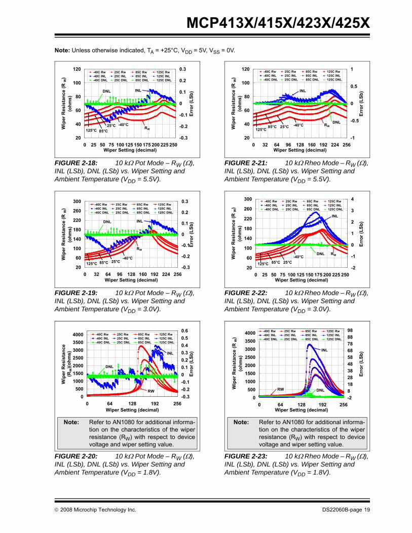
Note: Unless otherwise indicated, TA = +25°C, VDD = 5V, VSS = 0V.FIGURE 2-24: 10 kΩ – Nominal Resistance (Ω) vs. Ambient Temperature and VDD.
FIGURE 2-25: 10 kΩ – RWB (Ω) vs. Wiper Setting and Ambient Temperature.
985099009950
10000100501010010150102001025010300
-40 0 40 80 120Ambient Temperature (°C)
Nom
inal
Res
ista
nce
(RA
B)
(Ohm
s)
2.7V
5.5V
1.8V
0
2000
4000
6000
8000
10000
12000
0 32 64 96 128 160 192 224 256Wiper Setting (decimal)
RW
B (O
hms)
-40°C25°C85°C125°C
DS22060B-page 20 © 2008 Microchip Technology Inc.
MCP413X/415X/423X/425X
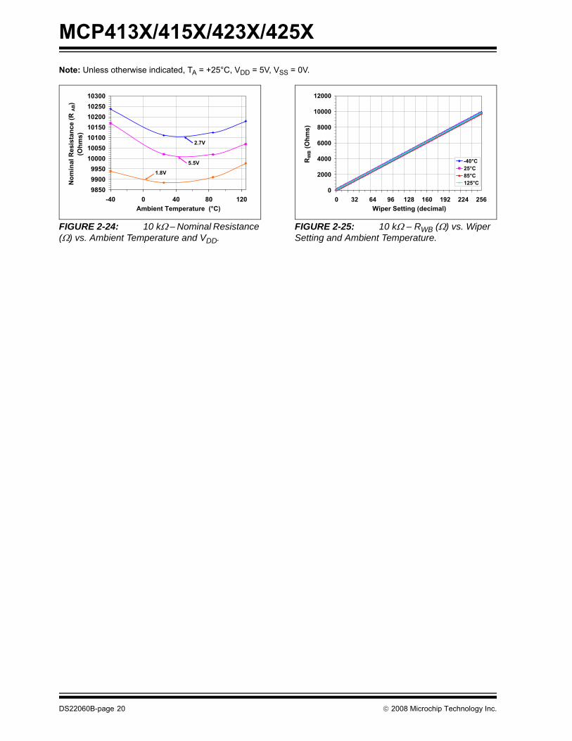
Note: Unless otherwise indicated, TA = +25°C, VDD = 5V, VSS = 0V.FIGURE 2-26: 10 kΩ – Low-Voltage Decrement Wiper Settling Time (VDD = 5.5V) (1 µs/Div).
FIGURE 2-27: 10 kΩ – Low-Voltage Decrement Wiper Settling Time (VDD = 2.7V) (1 µs/Div).
FIGURE 2-28: 10 kΩ – Low-Voltage Increment Wiper Settling Time (VDD = 5.5V) (1 µs/Div).
FIGURE 2-29: 10 kΩ – Low-Voltage Increment Wiper Settling Time (VDD = 2.7V) (1 µs/Div).
© 2008 Microchip Technology Inc. DS22060B-page 21
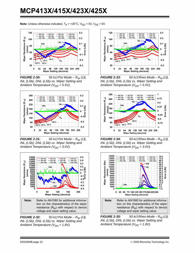
MCP413X/415X/423X/425X
Note: Unless otherwise indicated, TA = +25°C, VDD = 5V, VSS = 0V.FIGURE 2-30: 50 kΩ Pot Mode – RW (Ω), INL (LSb), DNL (LSb) vs. Wiper Setting and Ambient Temperature (VDD = 5.5V).
FIGURE 2-31: 50 kΩ Pot Mode – RW (Ω), INL (LSb), DNL (LSb) vs. Wiper Setting and Ambient Temperature (VDD = 3.0V).
FIGURE 2-32: 50 kΩ Pot Mode – RW (Ω), INL (LSb), DNL (LSb) vs. Wiper Setting and Ambient Temperature (VDD = 1.8V).
FIGURE 2-33: 50 kΩ Rheo Mode – RW (Ω), INL (LSb), DNL (LSb) vs. Wiper Setting and Ambient Temperature (VDD = 5.5V).
FIGURE 2-34: 50 kΩ Rheo Mode – RW (Ω), INL (LSb), DNL (LSb) vs. Wiper Setting and Ambient Temperature (VDD = 3.0V).
FIGURE 2-35: 50 kΩ Rheo Mode – RW (Ω), INL (LSb), DNL (LSb) vs. Wiper Setting and Ambient Temperature (VDD = 1.8V).
20
40
60
80
100
120
0 32 64 96 128 160 192 224 256Wiper Setting (decimal)
Wip
er R
esis
tanc
e (R
W)
(ohm
s)
-0.3
-0.2
-0.1
0
0.1
0.2
0.3
Erro
r (LS
b)
-40C Rw 25C Rw 85C Rw 125C Rw-40C INL 25C INL 85C INL 125C INL-40C DNL 25C DNL 85C DNL 125C DNL
INLDNL
RW-40°C
25°C85°C125°C
20
60
100
140
180
220
260
300
0 32 64 96 128 160 192 224 256Wiper Setting (decimal)
Wip
er R
esis
tanc
e (R
W)
(ohm
s)
-0.3
-0.2
-0.1
0
0.1
0.2
0.3
Erro
r (LS
b)
-40C Rw 25C Rw 85C Rw 125C Rw-40C INL 25C INL 85C INL 125C INL-40C DNL 25C DNL 85C DNL 125C DNL
INLDNL
RW
-40°C25°C85°C125°C
0100020003000400050006000700080009000
100001100012000130001400015000
0 64 128 192 256Wiper Setting (decimal)
Wip
er R
esis
tanc
e (R
W)
(ohm
s)
-0.5-0.4-0.3-0.2-0.100.10.20.30.40.5
Erro
r (LS
b)
-40C Rw 25C Rw 85C Rw 125C Rw-40C INL 25C INL 85C INL 125C INL-40C DNL 25C DNL 85C DNL 125C DNL
INL
DNL
RW
Note: Refer to AN1080 for additional informa-tion on the characteristics of the wiperresistance (RW) with respect to devicevoltage and wiper setting value.
20
40
60
80
100
120
0 32 64 96 128 160 192 224 256Wiper Setting (decimal)
Wip
er R
esis
tanc
e (R
W)
(ohm
s)
-0.3
-0.2
-0.1
0
0.1
0.2
0.3
Erro
r (LS
b)
-40C Rw 25C Rw 85C Rw 125C Rw-40C INL 25C INL 85C INL 125C INL-40C DNL 25C DNL 85C DNL 125C DNL
INLDNL
RW-40°C25°C85°C125°C
20
60
100
140
180
220
260
300
0 32 64 96 128 160 192 224 256Wiper Setting (decimal)
Wip
er R
esis
tanc
e (R
W)
(ohm
s)
-1
-0.75
-0.5
-0.25
0
0.25
0.5
0.75
1
Erro
r (LS
b)
-40C Rw 25C Rw 85C Rw 125C Rw-40C INL 25C INL 85C INL 125C INL-40C DNL 25C DNL 85C DNL 125C DNL
INL
DNL
RW
-40°C25°C85°C125°C
0100020003000400050006000700080009000
100001100012000130001400015000
0 25 50 75 100125150175200225250Wiper Setting (decimal)
Wip
er R
esis
tanc
e (R
w)
(ohm
s)
-1.53.58.513.518.523.528.533.538.543.548.553.558.563.568.573.578.5
Erro
r (LS
b)
-40C Rw 25C Rw 85C Rw 125C Rw-40C INL 25C INL 85C INL 125C INL-40C DNL 25C DNL 85C DNL 125C DNL
INL
DNL
RW
Note: Refer to AN1080 for additional informa-tion on the characteristics of the wiperresistance (RW) with respect to devicevoltage and wiper setting value.
DS22060B-page 22 © 2008 Microchip Technology Inc.

MCP413X/415X/423X/425X
Note: Unless otherwise indicated, TA = +25°C, VDD = 5V, VSS = 0V.FIGURE 2-36: 50 kΩ – Nominal Resistance (Ω) vs. Ambient Temperature and VDD.
FIGURE 2-37: 50 kΩ – RWB (Ω) vs. Wiper Setting and Ambient Temperature.
49000
49500
50000
50500
51000
51500
52000
52500
-40 0 40 80 120Ambient Temperature (°C)
Nom
inal
Res
ista
nce
(RA
B)
(Ohm
s)
2.7V
1.8V
5.5V
0
10000
20000
30000
40000
50000
60000
0 32 64 96 128 160 192 224 256Wiper Setting (decimal)
RW
B (O
hms)
-40°C25°C85°C125°C
© 2008 Microchip Technology Inc. DS22060B-page 23

MCP413X/415X/423X/425X
Note: Unless otherwise indicated, TA = +25°C, VDD = 5V, VSS = 0V.FIGURE 2-38: 50 kΩ – Low-Voltage Decrement Wiper Settling Time (VDD = 5.5V) (1 µs/Div).
FIGURE 2-39: 50 kΩ – Low-Voltage Decrement Wiper Settling Time (VDD = 2.7V) (1 µs/Div).
FIGURE 2-40: 50 kΩ – Low-Voltage Increment Wiper Settling Time (VDD = 5.5V) (1 µs/Div).
FIGURE 2-41: 50 kΩ – Low-Voltage Increment Wiper Settling Time (VDD = 2.7V) (1 µs/Div).
DS22060B-page 24 © 2008 Microchip Technology Inc.

MCP413X/415X/423X/425X
Note: Unless otherwise indicated, TA = +25°C, VDD = 5V, VSS = 0V.FIGURE 2-42: 100 kΩ Pot Mode – RW (Ω), INL (LSb), DNL (LSb) vs. Wiper Setting and Ambient Temperature (VDD = 5.5V).
FIGURE 2-43: 100 kΩ Pot Mode – RW (Ω), INL (LSb), DNL (LSb) vs. Wiper Setting and Ambient Temperature (VDD = 3.0V).
FIGURE 2-44: 100 kΩ Pot Mode – RW (Ω), INL (LSb), DNL (LSb) vs. Wiper Setting and Ambient Temperature (VDD = 1.8V).
FIGURE 2-45: 100 kΩ Rheo Mode – RW (Ω), INL (LSb), DNL (LSb) vs. Wiper Setting and Ambient Temperature (VDD = 5.5V).
FIGURE 2-46: 100 kΩ Rheo Mode – RW (Ω), INL (LSb), DNL (LSb) vs. Wiper Setting and Ambient Temperature (VDD = 3.0V).
FIGURE 2-47: 100 kΩ Rheo Mode – RW (Ω), INL (LSb), DNL (LSb) vs. Wiper Setting and Ambient Temperature (VDD = 1.8V).
20
40
60
80
100
120
0 32 64 96 128 160 192 224 256Wiper Setting (decimal)
Wip
er R
esis
tanc
e (R
W)
(ohm
s)
-0.2
-0.1
0
0.1
0.2
Erro
r (LS
b)
-40C Rw 25C Rw 85C Rw 125C Rw-40C INL 25C INL 85C INL 125C INL-40C DNL 25C DNL 85C DNL 125C DNL
INLDNL
RW-40°C25°C
85°C125°C
20
60
100
140
180
220
260
300
0 32 64 96 128 160 192 224 256Wiper Setting (decimal)
Wip
er R
esis
tanc
e (R
W)
(ohm
s)
-0.2-0.15-0.1-0.050
0.050.10.150.2
Erro
r (LS
b)
-40C Rw 25C Rw 85C Rw 125C Rw-40C INL 25C INL 85C INL 125C INL-40C DNL 25C DNL 85C DNL 125C DNL
INLDNL
RW
-40°C25°C85°C125°C
0
5000
10000
15000
20000
25000
0 64 128 192 256Wiper Setting (decimal)
Wip
er R
esis
tanc
e (R
W)
(ohm
s)
-0.35
-0.25
-0.15
-0.05
0.05
0.15
0.25
0.35
Erro
r (LS
b)
-40C Rw 25C Rw 85C Rw 125C Rw-40C INL 25C INL 85C INL 125C INL-40C DNL 25C DNL 85C DNL 125C DNL
INL
DNL
RW
Note: Refer to AN1080 for additional informa-tion on the characteristics of the wiperresistance (RW) with respect to devicevoltage and wiper setting value.
20
40
60
80
100
120
0 32 64 96 128 160 192 224 256Wiper Setting (decimal)
Wip
er R
esis
tanc
e (R
W)
(ohm
s)
-0.3
-0.2
-0.1
0
0.1
0.2
0.3
Erro
r (LS
b)
-40C Rw 25C Rw 85C Rw 125C Rw-40C INL 25C INL 85C INL 125C INL-40C DNL 25C DNL 85C DNL 125C DNL
INL
DNL
RW-40°C25°C85°C125°C
20
60
100
140
180
220
260
300
0 32 64 96 128 160 192 224 256Wiper Setting (decimal)
Wip
er R
esis
tanc
e (R
w)
(ohm
s)
-0.6
-0.4
-0.2
0
0.2
0.4
0.6
Erro
r (LS
b)
-40C Rw 25C Rw 85C Rw 125C Rw-40C INL 25C INL 85C INL 125C INL-40C DNL 25C DNL 85C DNL 125C DNL
INL
DNL
RW
-40°C25°C85°C125°C
0
5000
10000
15000
20000
25000
0 64 128 192 256Wiper Setting (decimal)
Wip
er R
esis
tanc
e (R
W)
(ohm
s)
-14914192429343944495459
Erro
r (LS
b)
-40C Rw 25C Rw 85C Rw 125C Rw-40C INL 25C INL 85C INL 125C INL-40C DNL 25C DNL 85C DNL 125C DNL
INL
DNL
RW
Note: Refer to AN1080 for additional informa-tion on the characteristics of the wiperresistance (RW) with respect to devicevoltage and wiper setting value.
© 2008 Microchip Technology Inc. DS22060B-page 25
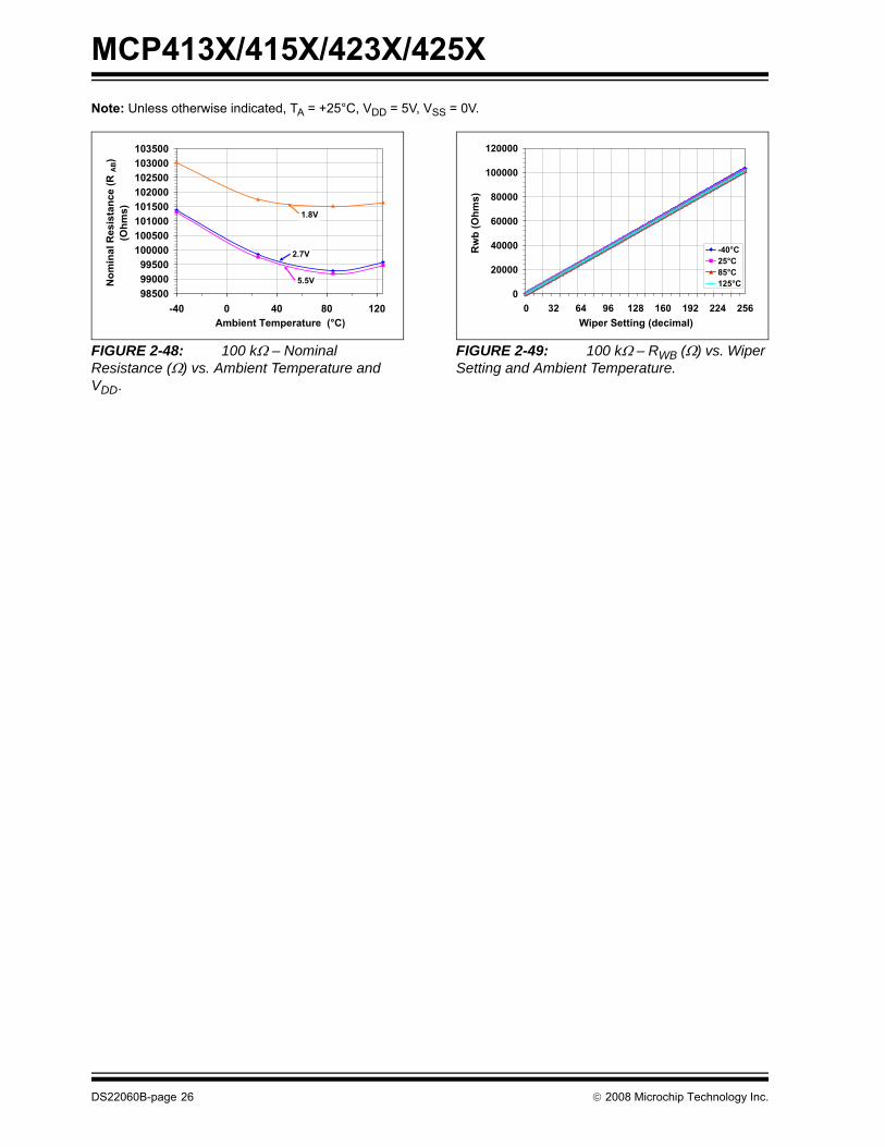
MCP413X/415X/423X/425X
Note: Unless otherwise indicated, TA = +25°C, VDD = 5V, VSS = 0V.FIGURE 2-48: 100 kΩ – Nominal Resistance (Ω) vs. Ambient Temperature and VDD.
FIGURE 2-49: 100 kΩ – RWB (Ω) vs. Wiper Setting and Ambient Temperature.
985009900099500
100000100500101000101500102000102500103000103500
-40 0 40 80 120Ambient Temperature (°C)
Nom
inal
Res
ista
nce
(RA
B)
(Ohm
s)
2.7V
5.5V
1.8V
0
20000
40000
60000
80000
100000
120000
0 32 64 96 128 160 192 224 256Wiper Setting (decimal)
Rw
b (O
hms)
-40°C25°C85°C125°C
DS22060B-page 26 © 2008 Microchip Technology Inc.

MCP413X/415X/423X/425X
Note: Unless otherwise indicated, TA = +25°C, VDD = 5V, VSS = 0V.FIGURE 2-50: 100 kΩ – Low-Voltage Decrement Wiper Settling Time (VDD = 5.5V) (1 µs/Div).
FIGURE 2-51: 100 kΩ – Low-Voltage Decrement Wiper Settling Time (VDD = 2.7V) (1 µs/Div).
FIGURE 2-52: 100 kΩ – Low-Voltage Increment Wiper Settling Time (VDD = 2.7V) (1 µs/Div).
FIGURE 2-53: 100 kΩ – Power-Up Wiper Response Time (1 µs/Div).
© 2008 Microchip Technology Inc. DS22060B-page 27
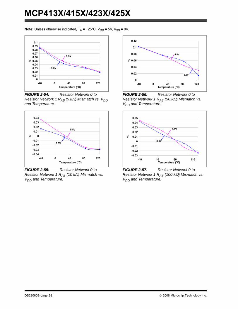
MCP413X/415X/423X/425X
Note: Unless otherwise indicated, TA = +25°C, VDD = 5V, VSS = 0V.FIGURE 2-54: Resistor Network 0 to Resistor Network 1 RAB (5 kΩ) Mismatch vs. VDD and Temperature.
FIGURE 2-55: Resistor Network 0 to Resistor Network 1 RAB (10 kΩ) Mismatch vs. VDD and Temperature.
FIGURE 2-56: Resistor Network 0 to Resistor Network 1 RAB (50 kΩ) Mismatch vs. VDD and Temperature.
FIGURE 2-57: Resistor Network 0 to Resistor Network 1 RAB (100 kΩ) Mismatch vs. VDD and Temperature.
00.010.020.030.040.050.060.070.080.090.1
-40 0 40 80 120Temperature (°C)
%
5.5V
3.0V
-0.04-0.03-0.02-0.01
00.010.020.030.04
-40 0 40 80 120Temperature (°C)
%
5.5V
3.0V
0
0.02
0.04
0.06
0.08
0.1
0.12
-40 0 40 80 120Temperature (°C)
%
5.5V
3.0V
-0.03-0.02-0.01
00.010.020.030.040.05
-40 10 60 110Temperature (°C)
%5.5V
3.0V
DS22060B-page 28 © 2008 Microchip Technology Inc.
MCP413X/415X/423X/425X
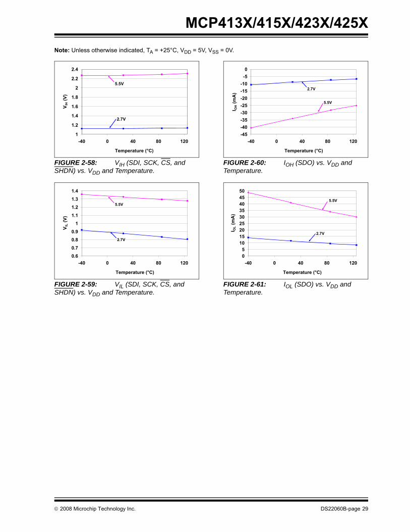
Note: Unless otherwise indicated, TA = +25°C, VDD = 5V, VSS = 0V.FIGURE 2-58: VIH (SDI, SCK, CS, and SHDN) vs. VDD and Temperature.
FIGURE 2-59: VIL (SDI, SCK, CS, and SHDN) vs. VDD and Temperature.
FIGURE 2-60: IOH (SDO) vs. VDD and Temperature.
FIGURE 2-61: IOL (SDO) vs. VDD and Temperature.
1
1.2
1.4
1.6
1.8
2
2.2
2.4
-40 0 40 80 120
Temperature (°C)
V IH (V
)
5.5V
2.7V
0.60.70.80.9
11.11.21.31.4
-40 0 40 80 120
Temperature (°C)
V IL
(V)
5.5V
2.7V
-45-40-35-30-25-20-15-10-50
-40 0 40 80 120
Temperature (°C)
I OH (m
A)
5.5V
2.7V
05
101520253035404550
-40 0 40 80 120
Temperature (°C)
I OL
(mA
)
5.5V
2.7V
© 2008 Microchip Technology Inc. DS22060B-page 29
MCP413X/415X/423X/425X
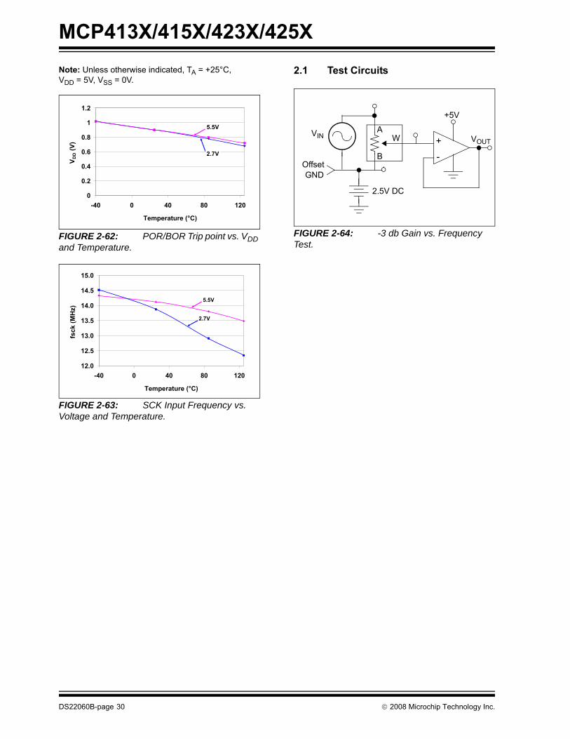
Note: Unless otherwise indicated, TA = +25°C,VDD = 5V, VSS = 0V.FIGURE 2-62: POR/BOR Trip point vs. VDD and Temperature.
FIGURE 2-63: SCK Input Frequency vs. Voltage and Temperature.
2.1 Test Circuits
FIGURE 2-64: -3 db Gain vs. Frequency Test.
0
0.2
0.4
0.6
0.8
1
1.2
-40 0 40 80 120
Temperature (°C)
V DD (V
)
2.7V
5.5V
12.0
12.5
13.0
13.5
14.0
14.5
15.0
-40 0 40 80 120
Temperature (°C)
fsck
(MH
z)
2.7V
5.5V
+
-
VOUT
2.5V DC
+5V
A
B
W
OffsetGND
VIN
DS22060B-page 30 © 2008 Microchip Technology Inc.
MCP413X/415X/423X/425X
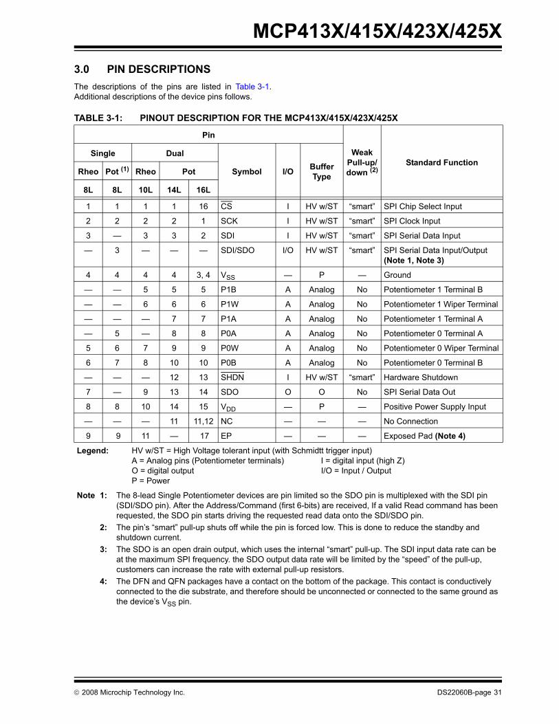
3.0 PIN DESCRIPTIONSThe descriptions of the pins are listed in Table 3-1.Additional descriptions of the device pins follows.
TABLE 3-1: PINOUT DESCRIPTION FOR THE MCP413X/415X/423X/425X
Pin
Weak Pull-up/down (2)
Standard FunctionSingle Dual
Symbol I/O Buffer TypeRheo Pot (1) Rheo Pot
8L 8L 10L 14L 16L
1 1 1 1 16 CS I HV w/ST “smart” SPI Chip Select Input
2 2 2 2 1 SCK I HV w/ST “smart” SPI Clock Input
3 — 3 3 2 SDI I HV w/ST “smart” SPI Serial Data Input
— 3 — — — SDI/SDO I/O HV w/ST “smart” SPI Serial Data Input/Output (Note 1, Note 3)
4 4 4 4 3, 4 VSS — P — Ground
— — 5 5 5 P1B A Analog No Potentiometer 1 Terminal B
— — 6 6 6 P1W A Analog No Potentiometer 1 Wiper Terminal
— — — 7 7 P1A A Analog No Potentiometer 1 Terminal A
— 5 — 8 8 P0A A Analog No Potentiometer 0 Terminal A
5 6 7 9 9 P0W A Analog No Potentiometer 0 Wiper Terminal
6 7 8 10 10 P0B A Analog No Potentiometer 0 Terminal B
— — — 12 13 SHDN I HV w/ST “smart” Hardware Shutdown
7 — 9 13 14 SDO O O No SPI Serial Data Out
8 8 10 14 15 VDD — P — Positive Power Supply Input
— — — 11 11,12 NC — — — No Connection
9 9 11 — 17 EP — — — Exposed Pad (Note 4)
Legend: HV w/ST = High Voltage tolerant input (with Schmidtt trigger input) A = Analog pins (Potentiometer terminals) I = digital input (high Z) O = digital output I/O = Input / Output P = Power
Note 1: The 8-lead Single Potentiometer devices are pin limited so the SDO pin is multiplexed with the SDI pin (SDI/SDO pin). After the Address/Command (first 6-bits) are received, If a valid Read command has been requested, the SDO pin starts driving the requested read data onto the SDI/SDO pin.
2: The pin’s “smart” pull-up shuts off while the pin is forced low. This is done to reduce the standby and shutdown current.
3: The SDO is an open drain output, which uses the internal “smart” pull-up. The SDI input data rate can be at the maximum SPI frequency. the SDO output data rate will be limited by the “speed” of the pull-up, customers can increase the rate with external pull-up resistors.
4: The DFN and QFN packages have a contact on the bottom of the package. This contact is conductively connected to the die substrate, and therefore should be unconnected or connected to the same ground as the device’s VSS pin.
© 2008 Microchip Technology Inc. DS22060B-page 31

MCP413X/415X/423X/425X
3.1 Chip Select (CS)The CS pin is the serial interface’s chip select input.Forcing the CS pin to VIL enables the serial commands.Forcing the CS pin to VIHH enables the high-voltageserial commands.3.2 Serial Data In (SDI) The SDI pin is the serial interfaces Serial Data In pin.This pin is connected to the Host Controllers SDO pin.
3.3 Serial Data In / Serial Data Out (SDI/SDO)
On the MCP41X1 devices, pin-out limitations do notallow for individual SDI and SDO pins. On thesedevices, the SDI and SDO pins are multiplexed.
The MCP41X1 serial interface knows when the pinneeds to change from being an input (SDI) to being anoutput (SDO). The Host Controller’s SDO pin must beproperly protected from a drive conflict.
3.4 Ground (VSS)The VSS pin is the device ground reference.
3.5 Potentiometer Terminal BThe terminal B pin is connected to the internalpotentiometer’s terminal B.
The potentiometer’s terminal B is the fixed connectionto the Zero Scale wiper value of the digitalpotentiometer. This corresponds to a wiper value of0x00 for both 7-bit and 8-bit devices.
The terminal B pin does not have a polarity relative tothe terminal W or A pins. The terminal B pin cansupport both positive and negative current. The voltageon terminal B must be between VSS and VDD.
MCP42XX devices have two terminal B pins, one foreach resistor network.
3.6 Potentiometer Wiper (W) Terminal The terminal W pin is connected to the internalpotentiometer’s terminal W (the wiper). The wiperterminal is the adjustable terminal of the digitalpotentiometer. The terminal W pin does not have apolarity relative to terminals A or B pins. The terminalW pin can support both positive and negative current.The voltage on terminal W must be between VSS andVDD.
MCP42XX devices have two terminal W pins, one foreach resistor network.
3.7 Potentiometer Terminal AThe terminal A pin is available on the MCP4XX1devices, and is connected to the internalpotentiometer’s terminal A.
The potentiometer’s terminal A is the fixed connectionto the Full-Scale wiper value of the digitalpotentiometer. This corresponds to a wiper value of0x100 for 8-bit devices or 0x80 for 7-bit devices.
The terminal A pin does not have a polarity relative tothe terminal W or B pins. The terminal A pin cansupport both positive and negative current. The voltageon terminal A must be between VSS and VDD.
The terminal A pin is not available on the MCP4XX2devices, and the internally terminal A signal is floating.
MCP42X1 devices have two terminal A pins, one foreach resistor network.
3.8 Shutdown (SHDN) The SHDN pin is used to force the resistor networkterminals into the hardware shutdown state.
3.9 Serial Data Out (SDO) The SDO pin is the serial interfaces Serial Data Out pin.This pin is connected to the Host Controllers SDI pin.
This pin allows the Host Controller to read the digitalpotentiometers registers, or monitor the state of thecommand error bit.
3.10 Positive Power Supply Input (VDD)The VDD pin is the device’s positive power supply input.The input power supply is relative to VSS.
While the device VDD < Vmin (2.7V), the electricalperformance of the device may not meet the data sheetspecifications.
3.11 No Connection (NC)These pins are not internally connected and should beeither connected to VDD or VSS to reduce possiblenoise coupling.
3.12 Exposed Pad (EP)This pad is conductively connected to the device'ssubstrate. This pad should be tied to the same potentialas the VSS pin (or left unconnected). This pad could beused to assist as a heat sink for the device whenconnected to a PCB heat sink.
DS22060B-page 32 © 2008 Microchip Technology Inc.
MCP413X/415X/423X/425X
4.0 FUNCTIONAL OVERVIEWThis Data Sheet covers a family of thirty-two DigitalPotentiometer and Rheostat devices that will bereferred to as MCP4XXX. The MCP4XX1 devices arethe Potentiometer configuration, while the MCP4XX2devices are the Rheostat configuration.
As the Device Block Diagram shows, there are fourmain functional blocks. These are:
• POR/BOR Operation• Memory Map• Resistor Network• Serial Interface (SPI)The POR/BOR operation and the Memory Map arediscussed in this section and the Resistor Network andSPI operation are described in their own sections. TheDevice Commands commands are discussed inSection 7.0.
4.1 POR/BOR Operation The Power-on Reset is the case where the device ishaving power applied to it from VSS. The Brown-outReset occurs when a device had power applied to it,and that power (voltage) drops below the specifiedrange.
The devices RAM retention voltage (VRAM) is lowerthan the POR/BOR voltage trip point (VPOR/VBOR). Themaximum VPOR/VBOR voltage is less then 1.8V.
When VPOR/VBOR < VDD < 2.7V, the electricalperformance may not meet the data sheetspecifications. In this region, the device is capable ofincrementing, decrementing, reading and writing to itsvolatile memory if the proper serial command isexecuted.
4.1.1 POWER-ON RESET When the device powers up, the device VDD will crossthe VPOR/VBOR voltage. Once the VDD voltage crossesthe VPOR/VBOR voltage the following happens:
• Volatile wiper register is loaded with the default wiper value
• The TCON register is loaded it’s default value• The device is capable of digital operation
4.1.2 BROWN-OUT RESET When the device powers down, the device VDD willcross the VPOR/VBOR voltage.
Once the VDD voltage decreases below the VPOR/VBORvoltage the following happens:
• Serial Interface is disabled
If the VDD voltage decreases below the VRAM voltagethe following happens:
• Volatile wiper registers may become corrupted • TCON register may become corrupted
As the voltage recovers above the VPOR/VBOR voltagesee Section 4.1.1 “Power-on Reset”.
Serial commands not completed due to a brown-outcondition may cause the memory location to becomecorrupted.
4.2 Memory MapThe device memory is 16 locations that are 9-bits wide(16x9 bits). This memory space contains four volatilelocations (see Table 4-1).
TABLE 4-1: MEMORY MAP
4.2.1 VOLATILE MEMORY (RAM)There are four Volatile Memory locations. These are:
• Volatile Wiper 0 • Volatile Wiper 1
(Dual Resistor Network devices only) • Status Register • Terminal Control (TCON) Register
The volatile memory starts functioning at the RAMretention voltage (VRAM).
Address Function Memory Type00h Volatile Wiper 0 RAM01h Volatile Wiper 1 RAM02h Reserved —03h Reserved —04h Volatile TCON Register RAM05h Status Register RAM
06h-0Fh Reserved —
© 2008 Microchip Technology Inc. DS22060B-page 33
MCP413X/415X/423X/425X
4.2.1.1 Status (STATUS) Register This register contains 5 status bits. These bits show thestate of the Shutdown bit. The STATUS register can beaccessed via the READ commands. Register 4-1describes each STATUS register bit.The STATUS register is placed at Address 05h.
REGISTER 4-1: STATUS REGISTER
R-1 R-1 R-1 R-1 R-0 R-x R-x R-x R-xD8:D5 RESV RESV RESV SHDN RESV
bit 7 bit 0
Legend:R = Readable bit W = Writable bit U = Unimplemented bit, read as ‘0’-n = Value at POR ‘1’ = Bit is set ‘0’ = Bit is cleared x = Bit is unknown
bit 8-5 D8:D5: Reserved. Forced to “1”bit 4-2 RESV: Reserved
bit 1 SHDN: Hardware Shutdown pin Status bit (Refer to Section 5.3 “Shutdown” for further information)This bit indicates if the Hardware shutdown pin (SHDN) is low. A hardware shutdown disconnects theTerminal A and forces the wiper (Terminal W) to Terminal B (see Figure 5-2). While the device is in Hard-ware Shutdown (the SHDN pin is low) the serial interface is operational so the STATUS register may beread.1 = MCP4XXX is in the Hardware Shutdown state0 = MCP4XXX is NOT in the Hardware Shutdown state
bit 0 RESV: Reserved
DS22060B-page 34 © 2008 Microchip Technology Inc.

MCP413X/415X/423X/425X
4.2.1.2 Terminal Control (TCON) Register This register contains 8 control bits. Four bits are forWiper 0, and four bits are for Wiper 1. Register 4-2describes each bit of the TCON register.The state of each resistor network terminal connectionis individually controlled. That is, each terminalconnection (A, B and W) can be individually connected/disconnected from the resistor network. This allows thesystem to minimize the currents through the digitalpotentiometer.
The value that is written to this register will appear onthe resistor network terminals when the serialcommand has completed.
On a POR/BOR this register is loaded with 1FFh(9-bits), for all terminals connected. The HostController needs to detect the POR/BOR event andthen update the Volatile TCON register value.
© 2008 Microchip Technology Inc. DS22060B-page 35

MCP413X/415X/423X/425X
REGISTER 4-2: TCON BITS (1, 2)R-1 R/W-1 R/W-1 R/W-1 R/W-1 R/W-1 R/W-1 R/W-1 R/W-1D8 R1HW R1A R1W R1B R0HW R0A R0W R0B
bit 8 bit 0
Legend:R = Readable bit W = Writable bit U = Unimplemented bit, read as ‘0’-n = Value at POR ‘1’ = Bit is set ‘0’ = Bit is cleared x = Bit is unknown
bit 8 D8: Reserved. Forced to “1”bit 7 R1HW: Resistor 1 Hardware Configuration Control bit
This bit forces Resistor 1 into the “shutdown” configuration of the Hardware pin1 = Resistor 1 is NOT forced to the hardware pin “shutdown” configuration0 = Resistor 1 is forced to the hardware pin “shutdown” configuration
bit 6 R1A: Resistor 1 Terminal A (P1A pin) Connect Control bit This bit connects/disconnects the Resistor 1 Terminal A to the Resistor 1 Network1 = P1A pin is connected to the Resistor 1 Network0 = P1A pin is disconnected from the Resistor 1 Network
bit 5 R1W: Resistor 1 Wiper (P1W pin) Connect Control bitThis bit connects/disconnects the Resistor 1 Wiper to the Resistor 1 Network1 = P1W pin is connected to the Resistor 1 Network0 = P1W pin is disconnected from the Resistor 1 Network
bit 4 R1B: Resistor 1 Terminal B (P1B pin) Connect Control bitThis bit connects/disconnects the Resistor 1 Terminal B to the Resistor 1 Network1 = P1B pin is connected to the Resistor 1 Network0 = P1B pin is disconnected from the Resistor 1 Network
bit 3 R0HW: Resistor 0 Hardware Configuration Control bit This bit forces Resistor 0 into the “shutdown” configuration of the Hardware pin1 = Resistor 0 is NOT forced to the hardware pin “shutdown” configuration0 = Resistor 0 is forced to the hardware pin “shutdown” configuration
bit 2 R0A: Resistor 0 Terminal A (P0A pin) Connect Control bitThis bit connects/disconnects the Resistor 0 Terminal A to the Resistor 0 Network1 = P0A pin is connected to the Resistor 0 Network0 = P0A pin is disconnected from the Resistor 0 Network
bit 1 R0W: Resistor 0 Wiper (P0W pin) Connect Control bitThis bit connects/disconnects the Resistor 0 Wiper to the Resistor 0 Network1 = P0W pin is connected to the Resistor 0 Network0 = P0W pin is disconnected from the Resistor 0 Network
bit 0 R0B: Resistor 0 Terminal B (P0B pin) Connect Control bitThis bit connects/disconnects the Resistor 0 Terminal B to the Resistor 0 Network1 = P0B pin is connected to the Resistor 0 Network0 = P0B pin is disconnected from the Resistor 0 Network
Note 1: The hardware SHDN pin (when active) overrides the state of these bits. When the SHDN pin returns to the inactive state, the TCON register will control the state of the terminals. The SHDN pin does not modify the state of the TCON bits.
2: These bits do not affect the wiper register values.
DS22060B-page 36 © 2008 Microchip Technology Inc.
MCP413X/415X/423X/425X
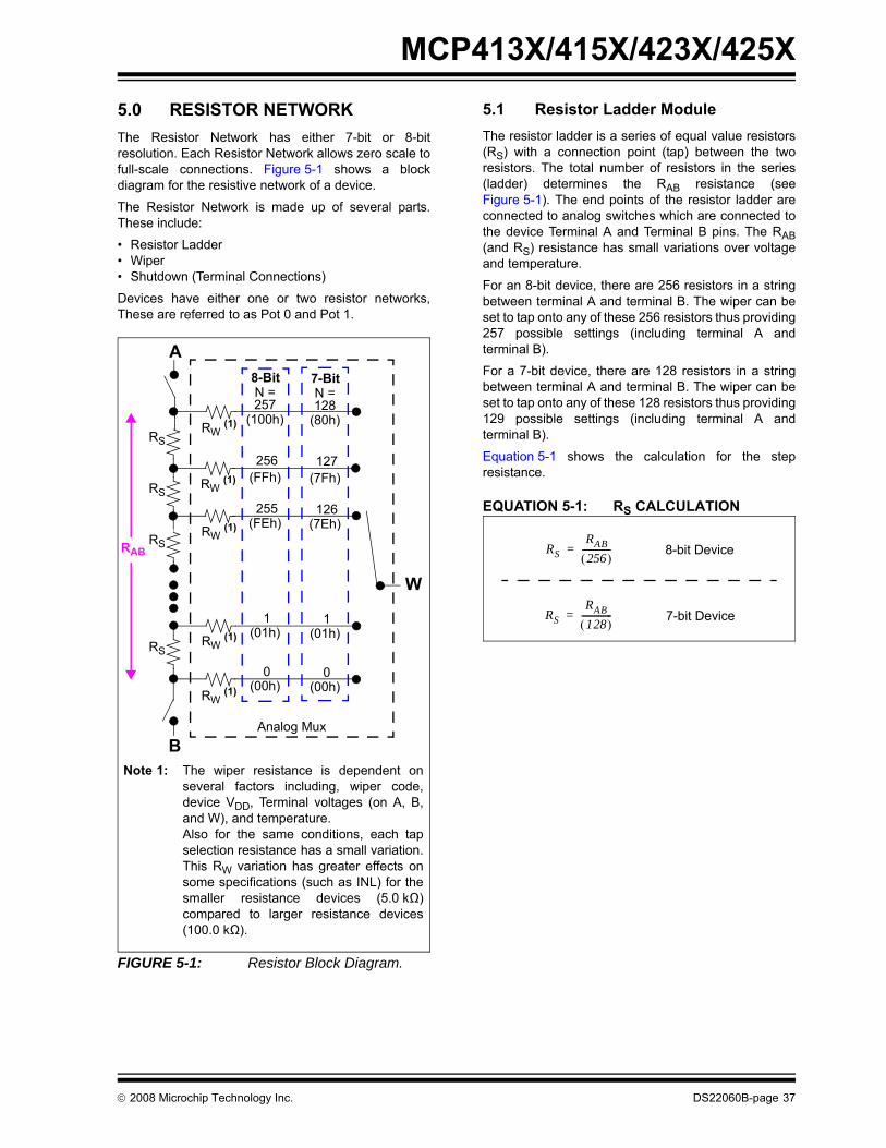
5.0 RESISTOR NETWORKThe Resistor Network has either 7-bit or 8-bitresolution. Each Resistor Network allows zero scale tofull-scale connections. Figure 5-1 shows a blockdiagram for the resistive network of a device.
The Resistor Network is made up of several parts.These include:
• Resistor Ladder• Wiper• Shutdown (Terminal Connections)
Devices have either one or two resistor networks,These are referred to as Pot 0 and Pot 1.
FIGURE 5-1: Resistor Block Diagram.
5.1 Resistor Ladder ModuleThe resistor ladder is a series of equal value resistors(RS) with a connection point (tap) between the tworesistors. The total number of resistors in the series(ladder) determines the RAB resistance (seeFigure 5-1). The end points of the resistor ladder areconnected to analog switches which are connected tothe device Terminal A and Terminal B pins. The RAB(and RS) resistance has small variations over voltageand temperature.
For an 8-bit device, there are 256 resistors in a stringbetween terminal A and terminal B. The wiper can beset to tap onto any of these 256 resistors thus providing257 possible settings (including terminal A andterminal B).
For a 7-bit device, there are 128 resistors in a stringbetween terminal A and terminal B. The wiper can beset to tap onto any of these 128 resistors thus providing129 possible settings (including terminal A andterminal B).
Equation 5-1 shows the calculation for the stepresistance.
EQUATION 5-1: RS CALCULATION
RS
A
RS
RS
RS
B
257
256
255
1
0
RW (1)
W
(01h)
Analog Mux
RW (1) (00h)
RW (1) (FEh)
RW (1) (FFh)
RW (1) (100h)
Note 1: The wiper resistance is dependent onseveral factors including, wiper code,device VDD, Terminal voltages (on A, B,and W), and temperature. Also for the same conditions, each tapselection resistance has a small variation.This RW variation has greater effects onsome specifications (such as INL) for thesmaller resistance devices (5.0 kΩ)compared to larger resistance devices(100.0 kΩ).
RAB
8-BitN =
128
127
126
1
0
(01h)
(00h)
(7Eh)
(7Fh)
(80h)
7-BitN =
RSRAB256( )
-------------=
RSRAB128( )
--------------=
8-bit Device
7-bit Device
© 2008 Microchip Technology Inc. DS22060B-page 37

MCP413X/415X/423X/425X
5.2 WiperEach tap point (between the RS resistors) is aconnection point for an analog switch. The oppositeside of the analog switch is connected to a commonsignal which is connected to the Terminal W (Wiper)pin.A value in the volatile wiper register selects whichanalog switch to close, connecting the W terminal tothe selected node of the resistor ladder.
The wiper can connect directly to Terminal B or toTerminal A. A zero-scale connections, connects theTerminal W (wiper) to Terminal B (wiper setting of000h). A full-scale connections, connects the TerminalW (wiper) to Terminal A (wiper setting of 100h or 80h).In these configurations the only resistance between theTerminal W and the other Terminal (A or B) is that of theanalog switches.
A wiper setting value greater than full-scale (wipersetting of 100h for 8-bit device or 80h for 7-bit devices)will also be a Full-Scale setting (Terminal W (wiper)connected to Terminal A). Table 5-1 illustrates the fullwiper setting map.
Equation 5-2 illustrates the calculation used to deter-mine the resistance between the wiper and terminal B.
EQUATION 5-2: RWB CALCULATION
TABLE 5-1: VOLATILE WIPER VALUE VS. WIPER POSITION MAP
A POR/BOR event will load the Volatile Wiper registervalue with the default value. Table 5-2 shows thedefault values offered. Custom POR/BOR options areavailable. Contact the local Microchip Sales Office.
TABLE 5-2: DEFAULT FACTORY SETTINGS SELECTION
Wiper SettingProperties
7-bit Pot 8-bit Pot3FFh081h
3FFh101h
Reserved (Full-Scale (W = A)),Increment and Decrement commands ignored
080h 100h Full-Scale (W = A), Increment commands ignored
07Fh041h
0FFh081
W = N
040h 080h W = N (Mid-Scale)03Fh001h
07Fh001
W = N
000h 000h Zero Scale (W = B)Decrement command ignored
RWBRABN256( )
-------------- RW+=
N = 0 to 256 (decimal)
RWBRABN128( )
-------------- RW+=
N = 0 to 128 (decimal)
8-bit Device
7-bit Device
Res
ista
nce
Cod
e
Typi
cal
RA
B V
alue
Def
ault
POR
W
iper
Set
ting Wiper Code
8-bit 7-bit
-502 5.0 kΩ Mid-scale 80h 40h-103 10.0 kΩ Mid-scale 80h 40h-503 50.0 kΩ Mid-scale 80h 40h-104 100.0 kΩ Mid-scale 80h 40h
DS22060B-page 38 © 2008 Microchip Technology Inc.
MCP413X/415X/423X/425X
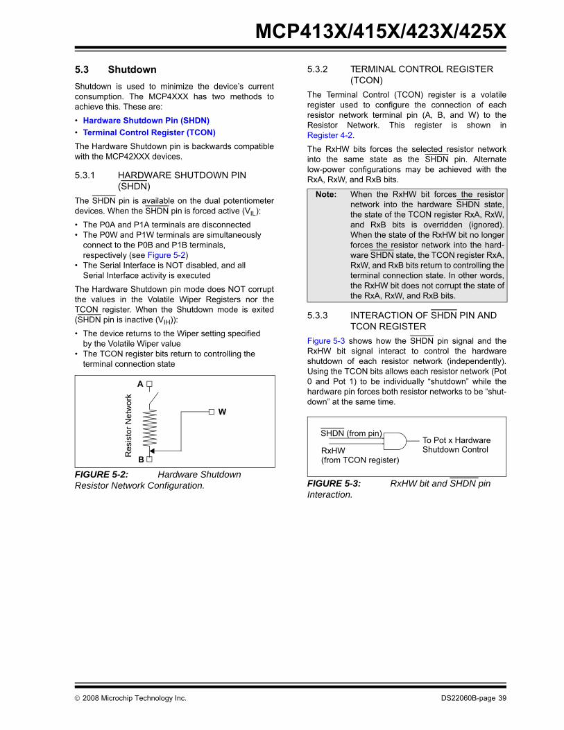
5.3 Shutdown Shutdown is used to minimize the device’s currentconsumption. The MCP4XXX has two methods toachieve this. These are:• Hardware Shutdown Pin (SHDN) • Terminal Control Register (TCON) The Hardware Shutdown pin is backwards compatiblewith the MCP42XXX devices.
5.3.1 HARDWARE SHUTDOWN PIN (SHDN)
The SHDN pin is available on the dual potentiometerdevices. When the SHDN pin is forced active (VIL):
• The P0A and P1A terminals are disconnected• The P0W and P1W terminals are simultaneously
connect to the P0B and P1B terminals, respectively (see Figure 5-2)
• The Serial Interface is NOT disabled, and all Serial Interface activity is executed
The Hardware Shutdown pin mode does NOT corruptthe values in the Volatile Wiper Registers nor theTCON register. When the Shutdown mode is exited(SHDN pin is inactive (VIH)):
• The device returns to the Wiper setting specified by the Volatile Wiper value
• The TCON register bits return to controlling the terminal connection state
FIGURE 5-2: Hardware Shutdown Resistor Network Configuration.
5.3.2 TERMINAL CONTROL REGISTER (TCON)
The Terminal Control (TCON) register is a volatileregister used to configure the connection of eachresistor network terminal pin (A, B, and W) to theResistor Network. This register is shown inRegister 4-2.
The RxHW bits forces the selected resistor networkinto the same state as the SHDN pin. Alternatelow-power configurations may be achieved with theRxA, RxW, and RxB bits.
5.3.3 INTERACTION OF SHDN PIN AND TCON REGISTER
Figure 5-3 shows how the SHDN pin signal and theRxHW bit signal interact to control the hardwareshutdown of each resistor network (independently).Using the TCON bits allows each resistor network (Pot0 and Pot 1) to be individually “shutdown” while thehardware pin forces both resistor networks to be “shut-down” at the same time.
FIGURE 5-3: RxHW bit and SHDN pin Interaction.
A
B
W
Res
isto
r Net
wor
k
Note: When the RxHW bit forces the resistornetwork into the hardware SHDN state,the state of the TCON register RxA, RxW,and RxB bits is overridden (ignored).When the state of the RxHW bit no longerforces the resistor network into the hard-ware SHDN state, the TCON register RxA,RxW, and RxB bits return to controlling theterminal connection state. In other words,the RxHW bit does not corrupt the state ofthe RxA, RxW, and RxB bits.
SHDN (from pin)
RxHW (from TCON register)
To Pot x Hardware Shutdown Control
© 2008 Microchip Technology Inc. DS22060B-page 39

MCP413X/415X/423X/425X
NOTES:DS22060B-page 40 © 2008 Microchip Technology Inc.

MCP413X/415X/423X/425X
6.0 SERIAL INTERFACE (SPI) The MCP4XXX devices support the SPI serial protocol.This SPI operates in the slave mode (does notgenerate the serial clock).
The SPI interface uses up to four pins. These are:
• CS - Chip Select • SCK - Serial Clock • SDI - Serial Data In • SDO - Serial Data Out
Typical SPI Interfaces are shown in Figure 6-1. In theSPI interface, The Master’s Output pin is connected tothe Slave’s Input pin and the Master’s Input pin isconnected to the Slave’s Output pin.
The MCP4XXX SPI’s module supports two (of the four)standard SPI modes. These are Mode 0,0 and 1,1.The SPI mode is determined by the state of the SCKpin (VIH or VIL) on the when the CS pin transitions frominactive (VIH) to active (VIL or VIHH).
All SPI interface signals are high-voltage tolerant.
FIGURE 6-1: Typical SPI Interface Block Diagram.
SDI/SDOSDI
SDO
SDO
SDI R1(2)
MCP41X1
SCK SCK
SDISDO
MCP4XXX
SDOSDI
SCKSCK
( Master Out - Slave In (MOSI) )
( Master In - Slave Out (MISO) )
HostController
HostController
Typical SPI Interface Connections
Typical MCP41X1 SPI Interface Connections (Host Controller Hardware SPI)
SDI/SDOSDI
SDO
I/O
MCP41X1
I/O SCK
HostController
Alternate MCP41X1 SPI Interface Connections (Host Controller Firmware SPI)
(SDO/SDI)
(SCK)
CSI/O (1)
CSI/O (1)
CSI/O (1)
Note 1: If High voltage commands are desired, some type of external circuitry needs to beimplemented.
2: R1 must be sized to ensure VIL and VIH of the devices are met.
© 2008 Microchip Technology Inc. DS22060B-page 41

MCP413X/415X/423X/425X
6.1 SDI, SDO, SCK, and CS OperationThe operation of the four SPI interface pins arediscussed in this section. These pins are:• SDI (Serial Data In)• SDO (Serial Data Out)• SCK (Serial Clock)• CS (Chip Select)
The serial interface works on either 8-bit or 16-bitboundaries depending on the selected command. TheChip Select (CS) pin frames the SPI commands.
6.1.1 SERIAL DATA IN (SDI)The Serial Data In (SDI) signal is the data signal intothe device. The value on this pin is latched on the risingedge of the SCK signal.
6.1.2 SERIAL DATA OUT (SDO)The Serial Data Out (SDO) signal is the data signal outof the device. The value on this pin is driven on thefalling edge of the SCK signal.
Once the CS pin is forced to the active level (VIL orVIHH), the SDO pin will be driven. The state of the SDOpin is determined by the serial bit’s position in thecommand, the command selected, and if there is acommand error state (CMDERR).
6.1.3 SDI/SDO
For device packages that do not have enough pins forboth an SDI and SDO pin, the SDI and SDOfunctionality is multiplexed onto a single I/O pin calledSDI/SDO.
The SDO will only be driven for the command error bit(CMDERR) and during the data bits of a read command(after the memory address and command has beenreceived).
6.1.3.1 SDI/SDO Operation Figure 6-2 shows a block diagram of the SDI/SDO pin.The SDI signal has an internal “smart” pull-up. Thevalue of this pull-up determines the frequency that datacan be read from the device. An external pull-up can beadded to the SDI/SDO pin to improve the rise time andtherefore improve the frequency that data can be read.
Data written on the SDI/SDO pin can be at themaximum SPI frequency.
On the falling edge of the SCK pin during the C0 bit(see Figure 7-1), the SDI/SDO pin will start outputtingthe SDO value. The SDO signal overrides the control ofthe smart pull-up, such that whenever the SDI/SDO pinis outputting data, the smart pull-up is enabled.
The SDI/SDO pin will change from an input (SDI) to anoutput (SDO) after the state machine has received theAddress and Command bits of the Command Byte. Ifthe command is a Read command, then the SDI/SDOpin will remain an output for the remainder of thecommand. For any other command, the SDI/SDO pinreturns to an input.
FIGURE 6-2: Serial I/O Mux Block Diagram.
Note: MCP41X1 Devices Only .
Note: To support the High voltage requirement ofthe SDI function, the SDO function is anopen drain output.
Note: Care must be take to ensure that a Driveconflict does not exist between the HostControllers SDO pin (or software SDI/SDOpin) and the MCP41x1 SDI/SDO pin (seeFigure 6-1).
SDI/SDO SDI
SDOControl
“smart” pull-up
OpenDrain
Logic
DS22060B-page 42 © 2008 Microchip Technology Inc.
MCP413X/415X/423X/425X
6.1.4 SERIAL CLOCK (SCK)(SPI FREQUENCY OF OPERATION) The SPI interface is specified to operate up to 10 MHz.The actual clock rate depends on the configuration ofthe system and the serial command used. Table 6-1shows the SCK frequency for different configurations.
TABLE 6-1: SCK FREQUENCY
6.1.5 THE CS SIGNAL The Chip Select (CS) signal is used to select the deviceand frame a command sequence. To start a command,or sequence of commands, the CS signal musttransition from the inactive state (VIH) to an active state(VIL or VIHH).
After the CS signal has gone active, the SDO pin isdriven and the clock bit counter is reset.
If an error condition occurs for an SPI command, thenthe Command byte’s Command Error (CMDERR) bit(on the SDO pin) will be driven low (VIL). To exit theerror condition, the user must take the CS pin to the VIHlevel.
When the CS pin returns to the inactive state (VIH) theSPI module resets (including the address pointer).While the CS pin is in the inactive state (VIH), the serialinterface is ignored. This allows the Host Controller tointerface to other SPI devices using the same SDI,SDO, and SCK signals.
The CS pin has an internal pull-up resistor. The resistoris disabled when the voltage on the CS pin is at the VILlevel. This means that when the CS pin is not driven,the internal pull-up resistor will pull this signal to the VIHlevel. When the CS pin is driven low (VIL), theresistance becomes very large to reduce the devicecurrent consumption.
The high voltage capability of the CS pin allowsMCP413X/415X/423X/425X devices to be used insystems previously designed for the MCP414X/416X/424X/426X devices.
Memory Type Access
Command
ReadWrite,
Increment, Decrement
Volatile Memory
SDI, SDO 10 MHz 10 MHzSDI/SDO (1) 250 kHz (2) 10 MHz
Note 1: MCP41X1 devices only.
2: This is the maximum clock frequencywithout an external pull-up resistor.
Note: There is a required delay after the CS pingoes active to the 1st edge of the SCK pin.
© 2008 Microchip Technology Inc. DS22060B-page 43
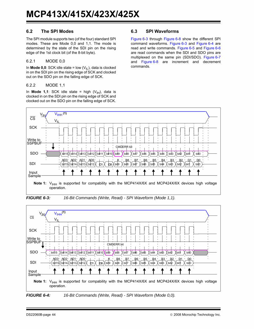
MCP413X/415X/423X/425X
6.2 The SPI ModesThe SPI module supports two (of the four) standard SPImodes. These are Mode 0,0 and 1,1. The mode isdetermined by the state of the SDI pin on the risingedge of the 1st clock bit (of the 8-bit byte).6.2.1 MODE 0,0 In Mode 0,0: SCK idle state = low (VIL), data is clockedin on the SDI pin on the rising edge of SCK and clockedout on the SDO pin on the falling edge of SCK.
6.2.2 MODE 1,1 In Mode 1,1: SCK idle state = high (VIH), data isclocked in on the SDI pin on the rising edge of SCK andclocked out on the SDO pin on the falling edge of SCK.
6.3 SPI WaveformsFigure 6-3 through Figure 6-8 show the different SPIcommand waveforms. Figure 6-3 and Figure 6-4 areread and write commands. Figure 6-5 and Figure 6-6are read commands when the SDI and SDO pins aremultiplexed on the same pin (SDI/SDO). Figure 6-7and Figure 6-8 are increment and decrementcommands.
FIGURE 6-3: 16-Bit Commands (Write, Read) - SPI Waveform (Mode 1,1).
FIGURE 6-4: 16-Bit Commands (Write, Read) - SPI Waveform (Mode 0,0).
CS
SCK
Write toSSPBUF
SDI
InputSample
SDO bit15 bit14 bit13 bit12 bit11 bit10 bit9 bit8 bit7 bit6 bit5 bit4 bit3 bit2 bit1 bit0
bit15 bit14 bit13 bit12 bit9 bit8 bit7 bit6 bit5 bit4 bit3 bit2 bit1 bit0AD3 AD2 AD1 AD0
C1 C0X D8 D7 D6 D5 D4 D3 D2 D1 D0
VIH
VIL
CMDERR bit
VIHH (1)
Note 1: VIHH is supported for compability with the MCP414X/6X and MCP424X/6X devices high voltageoperation.
CS
SCK
Write toSSPBUF
SDI
InputSample
SDO bit15 bit14 bit13 bit12 bit11 bit10 bit9 bit8 bit7 bit6 bit5 bit4 bit3 bit2 bit1 bit0
bit15 bit14 bit13 bit12 bit9 bit8 bit7 bit6 bit5 bit4 bit3 bit2 bit1 bit0AD3 AD2 AD1 AD0
C1 C0X D8 D7 D6 D5 D4 D3 D2 D1 D0
VIH
VIL
CMDERR bit
VIHH(1)
Note 1: VIHH is supported for compability with the MCP414X/6X and MCP424X/6X devices high voltageoperation.
DS22060B-page 44 © 2008 Microchip Technology Inc.

MCP413X/415X/423X/425X
FIGURE 6-5: 16-Bit Read Command for Devices with SDI/SDO multiplexed - SPI Waveform (Mode 1,1).
FIGURE 6-6: 16-Bit Read Command for Devices with SDI/SDO multiplexed - SPI Waveform (Mode 0,0).
CS
SCK
Write toSSPBUF
SDI
InputSample
SDO bit9 bit8 bit7 bit6 bit5 bit4 bit3 bit2 bit1 bit0
bit15 bit14 bit13 bit12AD3 AD2 AD1 AD0 C1 C0
D9 D8 D7 D6 D5 D4 D3 D2 D1 D0
VIH VIL
CMDERR bit
(1) (1) (1) (1) (1) (1) (1) (1) (1) (1)1 1
VIHH (1)
Note 1: The SDI pin will read the state of the SDI pin which will be the SDO signal, unless overdriven.
2: VIHH is supported for compability with the MCP414X/6X and MCP424X/6X devices high voltageoperation.
CS
SCK
Write toSSPBUF
SDI
InputSample
SDO bit9 bit8 bit7 bit6 bit5 bit4 bit3 bit2 bit1 bit0
bit15 bit14 bit13 bit12AD3 AD2 AD1 AD0 C1 C0
D8 D7 D6 D5 D4 D3 D2 D1 D0X
VIH VIL
CMDERR bit
(1) (1) (1) (1) (1) (1) (1) (1) (1) (1)1 1
VIHH (1)
Note 1: The SDI pin will read the state of the SDI pin which will be the SDO signal, unless overdriven.
2: VIHH is supported for compability with the MCP414X/6X and MCP424X/6X devices high voltageoperation.
© 2008 Microchip Technology Inc. DS22060B-page 45
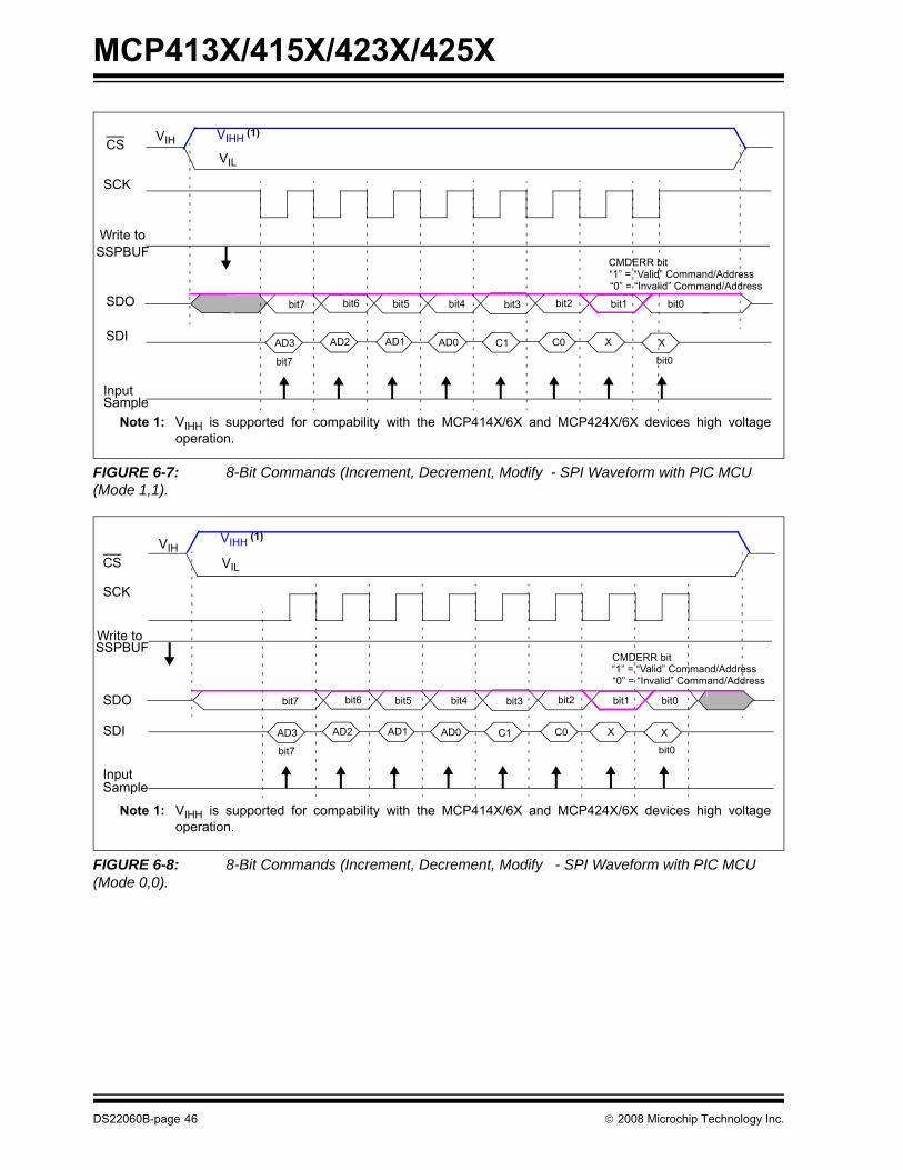
MCP413X/415X/423X/425X
FIGURE 6-7: 8-Bit Commands (Increment, Decrement, Modify - SPI Waveform with PIC MCU (Mode 1,1).
FIGURE 6-8: 8-Bit Commands (Increment, Decrement, Modify - SPI Waveform with PIC MCU (Mode 0,0).
bit7 bit0
bit7 bit6 bit5 bit4 bit3 bit2 bit1 bit0
CS
SCK
Write toSSPBUF
SDI
InputSample
SDO
VIH
VIL
AD3 AD2 AD1 AD0 C0 C1 X X
“1” = “Valid” Command/Address “0” = “Invalid” Command/Address
CMDERR bit
VIHH (1)
Note 1: VIHH is supported for compability with the MCP414X/6X and MCP424X/6X devices high voltageoperation.
SCK
InputSample
SDIbit7 bit0
SDO bit7 bit6 bit5 bit4 bit3 bit2 bit1 bit0
Write toSSPBUF
CSVIH
VIL
AD3 AD2 AD1 AD0 C0 C1 X X
“1” = “Valid” Command/Address “0” = “Invalid” Command/Address
CMDERR bit
VIHH (1)
Note 1: VIHH is supported for compability with the MCP414X/6X and MCP424X/6X devices high voltageoperation.
DS22060B-page 46 © 2008 Microchip Technology Inc.

MCP413X/415X/423X/425X
7.0 DEVICE COMMANDSThe MCP4XXX’s SPI command format supports 16memory address locations and four commands. Eachcommand has two modes. These are:
• Normal Serial Commands• High-Voltage Serial Commands
Normal serial commands are those where the CS pin isdriven to VIL. High Voltage Serial Commands, CS pin isdriven to VIHH, for compatibility with systems that alsosupport the MCP414X/416X/424X/426X devices. HighVoltage Serial Commands operate identically to theircorresponding Normal Serial Command. In eachmode, there are four possible commands. Thesecommands are shown in Table 7-1.
The 8-bit commands (Increment Wiper and Decre-ment Wiper commands) contain a Command Byte,see Figure 7-1, while 16-bit commands (Read Dataand Write Data commands) contain a Command Byteand a Data Byte. The Command Byte contains two databits, see Figure 7-1.
Table 7-2 shows the supported commands for eachmemory location and the corresponding values on theSDI and SDO pins.
Table 7-3 shows an overview of all the SPI commandsand their interaction with other device features.
7.1 Command ByteThe Command Byte has three fields, the Address, theCommand, and 2 Data bits, see Figure 7-1. Currentlyonly one of the data bits is defined (D8). This is for theWrite command.
The device memory is accessed when the mastersends a proper Command Byte to select the desiredoperation. The memory location getting accessed iscontained in the Command Byte’s AD3:AD0 bits. Theaction desired is contained in the Command Byte’sC1:C0 bits, see Table 7-1. C1:C0 determines if thedesired memory location will be read, written,Incremented (wiper setting +1) or Decremented (wipersetting -1). The Increment and Decrement commandsare only valid on the volatile wiper registers.
As the Command Byte is being loaded into the device(on the SDI pin), the device’s SDO pin is driving. TheSDO pin will output high bits for the first six bits of thatcommand. On the 7th bit, the SDO pin will output theCMDERR bit state (see Section 7.3 “Error Condi-tion”). The 8th bit state depends on the the commandselected.
TABLE 7-1: COMMAND BIT OVERVIEW
FIGURE 7-1: General SPI Command Formats.
C1:C0 Bit States Command # of Bits
11 Read Data 16-Bits
00 Write Data 16-Bits
01 Increment 8-Bits
10 Decrement 8-Bits
AD3
AD2
AD1
AD0
C1
C0
D9
D8
Memory
Command Byte
Data Address Bits
CommandBits
AD3
AD2
AD1
AD0
C1
C0
D9
D8
D7
D6
D5
D4
D3
D2
D1
D0
Memory
16-bit Command
Data Address Bits
CommandBits
0 0 = Write Data0 1 = INCR1 0 = DECR1 1 = Read Data
C C1 0
CommandBits
8-bit Command
Command Byte Data Byte
© 2008 Microchip Technology Inc. DS22060B-page 47

MCP413X/415X/423X/425X
TABLE 7-2: MEMORY MAP AND THE SUPPORTED COMMANDSAddressCommand Data
(10-bits) (1) SPI String (Binary)
Value Function MOSI (SDI pin) MISO (SDO pin) (2)
00h Volatile Wiper 0 Write Data nn nnnn nnnn 0000 00nn nnnn nnnn 1111 1111 1111 1111Read Data nn nnnn nnnn 0000 11nn nnnn nnnn 1111 111n nnnn nnnnIncrement Wiper — 0000 0100 1111 1111Decrement Wiper — 0000 1000 1111 1111
01h Volatile Wiper 1 Write Data nn nnnn nnnn 0001 00nn nnnn nnnn 1111 1111 1111 1111Read Data nn nnnn nnnn 0001 11nn nnnn nnnn 1111 111n nnnn nnnnIncrement Wiper — 0001 0100 1111 1111Decrement Wiper — 0001 1000 1111 1111
02h Reserved — — — —03h Reserved — — — —04h Volatile
TCON RegisterWrite Data nn nnnn nnnn 0100 00nn nnnn nnnn 1111 1111 1111 1111Read Data nn nnnn nnnn 0100 11nn nnnn nnnn 1111 111n nnnn nnnn
05h Status Register Read Data nn nnnn nnnn 0101 11nn nnnn nnnn 1111 111n nnnn nnnn06h-0Fh Reserved — — — —
Note 1: The Data Memory is only 9-bits wide, so the MSb is ignored by the device. 2: All these Address/Command combinations are valid, so the CMDERR bit is set. Any other Address/Command
combination is a command error state and the CMDERR bit will be clear.
DS22060B-page 48 © 2008 Microchip Technology Inc.

MCP413X/415X/423X/425X
7.2 Data ByteOnly the Read Command and the Write Command usethe Data Byte, see Figure 7-1. These commandsconcatenate the 8-bits of the Data Byte with the onedata bit (D8) contained in the Command Byte to form9-bits of data (D8:D0). The Command Byte formatsupports up to 9-bits of data so that the 8-bit resistornetwork can be set to Full-Scale (100h or greater). Thisallows wiper connections to Terminal A and toTerminal B.The D9 bit is currently unused, and corresponds to theposition on the SDO data of the CMDERR bit.
7.3 Error ConditionThe CMDERR bit indicates if the four address bitsreceived (AD3:AD0) and the two command bitsreceived (C1:C0) are a valid combination (seeTable 4-1). The CMDERR bit is high if the combinationis valid and low if the combination is invalid.
SPI commands that do not have a multiple of 8 clocksare ignored.
Once an error condition has occurred, any followingcommands are ignored. All following SDO bits will below until the CMDERR condition is cleared by forcingthe CS pin to the inactive state (VIH).
7.3.1 ABORTING A TRANSMISSIONAll SPI transmissions must have the correct number ofSCK pulses to be executed. The command is notexecuted until the complete number of clocks havebeen received. If the CS pin is forced to the inactivestate (VIH) the serial interface is reset. Partial com-mands are not executed.
SPI is more susceptible to noise than other busprotocols. The most likely case is that this noisecorrupts the value of the data being clocked into theMCP4XXX or the SCK pin is injected with extra clockpulses. This may cause data to be corrupted in thedevice, or a command error to occur, since the addressand command bits were not a valid combination. Theextra SCK pulse will also cause the SPI data (SDI) andclock (SCK) to be out of sync. Forcing the CS pin to theinactive state (VIH) resets the serial interface. The SPIinterface will ignore activity on the SDI and SCK pinsuntil the CS pin transition to the active state is detected(VIH to VIL or VIH to VIHH).
Note 1: When data is not being received by theMCP4XXX, It is recommended that theCS pin be forced to the inactive level (VIL)
2: It is also recommended that longcontinuous command strings should bebroken down into single commands orshorter continuous command strings.This reduces the probability of noise onthe SCK pin corrupting the desired SPIcommands.
© 2008 Microchip Technology Inc. DS22060B-page 49

MCP413X/415X/423X/425X
7.4 Continuous Commands The device supports the ability to execute commandscontinuously. While the CS pin is in the active state(VIL or VIHH). Any sequence of valid commands may bereceived.The following example is a valid sequence of events:
1. CS pin driven active (VIL or VIHH).2. Read Command.3. Increment Command (Wiper 0).4. Increment Command (Wiper 0).5. Decrement Command (Wiper 1).6. Write Command.7. Write Command.8. CS pin driven inactive (VIH).
TABLE 7-3: COMMANDS
Note 1: It is recommended that while the CS pin isactive, only one type of command shouldbe issued. When changing commands, itis recommended to take the CS pininactive then force it back to the activestate.
2: It is also recommended that longcommand strings should be broken downinto shorter command strings. Thisreduces the probability of noise on theSCK pin corrupting the desired SPIcommand string.
Command Name # of BitsHigh Voltage (VIHH) on CS
pin?
Write Data 16-Bits —Read Data 16-Bits —Increment Wiper 8-Bits —Decrement Wiper 8-Bits —High Voltage Write Data 16-Bits YesHigh Voltage Read Data 16-Bits YesHigh Voltage Increment Wiper 8-Bits YesHigh Voltage Decrement Wiper 8-Bits Yes
DS22060B-page 50 © 2008 Microchip Technology Inc.
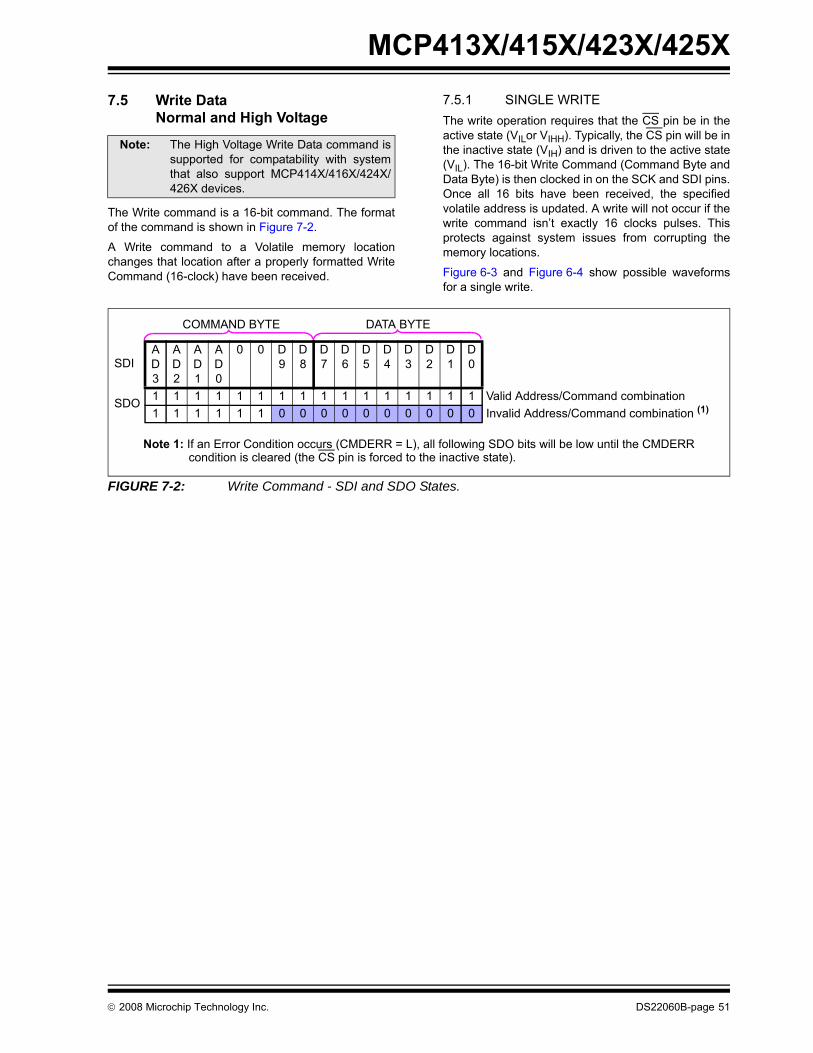
MCP413X/415X/423X/425X
7.5 Write DataNormal and High Voltage
The Write command is a 16-bit command. The formatof the command is shown in Figure 7-2.
A Write command to a Volatile memory locationchanges that location after a properly formatted WriteCommand (16-clock) have been received.
7.5.1 SINGLE WRITEThe write operation requires that the CS pin be in theactive state (VILor VIHH). Typically, the CS pin will be inthe inactive state (VIH) and is driven to the active state(VIL). The 16-bit Write Command (Command Byte andData Byte) is then clocked in on the SCK and SDI pins.Once all 16 bits have been received, the specifiedvolatile address is updated. A write will not occur if thewrite command isn’t exactly 16 clocks pulses. Thisprotects against system issues from corrupting thememory locations.
Figure 6-3 and Figure 6-4 show possible waveformsfor a single write.
FIGURE 7-2: Write Command - SDI and SDO States.
Note: The High Voltage Write Data command issupported for compatability with systemthat also support MCP414X/416X/424X/426X devices.
AD3
AD2
AD1
AD0
0 0 D9
D8
D7
D6
D5
D4
D3
D2
D1
D0
1 1 1 1 1 1 1 1 1 1 1 1 1 1 1 1 Valid Address/Command combination1 1 1 1 1 1 0 0 0 0 0 0 0 0 0 0 Invalid Address/Command combination (1)
COMMAND BYTE DATA BYTE
SDI
SDO
Note 1: If an Error Condition occurs (CMDERR = L), all following SDO bits will be low until the CMDERRcondition is cleared (the CS pin is forced to the inactive state).
© 2008 Microchip Technology Inc. DS22060B-page 51

MCP413X/415X/423X/425X
7.5.2 CONTINUOUS WRITES Continuous writes are possible only when writing to thevolatile memory registers (address 00h, 01h, and 04h).Figure 7-3 shows the sequence for three continuouswrites. The writes do not need to be to the same volatilememory address.
FIGURE 7-3: Continuous Write Sequence.
AD3
AD2
AD1
AD0
0 0 D9
D8
D7
D6
D5
D4
D3
D2
D1
D0
1 1 1 1 1 1 1* 1 1 1 1 1 1 1 1 1
AD3
AD2
AD1
AD0
0 0 D9
D8
D7
D6
D5
D4
D3
D2
D1
D0
1 1 1 1 1 1 1* 1 1 1 1 1 1 1 1 1
AD3
AD2
AD1
AD0
0 0 D9
D8
D7
D6
D5
D4
D3
D2
D1
D0
1 1 1 1 1 1 1* 1 1 1 1 1 1 1 1 1
COMMAND BYTE DATA BYTE
SDI
SDO
Note 1: If a Command Error (CMDERR) occurs at this bit location (*), then all following SDO bits will bedriven low until the CS pin is driven inactive (VIH).
DS22060B-page 52 © 2008 Microchip Technology Inc.
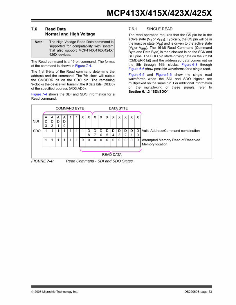
MCP413X/415X/423X/425X
7.6 Read DataNormal and High Voltage
The Read command is a 16-bit command. The formatof the command is shown in Figure 7-4.
The first 6-bits of the Read command determine theaddress and the command. The 7th clock will outputthe CMDERR bit on the SDO pin. The remaining9-clocks the device will transmit the 9 data bits (D8:D0)of the specified address (AD3:AD0).
Figure 7-4 shows the SDI and SDO information for aRead command.
7.6.1 SINGLE READThe read operation requires that the CS pin be in theactive state (VILor VIHH). Typically, the CS pin will be inthe inactive state (VIH) and is driven to the active state(VILor VIHH). The 16-bit Read Command (CommandByte and Data Byte) is then clocked in on the SCK andSDI pins. The SDO pin starts driving data on the 7th bit(CMDERR bit) and the addressed data comes out onthe 8th through 16th clocks. Figure 6-3 throughFigure 6-6 show possible waveforms for a single read.
Figure 6-5 and Figure 6-6 show the single readwaveforms when the SDI and SDO signals aremultiplexed on the same pin. For additional informationon the multiplexing of these signals, refer toSection 6.1.3 “SDI/SDO”.
FIGURE 7-4: Read Command - SDI and SDO States.
Note: The High Voltage Read Data command issupported for compatability with systemthat also support MCP414X/416X/424X/426X devices.
AD3
AD2
AD1
AD0
1 1 X X X X X X X X X X
1 1 1 1 1 1 1 D8
D7
D6
D5
D4
D3
D2
D1
D0
Valid Address/Command combination
1 1 1 1 1 1 0 0 0 0 0 0 0 0 0 0 Attempted Memory Read of ReservedMemory location.
COMMAND BYTE DATA BYTE
SDI
SDO
READ DATA
© 2008 Microchip Technology Inc. DS22060B-page 53

MCP413X/415X/423X/425X
7.6.2 CONTINUOUS READS Continuous reads allows the devices memory to beread quickly. Continuous reads are possible to allmemory locations.Figure 7-5 shows the sequence for three continuousreads. The reads do not need to be to the samememory address.
FIGURE 7-5: Continuous Read Sequence.
AD3
AD2
AD1
AD0
1 1 X X X X X X X X X X
1 1 1 1 1 1 1* D8
D7
D6
D5
D4
D3
D2
D1
D0
AD3
AD2
AD1
AD0
1 1 X X X X X X X X X X
1 1 1 1 1 1 1* D8
D7
D6
D5
D4
D3
D2
D1
D0
AD3
AD2
AD1
AD0
1 1 X X X X X X X X X X
1 1 1 1 1 1 1* D8
D7
D6
D5
D4
D3
D2
D1
D0
COMMAND BYTE DATA BYTE
SDI
SDO
Note 1: If a Command Error (CMDERR) occurs at this bit location (*), then all following SDO bits will bedriven low until the CS pin is driven inactive (VIH).
DS22060B-page 54 © 2008 Microchip Technology Inc.
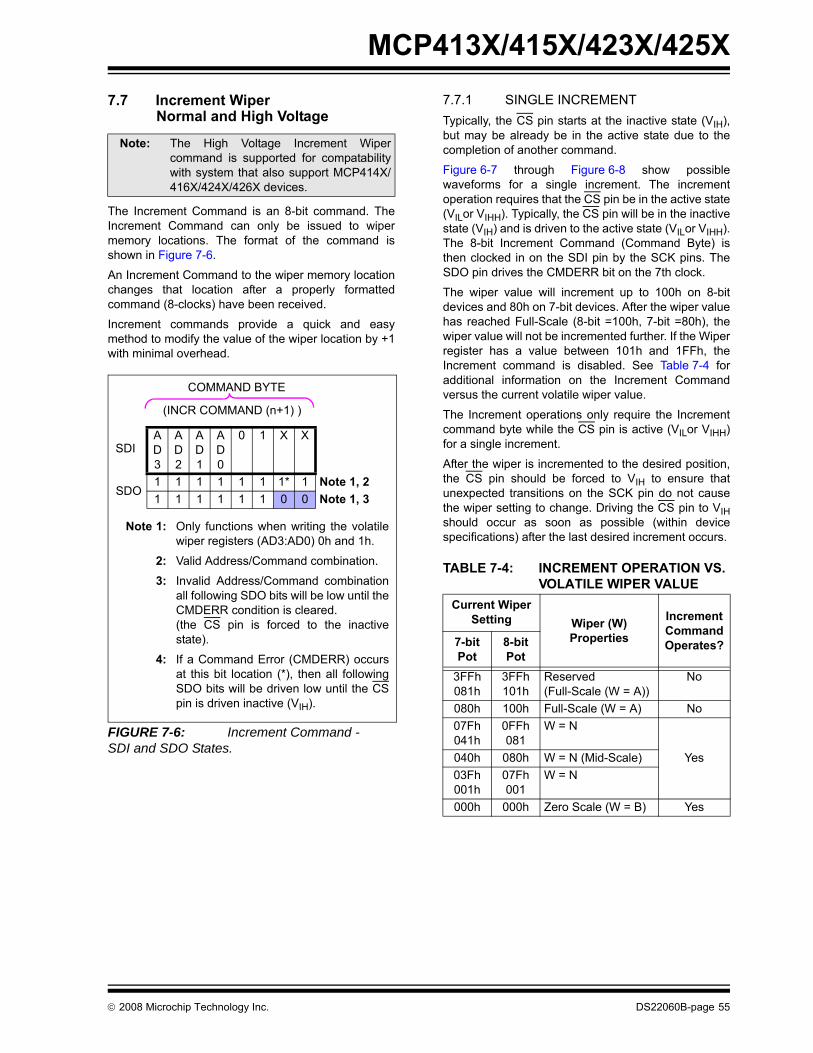
MCP413X/415X/423X/425X
7.7 Increment WiperNormal and High Voltage
The Increment Command is an 8-bit command. TheIncrement Command can only be issued to wipermemory locations. The format of the command isshown in Figure 7-6.
An Increment Command to the wiper memory locationchanges that location after a properly formattedcommand (8-clocks) have been received.
Increment commands provide a quick and easymethod to modify the value of the wiper location by +1with minimal overhead.
FIGURE 7-6: Increment Command - SDI and SDO States.
7.7.1 SINGLE INCREMENT Typically, the CS pin starts at the inactive state (VIH),but may be already be in the active state due to thecompletion of another command.
Figure 6-7 through Figure 6-8 show possiblewaveforms for a single increment. The incrementoperation requires that the CS pin be in the active state(VILor VIHH). Typically, the CS pin will be in the inactivestate (VIH) and is driven to the active state (VILor VIHH).The 8-bit Increment Command (Command Byte) isthen clocked in on the SDI pin by the SCK pins. TheSDO pin drives the CMDERR bit on the 7th clock.
The wiper value will increment up to 100h on 8-bitdevices and 80h on 7-bit devices. After the wiper valuehas reached Full-Scale (8-bit =100h, 7-bit =80h), thewiper value will not be incremented further. If the Wiperregister has a value between 101h and 1FFh, theIncrement command is disabled. See Table 7-4 foradditional information on the Increment Commandversus the current volatile wiper value.
The Increment operations only require the Incrementcommand byte while the CS pin is active (VILor VIHH)for a single increment.
After the wiper is incremented to the desired position,the CS pin should be forced to VIH to ensure thatunexpected transitions on the SCK pin do not causethe wiper setting to change. Driving the CS pin to VIHshould occur as soon as possible (within devicespecifications) after the last desired increment occurs.
TABLE 7-4: INCREMENT OPERATION VS. VOLATILE WIPER VALUE
Note: The High Voltage Increment Wipercommand is supported for compatabilitywith system that also support MCP414X/416X/424X/426X devices.
AD3
AD2
AD1
AD0
0 1 X X
1 1 1 1 1 1 1* 1 Note 1, 2 1 1 1 1 1 1 0 0 Note 1, 3
(INCR COMMAND (n+1) )
SDI
SDO
COMMAND BYTE
Note 1: Only functions when writing the volatilewiper registers (AD3:AD0) 0h and 1h.
2: Valid Address/Command combination.
3: Invalid Address/Command combinationall following SDO bits will be low until theCMDERR condition is cleared.(the CS pin is forced to the inactivestate).
4: If a Command Error (CMDERR) occursat this bit location (*), then all followingSDO bits will be driven low until the CSpin is driven inactive (VIH).
Current Wiper Setting Wiper (W)
Properties
Increment Command Operates?7-bit
Pot 8-bit Pot
3FFh081h
3FFh101h
Reserved (Full-Scale (W = A))
No
080h 100h Full-Scale (W = A) No07Fh041h
0FFh081
W = N
040h 080h W = N (Mid-Scale) Yes03Fh001h
07Fh001
W = N
000h 000h Zero Scale (W = B) Yes
© 2008 Microchip Technology Inc. DS22060B-page 55

MCP413X/415X/423X/425X
7.7.2 CONTINUOUS INCREMENTS Continuous Increments are possible only when writingto the wiper registers.Figure 7-7 shows a Continuous Increment sequencefor three continuous writes. The writes do not need tobe to the same volatile memory address.
When executing an continuous Increment commands,the selected wiper will be altered from n to n+1 for eachIncrement command received. The wiper value willincrement up to 100h on 8-bit devices and 80h on 7-bitdevices. After the wiper value has reached Full-Scale(8-bit =100h, 7-bit =80h), the wiper value will not beincremented further. If the Wiper register has a valuebetween 101h and 1FFh, the Increment command isdisabled.
Increment commands can be sent repeatedly withoutraising CS until a desired condition is met. The value inthe Volatile Wiper register can be read using a ReadCommand.
When executing a continuous command string, TheIncrement command can be followed by any other validcommand.
The wiper terminal will move after the command hasbeen received (8th clock).
After the wiper is incremented to the desired position,the CS pin should be forced to VIH to ensure thatunexpected transitions (on the SCK pin do not causethe wiper setting to change). Driving the CS pin to VIHshould occur as soon as possible (within devicespecifications) after the last desired increment occurs.
FIGURE 7-7: Continuous Increment Command - SDI and SDO States.
AD3
AD2
AD1
AD0
0 1 X X AD3
AD2
AD1
AD0
0 1 X X AD3
AD2
AD1
AD0
0 1 X X
1 1 1 1 1 1 1* 1 1 1 1 1 1 1 1* 1 1 1 1 1 1 1 1* 1 Note 1, 2 1 1 1 1 1 1 0 0 0 0 0 0 0 0 0 0 0 0 0 0 0 0 0 0 Note 3, 4 1 1 1 1 1 1 1 1 1 1 1 1 1 1 0 0 0 0 0 0 0 0 0 0 Note 3, 4 1 1 1 1 1 1 1 1 1 1 1 1 1 1 1 1 1 1 1 1 1 1 0 0 Note 3, 4
(INCR COMMAND (n+1) ) (INCR COMMAND (n+2) ) (INCR COMMAND (n+3) )
SDI
SDO
COMMAND BYTE COMMAND BYTE COMMAND BYTE
Note 1: Only functions when writing the volatile wiper registers (AD3:AD0) 0h and 1h.
2: Valid Address/Command combination.
3: Invalid Address/Command combination.
4: If an Error Condition occurs (CMDERR = L), all following SDO bits will be low until the CMDERRcondition is cleared (the CS pin is forced to the inactive state).
DS22060B-page 56 © 2008 Microchip Technology Inc.

MCP413X/415X/423X/425X
7.8 Decrement WiperNormal and High Voltage
The Decrement Command is an 8-bit command. TheDecrement Command can only be issued to wipermemory locations. The format of the command isshown in Figure 7-6.
An Decrement Command to the wiper memory locationchanges that location after a properly formattedcommand (8-clocks) have been received.
Decrement commands provide a quick and easymethod to modify the value of the wiper location by -1with minimal overhead.
FIGURE 7-8: Decrement Command - SDI and SDO States.
7.8.1 SINGLE DECREMENT Typically the CS pin starts at the inactive state (VIH), butmay be already be in the active state due to thecompletion of another command.
Figure 6-7 through Figure 6-8 show possiblewaveforms for a single Decrement. The decrementoperation requires that the CS pin be in the active state(VILor VIHH). Typically the CS pin will be in the inactivestate (VIH) and is driven to the active state (VILor VIHH).Then the 8-bit Decrement Command (Command Byte)is clocked in on the SDI pin by the SCK pins. The SDOpin drives the CMDERR bit on the 7th clock.
The wiper value will decrement from the wipersFull-Scale value (100h on 8-bit devices and 80h on7-bit devices). Above the wipers Full-Scale value(8-bit =101h to 1FFh, 7-bit = 81h to FFh), thedecrement command is disabled. If the Wiper registerhas a Zero Scale value (000h), then the wiper value willnot decrement. See Table 7-4 for additional informationon the Decrement Command vs. the current volatilewiper value.
The Decrement commands only require the Decrementcommand byte, while the CS pin is active (VILor VIHH)for a single decrement.
After the wiper is decremented to the desired position,the CS pin should be forced to VIH to ensure thatunexpected transitions on the SCK pin do not causethe wiper setting to change. Driving the CS pin to VIHshould occur as soon as possible (within devicespecifications) after the last desired decrement occurs.
TABLE 7-5: DECREMENT OPERATION VS. VOLATILE WIPER VALUE
Note: The High Voltage Decrement Wipercommand is supported for compatabilitywith system that also support MCP414X/416X/424X/426X devices.
AD3
AD2
AD1
AD0
1 0 X X
1 1 1 1 1 1 1* 1 Note 1, 2 1 1 1 1 1 1 0 0 Note 1, 3
(DECR COMMAND (n+1))
SDI
SDO
COMMAND BYTE
Note 1: Only functions when writing the volatilewiper registers (AD3:AD0) 0h and 1h.
2: Valid Address/Command combination.
3: Invalid Address/Command combinationall following SDO bits will be low until theCMDERR condition is cleared.(the CS pin is forced to the inactivestate).
4: If a Command Error (CMDERR) occursat this bit location (*), then all followingSDO bits will be driven low until the CSpin is driven inactive (VIH).
Current Wiper Setting Wiper (W)
Properties
Decrement Command Operates?7-bit
Pot 8-bit Pot
3FFh081h
3FFh101h
Reserved (Full-Scale (W = A))
No
080h 100h Full-Scale (W = A) Yes07Fh041h
0FFh081
W = N
040h 080h W = N (Mid-Scale) Yes03Fh001h
07Fh001
W = N
000h 000h Zero Scale (W = B) No
© 2008 Microchip Technology Inc. DS22060B-page 57

MCP413X/415X/423X/425X
7.8.2 CONTINUOUS DECREMENTS Continuous Decrements are possible only when writingto the wiper registers.Figure 7-9 shows a continuous Decrement sequencefor three continuous writes. The writes do not need tobe to the same volatile memory address.
When executing an continuous Decrement commands,the selected wiper will be altered from n to n-1 for eachDecrement command received. The wiper value willdecrement from the wipers Full-Scale value (100h on8-bit devices and 80h on 7-bit devices). Above thewipers Full-Scale value (8-bit =101h to 1FFh,7-bit = 81h to FFh), the decrement command isdisabled. If the Wiper register has a Zero Scale value(000h), then the wiper value will not decrement. SeeTable 7-4 for additional information on the DecrementCommand vs. the current volatile wiper value.
Decrement commands can be sent repeatedly withoutraising CS until a desired condition is met. The value inthe Volatile Wiper register can be read using a ReadCommand.
When executing a continuous command string, TheDecrement command can be followed by any othervalid command.
The wiper terminal will move after the command hasbeen received (8th clock).
After the wiper is decremented to the desired position,the CS pin should be forced to VIH to ensure that“unexpected” transitions (on the SCK pin do not causethe wiper setting to change). Driving the CS pin to VIHshould occur as soon as possible (within devicespecifications) after the last desired decrement occurs.
FIGURE 7-9: Continuous Decrement Command - SDI and SDO States.
AD3
AD2
AD1
AD0
1 0 X X AD3
AD2
AD1
AD0
1 0 X X AD3
AD2
AD1
AD0
1 0 X X
1 1 1 1 1 1 1* 1 1 1 1 1 1 1 1* 1 1 1 1 1 1 1 1* 1 Note 1, 2 1 1 1 1 1 1 0 0 0 0 0 0 0 0 0 0 0 0 0 0 0 0 0 0 Note 3, 4 1 1 1 1 1 1 1 1 1 1 1 1 1 1 0 0 0 0 0 0 0 0 0 0 Note 3, 4 1 1 1 1 1 1 1 1 1 1 1 1 1 1 1 1 1 1 1 1 1 1 0 0 Note 3, 4
(DECR COMMAND (n-1) ) (DECR COMMAND (n-1) ) (DECR COMMAND (n-1) )
SDI
SDO
COMMAND BYTE COMMAND BYTE COMMAND BYTE
Note 1: Only functions when writing the volatile wiper registers (AD3:AD0) 0h and 1h.
2: Valid Address/Command combination.
3: Invalid Address/Command combination.
4: If an Error Condition occurs (CMDERR = L), all following SDO bits will be low until the CMDERRcondition is cleared (the CS pin is forced to the inactive state).
DS22060B-page 58 © 2008 Microchip Technology Inc.
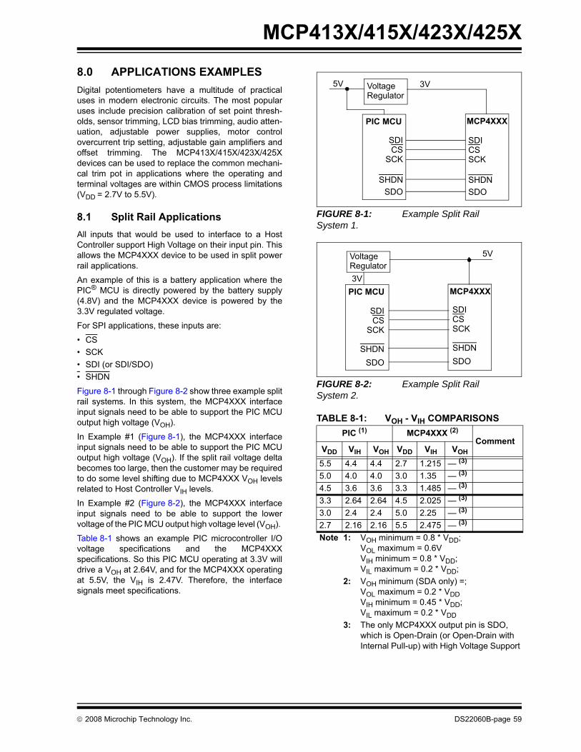
MCP413X/415X/423X/425X
8.0 APPLICATIONS EXAMPLESDigital potentiometers have a multitude of practicaluses in modern electronic circuits. The most popularuses include precision calibration of set point thresh-olds, sensor trimming, LCD bias trimming, audio atten-uation, adjustable power supplies, motor controlovercurrent trip setting, adjustable gain amplifiers andoffset trimming. The MCP413X/415X/423X/425Xdevices can be used to replace the common mechani-cal trim pot in applications where the operating andterminal voltages are within CMOS process limitations(VDD = 2.7V to 5.5V).
8.1 Split Rail ApplicationsAll inputs that would be used to interface to a HostController support High Voltage on their input pin. Thisallows the MCP4XXX device to be used in split powerrail applications.
An example of this is a battery application where thePIC® MCU is directly powered by the battery supply(4.8V) and the MCP4XXX device is powered by the3.3V regulated voltage.
For SPI applications, these inputs are:
• CS • SCK • SDI (or SDI/SDO)• SHDN
Figure 8-1 through Figure 8-2 show three example splitrail systems. In this system, the MCP4XXX interfaceinput signals need to be able to support the PIC MCUoutput high voltage (VOH).
In Example #1 (Figure 8-1), the MCP4XXX interfaceinput signals need to be able to support the PIC MCUoutput high voltage (VOH). If the split rail voltage deltabecomes too large, then the customer may be requiredto do some level shifting due to MCP4XXX VOH levelsrelated to Host Controller VIH levels.
In Example #2 (Figure 8-2), the MCP4XXX interfaceinput signals need to be able to support the lowervoltage of the PIC MCU output high voltage level (VOH).
Table 8-1 shows an example PIC microcontroller I/Ovoltage specifications and the MCP4XXXspecifications. So this PIC MCU operating at 3.3V willdrive a VOH at 2.64V, and for the MCP4XXX operatingat 5.5V, the VIH is 2.47V. Therefore, the interfacesignals meet specifications.
FIGURE 8-1: Example Split Rail System 1.
FIGURE 8-2: Example Split Rail System 2.
TABLE 8-1: VOH - VIH COMPARISONS PIC (1) MCP4XXX (2)
CommentVDD VIH VOH VDD VIH VOH
5.5 4.4 4.4 2.7 1.215 — (3) 5.0 4.0 4.0 3.0 1.35 — (3) 4.5 3.6 3.6 3.3 1.485 — (3) 3.3 2.64 2.64 4.5 2.025 — (3) 3.0 2.4 2.4 5.0 2.25 — (3) 2.7 2.16 2.16 5.5 2.475 — (3) Note 1: VOH minimum = 0.8 * VDD;
VOL maximum = 0.6V VIH minimum = 0.8 * VDD; VIL maximum = 0.2 * VDD;
2: VOH minimum (SDA only) =; VOL maximum = 0.2 * VDD VIH minimum = 0.45 * VDD; VIL maximum = 0.2 * VDD
3: The only MCP4XXX output pin is SDO, which is Open-Drain (or Open-Drain with Internal Pull-up) with High Voltage Support
VoltageRegulator
5V 3V
PIC MCU MCP4XXX
SDICS SCK
SHDN
SDICS
SCK
SHDNSDOSDO
VoltageRegulator3V
5V
PIC MCU MCP4XXX
SDICS SCK
SHDN
SDICS
SCK
SHDNSDOSDO
© 2008 Microchip Technology Inc. DS22060B-page 59

MCP413X/415X/423X/425X
8.2 Techniques to force the CS pin toVIHH The circuit in Figure 8-3 shows a method using theTC1240A doubling charge pump. When the SHDN pinis high, the TC1240A is off, and the level on the CS pinis controlled by the PIC® microcontrollers (MCUs) IO2pin.
When the SHDN pin is low, the TC1240A is on and theVOUT voltage is 2 * VDD. The resistor R1 allows the CSpin to go higher than the voltage such that the PICMCU’s IO2 pin “clamps” at approximately VDD.
FIGURE 8-3: Using the TC1240A to generate the VIHH voltage.The circuit in Figure 8-4 shows the method used on theMCP402X Non-volatile Digital Potentiometer Evalua-tion Board (Part Number: MCP402XEV). This methodrequires that the system voltage be approximately 5V.This ensures that when the PIC10F206 enters abrown-out condition, there is an insufficient voltagelevel on the CS pin to change the stored value of thewiper. The MCP402X Non-volatile DigitalPotentiometer Evaluation Board User’s Guide(DS51546) contains a complete schematic.
GP0 is a general purpose I/O pin, while GP2 can eitherbe a general purpose I/O pin or it can output the internalclock.
For the serial commands, configure the GP2 pin as aninput (high-impedance). The output state of the GP0pin will determine the voltage on the CS pin (VIL or VIH).
For high-voltage serial commands, force the GP0output pin to output a high level (VOH) and configure theGP2 pin to output the internal clock. This will form acharge pump and increase the voltage on the CS pin(when the system voltage is approximately 5V).
FIGURE 8-4: MCP4XXX Non-Volatile Digital Potentiometer Evaluation Board (MCP402XEV) implementation to generate the VIHH voltage.
8.3 Using Shutdown ModesFigure 8-5 shows a possible application circuit wherethe independent terminals could be used.Disconnecting the wiper allows the transistor input tobe taken to the Bias voltage level (disconnecting A andor B may be desired to reduce system current).Disconnecting Terminal A modifies the transistor inputby the RBW rheostat value to the Common B.Disconnecting Terminal B modifies the transistor inputby the RAW rheostat value to the Common A. TheCommon A and Common B connections could beconnected to VDD and VSS.
FIGURE 8-5: Example Application Circuit using Terminal Disconnects.
CS
PIC MCU
MCP402X R1
IO1
IO2 C2
TC1240A VIN SHDN
C+C-
VOUT
C1
CS
PIC10F206
MCP4XXX
R1 GP0
GP2
C2 C1
Balance Bias
W
BInput
Input
To baseof Transistor(or Amplifier)
A
Common B
Common A
DS22060B-page 60 © 2008 Microchip Technology Inc.
MCP413X/415X/423X/425X
8.4 Design ConsiderationsIn the design of a system with the MCP4XXX devices,the following considerations should be taken intoaccount:• Power Supply Considerations• Layout Considerations
8.4.1 POWER SUPPLY CONSIDERATIONS
The typical application will require a bypass capacitorin order to filter high-frequency noise, which can beinduced onto the power supply's traces. The bypasscapacitor helps to minimize the effect of these noisesources on signal integrity. Figure 8-6 illustrates anappropriate bypass strategy.
In this example, the recommended bypass capacitorvalue is 0.1 µF. This capacitor should be placed asclose (within 4 mm) to the device power pin (VDD) aspossible.
The power source supplying these devices should beas clean as possible. If the application circuit hasseparate digital and analog power supplies, VDD andVSS should reside on the analog plane.
FIGURE 8-6: Typical Microcontroller Connections.
8.4.2 LAYOUT CONSIDERATIONSInductively-coupled AC transients and digital switchingnoise can degrade the input and output signal integrity,potentially masking the MCP4XXX’s performance.Careful board layout minimizes these effects andincreases the Signal-to-Noise Ratio (SNR). Multi-layerboards utilizing a low-inductance ground plane,isolated inputs, isolated outputs and proper decouplingare critical to achieving the performance that the siliconis capable of providing. Particularly harshenvironments may require shielding of critical signals.
If low noise is desired, breadboards and wire-wrappedboards are not recommended.
8.4.3 RESISTOR TEMPCO Characterization curves of the resistor temperaturecoefficient (Tempco) are shown in Figure 2-11,Figure 2-24, Figure 2-36, and Figure 2-48.
These curves show that the resistor network isdesigned to correct for the change in resistance astemperature increases. This technique reduces theend to end change is RAB resistance.
8.4.4 HIGH VOLTAGE TOLERANT PINSHigh Voltage support (VIHH) on the Serial Interface pinssupports two features. These are:
• In-Circuit Accommodation of split rail applications and power supply sync issues
• Compatability with systems that also support MCP414X/416X /424X/426X devicesVDD
VDD
VSS VSS
MC
P413
X/41
5X/
423X
/425
X
0.1 µF
PIC
® M
icro
cont
rolle
r
0.1 µF
U/D
CS
W
B
A
© 2008 Microchip Technology Inc. DS22060B-page 61
MCP413X/415X/423X/425X
NOTES:DS22060B-page 62 © 2008 Microchip Technology Inc.
MCP413X/415X/423X/425X
9.0 DEVELOPMENT SUPPORT
9.1 Development ToolsSeveral development tools are available to assist inyour design and evaluation of the MCP4XXX devices.The currently available tools are shown in Table 9-1.
These boards may be purchased directly from theMicrochip web site at www.microchip.com.
9.2 Technical DocumentationSeveral additional technical documents are available toassist you in your design and development. Thesetechnical documents include Application Notes,Technical Briefs, and Design Guides. Table 9-2 showssome of these documents.
TABLE 9-1: DEVELOPMENT TOOLS
TABLE 9-2: TECHNICAL DOCUMENTATION
Board Name Part # Supported DevicesMCP42XX Digital Potentiometer PICtail Plus DemoBoard
MCP42XXDM-PTPLS MCP42XX
MCP4XXX Digital Potentiometer Daughter Board (1) MCP4XXXDM-DB MCP42XXX, MCP42XX, MCP4021, and MCP4011
8-pin SOIC/MSOP/TSSOP/DIP Evaluation Board SOIC8EV Any 8-pin device in DIP, SOIC,MSOP, or TSSOP package
14-pin SOIC/MSOP/DIP Evaluation Board SOIC14EV Any 14-pin device in DIP, SOIC, orMSOP package
Note 1: Requires the use of a PICDEM Demo board (see User’s Guide for details)
ApplicationNote Number
Title Literature #
AN1080 Understanding Digital Potentiometers Resistor Variations DS01080AN737 Using Digital Potentiometers to Design Low Pass Adjustable Filters DS00737AN692 Using a Digital Potentiometer to Optimize a Precision Single Supply Photo Detect DS00692AN691 Optimizing the Digital Potentiometer in Precision Circuits DS00691AN219 Comparing Digital Potentiometers to Mechanical Potentiometers DS00219— Digital Potentiometer Design Guide DS22017— Signal Chain Design Guide DS21825
© 2008 Microchip Technology Inc. DS22060B-page 63

MCP413X/415X/423X/425X
NOTES:DS22060B-page 64 © 2008 Microchip Technology Inc.
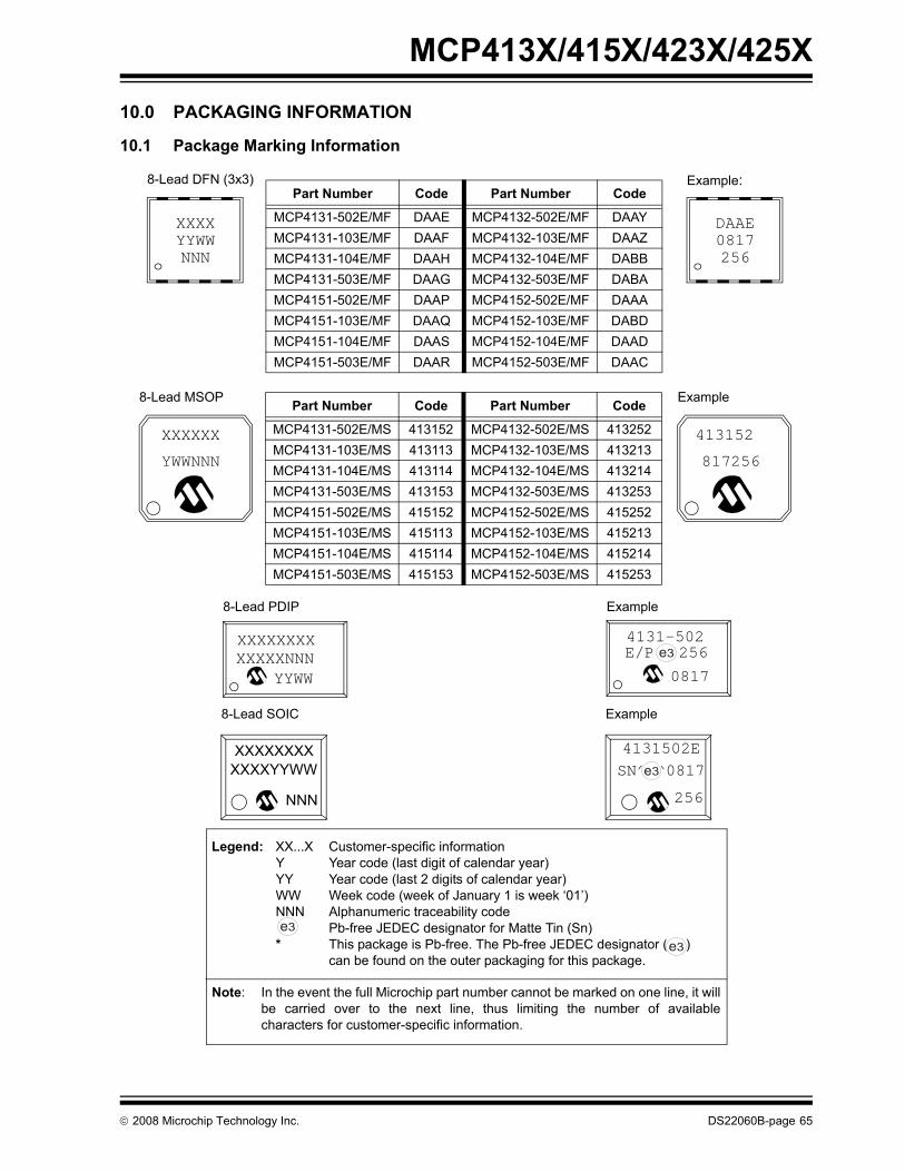
MCP413X/415X/423X/425X
10.0 PACKAGING INFORMATION
10.1 Package Marking Information
Legend: XX...X Customer-specific informationY Year code (last digit of calendar year)YY Year code (last 2 digits of calendar year)WW Week code (week of January 1 is week ‘01’)NNN Alphanumeric traceability code Pb-free JEDEC designator for Matte Tin (Sn)* This package is Pb-free. The Pb-free JEDEC designator ( )
can be found on the outer packaging for this package.
Note: In the event the full Microchip part number cannot be marked on one line, it willbe carried over to the next line, thus limiting the number of availablecharacters for customer-specific information.
3e
3e
8-Lead DFN (3x3) Example:Part Number Code Part Number Code
MCP4131-502E/MF DAAE MCP4132-502E/MF DAAYMCP4131-103E/MF DAAF MCP4132-103E/MF DAAZMCP4131-104E/MF DAAH MCP4132-104E/MF DABBMCP4131-503E/MF DAAG MCP4132-503E/MF DABAMCP4151-502E/MF DAAP MCP4152-502E/MF DAAAMCP4151-103E/MF DAAQ MCP4152-103E/MF DABDMCP4151-104E/MF DAAS MCP4152-104E/MF DAADMCP4151-503E/MF DAAR MCP4152-503E/MF DAAC
DAAE0817256
XXXXYYWWNNN
8-Lead MSOP
XXXXXX
YWWNNN
Example
413152
817256
Part Number Code Part Number Code
MCP4131-502E/MS 413152 MCP4132-502E/MS 413252MCP4131-103E/MS 413113 MCP4132-103E/MS 413213MCP4131-104E/MS 413114 MCP4132-104E/MS 413214MCP4131-503E/MS 413153 MCP4132-503E/MS 413253MCP4151-502E/MS 415152 MCP4152-502E/MS 415252MCP4151-103E/MS 415113 MCP4152-103E/MS 415213MCP4151-104E/MS 415114 MCP4152-104E/MS 415214MCP4151-503E/MS 415153 MCP4152-503E/MS 415253
XXXXXNNN
8-Lead PDIP
XXXXXXXX
YYWW
E/P 256
Example
4131-502
0817
3e
8-Lead SOIC
XXXXXXXXXXXXYYWW
NNN
Example
4131502ESN^^^0817
256
3e
© 2008 Microchip Technology Inc. DS22060B-page 65
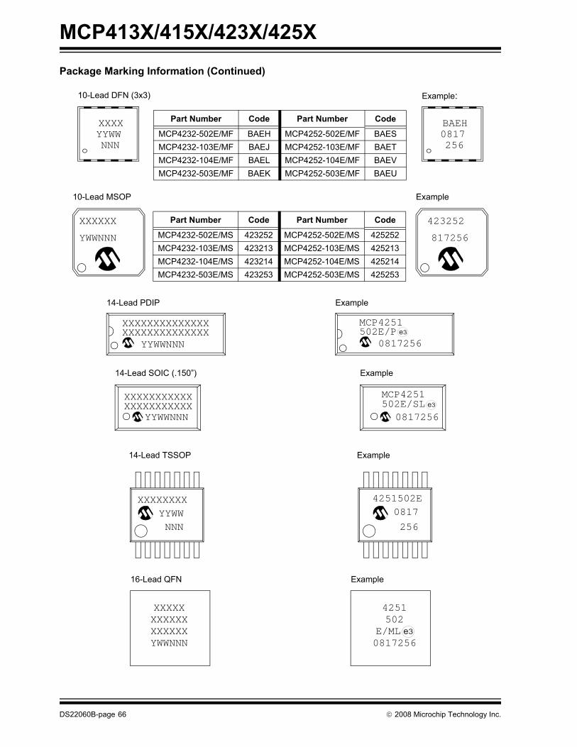
MCP413X/415X/423X/425X
Package Marking Information (Continued)10-Lead DFN (3x3) Example:
Part Number Code Part Number Code
MCP4232-502E/MF BAEH MCP4252-502E/MF BAESMCP4232-103E/MF BAEJ MCP4252-103E/MF BAETMCP4232-104E/MF BAEL MCP4252-104E/MF BAEVMCP4232-503E/MF BAEK MCP4252-503E/MF BAEU
BAEH0817256
XXXXYYWWNNN
10-Lead MSOP
XXXXXX
YWWNNN
Example
423252
817256
Part Number Code Part Number Code
MCP4232-502E/MS 423252 MCP4252-502E/MS 425252MCP4232-103E/MS 423213 MCP4252-103E/MS 425213MCP4232-104E/MS 423214 MCP4252-104E/MS 425214MCP4232-503E/MS 423253 MCP4252-503E/MS 425253
14-Lead TSSOP
XXXXXXXXYYWWNNN
Example
4251502E0817
256
XXXXX
16-Lead QFN
XXXXXX
YWWNNN
Example
14-Lead SOIC (.150”)
XXXXXXXXXXXXXXXXXXXXXX
YYWWNNN
Example
MCP4251502E/SL^^
08172563e
XXXXXX
4251502
0817256E/ML^ 3e
14-Lead PDIP
XXXXXXXXXXXXXXXXXXXXXXXXXXXX
YYWWNNN
Example
MCP4251502E/P^^
08172563e
DS22060B-page 66 © 2008 Microchip Technology Inc.
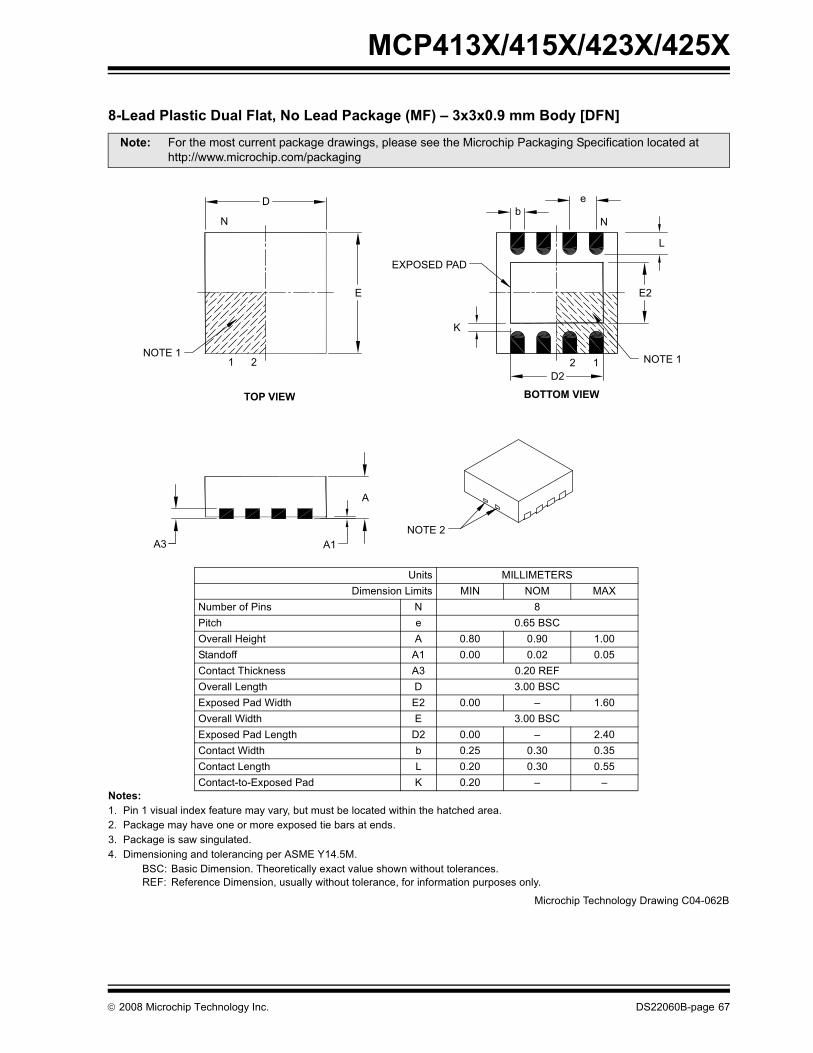
MCP413X/415X/423X/425X
!"#$
% !" #$ %! &'(!%&! %( % ")%% % " * & & # "% ( % " + * ) !% " & "% ,-.
/01 / & % #%! ))%!%% ,21 $ & '! !)%!%% '$$&%!
% 2% & %! %* ") ' % * $%% "%%%133)))&&3*
4% 55,,& 5&% 6 67 8
6!&( $ 6 9% :./07 ; % 9 %"$$ .0%%* + ,27 5 % +/0,# ""<"% , = :7 <"% , +/0,# ""5 % = 0%%<"% ( . + +.0%%5 % 5 + ..0%%%,# "" > = =
BOTTOM VIEWTOP VIEW
D
N
E
NOTE 11 2
EXPOSED PAD
be
N
L
E2
K
NOTE 1D2
2 1
NOTE 2
A
A1A3
) 0:/
© 2008 Microchip Technology Inc. DS22060B-page 67

MCP413X/415X/423X/425X
!"#$
% 2% & %! %* ") ' % * $%% "%%%133)))&&3*
DS22060B-page 68 © 2008 Microchip Technology Inc.
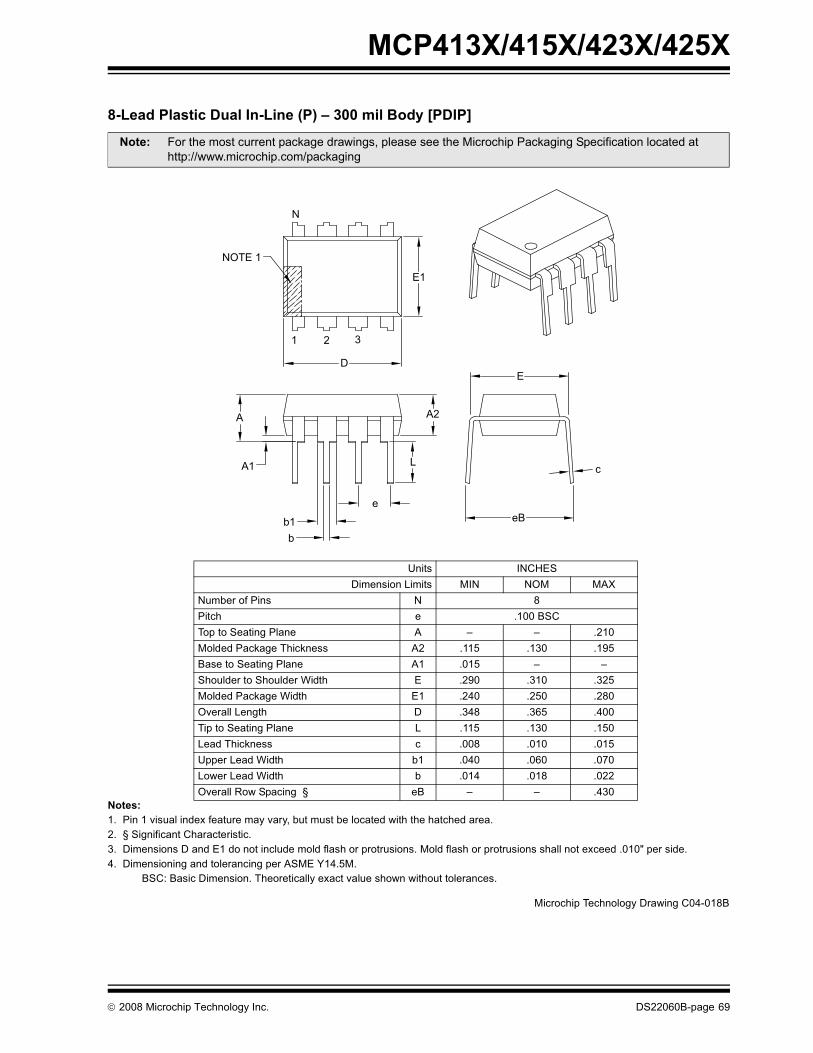
MCP413X/415X/423X/425X
&' ' !"#&$
% !" #$ %! &'(!%&! %( % ")%% % " ?$%0% %+ & ","%!" &"$ %! "$ %! % # "@ " & "% ,-.
/01/ & % #%! ))%!%%
% 2% & %! %* ") ' % * $%% "%%%133)))&&3*
4% 60;,& 5&% 6 67 8
6!&( $ 6 9% /0% % = = " "* * . + ./ % % . = =!" %!" <"% , + +." "* <"% , . 97 5 % +9 +:. % % 5 . + .5 "* 9 .4 5 "<"% ( : 5) 5 "<"% ( 9 7 )? / = = +
N
E1
NOTE 1
D
1 2 3
A
A1
A2
L
b1b
e
E
eB
c
) 09/
© 2008 Microchip Technology Inc. DS22060B-page 69

MCP413X/415X/423X/425X
() * ')#)*$
% !" #$ %! &'(!%&! %( % ")%% % " & ","%!" &"$ %! "$ %! % # ".&& " + & "% ,-.
/01 / & % #%! ))%!%% ,21 $ & '! !)%!%% '$$&%!
% 2% & %! %* ") ' % * $%% "%%%133)))&&3*
4% 55,,& 5&% 6 67 8
6!&( $ 6 9% :./07 ; % = = " "* * . 9. .%"$$ = .7 <"% , /0" "* <"% , +/07 5 % +/02%5 % 5 : 92%% 5 .,22% A = 9A5 "* 9 = +5 "<"% ( =
D
N
E
E1
NOTE 1
1 2e
b
A
A1
A2c
L1 L
φ
) 0/
DS22060B-page 70 © 2008 Microchip Technology Inc.
MCP413X/415X/423X/425X
) * ')((+ !"#)*&,$
% !" #$ %! &'(!%&! %( % ")%% % " ?$%0% %+ & ","%!" &"$ %! "$ %! % # ".&& " & "% ,-.
/01 / & % #%! ))%!%% ,21 $ & '! !)%!%% '$$&%!
% 2% & %! %* ") ' % * $%% "%%%133)))&&3*
4% 55,,& 5&% 6 67 8
6!&( $ 6 9% /07 ; % = = ." "* * . = =%"$$? = .7 <"% , :/0" "* <"% , +/07 5 % /00&$ B%C . = .2%5 % 5 = 2%% 5 ,22% A = 9A5 "* = .5 "<"% ( + = ."$% .A = .A"$% /%%& .A = .A
D
Ne
E
E1
NOTE 1
1 2 3
b
A
A1
A2
L
L1
c
h
h
φ
β
α
) 0./
© 2008 Microchip Technology Inc. DS22060B-page 71

MCP413X/415X/423X/425X
) * ')((+ !"#)*&,$
% 2% & %! %* ") ' % * $%% "%%%133)))&&3*
DS22060B-page 72 © 2008 Microchip Technology Inc.

MCP413X/415X/423X/425X
- !"#$
% !" #$ %! &'(!%&! %( % ")%% % " * & & # "% ( % " + * ) !% " & "% ,-.
/01 / & % #%! ))%!%% ,21 $ & '! !)%!%% '$$&%!
% 2% & %! %* ") ' % * $%% "%%%133)))&&3*
4% 55,,& 5&% 6 67 8
6!&( $ 6 % ./07 ; % 9 %"$$ .0%%* + ,27 5 % +/0,# ""5 % +. 97 <"% , +/0,# ""<"% , .9 .0%%<"% ( 9 . +0%%5 % 5 + .0%%%,# "" > = =
D
N
NOTE 1 1 2
E
be
N
L
E2
NOTE 112
D2
K
EXPOSEDPAD
BOTTOM VIEWTOP VIEW
A3 A1
A
NOTE 2
) 0:+/
© 2008 Microchip Technology Inc. DS22060B-page 73

MCP413X/415X/423X/425X
- !"#$
% 2% & %! %* ") ' % * $%% "%%%133)))&&3*
DS22060B-page 74 © 2008 Microchip Technology Inc.

MCP413X/415X/423X/425X
- () * '.#)*$
% !" #$ %! &'(!%&! %( % ")%% % " & ","%!" &"$ %! "$ %! % # ".&& " + & "% ,-.
/01 / & % #%! ))%!%% ,21 $ & '! !)%!%% '$$&%!
% 2% & %! %* ") ' % * $%% "%%%133)))&&3*
4% 55,,& 5&% 6 67 8
6!&( $ 6 % ./07 ; % = = " "* * . 9. .%"$$ = .7 <"% , /0" "* <"% , +/07 5 % +/02%5 % 5 : 92%% 5 .,22% A = 9A5 "* 9 = +5 "<"% ( . = ++
D
E
E1
N
NOTE 1
1 2b
e
A
A1
A2 c
L
L1
φ
) 0/
© 2008 Microchip Technology Inc. DS22060B-page 75
MCP413X/415X/423X/425X
-/ &' ' !"#&$
% !" #$ %! &'(!%&! %( % ")%% % " ?$%0% %+ & ","%!" &"$ %! "$ %! % # "@ " & "% ,-.
/01/ & % #%! ))%!%%
% 2% & %! %* ") ' % * $%% "%%%133)))&&3*
4% 60;,& 5&% 6 67 8
6!&( $ 6 % /0% % = = " "* * . + ./ % % . = =!" %!" <"% , + +." "* <"% , . 97 5 % +. . .% % 5 . + .5 "* 9 .4 5 "<"% ( . : 5) 5 "<"% ( 9 7 )? / = = +
N
E1
D
NOTE 1
1 2 3
E
c
eB
A2
L
A
A1b1
b e
) 0./
DS22060B-page 76 © 2008 Microchip Technology Inc.

MCP413X/415X/423X/425X
-/ ) * ')((+ !"#)*&,$
% !" #$ %! &'(!%&! %( % ")%% % " ?$%0% %+ & ","%!" &"$ %! "$ %! % # ".&& " & "% ,-.
/01 / & % #%! ))%!%% ,21 $ & '! !)%!%% '$$&%!
% 2% & %! %* ") ' % * $%% "%%%133)))&&3*
4% 55,,& 5&% 6 67 8
6!&( $ 6 % /07 ; % = = ." "* * . = =%"$$? = .7 <"% , :/0" "* <"% , +/07 5 % 9:./00&$ B%C . = .2%5 % 5 = 2%% 5 ,22% A = 9A5 "* = .5 "<"% ( + = ."$% .A = .A"$% /%%& .A = .A
NOTE 1
N
D
E
E1
1 2 3
b
e
A
A1
A2
L
L1
c
h
h α
β
φ
) 0:./
© 2008 Microchip Technology Inc. DS22060B-page 77

MCP413X/415X/423X/425X
% 2% & %! %* ") ' % * $%% "%%%133)))&&3*
DS22060B-page 78 © 2008 Microchip Technology Inc.

MCP413X/415X/423X/425X
-/ 01 ')1( ') * ')0// !"#0))*$
% !" #$ %! &'(!%&! %( % ")%% % " & ","%!" &"$ %! "$ %! % # ".&& " + & "% ,-.
/01 / & % #%! ))%!%% ,21 $ & '! !)%!%% '$$&%!
% 2% & %! %* ") ' % * $%% "%%%133)))&&3*
4% 55,,& 5&% 6 67 8
6!&( $ 6 % :./07 ; % = = " "* * 9 .%"$$ . = .7 <"% , :/0" "* <"% , + ." "* 5 % . .2%5 % 5 . : .2%% 5 ,22% A = 9A5 "* = 5 "<"% ( = +
NOTE 1
D
N
E
E1
1 2
eb
cA
A1
A2
L1 L
φ
) 09/
© 2008 Microchip Technology Inc. DS22060B-page 79

MCP413X/415X/423X/425X
-2 3// !"#3$
% !" #$ %! &'(!%&! %( % ")%% % " * ) !% "+ & "% ,-.
/01 / & % #%! ))%!%% ,21 $ & '! !)%!%% '$$&%!
% 2% & %! %* ") ' % * $%% "%%%133)))&&3*
4% 55,,& 5&% 6 67 8
6!&( $ 6 :% :./07 ; % 9 %"$$ .0%%* + ,27 <"% , /0,# ""<"% , . :. 97 5 % /0,# ""5 % . :. 90%%<"% ( . + +.0%%5 % 5 + .0%%%,# "" > = =
D
E
N
2
1
EXPOSEDPAD
D2
E22
1
e
b
KN
NOTE 1
A3
A1
A
LTOP VIEW BOTTOM VIEW
) 0/
DS22060B-page 80 © 2008 Microchip Technology Inc.

MCP413X/415X/423X/425X
% 2% & %! %* ") ' % * $%% "%%%133)))&&3*
© 2008 Microchip Technology Inc. DS22060B-page 81

MCP413X/415X/423X/425X
NOTES:DS22060B-page 82 © 2008 Microchip Technology Inc.

MCP413X/415X/423X/425X
APPENDIX A: REVISION HISTORY
Revision B (December 2008)The following is the list of modifications:
1. Updated IPU specifications to specify testconditions and new limit.
2. Updated DFN package in “Package Types (topview)”, including Exposed Thermal Pad sample(EP).
3. Added new descriptions in Section 3.0 “PinDescriptions”.
4. Added new Development Tool support items.5. Updated Package Outline section.
Revision A (September 2007)• Original Release of this Document.
APPENDIX B: MIGRATING FROM THE MCP41XXX AND MCP42XXX DEVICES
This is intended to give an overview of some of thedifferences to be aware of when migrating from theMCP41XXX and MCP42XXX devices.
B.1 MCP41XXX to MCP41XX Differences
Here are some of the differences to be aware of:
1. SI pin is now SDI/SDO pin, and the contents ofthe device memory can be read.
2. Need to address the Terminal Connect Feature(TCON register) of MCP41XX.
3. MCP41XX supports software Shutdown mode.4. New 5 kΩ version.5. MCP41XX have 7-bit resolution options.6. Alternate pinout versions (for Rheostat
configuration).7. Verify device’s electrical specifications.8. Interface signals are now high voltage tolerant.9. Interface signals now have internal pull-up
resistors.
B.2 MCP42XXX to MCP42XX Differences
Here are some of the differences to be aware of:
1. Daisy chaining of devices is no longersupported.
2. SDO pin allows contents of device memory to beread.
3. Need to address the Terminal Connect Feature(TCON register) of MCP42XX.
4. MCP42XX supports software Shutdown mode.5. New 5 kΩ version.6. MCP42XX have 7-bit resolution options.7. Alternate package/pinout versions (for Rheostat
configuration).8. Verify device’s electrical specifications.9. Interface signals are now high voltage tolerant10. Interface signals now have internal pull-up
resistors.
© 2008 Microchip Technology Inc. DS22060B-page 83

MCP413X/415X/423X/425X
NOTES:DS22060B-page 84 © 2008 Microchip Technology Inc.

MCP413X/415X/423X/425X
PRODUCT IDENTIFICATION SYSTEMTo order or obtain information, e.g., on pricing or delivery, refer to the factory or the listed sales office.PART NO. X /XXXXX
Resistance PackageTemperatureRange
Device
Device MCP4131: Single Volatile 7-bit PotentiometerMCP4131T: Single Volatile 7-bit Potentiometer
(Tape and Reel)MCP4132: Single Volatile 7-bit RheostatMCP4132T: Single Volatile 7-bit Rheostat
(Tape and Reel)MCP4151: Single Volatile 8-bit PotentiometerMCP4151T: Single Volatile 8-bit Potentiometer
(Tape and Reel)MCP4152: Single Volatile 8-bit RheostatMCP4152T: Single Volatile 8-bit Rheostat
(Tape and Reel)MCP4231: Dual Volatile 7-bit PotentiometerMCP4231T: Dual Volatile 7-bit Potentiometer
(Tape and Reel)MCP4232: Dual Volatile 7-bit RheostatMCP4232T: Dual Volatile 7-bit Rheostat
(Tape and Reel)MCP4251: Dual Volatile 8-bit PotentiometerMCP4251T: Dual Volatile 8-bit Potentiometer
(Tape and Reel)MCP4252: Dual Volatile 8-bit RheostatMCP4252T: Dual Volatile 8-bit Rheostat
(Tape and Reel)
Resistance Version: 502 = 5 kΩ103 = 10 kΩ503 = 50 kΩ104 = 100 kΩ
Temperature Range I = -40°C to +85°C (Industrial)E = -40°C to +125°C (Extended)
Package MF = Plastic Dual Flat No-lead (3x3 DFN), 8/10-leadML = Plastic Quad Flat No-lead (QFN), 16-leadMS = Plastic Micro Small Outline (MSOP), 8-leadP = Plastic Dual In-line (PDIP) (300 mil), 8/14-lead SN = Plastic Small Outline (SOIC), (150 mil), 8-leadSL = Plastic Small Outline (SOIC), (150 mil), 14-leadST = Plastic Thin Shrink Small Outline (TSSOP), 14-leadUN = Plastic Micro Small Outline (MSOP), 10-lead
Examples:a) MCP4131-502E/XX: 5 kΩ, 8LD Deviceb) MCP4131T-502E/XX: T/R, 5 kΩ, 8LD Devicec) MCP4131-103E/XX: 10 kΩ, 8-LD Deviced) MCP4131T-103E/XX: T/R, 10 kΩ, 8LD Devicee) MCP4131-503E/XX: 50 kΩ, 8LD Devicef) MCP4131T-503E/XX: T/R, 50 kΩ, 8LD Deviceg) MCP4131-104E/XX: 100 kΩ, 8LD Deviceh) MCP4131T-104E/XX: T/R, 100 kΩ, 8LD Device
a) MCP4132-502E/XX: 5 kΩ, 8LD Deviceb) MCP4132T-502E/XX: T/R, 5 kΩ, 8LD Devicec) MCP4132-103E/XX: 10 kΩ, 8-LD Deviced) MCP4132T-103E/XX: T/R, 10 kΩ, 8LD Devicee) MCP4132-503E/XX: 50 kΩ, 8LD Devicef) MCP4132T-503E/XX: T/R, 50 kΩ, 8LD Deviceg) MCP4132-104E/XX: 100 kΩ, 8LD Deviceh) MCP4132T-104E/XX: T/R, 100 kΩ, 8LD Device
a) MCP4151-502E/XX: 5 kΩ, 8LD Deviceb) MCP4151T-502E/XX: T/R, 5 kΩ, 8LD Devicec) MCP4151-103E/XX: 10 kΩ, 8-LD Deviced) MCP4151T-103E/XX: T/R, 10 kΩ, 8LD Devicee) MCP4151-503E/XX: 50 kΩ, 8LD Devicef) MCP4151T-503E/XX: T/R, 50 kΩ, 8LD Deviceg) MCP4151-104E/XX: 100 kΩ, 8LD Deviceh) MCP4151T-104E/XX: T/R, 100 kΩ, 8LD Device
a) MCP4152-502E/XX: 5 kΩ, 8LD Deviceb) MCP4152T-502E/XX: T/R, 5 kΩ, 8LD Devicec) MCP4152-103E/XX: 10 kΩ, 8-LD Deviced) MCP4152T-103E/XX: T/R, 10 kΩ, 8LD Devicee) MCP4152-503E/XX: 50 kΩ, 8LD Devicef) MCP4152T-503E/XX: T/R, 50 kΩ, 8LD Deviceg) MCP4152-104E/XX: 100 kΩ, 8LD Deviceh) MCP4152T-104E/XX: T/R, 100 kΩ, 8LD Device
a) MCP4231-502E/XX: 5 kΩ, 8LD Deviceb) MCP4231T-502E/XX: T/R, 5 kΩΩ, 8LD Devicec) MCP4231-103E/XX: 10 kΩ, 8-LD Deviced) MCP4231T-103E/XX: T/R, 10 kΩ, 8LD Devicee) MCP4231-503E/XX: 50 kΩ, 8LD Devicef) MCP4231T-503E/XX: T/R, 50 kΩ, 8LD Deviceg) MCP4231-104E/XX: 100 kΩ, 8LD Deviceh) MCP4231T-104E/XX: T/R, 100 kΩ, 8LD Device
a) MCP4232-502E/XX: 5 kΩ, 8LD Deviceb) MCP4232T-502E/XX: T/R, 5 kΩ, 8LD Devicec) MCP4232-103E/XX: 10 kΩ, 8-LD Deviced) MCP4232T-103E/XX: T/R, 10 kΩ, 8LD Devicee) MCP4232-503E/XX: 50 kΩ, 8LD Devicef) MCP4232T-503E/XX: T/R, 50 kΩ, 8LD Deviceg) MCP4232-104E/XX: 100 kΩ, 8LD Deviceh) MCP4232T-104E/XX: T/R, 100 kΩ, 8LD Device
a) MCP4251-502E/XX: 5 kΩ, 8LD Deviceb) MCP4251T-502E/XX: T/R, 5 kΩ, 8LD Devicec) MCP4251-103E/XX: 10 kΩ, 8-LD Deviced) MCP4251T-103E/XX: T/R, 10 kΩ, 8LD Devicee) MCP4251-503E/XX: 50 kΩ, 8LD Devicef) MCP4251T-503E/XX: T/R, 50 kΩ, 8LD Deviceg) MCP4251-104E/XX: 100 kΩ, 8LD Deviceh) MCP4251T-104E/XX: T/R, 100 kΩ, 8LD Device
a) MCP4252-502E/XX: 5 kΩ, 8LD Deviceb) MCP4252T-502E/XX: T/R, 5 kΩ, 8LD Devicec) MCP4252-103E/XX: 10 kΩ, 8-LD Deviced) MCP4252T-103E/XX: T/R, 10 kΩ, 8LD Devicee) MCP4252-503E/XX: 50 kΩ, 8LD Devicef) MCP4252T-503E/XX: T/R, 50 kΩ, 8LD Deviceg) MCP4252-104E/XX: 100 kΩ, 8LD Deviceh) MCP4252T-104E/XX: T/R, 100 kΩ, 8LD DeviceXX = MF for 8/10-lead 3x3 DFN
= ML for 16-lead QFN= MS for 8-lead MSOP= P for 8/14-lead PDIP= SN for 8-lead SOIC= SL for 14-lead SOIC= ST for 14-lead TSSOP= UN for 10-lead MSOP
Version
© 2008 Microchip Technology Inc. DS22060B-page 85

MCP413X/415X/423X/425X
NOTES:DS22060B-page 86 © 2008 Microchip Technology Inc.

Note the following details of the code protection feature on Microchip devices:• Microchip products meet the specification contained in their particular Microchip Data Sheet.
• Microchip believes that its family of products is one of the most secure families of its kind on the market today, when used in the intended manner and under normal conditions.
• There are dishonest and possibly illegal methods used to breach the code protection feature. All of these methods, to our knowledge, require using the Microchip products in a manner outside the operating specifications contained in Microchip’s Data Sheets. Most likely, the person doing so is engaged in theft of intellectual property.
• Microchip is willing to work with the customer who is concerned about the integrity of their code.
• Neither Microchip nor any other semiconductor manufacturer can guarantee the security of their code. Code protection does not mean that we are guaranteeing the product as “unbreakable.”
Code protection is constantly evolving. We at Microchip are committed to continuously improving the code protection features of ourproducts. Attempts to break Microchip’s code protection feature may be a violation of the Digital Millennium Copyright Act. If such actsallow unauthorized access to your software or other copyrighted work, you may have a right to sue for relief under that Act.
Information contained in this publication regarding deviceapplications and the like is provided only for your convenienceand may be superseded by updates. It is your responsibility toensure that your application meets with your specifications.MICROCHIP MAKES NO REPRESENTATIONS ORWARRANTIES OF ANY KIND WHETHER EXPRESS ORIMPLIED, WRITTEN OR ORAL, STATUTORY OROTHERWISE, RELATED TO THE INFORMATION,INCLUDING BUT NOT LIMITED TO ITS CONDITION,QUALITY, PERFORMANCE, MERCHANTABILITY ORFITNESS FOR PURPOSE. Microchip disclaims all liabilityarising from this information and its use. Use of Microchipdevices in life support and/or safety applications is entirely atthe buyer’s risk, and the buyer agrees to defend, indemnify andhold harmless Microchip from any and all damages, claims,suits, or expenses resulting from such use. No licenses areconveyed, implicitly or otherwise, under any Microchipintellectual property rights.
© 2008 Microchip Technology Inc.
Trademarks
The Microchip name and logo, the Microchip logo, Accuron, dsPIC, KEELOQ, KEELOQ logo, MPLAB, PIC, PICmicro, PICSTART, rfPIC, SmartShunt and UNI/O are registered trademarks of Microchip Technology Incorporated in the U.S.A. and other countries.
FilterLab, Linear Active Thermistor, MXDEV, MXLAB, SEEVAL, SmartSensor and The Embedded Control Solutions Company are registered trademarks of Microchip Technology Incorporated in the U.S.A.
Analog-for-the-Digital Age, Application Maestro, CodeGuard, dsPICDEM, dsPICDEM.net, dsPICworks, dsSPEAK, ECAN, ECONOMONITOR, FanSense, In-Circuit Serial Programming, ICSP, ICEPIC, Mindi, MiWi, MPASM, MPLAB Certified logo, MPLIB, MPLINK, mTouch, PICkit, PICDEM, PICDEM.net, PICtail, PIC32 logo, PowerCal, PowerInfo, PowerMate, PowerTool, REAL ICE, rfLAB, Select Mode, Total Endurance, WiperLock and ZENA are trademarks of Microchip Technology Incorporated in the U.S.A. and other countries.
SQTP is a service mark of Microchip Technology Incorporated in the U.S.A.
All other trademarks mentioned herein are property of their respective companies.
© 2008, Microchip Technology Incorporated, Printed in the U.S.A., All Rights Reserved.
Printed on recycled paper.
DS22060B-page 87
Microchip received ISO/TS-16949:2002 certification for its worldwide headquarters, design and wafer fabrication facilities in Chandler and Tempe, Arizona; Gresham, Oregon and design centers in California and India. The Company’s quality system processes and procedures are for its PIC® MCUs and dsPIC® DSCs, KEELOQ® code hopping devices, Serial EEPROMs, microperipherals, nonvolatile memory and analog products. In addition, Microchip’s quality system for the design and manufacture of development systems is ISO 9001:2000 certified.

DS22060B-page 88 © 2008 Microchip Technology Inc.
AMERICASCorporate Office2355 West Chandler Blvd.Chandler, AZ 85224-6199Tel: 480-792-7200 Fax: 480-792-7277Technical Support: http://support.microchip.comWeb Address: www.microchip.comAtlantaDuluth, GA Tel: 678-957-9614 Fax: 678-957-1455BostonWestborough, MA Tel: 774-760-0087 Fax: 774-760-0088ChicagoItasca, IL Tel: 630-285-0071 Fax: 630-285-0075DallasAddison, TX Tel: 972-818-7423 Fax: 972-818-2924DetroitFarmington Hills, MI Tel: 248-538-2250Fax: 248-538-2260KokomoKokomo, IN Tel: 765-864-8360Fax: 765-864-8387Los AngelesMission Viejo, CA Tel: 949-462-9523 Fax: 949-462-9608Santa ClaraSanta Clara, CA Tel: 408-961-6444Fax: 408-961-6445TorontoMississauga, Ontario, CanadaTel: 905-673-0699 Fax: 905-673-6509
ASIA/PACIFICAsia Pacific OfficeSuites 3707-14, 37th FloorTower 6, The GatewayHarbour City, KowloonHong KongTel: 852-2401-1200Fax: 852-2401-3431Australia - SydneyTel: 61-2-9868-6733Fax: 61-2-9868-6755China - BeijingTel: 86-10-8528-2100 Fax: 86-10-8528-2104China - ChengduTel: 86-28-8665-5511Fax: 86-28-8665-7889China - Hong Kong SARTel: 852-2401-1200 Fax: 852-2401-3431China - NanjingTel: 86-25-8473-2460Fax: 86-25-8473-2470China - QingdaoTel: 86-532-8502-7355Fax: 86-532-8502-7205China - ShanghaiTel: 86-21-5407-5533 Fax: 86-21-5407-5066China - ShenyangTel: 86-24-2334-2829Fax: 86-24-2334-2393China - ShenzhenTel: 86-755-8203-2660 Fax: 86-755-8203-1760China - WuhanTel: 86-27-5980-5300Fax: 86-27-5980-5118China - XiamenTel: 86-592-2388138 Fax: 86-592-2388130China - XianTel: 86-29-8833-7252Fax: 86-29-8833-7256China - ZhuhaiTel: 86-756-3210040 Fax: 86-756-3210049
ASIA/PACIFICIndia - BangaloreTel: 91-80-4182-8400 Fax: 91-80-4182-8422India - New DelhiTel: 91-11-4160-8631Fax: 91-11-4160-8632India - PuneTel: 91-20-2566-1512Fax: 91-20-2566-1513Japan - YokohamaTel: 81-45-471- 6166 Fax: 81-45-471-6122Korea - DaeguTel: 82-53-744-4301Fax: 82-53-744-4302Korea - SeoulTel: 82-2-554-7200Fax: 82-2-558-5932 or 82-2-558-5934Malaysia - Kuala LumpurTel: 60-3-6201-9857Fax: 60-3-6201-9859Malaysia - PenangTel: 60-4-227-8870Fax: 60-4-227-4068Philippines - ManilaTel: 63-2-634-9065Fax: 63-2-634-9069SingaporeTel: 65-6334-8870Fax: 65-6334-8850Taiwan - Hsin ChuTel: 886-3-572-9526Fax: 886-3-572-6459Taiwan - KaohsiungTel: 886-7-536-4818Fax: 886-7-536-4803Taiwan - TaipeiTel: 886-2-2500-6610 Fax: 886-2-2508-0102Thailand - BangkokTel: 66-2-694-1351Fax: 66-2-694-1350
EUROPEAustria - WelsTel: 43-7242-2244-39Fax: 43-7242-2244-393Denmark - CopenhagenTel: 45-4450-2828 Fax: 45-4485-2829France - ParisTel: 33-1-69-53-63-20 Fax: 33-1-69-30-90-79Germany - MunichTel: 49-89-627-144-0 Fax: 49-89-627-144-44Italy - Milan Tel: 39-0331-742611 Fax: 39-0331-466781Netherlands - DrunenTel: 31-416-690399 Fax: 31-416-690340Spain - MadridTel: 34-91-708-08-90Fax: 34-91-708-08-91UK - WokinghamTel: 44-118-921-5869Fax: 44-118-921-5820
WORLDWIDE SALES AND SERVICE
01/02/08
Related Documents