1. General description The 74HC4017; 74HCT4017 is a high-speed Si-gate CMOS device and is pin compatible with the HEF4017. The 74HC4017; 74HCT4017 is a 5-stage Johnson decade counter with 10 decoded active HIGH outputs (Q0 to Q9), an active LOW output from the most significant flip-flop ( Q5-9), active HIGH and active LOW clock inputs (CP0 and CP1) and an overriding asynchronous master reset input (MR). The counter is advanced by either a LOW-to-HIGH transition at CP0 while CP1 is LOW or a HIGH-to-LOW transition at CP1 while CP0 is HIGH (see T ab le 3). When cascading counters, the Q5-9 output, which is LOW while the counter is in states 5, 6, 7, 8 and 9, can be used to drive the CP0 input of the next counter. A HIGH on MR resets the counter to zero (Q0 = Q5-9 = HIGH; Q1 to Q9 = LOW) independent of the clock inputs (CP0 and CP1). Automatic code correction of the counter is provided by an internal circuit: following any illegal code the counter returns to a proper counting mode within 11 clock pulses. 2. Features ■ Multiple package options ■ Complies with JEDEC standard no. 7 A ■ ESD protection: ◆ HBM JESD22-A114E exceeds 2000 V ◆ MM JESD22-A115-A exceeds 200 V ■ Specified from -40 °C to +85 °C and from -40 °C to +125 °C 74HC4017; 74HCT4017 Johnson decade counter with 10 decoded outputs Rev. 03 — 8 January 2008 Product data sheet

Welcome message from author
This document is posted to help you gain knowledge. Please leave a comment to let me know what you think about it! Share it to your friends and learn new things together.
Transcript
1. General description
The 74HC4017; 74HCT4017 is a high-speed Si-gate CMOS device and is pin compatiblewith the HEF4017.
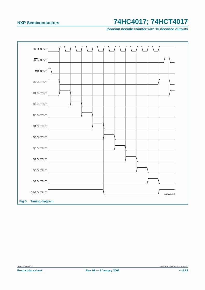
The 74HC4017; 74HCT4017 is a 5-stage Johnson decade counter with 10 decoded activeHIGH outputs (Q0 to Q9), an active LOW output from the most significant flip-flop (Q5-9),active HIGH and active LOW clock inputs (CP0 and CP1) and an overriding asynchronousmaster reset input (MR).
The counter is advanced by either a LOW-to-HIGH transition at CP0 while CP1 is LOW ora HIGH-to-LOW transition at CP1 while CP0 is HIGH (see Table 3).
When cascading counters, the Q5-9 output, which is LOW while the counter is in states 5,6, 7, 8 and 9, can be used to drive the CP0 input of the next counter.
A HIGH on MR resets the counter to zero (Q0 = Q5-9 = HIGH; Q1 to Q9 = LOW)independent of the clock inputs (CP0 and CP1).
Automatic code correction of the counter is provided by an internal circuit: following anyillegal code the counter returns to a proper counting mode within 11 clock pulses.
2. Features
Multiple package options
Complies with JEDEC standard no. 7 A
ESD protection:
HBM JESD22-A114E exceeds 2000 V
MM JESD22-A115-A exceeds 200 V
Specified from −40 °C to +85 °C and from −40 °C to +125 °C
74HC4017; 74HCT4017Johnson decade counter with 10 decoded outputsRev. 03 — 8 January 2008 Product data sheet

NXP Semiconductors 74HC4017; 74HCT4017Johnson decade counter with 10 decoded outputs
3. Ordering information
4. Functional diagram
Table 1. Ordering information
Type number Package
Temperature range Name Description Version
74HC4017
74HC4017N −40 °C to +125 °C DIP16 plastic dual in-line package; 16 leads (300 mil) SOT38-4
74HC4017D −40 °C to +125 °C SO16 plastic small outline package; 16 leads;body width 3.9 mm
SOT109-1
74HC4017DB −40 °C to +125 °C SSOP16 plastic shrink small outline package; 16 leads;body width 5.3 mm
SOT338-1
74HC4017PW −40 °C to +125 °C TSSOP16 plastic thin shrink small outline package; 16 leads;body width 4.4 mm
SOT403-1
74HC4017BQ −40 °C to +125 °C DHVQFN16 plastic dual in-line compatible thermal-enhancedvery thin quad flat package; no leads; 16 terminals;body 2.5 × 3.5 × 0.85 mm
SOT763-1
74HCT4017
74HCT4017N −40 °C to +125 °C DIP16 plastic dual in-line package; 16 leads (300 mil) SOT38-4
74HCT4017D −40 °C to +125 °C SO16 plastic small outline package; 16 leads;body width 3.9 mm
SOT109-1
74HCT4017BQ −40 °C to +125 °C DHVQFN16 plastic dual in-line compatible thermal-enhancedvery thin quad flat package; no leads; 16 terminals;body 2.5 × 3.5 × 0.85 mm
SOT763-1
Fig 1. Functional diagram
001aah242
DECODING AND OUTPUT CIRCUITRY
5-STAGE JOHNSON COUNTER
Q0
CP0
MR15
14
13CP1
3
Q1
2
Q2
4
Q3
7
Q4
10
Q5
1
Q6
5
Q7
6
Q8
9
Q9
Q5-9
11
12
74HC_HCT4017_3 © NXP B.V. 2008. All rights reserved.
Product data sheet Rev. 03 — 8 January 2008 2 of 23

NXP Semiconductors 74HC4017; 74HCT4017Johnson decade counter with 10 decoded outputs
Fig 2. Logic symbol Fig 3. IEC logic symbol
Q9
Q5-9
11
12
Q8 9
MR15
14
13CP0CP1
Q7 6
Q6
Q5 1
5
Q4
Q3 7
10
Q2 4
Q1 2
Q0 3
001aah239
9
CT≥5
11
12
89
CT = 0
CTRDIV10/DEC
15
13
14
76
6
51
5
4
37
10
24
12
03
001aah240
&
Fig 4. Logic diagram
001aah243
FF1
D
CP
RD
Q
Q
FF2
D
CP
RD
Q
Q
FF3
D
CP
RD
Q
Q
FF4
D
CP
RD
Q
Q
FF5
D
CP
RD
Q
Q
Q0
CP1
CP0
MR
Q1 Q2 Q3 Q4 Q5 Q6 Q7 Q8 Q9 Q5-9
74HC_HCT4017_3 © NXP B.V. 2008. All rights reserved.
Product data sheet Rev. 03 — 8 January 2008 3 of 23
NXP Semiconductors 74HC4017; 74HCT4017Johnson decade counter with 10 decoded outputs
Fig 5. Timing diagram
001aah244
CP0 INPUT
CP1 INPUT
MR INPUT
Q0 OUTPUT
Q1 OUTPUT
Q2 OUTPUT
Q3 OUTPUT
Q4 OUTPUT
Q5 OUTPUT
Q6 OUTPUT
Q7 OUTPUT
Q8 OUTPUT
Q9 OUTPUT
Q5-9 OUTPUT
74HC_HCT4017_3 © NXP B.V. 2008. All rights reserved.
Product data sheet Rev. 03 — 8 January 2008 4 of 23

NXP Semiconductors 74HC4017; 74HCT4017Johnson decade counter with 10 decoded outputs
5. Pinning information
5.1 Pinning
5.2 Pin description
Fig 6. Pin configuration DIP16, SO16 and (T)SSOP16 Fig 7. Pin configuration DHVQFN16
74HC401774HCT4017
Q5 VCC
Q1 MR
Q0 CP0
Q2 CP1
Q6 Q5-9
Q7 Q9
Q3 Q4
GND Q8
001aah238
1
2
3
4
5
6
7
8
10
9
12
11
14
13
16
15
001aah241
74HC401774HCT4017
Q3 Q4
Q7 Q9
Q6 Q5-9
Q2 CP1
Q0 CP0
Q1 MR
GN
D
Q8
Q5
VC
C
Transparent top view
7 10
6 11
5 12
4 13
3 14
2 15
8 9
1 16
terminal 1index area
GND(1)
Table 2. Pin description
Symbol Pin Description
Q[0:9] 3, 2, 4, 7, 10, 1, 5, 6, 9, 11 decoded output
GND 8 ground (0 V)
Q5-9 12 carry output (active LOW)
CP1 13 clock input (HIGH-to-LOW edge-triggered)
CP0 14 clock input (LOW-to-HIGH edge-triggered)
MR 15 master reset input (active HIGH)
VCC 16 supply voltage
74HC_HCT4017_3 © NXP B.V. 2008. All rights reserved.
Product data sheet Rev. 03 — 8 January 2008 5 of 23

NXP Semiconductors 74HC4017; 74HCT4017Johnson decade counter with 10 decoded outputs
6. Functional description
[1] H = HIGH voltage level;
L = LOW voltage level;
X = don’t care;
↑ = LOW-to-HIGH transition;
↓ = HIGH-to-LOW transition;
7. Limiting values
[1] The input and output voltage ratings may be exceeded if the input and output current ratings are observed.
[2] Ptot derates linearly with 12 mW/K above 70 °C.
[3] Ptot derates linearly with 8 mW/K above 70 °C.
[4] Ptot derates linearly with 5.5 mW/K above 60 °C.
[5] Ptot derates linearly with 4.5 mW/K above 60 °C.
Table 3. Function table [1]
MR CP0 CP1 Operation
H X X Q0 = Q5-9 = HIGH;Q1 to Q9 = LOW
L H ↓ counter advances
L ↑ L counter advances
L L X no change
L X H no change
L H ↑ no change
L ↓ L no change
Table 4. Limiting valuesIn accordance with the Absolute Maximum Rating System (IEC 60134). Voltages are referenced to GND (ground = 0 V).
Symbol Parameter Conditions Min Max Unit
VCC supply voltage −0.5 +7 V
IIK input clamping current VI < −0.5 V or VI > VCC + 0.5 V [1] - ±20 mA
IOK output clamping current VO < −0.5 V or VO > VCC + 0.5 V [1] - ±20 mA
IO output current −0.5 V < VO < VCC + 0.5 V - ±25 mA
ICC supply current - 50 mA
IGND ground current −50 - mA
Tstg storage temperature −65 +150 °C
Ptot total power dissipation Tamb = −40 °C to +125 °C
DIP16 package [2] - 750 mW
SO16 package [3] - 500 mW
(T)SSOP16 package [4] - 500 mW
DHVQFN16 package [5] - 500 mW
74HC_HCT4017_3 © NXP B.V. 2008. All rights reserved.
Product data sheet Rev. 03 — 8 January 2008 6 of 23

NXP Semiconductors 74HC4017; 74HCT4017Johnson decade counter with 10 decoded outputs
8. Recommended operating conditions
9. Static characteristics
Table 5. Recommended operating conditions
Symbol Parameter Conditions Min Typ Max Unit
74HC4017
VCC supply voltage 2.0 5.0 6.0 V
VI input voltage 0 - VCC V
VO output voltage 0 - VCC V
∆t/∆V input transition rise and fall rate VCC = 2.0 V - - 625 ns/V
VCC = 4.5 V - 1.67 139 ns/V
VCC = 6.0 V - - 83 ns/V
Tamb ambient temperature −40 - +125 °C
74HCT4017
VCC supply voltage 4.5 5.0 5.5 V
VI input voltage 0 - VCC V
VO output voltage 0 - VCC V
∆t/∆V input transition rise and fall rate VCC = 4.5 V - 1.67 139 ns/V
Tamb ambient temperature −40 - +125 °C
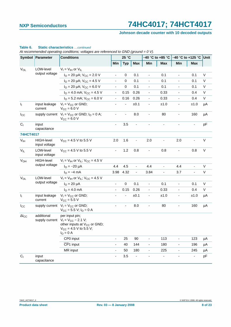
Table 6. Static characteristicsAt recommended operating conditions; voltages are referenced to GND (ground = 0 V).
Symbol Parameter Conditions 25 °C −40 °C to +85 °C −40 °C to +125 °C Unit
Min Typ Max Min Max Min Max
74HC4017
VIH HIGH-levelinput voltage
VCC = 2.0 V 1.5 1.2 - 1.5 - 1.5 - V
VCC = 4.5 V 3.15 2.4 - 3.15 - 3.15 - V
VCC = 6.0 V 4.2 3.2 - 4.2 - 4.2 - V
VIL LOW-levelinput voltage
VCC = 2.0 V - 0.8 0.5 - 0.5 - 0.5 V
VCC = 4.5 V - 2.1 1.35 - 1.35 - 1.35 V
VCC = 6.0 V - 2.8 1.8 - 1.8 - 1.8 V
VOH HIGH-leveloutput voltage
VI = VIH or VIL
IO = −20 µA; VCC = 2.0 V 1.9 2.0 - 1.9 - 1.9 - V
IO = −20 µA; VCC = 4.5 V 4.4 4.5 - 4.4 - 4.4 - V
IO = −20 µA; VCC = 6.0 V 5.9 6.0 - 5.9 - 5.9 - V
IO = −4.0 mA; VCC = 4.5 V 3.98 4.32 - 3.84 - 3.7 - V
IO = −5.2 mA; VCC = 6.0 V 5.48 5.81 - 5.34 - 5.2 - V
74HC_HCT4017_3 © NXP B.V. 2008. All rights reserved.
Product data sheet Rev. 03 — 8 January 2008 7 of 23
NXP Semiconductors 74HC4017; 74HCT4017Johnson decade counter with 10 decoded outputs
VOL LOW-leveloutput voltage
VI = VIH or VIL
IO = 20 µA; VCC = 2.0 V - 0 0.1 - 0.1 - 0.1 V
IO = 20 µA; VCC = 4.5 V - 0 0.1 - 0.1 - 0.1 V
IO = 20 µA; VCC = 6.0 V - 0 0.1 - 0.1 - 0.1 V
IO = 4.0 mA; VCC = 4.5 V - 0.15 0.26 - 0.33 - 0.4 V
IO = 5.2 mA; VCC = 6.0 V - 0.16 0.26 - 0.33 - 0.4 V
II input leakagecurrent
VI = VCC or GND;VCC = 6.0 V
- - ±0.1 - ±1.0 - ±1.0 µA
ICC supply current VI = VCC or GND; IO = 0 A;VCC = 6.0 V
- - 8.0 - 80 - 160 µA
CI inputcapacitance
- 3.5 - - - - - pF
74HCT4017
VIH HIGH-levelinput voltage
VCC = 4.5 V to 5.5 V 2.0 1.6 - 2.0 - 2.0 - V
VIL LOW-levelinput voltage
VCC = 4.5 V to 5.5 V - 1.2 0.8 - 0.8 - 0.8 V
VOH HIGH-leveloutput voltage
VI = VIH or VIL; VCC = 4.5 V
IO = −20 µA 4.4 4.5 - 4.4 - 4.4 - V
IO = −4 mA 3.98 4.32 - 3.84 - 3.7 - V
VOL LOW-leveloutput voltage
VI = VIH or VIL; VCC = 4.5 V
IO = 20 µA - 0 0.1 - 0.1 - 0.1 V
IO = 4.0 mA - 0.15 0.26 - 0.33 - 0.4 V
II input leakagecurrent
VI = VCC or GND;VCC = 5.5 V
- - ±0.1 - ±1.0 - ±1.0 µA
ICC supply current VI = VCC or GND;VCC = 5.5 V; IO = 0 A
- - 8.0 - 80 - 160 µA
∆ICC additionalsupply current
per input pin;VI = VCC − 2.1 V;other inputs at VCC or GND;VCC = 4.5 V to 5.5 V;IO = 0 A
CP0 input - 25 90 - 113 - 123 µA
CP1 input - 40 144 - 180 - 196 µA
MR input - 50 180 - 225 - 245 µA
CI inputcapacitance
- 3.5 - - - - - pF
Table 6. Static characteristics …continuedAt recommended operating conditions; voltages are referenced to GND (ground = 0 V).
Symbol Parameter Conditions 25 °C −40 °C to +85 °C −40 °C to +125 °C Unit
Min Typ Max Min Max Min Max
74HC_HCT4017_3 © NXP B.V. 2008. All rights reserved.
Product data sheet Rev. 03 — 8 January 2008 8 of 23

NXP Semiconductors 74HC4017; 74HCT4017Johnson decade counter with 10 decoded outputs
10. Dynamic characteristics
Table 7. Dynamic characteristicsGND = 0 V; tr = tf = 6 ns; CL = 50 pF; see Figure 11.
Symbol Parameter Conditions 25 °C −40 °C to +85 °C −40 °C to +125 °C Unit
Min Typ Max Min Max Min Max
74HC4017
tpd propagationdelay
CP0 to Qn; CP0 to Q5-9;see Figure 10
[1]
VCC = 2.0 V - 63 230 - 290 - 345 ns
VCC = 4.5 V - 23 46 - 58 - 69 ns
VCC = 5.0 V;CL = 15 pF
- 20 - - - - - ns
VCC = 6.0 V - 18 39 - 49 - 59 ns
CP1 to Qn; CP1 to Q5-9;see Figure 10
VCC = 2.0 V - 61 250 - 315 - 375 ns
VCC = 4.5 V - 22 50 - 63 - 75 ns
VCC = 5.0 V;CL = 15 pF
- 20 - - - - - ns
VCC = 6.0 V - 18 43 - 54 - 64 ns
tPHL HIGH to LOWpropagationdelay
MR to Q[1:9];see Figure 10
VCC = 2.0 V - 52 230 - 290 - 345 ns
VCC = 4.5 V - 19 46 - 58 - 69 ns
VCC = 6.0 V - 15 39 - 49 - 59 ns
tPLH LOW to HIGHpropagationdelay
MR to Q5-9, Q0;see Figure 10
VCC = 2.0 V - 55 230 - 290 - 345 ns
VCC = 4.5 V - 20 46 - 58 - 69 ns
VCC = 6.0 V - 16 39 - 49 - 59 ns
tt transition time see Figure 10 [2]
VCC = 2.0 V - 19 75 - 95 - 110 ns
VCC = 4.5 V - 7 15 - 19 - 22 ns
VCC = 6.0 V - 6 13 - 16 - 19 ns
tW pulse width CP0 and CP1 (HIGH orLOW); see Figure 9
VCC = 2.0 V 80 17 - 100 - 120 - ns
VCC = 4.5 V 16 6 - 20 - 24 - ns
VCC = 6.0 V 14 5 - 17 - 20 - ns
MR (HIGH); see Figure 9
VCC = 2.0 V 80 19 - 100 - 120 - ns
VCC = 4.5 V 16 7 - 20 - 24 - ns
VCC = 6.0 V 14 6 - 17 - 20 - ns
74HC_HCT4017_3 © NXP B.V. 2008. All rights reserved.
Product data sheet Rev. 03 — 8 January 2008 9 of 23

NXP Semiconductors 74HC4017; 74HCT4017Johnson decade counter with 10 decoded outputs
tsu set-up time CP1 to CP0; CP0 to CP1;see Figure 8
VCC = 2.0 V 50 −8 - 65 - 75 - ns
VCC = 4.5 V 10 −3 - 13 - 15 - ns
VCC = 6.0 V 9 −2 - 11 - 13 - ns
th hold time CP1 to CP0; CP0 to CP1;see Figure 8
VCC = 2.0 V 50 17 - 65 - 75 - ns
VCC = 4.5 V 10 6 - 13 - 15 - ns
VCC = 6.0 V 9 5 - 11 - 13 - ns
trec recovery time MR to CP0 andMR to CP1; see Figure 9
VCC = 2.0 V 5 −17 - 5 - 5 - ns
VCC = 4.5 V 5 −6 - 5 - 5 - ns
VCC = 6.0 V 5 −5 - 5 - 5 - ns
fmax maximumfrequency
CP0 or CP1; see Figure 9
VCC = 2.0 V 6.0 23 - 4.8 - 4.0 - MHz
VCC = 4.5 V 30 70 - 24 - 20 - MHz
VCC = 5.0 V;CL = 15 pF
- 77 - - - - - MHz
VCC = 6.0 V 25 83 - 28 - 24 - MHz
CPD powerdissipationcapacitance
VI = GND to VCC;VCC = 5 V; fi = 1 MHz
[3] - 35 - - - - - pF
74HCT4017
tpd propagationdelay
CP0 to Qn; CP0 to Q5-9;see Figure 10
[1]
VCC = 4.5 V - 25 46 - 58 - 69 ns
VCC = 5.0 V;CL = 15 pF
- 21 - - - - - ns
CP1 to Qn; CP1 to Q5-9;see Figure 10
VCC = 4.5 V - 25 50 - 63 - 75 ns
VCC = 5.0 V;CL = 15 pF
- 21 - - - - - ns
tPHL HIGH to LOWpropagationdelay
MR to Q[1:9];see Figure 10
VCC = 4.5 V - 22 46 - 58 - 69 ns
tPLH LOW to HIGHpropagationdelay
MR to Q5-9, Q0;see Figure 10
VCC = 4.5 V - 20 46 - 58 - 69 ns
Table 7. Dynamic characteristics …continuedGND = 0 V; tr = tf = 6 ns; CL = 50 pF; see Figure 11.
Symbol Parameter Conditions 25 °C −40 °C to +85 °C −40 °C to +125 °C Unit
Min Typ Max Min Max Min Max
74HC_HCT4017_3 © NXP B.V. 2008. All rights reserved.
Product data sheet Rev. 03 — 8 January 2008 10 of 23

NXP Semiconductors 74HC4017; 74HCT4017Johnson decade counter with 10 decoded outputs
[1] tpd is the same as tPHL and tPLH.
[2] tt is the same as tTHL and tTLH.
[3] CPD is used to determine the dynamic power dissipation (PD in µW):
PD = CPD × VCC2 × fi × N + ∑(CL × VCC
2 × fo) where:
fi = input frequency in MHz;
fo = output frequency in MHz;
CL = output load capacitance in pF;
VCC = supply voltage in V;
N = number of inputs switching;
∑(CL × VCC2 × fo) = sum of outputs.
tt transition time see Figure 10 [2]
VCC = 4.5 V - 7 15 - 19 - 22 ns
tW pulse width CP0 and CP1 (HIGH orLOW); see Figure 9
VCC = 4.5 V 16 7 - 20 - 24 - ns
MR (HIGH); see Figure 9
VCC = 4.5 V 16 4 - 20 - 24 - ns
tsu set-up time CP1 to CP0; CP0 to CP1;see Figure 8
VCC = 4.5 V 10 −3 - 13 - 15 - ns
th hold time CP1 to CP0; CP0 to CP1;see Figure 8
VCC = 4.5 V 10 6 - 13 - 15 - ns
trec recovery time MR to CP0 andMR to CP1; see Figure 9
VCC = 4.5 V 5 −5 - 5 - 5 - ns
fmax maximumfrequency
CP0 or CP1; see Figure 9
VCC = 4.5 V 30 61 - 24 - 20 - MHz
VCC = 5.0 V;CL = 15 pF
- 67 - - - - - MHz
CPD powerdissipationcapacitance
VI = GND to VCC − 1.5 V;VCC = 5 V; fi = 1 MHz
[3] - 36 - - - - - pF
Table 7. Dynamic characteristics …continuedGND = 0 V; tr = tf = 6 ns; CL = 50 pF; see Figure 11.
Symbol Parameter Conditions 25 °C −40 °C to +85 °C −40 °C to +125 °C Unit
Min Typ Max Min Max Min Max
74HC_HCT4017_3 © NXP B.V. 2008. All rights reserved.
Product data sheet Rev. 03 — 8 January 2008 11 of 23

NXP Semiconductors 74HC4017; 74HCT4017Johnson decade counter with 10 decoded outputs
11. Waveforms
Measurement points are given in Table 8.
VOL and VOH are typical voltage output levels that occur with the output load.
Fig 8. Waveforms showing the set-up and hold times for CP0 to CP1 and CP1 to CP0
thtsu
CP0 input
GND
GND
CP1 input
VM
VI
VI
thtsu
VM
001aah245
Measurement points are given in Table 8.
VOL and VOH are typical voltage output levels that occur with the output load.
Fig 9. Waveforms showing the minimum pulse width for CP0, CP1 and MR input; the maximum frequency forCP0 and CP1 input; the recovery time for MR and the MR input to Qn and Q5-9 output propagation delays
CP0 input
VI
GND
VI
GND
VI
GND
VOH
VOL
VOH
VOL
Q1 - Q9output
MR input
CP1 input
VM
VM
1/f max
tW
tWtrec
VM
1/f max
tW
tPLH
tPHL
VM
VM
001aah246
Q0, Q5 - Q9output
74HC_HCT4017_3 © NXP B.V. 2008. All rights reserved.
Product data sheet Rev. 03 — 8 January 2008 12 of 23

NXP Semiconductors 74HC4017; 74HCT4017Johnson decade counter with 10 decoded outputs
Measurement points are given in Table 8.
VOL and VOH are typical voltage output levels that occur with the output load.
Conditions: CP1 = LOW while CP0 is triggered on a LOW-to-HIGH transition and CP0 = HIGH, while CP1 is triggered on aHIGH-to-LOW transition.
Fig 10. Waveforms showing the propagation delays for CP0, CP1 to Qn, Q5-9 outputs and the output transitiontimes
CP0 input
VI
GND
VI
GND
VOH
VOL
VOH
VOL
Q1 - Q9output
CP1 input
VM
VM
tPLH
tPHL tPLH
tPHL
VM
tTLH tTHL
VM
001aah247
Q0, Q5 - Q9output
Table 8. Measurement points
Type Input Output
VM VM
74HC4017 0.5 × VCC 0.5 × VCC
74HCT4017 1.3 V 1.3 V
74HC_HCT4017_3 © NXP B.V. 2008. All rights reserved.
Product data sheet Rev. 03 — 8 January 2008 13 of 23

NXP Semiconductors 74HC4017; 74HCT4017Johnson decade counter with 10 decoded outputs
12. Application information
Some examples of applications for the 74HC4017; 74HCT4017 are:
• Decade counter with decimal decoding
• 1 out of n decoding counter (when cascaded)
• Sequential controller
• Timer
Figure 12 shows a technique for extending the number of decoded output states for the74HC4017; 74HCT4017. Decoded outputs are sequential within each stage and fromstage to stage, with no dead time (except propagation delay).
Test data is given in Table 9.
Definitions test circuit:
RT = Termination resistance should be equal to output impedance Zo of the pulse generator.
CL = Load capacitance including jig and probe capacitance.
RL = Load resistance.
S1 = Test selection switch.
Fig 11. Load circuitry for measuring switching times
VM VM
tW
tW
10 %
90 %
0 V
VI
VI
negativepulse
positivepulse
0 V
VM VM
90 %
10 %
tf
tr
tr
tf
001aad983
DUT
VCC VCC
VI VO
RT
RL S1
CL
openPULSEGENERATOR
Table 9. Test data
Type Input Load S1 position
VI tr, tf CL RL tPHL, tPLH tPZH, tPHZ tPZL, tPLZ
74HC4017 VCC 6 ns 15 pF, 50 pF 1 kΩ open GND VCC
74HCT4017 3 V 6 ns 15 pF, 50 pF 1 kΩ open GND VCC
74HC_HCT4017_3 © NXP B.V. 2008. All rights reserved.
Product data sheet Rev. 03 — 8 January 2008 14 of 23
NXP Semiconductors 74HC4017; 74HCT4017Johnson decade counter with 10 decoded outputs
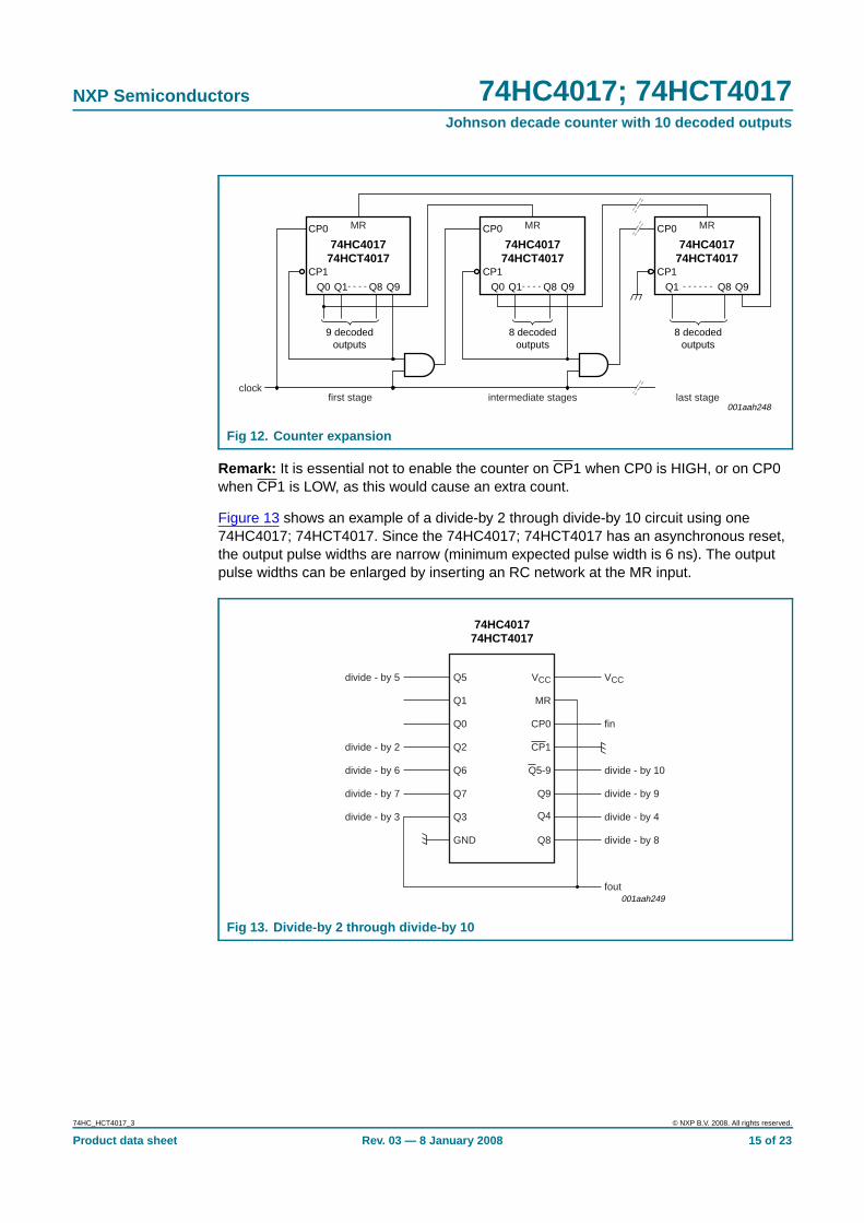
Remark: It is essential not to enable the counter on CP1 when CP0 is HIGH, or on CP0when CP1 is LOW, as this would cause an extra count.
Figure 13 shows an example of a divide-by 2 through divide-by 10 circuit using one74HC4017; 74HCT4017. Since the 74HC4017; 74HCT4017 has an asynchronous reset,the output pulse widths are narrow (minimum expected pulse width is 6 ns). The outputpulse widths can be enlarged by inserting an RC network at the MR input.
Fig 12. Counter expansion
Fig 13. Divide-by 2 through divide-by 10
001aah248
8 decodedoutputs
8 decodedoutputs
CP0
CP1
Q0 Q1 Q8 Q9
74HC401774HCT4017
74HC401774HCT4017
74HC401774HCT4017
- - - -
CP0
CP1
Q0 Q1 Q8 Q9- - - -
CP0
CP1
Q1 Q8 Q9- - - - - -
MR
clockfirst stage last stageintermediate stages
MR MR
9 decodedoutputs
Q4
Q8GND
divide - by 4
divide - by 8
Q9 divide - by 9
Q3divide - by 3
Q7divide - by 7
Q6divide - by 6
Q2divide - by 2
Q0
Q1
Q5divide - by 5
Q5-9 divide - by 10
CP1
CP0 fin
fout
MR
VCC VCC
001aah249
74HC401774HCT4017
74HC_HCT4017_3 © NXP B.V. 2008. All rights reserved.
Product data sheet Rev. 03 — 8 January 2008 15 of 23

NXP Semiconductors 74HC4017; 74HCT4017Johnson decade counter with 10 decoded outputs
13. Package outline
Fig 14. Package outline SOT38-4 (DIP16)
REFERENCESOUTLINEVERSION
EUROPEANPROJECTION ISSUE DATE
IEC JEDEC JEITA
SOT38-495-01-1403-02-13
MH
c
(e )1
ME
A
L
seat
ing
plan
e
A1
w Mb1
b2
e
D
A2
Z
16
1
9
8
E
pin 1 index
b
0 5 10 mm
scale
Note
1. Plastic or metal protrusions of 0.25 mm (0.01 inch) maximum per side are not included.
UNIT Amax.
1 2 b1(1) (1) (1)
b2 c D E e M ZHL
mm
DIMENSIONS (inch dimensions are derived from the original mm dimensions)
A min.
A max. b
max.wMEe1
1.731.30
0.530.38
0.360.23
19.5018.55
6.486.20
3.603.05
0.2542.54 7.628.257.80
10.08.3
0.764.2 0.51 3.2
inches 0.0680.051
0.0210.015
0.0140.009
1.250.85
0.0490.033
0.770.73
0.260.24
0.140.12
0.010.1 0.30.320.31
0.390.33
0.030.17 0.02 0.13
DIP16: plastic dual in-line package; 16 leads (300 mil) SOT38-4
74HC_HCT4017_3 © NXP B.V. 2008. All rights reserved.
Product data sheet Rev. 03 — 8 January 2008 16 of 23

NXP Semiconductors 74HC4017; 74HCT4017Johnson decade counter with 10 decoded outputs
Fig 15. Package outline SOT109-1 (SO16)
X
w M
θ
AA1
A2
bp
D
HE
Lp
Q
detail X
E
Z
e
c
L
v M A
(A )3
A
8
9
1
16
y
pin 1 index
UNITA
max. A1 A2 A3 bp c D (1) E(1) (1)e HE L L p Q Zywv θ
REFERENCESOUTLINEVERSION
EUROPEANPROJECTION ISSUE DATE
IEC JEDEC JEITA
mm
inches
1.750.250.10
1.451.25
0.250.490.36
0.250.19
10.09.8
4.03.8
1.276.25.8
0.70.6
0.70.3 8
0
o
o
0.25 0.1
DIMENSIONS (inch dimensions are derived from the original mm dimensions)
Note
1. Plastic or metal protrusions of 0.15 mm (0.006 inch) maximum per side are not included.
1.00.4
SOT109-199-12-2703-02-19
076E07 MS-012
0.0690.0100.004
0.0570.049
0.010.0190.014
0.01000.0075
0.390.38
0.160.15
0.05
1.05
0.0410.2440.228
0.0280.020
0.0280.012
0.01
0.25
0.01 0.0040.0390.016
0 2.5 5 mm
scale
SO16: plastic small outline package; 16 leads; body width 3.9 mm SOT109-1
74HC_HCT4017_3 © NXP B.V. 2008. All rights reserved.
Product data sheet Rev. 03 — 8 January 2008 17 of 23

NXP Semiconductors 74HC4017; 74HCT4017Johnson decade counter with 10 decoded outputs
Fig 16. Package outline SOT338-1 (SSOP16)
UNIT A1 A2 A3 bp c D (1) E (1) e HE L L p Q Zywv θ
REFERENCESOUTLINEVERSION
EUROPEANPROJECTION ISSUE DATE
IEC JEDEC JEITA
mm 0.210.05
1.801.65
0.250.380.25
0.200.09
6.46.0
5.45.2
0.65 1.257.97.6
1.030.63
0.90.7
1.000.55
80
o
o0.130.2 0.1
DIMENSIONS (mm are the original dimensions)
Note
1. Plastic or metal protrusions of 0.25 mm maximum per side are not included.
SOT338-199-12-2703-02-19
(1)
w Mbp
D
HE
E
Z
e
c
v M A
XA
y
1 8
16 9
θ
AA1
A2
Lp
Q
detail X
L
(A )3
MO-150
pin 1 index
0 2.5 5 mm
scale
SSOP16: plastic shrink small outline package; 16 leads; body width 5.3 mm SOT338-1
Amax.
2
74HC_HCT4017_3 © NXP B.V. 2008. All rights reserved.
Product data sheet Rev. 03 — 8 January 2008 18 of 23

NXP Semiconductors 74HC4017; 74HCT4017Johnson decade counter with 10 decoded outputs
Fig 17. Package outline SOT403-1 (TSSOP16)
UNIT A1 A2 A3 bp c D (1) E (2) (1)e HE L L p Q Zywv θ
REFERENCESOUTLINEVERSION
EUROPEANPROJECTION ISSUE DATE
IEC JEDEC JEITA
mm 0.150.05
0.950.80
0.300.19
0.20.1
5.14.9
4.54.3
0.656.66.2
0.40.3
0.400.06
80
o
o0.13 0.10.21
DIMENSIONS (mm are the original dimensions)
Notes
1. Plastic or metal protrusions of 0.15 mm maximum per side are not included.
2. Plastic interlead protrusions of 0.25 mm maximum per side are not included.
0.750.50
SOT403-1 MO-15399-12-2703-02-18
w Mbp
D
Z
e
0.25
1 8
16 9
θ
AA1
A2
Lp
Q
detail X
L
(A )3
HE
E
c
v M A
XA
y
0 2.5 5 mm
scale
TSSOP16: plastic thin shrink small outline package; 16 leads; body width 4.4 mm SOT403-1
Amax.
1.1
pin 1 index
74HC_HCT4017_3 © NXP B.V. 2008. All rights reserved.
Product data sheet Rev. 03 — 8 January 2008 19 of 23
NXP Semiconductors 74HC4017; 74HCT4017Johnson decade counter with 10 decoded outputs
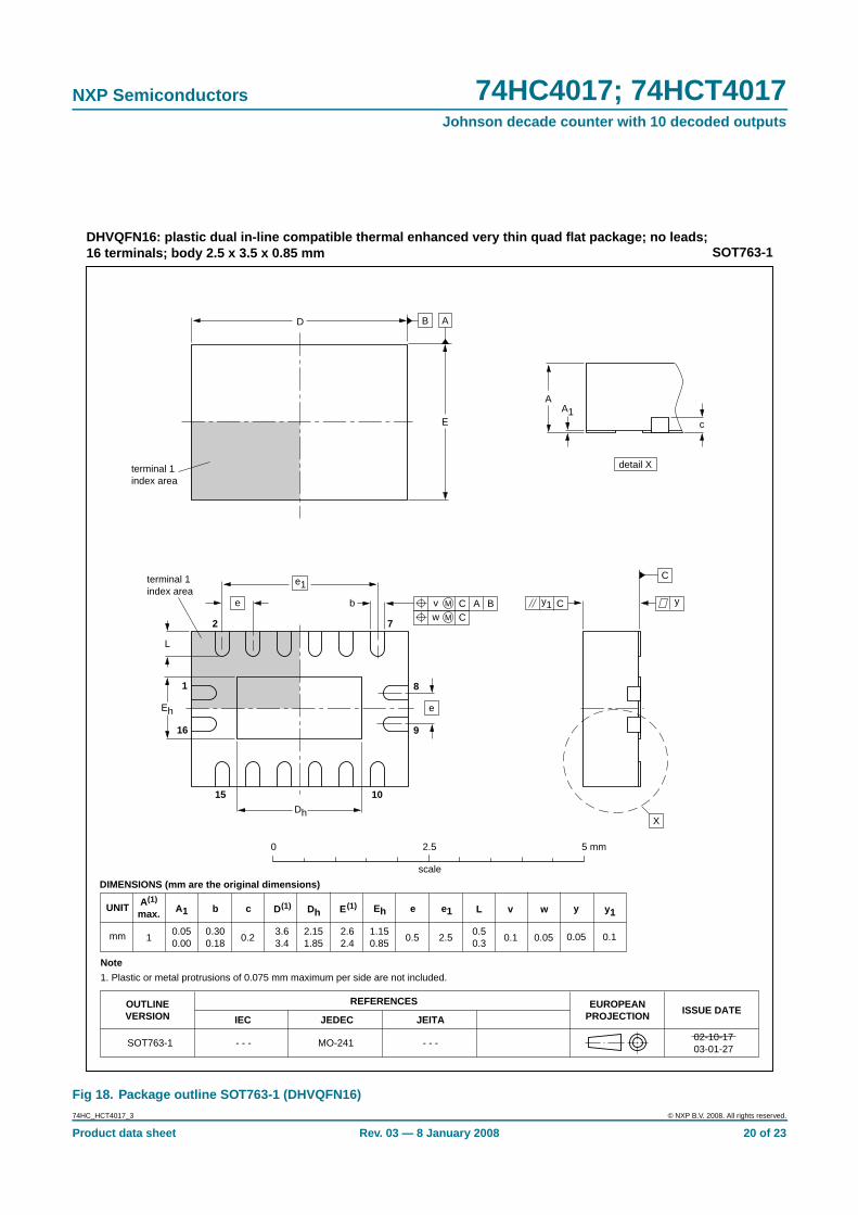
Fig 18. Package outline SOT763-1 (DHVQFN16)
terminal 1index area
0.51
A1 EhbUNIT ye
0.2
c
REFERENCESOUTLINEVERSION
EUROPEANPROJECTION ISSUE DATE
IEC JEDEC JEITA
mm 3.63.4
Dh
2.151.85
y1
2.62.4
1.150.85
e1
2.50.300.18
0.050.00
0.05 0.1
DIMENSIONS (mm are the original dimensions)
SOT763-1 MO-241 - - -- - -
0.50.3
L
0.1
v
0.05
w
0 2.5 5 mm
scale
SOT763-1DHVQFN16: plastic dual in-line compatible thermal enhanced very thin quad flat package; no leads;16 terminals; body 2.5 x 3.5 x 0.85 mm
A(1)
max.
AA1
c
detail X
yy1 Ce
L
Eh
Dh
e
e1
b
2 7
15 10
9
81
16
X
D
E
C
B A
terminal 1index area
ACC
Bv M
w M
E(1)
Note
1. Plastic or metal protrusions of 0.075 mm maximum per side are not included.
D(1)
02-10-1703-01-27
74HC_HCT4017_3 © NXP B.V. 2008. All rights reserved.
Product data sheet Rev. 03 — 8 January 2008 20 of 23

NXP Semiconductors 74HC4017; 74HCT4017Johnson decade counter with 10 decoded outputs
14. Abbreviations
15. Revision history
Table 10. Abbreviations
Acronym Description
CMOS Complementary Metal Oxide Semiconductor
DUT Device Under Test
ESD ElectroStatic Discharge
HBM Human Body Model
MM Machine Model
TTL Transistor-Transistor Logic
Table 11. Revision history
Document ID Release date Data sheet status Change notice Supersedes
74HC_HCT4017_3 20080108 Product data sheet - 74HC_HCT4017_CNV_2
Modifications: • The format of this data sheet has been redesigned to comply with the new identityguidelines of NXP Semiconductors.
• Legal texts have been adapted to the new company name where appropriate.
• Section 3: DHVQFN16 package added.
• Section 7: derating values added for DHVQFN16 package.
• Section 13: outline drawing added for DHVQFN16 package.
74HC_HCT4017_CNV_2 19970829 Product specification - -
74HC_HCT4017_3 © NXP B.V. 2008. All rights reserved.
Product data sheet Rev. 03 — 8 January 2008 21 of 23
NXP Semiconductors 74HC4017; 74HCT4017Johnson decade counter with 10 decoded outputs
16. Legal information
16.1 Data sheet status
[1] Please consult the most recently issued document before initiating or completing a design.
[2] The term ‘short data sheet’ is explained in section “Definitions”.
[3] The product status of device(s) described in this document may have changed since this document was published and may differ in case of multiple devices. The latest product statusinformation is available on the Internet at URL http://www.nxp.com.
16.2 Definitions
Draft — The document is a draft version only. The content is still underinternal review and subject to formal approval, which may result inmodifications or additions. NXP Semiconductors does not give anyrepresentations or warranties as to the accuracy or completeness ofinformation included herein and shall have no liability for the consequences ofuse of such information.
Short data sheet — A short data sheet is an extract from a full data sheetwith the same product type number(s) and title. A short data sheet is intendedfor quick reference only and should not be relied upon to contain detailed andfull information. For detailed and full information see the relevant full datasheet, which is available on request via the local NXP Semiconductors salesoffice. In case of any inconsistency or conflict with the short data sheet, thefull data sheet shall prevail.
16.3 Disclaimers
General — Information in this document is believed to be accurate andreliable. However, NXP Semiconductors does not give any representations orwarranties, expressed or implied, as to the accuracy or completeness of suchinformation and shall have no liability for the consequences of use of suchinformation.
Right to make changes — NXP Semiconductors reserves the right to makechanges to information published in this document, including withoutlimitation specifications and product descriptions, at any time and withoutnotice. This document supersedes and replaces all information supplied priorto the publication hereof.
Suitability for use — NXP Semiconductors products are not designed,authorized or warranted to be suitable for use in medical, military, aircraft,space or life support equipment, nor in applications where failure or
malfunction of an NXP Semiconductors product can reasonably be expectedto result in personal injury, death or severe property or environmentaldamage. NXP Semiconductors accepts no liability for inclusion and/or use ofNXP Semiconductors products in such equipment or applications andtherefore such inclusion and/or use is at the customer’s own risk.
Applications — Applications that are described herein for any of theseproducts are for illustrative purposes only. NXP Semiconductors makes norepresentation or warranty that such applications will be suitable for thespecified use without further testing or modification.
Limiting values — Stress above one or more limiting values (as defined inthe Absolute Maximum Ratings System of IEC 60134) may cause permanentdamage to the device. Limiting values are stress ratings only and operation ofthe device at these or any other conditions above those given in theCharacteristics sections of this document is not implied. Exposure to limitingvalues for extended periods may affect device reliability.
Terms and conditions of sale — NXP Semiconductors products are soldsubject to the general terms and conditions of commercial sale, as publishedat http://www.nxp.com/profile/terms, including those pertaining to warranty,intellectual property rights infringement and limitation of liability, unlessexplicitly otherwise agreed to in writing by NXP Semiconductors. In case ofany inconsistency or conflict between information in this document and suchterms and conditions, the latter will prevail.
No offer to sell or license — Nothing in this document may be interpretedor construed as an offer to sell products that is open for acceptance or thegrant, conveyance or implication of any license under any copyrights, patentsor other industrial or intellectual property rights.
16.4 TrademarksNotice: All referenced brands, product names, service names and trademarksare the property of their respective owners.
17. Contact information
For additional information, please visit: http://www .nxp.com
For sales office addresses, send an email to: salesad [email protected]
Document status [1] [2] Product status [3] Definition
Objective [short] data sheet Development This document contains data from the objective specification for product development.
Preliminary [short] data sheet Qualification This document contains data from the preliminary specification.
Product [short] data sheet Production This document contains the product specification.
74HC_HCT4017_3 © NXP B.V. 2008. All rights reserved.
Product data sheet Rev. 03 — 8 January 2008 22 of 23

NXP Semiconductors 74HC4017; 74HCT4017Johnson decade counter with 10 decoded outputs
18. Contents
1 General description . . . . . . . . . . . . . . . . . . . . . . 12 Features . . . . . . . . . . . . . . . . . . . . . . . . . . . . . . . 13 Ordering information . . . . . . . . . . . . . . . . . . . . . 24 Functional diagram . . . . . . . . . . . . . . . . . . . . . . 25 Pinning information . . . . . . . . . . . . . . . . . . . . . . 55.1 Pinning . . . . . . . . . . . . . . . . . . . . . . . . . . . . . . . 55.2 Pin description . . . . . . . . . . . . . . . . . . . . . . . . . 56 Functional description . . . . . . . . . . . . . . . . . . . 67 Limiting values. . . . . . . . . . . . . . . . . . . . . . . . . . 68 Recommended operating conditions. . . . . . . . 79 Static characteristics. . . . . . . . . . . . . . . . . . . . . 710 Dynamic characteristics . . . . . . . . . . . . . . . . . . 911 Waveforms . . . . . . . . . . . . . . . . . . . . . . . . . . . . 1212 Application information. . . . . . . . . . . . . . . . . . 1413 Package outline . . . . . . . . . . . . . . . . . . . . . . . . 1614 Abbreviations . . . . . . . . . . . . . . . . . . . . . . . . . . 2115 Revision history . . . . . . . . . . . . . . . . . . . . . . . . 2116 Legal information. . . . . . . . . . . . . . . . . . . . . . . 2216.1 Data sheet status . . . . . . . . . . . . . . . . . . . . . . 2216.2 Definitions . . . . . . . . . . . . . . . . . . . . . . . . . . . . 2216.3 Disclaimers . . . . . . . . . . . . . . . . . . . . . . . . . . . 2216.4 Trademarks . . . . . . . . . . . . . . . . . . . . . . . . . . . 2217 Contact information. . . . . . . . . . . . . . . . . . . . . 2218 Contents . . . . . . . . . . . . . . . . . . . . . . . . . . . . . . 23
© NXP B.V. 2008. All rights reserved.For more information, please visit: http://www.nxp.comFor sales office addresses, please send an email to: [email protected]
Date of release: 8 January 2008
Document identifier: 74HC_HCT4017_3
Please be aware that important notices concerning this document and the product(s)described herein, have been included in section ‘Legal information’.
Related Documents