2-1 Programming Interface PRELIMINARY Advancing the Standards 6x86 PROCESSOR Superscalar, Superpipelined, Sixth-generation, x86 Compatible CPU 2. PROGRAMMING INTERFACE In this chapter, the internal operations of the 6x86 CPU are described mainly from an appli- cation programmer’s point of view. Included in this chapter are descriptions of processor initial- ization, the register set, memory addressing, various types of interrupts and the shutdown and halt process. An overview of real, virtual 8086, and protected operating modes is also included in this chapter. The FPU operations are described separately at the end of the chap- ter. This manual does not—and is not intended to—describe the 6x86 microprocessor or its operations at the circuit level. 2.1 Processor Initialization The 6x86 CPU is initialized when the RESET signal is asserted. The processor is placed in real mode and the registers listed in Table 2-1 (Page 2-2) are set to their initialized values. RESET invalidates and disables the cache and turns off paging. When RESET is asserted, the 6x86 CPU terminates all local bus activity and all internal execution. During the entire time that RESET is asserted, the internal pipelines are flushed and no instruction execution or bus activity occurs. Approximately 150 to 250 external clock cycles after RESET is negated, the processor begins executing instructions at the top of physical memory (address location FFFF FFF0h). Typi- cally, an intersegment JUMP is placed at FFFF FFF0h. This instruction will force the processor to begin execution in the lowest 1 MByte of address space. Note: The actual time depends on the clock scaling in use. Also an additional 2 20 clock cycles are needed if self-test is requested.

Welcome message from author
This document is posted to help you gain knowledge. Please leave a comment to let me know what you think about it! Share it to your friends and learn new things together.
Transcript

2-1
Programming Interface
PRELIMINARY
Advancing the Standards
6x86 PROCESSORSuperscalar, Superpipelined,
Sixth-generation, x86 Compatible CPU
2. PROGRAMMINGINTERFACE
In this chapter, the internal operations of the 6x86 CPU are described mainly from an appli-cation programmer’s point of view. Included in this chapter are descriptions of processor initial-ization, the register set, memory addressing, various types of interrupts and the shutdown and halt process. An overview of real, virtual 8086, and protected operating modes is also included in this chapter. The FPU operations are described separately at the end of the chap-ter.
This manual does not—and is not intended to—describe the 6x86 microprocessor or its operations at the circuit level.
2.1 Processor Initialization
The 6x86 CPU is initialized when the RESET signal is asserted. The processor is placed in real mode and the registers listed in Table 2-1 (Page 2-2) are set to their initialized values. RESET invalidates and disables the cache and turns off paging. When RESET is asserted, the 6x86 CPU terminates all local bus activity and all internal execution. During the entire time that RESET is asserted, the internal pipelines are flushed and no instruction execution or bus activity occurs.
Approximately 150 to 250 external clock cyclesafter RESET is negated, the processor begins executing instructions at the top of physical memory (address location FFFF FFF0h). Typi-cally, an intersegment JUMP is placed at FFFF FFF0h. This instruction will force the processor to begin execution in the lowest 1 MByte of address space.
Note: The actual time depends on the clock scaling in use. Also an additional 220 clock cycles are needed if self-test is requested.

2-2 PRELIMINARY
Processor InitializationAdvancing the Standards
Table 2-1. Initialized Register Controls
REGISTER REGISTER NAME INITIALIZED CONTENTS COMMENTS
EAX Accumulator xxxx xxxxh 0000 0000h indicates self-test passed.
EBX Base xxxx xxxxh
ECX Count xxxx xxxxh
EDX Data 05 + Device ID Device ID = 31h or 33h (2X clock)Device ID = 35h or 37h (3X clock)
EBP Base Pointer xxxx xxxxh
ESI Source Index xxxx xxxxh
EDI Destination Index xxxx xxxxh
ESP Stack Pointer xxxx xxxxh
EFLAGS Flag Word 0000 0002h
EIP Instruction Pointer 0000 FFF0h
ES Extra Segment 0000h Base address set to 0000 0000h.Limit set to FFFFh.
CS Code Segment F000h Base address set to FFFF 0000h.Limit set to FFFFh.
SS Stack Segment 0000h Base address set to 0000 0000h.Limit set to FFFFh.
DS Data Segment 0000h Base address set to 0000 0000h.Limit set to FFFFh.
FS Extra Segment 0000h Base address set to 0000 0000h.Limit set to FFFFh.
GS Extra Segment 0000h Base address set to 0000 0000h.Limit set to FFFFh.
IDTR Interrupt Descriptor Table Register
Base = 0, Limit = 3FFh
GDTR Global Descriptor Table Register
xxxx xxxxh, xxxxh
LDTR Local Descriptor Table Register
xxxx xxxxh, xxxxh
TR Task Register xxxxh
CR0 Machine Status Word 6000 0010h
CR2 Control Register 2 xxxx xxxxh
CR3 Control Register 3 xxxx xxxxh
CCR (0-5) Configuration Control (0-5) 00h
ARR (0-7) Address Region Registers (0-7) 00h
RCR (0-7) Region Control Registers (0-7) 00h
DIR0 Device Identification 0 31h or 33h (2X clock)35h or 37h (3X clock)
DIR1 Device Identification 1 Step ID + Revision ID
DR7 Debug Register 7 0000 0400hNote: x = Undefined value

2-3
2
PRELIMINARY
Instruction Set Overview
2.2 Instruction SetOverview
The 6x86 CPU instruction set performs nine types of general operations:
All 6x86 CPU instructions operate on as few as zero operands and as many as three operands. An NOP instruction (no operation) is an exam-ple of a zero operand instruction. Two operand instructions allow the specification of an explicit source and destination pair as part of the instruction. These two operand instruc-tions can be divided into eight groups accord-ing to operand types:
An operand can be held in the instruction itself (as in the case of an immediate operand), in one of the processor’s registers or I/O ports, or in memory. An immediate operand is prefetched as part of the opcode for the instruction.
Operand lengths of 8, 16, or 32 bits are sup-ported as well as 64-or 80-bit associated with floating point instructions. Operand lengths of 8 or 32 bits are generally used when executing code written for 386- or 486-class (32-bit code) processors. Operand lengths of 8 or 16 bits are generally used when executing existing 8086 or 80286 code (16-bit code). The default length
• Arithmetic • High-Level Language Support
• Bit Manipulation • Operating System Support
• Control Transfer • Shift/Rotate
• Data Transfer • String Manipulation
• Floating Point
• Register to Register • Register to I/O
• Register to Memory • I/O to Register
• Memory to Register • Immediate Data to Register
• Memory to Memory • Immediate Data to Memory
of an operand can be overridden by placing one or more instruction prefixes in front of the opcode. For example, by using prefixes, a 32-bit operand can be used with 16-bit code, or a 16-bit operand can be used with 32-bit code.
Chapter 6 of this manual lists each instruction in the 6x86 CPU instruction set along with the associated opcodes, execution clock counts, and effects on the FLAGS register.
2.2.1 Lock Prefix
The LOCK prefix may be placed before certain instructions that read, modify, then write back to memory. The prefix asserts the LOCK# sig-nal to indicate to the external hardware that the CPU is in the process of running multiple indi-visible memory accesses. The LOCK prefix can be used with the following instructions:
Bit Test Instructions (BTS, BTR, BTC)Exchange Instructions (XADD, XCHG,
CMPXCHG)One-operand Arithmetic and Logical
Instructions (DEC, INC, NEG, NOT)Two-operand Arithmetic and Logical
Instructions (ADC, ADD, AND, OR, SBB, SUB, XOR).
An invalid opcode exception is generated if the LOCK prefix is used with any other instruction, or with the above instructions when no write operation to memory occurs (i.e., the destination is a register). The LOCK# signal can be negated to allow weak-locking for all of memory or on a regional basis. Refer to the descriptions of the NO-LOCK bit (within CCR1) and the WL bit (within RCRx) later in this chapter.
2-4 PRELIMINARY
Register SetsAdvancing the Standards
2.3 Register Sets
From the programmer’s point of view there are 58 accessible registers in the 6x86 CPU. These registers are grouped into two sets. The appli-cation register set contains the registers fre-quently used by application programmers, and the system register set contains the registers typically reserved for use by operating system programmers.
The application register set is made up of gen-eral purpose registers, segment registers, a flag register, and an instruction pointer register.
The system register set is made up of the remaining registers which include control reg-isters, system address registers, debug registers, configuration registers, and test registers.
Each of the registers is discussed in detail in the following sections.
2.3.1 ApplicationRegister Set
The application register set, (Figure 2-1, Page 2-5) consists of the registers most often used by the applications programmer. These registers are generally accessible and are not protected from read or write access.
The General Purpose Register contents are frequently modified by assembly language instructions and typically contain arithmetic and logical instruction operands.
Segment Registers in real mode contain the base address for each segment. In protected mode the segment registers contain segment selectors. The segment selectors provide index-ing for tables (located in memory) that contain the base address and limit for each segment, as well as access control information.
The Flag Register contains control bits used to reflect the status of previously executed instruc-tions. This register also contains control bits that affect the operation of some instructions.
The Instruction Pointer register points to the next instruction that the processor will execute. This register is automatically incremented by the processor as execution progresses.
2-5
2
PRELIMINARY
Register Sets
Figure 2-1. Application Register Set
EIP (Instruction Pointer)
CS (Code Segment Selector)
SS (Stack Segment Selector)
DS (Data Segment Selector)
ES (Extra Segment Selector)
FS (Extra Segment F Selector)
GS (Extra Segment G Selector)
EAX (Accumulator)
EBX (Base)
ECX (Count)
EDX (Data)
ESI (Source Index)
EDI (Destination Index)
EBP (Base Pointer)
ESP (Stack Pointer)
31 0
15 0
1531 16 0
IP
1700405
Segment Registers
General Purpose Registers
Instruction Pointer Register
EFLAGS (Flag Register) 1531 16 0
FLAGS
Flag Register
2.3.2 General PurposeRegisters
The general purpose registers are divided into four data registers, two pointer registers, and twoindex registers as shown in Figure 2-2 (Page 2-6).
The Data Registers are used by the applica-tions programmer to manipulate data struc-tures and to hold the results of logical and arithmetic operations. Different portions of the general data registers can be addressed by using different names.
An “E” prefix identifies the complete 32-bit register. An “X” suffix without the “E” prefix identifies the lower 16 bits of the register.
The lower two bytes of a data register can be addressed with an “H” suffix (identifies the upper byte) or an “L” suffix (identifies the lower byte). The _L and _H portions of a data regis-ters act as independent registers. For example, if the AH register is written to by an instruc-tion, the AL register bits remain unchanged.

2-6 PRELIMINARY
Register SetsAdvancing the Standards
Figure 2-2. General Purpose Registers
EAX (Accumulator)
EBX (Base)
ECX (Count)
EDX (Data)
ESI (Source Index)
EDI (Destination Index)
EBP (Base Pointer)
ESP (Stack Pointer)
AX
SI
DI
BP
SP
31 16 15 8 7 0
1746400
BX
CX
DX
AH
BH
CH
DH
AL
BL
CL
DL
The 6x86 CPU processor implements a stack using the ESP register. This stack is accessed during the PUSH and POP instructions, procedure calls, procedure returns, interrupts, exceptions, and interrupt/exception returns.
The microprocessor automatically adjusts the value of the ESP during operation of these instructions.The EBP register may be used to reference data passed on the stack during procedure calls. Local data may also be placed on the stack and referenced relative to BP. This register provides a mechanism to access stack data in high-level languages.
The Pointer and Index Registers are listed below.
SI or ESI Source IndexDI or EDI Destination IndexSP or ESP Stack PointerBP or EBP Base Pointer
These registers can be addressed as 16- or 32-bit registers, with the “E” prefix indicating 32 bits. The pointer and index registers can be used as general purpose registers, however, some instructions use a fixed assignment of these registers. For example, repeated string operations always use ESI as the source pointer, EDI as the destination pointer, and ECX as the counter. The instructions using fixed registers include multiply and divide, I/O access, string operations, translate, loop, variable shift and rotate, and stack operations.

2-7
2
PRELIMINARY
Register Sets
2.3.3 Segment Registers andSelectors
Segmentation provides a means of defining data structures inside the memory space of the microprocessor. There are three basic types of segments: code, data, and stack. Segments are used automatically by the processor to deter-mine the location in memory of code, data, and stack references.
There are six 16-bit segment registers:
CS Code SegmentDS Data SegmentES Extra SegmentSS Stack SegmentFS Additional Data SegmentGS Additional Data Segment.
In real and virtual 8086 operating modes, a seg-ment register holds a 16-bit segment base. The 16-bit segment is multiplied by 16 and a 16-bit or 32-bit offset is then added to it to create a lin-ear address. The offset size is dependent on the current address size. In real mode and in vir-
tual 8086 mode with paging disabled, the linear address is also the physical address. In virtual 8086 mode with paging enabled, the linear address is translated to the physical address using the current page tables. Paging is described in Section 2.6.4 (Page 2-45).
In protected mode a segment register holds a Segment Selector containing a 13-bit index, a Table Indicator (TI) bit, and a two-bit Requested Privilege Level (RPL) field as shown in Figure 2-3.
The Index points into a descriptor table in memory and selects one of 8192 (213) segment descriptors contained in the descriptor table.
A segment descriptor is an eight-byte value used to describe a memory segment by defining the segment base, the segment limit, and access control information. To address data within a segment, a 16-bit or 32-bit offset is added to the segment’s base address. Once a segment selec-tor has been loaded into a segment register, an instruction needs only to specify the segment register and the offset.
Figure 2-3. Segment Selector in Protected Mode
INDEX RPL
1741701
15 3 2 1 0
TI
Descriptor
Descriptor Table
Segment
Main Memory
Segment Selector
Base
Limit
0
8191

2-8 PRELIMINARY
Register SetsAdvancing the Standards
The Table Indicator (TI) bit of the selector defines which descriptor table the index points into. If TI=0, the index references the Global Descriptor Table (GDT). If TI=1, the index ref-erences the Local Descriptor Table (LDT). The GDT and LDT are described in more detail in Section 2.4.2. Protected mode addressing is dis-cussed further in Sections 2.6.2 and 2.6.3.
The Requested Privilege Level (RPL) field in a segment selector is used to determine the Effec-tive Privilege Level of an instruction (where RPL=0 indicates the most privileged level, and RPL=3 indicates the least privileged level).
If the level requested by RPL is less than the Current Program Level (CPL), the RPL level is accepted and the Effective Privilege Level is changed to the RPL value. If the level requested by RPL is greater than CPL, the CPL overrides the requested RPL and Effective Privilege Level remains unchanged.
When a segment register is loaded with a seg-ment selector, the segment base, segment limit and access rights are loaded from the descriptor table entry into a user-invisible or hidden por-tion of the segment register (i.e., cached on-chip). The CPU does not access the descrip-tor table entry again until another segment reg-ister load occurs. If the descriptor tables are modified in memory, the segment registers must be reloaded with the new selector values by the software.
The processor automatically selects an implied (default) segment register for memory refer-ences. Table 2-2 describes the selection rules. In general, data references use the selector con-tained in the DS register, stack references use the SS register and instruction fetches use the CS register. While some of these selections may be overridden, instruction fetches, stack opera-tions, and the destination write of string opera-tions cannot be overridden. Special segment override instruction prefixes allow the use of alternate segment registers including the use of the ES, FS, and GS segment registers.
Table 2-2. Segment Register Selection Rules
TYPE OF MEMORY REFERENCEIMPLIED (DEFAULT)
SEGMENTSEGMENT OVERRIDE
PREFIX
Code Fetch CS None
Destination of PUSH, PUSHF, INT, CALL, PUSHA instructions
SS None
Source of POP, POPA, POPF, IRET, RET instructions
SS None
Destination of STOS, MOVS, REP STOS, REP MOVS instructions
ES None
Other data references with effective address using base registers of: EAX, EBX, ECX, EDX, ESI, EDI EBP, ESP
DS
SS
CS, ES, FS, GS, SS
CS, DS, ES, FS, GS

2-9
2
PRELIMINARY
Register Sets
2.3.4 Instruction PointerRegister
The Instruction Pointer (EIP) register contains the offset into the current code segment of the next instruction to be executed. The register is nor-mally incremented with each instruction execu-tion unless implicitly modified through an interrupt, exception or an instruction that changes the sequential execution flow (e.g., JMP, CALL).
2.3.5 Flags Register
The Flags Register, EFLAGS, contains status information and controls certain operations on the 6x86 CPU microprocessor. The lower 16 bits of this register are referred to as the FLAGS register that is used when executing 8086 or 80286 code. The flag bits are shown in Figure 2-4 and defined in Table 2-3 (Page 2-10).
Figure 2-4. EFLAGS Register
Flags
Alignment Check
1701105
Virtual 8086 ModeResume FlagNested Task FlagI/O Privilege LevelOverflowDirection FlagInterrupt EnableTrap FlagSign FlagZero FlagAuxiliary CarryParity FlagCarry Flag
0 0 0 0 0 0 0 0 0 0 0 0
0 or 1 Indicates ReservedA = Arithmetic Flag, D = Debug Flag, S = System Flag, C = Control Flag
9 8 7 6 5 4 3 1 2 0C
1P
0A
0ZSTIDOION
0RVA
31
24
23
19
1 1 1 1 1 1 1 1 18 7 6 5 4 3 2 1 0
C M F T PL F F F F F F F F F
SSDSSACSDAA
AAA
Identification S
21ID

2-10 PRELIMINARY
Register SetsAdvancing the Standards
Table 2-3. EFLAGS Bit Definitions
BITPOSITION
NAME FUNCTION
0 CF Carry Flag: Set when a carry out of (addition) or borrow into (subtraction) the mostsignificant bit of the result occurs; cleared otherwise.
2 PF Parity Flag: Set when the low-order 8 bits of the result contain an even number of ones;cleared otherwise.
4 AF Auxiliary Carry Flag: Set when a carry out of (addition) or borrow into (subtraction) bit position 3 of the result occurs; cleared otherwise.
6 ZF Zero Flag: Set if result is zero; cleared otherwise.
7 SF Sign Flag: Set equal to high-order bit of result (0 indicates positive, 1 indicates negative).
8 TF Trap Enable Flag: Once set, a single-step interrupt occurs after the next instructioncompletes execution. TF is cleared by the single-step interrupt.
9 IF Interrupt Enable Flag: When set, maskable interrupts (INTR input pin) are acknowledged and serviced by the CPU.
10 DF Direction Flag: If DF=0, string instructions auto-increment (default) the appropriate index registers (ESI and/or EDI). If DF=1, string instructions auto-decrement the appropriate index registers.
11 OF Overflow Flag: Set if the operation resulted in a carry or borrow into the sign bit of the result but did not result in a carry or borrow out of the high-order bit. Also set if theoperation resulted in a carry or borrow out of the high-order bit but did not result in a carry or borrow into the sign bit of the result.
12, 13 IOPL I/O Privilege Level: While executing in protected mode, IOPL indicates the maximumcurrent privilege level (CPL) permitted to execute I/O instructions without generating an exception 13 fault or consulting the I/O permission bit map. IOPL also indicates themaximum CPL allowing alteration of the IF bit when new values are popped into the EFLAGS register.
14 NT Nested Task: While executing in protected mode, NT indicates that the execution of the current task is nested within another task.
16 RF Resume Flag: Used in conjunction with debug register breakpoints. RF is checked at instruction boundaries before breakpoint exception processing. If set, any debug fault is ignored on the next instruction.
17 VM Virtual 8086 Mode: If set while in protected mode, the microprocessor switches to virtual 8086 operation handling segment loads as the 8086 does, but generating exception 13 faults on privileged opcodes. The VM bit can be set by the IRET instruction (if current privilege level=0) or by task switches at any privilege level.
18 AC Alignment Check Enable: In conjunction with the AM flag in CR0, the AC flag determines whether or not misaligned accesses to memory cause a fault. If AC is set, alignment faults are enabled.
21 ID Identification Bit: The ability to set and clear this bit indicates that the CPUID instruction is supported. The ID can be modified only if the CPUID bit in CCR4 is set.

2-11
2
PRELIMINARY
System Register Set
2.4 System Register Set
The system register set, shown in Figure 2-5 (Page 2-12), consists of registers not generally used by application programmers. These regis-ters are typically employed by system level pro-grammers who generate operating systems and memory management programs.
The Control Registers control certain aspects of the 6x86 microprocessor such as paging, coprocessor functions, and segment protection. When a paging exception occurs while paging is enabled, some control registers retain the lin-ear address of the access that caused the excep-tion.
The Descriptor Table Registers and the Task Register can also be referred to as system address or memory management registers. These registers consist of two 48-bit and two 16-bit registers. These registers specify the location of the data structures that control the segmentation used by the 6x86 microproces-sor. Segmentation is one available method of memory management.
The Configuration Registers are used to con-figure the 6x86 CPU on-chip cache operation, power management features and System Man-agement Mode. The configuration registers also provide information on the CPU device type and revision.
The Debug Registers provide debugging facil-ities to enable the use of data access break-points and code execution breakpoints.
The Test Registers provide a mechanism to test the contents of both the on-chip 16 KByte cache and the Translation Lookaside Buffer (TLB). In the following sections, the system register set is described in greater detail.

2-12 PRELIMINARY
System Register SetAdvancing the Standards
Figure 2-5. System Register Set
Control
Test
DR0DR1DR2DR3DR6DR7
GDTRIDTRLDTR
TR
CR0CR2CR3
1531 16 0
1516 0
Page Fault Linear Address RegisterPage Directory Base Register
47
31 0 Linear Breakpoint Address 0
Breakpoint StatusBreakpoint Control
Cache Test
CCR1CCR2
0
31 0
TLB Test ControlTLB Test Status
Cache Test Cache Test
Linear Breakpoint Address 1Linear Breakpoint Address 2Linear Breakpoint Address 3
7CCR0CCR1
BaseBase
LimitLimit
SelectorSelector Task Register
Descriptor
1728200
Registers
TableRegisters
CCR2
Address Region Register 0
CCR3
ARR0
Registers
DIR0DIR1
DIR0DIR1
CCR3
23
CCR0
CCR4CCR4CCR5CCR5
Address Region Register 1 ARR1
Address Region Register 2 ARR2
Address Region Register 3 ARR3
Address Region Register 4 ARR4
Address Region Register 5 ARR5
Address Region Register 6 ARR6
Address Region Register 7 ARR7
RCR0
RCR1
RCR2
RCR3
RCR4
RCR5
RCR6
RCR7
07
ConfigurationRegisters
CCR = Configuration Control Register
RCR = Region Control Register
DIR = Device Identification Register
DebugRegisters
TR3TR4TR5TR6TR7

2-13
2
PRELIMINARY
System Register Set
2.4.1 Control Registers
The Control Registers (CR0, CR2 and CR3), are shown in Figure 2-6. The CR0 register containssystem control bits which configure operating modes and indicate the general state of the CPU. The lower 16 bits of CR0 are referred to as the Machine Status Word (MSW). The CR0 bit def-initions are described in Table 2-4 and Table 2-5 (Page 2-14). The reserved bits in CR0 should not be modified.
When paging is enabled and a page fault is gen-erated, the CR2 register retains the 32-bit linear address of the address that caused the fault. When a double page fault occurs, CR2 contains the address for the second fault. Register CR3
contains the 20 most significant bits of the phys-ical base address of the page directory. The page directory must always be aligned to a 4-KByte page boundary, therefore, the lower 12 bits of CR3 are not required to specify the base address.
CR3 contains the Page Cache Disable (PCD) and Page Write Through (PWT) bits. During bus cycles that are not paged, the state of the PCD bit is reflected on the PCD pin and the PWT bit is driven on the PWT pin. These bus cycles include interrupt acknowledge cycles and all bus cycles, when paging is not enabled. The PCD pin should be used to control caching in an external cache. The PWT pin should be used to control write policy in an external cache.
Figure 2-6. Control Registers
PAGE FAULT LINEAR ADDRESS
CR3
CR2
CR0
1700703MSW
PAGE DIRECTORY BASE REGISTER (PDBR) RESV.RESERVED
31 12 11 4 3 0
P P
1RESERVED RESERVEDT E M PA WP C N
WT
CD
S M P EM P
01234161831 30 29
G D WNE
5
2-14 PRELIMINARY
System Register SetAdvancing the Standards
Table 2-4. CR0 Bit Definitions
BITPOSITION
NAME FUNCTION
0 PE Protected Mode Enable: Enables the segment based protection mechanism. If PE=1, protected mode is enabled. If PE=0, the CPU operates in real mode and addresses are formed as in an 8086-style CPU.
1 MP Monitor Processor Extension: If MP=1 and TS=1, a WAIT instruction causes Device Not Avail-able (DNA) fault 7. The TS bit is set to 1 on task switches by the CPU. Floating point instruc-tions are not affected by the state of the MP bit. The MP bit should be set to one during normal operations.
2 EM Emulate Processor Extension: If EM=1, all floating point instructions cause a DNA fault 7.
3 TS Task Switched: Set whenever a task switch operation is performed. Execution of a floating point instruction with TS=1 causes a DNA fault. If MP=1 and TS=1, a WAIT instruction also causes a DNA fault.
4 1 Reserved: Do not attempt to modify.
5 NE Numerics Exception. NE=1 to allow FPU exceptions to be handled by interrupt 16. NE=0 ifFPU exceptions are to be handled by external interrupts.
16 WP Write Protect: Protects read-only pages from supervisor write access. WP=0 allows a read-only page to be written from privilege level 0-2. WP=1 forces a fault on a write to aread-only page from any privilege level.
18 AM Alignment Check Mask: If AM=1, the AC bit in the EFLAGS register is unmasked and allowed to enable alignment check faults. Setting AM=0 prevents AC faults from occurring.
29 NW Not Write-Back: If NW=1, the on-chip cache operates in write-through mode. In write-through mode, all writes (including cache hits) are issued to the external bus. If NW=0, the on-chip cache operates in write-back mode. In write-back mode, writes are issued to the external bus only for a cache miss, a line replacement of a modified line, or as the result of a cache inquiry cycle.
30 CD Cache Disable: If CD=1, no further cache line fills occur. However, data already present in the cache continues to be used if the requested address hits in the cache. Writes continue to update the cache and cache invalidations due to inquiry cycles occur normally. The cache must also be invalidated to completely disable any cache activity.
31 PG Paging Enable Bit: If PG=1 and protected mode is enabled (PE=1), paging is enabled. After changing the state of PG, software must execute an unconditional branch instruction (e.g., JMP, CALL) to have the change take effect.
Table 2-5. Effects of Various Combinations of EM, TS, and MP Bits
CR0 BIT INSTRUCTION TYPEEM TS MP WAIT ESC
0 0 0 Execute Execute
0 0 1 Execute Execute
0 1 0 Execute Fault 7
0 1 1 Fault 7 Fault 7
1 0 0 Execute Fault 7
1 0 1 Execute Fault 7
1 1 0 Execute Fault 7
1 1 1 Fault 7 Fault 7

2-15
2
PRELIMINARY
System Register Set
2.4.2 Descriptor TableRegisters and Descriptors
Descriptor Table Registers
The Global, Interrupt, and Local Descriptor Table Registers (GDTR, IDTR and LDTR), shownin Figure 2-7, are used to specify the location of the data structures that control segmented memory management. The GDTR, IDTR and LDTR are loaded using the LGDT, LIDT and LLDT instructions, respectively. The values of these registers are stored using the correspond-ing store instructions. The GDTR and IDTR load instructions are privileged instructions when operating in protected mode. The LDTR can only be accessed in protected mode.
The Global Descriptor Table Register (GDTR)holds a 32-bit linear base address and 16-bit limit for the Global Descriptor Table (GDT). The GDT is an array of up to 8192 8-byte descriptors. When a segment register is loaded from memory, the TI bit in the segment selector chooses either the GDT or the Local Descriptor Table (LDT) to locate a descriptor. If TI = 0, the index portion of the selector is used to locate the descriptor within the GDT table. The contents of the GDTR are completely visible to the pro-
grammer by using a SGDT instruction. The first descriptor in the GDT (location 0) is not used by the CPU and is referred to as the “null descrip-tor”. The GDTR is initialized using a LGDT instruction.
The Interrupt Descriptor Table Register(IDTR) holds a 32-bit linear base address and 16-bit limit for the Interrupt Descriptor Table (IDT). The IDT is an array of 256 interrupt descriptors, each of which is used to point to an interrupt service routine. Every interrupt that may occur in the system must have an associ-ated entry in the IDT. The contents of the IDTR are completely visible to the programmer by using a SIDT instruction. The IDTR is initialized using the LIDT instruction.
The Local Descriptor Table Register (LDTR)holds a 16-bit selector for the Local Descriptor Table (LDT). The LDT is an array of up to 8192 8-byte descriptors. When the LDTR is loaded, the LDTR selector indexes an LDT descriptor that must reside in the Global Descriptor Table (GDT). The base address and limit are loaded automatically and cached from the LDT descrip-tor within the GDT.
Figure 2-7. Descriptor Table Registers
1708003
BASE ADDRESS LIMIT
SELECTOR
47 16 15 0
LDTR
IDTR
GDTRBASE ADDRESS LIMIT
2-16 PRELIMINARY
System Register SetAdvancing the Standards
Subsequent access to entries in the LDT use the hidden LDTR cache to obtain linear addresses. If the LDT descriptor is modified in the GDT, the LDTR must be reloaded to update the hidden portion of the LDTR.
When a segment register is loaded from mem-ory, the TI bit in the segment selector chooses either the GDT or the LDT to locate a segment descriptor. If TI = 1, the index portion of the selector is used to locate a given descriptor within the LDT. Each task in the system may be given its own LDT, managed by the operating system. The LDTs provide a method of isolating a given task’s segments from other tasks in the system.
The LDTR can be read or written by the LLDT and SLDT instructions.
Descriptors
There are three types of descriptors:
• Application Segment Descriptors that define code, data and stack segments.
• System Segment Descriptors that define an LDT segment or a Task State Segment (TSS) table described later in this text.
• Gate Descriptors that define task gates, interrupt gates, trap gates and call gates.
Application Segment Descriptors can be located in either the LDT or GDT. System Segment Descriptors can only be located in the GDT. Dependent on the gate type, gate descriptors may be located in either the GDT, LDT or IDT. Figure 2-8 illustrates the descriptor format for both Application Segment Descriptors and Sys-tem Segment Descriptors. Table 2-6 (Page 2-17) lists the corresponding bit definitions.
Figure 2-8. Application and System Segment Descriptors
BASE 15-0
31
P DPL D TYPE
+0
+4
1707803
2324 16
G D 0A
LIMIT 19-16 BASE 23-16
LIMIT 15-0
15 14 13 12 11 8 7 022 21 20 19
VL TBASE 31-24

2-17
2
PRELIMINARY
System Register Set
Table 2-6. Segment Descriptor Bit Definitions
BITPOSITION
MEMORYOFFSET
NAME DESCRIPTION
31-247-0
31-16
+4+4+0
BASE Segment base address.32-bit linear address that points to the beginning of the segment.
19-1615-0
+4+0
LIMIT Segment limit.
23 +4 G Limit granularity bit:0 = byte granularity, 1 = 4 KBytes (page) granularity.
22 +4 D Default length for operands and effective addresses.Valid for code and stack segments only: 0 = 16 bit, 1 = 32-bit.
20 +4 AVL Segment available.
15 +4 P Segment present.
14-13 +4 DPL Descriptor privilege level.
12 +4 DT Descriptor type:0 = system, 1 = application.
11-8 +4 TYPE Segment type. See Tables 2-7 and 2-8.
Table 2-7. TYPE Field Definitions with DT = 0
TYPE(BITS 11-8)
DESCRIPTION
0001 TSS-16 descriptor, task not busy.
0010 LDT descriptor.
0011 TSS-16 descriptor, task busy.
1001 TSS-32 descriptor, task not busy
1011 TSS-32 descriptor, task busy.
2-18 PRELIMINARY
System Register SetAdvancing the Standards
Table 2-8. TYPE Field Definitions with DT = 1
TYPEAPPLICATION DECRIPTOR INFORMATION
E C/D R/W A
0 0 x x data, expand up, limit is upper bound of segment
0 1 x x data, expand down, limit is lower bound of segment
1 0 x x executable, non-conforming
1 1 x x executable, conforming (runs at privilege level of calling procedure)
0 x 0 x data, non-writable
0 x 1 x data, writable
1 x 0 x executable, non-readable
1 x 1 x executable, readable
x x x 0 not-accessed
x x x 1 accessed
2-19
2
PRELIMINARY
System Register Set
System Register Set
Interrupt Gate Descriptors are used to enter a hardware interrupt service routine. Trap Gate Descriptors are used to enter exceptions or soft-ware interrupt service routines. Trap Gate and Interrupt Gate Descriptors can only be located in the IDT.
Call Gate Descriptors are used to enter a proce-dure (subroutine) that executes at the same or a more privileged level. A Call Gate Descriptor primarily defines the procedure entry point and the procedure’s privilege level.
Figure 2-9. Gate Descriptor
Table 2-9. Gate Descriptor Bit Definitions
BITPOSITION
MEMORYOFFSET
NAME DESCRIPTION
31-1615-0
+4+0
OFFSET Offset used during a call gate to calculate the branch target.
31-16 +0 SELECTOR Segment selector used during a call gate to calculate the branch target.
15 +4 P Segment present.
14-13 +4 DPL Descriptor privilege level.
11-8 +4 TYPE Segment type:0100 = 16-bit call gate0101 = task gate0110 = 16-bit interrupt gate0111 = 16-bit trap gate1100 = 32-bit call gate1110 = 32-bit interrupt gate1111 = 32-bit trap gate.
4-0 +4 PARAMETERS Number of 32-bit parameters to copy from the caller’s stack to the called procedure’s stack (valid for calls).
OFFSET 31-16
SELECTOR 15-0
31
P TYPE0 PARAMETERS
+0
+4
1707903
16
0
OFFSET 15-0
15 14 13 12 11 8 7 0
0 0DPL
Gate Descriptors provide protection for exe-cutable segments operating at different privilege levels. Figure 2-9 illustrates the format for Gate Descriptors and Table 2-9 lists the corresponding bit definitions.
Task Gate Descriptors are used to switch the CPU’s context during a task switch. The selec-tor portion of the task gate descriptor locates a Task State Segment. These descriptors can be located in the GDT, LDT or IDT tables.
2-20 PRELIMINARY
System Register SetAdvancing the Standards
2.4.3 Task Register
The Task Register (TR) holds a 16-bit selector for the current Task State Segment (TSS) table as shown in Figure 2-10. The TR is loaded and stored via the LTR and STR instructions, respec-tively. The TR can only be accessed during pro-tected mode and can only be loaded when the privilege level is 0 (most privileged). When the TR is loaded, the TR selector field indexes a TSS descriptor that must reside in the Global
Descriptor Table (GDT). The contents of the selected descriptor are cached on-chip in the hid-den portion of the TR.
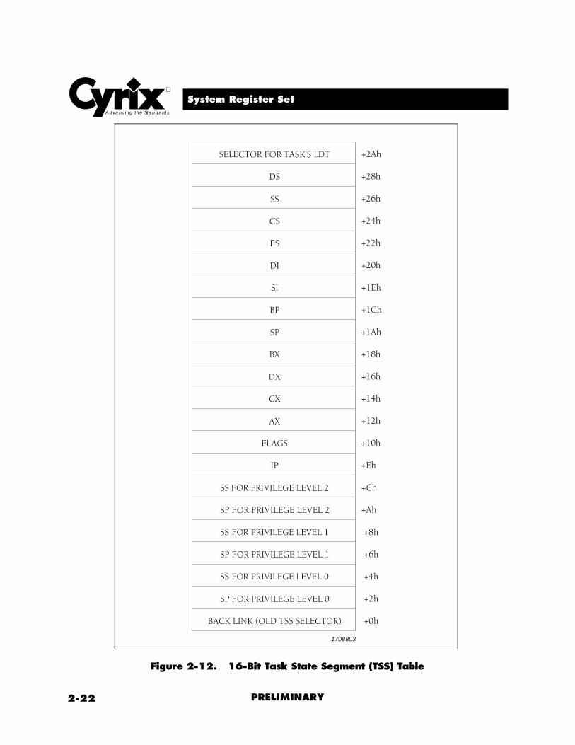
During task switching, the processor saves the cur-rent CPU state in the TSS before starting a new task. The TR points to the current TSS. The TSS can be either a 386/486-style 32-bit TSS(Figure 2-11, Page 2-21) or a 286-style 16-bit TSS type (Figure 2-12, Page 2-22). An I/O permission bit map is referenced in the 32-bit TSS by the I/O Map Base Address.
Figure 2-10. Task Register
1708103
SELECTOR
15 0

2-21
2
PRELIMINARY
System Register Set
Figure 2-11. 32-Bit Task State Segment (TSS) Table
+0h+4h+8h+Ch+10h+14h+18h+1Ch+20h+24h+28h+2Ch+30h+34h
BACK LINK (OLD TSS SELECTOR)
SS for CPL = 0
SS for CPL = 1
SS for CPL = 2
+38h+3Ch+40h+44h+48h+4Ch+50h+54h+58h+5Ch+60h+64h
ESCSSSDSFSGS
SELECTOR FOR TASK'S LDTT
ESP for CPL = 0
ESP for CPL = 1
ESP for CPL = 2
CR3EIP
EFLAGSEAXECXEDX
31 16 15 0
EBXESPEBPESIEDI
I/O MAP BASE ADDRESS
1708203
0 0 0 0 0 0 0 0 0 0 0 0 0 0 0 00 0 0 0 0 0 0 0 0 0 0 0 0 0 0 00 0 0 0 0 0 0 0 0 0 0 0 0 0 0 00 0 0 0 0 0 0 0 0 0 0 0 0 0 0 00 0 0 0 0 0 0 0 0 0 0 0 0 0 0 00 0 0 0 0 0 0 0 0 0 0 0 0 0 0 0
0 0 0 0 0 0 0 0 0 0 0 0 0 0 0
0 0 0 0 0 0 0 0 0 0 0 0 0 0 0 0
0 0 0 0 0 0 0 0 0 0 0 0 0 0 0 0
0 0 0 0 0 0 0 0 0 0 0 0 0 0 0 0
0 0 0 0 0 0 0 0 0 0 0 0 0 0 0 0
0 0 0 0 0 0 0 0 0 0 0 0 0 0 0 0
0 = RESERVED.
2-22 PRELIMINARY
System Register SetAdvancing the Standards
Figure 2-12. 16-Bit Task State Segment (TSS) Table
1708803
BACK LINK (OLD TSS SELECTOR)
SP FOR PRIVILEGE LEVEL 0
SS FOR PRIVILEGE LEVEL 0
SP FOR PRIVILEGE LEVEL 1
SS FOR PRIVILEGE LEVEL 1
SP FOR PRIVILEGE LEVEL 2
SS FOR PRIVILEGE LEVEL 2
IP
FLAGS
AX
CX
DX
BX
SP
BP
SI
DI
ES
CS
SS
DS
SELECTOR FOR TASK'S LDT
+0h
+2h
+4h
+6h
+8h
+Ah
+Ch
+Eh
+10h
+12h
+14h
+16h
+18h
+1Ah
+1Ch
+1Eh
+20h
+22h
+24h
+26h
+28h
+2Ah

2-23
2
PRELIMINARY
System Register Set
2.4.4 6x86 Configuration Registers
A set of 24 on-chip 6x86 configuration regis-ters are used to enable features in the 6x86 CPU. These registers assign non-cached mem-ory areas, set up SMM, provide CPU identifica-tion information and control various features such as cache write policy, and bus locking con-trol. There are four groups of registers within the 6x86 configuration register set:
• 6 Configuration Control Registers (CCRx)• 8 Address Region Registers (ARRx)• 8 Region Control Registers (RCRx)• 2 Device Identification Registers (DIRx)
Access to the configuration registers is achieved by writing the register index number for the configuration register to I/O port 22h. I/O port 23h is then used for data transfer.
Each I/O port 23h data transfer must be pre-ceded by a valid I/O port 22h register index selection. Otherwise, the current 22h, and the second and later I/O port 23h operations com-municate through the I/O port to produce external I/O cycles. All reads from I/O port 22h produce external I/O cycles. Accesses that hit within the on-chip configuration registers do not generate external I/O cycles.
After reset, configuration registers with indexes CO-CFh and FE-FFh are accessible. To prevent potential conflicts with other devices which may use ports 22 and 23h to access their regis-ters, the remaining registers (indexes D0-FDh) are accessible only if the MAPEN(3-0) bits in
CCR3 are set to 1h. See Figure 2-16 (Page 2-28) for more information on the MAPEN(3-0) bit locations.
If MAPEN[3-0] = 1h, any access to indexes in the range 00-FFh will not create external I/O bus cycles. Registers with indexes C0-CFh, FE, FFh are accessible regardless of the state of MAPEN[3-0]. If the register index number is outside the C0-CFh or FE-FFh ranges, and MAPEN[3-0] are set to 0h, external I/O bus cycles occur. Table 2-10 (Page 2-24) lists the MAPEN[3-0] values required to access each 6x86 configuration register. All bits in the con-figuration registers are initialized to zero fol-lowing reset unless specified otherwise.
Valid register index numbers include C0h to E3h, E8h, E9h, FEh and FFh (if MAPEN[3-0] = 1).
2.4.4.1 Configuration ControlRegisters
(CCR0 - CCR5) control several functions, including non-cacheable memory, write-back regions, and SMM features. A list of the config-uration registers is listed in Table 2-10 (Page 2-24). The configuration registers are described in greater detail in the following pages.

2-24 PRELIMINARY
System Register SetAdvancing the Standards
Table 2-10. 6x86 CPU Configuration Registers
REGISTER NAME ACRONYM REGISTERINDEX
WIDTH(Bits)
MAPEN VALUE NEEDED FOR
ACCESS
Configuration Control 0 CCR0 C0h 8 x
Configuration Control 1 CCR1 C1h 8 x
Configuration Control 2 CCR2 C2h 8 x
Configuration Control 3 CCR3 C3h 8 x
Configuration Control 4 CCR4 E8h 8 1
Configuration Control 5 CCR5 E9h 8 1
Address Region 0 ARR0 C4h - C6h 24 x
Address Region 1 ARR1 C7h - C9h 24 x
Address Region 2 ARR2 CAh - CCh 24 x
Address Region 3 ARR3 CDh - CFh 24 x
Address Region 4 ARR4 D0h - D2h 24 1
Address Region 5 ARR5 D3h - D5h 24 1
Address Region 6 ARR6 D6h - D8h 24 1
Address Region 7 ARR7 D9h - DBh 24 1
Region Control 0 RCR0 DCh 8 1
Region Control 1 RCR1 DDh 8 1
Region Control 2 RCR2 DEh 8 1
Region Control 3 RCR3 DFh 8 1
Region Control 4 RCR4 E0h 8 1
Region Control 5 RCR5 E1h 8 1
Region Control 6 RCR6 E2h 8 1
Region Control 7 RCR7 E3h 8 1
Device Identification 0 DIR0 FEh 8 x
Device Identification 1 DIR1 FFh 8 x
Note: x = Don’t Care
2-25
2
PRELIMINARY
System Register Set
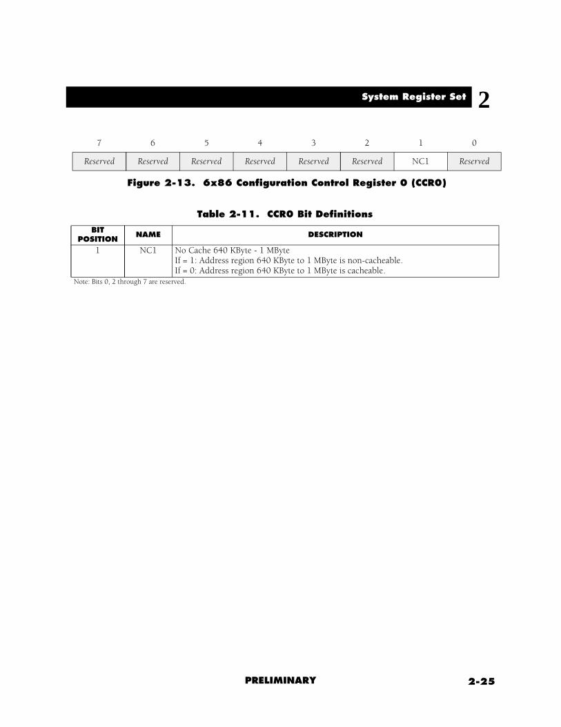
7 6 5 4 3 2 1 0
Reserved Reserved Reserved Reserved Reserved Reserved NC1 Reserved
Figure 2-13. 6x86 Configuration Control Register 0 (CCR0)
Table 2-11. CCR0 Bit Definitions
BITPOSITION
NAME DESCRIPTION
1 NC1 No Cache 640 KByte - 1 MByte If = 1: Address region 640 KByte to 1 MByte is non-cacheable.If = 0: Address region 640 KByte to 1 MByte is cacheable.
Note: Bits 0, 2 through 7 are reserved.

2-26 PRELIMINARY
System Register SetAdvancing the Standards
7 6 5 4 3 2 1 0
SM3 Reserved Reserved NO_LOCK Reserved SMAC USE_SMI Reserved
Figure 2-14. 6x86 Configuration Control Register 1 (CCR1)
Table 2-12. CCR1 Bit Definitions
BITPOSITION
NAME DESCRIPTION
1 USE_SMI Enable SMM and SMIACT# PinsIf = 1: SMI# and SMIACT# pins are enabled.If = 0: SMI# pin ignored and SMIACT# pin is driven inactive.
2 SMAC System Management Memory AccessIf = 1: Any access to addresses within the SMM address space, access system manage-ment memory instead of main memory. SMI# input is ignored. Used when initializing or testing SMM memory.If = 0: No effect on access.
4 NO_LOCK Negate LOCK#If = 1: All bus cycles are issued with LOCK# pin negated except page table accesses and interrupt acknowledge cycles. Interrupt acknowledge cycles are executed as locked cycles even though LOCK# is negated. With NO_LOCK set, previously noncacheable locked cycles are executed as unlocked cycles and therefore, may be cached. This results in higher performance. Refer to Region Control Registers for information on eliminating locked CPU bus cycles only in specific address regions.
7 SM3 SMM Address Space Address Region 3If = 1: Address Region 3 is designated as SMM address space.
Note: Bits 0, 3, 5 and 6 are reserved.

2-27
2
PRELIMINARY
System Register Set
7 6 5 4 3 2 1 0
USE_SUSP Reserved Reserved WPR1 SUSP_HLT LOCK_NW Reserved Reserved
Figure 2-15. 6x86 Configuration Control Register 2 (CCR2)
Table 2-13. CCR2 Bit Definitions
BITPOSITION
NAME DESCRIPTION
2 LOCK_NW Lock NW If = 1: NW bit in CR0 becomes read only and the CPU ignores any writes to the NW bit.If = 0: NW bit in CR0 can be modified.
3 SUSP_HLT Suspend on HaltIf = 1: Execution of the HLT instruction causes the CPU to enter low power sus-pend mode.
4 WPR1 Write-Protect Region 1 If = 1: Designates any cacheable accesses in 640 KByte to 1 MByte address region are write protected.
7 USE_SUSP Use Suspend Mode (Enable Suspend Pins)If = 1: SUSP# and SUSPA# pins are enabled.If = 0: SUSP# pin is ignored and SUSPA# pin floats.
Note: Bits 0,1, 5 and 6 are reserved.

2-28 PRELIMINARY
System Register SetAdvancing the Standards
7 6 5 4 3 2 1 0
MAPEN Reserved LINBRST NMI_EN SMI_LOCK
Figure 2-16. 6x86 Configuration Control Register 3 (CCR3)
Table 2-14. CCR3 Bit Definitions
BITPOSITION
NAME DESCRIPTION
0 SMI_LOCK SMI Lock If = 1: The following SMM configuration bits can only be modified while in an SMI service routine:CCR1: USE_SMI, SMAC, SM3CCR3: NMI_ENARR3: Starting address and block size.Once set, the features locked by SMI_LOCK cannot be unlocked until the RESET pin is asserted.
1 NMI_EN NMI EnableIf = 1: NMI interrupt is recognized while servicing an SMI interrupt.NMI_EN should be set only while in SMM, after the appropriate SMI interrupt service routine has been setup.
2 LINBRST If = 1: Use linear address sequence during burst cycles. If = 0: Use “1 + 4” address sequence during burst cycles. The “1 + 4” address sequence is compatible with Pentium’s burst address sequence.
4 - 7 MAPEN MAP EnableIf = 1h: All configuration registers are accessible.If = 0h: Only configuration registers with indexes C0-CFh, FEh and FFhare accessible.
Note: Bit 3 is reserved.
2-29
2
PRELIMINARY
System Register Set
.
7 6 5 4 3 2 1 0
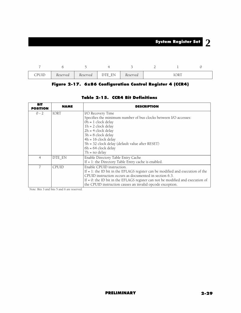
CPUID Reserved Reserved DTE_EN Reserved IORT
Figure 2-17. 6x86 Configuration Control Register 4 (CCR4)
Table 2-15. CCR4 Bit Definitions
BITPOSITION
NAME DESCRIPTION
0 - 2 IORT I/O Recovery TimeSpecifies the minimum number of bus clocks between I/O accesses:0h = 1 clock delay1h = 2 clock delay2h = 4 clock delay3h = 8 clock delay4h = 16 clock delay5h = 32 clock delay (default value after RESET)6h = 64 clock delay7h = no delay
4 DTE_EN Enable Directory Table Entry CacheIf = 1: the Directory Table Entry cache is enabled.
7 CPUID Enable CPUID instruction.If = 1: the ID bit in the EFLAGS register can be modified and execution of the CPUID instruction occurs as documented in section 6.3.If = 0: the ID bit in the EFLAGS register can not be modified and execution of the CPUID instruction causes an invalid opcode exception.
Note: Bits 3 and bits 5 and 6 are reserved.
2-30 PRELIMINARY
System Register SetAdvancing the Standards
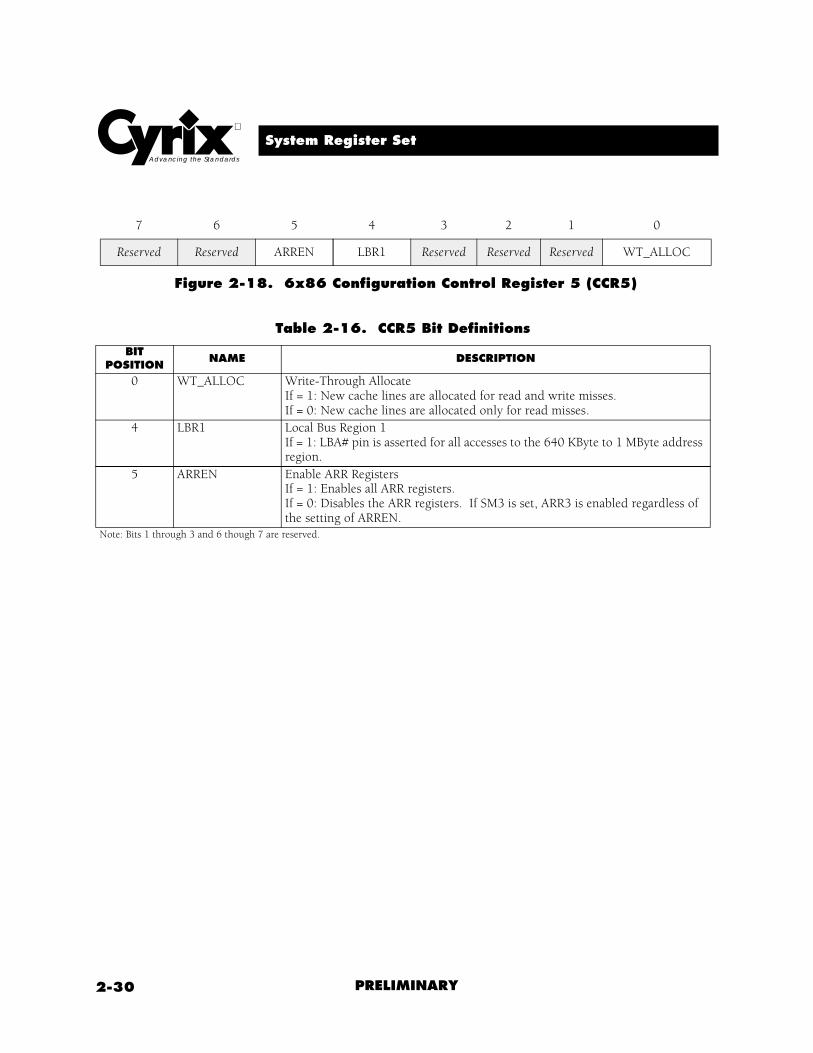
7 6 5 4 3 2 1 0
Reserved Reserved ARREN LBR1 Reserved Reserved Reserved WT_ALLOC
Figure 2-18. 6x86 Configuration Control Register 5 (CCR5)
Table 2-16. CCR5 Bit Definitions
BITPOSITION
NAME DESCRIPTION
0 WT_ALLOC Write-Through AllocateIf = 1: New cache lines are allocated for read and write misses. If = 0: New cache lines are allocated only for read misses.
4 LBR1 Local Bus Region 1If = 1: LBA# pin is asserted for all accesses to the 640 KByte to 1 MByte address region.
5 ARREN Enable ARR RegistersIf = 1: Enables all ARR registers.If = 0: Disables the ARR registers. If SM3 is set, ARR3 is enabled regardless of the setting of ARREN.
Note: Bits 1 through 3 and 6 though 7 are reserved.

2-31
2
PRELIMINARY
System Register Set
2.4.4.2 Address RegionRegisters
The Address Region Registers (ARR0 - ARR7)(Figure 2-19) are used to specify the location and size for the eight address regions.
Attributes for each address region are specified in the Region Control Registers (RCR0-RCR7). ARR7 and RCR7 are used to define system main memory and differ from ARR0-6 and RCR0-6.
With non-cacheable regions defined on-chip, the 6x86 CPU delievers optimum performance by using advanced techniques to eliminate data dependencies and resource conflicts in its exe-cution pipelines. If KEN# is active for accesses to regions defined as non-cacheable by the
RCRs, the region is not cached. The RCRs take precedence in this case.
A register index, shown in Table 2-17 (Page 2-32) is used to select one of three bytes in each ARR.
The starting address of the ARR address region, selected by the START ADDRESS field, must be on a block size boundary. For example, a 128 KByte block is allowed to have a starting address of 0 KBytes, 128 KBytes, 256 KBytes, and so on.
The SIZE field bit definition is listed in Table 2-18 (Page 2-32). If the SIZE field is zero, the address region is of zero size and thus disabled.
START ADDRESS SIZE
Memory Address Bits A31-A24
Memory Address Bits A23-A16
Memory Address Bits A15-A12
Size Bits 3-0
7 0 7 0 7 4 3 0
Figure 2-19. Address Region Registers (ARR0 - ARR7)

2-32 PRELIMINARY
System Register SetAdvancing the Standards
.
Table 2-17. ARR0 - ARR7 Register Index Assignments
ARRRegister
Memory Address (A31 - A24)
Memory Address (A23 - A16)
Memory Address(A15 - A12)
Address Region Size (3 - 0)
ARR0 C4h C5h C6h C6h
ARR1 C7h C8h C9h C9h
ARR2 CAh CBh CCh CCh
ARR3 CDh CEh CFh CFh
ARR4 D0h D1h D2h D2h
ARR5 D3h D4h D5h D5h
ARR6 D6h D7h D8h D8h
ARR7 D9h DAh DBh DBh
Table 2-18. Bit Definitions for SIZE Field
SIZE (3-0) BLOCK SIZE
SIZE (3-0)BLOCK SIZE
ARR0-6 ARR7 ARR0-6 ARR7
0h Disabled Disabled 8h 512 KBytes 32 MBytes
1h 4 KBytes 256 KBytes 9h 1 MBytes 64 MBytes
2h 8 KBytes 512 KBytes Ah 2 MBytes 128 MBytes
3h 16 KBytes 1 MBytes Bh 4 MBytes 256 MBytes
4h 32 KBytes 2 MBytes Ch 8 MBytes 512 MBytes
5h 64 KBytes 4 MBytes Dh 16 MBytes 1 GBytes
6h 128 KBytes 8 MBytes Eh 32 MBytes 2 GBytes
7h 256 KBytes 16 MBytes Fh 4 GBytes 4 GBytes
2-33
2
PRELIMINARY
System Register Set
2.4.4.3 Region Control Registers
The Region Control Registers (RCR0 - RCR7) specify the attributes associated with the ARRx address regions. The bit definitions for the region control registers are shown in Figure 2-20 (Page 2-34) and in Table 2-19 (Page 2-34). Cacheability, weak write ordering, weak locking, write gathering, cache write through policies and control of the LBA# pin can be activated or deactivated using the attribute bits.
If an address is accessed that is not in a memory region defined by the ARRx registers, the fol-lowing conditions will apply:
• LBA# pin is asserted• If the memory address is cached,
write-back is enabled if WB/WT# is returned high.
• Writes are not gathered• Strong locking takes place• Strong write ordering takes place• The memory access is cached, if KEN# is
returned asserted.
Overlapping Conditions Defined. If tworegions specified by ARRx registers overlap andconflicting attributes are specified, the follow-ing attributes take precedence:
• LBA# pin is asserted• Write-back is disabled• Writes are not gathered• Strong locking takes place• Strong write ordering takes place• The overlapping regions are
non-cacheable.
2-34 PRELIMINARY
System Register SetAdvancing the Standards
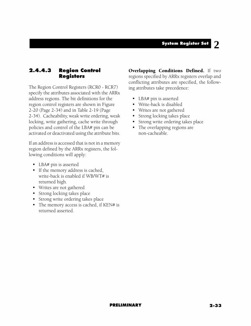
7 6 5 4 3 2 1 0
Reserved Reserved NLB WT WG WL WWO RCD / RCE*
*Note: RCD is defined for RCR0-RCR6. RCE is defined for RCR7.
Figure 2-20. Region Control Registers (RCR0-RCR7)
Table 2-19. RCR0-RCR7 Bit Definitions
RCRxBIT
POSITIONNAME DESCRIPTION
0 - 6 0 RCD If = 1: Disables caching for address region specified by ARRx.7 0 RCE If = 1: Enables caching for address region ARR7.
0 - 7 1 WWO If = 1: Weak write ordering for address region specified by ARRx.0 - 7 2 WL If = 1: Weak locking for address region specified by ARRx.0 - 7 3 WG If = 1: Write gathering for address region specified by ARRx.0 - 7 4 WT If = 1: Address region specified by ARRx is write-through.0 - 7 5 NLB If = 1:LBA# pin is not asserted for access to address region specified by ARRx
Note: Bits 6 and 7 are reserved.
Region Cache Disable (RCD). Setting RCD to a one defines the address region as non-cacheable. Whenever possible, the RCRs should be used to define non-cache-able regions rather than using external address decoding and driving the KEN# pin.
Region Cache Enable (RCE). Setting RCE to a one defines the address region as cache-able. RCE is used to define the system main memory as cacheable memory. It is implied that memory outside the region is non-cache-able.
Weak Write Ordering (WWO). Setting WWO=1 enables weak write ordering for that address region. Enabling WWO allows the 6x86 CPU to issue writes in its internal cache in an order different than their order in the code stream. External writes always occur in order (strong ordering). Therefore,
this should only be enabled for memory regions that are NOT sensitive to this condition. WWO should not be enabled for memory mapped I/O. WWO only applies to memory regions that have been cached and designated as write-back. It also applies to previously cached addresses even if the cache has been disabled (CD=1). Enabling WWO removes the write-ordering restriction and improves performance due to reduced pipeline stalls.
Weak Locking (WL). Setting WL=1 enables weak locking for that address region. With WL enabled, all bus cycles are issued with the LOCK# pin negated except for page table accesses and interrupt ackowleddge cycles. Interrupt acknowledge cycles are executed as locked cycles even though LOCK# is negated. With WL=1, previously non-cacheable locked cycles are exe-cuted as unlocked cycles and therefore, may be cached, resulting in higher performance. The

2-35
2
PRELIMINARY
System Register Set
NO_LOCK bit of CCR1 enables weak locking for the entire address space. The WL bit allows weak locking only for specific address regions. WL is independent of the cacheability of the address region.
Write Gathering (WG). Setting WG=1 enables write gathering for the associated address region. Write gathering allows multiple byte, word, or dword sequential address writes to accumulate in the on-chip write buffer. (As instructions are executed, the results are placed in a series of output buffers. These buffers are gathered into the finial output buffer).
When access is made to a non-sequential mem-ory location or when the 8-byte buffer becomes full, the contents of the buffer are written on the external 64-bit data bus. Performance is enhanced by avoiding as many as seven memory write cycles.
WG should not be used on memory regions that are sensitive to write cycle gathering. WG can be enabled for both cacheable and non-cacheable regions.
Write Through (WT). Setting WT=1 defines the address region as write-through instead of write-back, assuming the region is cacheable. Regions where system ROM are loaded (shad-owed or not) should be defined as write-through.
LBA# Not Asserted (NLB). Setting NLB=1 prevents the microprocessor from asserting the Local Bus Access (LBA#) output pin for accesses to that address region. The RCR regions may be used to define non-local bus address regions. The LBA# pin could then be asserted for all regions, except those defined by the RCRs. The LBA# signal may be used by the external hard-ware (e.g., chipsets) as an indication that local bus accesses are occurring.

2-36 PRELIMINARY
System Register SetAdvancing the Standards
2.4.4.4 Device Identification Registers
The Device Identification Registers (DIR0, DIR1) contain CPU identification, CPU stepping and CPU revision information. Bit definitions are shown in Figure 2-21, Table 2-20, Figure 2-22 and Table 2-21 respectively. Data in these registers cannot be changed. These registers can be read by using I/O ports 22 and 23. The register index for DIR0 is FEh and the register index for DIR1 is FFh.
7 0DEVID
Figure 2-21. Device Identification Register 0 (DIR0)
Table 2-20. DIR0 Bit Definitions
BITPOSITION
NAME DESCRIPTION
7 - 0 DEVID CPU Device Identification Number (read only).
7 4 3 0SID RID
Figure 2-22. Device Identification Register 1 (DIR1)
Table 2-21. DIR1 Bit Definitions
BITPOSITION
NAME DESCRIPTION
7 - 4 SID CPU Step Identification Number (read only).3 - 0 RID CPU Revision Identification (read only).

2-37
2
PRELIMINARY
System Register Set
2.4.5 Debug Registers
Six debug registers (DR0-DR3, DR6 and DR7), shown in Figure 2-23, support debugging on the 6x86 CPU. The bit definitions for the debug registers are listed in Table 2-22 (Page 2-38).
Memory addresses loaded in the debug regis-ters, referred to as “breakpoints”, generate a debug exception when a memory access of the specified type occurs to the specified address. A data breakpoint can be specified for a particular kind of memory access such as a read or a write. Code breakpoints can also be set allowing debug exceptions to occur whenever a given code access (execution) occurs.
The size of the debug target can be set to 1, 2, or 4 bytes. The debug registers are accessed via MOV instructions which can be executed only at privilege level 0.
The Debug Address Registers (DR0-DR3) each contain the linear address for one of four possi-ble breakpoints. Each breakpoint is further specified by bits in the Debug Control Register (DR7). For each breakpoint address in DR0-DR3, there are corresponding fields L, R/W, and LEN in DR7 that specify the type of memory access associated with the breakpoint.
The R/W field can be used to specify instruction execution as well as data access breakpoints. Instruction execution breakpoints are always taken before execution of the instruction that matches the breakpoint.
The Debug Status Register (DR6) reflects condi-tions that were in effect at the time the debug exception occurred. The contents of the DR6 register are not automatically cleared by the pro-cessor after a debug exception occurs and, therefore, should be cleared by software at the appropriate time.
DR7
DR6
DR3
DR2
DR1
DR0
1703203ALL BITS MARKED AS 0 OR 1 ARE RESERVED AND SHOULD NOT BE MODIFIED.
BREAKPOINT 3 LINEAR ADDRESS
BREAKPOINT 2 LINEAR ADDRESS
BREAKPOINT 1 LINEAR ADDRESS
BREAKPOINT 0 LINEAR ADDRESS
0 B B B B BB
0 100 0 0 0 0 0 0 0 0 0 0 0 0 0 0
LEN R/W LEN R/W LEN R/W LEN R/W0 0
G G L G L G L G L G L0 0 1
3 3 2 2
3 3 2 2 2 2 2 2 2 2 2 2 1 1 1 1 1 1 1 1 9 8 7 6 5 4 3 2 1 011 0 9 8 7 6 5 4 3 2 1 0 9 8 7
1 1 0
6 5 4 3 2 011
0
T S
D E E 3 3 2 2 1 1 0
3 2 1
0
01 1 1 1 1 1 1
Figure 2-23. Debug Registers

2-38 PRELIMINARY
System Register SetAdvancing the Standards
Code execution breakpoints may also be generated by placing the breakpoint instruction (INT 3) at the location where control is to be regained. Additionally, the single-step feature may be enabled by setting the TF flag in the EFLAGS register. This causes the processor to perform a debug excep-tion after the execution of every instruction.
Table 2-22. DR6 and DR7 Debug Register Field Definitions
REGISTER FIELDNUMBEROF BITS
DESCRIPTION
DR6 Bi 1 Bi is set by the processor if the conditions described by DRi, R/Wi, and LENi occurred when the debug exception occurred, even if the breakpoint is not enabled via the Gi or Li bits.
BT 1 BT is set by the processor before entering the debug handler if a task switch has occurred to a task with the T bit in the TSS set.
BS 1 BS is set by the processor if the debug exception was triggered by the single-step execution mode (TF flag in EFLAGS set).
DR7 R/Wi 2 Specifies type of break for the linear address in DR0, DR1, DR3, DR4:00 - Break on instruction execution only01 - Break on data writes only10 - Not used11 - Break on data reads or writes.
LENi 2 Specifies length of the linear address in DR0, DR1, DR3, DR4:00 - One byte length01 - Two byte length10 - Not used11 - Four byte length.
Gi 1 If set to a 1, breakpoint in DRi is globally enabled for all tasks and is not cleared by the processor as the result of a task switch.
Li 1 If set to a 1, breakpoint in DRi is locally enabled for the current task and is cleared by the processor as the result of a task switch.
GD 1 Global disable of debug register access. GD bit is cleared whenever a debug exception occurs.

2-39
2
PRELIMINARY
System Register Set
2.4.6 Test Registers
The test registers can be used to test the on-chip unified cache and to test the main TLB. The test registers are also used to enable 6x86 CPU vari-able-size paging.
Test registers TR3, TR4, and TR5 are used to test the unified cache. Use of these registers is described with the memory caches later in this chapter in Section 2.7.1.1.
Test registers TR6 and TR7 are used to test the TLB. Use of these test registers is described inSection 2.6.4.2.

2-40 PRELIMINARY
Address SpaceAdvancing the Standards
2.5 Address Space
The 6x86 CPU can directly address 64 KBytes of I/O space and 4 GBytes of physical memory (Figure 2-24).
Memory Address Space. Access can be made to memory addresses between 0000 0000h and FFFF FFFFh. This 4 GByte
Figure 2-24. Memory and I/O Address Spaces
FFFF FFFFh
Physical Memory
Physical
0000 0000h
64 KBytes
6x860000 FFFFh
0000 0000h
FFFF FFFFh
1730900
Memory Space
4 GBytes
I/O Address Space
ConfigurationRegister I/OSpace
0000 0023h0000 0022h
NotAccessible
memory space can be accessed using byte, word (16 bits), or doubleword (32 bits)format. Words and doublewords are stored in consecutive memory bytes with the low-order byte located in the lowest address. The phys-ical address of a word or doubleword is the byte address of the low-order byte.

2-41
2
PRELIMINARY
Memory Addressing Methods
I/O Address Space
The 6x86 I/O address space is accessed using IN and OUT instructions to addresses referred to as “ports”. The accessible I/O address space size is 64 KBytes and can be accessed through 8-bit, 16-bit or 32-bit ports. The execution of any IN or OUT instruction causes the M/IO# pin to be driven low, thereby selecting the I/O space instead of memory space.
The accessible I/O address space ranges between locations 0000 0000h and 0000 FFFFh (64 KBytes). The I/O locations (ports) 22h and 23h can be used to access the 6x86 configuration registers.
2.6 Memory AddressingMethods
With the 6x86 CPU, memory can be addressed using nine different addressing modes (Table 2-23, Page 2-42). These addressing modes are used to calculate an offset address often referred to as an effective address. Depending on the operating mode of the CPU, the offset is then combined using memory management mechanisms to create a physical address that actually addresses the physical memory devices.
Memory management mechanisms on the 6x86 CPU consist of segmentation and paging. Segmentation allows each program to use several independent, protected address spaces. Paging supports a memory subsystem that simulates a large address space using a small amount of RAM and disk storage for physical memory. Either or both of these mechanisms can be used for management of the 6x86 CPUmemory address space.

2-42 PRELIMINARY
Memory Addressing MethodsAdvancing the Standards
2.6.1 Offset Mechanism
The offset mechanism computes an offset (effective) address by adding together one or more of three values: a base, an index and a displacement. When present, the base is the value of one of the eight 32-bit general regis-ters. The index if present, like the base, is a value that is in one of the eight 32-bit general purpose registers (not including the ESP register). The index differs from the base in that the index is first multiplied by a scale factor of 1, 2, 4 or 8 before the summation is made. The third component added to the memory address calculation is the displace-ment. The displacement is a value of up to 32-bits in length supplied as part of the instruction. Figure 2-25 illustrates the calcula-tion of the offset address.
Nine valid combinations of the base, index, scale factor and displacement can be used with the 6x86 CPU instruction set. These combina-tions are listed in Table 2-23. The base and index both refer to contents of a register as indicated by [Base] and [Index].
Figure 2-25. Offset Address Calculation
Table 2-23. Memory Addressing Modes
ADDRESSINGMODE
BASE INDEXSCALE
FACTOR(SF)
DISPLACEMENT(DP)
OFFSET ADDRESS (OA)CALCULATION
Direct x OA = DP
Register Indirect x OA = [BASE]
Based x x OA = [BASE] + DP
Index x x OA = [INDEX] + DP
Scaled Index x x x OA = ([INDEX] * SF) + DP
Based Index x x OA = [BASE] + [INDEX]
Based Scaled Index x x x OA = [BASE] + ([INDEX] * SF)
Based Index withDisplacement
x x x OA = [BASE] + [INDEX] + DP
Based Scaled Index with Displacement
x x x x OA = [BASE] + ([INDEX] * SF) + DP
Index
Base Displacement
Scaling
Offset Address
1706603
x1, x2, x4, x8
(Effective Address)

2-43
2
PRELIMINARY
Memory Addressing Methods
2.6.2 MemoryAddressing
Real Mode Memory Addressing
In real mode operation, the 6x86 CPU only addresses the lowest 1 MByte of memory. To calculate a physical memory address, the 16-bit segment base address located in the selected segment register is multiplied by 16 and then the 16-bit offset address is added. The resulting 20-bit address is then extended.Three hexadecimal zeros are added as upper address bits to create the 32-bit physical address. Figure 2-26 illustrates the real mode address calculation.
The addition of the base address and the offset address may result in a carry. Therefore, the resulting address may actually contain up to 21 significant address bits that can address memory in the first 64 KBytes above 1 MByte.
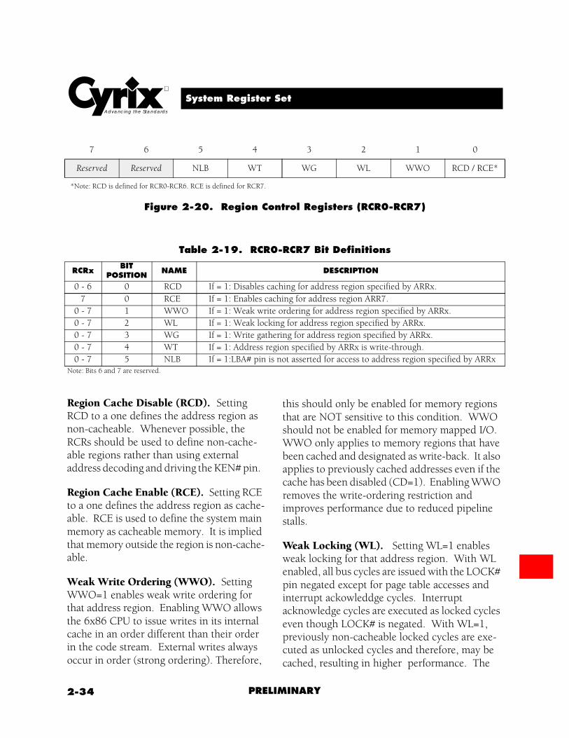
Protected Mode Memory Addressing
In protected mode three mechanisms calculate aphysical memory address (Figure 2-27, Page 2-44).
• Offset Mechanism that produces the offset or effective address as in real mode.
• Selector Mechanism that produces the base address.
• Optional Paging Mechanism that trans-lates a linear address to the physical memory address.
The offset and base address are added together to produce the linear address. If paging is not enabled, the linear address is used as the phys-ical memory address. If paging is enabled, the paging mechanism is used to translate the linear address into the physical address. The offset mechanism is described earlier in this section and applies to both real and protected mode. The selector and paging mechanisms are described in the following paragraphs.
Figure 2-26. Real Mode Address Calculation
Offset Mechanism
Selected Segment
Offset Address
1708304
X 16Register
+
16
16 20
20 32 Linear Address (Physical Address)
12
000h
2-44 PRELIMINARY
Memory Addressing MethodsAdvancing the Standards
Figure 2-27. Protected Mode Address Calculation
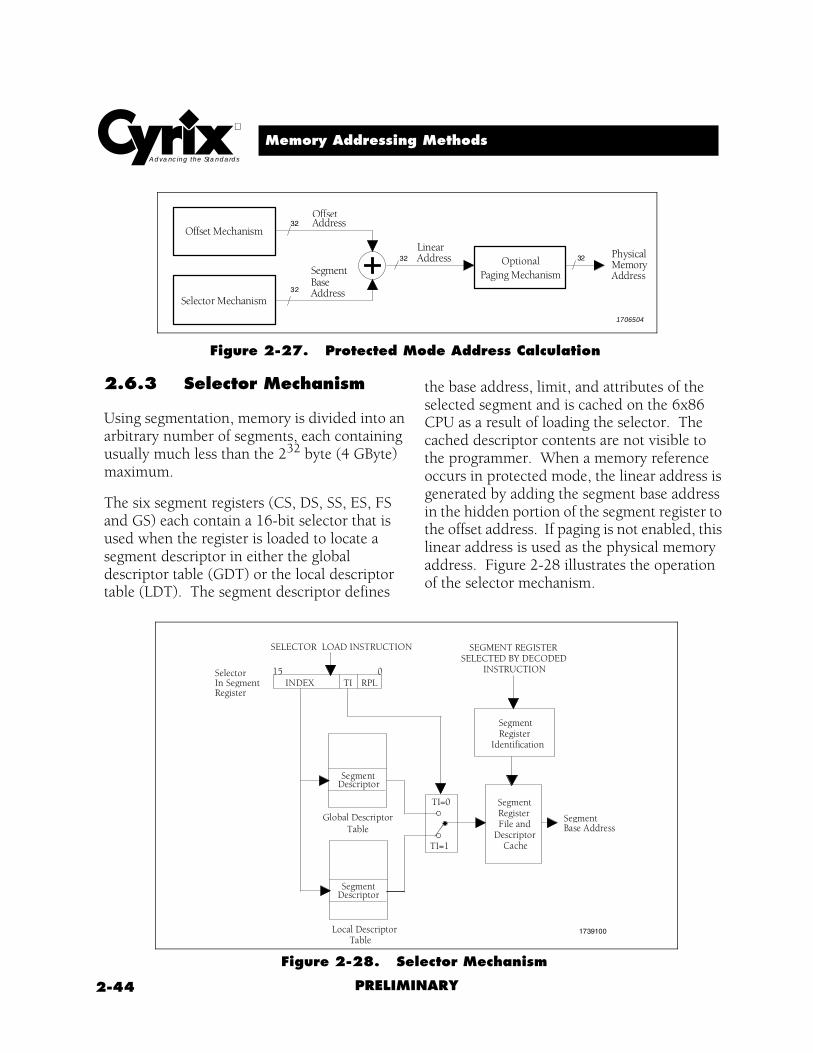
2.6.3 Selector Mechanism
Using segmentation, memory is divided into an arbitrary number of segments, each containing usually much less than the 232 byte (4 GByte) maximum.
The six segment registers (CS, DS, SS, ES, FS and GS) each contain a 16-bit selector that is used when the register is loaded to locate a segment descriptor in either the global descriptor table (GDT) or the local descriptor table (LDT). The segment descriptor defines
the base address, limit, and attributes of the selected segment and is cached on the 6x86 CPU as a result of loading the selector. The cached descriptor contents are not visible to the programmer. When a memory reference occurs in protected mode, the linear address is generated by adding the segment base address in the hidden portion of the segment register to the offset address. If paging is not enabled, this linear address is used as the physical memory address. Figure 2-28 illustrates the operation of the selector mechanism.
Figure 2-28. Selector Mechanism
Offset Mechanism
Selector Mechanism
OptionalPhysical
1706504
Paging MechanismMemoryAddress
32
32
32 32
OffsetAddress
Address
Linear Address
SegmentBase
Segment
15 0
1739100
INDEX TI RPL
Descriptor
SegmentDescriptor
TI=0
TI=1
Local Descriptor Table
SELECTOR LOAD INSTRUCTION SEGMENT REGISTERSELECTED BY DECODED
INSTRUCTION
SegmentRegisterFile and
DescriptorCache
SegmentRegister
Identification
SelectorIn SegmentRegister
Global Descriptor Table
SegmentBase Address

2-45
2
PRELIMINARY
Memory Addressing Methods
2.6.4 Paging Mechanisms
The paging mechanisms (Figure 2-29) trans-late linear addresses to their corresponding physical addresses. For traditional paging, the page size is always 4 KBytes. If 6x86 Variable-Size Paging is selected, a page size may be as large as 4 GBytes. Use of larger page sizes allows large memory areas such as video memory to be placed in a single page, elimi-nating page table thrashing.
Paging is activated when the PG and the PE bits within the CR0 register are set.
2.6.4.1 Traditional PagingMechanism
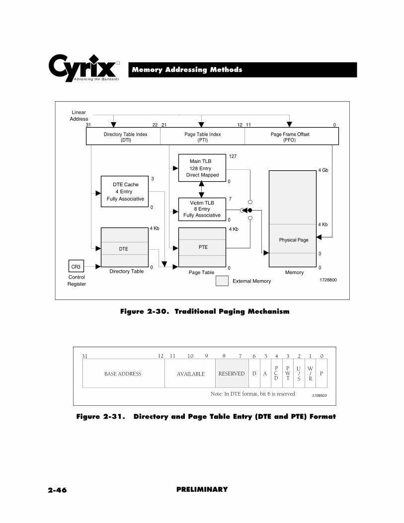
The traditional paging mechanism translates the 20 most significant bits of a linear address to a physical address. The linear address is divided into three fields DTI, PTI, PFO (Figure 2-30, Page 2-46). These fields respectively select:
• an entry in the directory table,• an entry in the page table selected by the
directory table• the offset in the physical page selected by
the page table
The directory table and all the page tables can be considered as pages as they are 4-KBytes in
size and are aligned on 4-KByte boundaries.Each entry in these tables is 32 bits in length. The fields within the entries are detailed in Figure 2-31 (Page 2-46) and Table 2-24 (Page 2-47).
A single page directory table can address up to 4 GBytes of virtual memory (1,024 page tables—each table can select 1,024 pages and each page contains 4 KBytes).
Translation Lookaside Buffer (TLB) is made up of three caches (Figure 2-30, Page 2-46).
• the DTE Cache caches directory table entries
• the Main TLB caches page tables entries• the Victim TLB stores PTEs that have been
evicted from the Main TLB
The DTE cache is a 4-entry fully associative cache, the main TLB is a 128-entry direct mapped cache and the victim TLB is an 8-entry fully associative cache.The DTE cache caches the four most recent DTEs so that future TLB misses only require a single page table read to calculate the physical address. The DTE cache is disabled following RESET and is enabled by setting the DTE_EN bit (CCR4 bit4).
Figure 2-29. Paging Mechanisms
1739600
Physical AddressLinear Address
Variable-Size Paging Mechanism
Traditional PagingMechanism
2-46 PRELIMINARY
Memory Addressing MethodsAdvancing the Standards
Figure 2-30. Traditional Paging Mechanism
BASE ADDRESS AVAILABLE PWU
D
31 012 11 9 8 123456710
A
1708503
PPCD
WT
/S
/R
Note: In DTE format, bit 6 is reserved
RESERVED
Figure 2-31. Directory and Page Table Entry (DTE and PTE) Format
CR3
1728800
Directory Table Index Page Table Index Page Frame Offset
31 22 21 12 11 0
Physical Page
DTE PTE
0 0 0
4 Kb4 Kb
(DTI) (PTI) (PFO)
7
0
0
127
0
3
Main TLB128 Entry
Direct Mapped
DTE Cache4 Entry
Fully Associative
Page Table MemoryDirectory Table
0
4 Kb
4 Gb
Linear Address
ControlRegister
Victim TLB8 Entry
Fully Associative
External Memory

2-47
2
PRELIMINARY
Memory Addressing Methods
Table 2-24. Directory and Page Table Entry (DTE and PTE) Bit Definitions
BIT POSITION FIELD NAME DESCRIPTION
31-12 BASEADDRESS
Specifies the base address of the page or page table.
11-9 -- Undefined and available to the programmer.
8-7 -- Reserved and not available to the programmer.
6 D Dirty Bit. If set, indicates that a write access has occurred to the page (PTE only, undefined in DTE).
5 A Accessed Flag. If set, indicates that a read access or write access has occurredto the page.
4 PCD Page Caching Disable Flag. If set, indicates that the page is not cacheable inthe on-chip cache.
3 PWT Page Write-Through Flag. If set, indicates that writes to the page or page tables that hit in the on-chip cache must update both the cache and external memory.
2 U/S User/Supervisor Attribute. If set (user), page is accessible at privilege level 3. If clear (supervisor), page is accessible only when CPL ≤ 2.
1 W/R Write/Read Attribute. If set (write), page is writable. If clear (read), page is read only.
0 P Present Flag. If set, indicates that the page is present in RAM memory, andvalidates the remaining DTE/PTE bits. If clear, indicates that the page is notpresent in memory and the remaining DTE/PTE bits can be used by theprogrammer.
For a TLB hit, the TLB eliminates accesses to external directory and page tables.
The victim TLB increases the apparent associa-tivity of the main TLB and helps eliminate TLB trashing (unproductive TLB management). When an entry in the main TLB is replaced, a copy of the replaced entry is sent to the victim TLB before the entry in the main TLB is over-written. If the victim TLB receives a hit, its entry is swapped with a main TLB entry.
The TLB must be flushed by the software when entries in the page tables are changed. The TLB
is flushed whenever the CR3 register is loaded. A particular page can be flushed from the TLB by using the INVLPG instruction. This instruc-tion also flushes the entire DTE cache.
2.6.4.2 Translation LookasideBuffer Testing
The TLB can be tested by writing to a main TLB followed by performing a TLB lookup (TLB read) to see if the expected contents are within the TLB. TLB test operations are performed using test register TR6 and TR7 shown inFigure 2-32 (Page 2-48). Tables 2-25 through 2-27 list the bit definitions for TR6 and TR7.

2-48 PRELIMINARY
Memory Addressing MethodsAdvancing the Standards
Main TLB Write. To perform a direct write to a main TLB entry, the TR7 register is config-ured with the desired physical address as well as the PCD and PWT bits. The BI, HV, HD and HB bits are not used. The TR6 register is then configured with the linear address, D, U, W and V bits. The D, U, and W bits must be com-plements of the D#, U#, and W# bits during a write. When the TR6 register is configured, the 6x86 CPU writes the linear and physical address into the main TLB along with the A, D, U, and W bits. The main TLB entry is selected by bits 12 through 18 of the linear address field.
TLB Lookup. During a TLB lookup, the 6x86 CPU queries the TLB with a given linear address and expected A, W, U and D values. The query returns a corresponding physical address, and the source of the address. The
address source could be from the main TLB, from the victim TLB or from the variable-size paging mechanism.
The TLB lookup involves a single TR6 register write. The CMD bits are set to 0x1. The D, U, W, D#, U# and W# bits are not used during TLB lookups.
After a TLB lookup, the HV, HD and HB bits in TR7 indicate which (if any) PTEs were found with the requested linear address. If a TLB entry was found for a PTE in the victim or vari-able size-paging cache, the BI bit in the TR7 register will contain the index of the particular entry. If multiple entries respond, only the HV, HD and HB bits are valid and all TR7 fields are undefined.
Figure 2-32. TLB Test Registers
ADR6 (LINEAR ADDRESS)
= Reserved
V D U U# W TR6
1729100
ADR7 (PHYSICAL ADDRESS / BC MASK)
31 12 10 9 8 7 6 5
PCD PWT HV TR7BI HD
4 3 2 01
D# W#
12 10 9 8 7 6 5 4 3 2 0131
11
11
CMD
HB
A A#
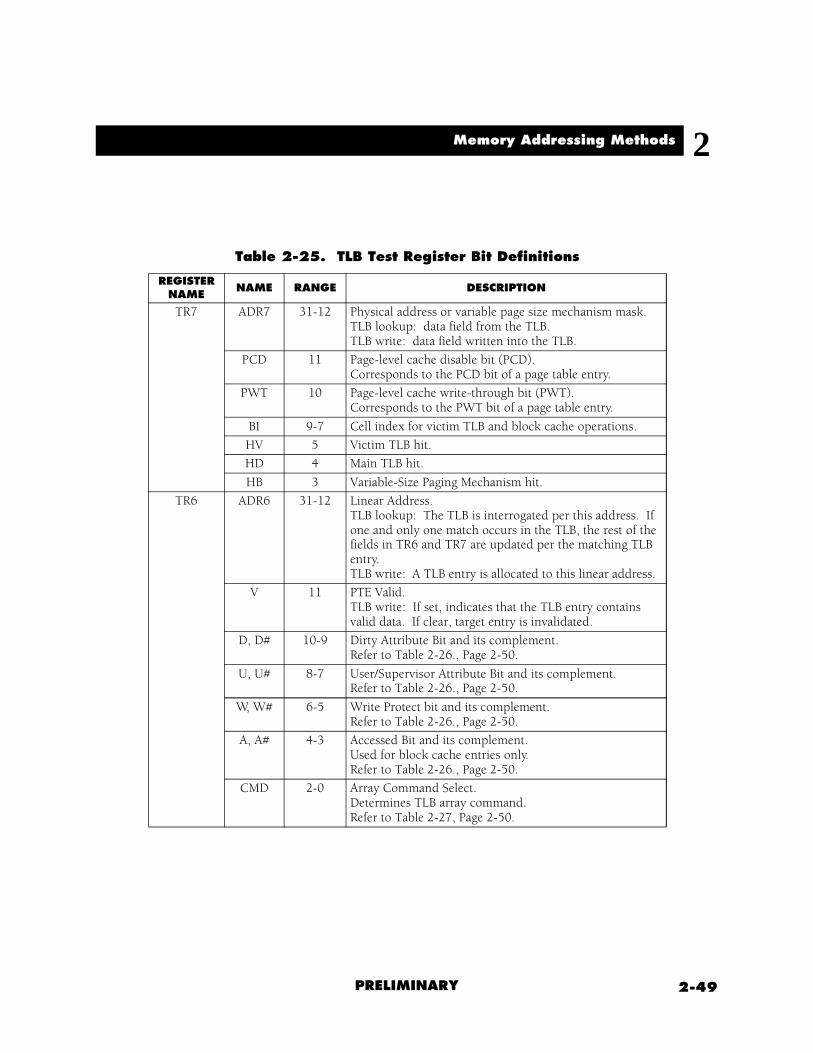
2-49
2
PRELIMINARY
Memory Addressing Methods
Table 2-25. TLB Test Register Bit Definitions
REGISTERNAME
NAME RANGE DESCRIPTION
TR7 ADR7 31-12 Physical address or variable page size mechanism mask.TLB lookup: data field from the TLB.TLB write: data field written into the TLB.
PCD 11 Page-level cache disable bit (PCD).Corresponds to the PCD bit of a page table entry.
PWT 10 Page-level cache write-through bit (PWT).Corresponds to the PWT bit of a page table entry.
BI 9-7 Cell index for victim TLB and block cache operations.
HV 5 Victim TLB hit.
HD 4 Main TLB hit.
HB 3 Variable-Size Paging Mechanism hit.
TR6 ADR6 31-12 Linear Address. TLB lookup: The TLB is interrogated per this address. If one and only one match occurs in the TLB, the rest of the fields in TR6 and TR7 are updated per the matching TLB entry.TLB write: A TLB entry is allocated to this linear address.
V 11 PTE Valid.TLB write: If set, indicates that the TLB entry contains valid data. If clear, target entry is invalidated.
D, D# 10-9 Dirty Attribute Bit and its complement. Refer to Table 2-26., Page 2-50.
U, U# 8-7 User/Supervisor Attribute Bit and its complement.Refer to Table 2-26., Page 2-50.
W, W# 6-5 Write Protect bit and its complement.Refer to Table 2-26., Page 2-50.
A, A# 4-3 Accessed Bit and its complement.Used for block cache entries only.Refer to Table 2-26., Page 2-50.
CMD 2-0 Array Command Select.Determines TLB array command.Refer to Table 2-27, Page 2-50.

2-50 PRELIMINARY
Memory Addressing MethodsAdvancing the Standards
Table 2-26. TR6 Attribute Bit Pairs
BIT BIT# EFFECT ON TLB LOOKUP EFFECT ON TLB WRITE
0 0 Do not match. Undefined.
0 1 If bit = 0, match. Bit is cleared.
1 0 If bit = 1, match. The bit is set.
1 1 If bit = 0 or 1, match. Undefined.Note: “BIT” applies to A, D, U or W fields in TR6; “BIT#” applies to A#, D#, U#, or W# fields in TR6.
Table 2-27. TR6 Command Bits
CMD Command
0x0 Direct write to main TLB.
0x1 TLB lookup for a linear address in all arrays.
100 Write to variable page size mask only.
110 Write to variable page size linear and physical address fields.
101 Read variable page size mask and linear address.
111 Read variable page size cache physical and linear address.Note: x = don’t care

2-51
2
PRELIMINARY
Memory Addressing Methods
2.6.5 Variable-SizePaging Mechanism
The Variable-Size Paging Mechanism (VSPM) is an advanced alternative to traditional paging. As shown in Figure 2-33, VSPM allows the creation of pages ranging in size from 4 KBytes to 4 GBytes. The larger page size nearly eliminates page table thrashing associated with using multiple 4-KByte pages.
For example, paging 1 MByte of memory requires 256 4-KByte pages using traditional paging. The software not only incurs overhead during setting up the 256 pages, but also incurs additional overhead accessing the page tables each time a page is not found in the on-chip TLB. In contrast, a single 1-MByte page virtually eliminates the overhead.
Configuring Variable-Size Pages. The VSPM is configured using TLB test registers, TR6 and TR7 (These registers are also used to test the TLB). The VSPM configuration is performed in much the same manner as when writing to a line of the TLB (Refer to Section 2.6.4.2.). The major exception to this, is that a mask field is written to the VSPM as part of the VSPM configuration.
The physical address, linear address, valid bit and attribute bits in a main TLB write all have the same meaning as in a main TLB read except that CMD=110. The BI field is used to select the VSPM cell to be written.
A VSPM mask setup operation is performed when CMD=100 and a test register write is per-formed. During a VSPM mask setup, the TR7 address field is used as the mask field. The mask field selectively masks linear address bits 31-12 from the VSPM tag compare. This has the effect of allowing the VSPM to map pages greater than 4 KBytes.
Figure 2-33. Variable-Size Paging Mechanism
1739200
Physical Page
0Memory
0
< 4 GByte
4 GByteLinear
Address
Variable-Size Paging Mechanism
PhysicalAddress
2-52 PRELIMINARY
Memory CachesAdvancing the Standards
After a VSPM mask setup, the valid bit, attribute bits, and the linear address are left in undefined states. Therefore, the VSPM mask setup should be performed prior to other VSPM operations.
Unlike the victim and main TLBs, the VSPM operations make use of the accessed bit. During a VSPM mask or physical address write the A and A# fields are written to the VSPM.
VSPM Reads. VSPM reads are performed with the address of the entry to be read in the BI field of the TR7 register and with CMD=111. The entry’s and physical address is read into the TR6 and TR7 address fields as well as the valid bit, and attribute bits.
If CMD=101, the linear address, mask, valid bit and attribute bits are read.
2.7 Memory Caches
The 6x86 CPU contains two memory caches as described in Chapter 1. The Unified Cache acts the primary data cache, and secondary instruc-tion cache. The Instruction Line Cache is the primary instruction cache and provides a high speed instruction stream for the Integer Unit.
The unified cache is dual-ported allowing simultaneous access to any two unique banks. Two different banks may be accessed at the same time permitting any two of the following operations to occur in parallel:
• Code fetch• Data read (X pipe, Y pipe or FPU)• Data write (X pipe, Y pipe or FPU).
2.7.1 Unified Cache MESI States
The unified cache lines are assigned one of four MESI states as determined by MESI bits stored in tag memory. Each 32-byte cache line is divided into two 16-byte sectors. Each sector contains its own MESI bits. The four MESI states are described below:
Modified MESI cache lines are those that have been updated by the CPU, but the corre-sponding main memory location has not yet been updated by an external write cycle. Modi-fied cache lines are referred to as dirty cache lines.
Exclusive MESI lines are lines that are exclusive to the 6x86 CPU and are not duplicated within another caching agent’s cache within the same system. A write to this cache line may be performed without issuing an external write cycle.
Shared MESI lines may be present in another caching agent’s cache within the same system. A write to this cache line forces a corresponding external write cycle.
Invalid MESI lines are cache lines that do not contain any valid data.

2-53
2
PRELIMINARY
Memory Caches
2.7.1.1 Unified Cache Testing
The unified cache can be tested through the use of TR3, TR4, and TR5 on-chip test regis-ters. Fields within these test registers identify which area of the cache will be selected for testing.
Cache Organization. The unified cache (Figure 2-34) is divided into 32-bytes lines. This cache is divided into four sets. Since a set (as well as the cache) is smaller than main memory, each line in the set corresponds to more than one line in main memory. When a cache line is allocated, bits A31-A12 of the main memory address are stored in the cache
line tag. The remaining address bits are used to identify the specific 32-byte cache line (A11-A5), and the specific 4-byte entry within the cache line (A4-A2).
Test Initiation. A test register operation is initiated by writing to the TR5 register shown in Figure 2-35 (Page 2-54) using a special MOV instruction. The TR5 CTL field, detailed in Table 2-28 (Page 2-54), determines the function to be performed. For cache writes, the registers TR4 and TR3 must be initialized before a write is made to TR5. Eight 4-byte accesses are required to access a complete cache line.
Figure 2-34. Unified Cache
1739700
SET 0
SET 1
SET 2
SET 3
ENT = 4-byte entry
32 Bytes of Data
512 Lines
ENT ENT ENT ENT ENT ENT ENT ENT
Lower SectorUpper Sector
128 Lines
TypicalSingleLine

2-54 PRELIMINARY
Memory CachesAdvancing the Standards
Figure 2-35. Cache Test Registers
= Reserved1729400
31
TR5
DATA (CACHE DATA)
31
MESIL TR4
31
TR3
0
CTL
MRUTAG (CACHE TAG ADDRESS)
11 10 9 8 7 6 5 4 3 2 01
9 8 7 6 5 4 3 2 01
1213
LINESET ENT
11 1012
MESIU
Table 2-28. Cache Test Register Bit Definitions
REGISTERNAME
FIELDNAME
RANGE DESCRIPTION
TR5 SET 13 - 12 Cache set selection (one of four “sets”).
LINE 11 - 5 Cache line selection (one of 128 lines).
ENT 4 - 2 Entry selection (one of eight 4-byte entries in a line).
CTL 1 - 0 Control fieldIf = 00: flush cache without invalidateIf = 01: write cacheIf = 10: read cacheIf = 11: no cache or test register modification
TR4 TAG 31 - 12 Physical address for selected line
MESIU 7 - 6 If = 00, Modified Upper Sector MESI bitsIf = 01, Shared Upper Sector MESI bitsIf = 10, Exclusive Upper Sector MESI bitsIf = 11, Invalid Upper Sector MESI bits*
MESIL 5 - 4 If = 00, Modified Lower Sector MESI bitsIf = 01, Shared Lower Sector MESI bitsIf = 10, Exclusive Lower Sector MESI bitsIf = 11, Invalid Lower Sector MESI bits*
MRU 3 - 0 Used to determine the Least Recently Used (LRU) line.
TR3 DATA 31 - 0 Data written or read during a cache test.*Note: All 32 bytes should contain valid data before a line is marked as valid.
2-55
2
PRELIMINARY
Interrupts and Exceptions
Write Operations. During a write, the TR3 DATA (32-bits) and TAG field information is written to the address selected by the SET, LINE, and ENT fields in TR5.
Read Operations. During a read, the cache address selected by the SET, LINE and ENT fields in TR5 are used to read data into the TR3 DATA (32-bits) field. The TAG, MESI and MRU fields in TR4 are updated with the information from the selected line. TR3 holds the selected read data.
Cache Flushing. A cache flush occurs during a TR5 write if the CTL field is set to zero. During flushing, the CPU’s cache controller reads through all the lines in the cache. “Modi-fied” lines are redefined as “shared” by setting the shared MESI bit. Clean lines are left in their original state.
2.8 Interrupts andExceptions
The processing of either an interrupt or an exception changes the normal sequential flow of a program by transferring program control to a selected service routine. Except for SMM interrupts, the location of the selected service routine is determined by one of the interrupt vectors stored in the interrupt descriptor table.
Hardware interrupts are generated by signal sources external to the CPU. All exceptions (including so-called software interrupts) are produced internally by the CPU.
2.8.1 Interrupts
External events can interrupt normal program execution by using one of the three interrupt pins on the 6x86 CPU.
• Non-maskable Interrupt (NMI pin)• Maskable Interrupt (INTR pin)• SMM Interrupt (SMI# pin).
For most interrupts, program transfer to the interrupt routine occurs after the current instruction has been completed. When the execution returns to the original program, it beginsimmediately following the last completed instruc-tion.
With the exception of string operations, inter-rupts are acknowledged between instruc-tions. Long string operations have interrupt windows between memory moves that allow interrupts to be acknowledged.
The NMI interrupt cannot be masked by software and always uses interrupt vector 2 to locate its service routine. Since the interrupt vector is fixed and is supplied internally, no interrupt acknowledge bus cycles are performed. This interrupt is normally reserved for unusual situations such as parity errors and has priority over INTR interrupts.
Once NMI processing has started, no addi-tional NMIs are processed until an IRET instruction is executed, typically at the end of the NMI service routine. If NMI is re-asserted prior to execution of the IRET instruction, one and only one NMI rising edge is stored andprocessed after execution of the next IRET.
2-56 PRELIMINARY
Interrupts and ExceptionsAdvancing the Standards
2.8.2 Exceptions
Exceptions are generated by an interrupt instruction or a program error. Exceptions are classified as traps, faults or aborts depending on the mechanism used to report them and the restartability of the instruction that first caused the exception.
A Trap Exception is reported immediately following the instruction that generated the trap exception. Trap exceptions are generated by execution of a software interrupt instruction (INTO, INT 3, INT n, BOUND), by a single-step operation or by a data breakpoint.
Software interrupts can be used to simulate hardware interrupts. For example, an INT n instruction causes the processor to execute the interrupt service routine pointed to by the nth vector in the interrupt table. Execution of the interrupt service routine occurs regardless of the state of the IF flag in the EFLAGS register.
The one byte INT 3, or breakpoint interrupt (vector 3), is a particular case of the INT n instruction. By inserting this one byte instruc-tion in a program, the user can set breakpoints in the code that can be used during debug.
Single-step operation is enabled by setting the TF bit in the EFLAGS register. When TF is set, the CPU generates a debug exception (vector 1)after the execution of every instruction. Data breakpoints also generate a debug exception and are specified by loading the debug regis-ters (DR0-DR7) with the appropriate values.
During the NMI service routine, maskable interrupts may be enabled (unmasked). If an unmasked INTR occurs during the NMI service routine, the INTR is serviced and execution returns to the NMI service routine following the next IRET. If a HALT instruction is executed within the NMI service routine, the 6x86 CPU restarts execution only in response to RESET, an unmasked INTR or an SMM inter-rupt. NMI does not restart CPU execution under this condition.
The INTR interrupt is unmasked when the Interrupt Enable Flag (IF) in the EFLAGS register is set to 1. When an INTR interrupt occurs, the CPU performs two locked interrupt acknowledge bus cycles. During the second cycle, the CPU reads an 8-bit vector that is supplied by an external interrupt controller. This vector selects one of the 256 possible interrupt handlers which will be executed in response to the interrupt.
The SMM interrupt has higher priority than either INTR or NMI. After SMI# is asserted, program execution is passed to an SMI service routine that runs in SMM address space reserved for this purpose. The remainder of this section does not apply to the SMM inter-rupts. SMM interrupts are described in greater detail later in this chapter.
2-57
2
PRELIMINARY
Interrupts and Exceptions
A Fault Exception is reported prior to completion of the instruction that generated the exception. By reporting the fault prior to instruction completion, the CPU is left in a state that allows the instruction to be restarted and the effects of the faulting instruction to be nullified. Fault exceptions include divide-by-zero errors, invalid opcodes, page faults and coprocessor errors. Instruction breakpoints (vector 1) are also handled as faults. After execution of the fault service routine, the instruction pointer points to the instruction that caused the fault.
An Abort Exception is a type of fault exceptionthat is severe enough that the CPU cannot restartthe program at the faulting instruction. The double fault (vector 8) is the only abort excep-tion that occurs on the 6x86 CPU.
2.8.3 Interrupt Vectors
When the CPU services an interrupt or excep-tion, the current program’s FLAGS, code segment and instruction pointer are pushed onto the stack to allow resumption of execu-tion of the interrupted program. In protected mode, the processor also saves an error code for some exceptions. Program control is then transferred to the interrupt handler (also called the interrupt service routine). Upon execution of an IRET at the end of the service routine, program execution resumes by popping from the stack, the instruction pointer, code segment, and FLAGS.
Interrupt Vector Assignments
Each interrupt (except SMI#) and exception is assigned one of 256 interrupt vector numbers (Table 2-29). The first 32 interrupt vector assignments are defined or reserved. INT instructions acting as software interrupts may use any of the interrupt vectors, 0 through 255.

2-58 PRELIMINARY
Interrupts and ExceptionsAdvancing the Standards
Table 2-29. Interrupt Vector Assignments
INTERRUPT VECTOR FUNCTION EXCEPTION TYPE
0 Divide error FAULT
1 Debug exception TRAP/FAULT*
2 NMI interrupt
3 Breakpoint TRAP
4 Interrupt on overflow TRAP
5 BOUND range exceeded FAULT
6 Invalid opcode FAULT
7 Device not available FAULT
8 Double fault ABORT
9 Reserved
10 Invalid TSS FAULT
11 Segment not present FAULT
12 Stack fault FAULT
13 General protection fault TRAP/FAULT
14 Page fault FAULT
15 Reserved
16 FPU error FAULT
17 Alignment check exception FAULT
18-31 Reserved
32-255 Maskable hardware interrupts TRAP
0-255 Programmed interrupt TRAP*Note: Data breakpoints and single-steps are traps. All other debug exceptions are faults.

2-59
2
PRELIMINARY
Interrupts and Exceptions
In response to a maskable hardware interrupt (INTR), the 6x86 CPU issues interrupt acknowledge bus cycles used to read the vectornumber from external hardware. These vectorsshould be in the range 32 - 255 as vectors 0 - 31are reserved.
Interrupt Descriptor Table
The interrupt vector number is used by the 6x86 CPU to locate an entry in the interrupt descriptor table (IDT). In real mode, each IDT entry consists of a four-byte far pointer to the beginning of the corresponding interrupt service routine. In protected mode, each IDT entry is an eight-byte descriptor. The Interrupt Descriptor Table Register (IDTR) specifies the beginning address and limit of the IDT. Following reset, the IDTR contains a base address of 0h with a limit of 3FFh.
The IDT can be located anywhere in physical memory as determined by the IDTR register. The IDT may contain different types of descrip-tors: interrupt gates, trap gates and task gates. Interrupt gates are used primarily to enter a hardware interrupt handler. Trap gates are generally used to enter an exception handler or software interrupt handler. If an interrupt gate is used, the Interrupt Enable Flag (IF) in the EFLAGS register is cleared before the interrupt handler is entered. Task gates are used to make the transition to a new task.
2.8.4 Interrupt and ExceptionPriorities
As the 6x86 CPU executes instructions, it follows a consistent policy for prioritizing exceptions and hardware interrupts. The priori-ties for competing interrupts and exceptions are listed in Table 2-30 (Page 2-60). Debug traps for the previous instruction and the next instructions always take precedence. SMM interrupts are the next priority. When NMI and maskable INTR interrupts are both detected at the same instruction boundary, the 6x86 micro-processor services the NMI interrupt first.
The 6x86 CPU checks for exceptions in parallel with instruction decoding and execution. Several exceptions can result from a single instruction. However, only one exception is generated upon each attempt to execute the instruction. Each exception service routine should make the appropriate corrections to the instruction and then restart the instruction. In this way, exceptions can be serviced until the instruction executes properly.
The 6x86 CPU supports instruction restart after all faults, except when an instruction causes a task switch to a task whose task state segment (TSS) is partially not present. A TSS can be partially not present if the TSS is not page aligned and one of the pages where the TSS resides is not currently in memory.

2-60 PRELIMINARY
Interrupts and ExceptionsAdvancing the Standards
Table 2-30. Interrupt and Exception Priorities
PRIORITY DESCRIPTION NOTES
0 Warm Reset Caused by the assertion of WM_RST.
1 Debug traps and faults from previ-ous instruction.
Includes single-step trap and data breakpoints specified in the debug registers.
2 Debug traps for next instruction. Includes instruction execution breakpoints specified in the debug registers.
3 Hardware Cache Flush Caused by the assertion of FLUSH#.
4 SMM hardware interrupt. SMM interrupts are caused by SMI# asserted and always have highest priority.
5 Non-maskable hardware interrupt. Caused by NMI asserted.
6 Maskable hardware interrupt. Caused by INTR asserted and IF = 1.
7 Faults resulting from fetching the next instruction.
Includes segment not present, general protec-tion fault and page fault.
8 Faults resulting from instruction decoding.
Includes illegal opcode, instruction too long, or privilege violation.
9 WAIT instruction and TS = 1 and MP = 1.
Device not available exception generated.
10 ESC instruction and EM = 1 or TS = 1.
Device not available exception generated.
11 Floating point error exception. Caused by unmasked floating point exception with NE = 1.
12 Segmentation faults (for each memory reference required by the instruction) that prevent transfer-ring the entire memory operand.
Includes segment not present, stack fault, and general protection fault.
13 Page Faults that prevent transfer-ring the entire memory operand.
14 Alignment check fault.

2-61
2
PRELIMINARY
Interrupts and Exceptions
2.8.5 Exceptions in Real Mode
Many of the exceptions described in Table 2-30 (Page 2-60) are not applicable in real mode. Exceptions 10, 11, and 14 do not occur in real mode. Other exceptions have slightly different meanings in real mode as listed in Table 2-31.
Table 2-31. Exception Changes in Real Mode
VECTOR NUMBER
PROTECTED MODE FUNC-TION
REAL MODE FUNCTION
8 Double fault. Interrupt table limit overrun.
10 Invalid TSS. x
11 Segment not present. x
12 Stack fault. SS segment limit overrun.
13 General protection fault. CS, DS, ES, FS, GS segment limit overrun.
14 Page fault. xNote: x = does not occur
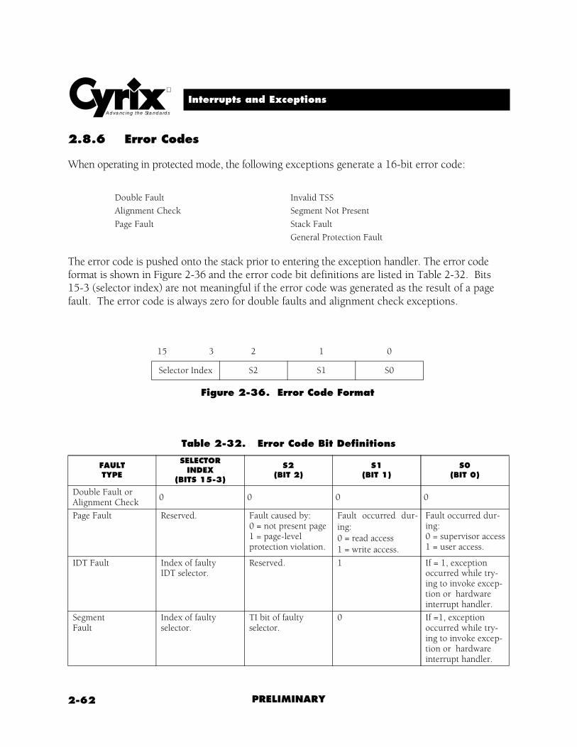
2-62 PRELIMINARY
Interrupts and ExceptionsAdvancing the Standards
2.8.6 Error Codes
When operating in protected mode, the following exceptions generate a 16-bit error code:
The error code is pushed onto the stack prior to entering the exception handler. The error code format is shown in Figure 2-36 and the error code bit definitions are listed in Table 2-32. Bits 15-3 (selector index) are not meaningful if the error code was generated as the result of a page fault. The error code is always zero for double faults and alignment check exceptions.
Double Fault Invalid TSS
Alignment Check Segment Not Present
Page Fault Stack Fault
General Protection Fault
15 3 2 1 0
Selector Index S2 S1 S0
Figure 2-36. Error Code Format
Table 2-32. Error Code Bit Definitions
FAULTTYPE
SELECTORINDEX
(BITS 15-3)
S2(BIT 2)
S1(BIT 1)
S0(BIT 0)
Double Fault or Alignment Check
0 0 0 0
Page Fault Reserved. Fault caused by:0 = not present page1 = page-levelprotection violation.
Fault occurred dur-ing:0 = read access1 = write access.
Fault occurred dur-ing:0 = supervisor access1 = user access.
IDT Fault Index of faultyIDT selector.
Reserved. 1 If = 1, exception occurred while try-ing to invoke excep-tion or hardware interrupt handler.
SegmentFault
Index of faultyselector.
TI bit of faultyselector.
0 If =1, exception occurred while try-ing to invoke excep-tion or hardware interrupt handler.

2-63
2
PRELIMINARY
System Management Mode
2.9 System ManagementMode
System Management Mode (SMM) provides an additional interrupt which can be used for system power management or software trans-parent emulation of I/O peripherals. SMM is entered using the System Management Inter-rupt (SMI#) that has a higher priority than any other interrupt, including NMI. An SMI inter-rupt can also be triggered via software using an SMINT instruction. After an SMI interrupt, portions of the CPU state are automatically
saved, SMM is entered, and program execution begins at the base of SMM address space (Figure 2-37). Running in SMM address space, the interrupt routine does not interfere with the operating system or any application program.
Eight SMM instructions have been added to the x86 instruction set that permit software initi-ated SMM, and saving and restoring of the total CPU state when in SMM mode. Two SMM pins, SMI# and SMIACT#, support SMM func-tions.
Figure 2-37. System Management Memory Address Space
FFFF FFFFh
Physical Memory
Physical
0000 0000h
Potential
Defined
0000 0000h
FFFF FFFFh
1713604
Non-SMM Mode
SMIACT# Active4 KBytes to
SMM Mode
4 GBytes
Memory Space SMM AddressSpace
SMMAddressSpace
4 GBytes
SMIACT# Negated
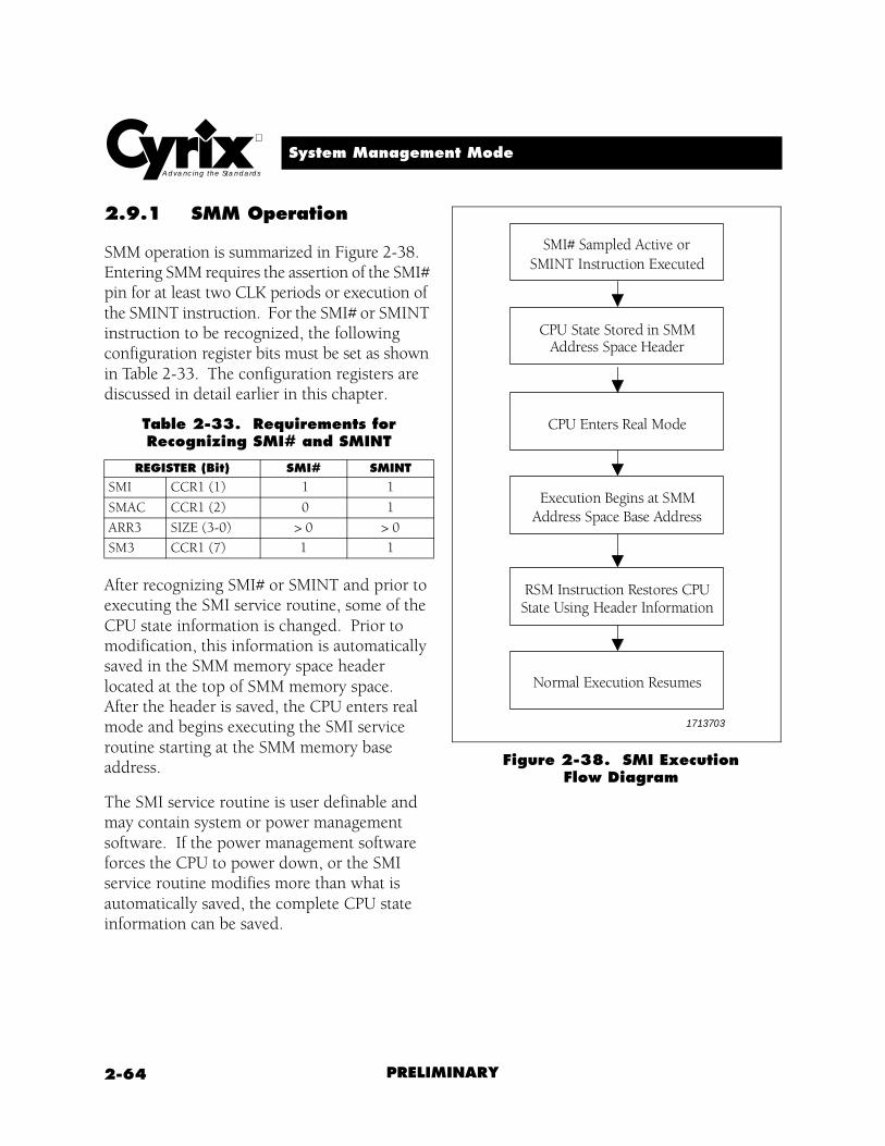
2-64 PRELIMINARY
System Management ModeAdvancing the Standards
1713703
SMI# Sampled Active or
CPU State Stored in SMM
CPU Enters Real Mode
Execution Begins at SMM
RSM Instruction Restores CPU
Normal Execution Resumes
Address Space Header
Address Space Base Address
State Using Header Information
SMINT Instruction Executed
2.9.1 SMM Operation
SMM operation is summarized in Figure 2-38. Entering SMM requires the assertion of the SMI#pin for at least two CLK periods or execution of the SMINT instruction. For the SMI# or SMINT instruction to be recognized, the following configuration register bits must be set as shown in Table 2-33. The configuration registers are discussed in detail earlier in this chapter.
After recognizing SMI# or SMINT and prior to executing the SMI service routine, some of the CPU state information is changed. Prior to modification, this information is automatically saved in the SMM memory space header located at the top of SMM memory space. After the header is saved, the CPU enters real mode and begins executing the SMI service routine starting at the SMM memory base address.
The SMI service routine is user definable and may contain system or power management software. If the power management software forces the CPU to power down, or the SMI service routine modifies more than what is automatically saved, the complete CPU state information can be saved.
Table 2-33. Requirements for Recognizing SMI# and SMINT
REGISTER (Bit) SMI# SMINT
SMI CCR1 (1) 1 1
SMAC CCR1 (2) 0 1
ARR3 SIZE (3-0) > 0 > 0
SM3 CCR1 (7) 1 1
Figure 2-38. SMI ExecutionFlow Diagram

2-65
2
PRELIMINARY
System Management Mode
2.9.2 SMM Memory SpaceHeader
With every SMI interrupt or SMINT instruction, certain CPU state information is automatically saved in the SMM memory space header located at the top of SMM address space as shown
Figure 2-39 and Table 2-34 (Page 2-66). The header contains CPU state information that is modified when servicing an SMI interrupt. In-cluded in this information are two pointers. The Current IP points to the instruction that was ex-ecuting when the SMI was detected.
Figure 2-39. SMM Memory Space Header
DR7
EFLAGS
CR0
031Top of SMM
-4h
-8h
-Ch
-10h
-14h
-18h
-1Ch
-20h
-24h
-28h
P
Current IP
Next IP
CS Selector
CS Descriptor (Bits 63-32)
CS Descriptor (Bits 31-0)
ESI or EDI
I
1713504
31 16 15 0
31 2 1 0
-2Ch
-30h
Address Space
3
S
I/O Write AddressI/O Write Data Size
I/O Write Data
16 15
2122
CPL
H
4
Reserved
Reserved
Reserved
Reserved

2-66 PRELIMINARY
System Management ModeAdvancing the Standards
The Next IP points to the instruction that will be executed after exiting SMM. Also saved are the contents of debug register 7 (DR7), the extended flags register (EFLAGS), and control register 0 (CR0). If SMM has been entered due to an I/O trap for a REP INSx or REP OUTSx instruction, the Current IP and Next IP fields contain the same addresses and the I and P field contain valid information.
If entry into SMM was caused by an I/O trap it is useful for the programmer to know the port address, data size and data value associated with that I/O operation. This information is also saved in the header and is only valid for an I/O write operation. The I/O write information is not restored within the CPU when executing a RSM instruction.
Table 2-34. SMM Memory Space Header
NAME DESCRIPTION SIZE
DR7 The contents of Debug Register 7. 4 Bytes
EFLAGS The contents of Extended Flags Register. 4 Bytes
CR0 The contents of Control Register 0. 4 Bytes
Current IP The address of the instruction executed prior to servicing SMI interrupt. 4 Bytes
Next IP The address of the next instruction that will be executed after exiting SMM mode. 4 Bytes
CS Selector Code segment register selector for the current code segment. 2 Bytes
CPL Current privilege level for current code segment. 2 Bits
CS Descriptor Code segment register descriptor for the current code segment. 8 Bytes
H If set indicates the processor was in a halt or shutdown prior to servicing the SMM interrupt.
1 Bit
S Software SMM Entry Indicator.S = 1, if current SMM is the result of an SMINT instruction.S = 0, if current SMM is not the result of an SMINT instruction.
1 Bit
P REP INSx/OUTSx Indicator.P = 1 if current instruction has a REP prefix.P = 0 if current instruction does not have a REP prefix.
1 Bit
I IN, INSx, OUT, or OUTSx Indicator.I = 1 if current instruction performed is an I/O WRITE.I = 0 if current instruction performed is an I/O READ.
1 Bit
I/O Write Data Size Indicates size of data for the trapped I/O write. 01h = byte 03h = word 0Fh = dword
2 Bytes
I/O Write Address Processor port used for the trapped I/O write. 2 Bytes
I/O Write Data Data associated with the trapped I/O write. 4 Bytes
ESI or EDI Restored ESI or EDI value. Used when it is necessary to repeat a REP OUTSx orREP INSx instruction when one of the I/O cycles caused an SMI# trap.
4 Bytes
Note: INSx = INS, INSB, INSW or INSD instruction.Note: OUTSx = OUTS, OUTSB, OUTSW and OUTSD instruction.
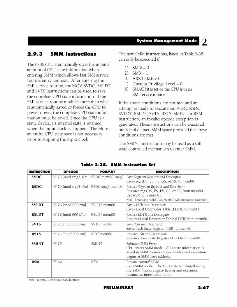
2-67
2
PRELIMINARY
System Management Mode
2.9.3 SMM Instructions
The 6x86 CPU automatically saves the minimalamount of CPU state information when entering SMM which allows fast SMI service routine entry and exit. After entering the SMI service routine, the MOV, SVDC, SVLDT and SVTS instructions can be used to save the complete CPU state information. If the SMI service routine modifies more than what is automatically saved or forces the CPU to power down, the complete CPU state infor-mation must be saved. Since the CPU is a static device, its internal state is retained when the input clock is stopped. Therefore, an entire CPU state save is not necessary prior to stopping the input clock.
The new SMM instructions, listed in Table 2-35, can only be executed if:
1) SMI# = 0 2) SM3 = 1 3) ARR3 SIZE > 0 4) Current Privilege Level = 05) SMAC bit is set or the CPU is in an
SMI service routine.
If the above conditions are not met and an attempt is made to execute an SVDC, RSDC, SVLDT, RSLDT, SVTS, RSTS, SMINT or RSM instruction, an invalid opcode exception is generated. These instructions can be executed outside of defined SMM space provided the aboveconditions are met.
The SMINT instruction may be used as a soft-ware controlled mechanism to enter SMM.
Table 2-35. SMM Instruction Set
INSTRUCTION OPCODE FORMAT DESCRIPTION
SVDC 0F 78 [mod sreg3 r/m] SVDC mem80, sreg3 Save Segment Register and DescriptorSaves reg (DS, ES, FS, GS, or SS) to mem80.
RSDC 0F 79 [mod sreg3 r/m] RSDC sreg3, mem80 Restore Segment Register and DescriptorRestores reg (DS, ES, FS, GS, or SS) from mem80. Use RSM to restore CS. Note: Processing “RSDC CS, Mem80” will produce an exception.
SVLDT 0F 7A [mod 000 r/m] SVLDT mem80 Save LDTR and DescriptorSaves Local Descriptor Table (LDTR) to mem80.
RSLDT 0F 7B [mod 000 r/m] RSLDT mem80 Restore LDTR and DescriptorRestores Local Descriptor Table (LDTR) from mem80.
SVTS 0F 7C [mod 000 r/m] SVTS mem80 Save TSR and DescriptorSaves Task State Register (TSR) to mem80.
RSTS 0F 7D [mod 000 r/m] RSTS mem80 Restore TSR and DescriptorRestores Task State Register (TSR) from mem80.
SMINT 0F 7E SMINT Software SMM EntryCPU enters SMM mode. CPU state information is saved in SMM memory space header and execution begins at SMM base address.
RSM 0F AA RSM Resume Normal ModeExits SMM mode. The CPU state is restored using the SMM memory space header and execution resumes at interrupted point.
Note: mem80 = 80-bit memory location
2-68 PRELIMINARY
System Management ModeAdvancing the Standards
All of the SMM instructions (except RSM andSMINT) save or restore 80 bits of data, allowingthe saved values to include the hidden portionof the register contents.
2.9.4 SMM Memory Space
SMM memory space is defined by setting the SM3 bit and specifying the base address and size of the SMM memory space in the ARR3 register. The base address must be a multiple of the SMM memory space size. For example, a 32 KByte SMM memory space must be located at a 32 KByte address boundary. The memory space size can range from 4 KBytes to 4 GBytes.
SMM memory space accesses are always non-cacheable. SMM accesses ignore the state of the A20M# input pin and drive the A20 address bit to the unmasked value.
SMM memory space can be accessed while in normal mode by setting the SMAC bit in the CCR1 register. This feature may be used to initialize the SMM memory space.
2.9.5 SMI Service RoutineExecution
Upon entry into SMM, after the SMM header has been saved, the CR0, EFLAGS, and DR7 registers are set to their reset values. The Code Segment (CS) register is loaded with the base, as defined by the ARR3 register, and a limit of 4 GBytes. The SMI service routine then begins execution at the SMM base address in real mode.
The programmer must save the value of any registers that may be changed by the SMI service routine. For data accesses immediately after entering the SMI service routine, the programmer must use CS as a segment override. I/O port access is possible during the routine but care must be taken to save registers modified by the I/O instructions. Before using a segment register, the register and the register’s descriptor cache contentsshould be saved using the SVDC instruction. While executing in the SMM space, execution flow can transfer to normal memory locations.
Hardware interrupts, (INTRs and NMIs), may be serviced during a SMI service routine. If interrupts are to be serviced while executing in the SMM memory space, the SMM memory space must be within the 0 to 1 MByte address range to guarantee proper return to the SMI service routine after handling the interrupt.
INTRs are automatically disabled when enteringSMM since the IF flag is set to its reset value. Once in SMM, the INTR can be enabled by setting the IF flag. NMI is also automatically disable when entering SMM. Once in SMM, NMI can be enabled by setting NMI_EN in CCR3. If NMI is not enabled, the CPU latches one NMI event and services the interrupt after NMI has been enabled or after exiting SMM through the RSM instruction.
Within the SMI service routine, protected modemay be entered and exited as required, and realor protected mode device drivers may be called.

2-69
2
PRELIMINARY
Shutdown and Halt
To exit the SMI service routine, a Resume (RSM) instruction, rather than an IRET, is executed. The RSM instruction causes the 6x86 processor to restore the CPU state using the SMM header information and resume execution at the interrupted point. If the full CPU state was saved by the programmer, the stored values should be reloaded prior to executing the RSM instruction using the MOV, RSDC, RSLDT and RSTS instructions.
CPU States Related to SMM and Suspend Mode
The state diagram shown in Figure 2-40 (Page 2-70) illustrates the various CPU states associ-ated with SMM and suspend mode. While in the SMI service routine, the 6x86 CPU can enter suspend mode either by (1) executing a halt (HLT) instruction or (2) by asserting the SUSP# input.
During SMM operations and while in SUSP# initiated suspend mode, an occurrence of SMI#, NMI, or INTR is latched. (In order for INTR to be latched, the IF flag must be set.) The INTR or NMI is serviced after exiting suspend mode.
If suspend mode is entered via a HLT instruc-tion from the operating system or application software, the reception of an SMI# interrupt causes the CPU to exit suspend mode and enter SMM.
2.10 Shutdown and Halt
The Halt Instruction (HLT) stops program ex-ecution and prevents the processor from usingthe local bus until restarted. The 6x86 CPUthen issues a special Stop Grant bus cycle and enters a low-power suspend mode if the SUSP_HLT bit in CCR2 is set. SMI, NMI, INTR with interrupts enabled (IF bit in EFLAGS=1), WM_RST or RESET forces the CPU out of the halt state. If interrupted, the saved code seg-ment and instruction pointer specify the in-struction following the HLT.
Shutdown occurs when a severe error is detectedthat prevents further processing. An NMI inputcan bring the processor out of shutdown if the IDT limit is large enough to contain the NMI interrupt vector and the stack has enough room to contain the vector and flag informa-tion. Otherwise, shutdown can only be exited by a processor reset.

2-70 PRELIMINARY
Shutdown and HaltAdvancing the Standards
Figure 2-40. SMM and Suspend Mode State Diagram
OS/Application
SoftwareRESET
RSM*SMI#=0
HLT*
SUSP#=1
NMI or INTR
SUSP#=0
SUSP#=1
HLT*
INTR or NMIIRET*
INTR and NMI
IRET*
IRET*
* Instructions
SMI# = 0
(INTR, NMI and SMI latched)
(INTR and NMI latched)
SMI Service
1715903
Suspend Mode Interrupt Service
Suspend Mode
Suspend Mode
Suspend Mode
SUSP#=0
Non-SMM Operations
SMM Operations
(SUSPA# = 0) Routine
(SUSPA# = 0)
(SUSPA# = 0)
Routine(SMI#=0)
(SUSPA# = 0)
Interrupt ServiceRoutine
Interrupt ServiceRoutine
SMINT*
NMI or INTR
2-71
2
PRELIMINARY
Protection
2.11 Protection
Segment protection and page protection are safeguards built into the 6x86 CPU protected mode architecture which deny unauthorized or incorrect access to selected memory addresses. These safeguards allow multi-tasking programs to be isolated from each other and from the operating system. Page protection is discussed earlier in this chapter. This section concentrates on segment protec-tion.
Selectors and descriptors are the key elements in the segment protection mechanism. The segment base address, size, and privilege level are established by a segment descriptor. Privi-lege levels control the use of privileged instruc-tions, I/O instructions and access to segments and segment descriptors. Selectors are used to locate segment descriptors.
Segment accesses are divided into two basic types, those involving code segments (e.g., control transfers) and those involving data accesses. The ability of a task to access a segment depends on the:
• segment type• instruction requesting access• type of descriptor used to define the
segment• associated privilege levels (described
below).
Data stored in a segment can be accessed only by code executing at the same or a more privi-leged level. A code segment or procedure can only be called by a task executing at the same or a less privileged level.
2.11.1 Privilege Levels
The values for privilege levels range between 0 and 3. Level 0 is the highest privilege level (most privileged), and level 3 is the lowest privilege level (least privileged). The privilege level in real mode is effectively 0.
The Descriptor Privilege Level (DPL) is the privilege level defined for a segment in the segment descriptor. The DPL field specifies the minimum privilege level needed to access the memory segment pointed to by the descriptor.
The Current Privilege Level (CPL) is defined as the current task’s privilege level. The CPL of an executing task is stored in the hidden portion of the code segment register and essen-tially is the DPL for the current code segment.
The Requested Privilege Level (RPL) speci-fies a selector’s privilege level and is used to distinguish between the privilege level of a routineactually accessing memory (the CPL), and the privilege level of the original requestor (the RPL)of the memory access. The lesser of the RPL and CPL is called the effective privilege level (EPL). Therefore, if RPL = 0 in a segment selector, the effective privilege level is always determined by the CPL. If RPL = 3, the effective privilege level is always 3 regardless of the CPL.
For a memory access to succeed, the effective privilege level (EPL) must be at least as privi-leged as the descriptor privilege level (EPL ≤DPL). If the EPL is less privileged than the DPL (EPL > DPL), a general protection fault is generated. For example, if a segment has a DPL = 2, an instruction accessing the segment only succeeds if executed with an EPL ≤ 2.

2-72 PRELIMINARY
ProtectionAdvancing the Standards
2.11.2 I/O Privilege Levels
The I/O Privilege Level (IOPL) allows the oper-ating system executing at CPL=0 to define the least privileged level at which IOPL-sensitive instructions can unconditionally be used. The IOPL-sensitive instructions include CLI, IN, OUT, INS, OUTS, REP INS, REP OUTS, and STI. Modification of the IF bit in the EFLAGS register is also sensitive to the I/O privilege level. The IOPL is stored in the EFLAGS register.
An I/O permission bit map is available as defined by the 32-bit Task State Segment (TSS). Since each task can have its own TSS, access to individual processor I/O ports can be granted through separate I/O permission bit maps.
If CPL ≤ IOPL, IOPL-sensitive operations can be performed. If CPL > IOPL, a general protection fault is generated if the current task is associated with a 16-bit TSS. If the current task is associated with a 32-bit TSS and CPL > IOPL, the CPU consults the I/O permission bitmap in the TSS to determine on a port-by-portbasis whether or not I/O instructions (IN, OUT, INS, OUTS, REP INS, REP OUTS) are permitted, and the remaining IOPL-sensitive operations generate a general protection fault.
2.11.3 Privilege Level Transfers
A task’s CPL can be changed only through intersegment control transfers using gates or task switches to a code segment with a different privilege level. Control transfers result from exception and interrupt servicing and from execution of the CALL, JMP, INT, IRET and RET instructions.
There are five types of control transfers that are summarized in Table 2-36 (Page 2-73). Controltransfers can be made only when the operation causing the control transfer references the correctdescriptor type. Any violation of these descriptorusage rules causes a general protection fault.
Any control transfer that changes the CPL within a task results in a change of stack. The initial values for the stack segment (SS) and stack pointer (ESP) for privilege levels 0, 1, and 2 are stored in the TSS. During a CALL control transfer, the SS and ESP are loaded with the new stack pointer and the previous stack pointer is saved on the new stack. When returning to the original privilege level, the RET or IRET instruction restores the less-privi-leged stack.

2-73
2
PRELIMINARY
Protection
Table 2-36. Descriptor Types Used for Control Transfer
TYPE OF CONTROL TRANSFEROPERATION
TYPESDESCRIPTORREFERENCED
DESCRIPTORTABLE
Intersegment within the same privilege level. JMP, CALL, RET, IRET* Code Segment GDT or LDT
Intersegment to the same or a more privileged level.Interrupt within task (could change CPL level).
CALL Gate Call GDT or LDT
Interrupt Instruction, Exception, ExternalInterrupt
Trap or Interrupt Gate IDT
Intersegment to a less privileged level (changes task CPL).
RET, IRET* Code Segment GDT or LDT
Task Switch via TSS CALL, JMP Task State Segment GDT
Task Switch via Task Gate CALL, JMP Task Gate GDT or LDT
IRET**, Interrupt Instruction, Exception, External Interrupt
Task Gate IDT
* NT (Nested Task bit in EFLAGS) = 0** NT (Nested Task bit in EFLAGS) = 1
Gates
Gate descriptors provide protection for privi-lege transfers among executable segments. Gatesare used to transition to routines of the same or a more privileged level. Call gates, interrupt gates and trap gates are used for privilege transferswithin a task. Task gates are used to transfer between tasks.
Gates conform to the standard rules of privi-lege. In other words, gates can be accessed by a task if the effective privilege level (EPL) is the same or more privileged than the gate descrip-tor’s privilege level (DPL).
2.11.4 Initialization andTransition to ProtectedMode
The 6x86 microprocessor switches to real mode immediately after RESET. While operating in real mode, the system tables and registers should be initialized. The GDTR and IDTR must point to a valid GDT and IDT, respectively. The GDT must contain descriptors which describe the initial code and data segments.
The processor can be placed in protected mode by setting the PE bit in the CR0 register. After enabling protected mode, the CS register shouldbe loaded and the instruction decode queue should be flushed by executing an intersegmentJMP. Finally, all data segment registers should be initialized with appropriate selector values.
2-74 PRELIMINARY
Virtual 8086 ModeAdvancing the Standards
2.12 Virtual 8086 Mode
Both real mode and virtual 8086 (V86) mode are supported by the 6x86 CPU allowing execu-tion of 8086 application programs and 8086 operating systems. V86 mode allows the execution of 8086-type applications, yet still permits use of the 6x86 CPU paging mecha-nism. V86 tasks run at privilege level 3. When loaded, all segment limits are set to FFFFh (64K) as in real mode.
2.12.1 V86 MemoryAddressing
While in V86 mode, segment registers are used in an identical fashion to real mode. The contents of the segment register are multiplied by 16 and added to the offset to form the segment base linear address. The 6x86 CPU permits the operating system to select which programs use the V86 address mechanism and which programs use protected mode addressing for each task.
The 6x86 CPU also permits the use of paging when operating in V86 mode. Using paging, the 1-MByte address space of the V86 task can be mapped to anywhere in the 4-GByte linear address space of the 6x86 CPU.
The paging hardware allows multiple V86 tasks to run concurrently, and provides protec-tion and operating system isolation. The paging hardware must be enabled to run multiple V86 tasks or to relocate the address space of a V86 task to physical address space greater than 1 MByte.
2.12.2 V86 Protection
All V86 tasks operate with the least amount of privilege (level 3) and are subject to all of the 6x86 CPU protected mode protection checks. As a result, any attempt to execute a privileged instruction within a V86 task results in a general protection fault.
In V86 mode, a slightly different set of instruc-tions are sensitive to the I/O privilege level (IOPL) than in protected mode. These instruc-tions are: CLI, INT n, IRET, POPF, PUSHF, and STI. The INT3, INTO and BOUND variations of the INT instruction are not IOPL sensitive.
2.12.3 V86 Interrupt Handling
To fully support the emulation of an 8086-type machine, interrupts in V86 mode are handled as follows. When an interrupt or exception is serviced in V86 mode, program execution transfers to the interrupt service routine at privilege level 0 (i.e., transition from V86 to protected mode occurs) and the VM bit in the EFLAGS register is cleared. The protected mode interrupt service routine then deter-mines if the interrupt came from a protected mode or V86 application by examining the VM bit in the EFLAGS image stored on the stack. The interrupt service routine may then choose to allow the 8086 operating system to handle the interrupt or may emulate the function of the interrupt handler. Following completion of the interrupt service routine, an IRET instruction restores the EFLAGS register (restores VM=1) and segment selectors and control returns to the interrupted V86 task.
2-75
2
PRELIMINARY
Floating Point Unit Operations
2.12.4 Entering and LeavingV86 Mode
V86 mode is entered from protected mode by either executing an IRET instruction at CPL = 0 or by task switching. If an IRET is used, the stack must contain an EFLAGS image with VM = 1. If a task switch is used, the TSS must contain an EFLAGS image containing a 1 in the VM bit position. The POPF instruction cannot be used to enter V86 mode since the state of the VM bit is not affected. V86 mode can only be exited as the result of an interrupt or exception. The transition out must use a 32-bit trap or interrupt gate which must point to a non-conforming privilege level 0 segment (DPL = 0), or a 32-bit TSS. These restrictions are required to permit the trap handler to IRET back to the V86 program.
2.13 Floating Point UnitOperations
The 6x86 CPU includes an on-chip FPU that provides the user access to a complete set of floating point instructions (see Chapter 6). Information is passed to and from the FPU using eight data registers accessed in a stack-like manner, a control register, and a status register. The 6x86 CPU also provides a data register tag word which improves context switching and performance by maintaining empty/non-empty status for each of the eight data registers. In addition, registers in the CPU contain pointers to (a) the memory loca-tion containing the current instruction word and (b) the memory location containing the operand associated with the current instruc-tion word (if any).
FPU Tag Word Register. The 6x86 CPU maintains a tag word register (Figure 2-41 (Page 2-76)) comprised of two bits for each physical data register. Tag Word fields assume one of four values depending on the contents of their associated data registers, Valid (00), Zero (01), Special (10), and Empty (11). Note: Denormal, Infinity, QNaN, SNaN and unsupported formats are tagged as “Special”. Tag values are maintained transparently by the 6x86 CPU and are only available to the pro-grammer indirectly through the FSTENV and FSAVE instructions.
FPU Control and Status Registers. The FPU circuitry communicates information about its status and the results of operations to the programmer via the status register. The FPU status register is comprised of bit fields that reflect exception status, operation execu-tion status, register status, operand class, and comparison results. The FPU status register bit definitions are shown in Figure 2-42 (Page 2-76) and Table 2-37 (Page 2-76).
The FPU Mode Control Register (MCR) is used by the CPU to specify the operating mode of the FPU. The MCR contains bit fields which specify the rounding mode to be used, the pre-cision by which to calculate results, and the exception conditions which should be report-ed to the CPU via traps. The user controls pre-cision, rounding, and exception reporting by setting or clearing appropriate bits in the MCR. The FPU mode control register bit def-initions are shown in Figure 2-43 (Page 2-77)and Table 2-38 (Page 2-77).

2-76 PRELIMINARY
Floating Point Unit OperationsAdvancing the Standards
15 14 13 12 11 10 9 8 7 6 5 4 3 2 1 0
Tag(7) Tag(6) Tag(5) Tag(4) Tag(3) Tag(2) Tag(1) Tag(0)
Figure 2-41. FPU Tag Word Register
15 12 11 8 7 4 3 0
B C3 S S S C2 C1 C0 ES SF P U O Z D I
Figure 2-42. FPU Status Register
Table 2-37. FPU Status Register Bit Definitions
BITPOSITION NAME DESCRIPTION
15 B Copy of the ES bit. (ES is bit 7 in this table.)
14, 10 - 8 C3 - C0 Condition code bits.
13 - 11 SSS Top of stack register number which points to the current TOS.
7 ES Error indicator. Set to 1 if an unmasked exception is detected.
6 SF Stack Fault or invalid register operation bit.
5 P Precision error exception bit.
4 U Underflow error exception bit.
3 O Overflow error exception bit.
2 Z Divide by zero exception bit.
1 D Denormalized operand error exception bit.
0 I Invalid operation exception bit.
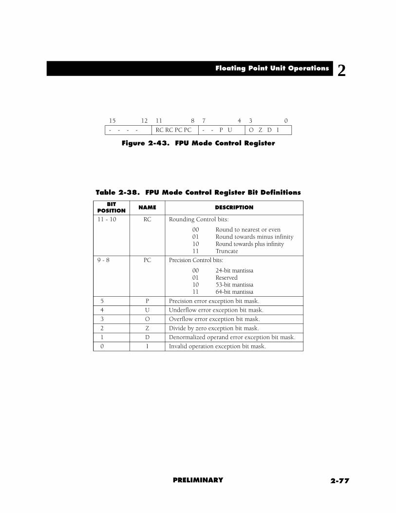
2-77
2
PRELIMINARY
Floating Point Unit Operations
15 12 11 8 7 4 3 0
- - - - RC RC PC PC - - P U O Z D I
Figure 2-43. FPU Mode Control Register
Table 2-38. FPU Mode Control Register Bit Definitions
BITPOSITION
NAME DESCRIPTION
11 - 10 RC Rounding Control bits:
00 Round to nearest or even01 Round towards minus infinity10 Round towards plus infinity11 Truncate
9 - 8 PC Precision Control bits:
00 24-bit mantissa01 Reserved10 53-bit mantissa11 64-bit mantissa
5 P Precision error exception bit mask.
4 U Underflow error exception bit mask.
3 O Overflow error exception bit mask.
2 Z Divide by zero exception bit mask.
1 D Denormalized operand error exception bit mask.
0 I Invalid operation exception bit mask.

Related Documents