03/27/22 ECE331 (KEH) 1 ECE331 Lab 4 Introduction Interrupt Processing Read Huang Text Ch. 6

6/17/2015ECE331 (KEH)1 ECE331 Lab 4 Introduction Interrupt Processing Read Huang Text Ch. 6.
Dec 20, 2015
Welcome message from author
This document is posted to help you gain knowledge. Please leave a comment to let me know what you think about it! Share it to your friends and learn new things together.
Transcript

04/18/23 ECE331 (KEH) 1
ECE331 Lab 4 Introduction
Interrupt Processing
Read Huang Text Ch. 6
04/18/23 ECE331 (KEH) 2
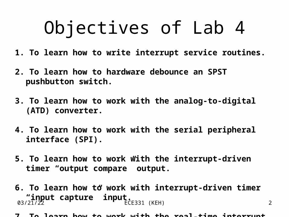
Objectives of Lab 41. To learn how to write interrupt service routines.
2. To learn how to hardware debounce an SPST pushbutton switch.
3. To learn how to work with the analog-to-digital (ATD) converter.
4. To learn how to work with the serial peripheral interface (SPI).
5. To learn how to work with the interrupt-driven timer “output compare” output.
6. To learn how to work with interrupt-driven timer “input capture” input.
7. To learn how to work with the real-time interrupt (RTI) mechanism.

04/18/23 ECE331 (KEH) 3
DeliverablesTwo memo-style lab reports must be submitted:
Lab Report 4A is due at the beginning of the second week of lab, and it must report on the combination lock and the instrument tuner application.
Lab Report 4B is due one week later, and it must report on the DVM application, and all four interrupt-driven applications in addition to the main program LED blinking application must be demonstrated to run “simultaneously” at this time.
Both lab reports must include and refer to the following attachments:(1) schematic diagrams (drafted using ORCAD) of all interfacing hardware (2) flow chart (3) commented assembly source code(4) description of testing procedures and test results

04/18/23 ECE331 (KEH) 4
The 9S12’s hardware interrupt mechanism will be used in this lab to implement four foreground tasks, each of which is written as a separate interrupt service routine, while a simple (non-interrupt driven) LED-blinking program will run as a main program in the background.
The key thing to remember is that each interrupt service routine (ISR) must be structured so that it executes very quickly (within only a few microseconds). Then the interrupt service routine must return to the main program (background) task, as soon as possible, so that the background task has a chance to run, and so that other interrupts can be serviced as they occur, in a timely (“real time”) fashion. This is important, because while an interrupt service routine is executed, the 9S12’s CPU disables (masks out) other I-related interrupts by setting the condition code register’s I (IRQ Mask) bit to 1, thereby locking out other pending interrupts, making them wait until the currently executing interrupt routine is finished. We do not want other pending interrupt request to go without being serviced for too long.
04/18/23 ECE331 (KEH) 5
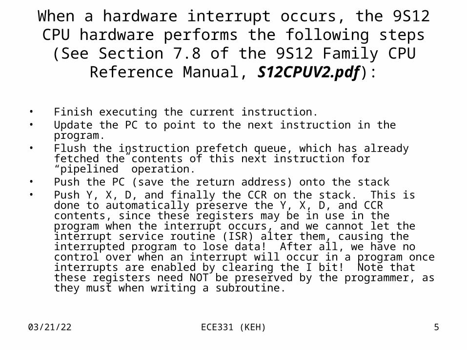
When a hardware interrupt occurs, the 9S12 CPU hardware performs the following steps (See Section 7.8 of the 9S12 Family CPU Reference Manual, S12CPUV2.pdf):
• Finish executing the current instruction. • Update the PC to point to the next instruction in the program. • Flush the instruction prefetch queue, which has already fetched
the contents of this next instruction for “pipelined” operation. • Push the PC (save the return address) onto the stack • Push Y, X, D, and finally the CCR on the stack. This is done to
automatically preserve the Y, X, D, and CCR contents, since these registers may be in use in the program when the interrupt occurs, and we cannot let the interrupt service routine (ISR) alter them, causing the interrupted program to lose data! After all, we have no control over when an interrupt will occur in a program once interrupts are enabled by clearing the I bit! Note that these registers need NOT be preserved by the programmer, as they must when writing a subroutine.

04/18/23 ECE331 (KEH) 6
• The CCR’s I bit (IRQ Mask bit) is then set to 1 by the 9S12’s CPU interrupt processing hardware in order to mask out any further I-bit related interrupts from disrupting the interrupt service routine.
• Set X bit if an XIRQ routine is pending (to disable further XIRQ-related interrupts while this one is being processed.)
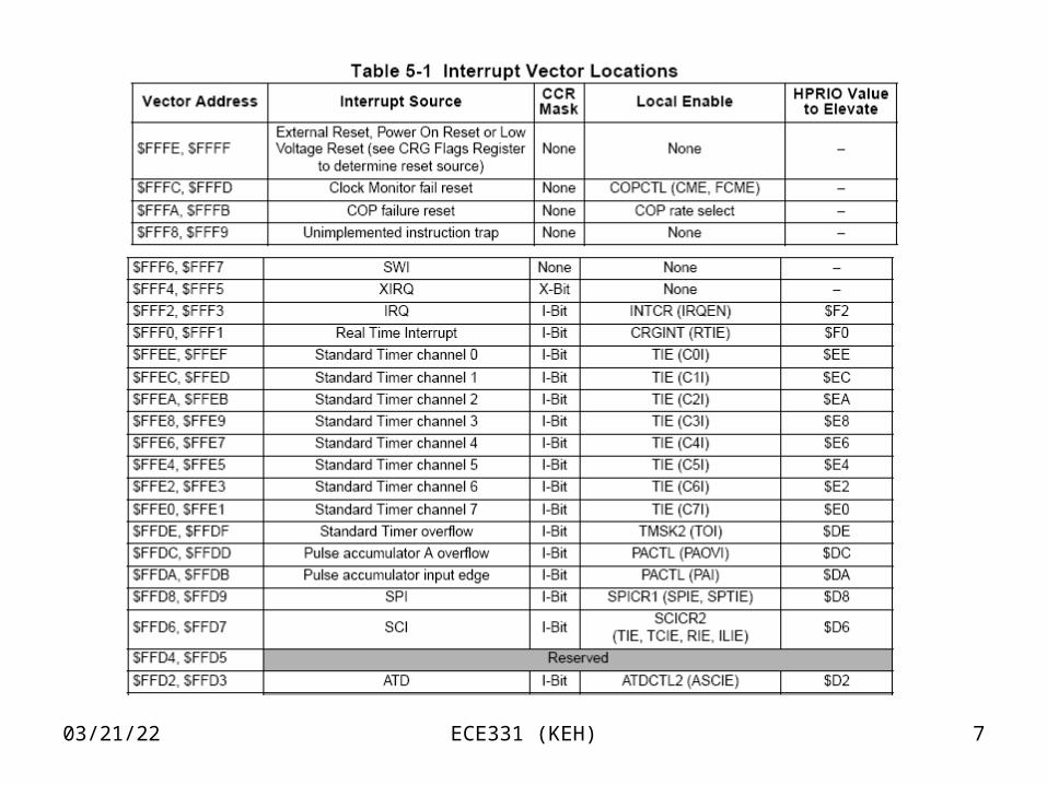
• Load contents of interrupt vector into PC for the highest-priority request that was pending at the beginning of the interrupt sequence. See Table 5-1 of the MC9S12 Family Device User Guide, 9S12C128DGV1.pdf, for the interrupt vector addresses and also the prioritization of the interrupts, and whether they are X-bit related or I-bit related, etc.
• The 9S12 begins executing the interrupt service routine (ISR) at the location pointed to by this interrupt vector.
• At the end of the ISR, a “Return From Interrupt service routine” (RTI) instruction will unstack CCR, D, X, Y, and finally unstack the PC, thereby restoring the I bit and X bit to their original state before the interrupt occurs (re-enabling I-bit and possibly X-bit related interrupts, since the present interrupt service routine has now finished), restore the CPU registers to their pre-interrupt values, and allow the interrupted program to resume where it left off!
04/18/23 ECE331 (KEH) 7
04/18/23 ECE331 (KEH) 8
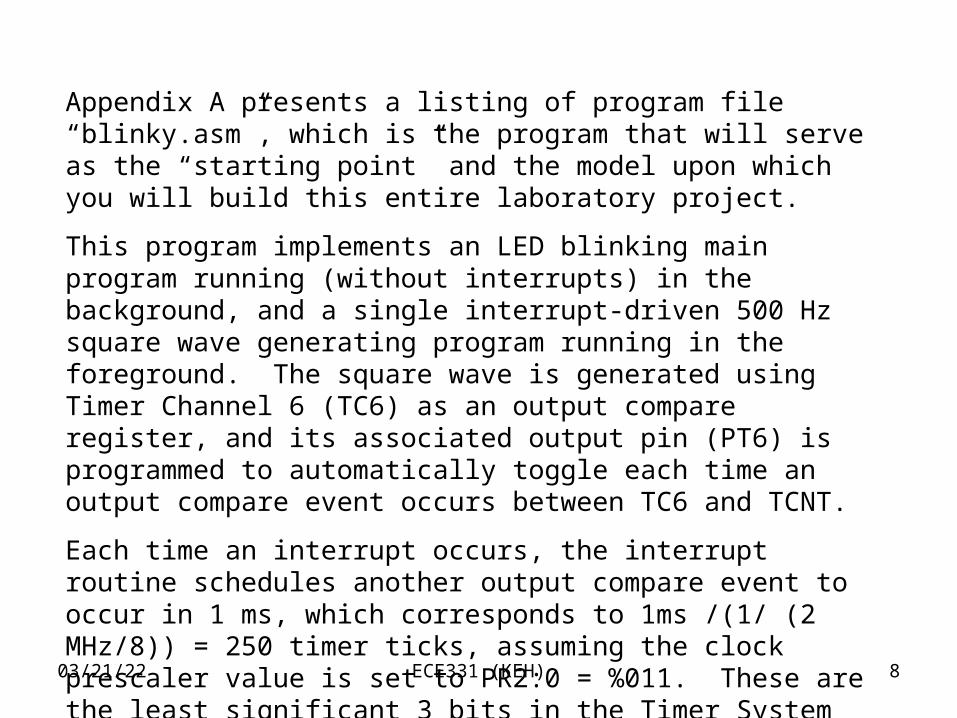
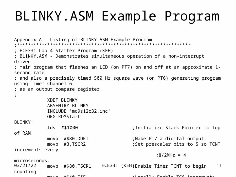
Appendix A presents a listing of program file “blinky.asm”, which is the program that will serve as the “starting point” and the model upon which you will build this entire laboratory project.
This program implements an LED blinking main program running (without interrupts) in the background, and a single interrupt-driven 500 Hz square wave generating program running in the foreground. The square wave is generated using Timer Channel 6 (TC6) as an output compare register, and its associated output pin (PT6) is programmed to automatically toggle each time an output compare event occurs between TC6 and TCNT.
Each time an interrupt occurs, the interrupt routine schedules another output compare event to occur in 1 ms, which corresponds to 1ms /(1/ (2 MHz/8)) = 250 timer ticks, assuming the clock prescaler value is set to PR2:0 = %011. These are the least significant 3 bits in the Timer System Control Register 2 (TSCR2). (See Section 3.3.11 in the TIM16B8C Timer Block Guide, S12TIM16B8CV1.pdf.

04/18/23 ECE331 (KEH) 9
Initialization tasks performed by the main program• Initialize the Timer Channel 6 (TC6) interrupt vector to point to the starting address of the
Timer Output Compare 6 interrupt service routine (TOC6ISR). This is done on our 9S12C32 modules in the same way the RESET vector is initialized using the ORG assembler directive followed by the “form double byte” (FDB) directive to load the appropriate pair of memory locations that correspond to the Timer Channel 6 interrupt vector, $FFE2:$FFE3 (See Section 5.2.1 of the MC9S12C Family Device User Guide, 9S12C128DGV1.pdf), with the starting address of the user-written TOC6ISR.
• Set the prescale bits PR2:0 = %011 in the least significant 3 bits of the TSCR2 register (divide 2 MHz bus clock by 8, yielding a 4 us timer tick period.
• Set the Timer Enable (TEN) bit (Bit 7 of TSCR1) as done in the previous lab.• Locally enable TC6 interrupts by setting Bit 6 of the timer interrupt enable (TIE) register; recall
timer channel interrupts were disabled in the previous lab, but in this lab we are enabling them.
• Configure TC6 to be an output compare (as opposed to an input capture) register, by setting to 1 the appropriate bit (Bit 6) in the Timer Input Capture/ Output Compare Select Register (TIOS).
• Write the appropriate data to the Timer Control Register 1 (TCTL1) to configure Pin PT6 to toggle when the output compare event occurs (See Section 3.3.8 of the TIM16B8C Timer Block Guide.)
• Add TCNT to N = 1 ms / (2 MHz / 8) = 250, then write the result (TCNT + N) to the output compare register TC6, thereby scheduling an output compare interrupt to occur, along with the toggling of Pin PT6, in 1 ms.
• Clear the TC6 flag in the TFLG1 register so that an interrupt will not occur until the first output compare event occurs. Remember, this is done by writing a 1 to Bit 6 of TFLG1. Writing a zero to a flag in TFLG1 does not change the flag at all. Thus “MOVB #$40,TFLG1” will clear the TC6 flag and leave all of the other flags alone, as we desire.
• Finally, globally enable all of the I-bit masked interrupts by clearing the processor’s condition code register’s I bit using the “CLI” instruction.
04/18/23 ECE331 (KEH) 10
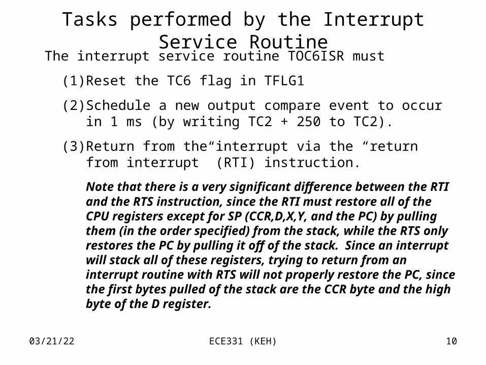
The interrupt service routine TOC6ISR must
(1) Reset the TC6 flag in TFLG1
(2) Schedule a new output compare event to occur in 1 ms (by writing TC2 + 250 to TC2).
(3) Return from the interrupt via the “return from interrupt” (RTI) instruction.
Note that there is a very significant difference between the RTI and the RTS instruction, since the RTI must restore all of the CPU registers except for SP (CCR,D,X,Y, and the PC) by pulling them (in the order specified) from the stack, while the RTS only restores the PC by pulling it off of the stack. Since an interrupt will stack all of these registers, trying to return from an interrupt routine with RTS will not properly restore the PC, since the first bytes pulled of the stack are the CCR byte and the high byte of the D register.
Tasks performed by the Interrupt Service Routine
04/18/23 ECE331 (KEH) 11
Appendix A. Listing of BLINKY.ASM Example Program;***************************************************************; ECE331 Lab 4 Starter Program (KEH); BLINKY.ASM - Demonstrates simultaneous operation of a non-interrupt driven ; main program that flashes an LED (on PT7) on and off at an approximate 1-second rate ; and also a precisely timed 500 Hz square wave (on PT6) generating program using Timer Channel 6 ; as an output compare register.; XDEF BLINKY ABSENTRY BLINKY INCLUDE 'mc9s12c32.inc' ORG ROMStartBLINKY: lds #$1000 ;Initialize Stack Pointer to top of RAM movb #$80,DDRT ;Make PT7 a digital output. movb #3,TSCR2 ;Set prescaler bits to 5 so TCNT increments every ;8/2MHz = 4 microseconds. movb #$80,TSCR1 ;Enable Timer TCNT to begin counting movb #$40,TIE ;Locally Enable TC6 interrupts movb #$40,TIOS ;Make TC6 an Output Compare register movb #$10,TCTL1 ;Make TC6 pin toggle when the scheduled “output
;compare” event occurs.
BLINKY.ASM Example Program
04/18/23 ECE331 (KEH) 12
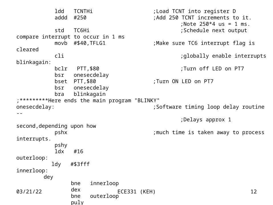
ldd TCNTHi ;Load TCNT into register D addd #250 ;Add 250 TCNT increments to it.
;Note 250*4 us = 1 ms. std TC6Hi ;Schedule next output compare interrupt to occur in 1 ms movb #$40,TFLG1 ;Make sure TC6 interrupt flag is cleared cli ;globally enable interruptsblinkagain: bclr PTT,$80 ;Turn off LED on PT7 bsr onesecdelay bset PTT,$80 ;Turn ON LED on PT7 bsr onesecdelay bra blinkagain;*********Here ends the main program "BLINKY"onesecdelay: ;Software timing loop delay routine -- ;Delays approx 1 second,depending upon how pshx ;much time is taken away to process interrupts. pshy ldx #16outerloop: ldy #$3fffinnerloop:
dey bne innerloop dex bne outerloop puly pulx rts

04/18/23 ECE331 (KEH) 13
TOC6ISR: ldd TC6Hi addd #250 ;Schedule another interrupt in 1 ms after last interrupt std TC6Hi movb #$40,TFLG1 ;Relax the TC6 interrupt flag
;DO NOT DO THIS WITH A ;BSET TFLG1,$40
rti ;**************************************************************;* Initialize Reset Vector and TC6 Interrupt Vector *;************************************************************** ORG $FFFE fdb BLINKY ;Make reset vector point to entry point of BLINKY program ORG $FFE2 fdb TOC6ISR ;Make TC6 interrupt vector point to TC6 interrupt rtn
BLINKY ISR
04/18/23 ECE331 (KEH) 14

04/18/23 ECE331 (KEH) 15
Port T Output Compare Pin Control
04/18/23 ECE331 (KEH) 16
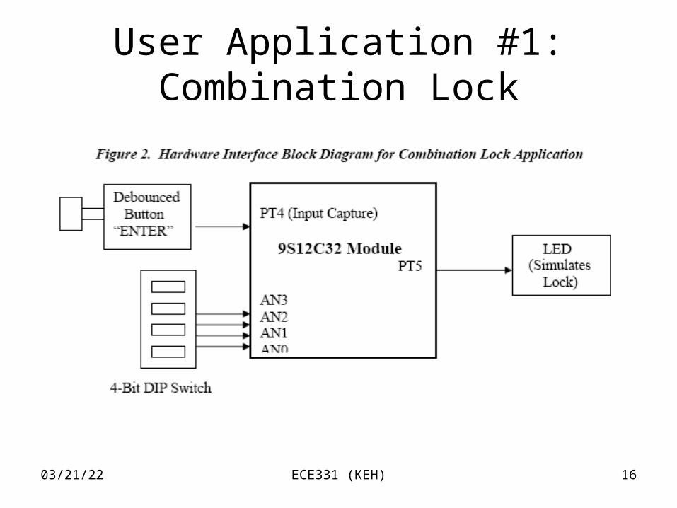
User Application #1: Combination Lock

04/18/23 ECE331 (KEH) 17
Things to add to your main program
• Set up PORT AD so the PTAD3:0 pins are digital inputs with pull-ups turned off by properly setting the ATDDIEN, DDRAD, and the PERAD registers.
• PORT T must be configured so that PT5 is configured as a digital output via the DDRT register.
• Initialize the TC4 interrupt vector. • Configure Pin PT4 as an “input capture” pin by clearing the
appropriate bit in the TIOS register. • Make PT4 falling-edge sensitive by setting the appropriate bits in
the TCTL3 register.• Clear the TC4 interrupt flag in the TFLG1 register.• Locally enable TC4 interrupts (as well as continuing to enable TC6
interrupts needed by the 500 Hz square wave generating routine) using the Timer Interrupt Enable (TIE) register.

04/18/23 ECE331 (KEH) 18

04/18/23 ECE331 (KEH) 19
Port T Input Capture Pin Control
TCTL3 (offset$0A) and TCTL4 (offset $0B) Registers

04/18/23 ECE331 (KEH) 20
TC4 Interrupt Routine

04/18/23 ECE331 (KEH) 21
04/18/23 ECE331 (KEH) 22
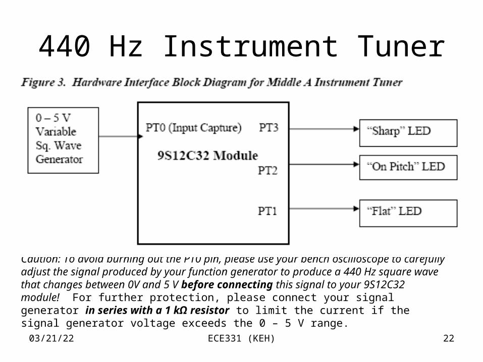
440 Hz Instrument Tuner
Caution: To avoid burning out the PT0 pin, please use your bench oscilloscope to carefully adjust the signal produced by your function generator to produce a 440 Hz square wave that changes between 0V and 5 V before connecting this signal to your 9S12C32 module! For further protection, please connect your signal generator in series with a 1 kΩ resistor to limit the current if the signal generator voltage exceeds the 0 – 5 V range.

04/18/23 ECE331 (KEH) 23
(1)Reset the PT0 interrupt flag. Remember: an interrupt condition needs to be “relaxed” (de-asserted) by its service routine, in order not to cause endless interrupts!
(2) Read the TC0 input capture register contents.
(3) Subtract this value from the (stored) previous TC0 register contents.
(4) Store the present input capture register contents in a (word-sized) RAM location for use when the next TC0 input capture interrupt occurs.
(5) Also, appropriate initialization statements will need to be added to the main program (before the CLI is executed), similar to what was suggested in the previous section.
Tasks for the TC0 Interrupt Routine
04/18/23 ECE331 (KEH) 24
“Similar” Example Program
• This example consists of interrupt routine that turns ON an LED on PM2 if the 0V/5V square wave generator attached to PT2 has a frequency greater than 1 kHz, and turns the LED OFF if the frequency falls below 1 kHz.
• Generator should be adjusted to 0V/5V BEFORE connecting it to PT2.
• Also, the generator should be connected in series with a 1-kilohm resistor to protect module in the event the generator voltage does not vary between 0V/5V

04/18/23 ECE331 (KEH) 25
; export symbols XDEF Entry ABSENTRY Entry ; include derivative specific macros INCLUDE 'mc9s12c128.inc'; variable/data section ORG RAMStartSAVE_TIME: DS.W 1 ;Holds previous TCNT value ORG ROMStartEntry: MOVB #4,DDRM ;Make PM2 an output. MOVB #3,TSCR2 ;Set prescaler bits to %011 => ;TICK_PERIOD= 8/2MHz = 4 microseconds. BSET TSCR1,$80 ;Enable TIMER TCNT to begin counting. MOVB #4,TIE ;Locally enable TC2 interrupts. BCLR TIOS,4 ;Make TC2 an input capture. BSET TCTL4,$10 BCLR TCTL4,$20 ;Make PT2 rising edge sensitive. MOVB #4,TFLG1 ;Clear TC2 interrupt flag. CLI ;Globally enable interrupts. DynHalt: BRA DynHalt
04/18/23 ECE331 (KEH) 26
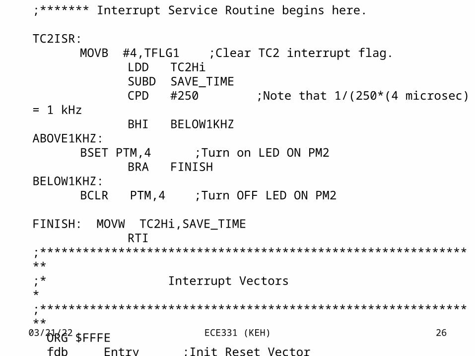
;******* Interrupt Service Routine begins here.
TC2ISR:MOVB #4,TFLG1 ;Clear TC2 interrupt flag.
LDD TC2Hi SUBD SAVE_TIME CPD #250 ;Note that 1/(250*(4 microsec) = 1 kHz BHI BELOW1KHZABOVE1KHZ:
BSET PTM,4 ;Turn on LED ON PM2 BRA FINISH BELOW1KHZ:
BCLR PTM,4 ;Turn OFF LED ON PM2 FINISH: MOVW TC2Hi,SAVE_TIME RTI;**************************************************************
;* Interrupt Vectors *;************************************************************** ORG $FFFE fdb Entry ;Init Reset Vector ORG $FFEA fdb TC2ISR ;Init Timer Channel 2 ISR Vector

04/18/23 ECE331 (KEH) 27
0-5V Digital Voltmeter (DVM)

04/18/23 ECE331 (KEH) 28
DVM Application Involves the following 9S12 On-Chip Resources:
• RTI (Real Time Interrupt) See Section 4.2.6 of the Clock Reset Generator (CRG) User Guide, S12CRGV4.pdf.
• ATD (Analog-to-digital Converter) See Section ATD10B8C Block User Guide, S12ATD10B8CV2.pdf.
• SPI (Serial Peripheral Interface) See SPI Block Guide, S12SPIV3.pdf.

04/18/23 ECE331 (KEH) 29
OE\ -> ground
(to permanently enable tri-state output drivers.)
SRCLR\ -> +5V
( to permanently disable Shift Reg reset signal.)
SRCLK pulsed (L->H) (after data shifted into desired position in shift register in order to clock shift register into output holding register.)
74HC595 Serial-in, Parallel-out, Serial-in (PISO) Shift Register

04/18/23 ECE331 (KEH) 30
Real-Time Interrupt (RTI) Mechanism

04/18/23 ECE331 (KEH) 31
Real-Time Interrupt (RTI)
• Provides a periodic interrupt that allows an interrupt routine to be run at regular intervals (in our case, a new DVM sample is to be recorded and the result displayed.

04/18/23 ECE331 (KEH) 32
CRG interrupt enable and interrupt flag registers

04/18/23 ECE331 (KEH) 33
Real-Time Interrupt Timing Chain

04/18/23 ECE331 (KEH) 34

04/18/23 ECE331 (KEH) 35
04/18/23 ECE331 (KEH) 36
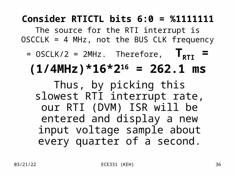
The source for the RTI interrupt is OSCCLK = 4 MHz, not the BUS CLK frequency = OSCLK/2 = 2MHz.
Therefore, TRTI = (1/4MHz)*16*216 = 262.1 ms
Thus, by picking this slowest RTI interrupt rate, our RTI (DVM) ISR will be entered and display a new input
voltage sample about every quarter of a second.
Consider RTICTL bits 6:0 = %1111111

04/18/23 ECE331 (KEH) 37
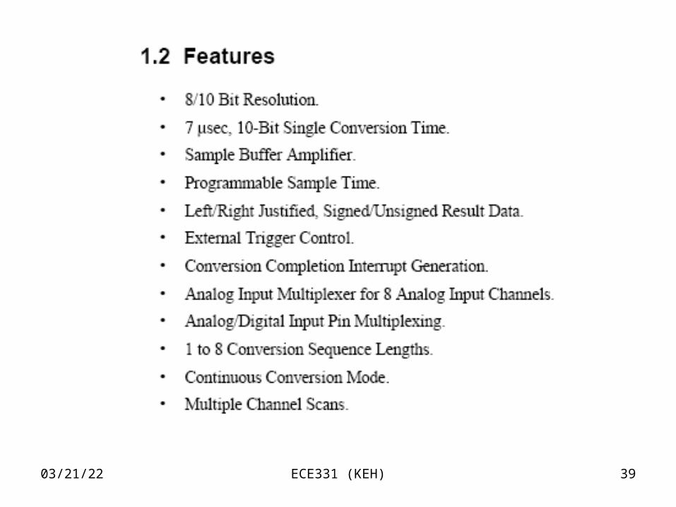
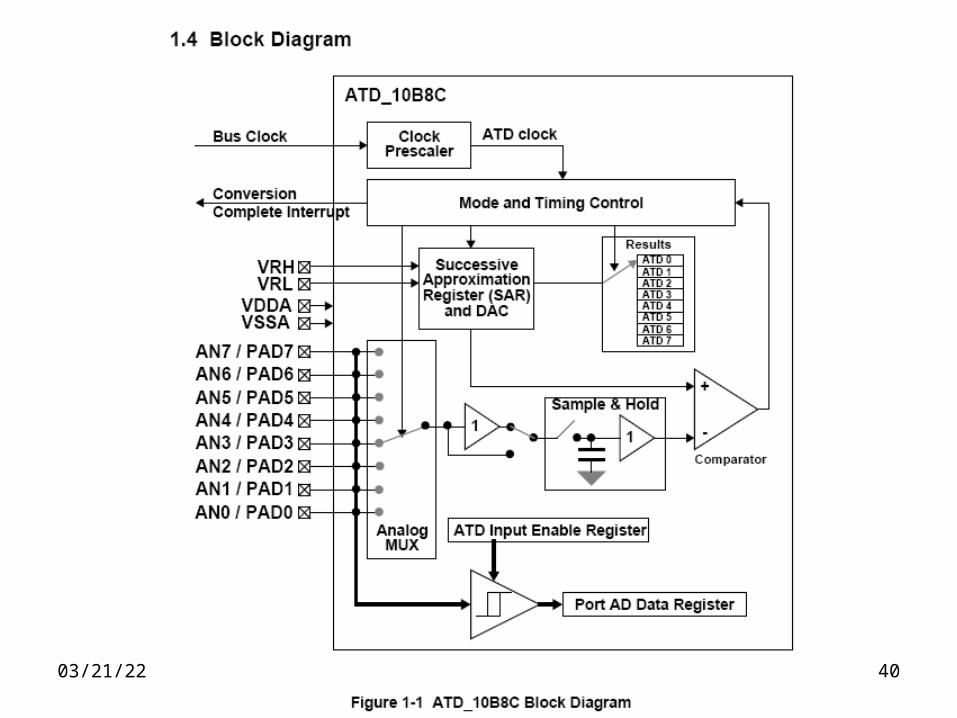
Analog-to-Digital (ATD) Converter

04/18/23 ECE331 (KEH) 38
Analog-to-Digital (ATD) Converter
• 9S12 microcontroller has one A/D converter with a 1 out of 8 analog input selection MUX (PORTAD Pins 7:0).
• When configured for single channel conversions, a conversion is started by writing a channel number to the ATDCTL5 control register.
• Then loop on the “sequence complete flag” (SCF), which is the MSB of the ATDSTAT0 register. Wait for SCF to go to 1, before reading the (10-bit) converted result from the result registers ATDDRxH and ATDDRxL.
04/18/23 ECE331 (KEH) 39
04/18/23 ECE331 (KEH) 40

04/18/23 ECE331 (KEH) 41
ATDDIEN – ATD Digital Input Enable Register
If DDRADx = 0, then ATDDIENx must be set in order to use pin PTADx (also called ANx) as a digital input pin, and cleared in order to use pin PTADx as an analog input pin.
If DDRADx = 1, then PTADx is a digital output, regardless of the setting of ATDDIENx.

04/18/23 ECE331 (KEH) 42
ATDCTL2 Control Register(ATDCTL0 and ADTCTL1 not used)
ADPU must be set to 1 to power up the ATD subsection. The other bits may remain 0. You must wait for at least 1 ms after powering up the ATD before it can be used, so be sure to set this bit to one at the very beginning of your program, well before the first RTI interrupt occurs.

04/18/23 ECE331 (KEH) 43
ATDCTL3 – Select single conversion per sequence

04/18/23 ECE331 (KEH) 44
ATDCTL4 – Select 10-bit conversion, 2-clock sample time, and 1/16 ATD Clock prescaling value
04/18/23 ECE331 (KEH) 45
04/18/23 ECE331 (KEH) 46
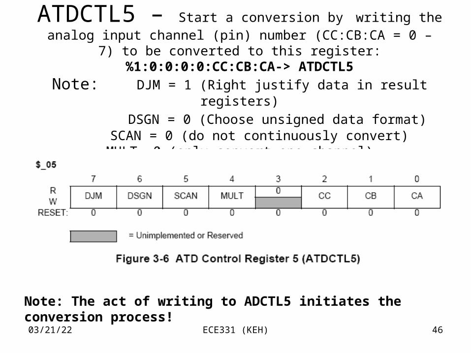
ATDCTL5 – Start a conversion by writing the analog input channel (pin) number (CC:CB:CA = 0 – 7) to be converted to this
register: %1:0:0:0:0:CC:CB:CA-> ATDCTL5
Note: DJM = 1 (Right justify data in result registers)
DSGN = 0 (Choose unsigned data format) SCAN = 0 (do not continuously convert)
MULT =0 (only convert one channel)
Note: The act of writing to ADCTL5 initiates the conversion process!

04/18/23 ECE331 (KEH) 47
ATDSTAT0 – ATD Status RegisterWait for SCF (sequence complete flag to be set before reading the converted result from
the result registers)
04/18/23 ECE331 (KEH) 48
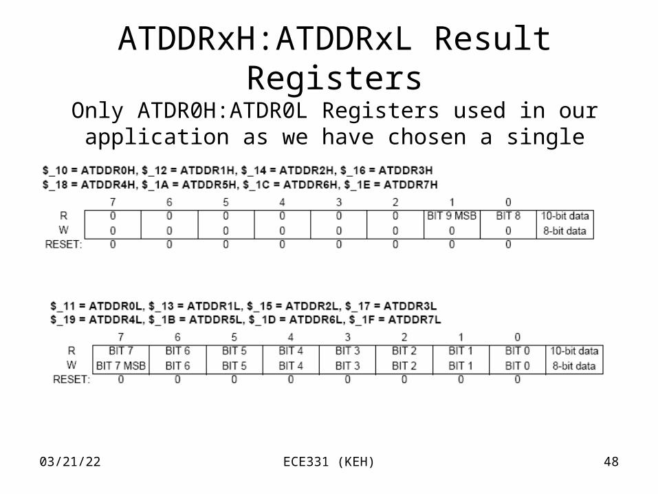
ATDDRxH:ATDDRxL Result RegistersOnly ATDR0H:ATDR0L Registers used in our application
as we have chosen a single conversion sequence.

04/18/23 ECE331 (KEH) 49
Serial Peripheral Interface
(SPI)

04/18/23 ECE331 (KEH) 50
SPI Port Overview• We shall write a data byte to the SPI Data
Register (SPIDR), to cause it to be serially shifted out of the serial output (MOSI) pin.
• The serial clock (SCK) pin is configured to generate a rising edge in the middle of each of the 8 data bit times, to permit the MOSI data to be shifted into an external “SLAVE” (74HC595) shift register.
• We shall loop on the SPI status register (SPISR) “SPTEF” (SPI Transmit Register Empty Flag) bit to know when the serial transmission is complete, and then a new byte may be written to the SPIDR.
04/18/23 ECE331 (KEH) 51
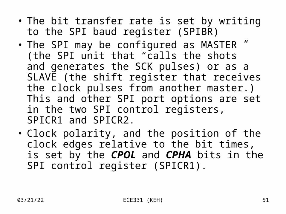
• The bit transfer rate is set by writing to the SPI baud register (SPIBR)
• The SPI may be configured as MASTER (the SPI unit that “calls the shots” and generates the SCK pulses) or as a SLAVE (the shift register that receives the clock pulses from another master.) This and other SPI port options are set in the two SPI control registers, SPICR1 and SPICR2.
• Clock polarity, and the position of the clock edges relative to the bit times, is set by the CPOL and CPHA bits in the SPI control register (SPICR1).

04/18/23 ECE331 (KEH) 52

04/18/23 ECE331 (KEH) 53
SPI Pins PM4=MOSI,PM2=MISO, PM3=SS\, PM5=SCK)

04/18/23 ECE331 (KEH) 54
Our DVM SPI Application
• Our application involves only serial output, so only MOSI (PM4) and SCK (PM5) pins will be used.
• The Slave Select (SS\) SPI pin function (PM3) will be disabled so this pin (PM3) can be used as a general-purpose I/O pin to present a rising edge on the RCLK pins of the 74HC595 shift registers.
• Recall that the RCLK pin is used to transfer the shift register into the holding register, and thus present the shifted data to the outside world.

04/18/23 ECE331 (KEH) 55
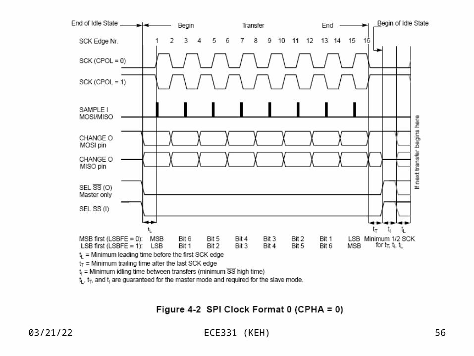
SPI Control Register 1
SPIE = 0, SPTIE = 0 (Disable SPI interrupts)
SPE = 1 (Enable SPI module)
MSTR = 1 (Make the 9S12C’s SPI port the MASTER SPI port. It would
be made a SLAVE if other 9S12C’s were to communicate.)
CPOL=1, CPHA=1 (Make clock RISE in middle of data bit times. See following timing diagrams.)
SSOE = 0 (Disconnect SS\ pin from SPI system, so it is freed up for use as a general-purpose I/O pin.)
LSBFE = 0 (Transfer data most-significant bit first.)
04/18/23 ECE331 (KEH) 56

04/18/23 ECE331 (KEH) 57

04/18/23 ECE331 (KEH) 58
SPI Baud Rate Register

04/18/23 ECE331 (KEH) 59
In order for the SPI to do its job as quickly as possible, thereby shortening the length of the DVM interrupt routine, I suggest using a reasonably fast baud rate that is still compatible with the 74HC595 maximum allowable clock rate (21 MHz).
From the design equations in Section 3.1.3 of S12SPIV3.pdf, setting SPPR2:0 = %010 and SPR2:0 =%011 should yield
BAUDRATE = bus clock / {(SPPR + 1)*(2SPR+1)} = 2 MHz/{3*(24)} = 41.667 kHz.
Recommended Baud Rate Setting
04/18/23 ECE331 (KEH) 60
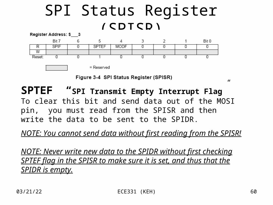
SPI Status Register (SPISR)
SPTEF “SPI Transmit Empty Interrupt Flag” To clear this bit and send data out of the MOSI pin, you must read from the SPISR and then write the data to be sent to the SPIDR.
NOTE: You cannot send data without first reading from the SPISR!
NOTE: Never write new data to the SPIDR without first checking SPTEF flag in the SPISR to make sure it is set, and thus that the SPIDR is empty.

04/18/23 ECE331 (KEH) 61
SPIF “SPI Transfer Finished” flag.
The difference between this flag and the SPTEF flag is that SPIF is set when the shift register is entirely empty and the serial transfer is complete. The SPTEF bit is set when the SPIDR is empty, and so another character to be sent can then be written to the SPIDR. However, keep in mind that when the SPTEF bit goes high, the SPIDR may be empty, but the SPI shift register may still be in the process of sending the previous character.
Like the SPTEF bit, to clear this bit, you must read from the SPISR and then either read the SPIDR or write the data to the SPIDR.
04/18/23 ECE331 (KEH) 62
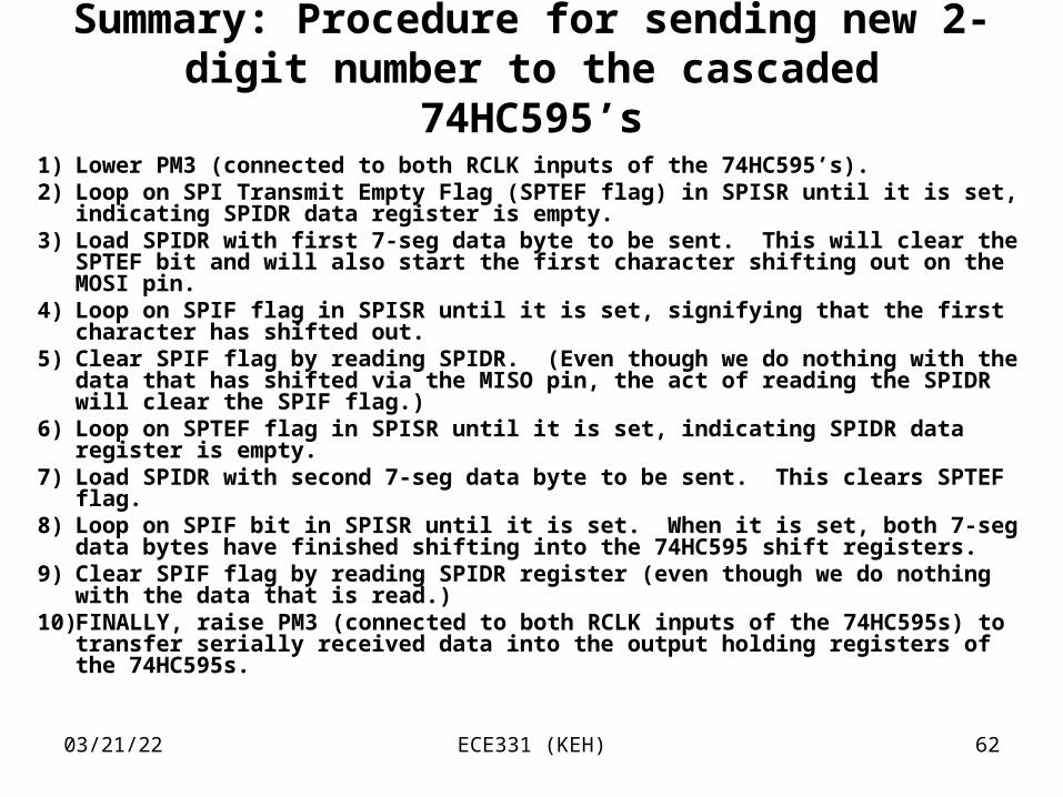
Summary: Procedure for sending new 2-digit number to the cascaded 74HC595’s
1) Lower PM3 (connected to both RCLK inputs of the 74HC595’s).2) Loop on SPI Transmit Empty Flag (SPTEF flag) in SPISR until it is set, indicating
SPIDR data register is empty.3) Load SPIDR with first 7-seg data byte to be sent. This will clear the SPTEF bit and
will also start the first character shifting out on the MOSI pin.4) Loop on SPIF flag in SPISR until it is set, signifying that the first character has
shifted out.5) Clear SPIF flag by reading SPIDR. (Even though we do nothing with the data that
has shifted via the MISO pin, the act of reading the SPIDR will clear the SPIF flag.)6) Loop on SPTEF flag in SPISR until it is set, indicating SPIDR data register is empty.7) Load SPIDR with second 7-seg data byte to be sent. This clears SPTEF flag.8) Loop on SPIF bit in SPISR until it is set. When it is set, both 7-seg data bytes have
finished shifting into the 74HC595 shift registers.9) Clear SPIF flag by reading SPIDR register (even though we do nothing with the data
that is read.)10) FINALLY, raise PM3 (connected to both RCLK inputs of the 74HC595s) to transfer
serially received data into the output holding registers of the 74HC595s.
04/18/23 ECE331 (KEH) 63
Initialization Steps to be added to Main Program
First set the Port M Data Direction Register (DDRM) to make pins PM5, PM4, and PM3 all outputs. (Unlike the input capture and output compare pins, the SPI pins do not automatically become outputs without the corresponding DDRM bits being set to 1.)
Then properly set the serial peripheral interface control register 1 (SPICR1) to enable the SPI, disable the SPI interrupt, set the SPI to “master mode”, and select the proper SPI clock phase and polarity (CPOL and CPHA) suitable for clocking 8-bits of data out of the Master Out Slave In, or “MOSI” pin (Pin PM4), using the SPI’s serial Clock “SCK” pin, assuming a rising-edge sensitive serial-in, parallel-out shift register (74HC595).
The proper choice of the CPOL and CPHA bits (see Fig. 4-2 and Fig. 4-3 of S12SPIV3.pdf ) is very important, because you want to allow adequate set-up and hold-time for the external shift registers, that is, the data must be held steady well before and also well after the rising of the clock, and thus you want to have the clock rise in the middle of the time that each of the 8 data bits is held valid.

04/18/23 ECE331 (KEH) 64
Tasks of the DVM (RTI) Interrupt Routine
– Clear the RTI interrupt flag. (Write a 1 to RTIF flag in the MSB of CRGFLG register.)
– Start an ATD conversion on channel 7 (by writing $87 to ATDCTL5), and wait until it is done by looping on the Sequence Complete Flag (SCF), which is the MSB of ATDSTAT0.
– Convert the result to a range of 0 - 50. Load “D” with the 10-bit converted result “R”, which is in the range of 0 ($0000) to 1023 ($03FF), from ATDDR0H:ATDDR0L (result must be right justified). Now multiply “D” by 50, then add 25 for rounding, and finally divide this result by 1024.
– Convert the result to BCD. Conversion to BCD can be done by a single division by 10. For example, the value $26 divided by 10 yields 3 with a remainder of 8, and the decimal value of $26 is 38.

04/18/23 ECE331 (KEH) 65
– Convert the two BCD digits into their corresponding 7-segment representation by indexing into a lookup table, which you have placed in flash program memory using the form constant byte (FCB) directive. The entries in this lookup table depend upon how you have your segments wired to your shift register.
– Send the 7-segment data for each display out of the SPI port. Do this by following these steps:
1. Lower PM3 (the 74HC595 RCLK inputs). 2. Loop until the SPI Transmit Empty flag (SPTEF), which is Bit #5 of the SPISR,
goes to 1, to indicate the SPIDR register is empty.3. Write the first byte of data into the SPI data register (SPIDR). This also clears
SPTEF flag.4. Loop on the SPI Finished (SPIF) flag, which is Bit #7 of the SPISR, goes to 1. 5. Clear SPIF flag by reading SPIDR (even though we do nothing with what is read).6. Loop until the SPI Transmit Empty flag (SPTEF), which is Bit #5 of the SPISR,
goes to 1, to indicate the SPIDR register is empty.7. Then write the second byte of data into the SPI data register (SPIDR). This also
clears SPTEF flag.8. Loop on the SPI Finished flag (SPIF), which is Bit #7 of the SPISR, goes to 1,
which indicates both data bytes have been completely shifted into the external 74HC595 shift registers.
9. Clear SPIF flag by reading SPIDR (even though we do nothing with what is read).10. Raise PM3 (the 74HC595’s RCLK inputs) in order to clock the newly shifted data
into the 74HC595’s output holding register.

04/18/23 ECE331 (KEH) 66
Remember that the length of this interrupt service routine must be kept as short of possible.
Hopefully, all of this can be done fast enough that it does not keep other time-critical interrupts that might occur at the time this one is being processed from waiting too long.
The good news is that this interrupt will occur relatively infrequently… only once every 262.2 ms.
Related Documents