Paul Scherrer Institut • 5232 Villigen PSI ESLS-RF - Oct, 2007 M. Gaspar 60KW 500 MHZ Solid State Amplifier Design Progress Report M. Gaspar, M. Pedrozzi

Welcome message from author
This document is posted to help you gain knowledge. Please leave a comment to let me know what you think about it! Share it to your friends and learn new things together.
Transcript

Paul Scherrer Institut • 5232 Villigen PSI ESLS-RF - Oct, 2007 M. Gaspar
60KW 500 MHZ Solid State Amplifier Design Progress Report
M. Gaspar, M. Pedrozzi
Paul Scherrer Institut • 5232 Villigen PSI ESLS-RF - Oct, 2007 M. Gaspar
Commissioning of 4KW Validation Prototype
PC Master Controller: Design Finished. 5 Pieces to be Ordered (Industry)
Power Supply Controller: Design Finished. 50 Pieces in Production (Industry)
Power Splitter: 2 8-Way Prototypes Working (PSI Design)
250W Amplifier Module: All Parts Available (Incl. Substrates). Assembly & Tests in House.
Cooling Bar: Use Soleil Design (Keep Compatibility) (Industry)
High Power Coupler: to be Purchased (Industry)
Output Power Combiner: 18-Way Combiner in Production (PSI Workshop)
Cables: to be Purchased (Industry)
Water Cooled Load: to be Purchased (Industry)
Paul Scherrer Institut • 5232 Villigen PSI ESLS-RF - Oct, 2007 M. Gaspar
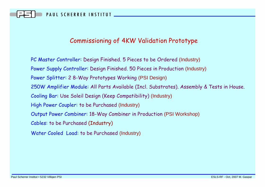
4KW Amplifier Configuration

Paul Scherrer Institut • 5232 Villigen PSI ESLS-RF - Oct, 2007 M. Gaspar
250W Amplifier Module
Key Performance Parameters
3D-View of 500MHz Amplifier Module
~ 50%~ 54%Efficiency
20dB22dBGain
280W250WOutput Power(with Circulator)
MaxOperation
Pout(W) vs Pin(W)
0
50
100
150
200
250
300
0 0.2 0.4 0.6 0.8 1 1.2 1.4 1.6 1.8 2
Pin(W)
Pou
t(W)
Pout (dBm)
Phase(S21) (°) vs Pout(W)
80.00
90.00
100.00
110.00
120.00
130.00
140.00
150.00
0 50 100 150 200 250 300
Pout(W)
Pha
se(S
21) (
°)
Phase (°)
New Design using LDMOS MRF6P3300

Paul Scherrer Institut • 5232 Villigen PSI ESLS-RF - Oct, 2007 M. Gaspar
9 Way Combiner – 500MHz
All Parts Available
Not Yet Assembled
Tests in Preparation
Status
Paul Scherrer Institut • 5232 Villigen PSI ESLS-RF - Oct, 2007 M. Gaspar
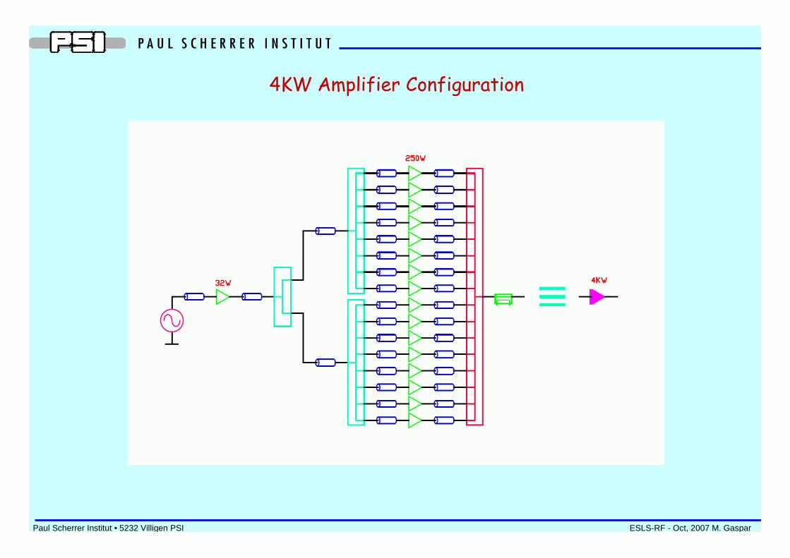
18/16 Way Combiner – 500MHz
Mechanical Parts in Production Now
Precision Required for 18 Ways will be Realized withno Extra Costs
Tests in Preparation
Status
Paul Scherrer Institut • 5232 Villigen PSI ESLS-RF - Oct, 2007 M. Gaspar
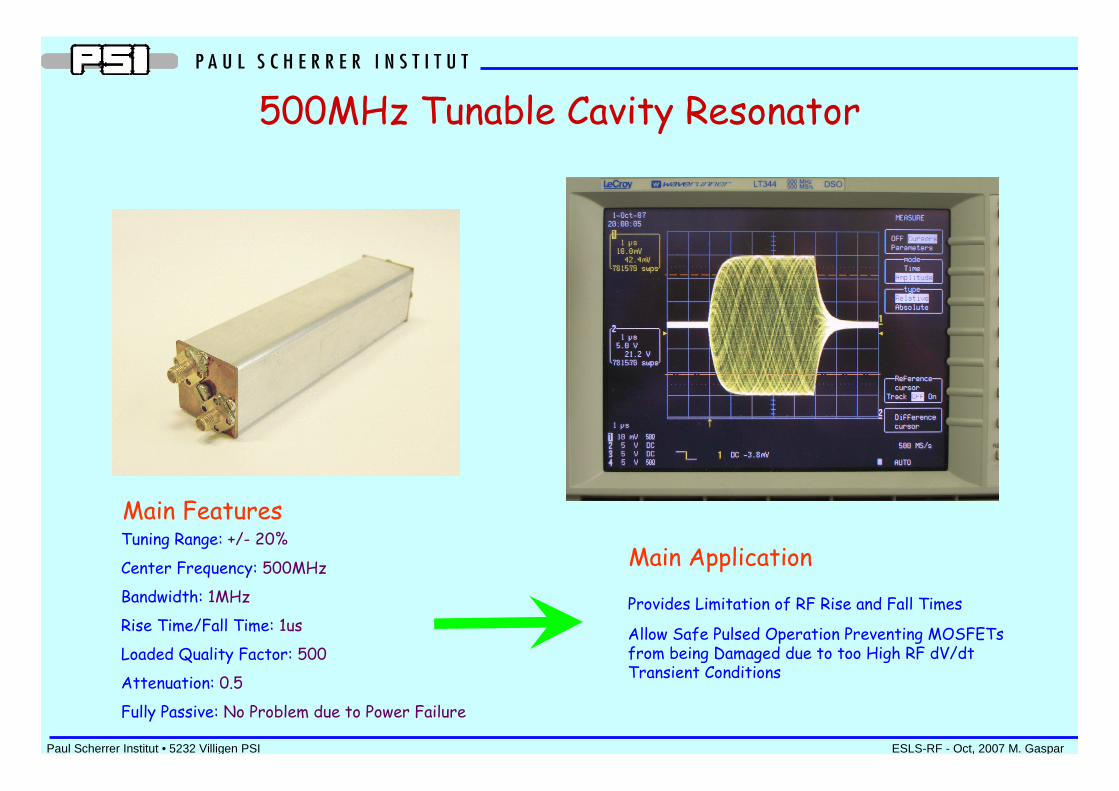
500MHz Tunable Cavity Resonator
Tuning Range: +/- 20%
Center Frequency: 500MHz
Bandwidth: 1MHz
Rise Time/Fall Time: 1us
Loaded Quality Factor: 500
Attenuation: 0.5
Fully Passive: No Problem due to Power Failure
Main Features
Provides Limitation of RF Rise and Fall Times
Allow Safe Pulsed Operation Preventing MOSFETsfrom being Damaged due to too High RF dV/dtTransient Conditions
Main Application
Paul Scherrer Institut • 5232 Villigen PSI ESLS-RF - Oct, 2007 M. Gaspar
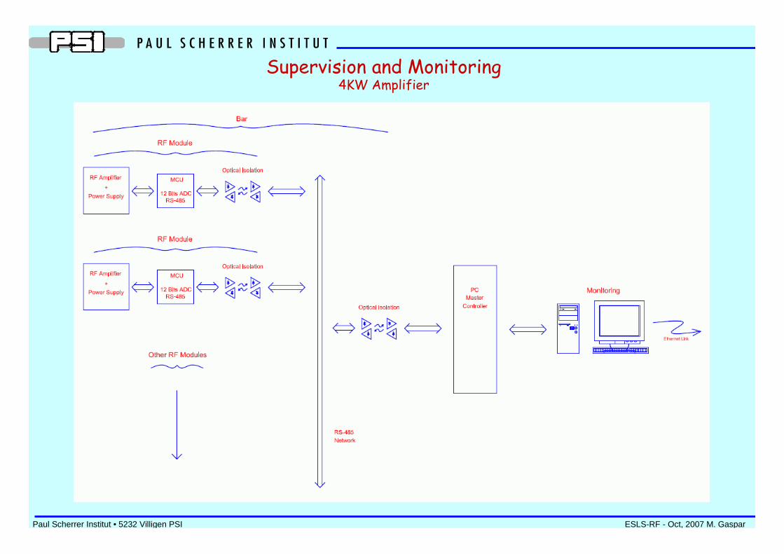
Supervision and Monitoring4KW Amplifier

Paul Scherrer Institut • 5232 Villigen PSI ESLS-RF - Oct, 2007 M. Gaspar
Power Supply Controller(and Complete Monitoring System)
RS485Network
Power SupplyOutput
AmplifierMonitoring
Extra DigitalI/Os
Extra AnalogI/Os
DC/DC Converter
High Voltage Input and Filtering
Output Power: 600W
Output Voltage Range: 16.7V to 33.5V
Input Voltage Range: 200V to 400V
Efficiency: ~ 90%
Can be Remotely Programmed and Monitored
Extra Analog and Digital I/Os
Multi-tasking Script Operating System (SOS)
Interlock Reaction Time: ~ 1uS
Full Monitoring Loop Time: ~ 150mS
Main Features
50 Pieces in Production Now
LEDs for Interlock and operation
Design Finished

Paul Scherrer Institut • 5232 Villigen PSI ESLS-RF - Oct, 2007 M. Gaspar
SOS (Save Our Souls)(Originally: Script Operating System*)
Runs ASCII Scripts: No Need for Previous Compilation
Available Commands for Analog and Digital I/O
Simplified IBM BSC Protocol implementation for Network Applications
Can also be used in Autonomous Applications (No Network)
Optimized for Data Acquisition
Multi-tasking Environment: Allows Monitoring and Data Taking Simultaneously
Precise Time-Base for Timing Applications: 1mS
Almost all Code Portable to other Microcontrollers
Designed in House: No Commercial Licen$e Needed
Main Features
Actual Version: SOS v2.96.26
* Original name was “Script Operating System”. New Name “Save Our Souls” was Kindly Proposed by our Colleague Pal Trivan
Will be Programmed in All New PowerSupply Controllers in Production Now

Paul Scherrer Institut • 5232 Villigen PSI ESLS-RF - Oct, 2007 M. Gaspar
PC Master Controller
RS485Network
USBConnection
Standard Europa Format
Isolated Power Supply
Output Isolated Power: 15V 1A
Maximum Data Rate: 200Kbps
External Connections: USB and RS232
Interlock Monitoring through Signaling Lines
Main Features
5 Pieces to be Ordered
LEDs for Interlock and Operation
Design Finished
RS232Connection
Paul Scherrer Institut • 5232 Villigen PSI ESLS-RF - Oct, 2007 M. Gaspar
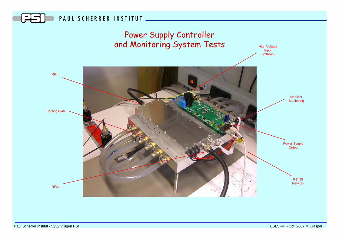
Power Supply Controllerand Monitoring System Tests
Power SupplyOutput
High VoltageInput
(220Vac)
RFin
AmplifierMonitoring
RS485Network
RFout
Cooling Plate

Paul Scherrer Institut • 5232 Villigen PSI ESLS-RF - Oct, 2007 M. Gaspar
RF Design Law
P = (W*t*N*M*p)* e + 2πS + H + L - G
Definitions:
P = Output Power
p = Input Power
W = A lot of Work
t = Lots of Extra Hours
T = Time
L = Passion for RF Design and Electronics
S = Personal Satisfaction
H = Proud of Making a High Quality and Interesting Work
M = Solid-State Device, Mosfet
N = Multiplication Number
G = Girlfriend‘s Unhappiness Correction Factor
K = Designer Dependent Constant
C = Designer‘s Competence and Knowledge
Conclusions
Physics Law
P = W / T
C-T/K
Related Documents