Rev 1.03 1 PA 5W HF PA kit assembly instructions 1. Introduction This is a Power Amplifier kit (PA) for CW or FSK modes, but with differences! The output power is approximately 5W in the middle of the HF frequency range, using a 13.8V supply. A single inexpensive IRF510 MOSFET is the amplification device. An unusual feature of this PA is the built- in facility for envelope shaping, which can create a precise raised-cosine keying envelope shape. This greatly reduces key-clicks when using on/off keyed modes such as CW or at the commencement/completion of an FSK mode transmission. The kit has a PCB of size 80 x 37mm, which is the same size as the other QRP Labs modules such as the Ultimate3S QRSS/WSPR transmitter kit, the VFO kit and the Relay-switched LPF kit. It is therefore physically (as well as electrically) compatible with the other QRP Labs kits and can be bolted behind them in the familiar PCB sandwich. Alternatively this PA can be used with your own homebrew projects. The PCB has space for SMA connectors (not supplied by default with the kit), if you wish to use SMA cables. A discrete component power modulator (voltage regulator) is controlled by an 8-bit R-2R Digital Analogue Converter, which allows an external microcontroller to control the amplitude of the output by loading the on-board 8-bit shift register using three I/O signals, and thereby create the raised cosine shape. The 8-bit shift register in the PA kit can optionally be replaced with an ATtiny84 microcontroller which will create the raised cosine profile without requiring an external microcontroller at all! This circuit contains many interesting, unusual and educational circuit blocks, and I would strongly encourage you to read the following theoretical explanation and understand everything before starting the assembly. The PA kit must always be followed by a low pass filter to attenuate unwanted transmitter harmonics, as usual for RF power amplifiers. There are many ways to build this PA kit. You do not have to use a microcontroller to generate a raised-cosine profile. You don’t have to build the power modulator either if you don’t want that facility. The complete design will be explained in this document, along with some description of how to omit various blocks if you wish. Carry out an inventory of the components according to the parts list to make sure all the components are present. Read the assembly instructions first before starting the assembly, understand everything, and then finally start the assembly, following all the steps carefully! I am deeply indebted to Alan G8LCO for his assistance in the design of many of the esoteric circuit blocks in the power modulator.

Welcome message from author
This document is posted to help you gain knowledge. Please leave a comment to let me know what you think about it! Share it to your friends and learn new things together.
Transcript

Rev 1.03 1
PA
5W HF PA kit assembly instructions
1. Introduction
This is a Power Amplifier kit (PA) for CW or FSK modes, but with differences! The output power is
approximately 5W in the middle of the HF frequency range, using a 13.8V supply. A single
inexpensive IRF510 MOSFET is the amplification device. An unusual feature of this PA is the built-
in facility for envelope shaping, which can create a precise raised-cosine keying envelope shape.
This greatly reduces key-clicks when using on/off keyed modes such as CW or at the
commencement/completion of an FSK mode transmission.
The kit has a PCB of size 80 x 37mm, which is the same size as the other QRP Labs modules
such as the Ultimate3S QRSS/WSPR transmitter kit, the VFO kit and the Relay-switched LPF kit.
It is therefore physically (as well as electrically) compatible with the other QRP Labs kits and can
be bolted behind them in the familiar PCB sandwich. Alternatively this PA can be used with your
own homebrew projects. The PCB has space for SMA connectors (not supplied by default with the
kit), if you wish to use SMA cables.
A discrete component power modulator (voltage regulator) is controlled by an 8-bit R-2R Digital
Analogue Converter, which allows an external microcontroller to control the amplitude of the
output by loading the on-board 8-bit shift register using three I/O signals, and thereby create the
raised cosine shape. The 8-bit shift register in the PA kit can optionally be replaced with an
ATtiny84 microcontroller which will create the raised cosine profile without requiring an external
microcontroller at all!
This circuit contains many interesting, unusual and educational circuit blocks, and I would strongly
encourage you to read the following theoretical explanation and understand everything before
starting the assembly.
The PA kit must always be followed by a low pass filter to attenuate unwanted transmitter
harmonics, as usual for RF power amplifiers.
There are many ways to build this PA kit. You do not have to use a microcontroller to generate a
raised-cosine profile. You don’t have to build the power modulator either if you don’t want that
facility. The complete design will be explained in this document, along with some description of
how to omit various blocks if you wish.
Carry out an inventory of the components according to the parts list to make sure all the
components are present. Read the assembly instructions first before starting the assembly,
understand everything, and then finally start the assembly, following all the steps carefully!
I am deeply indebted to Alan G8LCO for his assistance in the design of many of the esoteric circuit
blocks in the power modulator.

Rev 1.03 2

Rev 1.03 3
2. Parts list
Resistors
R27 0.33-ohm, 2 watt resistor
(none) 10-ohm resistor
R2, 19 15K resistor (2 pieces)
R4..10, 28 1.1K resistor (8 pieces)
R3, 11..18, 24 2.2K resistor (10 pieces)
R20, 22 3.3K resistor (2 pieces)
R21, 30 330-ohm resistor (2 pieces)
R23 8.2K resistor
R29 47K resistor
R1 4.7K trimmer potentiometer resistor
R26 3.3K resistor (not supplied)
R25 4.7K trimmer potentiometer resistor (not supplied)
Capacitors
C1..C3, C4..C8 1uF capacitor (7 pieces)
C4 1nF capacitor
Semiconductors
IC1 74HC595 8-bit shift register, 16-pin DIP package
IC2 7805L 5V regulator, TO92 package
Q3, 4 2N3904 NPN transistor, TO92 package
Q1, 2, 6, 8 2N3906 PNP transistor, TO92 package
Q5 2SC4242 NPN power transistor, TO220 package
Q7 IRF510 N-channel power MOSFET, TO220 package
Q9 BS170 N-channel MOSFET, TO92 package
Miscellaneous
16-pin socket 16-pin DIP socket for IC1
10-pin header 10-pin 0.1-inch header
Heatsink 65mm long PCB-mounting heatsink and pins
Insulation sets 2 pieces silicone rubber insulation pads + washers for the TO220 transistors
Nut and bolt 12mm long M3-size bolt and matching nut
FT50-43 FT50-43 toroid
Wire 100cm 0.33mm diameter wire
PCB 80 x 37mm Printed Circuit Board (PCB)

Rev 1.03 4
3. Theoretical circuit explanation
Here’s a block diagram of the PA circuit. Each of these circuit blocks will be described in turn.
3.1 Raised-cosine envelope shaping
Firstly it is important to understand what a raised cosine envelope is, and why we would want one
in a radio transmitter.
At the moment of switching on a radio transmission, the large instantaneous change in amplitude
caused by a sudden key-down causes a wide band spurious emission. The same thing happens
when the transmission is stopped (key-up). For a short time, the bandwidth is often many times
larger than the bandwidth of the modulated transmission which follows.
CW operators will be familiar with this phenomena which is often called “key clicks”. Some older
transmitters or simple homebrew transmitters suffer from this defect. Although your receiver (and
CW filter) may be tuned many hundreds of Hz away from the offending station such that you will
not hear his actual CW tone, you will be able to hear “clicks” every time he keys (starts or finishes
the envelope of a CW “dit” or “dah”). This creates annoying interference for other operators on
nearby frequencies.
Note that a transmission mode which uses Frequency Shift Keying (FSK) rather than On/Off
Keying (OOK), does not suffer from key clicks except at the start and the end of the message.
Envelope shaping is less important for FSK than for OOK modes such as CW.
A good conscientious operator will wish to minimise these “clicks”. This is accomplished by gently
switching on and off the RF power rather than hard-keying it on and off. If the key-down and key-
up follow a raised cosine shape then this is ideal.
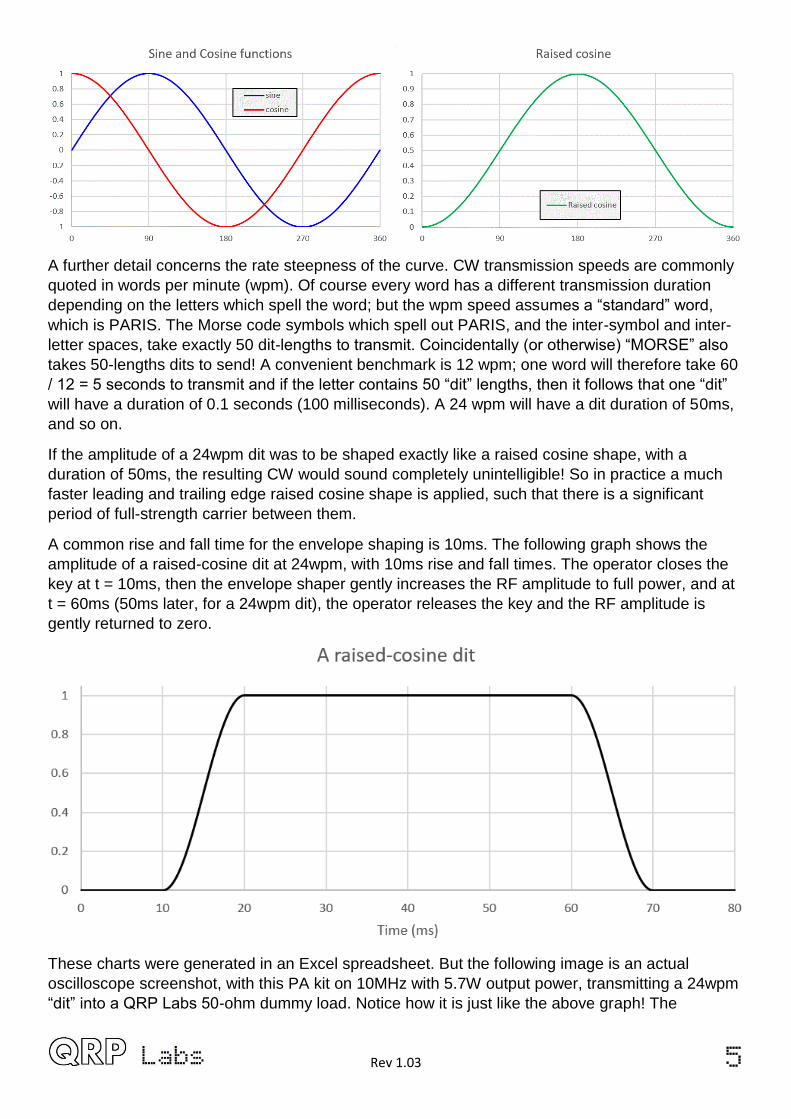
The following diagram illustrates sine and cosine functions (left). The cosine is the same shape as
the sine but has a 90-degree phase offset. It lags 90 degrees (a quarter of a cycle) behind the
sinewave. Now if the cosine function is shifted up, or “raised”, and normalised to the range 0..1
with the correct sign, then we have the shape shown (right). If this function is multiplied by the RF
envelope, amplitude-modulating the moment of key-down and key-up, then the hard “edges” are
eliminated and so are the “key clicks”!
Rev 1.03 5
A further detail concerns the rate steepness of the curve. CW transmission speeds are commonly
quoted in words per minute (wpm). Of course every word has a different transmission duration
depending on the letters which spell the word; but the wpm speed assumes a “standard” word,
which is PARIS. The Morse code symbols which spell out PARIS, and the inter-symbol and inter-
letter spaces, take exactly 50 dit-lengths to transmit. Coincidentally (or otherwise) “MORSE” also
takes 50-lengths dits to send! A convenient benchmark is 12 wpm; one word will therefore take 60
/ 12 = 5 seconds to transmit and if the letter contains 50 “dit” lengths, then it follows that one “dit”
will have a duration of 0.1 seconds (100 milliseconds). A 24 wpm will have a dit duration of 50ms,
and so on.
If the amplitude of a 24wpm dit was to be shaped exactly like a raised cosine shape, with a
duration of 50ms, the resulting CW would sound completely unintelligible! So in practice a much
faster leading and trailing edge raised cosine shape is applied, such that there is a significant
period of full-strength carrier between them.
A common rise and fall time for the envelope shaping is 10ms. The following graph shows the
amplitude of a raised-cosine dit at 24wpm, with 10ms rise and fall times. The operator closes the
key at t = 10ms, then the envelope shaper gently increases the RF amplitude to full power, and at
t = 60ms (50ms later, for a 24wpm dit), the operator releases the key and the RF amplitude is
gently returned to zero.
These charts were generated in an Excel spreadsheet. But the following image is an actual
oscilloscope screenshot, with this PA kit on 10MHz with 5.7W output power, transmitting a 24wpm
“dit” into a QRP Labs 50-ohm dummy load. Notice how it is just like the above graph! The

Rev 1.03 6
oscilloscope measures the peak-peak of the RF envelope, which is why there is a mirror-image in
the x-axis.
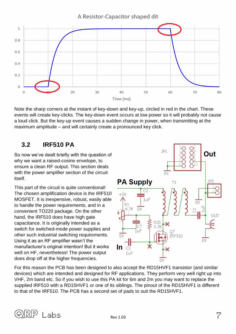
Resistor-Capacitor envelope shaping
It is also worth mentioning here a quite common misconception, which is that good key-shaping
can be achieved with a Resistor-Capacitor combination. It is often seen in simpler homebrew
transmitters and older equipment, and was even recommended in famous text books (which shall
remain nameless).
In fact, a Resistor-Capacitor has an exponential decay characteristic. It can help get reduce clicks
on key-down or key-up, but not both. It is better than nothing – but nowhere near as good as a
proper raised-cosine envelope shape.
The following graph is produced in an Excel spreadsheet numerically. It’s an RF envelope
amplitude shaped by a Resistor-Capacitor combination that produce an exponential shape to the
rising and falling edges.
Of course, in practice there will be non-linearities which may combine with the RC shape and
modify it, perhaps improving it – or maybe making it worse!
Rev 1.03 7
Note the sharp corners at the instant of key-down and key-up, circled in red in the chart. These
events will create key-clicks. The key-down event occurs at low power so it will probably not cause
a loud click. But the key-up event causes a sudden change in power, when transmitting at the
maximum amplitude – and will certainly create a pronounced key click.
3.2 IRF510 PA
So now we’ve dealt briefly with the question of
why we want a raised-cosine envelope, to
ensure a clean RF output. This section deals
with the power amplifier section of the circuit
itself.
This part of the circuit is quite conventional!
The chosen amplification device is the IRF510
MOSFET. It is inexpensive, robust, easily able
to handle the power requirements, and in a
convenient TO220 package. On the other
hand, the IRF510 does have high gate
capacitance. It is originally intended as a
switch for switched-mode power supplies and
other such industrial switching requirements.
Using it as an RF amplifier wasn’t the
manufacturer’s original intention! But it works
well on HF, nevertheless! The power output
does drop off at the higher frequencies.
For this reason the PCB has been designed to also accept the RD15HVF1 transistor (and similar
devices) which are intended and designed for RF applications. They perform very well right up into
VHF, 2m band etc. So if you wish to use this PA kit for 6m and 2m you may want to replace the
supplied IRF510 with a RD15HVF1 or one of its siblings. The pinout of the RD15HVF1 is different
to that of the IRF510. The PCB has a second set of pads to suit the RD15HVF1.
Rev 1.03 8
The incoming RF is coupled to the IRF510 gate via a 1uF capacitor. The largish 1uF value is
intended to help the PA work well on LF and MF. A DC bias voltage must be applied to the IRF510
gate, this is supplied by 4.7K preset potentiometer R1 via the 3.3K resistor R20.
A trifilar output transformer wound on an FT50-43 toroid provides matching to the 50-ohm output.
There are pads/holes on the PCB for an optional SMA connector. This is not supplied in the kit but
is available in the QRP Labs shop. You can also fit an SMA connector at the PA kit’s RF input
instead of the 2-pin header. The RF output is also available at the 2-pin header JP5, and at a 2 x
5-pin header JP1 (not supplied). The 2 x 5-pin header matches the headers on the Ultimate3S
QRSS/WSPR Transmitter PCB and the 6-band relay-switched filter kit PCB. This option may be
used when using this PA kit with Ultimate3S, and is described in an application note.
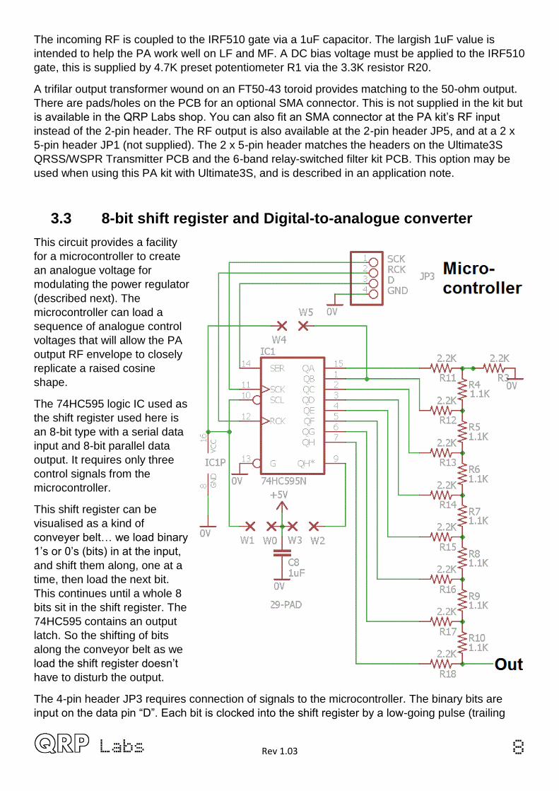
3.3 8-bit shift register and Digital-to-analogue converter
This circuit provides a facility
for a microcontroller to create
an analogue voltage for
modulating the power regulator
(described next). The
microcontroller can load a
sequence of analogue control
voltages that will allow the PA
output RF envelope to closely
replicate a raised cosine
shape.
The 74HC595 logic IC used as
the shift register used here is
an 8-bit type with a serial data
input and 8-bit parallel data
output. It requires only three
control signals from the
microcontroller.
This shift register can be
visualised as a kind of
conveyer belt… we load binary
1’s or 0’s (bits) in at the input,
and shift them along, one at a
time, then load the next bit.
This continues until a whole 8
bits sit in the shift register. The
74HC595 contains an output
latch. So the shifting of bits
along the conveyor belt as we
load the shift register doesn’t
have to disturb the output.
The 4-pin header JP3 requires connection of signals to the microcontroller. The binary bits are
input on the data pin “D”. Each bit is clocked into the shift register by a low-going pulse (trailing

Rev 1.03 9
edge) on the SCK pin. Finally when all 8 bits have been loaded into the shift register, a low-going
pulse (trailing edge) on the RCK pin latches the 8 loaded bits, and they then appear at the 8 output
pins of the 74HC595.
The next part of the circuit is the 8-bit Digital to Analogue Converter (DAC). The DAC employed
here is a simple resistor network known as an R-2R resistor ladder network. It is simple and
inexpensive, consisting of just 16 resistors. A “proper” DAC IC would be overkill in this application!
The resistor network is arranged such each bit makes a weighted contribution to the output
voltage. There are only two different resistor values in the network, whose values have a ratio of 2.
In this kit the resistor values are 1.1K and 2.2K. The result of the network is that the output voltage
is proportional to the value loaded in the 8-bit register IC1. An 8-bit binary number corresponds to
the decimal range 0..255. A value of 0 corresponds to an output voltage of 0V; a value of 255 will
generate an output voltage 1/256’th below the supply voltage of 5V, i.e. 4.98V.
It’s worth mentioning that 8 bits of accuracy are not really obtained in practice. The resistors in this
kit are 1% tolerance resistors. To really obtain an accurate resolution of 1/256 (8-bits) would
require finer tolerance resistors – but this would also increase the cost considerably! And again is
overkill for this application. If you really want to finesse the construction of this circuit, and you
have a means to accurately measure resistors, then measure all the resistors, and use the most
accurate ones (closest to 1.1K and 2.2K) at the most significant bits of the network, i.e. R18 and
R10. Work up the ladder as the values get less accurate. If you do this, you can probably achieve
the real 1/256’th resolution accurately!
5V voltage regulator
The PA kit contains a TO92-package 5V regulator IC type 78L05, IC2 (also equivalently called
7805L by some manufacturers). Note that this is shown on the main circuit diagram but in not the
sub-block above. This 5V is used by the shift register and DAC, the power modulator, and PA
bias. Providing the regulator on board simplifies the use of this PA kit module because you only
need to provide a single PA supply e.g. 13.8V. However do not be tempted to power other circuits
from this 5V regulator output, such as the Ultimate3S kit or other. The 78L05 is only a low power
voltage regulator and has no heatsink. The 78L05 is rated for 100mA maximum supply current.
On-board ATtiny84 option to generate the raised cosine
You will also note on the circuit diagram of the shift register and DAC, several jumper wire points
W0-W1, W2-W3, W4-W5. These are intended to provide yet another feature to this PA kit! This
document will describe the jumper connections for the 74HC595 shift register, to use an external
microcontroller to generate the raised cosine profile steps and load them into the shift register.
However, another use of the kit allows an ATtiny84 microcontroller to be plugged into the socket
instead of the 74HC595 IC. The ATtiny84 drives the 8-bit DAC directly, and generates the raised
cosine profile itself. This option is suitable for using the PA kit standalone as an amplifier for a
homebrew CW transmitter for example. A keying input is supplied, and the microcontroller
generates the raised cosine shape itself, with no external effort required.
This application of the PA kit is described in a separate application note, AN005.

Rev 1.03 10
3.4 Power modulator
Now we come to the most complex and interesting part of the PA kit circuit (the inspiration of Alan
G8LCO)! This power modulator could also be called a voltage regulator, controlled by the Digital to
Analogue Converter (DAC). It allows the microcontroller to vary the supply voltage to the IRF510
PA stage, and therefore to control the RF envelope, and create the desired raised-cosine shape.
It would have been possible, perhaps, to use something like a power operational amplifier for this
function. But this discrete component regulator is so much more fun and educational!
I’ll start by mentioning that the R25 preset potentiometer and R26 are NOT supplied in this kit.
They exist in the circuit diagram (and PCB) for people who do not wish to use the DAC under
micro-controller control to create a raised-cosine envelope, but who do wish to use the power
modulator just as a basic voltage regulator.
Probably the easiest way to
understand what this circuit is trying to
achieve, is to consider it as a power
operational amplifier.
The conventional way to consider an
operational amplifier with feedback is
that the op-amp is a black box which
tries to control its output voltage in
such a way that its two input voltages
are equal.
In the case of this circuit, the two
“inputs” are the bases of transistors Q1
and Q2; the “output” is the regulated
output voltage which powers the
IRF510 amplifier section. R23 and R24
form a potential divider in the feedback
network, which effectively sets the
output voltage at a multiple of the input
from the DAC.
Consider as an example what happens
when the DAC value is 100. The DAC
voltage will then be 5.0 x 100/256
which is 1.95V. This circuit wants to
keep the other input (the base of Q2)
also at a matching 1.95V. In order to
get 1.95V at Q2, the circuit output voltage must be 9.22V. This is because the voltage at Q2’s
base is 0.21 of the total output voltage – due to the R23-R24 potential divider. 2.2 / (2.2 + 8.2) =
0.21.
So, the circuit does what is necessary (imagine the black box op-amp case) to keep the output
voltage at 9.22V, regardless of the load and regardless of the supply voltage.

Rev 1.03 11
Differential amplifier
Transistors Q1, Q2, Q3 and Q4 are the differential amplifier. In the words of Alan G8LCO:
“So I designed something new, it’s a pair of complementary long tailed pairs interconnected as a
constant current side Q1,Q3 linked to a differential amplifier Q2,Q4. So you get a diff amp with 0V
inputs and very low offset voltage. I have not seen this before! So we should get effectively a DAC
controlled power supply. The four transistor arrangement can easily handle more than 36V which
is the tops for most Op amps and costs pennies. The four transistors have a pleasing layout too.”
Sziklai Pair
Now let’s consider the power output stage of this differential amplifier circuit. Ignore for the
moment R27, R28, R29 and Q8. Just consider the PNP Darlington pair Q5 and Q6. But wait!
That’s not a Darlington! A PNP Darlington pair would consist of two PNP transistors, but here we
see one PNP (Q6) and one NPN (Q5)!
This arrangement is called a “Sziklai pair” after George C Sziklai who popularised it. The
arrangement is also known variously as “Complementary Feedback Pair”, “compound transistor”
or “pseudo-Darlington”. It dates from the days when silicon power NPN transistors were not yet
available, but power PNP germanium transistors were. It was desirable to create a NPN power
transistor. This 2-transistor NPN-PNP pair made a power PNP transistor behave like a power NPN
transistor. The NPN device can be a small signal low power device, and the PNP device handles
all the power. The gain of the resulting “transistor” is the product of the two transistor gains, just
like in a real Darlington pair. The Sziklai pair has the advantage of a 0.6V base turn-on voltage
compared to 1.2V in a Darlington.
In our case here, necessity also motivated this choice of circuit! During development of this PA kit
the extensive facilities of the QRP Labs junk box was unavailable for some time, due to a QTH
move. Nowadays NPN transistors are much
more common than PNP. At least, in junk
boxes. The desired PNP Darlington power
transistor was therefore nowhere to be found,
not for love nor money. But NPN power
transistors, and small signal PNP transistors,
were available! So Sziklai rescued the situation
without needing to wait for shipment delays
when ordering real PNP Darlingtons from a
component distributor! Effectively the
combination of the PNP transistor Q6 and the
NPN power transistor Q5 in this PA circuit, acts
as a single PNP power transistor.
Technically a Sziklai pair was used historically
to create an NPN power transistor from PNP,
because NPN power transistors weren’t
available. But here I did the opposite… I created
a PNP transistor from NPN because PNP power transistors weren’t available! So it’s kind of
complementary-Sziklai (see right).
In any event – this little diversion was such a fascinating education for me that when it came to the
final PA kit production I did not use a power Darlington. Instead I have left this Sziklai pair in the
circuit, to be able to share this fascination with you!
Rev 1.03 12
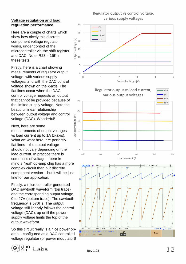
Voltage regulation and load
regulation performance
Here are a couple of charts which
show how nicely this discrete
component voltage regulator
works, under control of the
microcontroller via the shift register
and DAC. Note: R23 = 15K in
these tests.
Firstly, here is a chart showing
measurements of regulator output
voltage, with various supply
voltages, and with the DAC control
voltage shown on the x-axis. The
flat lines occur when the DAC
control voltage requests an output
that cannot be provided because of
the limited supply voltage. Note the
beautiful linear relationship
between output voltage and control
voltage (DAC). Wonderful!
Next, here are some
measurements of output voltages
vs load current up to 1A (x-axis).
What we want here, are perfectly
flat lines – the output voltage
should not vary depending on the
load current. In practice there is
some loss of voltage – bear in
mind a “real” op-amp chip has a more
complex circuit than our discrete
component version – but it will be just
fine for our application.
Finally, a microcontroller generated
DAC sawtooth waveform (top trace)
and the corresponding output voltage,
0 to 27V (bottom trace). The sawtooth
frequency is 570Hz. The output
voltage still linearly follows the control
voltage (DAC), up until the power
supply voltage limits the top of the
output waveform.
So this circuit really is a nice power op-
amp – configured as a DAC controlled
voltage regulator (or power modulator)!
Rev 1.03 13
Current limiting
Now let’s add current limiting to this voltage regulator! Of course this is fun and educational. But it
also serves a practical purpose, it will help to protect our components from destruction in the event
of short circuit. If you don’t know already from experience, you will be surprised by how many
power transistors you can fry in the course of experimenting with power amplifiers and voltage
regulators – and anything that can be done to help reduce this carnage must be beneficial!
Simple current limiting can be implemented just by adding R27, R28 and Q8. Please ignore R29
for now!
R27 is 0.33 ohms, a low enough value that not too much power is wasted in this component.
Remember Ohm’s law: V = I R. The voltage across this resistor R27 is the product of its resistance
and the current through it. At 1A current, the voltage will be 0.33V and at 2A current, the voltage is
0.66V. So you can see that at some point, as the voltage across R27 increases, eventually it
reaches a value that exceeds the 0.6V silicon junction base-emitter threshold of the transistor, and
it can switch on the PNP transistor Q8. “Switch” is not really the right word because in reality
there’s a curve, not a switching action. But it will suffice for the understanding of the circuit. When
Q8 switches on it will forcibly limit the current through the Q5/Q6 Sziklai PNP power transistor – by
dragging its base high (thereby reducing its
base-emitter voltage and turning it OFF).
This is simple current limiting.
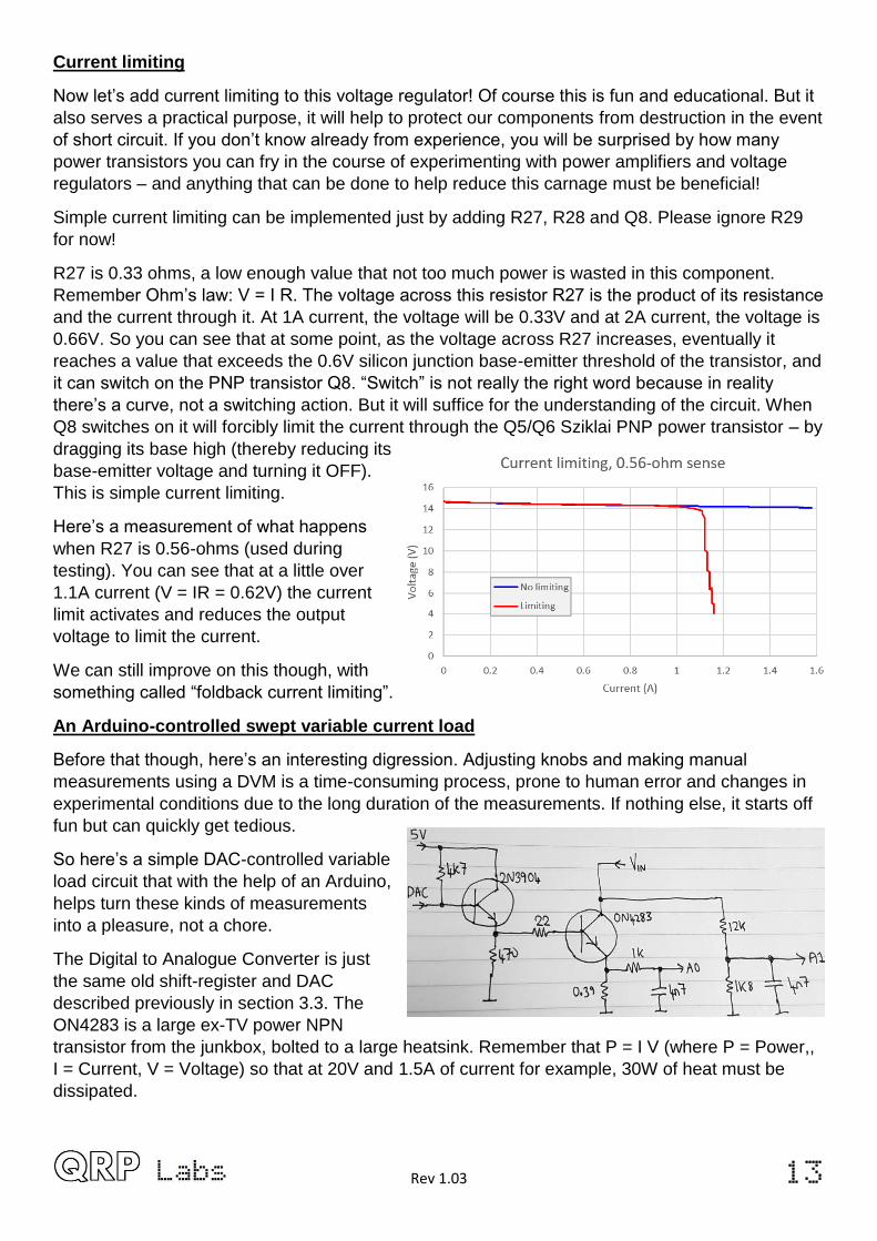
Here’s a measurement of what happens
when R27 is 0.56-ohms (used during
testing). You can see that at a little over
1.1A current (V = IR = 0.62V) the current
limit activates and reduces the output
voltage to limit the current.
We can still improve on this though, with
something called “foldback current limiting”.
An Arduino-controlled swept variable current load
Before that though, here’s an interesting digression. Adjusting knobs and making manual
measurements using a DVM is a time-consuming process, prone to human error and changes in
experimental conditions due to the long duration of the measurements. If nothing else, it starts off
fun but can quickly get tedious.
So here’s a simple DAC-controlled variable
load circuit that with the help of an Arduino,
helps turn these kinds of measurements
into a pleasure, not a chore.
The Digital to Analogue Converter is just
the same old shift-register and DAC
described previously in section 3.3. The
ON4283 is a large ex-TV power NPN
transistor from the junkbox, bolted to a large heatsink. Remember that P = I V (where P = Power,,
I = Current, V = Voltage) so that at 20V and 1.5A of current for example, 30W of heat must be
dissipated.

Rev 1.03 14
The 0.39-ohm resistor in the power transistor emitter circuit has a voltage across it proportional to
the load current, which is measured by the Arduino’s A0 Analogue to Digital Converter (ADC)
input. The A1 ADC input measures the applied voltage via a potential divider (1K8 and 12K
resistors).
Now it is a fairly simple Arduino sketch to load the shift register with a value, stepping from 0 to
255, and on each step pause, measure the ADC values A0 and A1, and repeat on the next step.
The measured A0 and A1 values can be sent to the Arduino serial monitor on the PC, so that the
set of 256 measured points can be copy-and-pasted into an Excel spreadsheet to generate nice
charts!
Foldback current limiting
Now back to the discussion on current limiting. The previous simple current limiting acted upon the
regulator output voltage, reducing it to limit the current. But this is not what we really want. What
we really want to do is limit the POWER dissipated in the Q5 power transistor, since it is heat that
fries components to destruction, not current.
As an example, consider again P = I V. So in the previous example, suppose the supply voltage to
the kit was 20V, and the current limit set to 1.1A. If the output voltage dropped to 4V to limit the
load current, then the transistor has 16V across it; and 16 x 1.1 means the transistor must now
dissipate 17.6W of power, a considerable amount that will quickly raise the temperature. So if we
want to protect our Q5 transistor, we need to limit power dissipation, not just current.
Fortunately, this is very easy to do, by the addition of a single extra resistor, R29 (47K). This
applies some current to the base of Q8 from the regulator output voltage. It is a form of positive
feedback that adds to the current measured across the 0.33-ohm resistor R27. The effect is that
once the current limit kicks in, both the voltage AND the current are reduced, which cuts the power
dissipation, saving our precious Q5 power transistor.
The values of the components now require some experiment to determine. The positive feedback
alters the required value of R27. The following graph shows a set of swept measurements with
R27 = 0.56-ohms and varying the value of the R29 foldback feedback resistor. The shape of these
V-I curves also explain why the technique is called “foldback” current limiting – because the
current folds back under the curve!

Rev 1.03 15
The final values chosen for R27 and R29
are 0.33-ohms and 47K respectively,
with R28 as 1.1K. This is quite close to
the measurement shown here (right) with
R29 = 50K and R28 = 1K. The final
component values in the kit were
changed to 1.1K instead of 1K, because
the kit already contains a pile of 1.1K
resistors in the DAC. It simplifies and
lowers the cost of the kitting process to
reduce the number of different
component values used. R29 was
changed from 50K to 47K to suit readily
available resistor values.
The current limit occurs at 1.6A. This is somewhat higher than we are likely to encounter in the
normal operating conditions of the PA, so the current limit will not be incorrectly initiated in normal
operation. On the other hand 1.6A is still low enough that it will provide protection against short
circuit conditions or other accidental abuse.
In order to reset the current limit, the power to the whole PA may need to be switched off and on
again.
This completes the description of the discrete component voltage regulator circuit (or “power
modulator”), with microcontroller control via an 8-bit shift register and DAC circuit. The
microcontroller can program a series of power modulator output voltages in quick succession, to
create a raised cosine profile of the RF envelope: the desired click-free outcome!
3.5 Leakage gate
The final circuit block to consider is the leakage gate, at the input
to the IRF510.
In practice it is found that even when the power modulator
voltage is at 0V (or I should say 0.15V, which is as close to zero
as it gets) and so the IRF510 is doing nothing at all, RF can still
leak through to the output. I measured 3.5V peak-peak at 10MHz
using an Ultimate3S as the driver to provide RF input. It is
desirable to attenuate the input signal, hence my name for it:
“leakage gate”.
The requirements on this “gate” are quite strenuous and
therefore difficult to achieve. It should:
• Eliminate leakage when the gate is “closed” (off), i.e. power modulator is at 0V output
• Not distort the linearity of the ratio of RF output envelope to DAC control voltage across the
entire DAC control voltage range 0..5V
• Not attenuate the drive signal significantly when the gate is open (on); since the gate
capacitance of the IRF510 is high, we cannot afford to attenuate the signal which would
decrease the final maximum output power.
Rev 1.03 16
The gate circuit using a BS170 MOSFET switch is shown (right) and was determined by a great
deal of experiment.
The initial idea may be understood by pretending that R21 is not in the circuit. In this case C6 and
C3 block DC, so that only AC signal flows through this gate circuit. That means that we are free to
add some bias to the BS170 MOSFET at the source pin, here this is R30 (330-ohms). The power
modulator voltage is connected directly to the gate of the BS170 transistor Q9. When the power
modulator is zero, the BS170 is off (high impedance) blocking the RF flow through from the RF
input connector to the IRF510. When the power modulator rises above the BS170 gate threshold
voltage, it will switch on the BS170, allowing the RF to flow through to the IRF510.
The BS170 has a static ON resistance of typically only 2 ohms. The typical gate threshold voltage
is 2V. Putting 2 ohms into the signal path does not damage the maximum output power
significantly.
The real behaviour differs from the simple explanation above. In practice the BS170 is of course
not a simple on/off switch. The incoming RF is also rectified by the BS170 and contributes to the
gate voltage, altering the gate-source resistance, which in turn again affects the rectification and
contribution to the gate voltage. So it’s a rather complex dynamic situation.
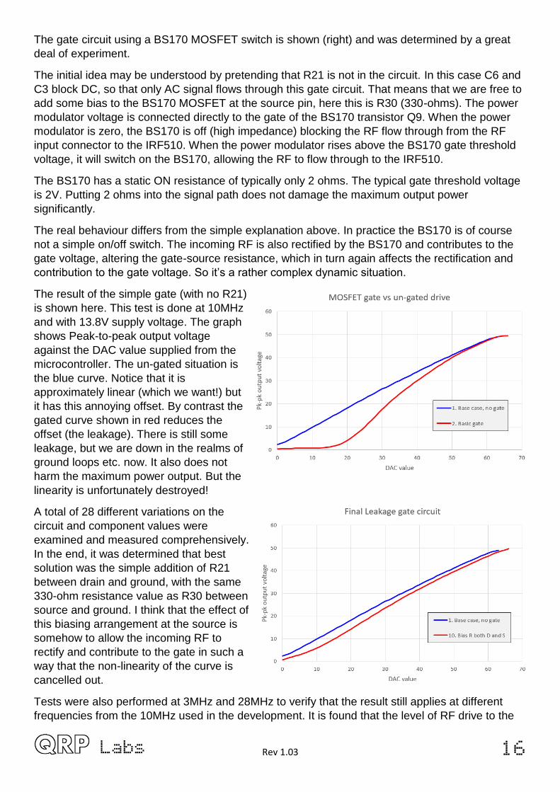
The result of the simple gate (with no R21)
is shown here. This test is done at 10MHz
and with 13.8V supply voltage. The graph
shows Peak-to-peak output voltage
against the DAC value supplied from the
microcontroller. The un-gated situation is
the blue curve. Notice that it is
approximately linear (which we want!) but
it has this annoying offset. By contrast the
gated curve shown in red reduces the
offset (the leakage). There is still some
leakage, but we are down in the realms of
ground loops etc. now. It also does not
harm the maximum power output. But the
linearity is unfortunately destroyed!
A total of 28 different variations on the
circuit and component values were
examined and measured comprehensively.
In the end, it was determined that best
solution was the simple addition of R21
between drain and ground, with the same
330-ohm resistance value as R30 between
source and ground. I think that the effect of
this biasing arrangement at the source is
somehow to allow the incoming RF to
rectify and contribute to the gate in such a
way that the non-linearity of the curve is
cancelled out.
Tests were also performed at 3MHz and 28MHz to verify that the result still applies at different
frequencies from the 10MHz used in the development. It is found that the level of RF drive to the

Rev 1.03 17
PA kit influences the linearity of the Peak-to-peak output vs DAC control value. At very low levels
of drive the curve tends to return to the non-linear Red line in the previous paragraph. At 28MHz
the available drive is lower and this is also the case. However at all reasonable levels of drive
likely to be encountered in practical use, the linearity is good.
This “leakage gate” circuit therefore achieves a worthwhile 6-10dB reduction of the leakage
without impacting the final maximum power of the amplifier, and without significant distortion of the
linearity of the peak-to-peak output voltage to DAC ratio.
4. Assembly
This assembly section will assume that you are constructing the whole PA kit circuit as described
in the previous sections. However you may choose to omit the power regulator, or omit the
microcontroller controlled DAC circuit, or other blocks of the circuit. This may apply if you simply
want a basic power amplifier without waveform shaping or any other of these features included
here. These options are covered in a subsequent section. Therefore please read the whole thing
before starting assembly, and consider carefully what you are aiming to achieve.
Assembly of this kit is quite straightforward. The usual kit-building recommendations apply: work in
a well-lit area, with peace and quiet to concentrate. The IC (chips) and some of the other
semiconductors in the kit are sensitive to static discharge. Therefore observe Electrostatic
discharge (ESD) precautions. And FOLLOW THE INSTRUCTIONS!!
A jeweller’s loupe is really useful for inspecting small components and soldered joints. You’ll need
a fine-tipped soldering iron too. It is good to get into the habit of inspecting every joint with the
magnifying glass or jeweller’s loupe (like this one I use),
right after soldering. This way you can easily identify any
dry joints or solder bridges, before they become a
problem later on when you are trying to test the project.
It is always best to detect and correct any mistakes as
early as possible (immediately after soldering the
incorrect component). The board is quite compact, to fit
the required 80 x 37mm PCB dimensions. Removing a
component and re-installing it later is often very difficult!
All of the resistors in the kit are installed vertically,
because PCB space is limited. It was important to design
it to fit on an 80 x 37mm PCB for potential use with other QRP Labs kits such as the Ultimate3S
QRSS/WSPR transmitter. You will need to bend the resistor wires as shown in the picture below.
On the parts layout diagram there is a small circle around the hole where the body end of the
resistor should be installed. This is
not critical (resistors don’t care
which way around they are) but it is
recommended, just to try to ensure
that the folded over wire-end of the
resistor doesn’t touch any other
wire or metal part.
Rev 1.03 18
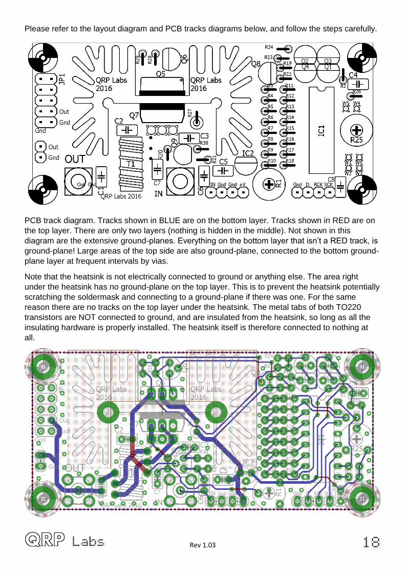
Please refer to the layout diagram and PCB tracks diagrams below, and follow the steps carefully.
PCB track diagram. Tracks shown in BLUE are on the bottom layer. Tracks shown in RED are on
the top layer. There are only two layers (nothing is hidden in the middle). Not shown in this
diagram are the extensive ground-planes. Everything on the bottom layer that isn’t a RED track, is
ground-plane! Large areas of the top side are also ground-plane, connected to the bottom ground-
plane layer at frequent intervals by vias.
Note that the heatsink is not electrically connected to ground or anything else. The area right
under the heatsink has no ground-plane on the top layer. This is to prevent the heatsink potentially
scratching the soldermask and connecting to a ground-plane if there was one. For the same
reason there are no tracks on the top layer under the heatsink. The metal tabs of both TO220
transistors are NOT connected to ground, and are insulated from the heatsink, so long as all the
insulating hardware is properly installed. The heatsink itself is therefore connected to nothing at
all.

Rev 1.03 19
4.1 Inventory parts
Rev 1.03 20
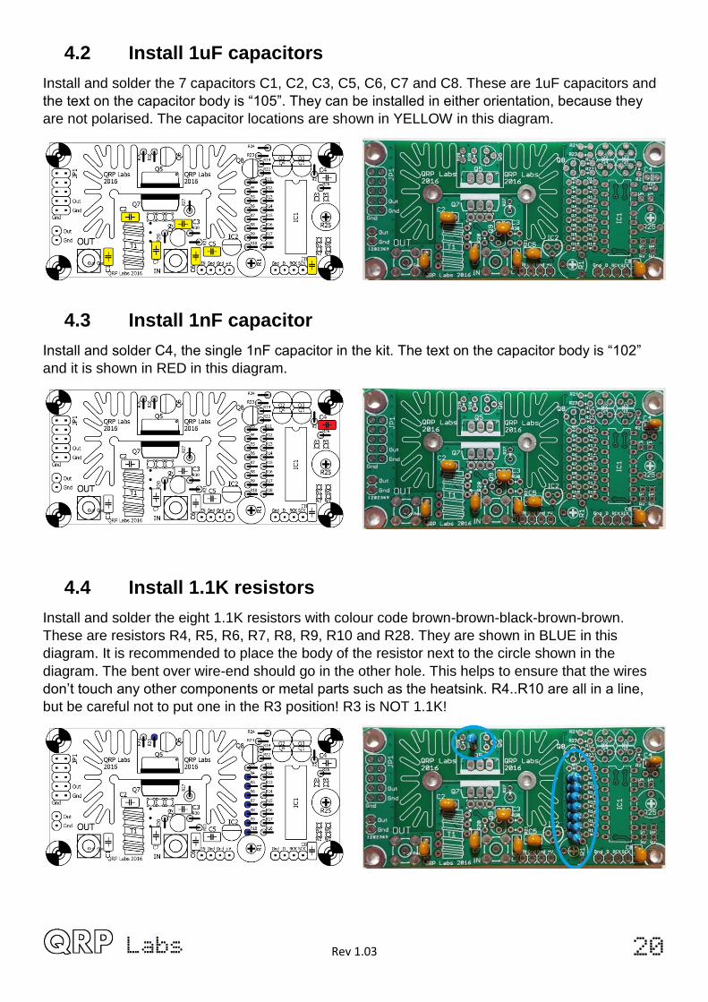
4.2 Install 1uF capacitors
Install and solder the 7 capacitors C1, C2, C3, C5, C6, C7 and C8. These are 1uF capacitors and
the text on the capacitor body is “105”. They can be installed in either orientation, because they
are not polarised. The capacitor locations are shown in YELLOW in this diagram.
4.3 Install 1nF capacitor
Install and solder C4, the single 1nF capacitor in the kit. The text on the capacitor body is “102”
and it is shown in RED in this diagram.
4.4 Install 1.1K resistors
Install and solder the eight 1.1K resistors with colour code brown-brown-black-brown-brown.
These are resistors R4, R5, R6, R7, R8, R9, R10 and R28. They are shown in BLUE in this
diagram. It is recommended to place the body of the resistor next to the circle shown in the
diagram. The bent over wire-end should go in the other hole. This helps to ensure that the wires
don’t touch any other components or metal parts such as the heatsink. R4..R10 are all in a line,
but be careful not to put one in the R3 position! R3 is NOT 1.1K!

Rev 1.03 21
4.5 Install 2.2K resistors
Install and solder the ten 2.2K resistors with colour code red-red-black-brown-brown. These are
resistors R3, R11, R12, R13, R14, R15, R16, R17, R18 and R24. They are shown in GREEN in
this diagram.
4.6 Install 3.3K resistors
Install and solder the two 3.3K resistors with colour code orange-orange-black-brown-brown.
These are resistors R20 and R22. They are shown in RED in this diagram.
4.7 Install 330-ohm resistors
Install and solder the two 330-ohm resistors with colour code orange-orange-black-black-brown.
These are resistors R21 and R30. They are shown in ORANGE in this diagram.
Rev 1.03 22
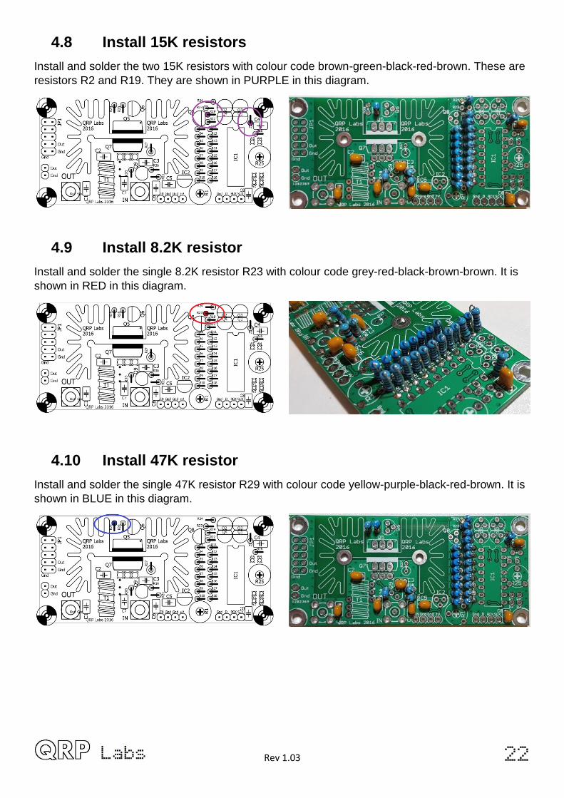
4.8 Install 15K resistors
Install and solder the two 15K resistors with colour code brown-green-black-red-brown. These are
resistors R2 and R19. They are shown in PURPLE in this diagram.
4.9 Install 8.2K resistor
Install and solder the single 8.2K resistor R23 with colour code grey-red-black-brown-brown. It is
shown in RED in this diagram.
4.10 Install 47K resistor
Install and solder the single 47K resistor R29 with colour code yellow-purple-black-red-brown. It is
shown in BLUE in this diagram.

Rev 1.03 23
4.11 Install 0.33-ohm 2W power resistor
Install and solder the single 0.33-ohm power resistor R27 with colour code orange-orange-silver-
gold. It is shown in YELLOW in this diagram.
4.12 Install 4.7K preset potentiometer
Install and solder the 4.7K preset potentiometer R1, as shown in GREEN in this diagram. Be
careful to install it in the R1 position, NOT the R25 position!
4.13 Install 78L05 voltage regulator
Install and solder the 78L05 voltage regulator IC2, as shown in RED in this diagram. Carefully
align the component shape to the drawing on the PCB silkscreen. Take care not to mix it up with
the other devices in TO92 packages which look similar! It is very difficult to correct such a mistake
later!
Rev 1.03 24
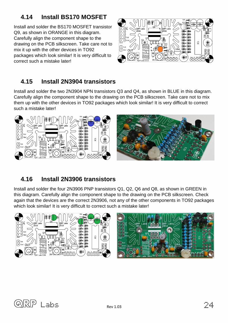
4.14 Install BS170 MOSFET
Install and solder the BS170 MOSFET transistor
Q9, as shown in ORANGE in this diagram.
Carefully align the component shape to the
drawing on the PCB silkscreen. Take care not to
mix it up with the other devices in TO92
packages which look similar! It is very difficult to
correct such a mistake later!
4.15 Install 2N3904 transistors
Install and solder the two 2N3904 NPN transistors Q3 and Q4, as shown in BLUE in this diagram.
Carefully align the component shape to the drawing on the PCB silkscreen. Take care not to mix
them up with the other devices in TO92 packages which look similar! It is very difficult to correct
such a mistake later!
4.16 Install 2N3906 transistors
Install and solder the four 2N3906 PNP transistors Q1, Q2, Q6 and Q8, as shown in GREEN in
this diagram. Carefully align the component shape to the drawing on the PCB silkscreen. Check
again that the devices are the correct 2N3906, not any of the other components in TO92 packages
which look similar! It is very difficult to correct such a mistake later!

Rev 1.03 25
4.17 Install IC1 socket
Install IC1’s socket, taking care to align the dimple on the socket with the dimple on the PCB
silkscreen drawing. Later IC1 (74HC595) will be inserted in the socket with its dimple aligned also.
4.18 Install jumper wire
Install a jumper wire connecting holes W0 and W1, as shown in the diagram below (left). This is
the standard configuration, when using the 74HC595 IC1 shift register to control the envelope-
shaping DAC, controlled by an Ultimate3S, for example. If you want to use the standalone
configuration please refer to App Note AN005. You can use a resistor wire off-cut for the jumper
wire. I recommend fitting a small loop as shown in the photo (right), so that if you later want to
remove it to change the configuration, it is easy to cut or remove.
4.19 Install headers
The kit is supplied with a single 10-pin header. If you wish, you may break it into three pieces with
2, 4 and 4 pins and install them as shown in orange in this diagram. Many people find it easier to
solder connection wires to pins rather than fit them in the small holes; or you may wish to use
connecting headers.

Rev 1.03 26
4.20 Install trifilar transformer
The trifilar transformer is installed in the position coloured red in this diagram. The photo (right)
shows the board after installing the trifilar transformer. But it is a tricky part of the assembly, so
please read and follow these steps carefully.
Firstly, the wire. The best way to un-wind it, without tangling it
up, is to think of what the kit-packing person that wound it up
did. Then reverse his steps. So, first unwind the tightly wrapped
part in the middle where the end of the wire has been secured.
Then, open out the spool of wire so that it is a circle. Then
unwind the spool, around your fingers, reversing the process of
winding it in the first place.
When you have unwound the wire and straightened it, cut it into
three approximately equal pieces. These three pieces now need to be tightly twisted together to
make the trifilar wire. My method for this is to tie one end in a knot around a small screwdriver
shaft. Similarly tie the other end around another small screwdriver. Now clamp one end somehow
to something solid. You could use a vice, if you have one. If you don’t, then you have to get
creative and think of something. Here I taped it to the edge of the desk. Now you can twist the
screwdriver at the free end, repeatedly until you twist the three wires together thoroughly. You
need to keep the wire under a little tension to keep the twists evenly spaced.

Rev 1.03 27
I put about 70-90 twists into a 25cm
length of wire. The end result is
something like the photos (right).
(The measurement scale is in cm).
Now cut off the untidy ends, and
this is the piece of wire that will be
used to wind the FT50-43 toroidal
core as a trifilar transformer.
Hold the core between thumb and finger. Pass the wire first from above, to below. Then take the
wire from below, and bring it around to pass through the toroid again to form the second turn. After
each turn, ensure the wire is fitting snugly around the toroidal core. Wind 10 turns on the core.
Each time through the toroid’s central hole counts as one turn. Cut off the excess wire, leaving
about 2.5cm remaining.

Rev 1.03 28
Now it’s necessary to identify which wire belongs to which winding.
You have three windings twisted together, they all use the same wire.
The only way to do this is with a DVM as continuity tester. First,
untwist and straighten the wire ends that are not wound around the
toroidal core.
Now tin the last few mm at the ends of each wire. You can do this by
scraping off the enamel then tinning with the soldering iron; or, hold
the wire end in a blob of molten solder for a few (maybe 10) seconds,
until the enamel burns off.
Now use a DVM to test for
continuity. Re-arrange the wires
so that there is continuity from
A-A, B-B, and C-C in this photo.
Carefully keep this orientation of
wires and insert the transformer
this way into the PCB. You can
carefully cut off those few mm of
tinned section of wire, if it won’t
fit through the PCB holes. But
BE CAREFUL not to lose the
orientation of the wires! The
right wires must be in the right
holes, so that the windings are connected correctly in the circuit!
It’s a good idea to check for continuity A-A, B-B, C-C again with the DVM, just to make sure that
you didn’t accidentally mix up the wire orientation while inserting the wires.

Rev 1.03 29
Now trim the wires underneath the board, and
tin the ends again. The EASIEST way to do this
is simply apply solder so that it sits in the hole
and surrounds the 1mm of wire ending, and hold
the soldering iron in that position for a few
seconds until the enamel is burnt away. This tins
the wires and solders them to the PCB pads.
You can inspect the joints with a magnifying
glass or jeweller’s loupe. The photograph (right)
shows a joint where the soldering iron has not
been held long enough on the joint. The enamel has not properly burnt off the wire, and there will
be no electrical connection to the copper wire. The circuit will not work! So fix it!
You can also test that the wires are properly soldered. Use a DVM to check for continuity (zero
ohms resistance) between the indicated points C and A in this diagram and photo. If there is
continuity it means that the copper wire is all properly soldered. If not, then go back and check
again. You can then check the individual windings to see where the fault lies.

Rev 1.03 30
Note that this does NOT necessarily check that you correctly orientated the windings. The only
way to do that, was with the DVM continuity check before inserting the transformer; and after
identifying the windings, being careful not to mix the wires again while inserting the transformer in
the PCB; finally checking again once the wires are inserted but before soldering.
4.21 Install heatsink assembly
In this kit both the TO220 power
transistors, the 2SC4242 (Q5) in
the power modulator and the
IRF510 final (Q7) are fitted to the
same heatsink. The metal tabs of
these transistors must not short to
ground or to other parts of the
circuit. Therefore insulating
silicone rubber pads are used,
and insulating white plastic
washers. In this photo (right) the
heatsink is viewed side-on before
assembly. The picture shows how
the transistor assembly must be
put together before soldering.
On each side of the heatsink, the silicone
pad is placed on the heatsink where the
transistor will sit. The transistor is placed
on the silicone pad. The white nylon
insulating washer is pushed into the hole
in the TO220 transistor tab. The bolt then
fits through the hole. The metal bolt does
not touch the metal tab of the transistor,
and the tab does not touch the heatsink.
The IRF510 should be installed on the
side of the heatsink with the “large gap”,
and the 2SC4242 should be installed on
the side of the transistor with the “small
gap”. In the prototypes I put the bolt on
the 2SC4242 side and the nut on the IRF510 side, as shown. Then it is easiest to grab the bolt
with pliers while tightening the screw from the other side.
If you have some heatsink compound then this would be a good idea (though the prototypes
development and testing did not use it). Take care to align the transistors accurately and tighten
the bolt/nut well. You will be rewarded by an assembly which fits easily into the holes on the PCB.

Rev 1.03 31
It is difficult to remove and replace transistors
later! So before soldering, check once again that
the Q5 transistor (2SC4242) is in the correct
place on the side of the narrow opening of the
heatsink, and the Q7 transistor (IRF510) is in the
correct place on the side of the wide opening of
the heatsink. Check that everything matches the
PCB silkscreen and this diagram (right).
Once the heatsink assembly and transistors are fitting perfectly into the PCB, you can solder first
the heatsink mounting pins, then the transistor component leads themselves. A high wattage
soldering iron may be needed for soldering the heatsink pins, as the heatsink will try to conduct
away heat which may lower the temperature of the joint below the melting point of solder. You
could leave the heatsink pins unsoldered if it seems troublesome. After soldering the transistor
leads, cut off the excess lead length.
Note that the pads for the heatsink mounting pins are not connected to ground (or anything else).
The PCB top side has no copper or tracks of any sort under the heatsink; this is to ensure that
even if the soldermask accidentally got scratched, there would be no contact between the heatsink
and ground or any other electrical connection.
4.22 A recommended modification
This modification will be included as
standard on any future PCB revisions. It
involves the addition of a 10-ohm resistor
at the gate of Q7, the IRF510 final PA
transistor. The PA does work without this
resistor, and indeed it will produce slightly
higher power output. However at certain
supply voltages and frequencies, instability
can occur. When this happens the amplifier
superimposes a low frequency oscillation
envelope on the wanted RF output. Fitting
this 10-ohm resistor resolves this potential
problem, at the cost of some power
reduction. The measurements made later
in this document were made with this 10-
ohm resistor fitted.
The modification involves cutting one track
on the BOTTOM side of the PCB, and
soldering a 10-ohm resistor on the bottom side of the PCB. The resistor location is shown in the
above circuit diagram fragment which shows the IRF510 PA. The 10-ohm resistor is supplied in
the kit and has colour code brown-black-black-silver-brown.

Rev 1.03 32
The modification is illustrated in the following diagram and picture.

Rev 1.03 33
4.23 RD15HVF1 Substitution for VHF operation
The supplied IRF510 transistor works well at HF. However for the VHF bands 6m and above, the
gain of the IRF510 in this circuit is very low. If you wish you may substitute the RD15HVF1
transistor or one of its close relatives. These transistors are more expensive but are designed for
VHF/UHF power amplifiers and should work well in this circuit.
The pinout of the RD15HVF1 is different to the IRF510! The PCB has a position for the
RD15HVF1 transistor if you
wish to use it. If you wish to use
the RD15HVF1 in this circuit,
insert its leads into the set of
three holes shown in RED in the
diagram. You will need to bend
the leads of the transistor
outwards slightly, away from the
heatsink, so that they are
aligned with this set of holes.
Take care to insert the transistor
leads into the correct holes.
5. Connecting and configuring the Power Amplifier kit
5.1 Basic connections
The power amplifier kit requires a supply voltage of typically 12 or 13.8V. The amplifier may draw
1 or 1.5A of current so remember to use a well-regulated good quality power supply capable of
this. Use thick wires to the PA to avoid voltage drop in the wiring. You may wish to connect an
electrolytic capacitor close to the PA kit PCB, particularly if the wires to your supply are long.
The RF input to the amplifier may be connected at the pin header, or you may install an SMA
connector for it. If using the pin header, it is a good idea to use a ground connection wire as well
as the RF signal connection wire. Thin coax is suitable.
The RF output may be taken from a pin header, or an SMA connector, or the 2 x 5-pin header
pads provided. The footprint for the 2 x 5-pin header is provided to facilitate connection to the
Ultimate3S kit – if you are using this then please refer to App Note AN004. As usual, remember to
connect a low pass filter at the PA output, to attenuate transmitter harmonics.
The 4-pin header on the below right of the diagram connects the PA to a microcontroller. The
microcontroller should load in a sequence of numbers to the shift register to cause the RF
envelope to have a raised cosine shape. App Note AN004 describes how to connect these signals
to the Ultimate3S transmitter kit, if you wish to use that as the driver.
An alternative is to replace IC1 with an ATtiny84 microcontroller that generates the raised cosine
RF envelope profile; this is described in App Note AN005.

Rev 1.03 34
5.2 Bias adjustment
Correct bias adjustment is very important! Before
connecting power, turn the R1 bias potentiometer
completely anti-clockwise (zero volts bias)!
R1 adjusts the bias at the gate of the IRF510 final PA
transistor Q7. If the bias is too low, the gain (and power
output) of the amplifier will be low. If the bias is too high,
the current through Q7 will flow even when there is no
signal; this can result in excess power dissipation (though
the power modulator circuit removes power to the IRF510
PA final in any case). Efficiency is also reduced and
gain/power output may be reduced also if bias is too high.
Theoretically the ideal bias point for the gate of the MOSFET, is where there is zero idle current
through the IRF510 transistor, and where increasing the bias voltage any further would result in
idle current starting to flow. This point has optimal power output, if the input signal amplitude is
optimum, and it has best efficiency as well as spectral purity of the output. Of course in the real
world, everything can (and does) change!

Rev 1.03 35
The zero idle current point can be found quite
easily if you connect an ammeter (typically a
DVM in current measurement mode) in series
with the PA kit supply. The adjustment is carried
out in the key-up state, or in other words, no RF
input (you could disconnect the RF input, for
example).
To do this, you will need to force the power
modulator circuit to apply voltage to the PA
transistor. In other words, the DAC should be
loaded with 255 to force the power modulator to
maximum voltage. Another way to do this is to temporarily connect a wire from the DAC output to
+5V. You can do this by connecting a short wire offcut from the left end of R26, to the W4 pad on
the PCB (as shown). Remember to remove this wire later!
Start with R1 completely anti-clockwise. Observe the current consumption of the PA kit when “idle”
(key-up state, not transmitting, no RF input). Then slowly turn the R1 trimmer potentiometer
clockwise until you observe a very slight increase in the current consumption. The point where the
current just starts to increase is the zero bias point.
An alternative (and arguably simpler) method of bias adjustment is to transmit into a 50-ohm
dummy load, measuring power with a power meter or observing on an oscilloscope. Turn the R1
trimmer potentiometer clockwise until maximum power output is obtained, then back off slightly.
The bias setting using this method is higher than the zero idle current method. The power output
will be higher too.
The gain of the IRF510 amplifier is less at the upper end of the HF bands particularly 28MHz (the
10m band). The input signal is also typically lower, when using for example an Ultimate3S kit as
the driver. In these cases, adjusting the PA with a higher bias voltage can improve the gain/power
output at the high frequency end of its range of operation.
If using this PA in a multi-band transmitter and desiring maximum power output, you could adjust
the bias for best power output on the highest frequency that will be used (for example, 28MHz)
where the bias is most critical. The bias setting is much less critical at the lower end of HF.
5.3 Maximum DAC value
Refer back to the theoretical explanation of the 8-bit DAC controlled power modulator in the PA kit,
which can be used to closely replicate a raised cosine shape. The output voltage range of the
DAC is 0..5V. Remember that the modulator circuit is like a power op-amp in a feedback
configuration which tries to keep its two inputs at the same voltage. The feedback ratio is set in
this case by the resistors R23 and R24 which are 8.2K and 2.2K respectively. These resistors form
a potential divider, the output voltage of the power modulator is scaled by a multiplier of 2.2 / (2.2
+ 8.2) = 0.21. In other words, a DAC value of 255, which cases a DAC output voltage of 5V
approximately, will correspond to a power modulator output voltage of 23.6V.
If using a PA supply voltage less than about 25V (remember a volts or two will be lost in the power
modulator anyway), the DAC raised cosine profile should not use the full range 0..255. For
example, consider a 12V supply. A DAC setting of 255 will try to drive the power modulator to
23.6V output but this is clearly impossible because the supply voltage is only 12V. The power
modulator saturates. What this means is that the raised cosine shape at the top of the RF

Rev 1.03 36
envelope will not be achieved. Therefore the range of the DAC should be limited to a number
lower than 255, which depends on the supply voltage used.
If using the Ultimate3S kit to drive this PA kit, the firmware (version v3.12 and above) includes a
parameter to set the DAC maximum. The firmware then applies a scaling calculation to the raised
cosine envelope profile.
This maximum DAC value to avoid saturation was determined experimentally by measurement at
different supply voltages. The results over supply voltage range 8 to 19V approx. are shown
below, with a straight line best fit drawn between them.
From the line, at 12V supply, the maximum DAC value should be 122. To compare this to the
theoretical prediction, we can calculate the expected power modulator voltage as follows:
DAC voltage = 5.0 * 122 / 255 = 2.39V
Power modulator output voltage = 2.39 / 0.21 = 11.4V
This is reasonable considering that we know some voltage drop will occur in the power modulator
itself – in other words, it does not function quite as well as a rail-to-rail op-amp.
From the equation, the maximum DAC values for 12V and 13.8V are:
• 12V maximum DAC value: 122
• 13.8V maximum DAC value: 147
In practice, lots of things may vary. Component value tolerances will make the line in this
measurement slightly different in every case. Your supply voltage may be less than the 12V or
13.8V you expect to use – many regulated supplies are not perfect, and with 1 or 1.5A current
draw you will expect to drop a small amount of voltage in the cables between the power supply
and the PA kit (which is why I recommended earlier, to use thick wires, to minimise this!). The 5V
regulated voltage in the kit itself may also not be exact.

Rev 1.03 37
Therefore to avoid saturation which will distort the top of the raised cosine envelope, and if you
wish to use the equation rather than make extensive measurements of your own, then I
recommend reducing those DAC values slightly to apply a safety margin. For example, for 12V
use a maximum DAC value of 115 and for 13.8V, use 140.
5.4 Heatsink temperature rise; PA kit installation in enclosure
The desired output power of this PA kit in your application has a significant bearing on how you
enclose the project. Remember that the heatsink will dissipate a considerable amount of heat. The
heat dissipation will cause the temperature of the heatsink to rise. You need to take this into
account when deciding what enclosure to use. You may wish to bolt the heatsink to the back of a
metal box, for example; or consider a fan to cool the heatsink.
In operation the power modulator transistor will dissipate some heat as it is an imperfect switch;
the IRF510 final PA will operate at perhaps 50% efficiency or something like that (dependent on
many factors). For a power output of 5W you will therefore be dissipating at least 5W, maybe
somewhat more.
Another factor to take into account is the transmission mode you will be using. A continuous key-
down transmission using FSK modes such as WSPR, will dissipate a much higher average power
than an on/off keyed mode such as CW.
As an example, one prototype here was
operated on continuous key-down on
10MHz, with 13.8V supply using an
Ultimate3S transmitter as the driver.
The power output was set to 5W using
the maximum DAC value (meaning
excess power was also dissipated in the
power modulator). An overall current
consumption of 1.06A was recorded.
The assembly was lying on the
workbench with no enclosure, and no
forced air cooling. It took about half an
hour for the temperature of the heatsink
to stabilise. By that time it had reached
a temperature of 61C which was a rise of 33C above the ambient temperature of the lab. The
transmission was switched off after 40 minutes (see chart).
In summary: Enclosing the PA kit in an enclosure will increase the temperature rise; using fan-
assisted cooling would reduce it. There are many factors that will influence heat dissipation. The
above discussion should be taken as a guideline only – your mileage may (WILL) vary!
5.5 Modifications for higher power output
If you really want to get as much power output from this PA as possible, then you can experiment
with the following component values. I’m not really recommending it as such, I’m just providing the
following discussion points because there are undoubtedly some people who crave POWER.

Rev 1.03 38
As an example, during development I was able to obtain 30W power output on the 30m band
(10MHz) using a 30V supply. But to do this, you will need to take care, be prepared to experiment,
be prepared to modify component values, and not get upset if you fry one or more components
(particularly IRF510).
The overriding principle here is that in order to get more power output, you need a higher supply
voltage. 12V or 13.8V supplies are recommended for this kit but if you want higher power, and are
prepared to experiment, then you can go higher than this.
There’s a lot to experiment with, learn and explore, if you are inclined to do this with your PA kit.
The following sections for the experienced constructor, discuss some of the factors you may take
into consideration when experimenting with increased power output.
5.5.1 Abandon the DAC-controlled power modulator
The 8-bit DAC controlled power modulator allows a microcontroller to generate a precise raised
cosine envelope shape. However, it cannot be denied that there is also some voltage drop across
the power modulator transistor Q5, as well as the 0.33-ohm current limiting resistor R27.
Bypassing these components will allow the full supply voltage to reach the PA transistor, resulting
in maximum power output. You will lose the raised cosine envelope shape. That may or may not
be a problem, for your application. The raised cosine envelope is really most applicable to on/off
keyed modes. FSK modes are less troubled by key clicks, except when the transmission starts
and finishes.
5.5.2 Remove the leakage gate
The leakage gate discussed in section 3.5 reduces the leakage through the PA on key-up. But it
also slightly attenuates the drive to the IRF510 PA transistor (Q7) gate, which reduces the gain of
the amplifier (and final power output). If you don’t care about this leakage, or if your driver stage is
also keyed, then bypassing this leakage gate will slightly increase power output.
5.5.3 Increase the DAC scaling so that it can control higher supply voltages
Assuming that you DO still want to use the DAC-controlled power modulator for raised-cosine key
shaping, then the potential divider formed by R23/R24 can be adjusted to allow a greater voltage
control range. Section 5.3 above explained the maximum DAC value. With the supplied
components the DAC cannot theoretically control a range of more than 0..23.6V. To increase the
upper voltage limit, the resistor R23 should be increased. For example, changing R23 from 8.2K to
15K increases the control range to 0..39V.
5.5.4 Take care of the 78L05 voltage regulator
The 78L05 voltage regulator IC2 has a maximum input voltage rating of 35V. In my experience if
you exceed this, it simply shuts down. If you intend to exceed 35V supply, and retain the DAC-
controlled power modulator, then you will need to arrange for a 5V supply in another way.
Rev 1.03 39
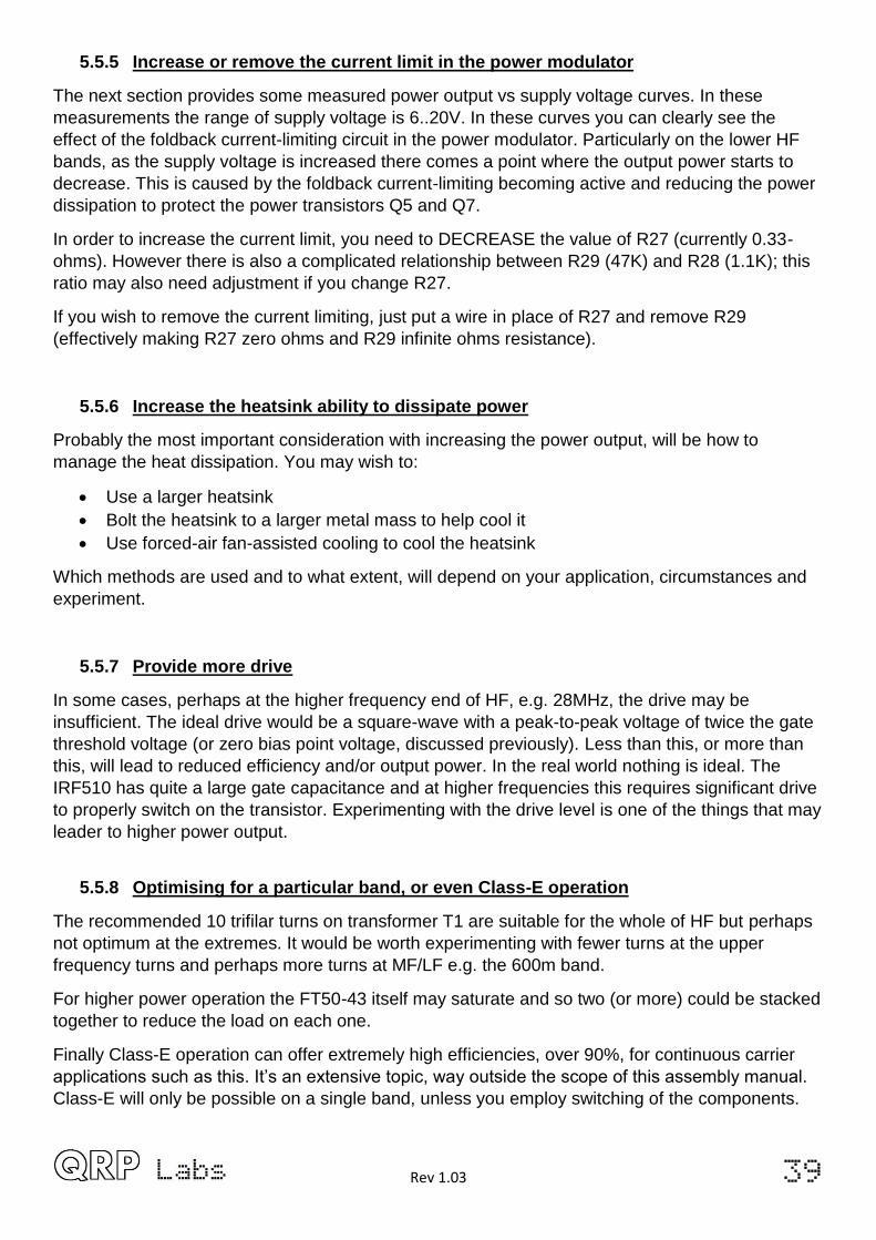
5.5.5 Increase or remove the current limit in the power modulator
The next section provides some measured power output vs supply voltage curves. In these
measurements the range of supply voltage is 6..20V. In these curves you can clearly see the
effect of the foldback current-limiting circuit in the power modulator. Particularly on the lower HF
bands, as the supply voltage is increased there comes a point where the output power starts to
decrease. This is caused by the foldback current-limiting becoming active and reducing the power
dissipation to protect the power transistors Q5 and Q7.
In order to increase the current limit, you need to DECREASE the value of R27 (currently 0.33-
ohms). However there is also a complicated relationship between R29 (47K) and R28 (1.1K); this
ratio may also need adjustment if you change R27.
If you wish to remove the current limiting, just put a wire in place of R27 and remove R29
(effectively making R27 zero ohms and R29 infinite ohms resistance).
5.5.6 Increase the heatsink ability to dissipate power
Probably the most important consideration with increasing the power output, will be how to
manage the heat dissipation. You may wish to:
• Use a larger heatsink
• Bolt the heatsink to a larger metal mass to help cool it
• Use forced-air fan-assisted cooling to cool the heatsink
Which methods are used and to what extent, will depend on your application, circumstances and
experiment.
5.5.7 Provide more drive
In some cases, perhaps at the higher frequency end of HF, e.g. 28MHz, the drive may be
insufficient. The ideal drive would be a square-wave with a peak-to-peak voltage of twice the gate
threshold voltage (or zero bias point voltage, discussed previously). Less than this, or more than
this, will lead to reduced efficiency and/or output power. In the real world nothing is ideal. The
IRF510 has quite a large gate capacitance and at higher frequencies this requires significant drive
to properly switch on the transistor. Experimenting with the drive level is one of the things that may
leader to higher power output.
5.5.8 Optimising for a particular band, or even Class-E operation
The recommended 10 trifilar turns on transformer T1 are suitable for the whole of HF but perhaps
not optimum at the extremes. It would be worth experimenting with fewer turns at the upper
frequency turns and perhaps more turns at MF/LF e.g. the 600m band.
For higher power operation the FT50-43 itself may saturate and so two (or more) could be stacked
together to reduce the load on each one.
Finally Class-E operation can offer extremely high efficiencies, over 90%, for continuous carrier
applications such as this. It’s an extensive topic, way outside the scope of this assembly manual.
Class-E will only be possible on a single band, unless you employ switching of the components.

Rev 1.03 40
6. Power Amplifier characteristics
These measurements were made using a QRP Labs Ultimate3S transmitter kit as driver, with a
single BS170 transistor running at 5V supply. The curves show the Power Amplifier kit with 12V
and 13.8V supply voltage. The output of the PA kit was connected to a QRP Labs Low Pass Filter
Kit, whose output was connected to a QRP Labs 50-ohm 20W Dummy Load kit. Measurements
were made on 600m, 160m, 80m, 40m, 30m, 20m, 15m and 10m bands (frequencies 0.5, 2, 3.5,
7, 10, 14, 21 and 28MHz respectively).
Power measurements were made with a 100MHz Digital Storage Oscilloscope using the peak-
peak measurement facility, and a 50-ohm coax with BNC connectors directly connecting the LPF
output to the oscilloscope input. The supply voltage measurement was made at the PCB itself to
eliminate any potential losses due to high currents on cables between the power supply and the
PA kit. The measurement was made using the second channel on the Digital Storage Oscilloscope
and a calibrated x10 probe.
These measurements show four different conditions. There are adjustments to the bias voltage of
both the driver (Ultimate3S) and the PA kit IRF510. Both single-winding and bifilar transformer in
the drain circuit of the Ultimate3S driver were tried.
In practice, do not expect to replicate these measurements precisely. You may measure more, or
less, power than has been measured here. It is notoriously difficult to measure power accurately.
Many factors come into this, such as:
• Measurement equipment accuracy and calibration
• RF ground loops and related cabling effects
• Physical layout of the modules
• Every LPF is constructed differently, with component tolerances having a big effect, as well
as inductor winding style – unless the LPF is constructed with inductance measurement
instruments to check the values
• Component tolerances in the PA kit itself
So power measurements always need to be taken with a pinch of salt. Do not worry if you do not
exactly match the results presented here, or your own expectations. The measurements here were
taken on an assembled PA kit from the final kit manufacturing run. It is therefore an identical kit to
the one you are constructing now. The results are presented as an indication of what to expect.

Rev 1.03 41
6.1 Output power vs Frequency
The first two charts show a single winding L1 inductor in the Ultimate3S transmitter. Left: the driver
bias and PA bias were re-adjusted each time the band was changed, to obtain best power output.
Right: The driver and PA bias adjustment is for zero idle current. To perform this adjustment, the
trimmer potentiometer is first set anti-clockwise (0V bias), with the transmitter off (key-up), i.e. no
input signal. A DVM is used to measure the current consumption of the Ultimate3S / PA
(depending on which bias is being adjusted). The trimmer is slowly turned clockwise until a very
slight increase in idle current (key-up current) can be seen.
This second set of measurements uses a bifilar transformer in the Ultimate3S driver – which is the
subject of an article on QRP Labs website (see references). Left: with zero idle current bias (see
above). Right: the bias is adjusted for maximum power output on 10m band.
Conclusions may be drawn from these measurements, about the best way to adjust your PA kit.
1) An easy and safe way to adjust the kit is the zero idle current method (explained above).
However higher output power is obtainable on the higher frequency bands, particularly 10m
and 15m, by adjusting for a positive idle current. Highest frequency operation is most
critical. A good method will be to adjust for the highest output power on the highest
intended frequency of operation.
2) There is no advantage to the use of a bifilar transformer in the Ultimate3S when it is used
as the driver stage. For highest power output, use a single winding inductor in the drain
circuit of the Ultimate3S driver.
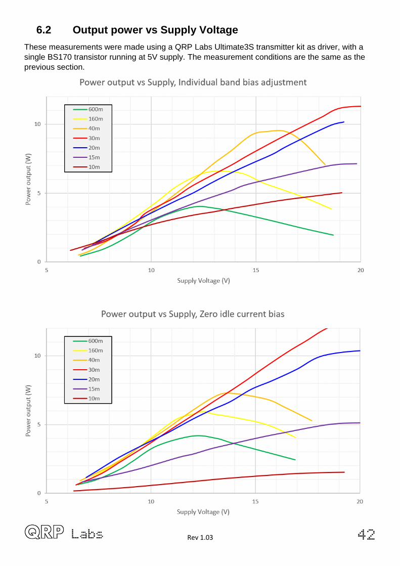
Rev 1.03 42
6.2 Output power vs Supply Voltage
These measurements were made using a QRP Labs Ultimate3S transmitter kit as driver, with a
single BS170 transistor running at 5V supply. The measurement conditions are the same as the
previous section.

Rev 1.03 43

Rev 1.03 44
7 References
• App Note AN004 explains how to use this PA kit in conjunction with an Ultimate3S
QRSS/WSPR kit to increase the output power to around 5W, and apply raised cosine RF
envelope shaping for a beautiful clean click-free signal. Refer to http://qrp-
labs.com/appnotes
• App Note AN005 explains how to replace IC1 with a programmed ATtiny84 chip from QRP
Labs which takes care of the raised cosine envelope profile for using the PA kit in a
standalone configuration (without an external microcontroller loading the raised cosine
coefficients into the 8-bit shift register that feeds the DAC). Refer to http://qrp-
labs.com/appnotes
• For updates relating to this kit please visit the QRP Labs PA Kit page http://qrp-labs.com/pa
• For any questions regarding the assembly and operation of this kit please join the QRP
Labs group, see http://qrp-labs.com/group for details
8 Document Revision History
1.0 29-Dec-2016 Initial revision
1.01 04-Jan-2017 Corrected typo in section 3.1
1.02 09-Mar-2017 Corrected typo in the toroid part name in several places
1.03 29-Nov-2018 Corrected BS170 in parts list, it is TO92 not TO220 package
Related Documents