A3R1GE30JBF A3R1GE40JBF 1Gb DDRII Synchronous DRAM Revision 1.5 Nov., 2017 1Gb DDRII SDRAM Specification A3R1GE30JBF A3R1GE40JBF Zentel Electronics Corp.

Welcome message from author
This document is posted to help you gain knowledge. Please leave a comment to let me know what you think about it! Share it to your friends and learn new things together.
Transcript

A3R1GE30JBF A3R1GE40JBF
1Gb DDRII Synchronous DRAM
Revision 1.5 Nov., 2017
1Gb DDRII SDRAM Specification
A3R1GE30JBF
A3R1GE40JBF
Zentel Electronics Corp.

A3R1GE30JBF A3R1GE40JBF
1Gb DDRII Synchronous DRAM
Revision 1.5 Nov., 2017
Page 1 / 72
Zentel Electronics Corporation reserve the right to change products or specification without notice.
Specifications Features
Density: 1G bits
Organization
16M words 8 bits 8 banks (A3R1GE30JBF)
8M words 16 bits 8 banks (A3R1GE40JBF)
Package
60-ball FBGA(μ BGA) (A3R1GE30JBF)
84-ball FBGA(μ BGA) (A3R1GE40JBF)
Lead-free (RoHS compliant)
Power supply: VDD, VDDQ 1.8V 0.1V
Data rate: 1066Mbps/800Mbps (max.)
1KB page size (A3R1GE30JBF)
Row address: A0 to A13
Column address: A0 to A9
2KB page size (A3R1GE40JBF)
Row address: A0 to A12
Column address: A0 to A9
Eight internal banks for concurrent operation
Interface: SSTL_18
Burst lengths (BL): 4, 8
Burst type (BT):
Sequential (4, 8)
Interleave (4, 8)
/CAS Latency (CL): 3, 4, 5, 6, 7
Recharge: auto recharge option for each burst access
Driver strength: normal/weak
Low self-refresh current (IDD6) parts are available
Refresh: auto-refresh, self-refresh
Refresh cycles: 8192 cycles/64ms
Average refresh period at different temperature range
7.8s at TC ≤ 85C
3.9s at +85C < TC ≤ +95C
1.95us at +95C < TC ≤ +105C
Automotive grade 3 compliant with AEC-Q100 grade 3
Automotive grade 2 compliant with AEC-Q100 grade 2
Operating case temperature range
TC = 0C to 85C (Commercial)*
TC = -40°C to 95°C (Industrial)*
TC = -40°C to 95°C (Automotive grade 3 )*
TC = -40°C to 105°C (Automotive grade 2)*
Note: Refer to operating temperature condition on page 5 for
details
Double-data-rate architecture; two data transfers per clock cycle
The high-speed data transfer is realized by the 4 bits prefetch pipelined architecture
Bi-directional differential data strobe (DQS and /DQS) is transmitted/received with data for capturing data at the receiver
DQS is edge-aligned with data for READs; center- aligned with data for WRITEs
Differential clock inputs (CK and /CK)
DLL aligns DQ and DQS transitions with CK transitions
Commands entered on each positive CK edge; data and data mask referenced to both edges of DQS
Data mask (DM) for write data
Posted /CAS by programmable additive latency for better command and data bus efficiency
On-Die-Termination for better signal quality
Programmable RDQS, /RDQS output for making 8
organization compatible to 4 organization
/DQS, (/RDQS) can be disabled for single-ended Data Strobe operation
Off-Chip Driver (OCD) impedance adjustment is not supported

A3R1GE30JBF A3R1GE40JBF
1Gb DDRII Synchronous DRAM
Revision 1.5 Nov., 2017
Page 2 / 72
Ordering Information
Organization Internal Speed bin
Part number (words × bits) Banks (CL-tRCD-tRP) Package Note
A3R1GE30JBF-AH/AHI/AHB/AHA 128M × 8 8
DDR2-1066 (7-7-7) 60-ball FBGA
A3R1GE30JBF-8E/8EI/8EB/8EA DDR2-800 (5-5-5)
A3R1GE40JBF-AH/AHI/AHB/AHA 64M × 16 8
DDR2-1066 (7-7-7) 84-ball FBGA
A3R1GE40JBF-8E/8EI/8EB/8EA DDR2-800 (5-5-5)
A3R1GE40JBF-8EPH 64M × 16 8 DDR2-800 (5-5-5) 84-ball FBGA
Low IDD6 A3R1GE40JBF-8EJ 64M × 16 8 DDR2-800 (5-5-5) 84-ball FBGA
A3R1GE30JBF-8EJ 128M × 8 8 DDR2-800 (5-5-5) 60-ball FBGA
Part Number
A 3 R 1G E 4 0J BF - 8E PH
Blank: I: B: A: PH: J:
Commercial Industrial Automotive grade 3 Automotive grade 2 Commercial Industrial
normal IDD6 normal IDD6 normal IDD6 normal IDD6 low IDD6 low IDD6
Option
Speed
8E: DDR2-800 AH: DDR2-1066
Package Type BF: FBGA
Die version 0J: Version 0J
IO Configuration
3: x8 4: x16
Classification E: DDR2
Density 1G: 1Gbits
Interface R: SSTL-18
Product line 3: DRAM
Zentel memory

A3R1GE30JBF A3R1GE40JBF
1Gb DDRII Synchronous DRAM
Revision 1.5 Nov., 2017
Page 3 / 72
Pin Configurations
/xxx indicates active low signal.
Pin name Function Pin name Function
A0 to A13 Address inputs ODT ODT control
BA0, BA1,BA2 Bank select VDD Power Supply
DQ0 to DQ15 Data input/output VSS Ground
DQS,/DQS UDQS, /UDQS Differential data strobe VDDQ Power Supply for DQ circuit LDQS, /LDQS
RDQS,/RDQS Differential data strobe for read VSSQ Ground for DQ circuit
/CS Chip select VREF Input reference voltage
/RAS,/CAS,/WE Command input VDDL Power Supply for DLL circuit
CKE Clock enable VSSDL Ground for DLL circuit
CK,/CK Differential clock input NC*1
No connection
DM Write data mask NU
*2 Not usable
UDM, LDM
Notes: 1. Not internally connected with die.
2. Don’t use other than reserved functions.

A3R1GE30JBF A3R1GE40JBF
1Gb DDRII Synchronous DRAM
Revision 1.5 Nov., 2017
Page 4 / 72
CONTENTS
Specifications ...................................................................................................................... 1
Features ............................................................................................................................. 1
Ordering Information ............................................................................................................ 2
Part Number ....................................................................................................................... 2
Pin Configurations ............................................................................................................... 3
Electrical Specifications ....................................................................................................... 5
Block Diagram..................................................................................................................... 24
Pin Function ........................................................................................................................ 25
Command Operation ........................................................................................................... 27
Simplified State Diagram ...................................................................................................... 35
Operation of DDR2 SDRAM ................................................................................................. 36
Package Drawing ................................................................................................................ 70
Recommended Soldering Conditions .................................................................................... 72

A3R1GE30JBF A3R1GE40JBF
1Gb DDRII Synchronous DRAM
Revision 1.5 Nov., 2017
Page 5 / 72
Electrical Specifications
All voltages are referenced to VSS (GND)
Execute power-up and Initialization sequence before proper device operation is achieved
Absolute Maximum Ratings
Parameter Symbol Rating Unit Note
Power supply voltage VDD -1.0 to +2.3 V 1
Power supply voltage for output VDDQ -0.5 to +2.3 V 1
Power supply voltage for DLL VDDL -0.5 to +2.3 V 1
Input voltage VIN -0.5 to +2.3 V 1
Output voltage VOUT -0.5 to +2.3 V 1
Storage temperature Tstg - 55 to +150 °C 1,2
Power dissipation PD 1.0 W 1 Notes: 1.Stresses greater than those listed under Absolute Maximum ratings may cause permanent damage to the device.
This is a stress rating only and functional operation of the device at these or any other conditions above those indicated in the operational sections of this specification is not implied. Exposure to absolute maximum rating conditions for extended periods may affect reliability.
2. Storage temperature is the case surface temperature on the center/top side of the DRAM.
Caution
Exposing the device to stress above those listed in Absolute Maximum Ratings could cause permanent damage. The device is not meant to be operated under conditions outside the limits described in the operational section of this specification. Exposure to Absolute Maximum Rating conditions for extended periods may affect device reliability.
Operating temperature condition
Product grades Parameter Symbol Rating Unit Note
Commercial
Operating case temperature
TC 0 to + 85 °C 1, 2, 3, 4
Industrial TC -40 to + 95 °C 1, 3, 4
Automotive grade 3 TC -40 to + 95 °C 1, 3, 4
Automotive grade 2 TC -40 to + 105 °C 1, 3
Notes : 1. Operating temperature is the case surface temperature on the center/top side of the DRAM.
2. Supporting 0 to +85C with full AC and DC specifications.
3. Supporting up to +85C and being able to extend to +95C or +105C (Automotive grade 2 only)
with doubling auto-refresh commands in frequency to a 32ms period (tREFI = 3.9μs) and higher
temperature Self-Refresh entry via A7 “1” on EMRS (2).
4. Supporting up to 105C with 4 times auto-refresh commands in frequency to a 16ms period
(tREFI=1.95us), do not use burst-refresh and do not use self-refresh mode

A3R1GE30JBF A3R1GE40JBF
1Gb DDRII Synchronous DRAM
Revision 1.5 Nov., 2017
Page 6 / 72
Recommended DC Operating Conditions (SSTL_18) Parameter Symbol min. typ. max. Unit Note
Power Supply voltage VDD 1.7 1.8 1.9 V 4
Power Supply voltage for output VDDQ 1.7 1.8 1.9 V 4
Power Supply voltage for DLL VDDL 1.7 1.8 1.9 V 4
Input reference voltage VREF 0.49 x VDDQ 0.50 x VDDQ 0.51 x VDDQ V 1.2
Termination voltage VTT VREF - 0.04 VREF VREF + 0.04 V 3
DC input logic high VIH (DC) VREF + 0.125 - VDDQ + 0.3 V
DC input logic low VIL (DC) -0.3 - VREF - 0.125 V
AC input logic high -AH, -8E
VIH (AC)
VREF + 0.200
-
-
V
AC input logic low -AH, -8E
VIL (AC)
-
-
VREF - 0.200
V
Notes: 1.The value of VREF may be selected by the user to provide optimum noise margin in the system. Typically the
value of VREF is expected to be about 0.5 x VDDQ of the transmitting device and VREF are expected to track variations in VDDQ.
2.Peak to peak AC noise on VREF may not exceed ±2% VREF (DC) 3.VTT of transmitting device must track VREF of receiving device. 4.VDDQ tracks with VDD, VDDL tracks with VDD. AC parameters are measured with VDD, VDDQ and VDDL
tied together.

A3R1GE30JBF A3R1GE40JBF
1Gb DDRII Synchronous DRAM
Revision 1.5 Nov., 2017
Page 7 / 72
AC Overshoot / Undershoot Specification
Parameter Pins Specification Unit
Maximum peak amplitude allowed for overshoot
Command, Address
0.5 V
Maximum peak amplitude allowed for undershoot
CKE, ODT 0.5 V
Maximum overshoot area above VDD
DDR2-1066 0.5 V-ns
DDR2-800 0.66 V-ns
Maximum undershoot area below VSS
DDR2-1066 0.5 V-ns
DDR2-800 0.66 V-ns
Maximum peak amplitude allowed for overshoot
CK, /CK 0.5 V
Maximum peak amplitude allowed for undershoot
0.5 V
Maximum overshoot area above VDD
DDR2-1066 0.19 V-ns
DDR2-800 0.23 V-ns
Maximum undershoot area below VSS
DDR2-1066 0.19 V-ns
DDR2-800 0.23 V-ns
Maximum peak amplitude allowed for overshoot
DQ, DQS, /DQS, 0.5 V
Maximum peak amplitude allowed for undershoot
UDQS, /UDQS, 0.5 V
Maximum overshoot area above VDD LDQS, /LDQS,
DDR2-1066 RDQS, /RDQS, 0.19 V-ns
DDR2-800 DM, UDM, LDM 0.23 V-ns
Maximum undershoot area below VSS
DDR2-1066 0.19 V-ns
DDR2-800 0.23 V-ns

A3R1GE30JBF A3R1GE40JBF
1Gb DDRII Synchronous DRAM
Revision 1.5 Nov., 2017
Page 8 / 72
DC Characteristics 1 . x8 x16
Parameter Symbol Grade max. max. Unit Test condition
Operating current (ACT- PRE)
IDD0
-AH 75 75
mA
one bank; tCK = tCK (IDD), tRC = tRC (IDD),
tRAS min. (IDD); CKE is H, /CS is H between valid commands; Address bus inputs are SWITCHING;
Data bus inputs are SWITCHING -8E 70 70
Operating current
(ACT-READ-PRE) IDD1
-AH 80 80
mA
one bank; IOUT = 0mA;
BL = 4,CL = CL(IDD), AL = 0; tCK = tCK (IDD), tRC = tRC (IDD); tRAS =tRAS min. (IDD); tRCD = tRCD (IDD);
CKE is H, /CS is H between valid commands; Address bus inputs are SWITCHING;
Data pattern is same as IDD4W
-8E 75 75
Precharge power-
down standby current IDD2P
-AH
-8E
25
20
25
20 mA
all banks idle; tCK = tCK (IDD);CKE is L; Other control and address bus inputs are STABLE;
Data bus inputs are FLOATING
Precharge quiet Standby current
IDD2Q -AH -8E
35 30
35 30
mA
all banks idle; tCK = tCK (IDD);
CKE is H, /CS is H; Other control and address bus inputs are STABLE; Data bus inputs are FLOATING
Idle standby current IDD2N -AH
-8E
40
35
40
35 mA
all banks idel tCK = tCK (IDD); CKE is H, /CS is H;
Other control and address bus inputs are SWITCHING; Data bus inputs are SWITDCHING
Active power–down
Standby current
IDD3P-F -AH -8E
45 40
45 40
mA
All banks open;
tCK = tCK (IDD); CKE is L;
Other control and address bus inputs are STABLE; Data bus input are
Floating
Fast=PDN Exit MRS(12) = 0
IDD3P-S -AH
-8E
40
35
40
35 mA
Slow PDN Exit
MRS(12) = 1
Active standby current
IDD3N
-AH 75 75
mA
all banks open;
tCK = tCK (IDD); tRAS = tRAS max. (IDD), tRP = tRP (IDD); CKE is H, /CS is H between valid commands;
Other control and address bus inputs are SWITCHING; Data bus inputs are SWITCHING
-8E 70 70
Operating current (Burst read operating)
IDD4R
-AH 165 165
mA
all banks open, continuous burst reads, IOUT = 0mA; BL = 4,CL = CL(IDD), AL = 0; tCK = tCK (IDD);
tRAS = tRAS max. (IDD), tRP = tRP (IDD); CKE is H, /CS is H between valid commands;
Address bus inputs are SWITCHING; Data pattern is same as IDD4W
-8E 135 135
Operating current
(Burst write operating) IDD4W
-AH 200 200
mA
all banks open, continuous burst writes;
BL = 4, CL = CL (IDD), AL = 0 tCK = tCK (IDD),
tRAS = tRAS max. (IDD), tRP = tRP (IDD); CKE is H, /CS is H between valid commands; Address bus inputs are SWITCHING;
Data bus inputs are SWITCHING -8E 160 160

A3R1GE30JBF A3R1GE40JBF
1Gb DDRII Synchronous DRAM
Revision 1.5 Nov., 2017
Page 9 / 72
x8 x16
Parameter Symbol Grade max. max. Unit Test condition
Auto-refresh current
IDD5
-AH 120 120
mA
tCK = tCK (IDD);
Refresh command every tRFC (IDD) interval; CKE is H, /CS is H between valid commands; Other control and address bus inputs are SWITCHING;
Data bus inputs are SWITCHING -8E 110 110
Self-refresh current IDD6
-AH,-8E 10 10
mA
Self Refresh Mode;
CK and /CK at 0V; CKE ≦ 0.2V; Other control and address bus inputs are FLOATING;
Data bus inputs are FLOATING
-8EPH - 5
-8EJ ≦85°C 5 5
>85°C 7 7
Operating current
(Bank interleaving) IDD7
-AH 185 185
mA
all bank interleaving reads, IOUT = 0mA; BL = 4, CL= CL (IDD),
AL = tRCD (IDD) – 1 × tCK (IDD); tCK = tCK (IDD), tRC = tRC (IDD),
tRRD = tRRD (IDD), tRCD = 1 x tCK (IDD) CKE is H, CS is H between valid commands; Address bus inputs are STABLE during DESELECTs;
Data pattern is same as IDD4W;
-8E 175 175
*Notes: 1. IDD specifications are tested after the device is properly initialized. 2. Input slew rate is specified by AC Input Test Condition. 3. IDD parameters are specified with ODT disabled. 4. Data bus consists of DQ, DM, DQS, /DQS, RDQS and /RDQS, IDD values must be met with all combinations of
EMRS bits 10 and 11. 5. Definitions for IDD
L is defined as VIN no greater than VIL (AC) (max.) H is defined as VIN no less than VIH (AC) (min.) STABLE is defined as inputs stable at an H or L level FLOATING is defined as inputs at VREF = VDDQ/2 SWITCHING is defined as: Inputs changing between H and L every other clock cycle (once per two clocks) for address and control signals, and inputs changing between H and L every other data transfer (once per clock) for DQ signals no including no including masks or strobes.
6. Refer to AC Timing for IDD Test Conditions.
7. When TC > 85C, IDD6 must be increased by 50% (IDD6 will increase by this amount if TC < 85C and double refresh option is still enabled)
8. For Automotive grade 2 products, when TC > 95C, IDD0-IDD5 and IDD7 must be increased by 10%
AC Timing for IDD Test Conditions
For purposes of IDD testing, the following parameters are to be utilized.
DDR2-1066 DDR2-800
Parameter 7-7-7 5-5-5 Unit
CL(IDD) 7 5 tCK
tRCD(IDD) 13.125 12.5 ns
tRC(IDD) 58.125 57.5 ns
tRRD(IDD)-x8 7.5 7.5 ns
tRRD(IDD)-x16 10 10 ns
tCK(IDD) 1.875 2.5 ns
tRAS(min.)(IDD) 45 45 ns
tRAS(max.)(IDD) 70000 70000 ns
tRP(IDD) 13.125 12.5 ns
tRFC(IDD) 127.5 127.5 ns

A3R1GE30JBF A3R1GE40JBF
1Gb DDRII Synchronous DRAM
Revision 1.5 Nov., 2017
Page 10 / 72
DC Characteristics 2
Parameter Symbol Value Unit Notes
Input leakage current |ILI| 2 μA VSS VIN VDD
Output leakage current |ILO| 5 μA VSSQ VOUT VDDQ
Output timing measurement reference level VOTR 0.5 x VDDQ V 1
Output minimum sink DC current IOL +13.4 mA 3, 4, 5
Output minimum source DC current IOH -13.4 mA 2, 4, 5 Notes: 1. The VDDQ of the device under test is referenced.
2.VDDQ = 1.7V; VOUT = 1.42V. 3.VDDQ = 1.7V; VOUT = 0.28V. 4.The DC value of VREF applied to the receiving device is expected to be set to VTT.
DC Characteristics 3 Parameter Symbol min max Unit Notes
AC differential input voltage VID (AC) 0.5 VDDQ + 0.6 V 1,2
AC differential cross point voltage VIX (AC) 0.5 x VDDQ - 0.175 0.5xVDDQ + 0.175 V 2
AC differential cross point voltage VOX (AC) 0.5 x VDDQ - 0.125 0.5xVDDQ + 0.125 V 3
Notes:1. VID (AC) specifies the input differential voltage |VTR - VCP| required for switching, where
VTR is the true input signal (such as CK, DQS) and VCP is the complementary input signal
(such as/CK,/DQS). The minimum value is equal to VIH (AC) - VIL (AC).
2.The typical value of VIX (AC) is expected to be about 0.5 x VDDQ of the transmitting device
and VIX (AC) is expected to track variations in VDDQ. VIX (AC) indicates the voltage at which
differential input signals must cross.
3.The typical value of VOX (AC) is expected to be about 0.5 x VDDQ of the transmitting device
and VOX (AC) is expected to track variations in VDDQ. VOX (AC) indicates the voltage at
which differential output signals must cross.

A3R1GE30JBF A3R1GE40JBF
1Gb DDRII Synchronous DRAM
Revision 1.5 Nov., 2017
Page 11 / 72
ODT DC Electrical Characteristics Parameter Symbol Min typ max Unit Notes
Rtt effective impedance value for EMRS (A6, A2) = 0,1;75 Ω Rtt1 (eff) 60 75 90 Ω 1
Rtt effective impedance value for EMRS (A6, A2) = 1,0;150 Ω Rtt2 (eff) 120 150 180 Ω 1
Rtt effective impedance value for EMRs (A6, A2) = 1,1; 50 Ω Rtt3 (eff) 40 50 60 Ω 1
Deviation of VM with respect to VDDQ/2 △ VM -6 - +6 % 1
Notes:1. Test condition for Rtt measurements.
Measurement Definition for Rtt (eff)
Apply VIH (AC) and VIL (AC) to test pin separately, then measure current (VIH(AC)) and (VIL(AC)) respectively. VIH (AC),
and VDDQ values defined in SSTL_18.
Rtt (eff)= VIH (AC) - VIL (AC)
I(VIH (AC)) - I (VIL (AC))
Measurement Definition for VM
Measure voltage (VM) at test pin (midpoint) with no load.
%1001VDDQ
VM2VM

A3R1GE30JBF A3R1GE40JBF
1Gb DDRII Synchronous DRAM
Revision 1.5 Nov., 2017
Page 12 / 72
Pin Capacitance (TA = 25C, VDD, VDDQ = 1.8V ± 0.1V)
Parameter Symbol Pins min max Unit Notes
CLK input pin capacitance CCK CK,/CK 1.0 2.0 pF 1
Input pin capacitance
CIN
/RAS,/CAS, 1.0 1.75 pF 1
-AH, -8E /WE,/CS,
CKE,ODT,
1.0 1.75 pF 1 Address
Input/output pin capacitance
CI/O
DQ,DQS,/DQS,
2.5 3.5 pF 2 -AH, -8E UDQS, /UDQS,
LDQS, /LDQS, RDQS, /RDQS, DM, UDM, LDM
Notes:1. Matching within 0.25pF. 2. Matching within 0.50pF.
A3R1GE30JBF A3R1GE40JBF
1Gb DDRII Synchronous DRAM
Revision 1.5 Nov., 2017
Page 13 / 72
AC Characteristics
● New unit tCK(avg) and nCK, are introduced in DDR2-1066 and DDR2-800
tCK(avg): actual tCK(avg) of the input clock under operation.
nCK: one clock cycle of the input clock, counting the actual clock edges. -AH -8E
Frequency (Mbps) 1066 800
Parameter Symbol min. max. Min. max. Unit Notes
/CAS latency CL 3,4,5,6,7 3,4,5,6,7 nCK
Active to read or write command delay tRCD 13.125 - 12.5 - ns
Precharge command period tRP 13.125 - 12.5 - ns 14
Active to active/auto refresh command time tRC 58.125 - 57.5 - ns
DQ output access time from CK, /CK tAC -350 +350 -400 +400 ps 10
DQS output access time from CK,/CK tDQSCK -325 +325 -350 +350 ps
10
CK high-level width tCH(avg) 0.48 0.52 0.48 0.52 tCK(avg) 13
CK low-level width tCL(avg) 0.48 0.52 0.48 0.52 tCK(avg) 13
Write command to DQS associated clock
edge WL RL - 1 nCK
CK half period tHP min.(tCL(abs)
,tCH(abs)) -
min.(tCL(abs)
,tCH(abs)) - ps
6,13
Clock cycle time @ CL=3 tCK(avg) 5000 8000 5000 8000 ps 13
Clock cycle time @ CL=4 tCK(avg) 3750 8000 3750 8000 ps 13
Clock cycle time @ CL=5 tCK(avg) 2500 8000 2500 8000 ps 13
Clock cycle time @ CL=6 tCK(avg) 2500 8000 2500 8000 ps 13
Clock cycle time @ CL=7 tCK(avg) 1875 8000 2500 8000 ps 13
DQ and DM input hold time tDH (base) 75 - 125 - ps 5
DQ and DM input setup time tDS (base) 0 - 50 - ps 4
Control and Address input pulse width for each input
tIPW 0.6 - 0.6 - tCK(avg)
DQ and DM input pulse width for each input tDIPW 0.35 - 0.35 - tCK(avg)
Data-out high-impedance time from CK, /CK tHZ - tAC max - tAC max. ps 10
Data-out low-impedance time from CK,/CK tLZ(DQS) tAC min. tAC max. tAC min. tAC max. ps 10
DQ low-impedance time form CK, /CK tLZ(DQ) 2×tAC min tAC max 2×tAC min tAC max. ps 10
DQS-DQ skew for DQS and associated DQ
signals tDQSQ - 175 - 200 ps
DQ hold skew factor tQHS - 250 - 300 ps
DQ/DQS output hold time from DQS tQH tHP - tQHS - tHP - tQHS - ps
DQS latching rising transitions to associated
clock edges tDQSS -0.25 + 0.25 -0.25 + 0.25 tCK(avg)
DQS input high pulse width tDQSH 0.35 - 0.35 - tCK(avg)
DQS input low pulse width tDQSL 0.35 - 0.35 - tCK(avg)
DQS falling edge to CK setup time tDSS 0.2 - 0.2 - tCK(avg)
DQS falling edge hold time from CK tDSH 0.2 - 0.2 - tCK(avg)
Mode register set command cycle time tMRD 2 - 2 - nCK
Write postamble tWPST 0.4 0.6 0.4 0.6 tCK(avg)
Write preamble tWPRE 0.35 - 0.35 - tCK(avg)
Address and control input hold time tIH (base) 200 - 250 - ps 5
Address and control input setup time tIS (base) 125 - 175 - ps 4
Read preamble tRPRE 0.9 1.1 0.9 1.1 tCK(avg) 11
Read postamble tRPST 0.4 0.6 0.4 0.6 tCK(avg) 12
Active to precharge command tRAS 45 70000 45 70000 ns

A3R1GE30JBF A3R1GE40JBF
1Gb DDRII Synchronous DRAM
Revision 1.5 Nov., 2017
Page 14 / 72
-AH -8E
Frequency (Mbps) 1066 800
Parameter Symbol min. max. min. max. Unit Notes
Active bank A to active bank B command period
tRRD 7.5 - 7.5 - ns
(A3R1GE30JBF)
(A3R1GE40JBF) tRRD 10 - 10 - ns
Four active window period
(A3R1GE30JBF) tFAW 35 - 35 - ns
(A3R1GE40JBF) tFAW 45 - 45 - ns
/CAS to /CAS command delay tCCD 2 - 2 - nCK
Write recovery time tWR 15 - 15 - ns
Auto precharge write recovery + precharge time
tDAL WR+RU(tRP/tCK(avg)) - WR+RU(tRP/tCK(avg)) - nCK 1
Internal write to read command delay tWTR 7.5 - 7.5 - ns
Internal read to precharge command delay tRTP 7.5 - 7.5 - ns
Exit self refresh to a non-read command tXSNR tRFC+10 - tRFC+10 - ns
Exit self refresh to a read command tXSRD 200 - 200 - nCK
Exit precharge power-down to any non-read Command
tXP 3 - 2 - nCK
Exit active power-down to read command tXARD 3 - 2 - nCK 3
Exit active power-down to read command (slow exit/low power mode)
tXARDS 10-AL - 8-AL - nCK 2,3
CKE minimum pulse width (high and low pulse width)
tCKE 3 - 3 - nCK
Output impedance test driver delay tOIT 0 12 0 12 ns
MRS command to ODT update delay tMOD 0 12 0 12 ns
Auto refresh to active/auto refresh command time
tRFC 127.5 - 127.5 - ns
Average periodic refresh interval
( TC ≦+85℃) tREFI - 7.8 - 7.8 μs
( TC >+85℃) tREFI - 3.9 - 3.9 μs
Minimum time clocks remains ON after CKE
asynchronously drops low tDELAY tIS+tCK(avg)+tIH - tIS+tCK(avg)+tIH - ns

A3R1GE30JBF A3R1GE40JBF
1Gb DDRII Synchronous DRAM
Revision 1.5 Nov., 2017
Page 15 / 72
14.tRPall for a Precharge All command is equal to tRP+1xtCK, where tRP is value for a single bank precharge,
Which are shown in this table.

A3R1GE30JBF A3R1GE40JBF
1Gb DDRII Synchronous DRAM
Revision 1.5 Nov., 2017
Page 16 / 72
ODT AC Electrical Characteristics
Parameter Symbol min. max. Unit Notes
ODT turn-on delay tAOND 2 2 nCK
ODT turn-on tAON tAC(min) tAC(max)+700 -8E tAC(max)+2575 -AH
ps 1,3
ODT turn-on(power down mode) tAONPD tAC(min)+2000 2tCK+tAC(max)+1 -8E 3tCK+tAC(max)+1 -AH
ns
ODT turn -off delay tAOFD 2.5 2.5 nCK 5
ODT turn -off tAOF tAC(min) tAC(max)+600 ps 2,4,5
ODT turn -off(power down mode) tAOFPD tAC(min)+2000 2.5tCK + tAC(max)+1000 ps
ODT to power down entry latency tANPD 3 3 nCK
ODT power down exit latency tAXPD 8 8 nCK

A3R1GE30JBF A3R1GE40JBF
1Gb DDRII Synchronous DRAM
Revision 1.5 Nov., 2017
Page 17 / 72
AC Input Test Conditions
Parameter Symbol Value Unit Noted
Input reference voltage VREF 0.5xVDDQ V 1
Input signal maximum peak to peak swing VSWING (max.) 1.0 V 1
Input signal maximum slew rate SLEW 1.0 V/ns 2,3 Notes:1.Input waveform timing is referenced to the input signal crossing through the VIH/IL(AC) level applied to the device
under test. 2.The input signal minimum slew rate is to be maintained over the range from VREF to VIH(AC) (min). for rising
edges and the range from VREF to VIL(AC)(max.) for falling edges as shown in the below figure. 3.AC timings are referenced with input waveforms switching from VIL(AC) to VIH(AC) on the positive transitions
and VIH(AC) to VIL(AC) on the negative transitions.

A3R1GE30JBF A3R1GE40JBF
1Gb DDRII Synchronous DRAM
Revision 1.5 Nov., 2017
Page 18 / 72
Clock Jitter [DDR2-1066, 800]
-AH -8E
Frequency(Mbps) 1066 800
Parameter Symbol min max min max Unit Noted
Clock period jitter tJIT(per) -90 90 -100 100 ps 5
Clock period jitter during DLL locking period
tJIT (per,lck)
-80 80 -80 80 ps 5
Cycle to cycle period jitter tJIT(cc) -180 180 -200 200 ps 6
Cycle to cycle clock period jitter During DLL locking period
tJIT (cc,lck)
-160 160 -160 160 ps 6
Cumulative error across 2 cycles tERR(2per) -132 132 -150 150 ps 7
Cumulative error across 3 cycles tERR(3per) -157 157 -175 175 ps 7
Cumulative error across 4 cycles tERR(4per) -175 175 -200 200 ps 7
Cumulative error across 5 cycles tERR(5per) -188 188 -200 200 ps 7
Cumulative error across n=6,7,8,9,10 cycles
tERR (6-10per)
-250 250 -300 300 ps 7
Cumulative error across n=11,12,….49,50 cycles
tERR (11-50per)
-425 425 -450 450 ps 7
Average high pulse width tCH(avg) 0.48 0.52 0.48 0.52 tCK(avg) 2
Average low pulse width tCL(avg) 0.48 0.52 0.48 0.52 tCK(avg) 3
Duty cycle jitter tJIT(duty) -75 75 -100 100 ps 4

A3R1GE30JBF A3R1GE40JBF
1Gb DDRII Synchronous DRAM
Revision 1.5 Nov., 2017
Page 19 / 72

A3R1GE30JBF A3R1GE40JBF
1Gb DDRII Synchronous DRAM
Revision 1.5 Nov., 2017
Page 20 / 72
Input Slew Rate Derating
For all input signals the total tIS, tDS (setup time) and tIH, tDH (hold time) required is calculated by adding the data
sheet tIS (base), tDS (base) and tIH (base), tDH (base) value to the tIS, tDS and tIH, tDH derating value
respectively.
Example: tDS (total setup time) = tDS (base) + tDS.
Setup (tIS, tDS) nominal slew rate for a rising signal is defined as the slew rate between the last crossing of VREF
(DC) and the first crossing of VIH (AC) min. Setup (tIS, tDS) nominal slew rate for a falling signal is defined as the
slew rate between the last crossing of VREF (DC) and the first crossing of VIL (AC) max. If the actual signal is
always earlier than the nominal slew rate line between shaded ‘VREF (DC) to AC region’, use nominal slew rate for
derating value (See the figure of Slew Rate Definition Nominal).
If the actual signal is later than the nominal slew rate line anywhere between shaded ‘VREF (DC) to AC region’, the
slew rate of a tangent line to the actual signal from the AC level to DC level is used for derating value (see the figure of
Slew Rate Definition Tangent).
Hold (tIH, tDH) nominal slew rate for a rising signal is defined as the slew rate between the last crossing of VIL (DC) max.
and the first crossing of VREF (DC). Hold (tIH, tDH) nominal slew rate for a falling signal is defined as the slew rate
between the last crossing of VIH (DC) min. and the first crossing of VREF (DC). If the actual signal is always later
than the nominal slew rate line between shaded ‘DC level to VREF (DC) region’, use nominal slew rate for derating
value (See the figure of Slew Rate Definition Nominal).
If the actual signal is earlier than the nominal slew rate line anywhere between shaded ‘DC to VREF (DC) region’,
the slew rate of a tangent line to the actual signal from the DC level to VREF (DC) level is used for derating value
(see the figure of Slew Rate Definition Tangent).
Although for slow slew rates the total setup time might be negative (i.e. a valid input signal will not have reached
VIH/IL (AC) at the time of the rising clock transition) a valid input signal is still required to complete the transition and
reach VIH/IL (AC).
For slew rates in between the values listed in the tables below, the derating values may be obtained by linear
interpolation.
These values are typically not subject to production test. They are verified by design and characterization.
[Derating Values of tDS/tDH with Differential DQS (DDR2-1066, DDR2-800]
DQS, /DQS differential slew rate
4.0 V/ns 3.0 V/ns 2.0 V/ns 1.8 V/ns 1.6 V/ns 1.4 V/ns 1.2 V/ns 1.0 V/ns 0.8 V/ns
△
tDS
△
tDH
△
tDS
△
tDH
△
tDS
△
tDH
△
tDS
△
tDH
△
tDS
△
tDH
△
tDS
△
tDH
△
tDS
△
tDH
△
tDS
△
tDH
△
tDS
△
tDH Unit
DQ
Slew rate (V/ns)
2.0 +100 +45 +100 +45 +100 +45 - - - - - - - - - - - - ps
1.5 +67 +21 +67 +21 +67 +21 +79 +33 - - - - - - - - - - ps
1.0 0 0 0 0 0 0 +12 +12 +24 +24 - - - - - - - - ps
0.9 - - -5 -14 -5 -14 +7 -2 +19 +10 +31 +22 - - - - - - ps
0.8 - - - - -13 -31 -1 -19 +11 -7 +23 +5 +35 +17 - - - - ps
0.7 - - - - - - -10 -42 +2 -30 +14 -18 +26 -6 +38 +6 - - ps
0.6 - - - - - - - - -10 -59 +2 -47 +14 -35 +26 -23 +38 -11 ps
0.5 - - - - - - - - - - -24 -89 -12 -77 0 -65 +12 -53 ps
0.4 - - - - - - - - - - - - -52 -140 -40 -128 -28 -116 ps

A3R1GE30JBF A3R1GE40JBF
1Gb DDRII Synchronous DRAM
Revision 1.5 Nov., 2017
Page 21 / 72
[Derating Values of tIS/tIH (DDR2-1066, DDR2-800)]
CK, /CK Differential Slew Rate
2.0 V/ns 1.5 V/ns 1.0 V/ns
△tIS △tIH △tIS △tIH △tIS △tIH Unit Notes
Command/address slew rate (V/ns)
4.0 +150 +94 +180 +124 +210 +154 ps
3.5 +143 +89 +173 +119 +203 +149 ps
3.0 +133 +83 +163 +113 +193 +143 ps
2.5 +120 +75 +150 +105 +180 +135 ps
2.0 +100 +45 +130 +75 +160 +105 ps
1.5 +67 +21 +97 +51 +127 +81 ps
1.0 0 0 +30 +30 +60 +60 ps
0.9 -5 -14 +25 +16 +55 +46 ps
0.8 -13 -31 +17 -1 +47 +29 ps
0.7 -22 -54 +8 -24 +38 +6 ps
0.6 -34 -83 -4 -53 +26 -23 ps
0.5 -60 -125 -30 -95 0 -65 ps
0.4 -100 -188 -70 -158 -40 -128 ps
0.3 -168 -292 -138 -262 -108 -232 ps
0.25 -200 -375 -170 -345 -140 -315 ps
0.2 -325 -500 -295 -470 -265 -440 ps
0.15 -517 -708 -487 -678 -457 -648 ps
0.1 -1000 -1125 -970 -1095 -940 -1065 ps

A3R1GE30JBF A3R1GE40JBF
1Gb DDRII Synchronous DRAM
Revision 1.5 Nov., 2017
Page 22 / 72

A3R1GE30JBF A3R1GE40JBF
1Gb DDRII Synchronous DRAM
Revision 1.5 Nov., 2017
Page 23 / 72

A3R1GE30JBF A3R1GE40JBF
1Gb DDRII Synchronous DRAM
Revision 1.5 Nov., 2017
Page 24 / 72
Block Diagram

A3R1GE30JBF A3R1GE40JBF
1Gb DDRII Synchronous DRAM
Revision 1.5 Nov., 2017
Page 25 / 72
Pin function CK,/CK (input pins)
CK and /CK are differential clock inputs. All address and control input signals are sampled on the crossing of the positive
edge of Ck and negative edge of /CK. Output (read )data is referenced to the crossings of CK and /CK (both directions of
crossing.)
/CS (input pin)
all commands are masked when /CS is registered high. /CS provides for external rank selection on systems with multiple
ranks. /CS is considered part of the command code.
/RAS, /CAS, /WE (input pins)
/RAS, /CAS and /WE(along with /CS) define the command being entered.
A0 to A13 (input pins)
Provided the row address for Active commands and the column address and Auto Precharge bit for Read/Write
commands to select one location out of the memory array in the respective bank. The address inputs also provide the
op-code during mode register set commands.
[Address Pins Table]
Address (A0 to A13)
Part number Row address Column address Note
A3R1GE30JBF AX0 to AX13 AY0 to AY9
A3R1GE40JBF AX0 to AX12 AY0 to AY9 1 Note: 1. A13 pin is NC for x 16 organization.
A10 (AP) (input pin)
A10 is sampled during a precharge command to determine whether the precharge applies to one bank (A10=low) or all
banks (A10=high). If only one bank is to be precharged, the bank is selected by BA0, BA1 and BA2.
BA0, BA1, BA2 (input pins)
BA0, BA1 and BA2 define to which bank an active, read, write or precharge command is being applied. BA0 and BA1 also
determines if the mode register or extended mode register is to be accessed during a MRS or EMRS(1), EMRS(2) cycle.
[Bank Select Signal Table]
BA0 BA1 BA2
Bank 0 L L L
Bank 1 H L L
Bank 2 L H L
Bank 3 H H L
Bank 4 L L H
Bank 5 H L H
Bank 6 L H H
Bank 7 H H H Remark: H: VIH. L: VIL.

A3R1GE30JBF A3R1GE40JBF
1Gb DDRII Synchronous DRAM
Revision 1.5 Nov., 2017
Page 26 / 72
CKE (input pin)
CKE high activates, and CKE low deactivates, internal clock signals and device input buffers and output drivers. Taking
CKE low provides precharge power-down and Self Refresh operation (all banks idle), or active power-down (row active in
any bank). CKE is synchronous for power down entry and exit, and for self refresh entry. CKE is asynchronous for self
refresh exit. CKE must be maintained high throughout read and write accesses. Input buffers, excluding CK, /CK and
CKE are disabled during power-down. Input buffers, excluding CKE, are disabled during self-refresh.
DM UDM and LDM (input pins)
DM is an input mask signal for write data. Input data is masked when DM is sampled high coincident with that input data
during a Write access. DM is sampled on both edges of DQS. Although DM pins are input only, the DM loading matches
the DQ and DQS loading.
For x8 configuration, DM function will be disabled when RDQS function is enabled by EMRS.
In x16 configuration, UDM controls upper byte (DQ8 to DQ15) and LDM controls lower byte (DQ0 to DQ7). In this
datasheet, DM represents UDM and LDM.
DQ (input/output pins)
Bi-directional data bus.
DQS, /DQS (UDQS, /UDQS, LDQS, /LDQS (input/output pins)
Output with read data, input with write data for source synchronous operation. Edge-aligned with read data, centered in
write data. Used to capture write data. /DQS can be disable by EMRS.
In x16 configuration, UDQS, /UDQS and LDQS, /LDQS control upper byte (DQ8 to DQ15) and lower byte (DQ0 to DQ7).
In this datasheet, DQS represents UDQS and LDQS, and /DQS represents /UDQS and /LDQS.
RDQS, /RDQS (output pins)
Differential Data Strobe for READ operation only. DM and RDQS functions are switch able by EMRS. These pins exist
only in x8 configuration /RDQS output will be disable when /DQS is disabled by EMRS.
ODT (input pins)
ODT (On Die Termination control) is a registered high signal that enables termination resistance internal to the DDR II
SDRAM. When enable, ODT is only applied to each DQ, DQS, /DQS, RDQS, /RDQS, and DM signal for x8 configurations.
For x16 configuration, ODT is applied to each DQ, UDQS, /UDQS, LDQS, /LDQS, UDM, and LDM signal. The ODT pin
will be ignored if the Extended Mode Register (EMRS) is programmed to disable ODT. Any time the EMRS enables the
ODT function; ODT may not be driven high until eight clocks after the EMRS has been enabled.
VDD, VSS, VDDQ, VSSQ (power supply)
VDD and VSS are power supply pins for internal circuits. VDDQ and VSSQ are power supply pins for the output buffers.
VDDL and VSSDL (power supply)
VDDL and VSSDL are power supply pins for DLL circuits.
VREF (Power supply)
SSTL_18 reference voltage: (0.50±0.01) x VDDQ

A3R1GE30JBF A3R1GE40JBF
1Gb DDRII Synchronous DRAM
Revision 1.5 Nov., 2017
Page 27 / 72
Command Operation
Command Truth Table The DDR2 SDRAM recognizes the following commands specified by the /CS, /RAS, /CAS, /WE and address pins.
CKE
Previous Current A13 to A0 to
Function Symbol cycle cycle /CS /RAS /CAS /WE BA0 BA1 BA2 A11 A10 A9 Notes
Mode register set MRS H H L L L L L L L MRS OPCODE
1
Extended mode register set(1)
EMRS H H L L L L H L L EMRS(1) OPCODE
1
Extended mode register set(2)
EMRS H H L L L L L H L EMRS(2) OPCODE
Auto refresh REF H H L L L H X X X X X X 1
Self refresh entry SELF H L L L L H X X X X X X 1
Self refresh exit SELEX L H H X X X X X X X X X 1.6
L H L H H H X X X X X X
Single bank precharge PRE H H L L H L BA X L X 1,2
Precharge al banks PALL H H L L H L X X X X H X 1
Bank activate ACT H H L L H H BA RA 1,2,7
Write WRIT H H L H L L BA CA L CA 1,2,3
Write with auto precharge WRITA H H L H L L BA CA H CA 1,2,3
Read READ H H L H L H BA CA L CA 1,2,3
Read with auto precharge READA H H L H L H BA CA H CA 1,2,3
No operation NOP H X L H H H X X X X X X 1
Device deselect DESL H X H X X X X X X X X X 1
Power down mode entry PDEN H L H X X X X X X X X X 1,4
H L L H H H X X X X X X
Power down mode exit PDEX L H H X X X X X X X X X 1,4
L H L H H H X X X X X X
Remark: H = VIH. L = VIL. X =VIH or VIL Notes: 1. All DDR2 commands are defined by states of /CS, /RAS, /CAS, /WE and CKE at the rising edge of the cock.
2. Bank select (BA0, BA1 and BA2), determine which bank is to be operated upon. 3. Burst reads or writes should not be terminated other than specified as “Reads interrupted by a Read” in burst
read command [READ] or “Writes interrupted by a Write” in burst write command [WRIT]. 4. The power down mode does not perform any refresh operations. The duration of power down is therefore limited
by the refresh requirements of the device. Once clock delay is required for mode entry and exit. 5. The state of ODT does not affect the states described in this table. The ODT function is no available during
self-refresh. 6. Self-refresh exit is asynchronous. 7. 8-bank device sequential bank activation restriction: No more than 4 banks may be activated in a rolling tFAW
window. Converting to clocks is done by dividing tFAW (ns) by tCK (ns) and rounding up to next integer value. As an example of the rolling window, if (tFAW/tCK) rounds up to 10 clocks, and an activate command is issued in clock N, no more than three further activate commands may be issued in clock N+1 through N+9.

A3R1GE30JBF A3R1GE40JBF
1Gb DDRII Synchronous DRAM
Revision 1.5 Nov., 2017
Page 28 / 72
CKE Truth Table CKE
Current state
*2
Previous Cycle (n-1)
*1
Current Cycle (n)
*1
Command (n) *3
/CS,/RAS,/CAS,/WE Operation (n)
*3 Notes
Power down L L x Maintain power down 11, 13, 14
L H DEL or NOP Power down exit 4, 8, 11, 13 Self refresh L L x Maintain self refresh 11,15
L H DESL or NOP Self refresh exit 4,5,9
Bank Active H L DESL or NOP Active power down 4,8,10,11,13 All banks idle H L DESL or NOP Recharge power down entry 4,8,10,11,13
H L SELF Self refresh entry 6,9,11,13
Any state other than listed above
H H Refer to the Command Truth Table 7
Remark: H = VIH. L = VIL. X = Don’t care
Notes 1. CKE (n) is the logic state of CKE at clock n; CKE (n-1) was the state of CKE at the previous clock edge. 2. Current state is the state of the DDR SDRAM immediately prior to clock edge n. 3. Command (n) is the command registered at clock edge n, and operation (n) is a result of Command (n). 4. All states and sequences not shown are illegal or reserved unless explicitly described elsewhere in this
document. 5. On self-refresh exit, [DESL] or [NOP] commands must be issued on every clock edge occurring during the
tXSNR period. Read commands may be issued only after tXSRD (200 clocks) is satisfied. 6. Self refresh mode can only be entered from the all banks idle state. 7. Must be a legal command as defined in the command truth table. 8. Valid commands for power down entry and exit are [NOP] and [DESL] only. 9. Valid commands for self refresh exit are [NOP] and [DESL] only. 10.Power down and self-refresh can not be entered while read or write operations, (extended) mode register set
operations or precharge operations are in progress. See section Power Down and Self Refresh Command for a detailed list of restrictions.
11.Minimum CKE high time is 3 clocks minimum CKE low time is 3 clocks. 12.The state of ODT does not affect the states described in this table. The ODT function is not available during
self-refresh. See section ODT (On die Termination). 13.The power down does not perform any refresh operations. The duration of power down mode is therefore limited
by the refresh requirements outlined in section automatic refresh command. 14.”x” means “don’t care” (including floating around VREF) in self refresh and power down. However ODT must be
driven high or low in power down if the ODT function is enabled (bit A2 or A6 set to “1” in EMRS (1)).
A3R1GE30JBF A3R1GE40JBF
1Gb DDRII Synchronous DRAM
Revision 1.5 Nov., 2017
Page 29 / 72
Function Truth Table
The following tables show the operations that are performed when each command is issued in each state of
the DDR SDRAM.
Current state /CS /RAS /CAS /WE Address Command Operation Note
Idle H x x x x DESL Nop
L H H H x NOP Nop
L H L H BA, CA, A10 (AP) READ/ READA ILLEGAL 1
L H L L BA, CA, A10 (AP) WRIT/ WRITA ILLEGAL 1
L L H H BA, RA ACT Row activating
L L H L BA PRE Nop
L L H L A10 (AP) PALL Nop
L L L H x REF Auto refresh 2
L L L H x SELF Self refresh 2
L L L L BA, MRS-OPCODE MRS Mode register accessing 2
L L L L BA, EMRS-OPCODE EMRS(1) (2) Extended mode register accessing
2
Bank(s) active H x x x x DESL Nop
L H H H x NOP Nop
L H L H BA, CA, A10 (AP) READ/ READA Begin Read
L H L L BA, CA, A10 (AP) WRIT/ WRITA Begin Write
L L H H BA, RA ACT ILLEGAL 1
L L H L BA, A10 (AP) PRE Precharge
L L H L A10 (AP) PALL Precharge all banks
L L L H x REF ILLEGAL
L L L H x SELF ILLEGAL
L L L L BA, MRS-OPCODE MRS ILLEGAL
L L L L BA, EMRS-OPCODE EMRS(1) (2) ILLEGAL
Read H x x x x DESL Continue burst to end->Row active
L H H H x NOP Continue burst to end->Row active
L H L H BA, CA, A10 (AP) READ/ READA Burst interrupt 1,4
L H L L BA, CA, A10 (AP) WRIT/ WRITA ILLEGAL 1
L L H H BA, RA ACT ILLEGAL 1
L L H L BA PRE ILLEGAL 1,8
L L H L A10 (AP) PALL ILLEGAL 8
L L L H X REF ILLEGAL
L L L H x SELF ILLEGAL
L L L L BA, MRS-OPCODE MRS ILLEGAL
L L L L BA, EMRS-OPCODE EMRS(1) (2) ILLEGAL

A3R1GE30JBF A3R1GE40JBF
1Gb DDRII Synchronous DRAM
Revision 1.5 Nov., 2017
Page 30 / 72
Current state /CS /RAS /CAS /WE Address Write H x x x x Command Operation Note
L H H H x DESL Continue burst to end ->Write recovering
L H L H BA, CA, A10 (AP) NOP Continue burst to end ->Write recovering
L H L L BA, CA, A10 (AP) READ/ READA ILLEGAL 1
L L H H BA, RA WRIT/ WRITA Burst interrupt 1,4
L L H L BA ACT ILLEGAL 1
L L H L A10 (AP) PRE ILLEGAL 1,8 L L L H x PALL ILLEGAL 8
L L L H x REF ILLEGAL
L L L L BA, MRS-OPCODE SELF ILLEGAL L L L L BA, EMRS-OPCODE MRS ILLEGAL
Read with H x x x x EMRS(1) (2) ILLEGAL
auto precharge L H H H x DESL Continue burst to end->Precharging
L H L H BA, CA, A10 (AP) NOP Continue burst to end->Precharging
L H L L BA, CA, A10 (AP) READ/ READA ILLEGAL 1,7 L L H H BA, RA WRIT/ WRITA ILLEGAL 1,7
L L H L BA ACT ILLEGAL 1,7
L L H L A10 (AP) PRE ILLEGAL 1,7,8 L L L H x PALL ILLEGAL
L L L H x REF ILLEGAL
L L L L BA, MRS-OPCODE SELF ILLEGAL L L L L BA, EMRS-OPCODE MRS ILLEGAL
Write with auto Precharge
H x x x x EMRS(1) (2) ILLEGAL
Write with auto Precharge
L H H H x DESL Continue burst to end ->Write recovering with auto precharge
L H L H BA, CA, A10 (AP) NOP Continue burst to end ->Write recovering with auto precharge
L H L L BA, CA, A10 (AP) READ/ READA ILLEGAL 1,7
L L H H BA, RA WRIT/ WRITA ILLEGAL 1,7
L L H L BA ACT ILLEGAL 1,7 L L H L A10 (AP) PRE ILLEGAL 1,7,8
L L L H x PALL ILLEGAL
L L L H x REF ILLEGAL
L L L L BA, MRS-OPCODE SELF ILLEGAL L L L L BA, EMRS-OPCODE MRS ILLEGAL
EMRS(1) (2) ILLEGAL

A3R1GE30JBF A3R1GE40JBF
1Gb DDRII Synchronous DRAM
Revision 1.5 Nov., 2017
Page 31 / 72
Current state /CS /RAS /CAS /WE Address Command Operation Note
Precharging H x x x x DESL Nop->Enter idle after tRP
L H H H x NOP Nop->Enter idle after tRP
L H L H BA, CA, A10 (AP) READ/READA ILLEGAL 1
L H L L BA, CA, A10 (AP) WRIT/ WRITA ILLEGAL 1
L L H H BA, RA ACT ILLEGAL 1
L L H L BA PRE Nop->Enter idle after tRP
L L H L A10 (AP) PALL Nop->Enter idle after tRP
L L L H x REF ILLEGAL
L L L H x SELF ILLEGAL
L L L L BA, MRS-OPCODE MRS ILLEGAL
L L L L BA, EMRS-OPCODE EMRS(1) (2) ILLEGAL
Row activating H x x x x DESL Nop->Enter bank active after tRCD
L H H H x NOP Nop->Enter bank active after tRCD
L H L H BA, CA, A10 (AP) READ/READA ILLEGAL 1,5
L H L L BA, CA, A10 (AP) WRIT/ WRITA ILLEGAL 1,5
L L H H BA, RA ACT ILLEGAL 1
L L H L BA PRE ILLEGAL
L L H L A10 (AP) PALL ILLEGAL
L L L H x REF ILLEGAL
L L L H x SELF ILLEGAL
L L L L BA, MRS-OPCODE MRS ILLEGAL
L L L L BA, EMRS-OPCODE EMRS(1) (2) ILLEGAL
Write recovering H x x x x DESL Nop->Enter bank active after tWR
L H H H x NOP Nop->Enter bank active after tWR
L H L H BA, CA, A10 (AP) READ/READA ILLEGAL 1,6
L H L L BA, CA, A10 (AP) WRIT/ WRITA New write
L L H H BA, RA ACT ILLEGAL 1
L L H L BA PRE ILLEGAL 1
L L H L A10 (AP) PALL ILLEGAL
L L L H x REF ILLEGAL
L L L H x SELF ILLEGAL
L L L L BA, MRS-OPCODE MRS ILLEGAL
L L L L BA, EMRS-OPCODE EMRS(1) (2) ILLEGAL

A3R1GE30JBF A3R1GE40JBF
1Gb DDRII Synchronous DRAM
Revision 1.5 Nov., 2017
Page 32 / 72
Current state /CS /RAS /CAS /WE Address Command Operation Note
Write recovering H x x x x DESL Nop->Enter bank after active after tWR
With L H H H x NOP Nop->Enter bank after active after tWR
Auto precharge L H L H BA, CA, A10 (AP) READ/READA ILLEGAL 1 L H L L BA, CA, A10 (AP) WRIT/ WRITA ILLEGAL 1
L L H H BA, RA ACT ILLEGAL 1
L L H L BA PRE ILLEGAL 1 L L H L A10 (AP) PALL ILLEGAL
L L L H x REF ILLEGAL
L L L H x SELF ILLEGAL
L L L L BA, MRS-OPCODE MRS ILLEGAL L L L L BA, EMRS-OPCODE EMRS(1) (2) ILLEGAL
Refresh H x x x x DESL Nop->Enter idle after tRFC
L H H H x NOP Nop->Enter idle after tRFC L H L H BA, CA, A10 (AP) READ/READA ILLEGAL
L H L L BA, CA, A10 (AP) WRIT/ WRITA ILLEGAL
L L H H BA, RA ACT ILLEGAL L L H L BA PRE ILLEGAL
L L H L A10 (AP) PALL ILLEGAL
L L L H x REF ILLEGAL
L L L H x SELF ILLEGAL L L L L BA, MRS-OPCODE MRS ILLEGAL
L L L L BA, EMRS-OPCODE EMRS(1) (2) ILLEGAL
Mode register H x x x x DESL Nop->Enter idle after tMRD accessing L H H H x NOP Nop->Enter idle after tMRD
L H L H BA, CA, A10 (AP) READ/READA ILLEGAL
L H L L BA, CA, A10 (AP) WRIT/ WRITA ILLEGAL L L H H BA, RA ACT ILLEGAL
L L H L BA PRE ILLEGAL
L L H L A10 (AP) PALL ILLEGAL
L L L H x REF ILLEGAL L L L H x SELF ILLEGAL
L L L L BA, MRS-OPCODE MRS ILLEGAL
L L L L BA, EMRS-OPCODE EMRS(1) (2) ILLEGAL

A3R1GE30JBF A3R1GE40JBF
1Gb DDRII Synchronous DRAM
Revision 1.5 Nov., 2017
Page 33 / 72
Current state /CS /RAS /CAS /WE Address Command Operation Note
Extended Mode Register accessing
H x x x x DESL Nop->Enter idle after tMRD
L H H H x NOP Nop->Enter idle after tMRD
L H L H BA, CA, A10 (AP) READ/READA ILLEGAL
L H L L BA, CA, A10 (AP) WRIT/ WRITA ILLEGAL
L L H H BA, RA ACT ILLEGAL
L L H L BA PRE ILLEGAL
L L H L A10 (AP) PALL ILLEGAL
L L L H x REF ILLEGAL
L L L H x SELF ILLEGAL
L L L L BA, MRS-OPCODE MRS ILLEGAL
L L L L BA, EMRS-OPCODE
EMRS(1) (2) ILLEGAL
Remark: H=VIH, L=VIL, x=VIH or VIL

A3R1GE30JBF A3R1GE40JBF
1Gb DDRII Synchronous DRAM
Revision 1.5 Nov., 2017
Page 34 / 72

A3R1GE30JBF A3R1GE40JBF
1Gb DDRII Synchronous DRAM
Revision 1.5 Nov., 2017
Page 35 / 72
Simplified State Diagram

A3R1GE30JBF A3R1GE40JBF
1Gb DDRII Synchronous DRAM
Revision 1.5 Nov., 2017
Page 36 / 72
Operation of DDR2 SDRAM
Read and write accesses to the DDR2 SDRAM are burst oriented; accesses start at a selected location and continue for
the fixed burst length of four or eight in a programmed sequence. Accesses begin with the registration of an active
command, which is then followed by a read or write command. The address bits registered coincident with the active
command is used to select the bank and row to be accessed (BA0, BA1 and BA2 select the bank; A0 to A13 select the
row). The address bits registered coincident with the read or write command are used to select the staring column location
for the burs access and to determine if the auto precharge command is to be issued.
Prior to normal operation, the DDR2 SDRAM must be initialized. The following sections provide detailed information
covering device initialization; register definition, command descriptions and device operation.
Power On and Initialization
DDR2 SDRAMs must be powered up and initialized in a predefined manner. Operational procedures other than those
specified may result in undefined operation.
Power-Up and Initialization Sequence
The following sequence is required for power up and initialization
1. Apply power and attempt to maintain CKE below 0.2 x VDDQ and ODT *1
at a low state (all other inputs may be
undefined).
- VDD, VDDL and VDDQ are driven from a single power converter output, AND
- VTT is limited to 0.95V max, AND
- VREF tracks VDDQ/2.
or
- Apply VDD before or at the same time as VDDL.
- Apply VDDL before or at the same time as VDDQ.
- Apply VDDQ before or at the same time as VTT and VREF.
at least one of these two sets of conditions must be met.
2. Start clock and maintain stable condition
3. For the minimum of 200s after stable power and clock(CK, /CK), then apply [NOP] or [DESL] and take CKE high.
4. Wait minimum of 400ns then issue precharge all command. [NOP] or [DESL] applied during 400ns period.
5. Issue EMRS(2) command. (To issue EMRS(2) command, provide low to BA0 and BA2, high to BA1.)
6. Issue EMRS(3) command. (To issue EMRS(3) command, provide low to BA2, high to BA0 and BA1.)
7. Issue EMRS to enable DLL. (To issue DLL enable command, provide low to A0, high to BA0 and low to BA1, BA2 and
A13.)
8. Issue a mode register set command for DLL reset.
(To issue DLL reset command, provide high to A8 and low to BA0, BA1, BA2 and A13 .)
9. Issue precharge all command.
10. Issue 2 or more auto-refresh commands.
11. Issue a mode register set command with low to A8 to initialize device operation. (i.e. to program operating parameters
without resetting the DLL.)
12. At least 200 clocks after step 8, issue EMRS (1) command with A9 = A8 = A7 = 1. Then issue EMRS (1) command
with A9 = A8 = A7 = 0 with other operating parameters of EMRS (1).
13. The DDR2 SDRAM is now ready for normal operation.
Note: 1.To guarantee ODT off, VREF must be valid and a low level must be applied to the ODT pin.

A3R1GE30JBF A3R1GE40JBF
1Gb DDRII Synchronous DRAM
Revision 1.5 Nov., 2017
Page 37 / 72
Programming the Mode Register and Extended Mode Registers
For application flexibility, burst length, burst type, /CAS latency, DLL reset function, write recovery time (tWR) are user
defined variables and must be programmed with a mode register set command [MRS]. Additionally, DLL disable function,
driver impedance, additive /CAS latency, ODT (On Die Termination), and single-ended strobe are also user defined
variables and must be programmed with an extended mode register set command [EMRS]. Contents of the Mode
Register (MR) or Extended Mode Registers (EMRS(#)) can be altered by reexecuting the MRS and EMRS commands. If
the user chooses to modify only a subset of the MRS or EMRS variables, all variables must be redefined when the MRS
or EMRS commands are issued.
MRS, EMRS and Reset DLL do not affect array contents, which means reinitialization including those can be executed
any time after power-up without affecting array contents.
DDR2 SDRAM Mode Register Set [MRS]
The mode register stores the data for controlling the various operating modes of DDRS2 SDRAM. It controls /CAS latency,
burst length, burst sequence, test mode, DLL reset, tWR and various vendor specific options to make DDR2 SDRAM
useful for various applications. The default value of the mode register is not defined, therefore the mode register must be
written after power-up for proper operation. The mode register is written by asserting low on /CS, /RAS, /CAS, WE, BA0,
BA1 and BA2, while controlling the state of address pins A0 to A13.
The DDR2 SDRAM should be in all bank precharge with CKE already high prior to writing into the mode register.
The mode register set command cycle time (tMRD) is required to complete the write operation to the mode register.
The mode register contents can be changed using the same command and clock cycle requirements during normal
operation as long as all banks are in the precharge state. The mode register is divided into various fields depending on
functionality. Burst length is defined by A0 to A2 with options of 4 and 8 bit burst lengths. The burst length decodes are
compatible with DDR SDRAM. Burst address sequence type is defined by A3, /CAS latency is defined by A4 to A6. The
DDR2 doesn’t support half clock latency mode. A8 is used for DLL reset. Write recovery time tWR is defined by A9 to A11.
Refer to the table for specific codes.
7
7
7
8
Notes: 1. A13 is reserved for future use and must be programmed to 0 when setting the mode register.
2. WR (min.) (Write Recovery for autoprecharge) is determined by tCK (max.) and WR (max.) is determined by tCK (min.). WR in clock cycles is calculated by dividing tWR (in ns) by tCK (in ns) and rounding up to the next integer
(WR [cycles] = tWR (ns) / tCK (ns)). The mode register must be programmed to this value. This is also used with tRP to determine tDAL.
Mode Register Set (MRS)

A3R1GE30JBF A3R1GE40JBF
1Gb DDRII Synchronous DRAM
Revision 1.5 Nov., 2017
Page 38 / 72
DDR2 SDRAM Extended Mode Register [MRS] EMRS (1) Programming
The extended mode register (1) stores the data for enabling or disabling the DLL, output driver strength, additive latency,
ODT, /DQS disable, RDQS enable. The default value of the extended mode register (1) is not defined, therefore the
extended mode register (1) must be written after power-up for proper operation. The extended mode register (1) is written
by asserting low on /CS, /RAS, /CAS, /WE, high on BA0 and low on BA1, BA2 while controlling the states of address pins
A0 to A13. The DDR2 SDRAM should be in all bank percharge with CKE already high prior to writing into the extended
mode register (1). The mode register set command cycle time (tMRD) must be satisfied to complete the write operation to
the extended mode register (1). Mode register contents can be changed using the same command and clock cycle
requirements during normal operation as long as all banks are in the precharge state. A0 is used for DLL enable or
disable. A1 is used for setting output driver strength. A3 to A5 determines the additive latency. A10 is used for /DQS
enable or disable. A11 is used for RDQS enable. A2 and A6 are use for ODT setting.
6
Notes: 1. A13 are reserved for future use, and must be programmed to 0 when setting the extended mode register. 2. It must be set to 1 first, and then set to 0 in initialization. Refer to the Power-Up and Initialization Sequence for detailed information. 3. Output disabled – DQ, DQS, /DQS, RDQS, /RDQS. This feature is used in conjunction with DIMM IDD
measurements when IDDQ is not desired to be included.
EMRS(1)

A3R1GE30JBF A3R1GE40JBF
1Gb DDRII Synchronous DRAM
Revision 1.5 Nov., 2017
Page 39 / 72
DLL Enable/Disable
The DLL must be enabled for normal operation. DLL enable is required during power up initialization, and upon returning
to normal operation after having the DLL disabled. The DLL is automatically disabled when entering self refresh operation
and is automatically re-enabled upon exit of self-refresh operation Any time the DLL is enabled (and subsequently reset),
200 clock cycles must occur before a read command can be issued to allow time for the internal clock to be synchronized
with the external clock. Failing to wait for synchronization to occur may result in a violation of the tAC or tDQSCK
parameters.
EMRS (2) Programming * 1
The extended mode register (2) controls refresh related features. The default value of the extended mode register(2) is
not defined, therefore the extended mode register (2) must be written after power-up for proper operation. The extended
mode register (2) is written by asserting low on CS, /RAS, /CAS, /WE, high on BA1 and low on BA0, BA2 while controlling
the states of address pins A0 to A13. The DDR2 SDRAM should be in all bank precharge with CKE already high prior
to writing into the extended mode register (2). The mode register set command cycle time (tMRD) must be satisfied to
complete the write operation to the extended mode register (2). Mode register contents can be changed using the same
command and clock cycle requirements during normal operation as long as all banks are in the precharge state.

A3R1GE30JBF A3R1GE40JBF
1Gb DDRII Synchronous DRAM
Revision 1.5 Nov., 2017
Page 40 / 72
ODT (On Die Termination)
On Die Termination (ODT), is a feature that allows a DRAM to turn on/off termination resistance for each DQ, DQS,/DQS,
RDQS, /RDQS, and DM signal via the ODT control pin. The ODT feature is designed to improve signal integrity of the
memory channel by allowing the DRAM controller to independently turn on/off termination resistance for any or all DRAM
devices.
The ODT function is turned off and not supported in self-refresh mode.

A3R1GE30JBF A3R1GE40JBF
1Gb DDRII Synchronous DRAM
Revision 1.5 Nov., 2017
Page 41 / 72

A3R1GE30JBF A3R1GE40JBF
1Gb DDRII Synchronous DRAM
Revision 1.5 Nov., 2017
Page 42 / 72

A3R1GE30JBF A3R1GE40JBF
1Gb DDRII Synchronous DRAM
Revision 1.5 Nov., 2017
Page 43 / 72

A3R1GE30JBF A3R1GE40JBF
1Gb DDRII Synchronous DRAM
Revision 1.5 Nov., 2017
Page 44 / 72
Bank Activate Command [ACT]
The bank activate command is issued by holding /CAS and /WE high with /CS and /RAS lo at the rising edge of the clock.
The bank addresses BA0, BA1 and BA2 are used to select the desired bank. The row address A0 through A13 is used to
determine which row to activate in the selected bank. The Bank activate command must be applied before any read or
write operation can be executed. Immediately after the bank active command, the DDR2 SDRAM can accept a read or
write command on the following clock cycle. If a R/W command is issued to a bank that has not satisfied the tRCD (min.)
specification, then additive latency must be programmed into the device to delay when the R/W command is internally
issued to the device. The additive latency value must be chosen to assure tRCD(min.) is satisfied. Additive latencies of 0,
1, 2, 3, 4, and 5 are supported. Once a bank has been activated it must be precharged before another bank activate
command can be applied to the same bank. The bank active and precharge times are defined as tRAS and tRP,
respectively. The minimum time interval between successive bank activate commands to the same bank is determined by
the /RAS cycle time of the device (tRC), which is equal to tRAS + tRP. The minimum time interval between successive
bank activate commands to the different bank is determined by (tRRD).
In order to ensure that 8-bank devices do not exceed the instantaneous current supplying capability of 4-bank devices, a
restriction on the number of sequential ACT commands that can be issued must be observed. The rule is as follows:
Note: 8-bank device sequential bank activation restriction: No more than 4 banks may be activated in a rolling tFAW
window. Converting to clocks is done by dividing tFAW (ns) by tCK (ns) and rounding up to next integer value. As an
example of the rolling window, if (tFAW/tCK) rounds up to 10 clocks, and an activate command is issued in clock N,
no more than three further activate commands may be issued in clock N+1 through N+9.
8-bank device precharge all allowance: tRP for a precharge all command will equal to tRP+1x tCK and tRP is the
value for a single bank precharge.

A3R1GE30JBF A3R1GE40JBF
1Gb DDRII Synchronous DRAM
Revision 1.5 Nov., 2017
Page 45 / 72
Read and Write Access Modes
After a bank has been activated, a read or write cycle can be executed. This is accomplished by setting /RAS high, /CS
and /CAS low at the clock’s rising edge. /WE must also be defined at this time to determine whether the access cycle is a
read operation (/WE high) or a write operation (/WE low).
The DDR2 SDRAM provides a fast column access operation. A single read or write command will initiate a serial read or
write operation on successive clock cycles. The boundary of the burst cycle is strictly restricted to specific segments of the
page length. For example, the 8M bits x 16 I/O x 8banks chip has a page length of 1024 bits (defined by CA0 to CA9).
The page length of 1024 is divided into 256 uniquely addressable boundary segments (4 bits each). A 4 bits burst
operation will occur entirely within one of the 256 groups beginning with the column address supplied to the device during
the read or write command (CA0 to CA9). The second, third and fourth access will also occur within this group segment,
however, the burst order is a function of the starting address, and the burst sequence.
A new burst access must not interrupt the previous 4-bit operation. The minimum /CAS to /CAS delay is defined by tCCD,
and is a minimum of 2 clocks for read or write cycles.
Posted /CAS
Posted /CAS operation is supported to make command and data bus efficient for sustainable bandwidths in DDR2
SDRAM. In this operation, the DDR2 SDRAM allows a /CAS read or write command to be issued immediately after the
/RAS bank activate command (or any time during the /RAS-/CAS-delay time, tRCD, period). The command is held for the
time of the Additive Latency (AL) before it is issued inside the device. The Read Latency (RL) is controlled by the sum of
AL and the /CAS latency (CL). Therefore if a user chooses to issue a R/W command before the tRCD (min), then AL
(greater than 0) must be written into the EMRS. The Write Latency (WL) is always defined as RL - 1 (read latency-1)
where read latency is defined as the sum of additive latency plus /CAS latency (Rl =AL + CL).

A3R1GE30JBF A3R1GE40JBF
1Gb DDRII Synchronous DRAM
Revision 1.5 Nov., 2017
Page 46 / 72
Burst Mode Operation
Burst mode operation is used to provide a constant flow of data to memory locations (write cycle), or from memory
locations (read cycle). The parameters that define how the burst mode will operate are burst sequence and burst length.
DDR2 SDRAM supports 4 bits burst and 8bits burst modes only For 8 bits burst mode, full interleave address ordering is
supported, however, sequential address ordering is nibble based for ease of implementation. The burst type, either
sequential or interleaved, is programmable and defined by the address bit 3(A3) of the MRS, which is similar to the
DDR-1 SDRAM operation. Seamless burst read or write operations are supported.
Unlike DDR-1 devices, interruption of a burst read or writes operation is limited to ready by Read or Write by write at the
boundary of Burst 4. Therefore the burst stop command is not supported on DDR2 SDRAM devices.
[Burst Length and Sequence]
Burst length Starting address(A2, A1, A0) Sequential addressing(decimal) Interleave addressing (decimal)
4
000 0,1,2,3 0,1,2,3
001 1,2,3,0 1,0,3,2
010 2,3,0,1 2,3,0,1
011 3,0,1,2 3,2,1,0
8
000 0,1,2,3,4,5,6,7 0,1,2,3,4,5,6,7
001 1,2,3,0,5,6,7,4 1,0,3,2,5,4,7,6
010 2,3,0,1,6,7,4,5 2,3,0,1,6,7,4,5
011 3,0,1,2,7,4,5,6 3,2,1,0,7,6,5,4
100 4,5,6,7,0,1,2,3 4,5,6,7,0,1,2,3
101 5,6,7,4,1,2,3,0 5,4,7,6,1,0,3,2
110 6,7,4,5,2,3,0,1 6,7,4,5,2,3,0,1
111 7,4,5,6,3,0,1,2 7,6,5,4,3,2,1,0
Note: Page length is a function if I/O organization and column addressing
16M bits x 8 organization (CA0 to CA9); Page Length=1024 bits
8M bits x 16 organization (CA0 to CA9); Page Length=1024 bits

A3R1GE30JBF A3R1GE40JBF
1Gb DDRII Synchronous DRAM
Revision 1.5 Nov., 2017
Page 47 / 72
Burst Read Command [READ]
The Burst Read command is initiated by having /CS and /CAS low while holding /RAS and /WE high at the rising edge of
the clock. The address inputs determine the starting column address for the burst. The delay from the start of the
command to when the data from the first cell appears on the output is equal to the value of the read latency (RL). The
data strobe output (DQS) is driven low 1 clock cycle before valid data (DQ) is driven onto the data bus. The first bit of the
burst is synchronized with the rising edge of the data strobe (DQS). Each subsequent data-out appears on the DQ pin in
phase with the DQS signal in a source synchronous manner.
The RL is equal to an additive latency (AL) plus /CAS latency (CL) The CL is defined by the mode register set (MRS),
similar to the existing SDR and DDR-1 SDRAMs. The AL is defined by the extended mode register set (EMRS).

A3R1GE30JBF A3R1GE40JBF
1Gb DDRII Synchronous DRAM
Revision 1.5 Nov., 2017
Page 48 / 72

A3R1GE30JBF A3R1GE40JBF
1Gb DDRII Synchronous DRAM
Revision 1.5 Nov., 2017
Page 49 / 72
Enabling a read command at every other clock supports the seamless burst read operation. This operation is allowed
regardless of same or different banks as long as the banks are activated.
Notes:1.Read burst interrupt function is only allowed on burst of 8. burst interrupt of 4 is prohibited.
2.Read burst of 8 can only be interrupted by another read command. Read burst interruption by write command
or precharge command is prohibited.
3.Read burst interrupt must occur exactly two clocks after previous read command. Any other read burst interrupt
timings are prohibited.
4.Read burst interruption is allowed to any bank inside DRAM.
5.Read burst with auto precharge enabled is not allowed to interrupt.
6.Read burst interruption is allowed by another read with auto precharge command.
7.All command timings are referenced to burst length set in the mode register. They are not referenced to actual
burst. For example, minimum read to precharge timing is AL + BL/2 where BL is the burst length set in the mode
register and not the actual burst (which is shorter because of interrupt).
A3R1GE30JBF A3R1GE40JBF
1Gb DDRII Synchronous DRAM
Revision 1.5 Nov., 2017
Page 50 / 72
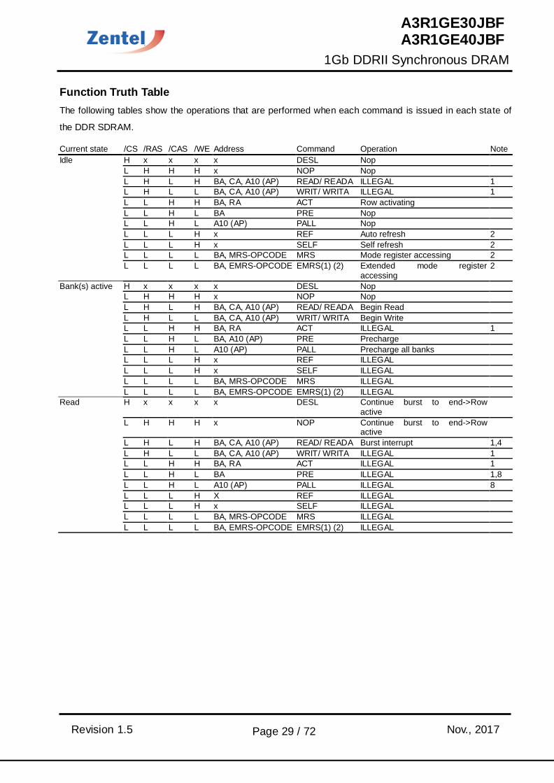
Burst Write Command [WRIT]
The Burst Write command is initiated by having /CS, /CAS and /WE low while holding /RAS high at the rising edge of the
clock. The address inputs determine the starting column address. Write latency (WL) is defined by a read latency (RL)
minus one and is equal to (AL + CL – 1) A data strobe signal (DQS) should be driven low (preamble) one clock prior to the
WL. The first data bit of the burst cycle must be applied to the DQ pins at the first rising edge o the DQS following the
preamble. The tDQSS specification must be satisfied for write cycles. The subsequent burst bit data are issued on
successive edge of the DQS until the burst length of 4 is completed. When the burst has finished, any additional data
supplied to the DQ pins will be ignored. The DQ Signal is ignored after the burst write operation is complete. The time
from the completion of the burst write to bank precharge is the write recovery time (tWR).

A3R1GE30JBF A3R1GE40JBF
1Gb DDRII Synchronous DRAM
Revision 1.5 Nov., 2017
Page 51 / 72
The minimum number of clock from the burst write command to the burst read command is CL - 1 + BL/2 + a write
to-read- turn-around-time (tWTR). This tWTR is not a write recovery time (tWR) but the time required to transfer the 4bit
write data from the input buffer into sense amplifiers in the array.
Enabling a write command every other clock supports the seamless burst write operation. This operation is allowed
regardless of same or different banks as long as the banks are activated.

A3R1GE30JBF A3R1GE40JBF
1Gb DDRII Synchronous DRAM
Revision 1.5 Nov., 2017
Page 52 / 72
Notes:1.Write burst interrupt function is only allowed on burst of 8. Burst interrupt o 4 is prohibited.
2.Write burst of 8 can only be interrupted by another write command. Write burst interruption by read command or
precharge command is prohibited.
3.Write burst interrupt must occur exactly two clocks after previous write command. Any other write burst interrupt
timings are prohibited.
4.Write burst interruption is allowed to any bank inside DRAM.
5.Write burst with auto precharge enabled is not allowed to interrupt.
6.Write burst interruption is allowed by another write with auto precharge command.
7.All command timings are referenced to burst length set in the mode register. They are not referenced to actual
burst. For example, minimum write to precharge timing is WL+BL/2+tWR where tWR starts with the rising clock
after the un-interrupted burst end and not from the end of actual burst end.

A3R1GE30JBF A3R1GE40JBF
1Gb DDRII Synchronous DRAM
Revision 1.5 Nov., 2017
Page 53 / 72
Write Data Mask
One write data mask (DM) pin for each 8 data bits (DQ) will be supported on DDR2 SDRAMs, Consistent with the
implementation on DDR2 SDRAMs. It has identical timings on write operations as the data bits, and though used in a
unidirectional manner, is internally loaded identically to data bits to insure matched system timing. DM is not used during
read cycles.

A3R1GE30JBF A3R1GE40JBF
1Gb DDRII Synchronous DRAM
Revision 1.5 Nov., 2017
Page 54 / 72
Precharge command [PRE]
The precharge command is used to precharge or close a bank that has been activated. The precharge command is
triggered when /CS, /RAS and /WE are low and /CAS is high at the rising edge of the clock. The precharge command can
be used to precharge each bank independently or all banks simultaneously. Three address bits A10, BA0, BA1 and BA2
are used to define which bank to precharge when the command is issued.
[Bank Selection for Precharge by Address Bits]
A10 BA0 BA1 BA2 Precharged Bank(s)
L L L L Bank 0 only
L H L L Bank 1 only
L L H L Bank 2 only
L H H L Bank 3 only
L L L H Bank 4 only
L H L H Bank 5 only
L L H H Bank 6 only
L H H H Bank 7 only
H x x x All banks 0 to 7
Remark: H: VIH, L:VIL, x: VIH or VIL
Burst Read Operation Followed by Precharge
Minimum read to precharge command spacing to the same bank = AL + BL/2 + max(RTP, 2) -2 clocks
For the earliest possible precharge, the precharge command may be issued on the rising edge that is “Additive latency
(AL) + BL/2 + max(RTP, 2) -2 clocks” after a Read command. A new bank active (command) may be issued to the same
bank after the RAS precharge time (tRP). A precharge command cannot be issued until tRAS is satisfied.

A3R1GE30JBF A3R1GE40JBF
1Gb DDRII Synchronous DRAM
Revision 1.5 Nov., 2017
Page 55 / 72

A3R1GE30JBF A3R1GE40JBF
1Gb DDRII Synchronous DRAM
Revision 1.5 Nov., 2017
Page 56 / 72
Burst Write followed by Precharge
Minimum Write to Precharge Command spacing to the same bank = WL + B/2 clocks + tWR
For write cycles, a delay must be satisfied from the completion of the last burst write cycle until the precharge command
can be issued. This delay is known as a write recovery time (tWR) referenced from the completion of the burst write to the
precharge command. No precharge command should be issued prior to the tWR delay, as DDR2 SDRAM allows the burst
interrupt operation only Read by Read or Write by Write at the boundary of burst 4.

A3R1GE30JBF A3R1GE40JBF
1Gb DDRII Synchronous DRAM
Revision 1.5 Nov., 2017
Page 57 / 72

A3R1GE30JBF A3R1GE40JBF
1Gb DDRII Synchronous DRAM
Revision 1.5 Nov., 2017
Page 58 / 72
Auto-Precharge Operation
Before a new row in an active bank can be opened, the active bank must be precharged using either the precharge
command or the auto-precharge function. When a read or a write command is given to the DDR2 SDRAM, the /CAS
timing accepts one extra address, column address A10, to allow the active bank to automatically begin precharge at the
earliest possible moment during the burst read or write cycle. If A10 is low when the read or write Command is issued,
then normal read or write burst operation is executed and the bank remains active at the completion of the burst
sequence. If A10 is high when the Read or Write Command is issued, then the auto-precharge function is engaged.
During auto-precharge, a read Command will execute as normal with the exception that the active bank will begin to
precharge on the rising edge which is /CAS latency (CL) clock cycles before the end of the read burst.
Auto-precharge can also be implemented during Write commands. The precharge operation engaged by the Auto
precharge command will not begin until the last data of the burst write sequence is properly stored in the memory array.
This feature allows the precharge operation to be partially or completely hidden during burst read cycles (dependent upon
/CAS latency) thus improving system performance for random data access. The /RAS lockout circuit internally delays the
Precharge operation until the array restore operation has been completed so that the auto precharge command may be
issued with any read or write command
Burst Read with Auto Precharge [READA]
If A10 is high when a Read Command is issued, the Read with Auto-Precharge function is engaged. The DDR2 SDRAM
starts an auto precharge operation on the rising edge which is (AL + BL/2) cycles later from the read with AP command
when the condition that. When tRAS(min) is satisfied. If tRAS (min.) is not satisfied at the edge, the start point of
auto-precharge operation will be delayed until tRAS (min.) is satisfied. A new bank active (command) may be issued to
the same bank if the following two conditions are satisfied simultaneously.
(1)The /RAS precharge time (tRP) has been satisfied from the clock at which the auto precharge begins.
(2)The /RAS cycle time (tRC) from the previous bank activation has been satisfied.

A3R1GE30JBF A3R1GE40JBF
1Gb DDRII Synchronous DRAM
Revision 1.5 Nov., 2017
Page 59 / 72

A3R1GE30JBF A3R1GE40JBF
1Gb DDRII Synchronous DRAM
Revision 1.5 Nov., 2017
Page 60 / 72
Burst Write with Auto-Precharge [WRITA]
If A10 is high when a write command is issued, the Write with auto-precharge function is engaged. The DDR2 SDRAM
automatically begins precharge operation after the completion of the burst writes plus write recovery time (tWR). The bank
undergoing auto-prcharge from the completion of the write burst may be reactivated if the following two conditions are
satisfied.
(1)The data-in to bank activate delay time (tWR + tRP) has been satisfied.
(2)The /RAS cycle time (tRC) from the previous bank activation has been satisfied.

A3R1GE30JBF A3R1GE40JBF
1Gb DDRII Synchronous DRAM
Revision 1.5 Nov., 2017
Page 61 / 72

A3R1GE30JBF A3R1GE40JBF
1Gb DDRII Synchronous DRAM
Revision 1.5 Nov., 2017
Page 62 / 72
Refresh Requirements
DDR2 SDRAM requires a refresh of all rows in any rolling 64ms interval. Each refresh is generated in one of two ways: by
an explicit automatic refresh command, or by an internally timed event in self-refresh mode. Dividing the number of device
rows into the rolling 64 ms interval defines the average refresh interval, tREFI, which is a guideline to controllers for
distributed refresh timing.
Automatic Refresh Command [REF]
When /CS, /RAS and /CAS are held low and /WE high at the rising edge of the clock, the chip enters the automatic
refresh mode (REF). All banks of the DDR2 SDRAM must be precharged and idle for a minimum of the precharge time
(tRP) before the auto refresh command (REF) can be applied. An address counter, internal to the device supplies the
bank address during the refresh cycle. No control of the external address bus is required once this cycle has started.
When the refresh cycle has completed, all banks of the DDR2 SDRAM will be in the precharged (idle) state. A delay
between the auto refresh command (REF) and the next activate command or subsequent auto refresh command must be
greater than or equal to the auto refresh cycle time (tRFC).
To allow for improved efficiency in scheduling and switching between tasks, some flexibility in the absolute refresh interval
is provided. A maximum of 8 refresh commands can be posted to any given DDR2 SDRAM, meaning that the maximum
absolute interval between any refresh command and the next Refresh command is 9 x tREFI.

A3R1GE30JBF A3R1GE40JBF
1Gb DDRII Synchronous DRAM
Revision 1.5 Nov., 2017
Page 63 / 72
Self Refresh Command [SELF]
The DDR2 SDRAM device has a built-in timer to accommodate self-refresh operation. The self-refresh command is
defined by having /CS, /RAS, /CAS and CKE held low with /WE high at the rising edge of the clock.
ODT must be turned off before issuing self refresh command by either driving ODT pin low or using EMRS command.
Once the command is registered, CKE must be held low to keep the device in self-refresh mode.
When the DDR2 SDRAM has entered self refresh mode all of the external signals except CKE, are “don’t care”. The clock
is internally disabled during self-refresh operation to save power. The user may change the external clock frequency or
halt the external clock one clock after Self-Refresh entry is registered, however, the clock must be restarted and stable
before the device can exit self refresh operation. Once self-refresh exit command is registered, a delay equal or longer
than the tXSNR or tXSRD must be satisfied before a valid command can be issued to the device. CKE must remain high
for the entire self-refresh exit period tXSRD for proper operation except for self refresh re-entry. Upon exit from self
refresh, the DDR2 SDRAM can be put back into self refresh mode after waiting at least tXSNR period and issuing one
refresh command (refresh period of tRFC). NOP or deselect commands must be registered on each positive clock edge
during the self-refresh exit interval. ODT should also be turned off during tXSRD.

A3R1GE30JBF A3R1GE40JBF
1Gb DDRII Synchronous DRAM
Revision 1.5 Nov., 2017
Page 64 / 72
Power-Down [PDEN]
Power-down is synchronously entered when CKE is registered low (along with NOP or deselect command). CKE is not
allowed to go low while mode register or extended mode register command time, or read or write operation is in progress.
CKE is allowed to go low while any of other operations such as row activation, precharge or auto-precharge, or
auto-refresh is in progress, but power-down IDD spec will not be applied until finishing those operations. Timing diagrams
are shown in the following pages with details for entry into power down.
The DLL should be in a locked state when power-down is entered. Otherwise DLL should be reset after exiting
power-down mod for proper read operation
If power-down occurs when all banks are idle, this mode is referred to as precharge power-down; If power down occurs
when there is a row active in any bank, this mode is referred to as active power-down. Entering power-down deactivates
the input and output buffers, excluding CK, /CK, ODT and CKE. Also the DLL is disable upon entering precharge
power-down or slow exit active power-down, but the DLL is kept enabled during fast exit active power-down. In
power-down mode, CKE low and a stable clock signal must be maintained at the inputs of the DDR2 SDRAM, and ODT
should be in a valid state but all other input signals are “Don’t Care”. CKE low must be maintained until tCKE has been
satisfied. Maximum power-down duration is limited by 9 times tREFI of the device.
The power-down state is synchronously exited when CKE is registered high (along with a NOP or deselect command).
CKE high must be maintained until tCKE has been satisfied. A valid, executable command can be applied with
power-down exit latency, tXP, tXARD, or tXARDS, after CKE goes high. Power-down exit latency is defined at AC
Characteristics table of this data sheet.

A3R1GE30JBF A3R1GE40JBF
1Gb DDRII Synchronous DRAM
Revision 1.5 Nov., 2017
Page 65 / 72
Read with Auto Precharge to Power-Down Entry
Write to Power-Down Entry

A3R1GE30JBF A3R1GE40JBF
1Gb DDRII Synchronous DRAM
Revision 1.5 Nov., 2017
Page 66 / 72
Write with Auto Precharge to Power-Down Entry

A3R1GE30JBF A3R1GE40JBF
1Gb DDRII Synchronous DRAM
Revision 1.5 Nov., 2017
Page 67 / 72

A3R1GE30JBF A3R1GE40JBF
1Gb DDRII Synchronous DRAM
Revision 1.5 Nov., 2017
Page 68 / 72
Asynchronous CKE Low Event
DRAM requires CKE to be maintained high for all valid operations as defined in this data sheet. If CKE asynchronously
drops low during any valid operation DRAM is not guaranteed to preserve the contents of array. If this event occurs,
memory controller must satisfy DRAM timing specification tDELAY before turning off the clocks.
Stable clocks must exist at the input of DRAM before CKE is raised high again. DRAM must be fully re-initialized (steps 4
through 13) as described in initialization sequence. DRAM is ready for normal operation after the initialization sequence.
See AC Characteristics table for tDELAY specification.
SSC (Spread Spectrum Clocking)
Terms and definitions
fCK,min : Minimum frequency supported by the DRAM (1/tCK(avg),max = 125MHz)
fCK,max : Maximum frequency supported by the DRAM (1/tCK(avg),min = 533MHz(-AH), 400MHz(-8E))
SSC band : If the system modulates the input clock frequency between fSSC,min and fSSC,max , this frequency band is
referred to as SSC band.
fSSC,nom : Mean frequency of fSSC,min and fSSC,max
Modulation frequency : Rate at which the frequency is modulated for SSC
Ex) 20kHZ modulation : Input clock frequency shifts gradually from fSSC,min to fSSC,max over 25us (50us/2).
SSC (Spread Spectrum Clocking) Criteria
SSC is allowed only if fSSC,min is greater than or equal to fCK,min and fSSC,max is less than or equal to fCK,max. All
input clock specs including, but not limited to, tERR(nper) must be met at all times. Allowed modulation frequency is
20kHz to 60kHz.
Allowed SSC band
If the DRAM DLL is locked at fSSC,nom (by issuing a DLL reset and waiting 200 clock cycles) and then the SSC is turned
on later, the system is allowed an SSC band of fSSC,nom +/- 1%.
In all other cases, the system is allowed an SSC band of fSSC,nom +/- 0.5%.
If the input clock frequency drifts out of this band, the output timings can no longer be guaranteed and DLL reset must be
issued to regain the output timings assuming a different SSC band.

A3R1GE30JBF A3R1GE40JBF
1Gb DDRII Synchronous DRAM
Revision 1.5 Nov., 2017
Page 69 / 72
Input Clock Frequency Change during Precharge Power Down
DDR2 SDARM input clock frequency can be changed under following condition:
DDR2 SDRAM is in precharged power down mode. ODT must be turned off and CKE must be at logic low level.
A minimum of 2 clocks must be waited after CKE goes low before clock frequency may change. SDRAM input clock
frequency is allowed to change only within minimum and maximum operating frequency specified for the particular speed
grade. During input clock frequency change, ODT and CKE must be held at stable low levels.
Once input clock frequency is changed, stable new clocks must be provided to DRAM before precharge power down may
be exited and DLL must be RESET via MRS after precharge power down exit. Depending on new clock frequency an
additional MRS or EMRS command may need to be issued to appropriately set the WR, CL and so on. During DLL relock
period, ODT must remain off. After the DLL lock time, the DRAM is ready to operate with new clock frequency.
Clock Frequency Change in Precharge Power Down Mode
No Operation command [NOP]
The no operation command should be used in cases when the DDR2 SDRAM is in an idle or a wait state The purpose of
the no operation command is to prevent the DDR2 SDRAM from registering any unwanted commands between
operations. A no operation command is registered when /CS is low with /RAS, /CAS, and /WE held high at the rising edge
of the clock. A no operation command will not terminate a previous operation that is still executing, such as a burst read or
write cycle.
Deselect Command [DESL]
The deselect command performs the same function as a no operation command. Deselect command occurs when /CS is
brought high at the rising edge of the clock, the /RAS, /CAS, and /WE signals become don’t cares.

A3R1GE30JBF A3R1GE40JBF
1Gb DDRII Synchronous DRAM
Revision 1.5 Nov., 2017
Page 70 / 72
Package Drawing
60-ball FBGA
Solder ball: Lead free (Sn-Ag-Cu) Unit: mm

A3R1GE30JBF A3R1GE40JBF
1Gb DDRII Synchronous DRAM
Revision 1.5 Nov., 2017
Page 71 / 72
84-ball FBGA
Solder ball: Lead free (Sn-Ag-Cu) Unit: mm

A3R1GE30JBF A3R1GE40JBF
1Gb DDRII Synchronous DRAM
Revision 1.5 Nov., 2017
Page 72 / 72
Recommended Soldering Conditions
Please consult with our sales offices for soldering conditions of the A3R1GE30JBF, A3R1GE40JBF.
Type of Surface Mount Device
A3R1GE30JBF: 60-ball FBGA<Lead free(Sn-Ag-Cu)>
A3R1GE40JBF: 84-ball FBGA<Lead free(Sn-Ag-Cu)>
Zentel DRAM products are not intended for medical implementation, airplane and transportation
instrument, safety equipments, or any other applications for life support or where Zentel products
failure could result in life loss, personal injury, or environment damage. Zentel customers who
purchase Zentel products for use in such applications do so in their own risk and fully agree Zentel
accepts no liability for any damage from this improper use.
Important Notice:
Related Documents