Retrospective eses and Dissertations Iowa State University Capstones, eses and Dissertations 1997 500mV low-voltage operational amplifier design Jian Zhou Iowa State University Follow this and additional works at: hps://lib.dr.iastate.edu/rtd Part of the Power and Energy Commons , and the VLSI and Circuits, Embedded and Hardware Systems Commons is esis is brought to you for free and open access by the Iowa State University Capstones, eses and Dissertations at Iowa State University Digital Repository. It has been accepted for inclusion in Retrospective eses and Dissertations by an authorized administrator of Iowa State University Digital Repository. For more information, please contact [email protected]. Recommended Citation Zhou, Jian, "500mV low-voltage operational amplifier design" (1997). Retrospective eses and Dissertations. 16751. hps://lib.dr.iastate.edu/rtd/16751

Welcome message from author
This document is posted to help you gain knowledge. Please leave a comment to let me know what you think about it! Share it to your friends and learn new things together.
Transcript
Retrospective Theses and Dissertations Iowa State University Capstones, Theses andDissertations
1997
500mV low-voltage operational amplifier designJian ZhouIowa State University
Follow this and additional works at: https://lib.dr.iastate.edu/rtd
Part of the Power and Energy Commons, and the VLSI and Circuits, Embedded and HardwareSystems Commons
This Thesis is brought to you for free and open access by the Iowa State University Capstones, Theses and Dissertations at Iowa State University DigitalRepository. It has been accepted for inclusion in Retrospective Theses and Dissertations by an authorized administrator of Iowa State University DigitalRepository. For more information, please contact [email protected].
Recommended CitationZhou, Jian, "500mV low-voltage operational amplifier design" (1997). Retrospective Theses and Dissertations. 16751.https://lib.dr.iastate.edu/rtd/16751
~.<,,"" / ' J.- ./#/(
/7 91 2-5 S/ '7-'
1..;. /
500m V low-voltage operational amplifier design
by
Jian Zhou
A thesis submitted to the graduate faculty
in partial fulfillment of the requirements for the degree of
MASTER OF SCIENCE
Major: Electrical Engineering
Major Professor: Randall Geiger
Iowa State University
Ames, Iowa
1997
Copyright © Jian Zhou, 1997. All rights reserved
ii
Graduate College
Iowa State University
This is to certify that the Master's thesis of
Jian Zhou
has met the thesis requirement of Iowa State University
Signatures have been redacted for privacy
III
TABLE OF CONTENTS
ACKNOWLEDGEMENTS
ABSTRACT
CHAPTER 1. INTRODUCTION
ix
x
1.1 Low voltage circuit design 1
1.2 Organization of the thesis 5
CHAPTER 2. MOSFET AND TWO STAGE OPERATIONAL AMPLIFIER DESIGN 7
2.1 Basic MOSFET operation 7
2.2 Small-signal model for MOSFETs 11
2.3 MOS transistor as a transmission gate 14
2.4 Two-stage operational amplifier design 15
CHAPTER 3. LOW-VOLTAGE OPERATIONAL AMPLIFIER DESIGN 19
3.1 Previous work 19
3.2 Threshold voltage tuning 21
3.3 Threshold tunable low-voltage operational amplifier 22
3.4 500m V operational amplifier design 23
3.5 DC voltage source 27
3.6 Simulation results 30
3.7 Conclusion 37
CHAPTER 4. SUPPLEMENTARY CIRCUIT IMPLEMENTATIONS 39
4.1 Supplementary circuits 39
4.2 Reference voltage generation 40
4.3 High voltage and negative voltage generator 47
IV
4.4 Oscillator 50
4.5 Nonoverlapping clocks 54
4.6 Pulse generator 56
4.7 Conclusion 56
CHAPTER 5: CONCLUSIONS 58
APPENDIX A: LEVEL 3 HSPICE MODEL 60
APPENDIX B: LEVEL 13 HSPICE MODEL 61
APPENDIX C: NETLIST FOR THE CIRCUIT SIMULATION 63
BIBIOGRAPHY 73
v
LIST OF FIGURES
Figure 1.1 Supply voltage scaling 2
Figure 1.2 Power supply and power dissipation in previous work 5
Figure 2.1 (a) Structure of an nMOSFET and a pMOSFET (b) Top view of the nMOSFET and pMOSFET 8
Figure 2.2 MOSFET operational structure 9
Figure 2.3 Output characteristic of the nMOSFET 11
Figure 2.4 Small-signal model of the MOSFET 12
Figure 2.5 Simplified small-signal model for the MOSFET 13
Figure 2.6· (a)nMOS transistor as a transmission gate (b)Transfer characteristics of an nMOS pass transistor 14
Figure 2.7 (a)pMOS transistor as a transmission gate (b)Transfer characteristics of a pMOS pass transistor 15
Figure 2.8 Schematic of a two-stage operational amplifier 16
Figure 3.1 Complementary differential input stage 19
Figure 3.2 Floating gate MOS transistor cell 19
Figure 3.3 Threshold voltage tunable structure 21
Figure 3.4 Threshold voltage tuning effects 22
Figure 3.5 Threshold tunable low-voltage operational amplifier 22
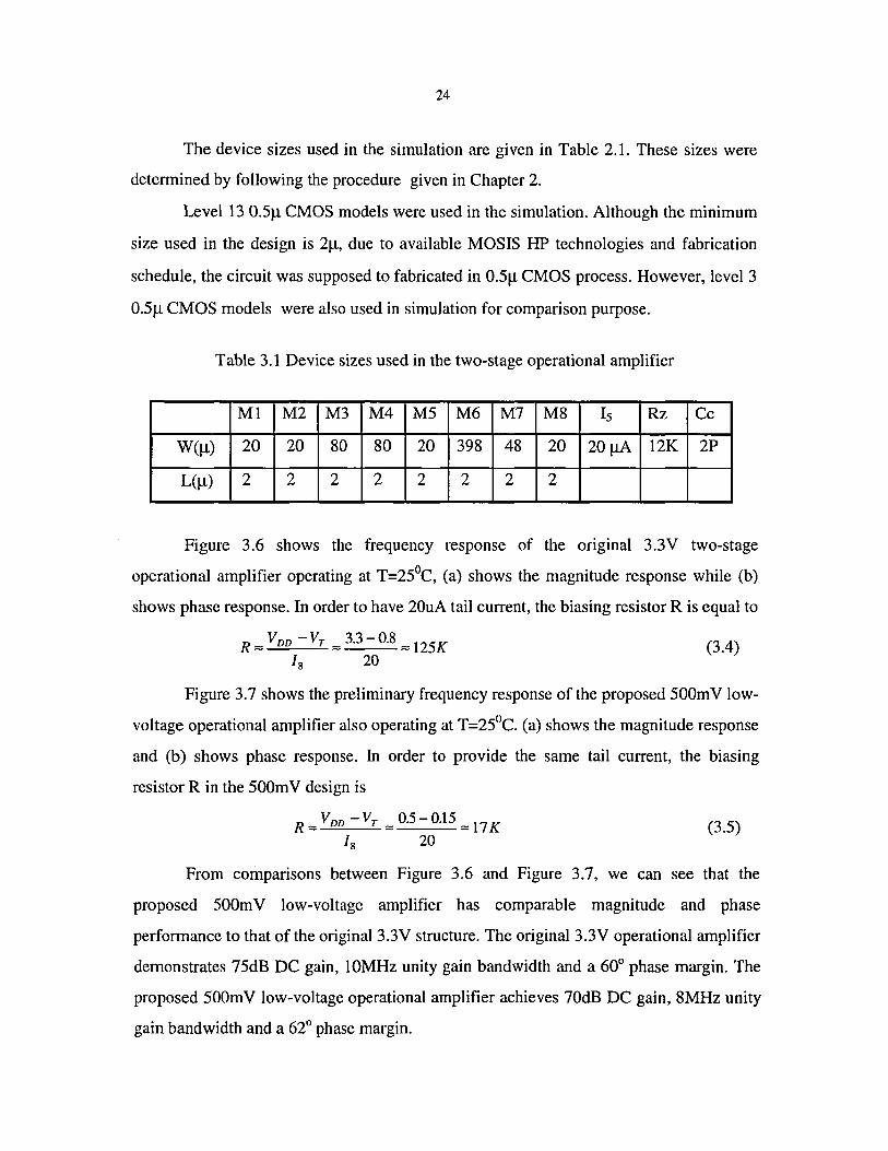
Figure 3.6 Frequency response of the original two-stage operational amplifier (a) Magnitude response (b) Phase response 25
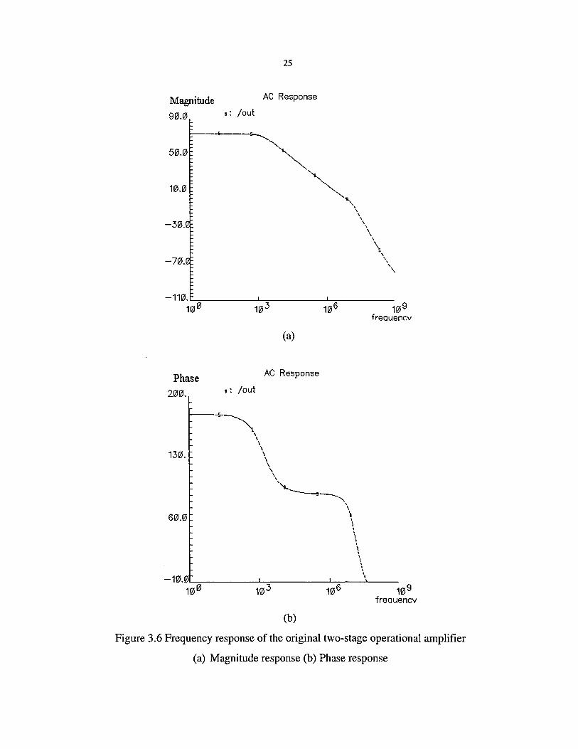
Figure 3.7 Frequency response of the proposed 500mV low voltage operational amplifier. (a) Magnitude response (b) Phase response 26
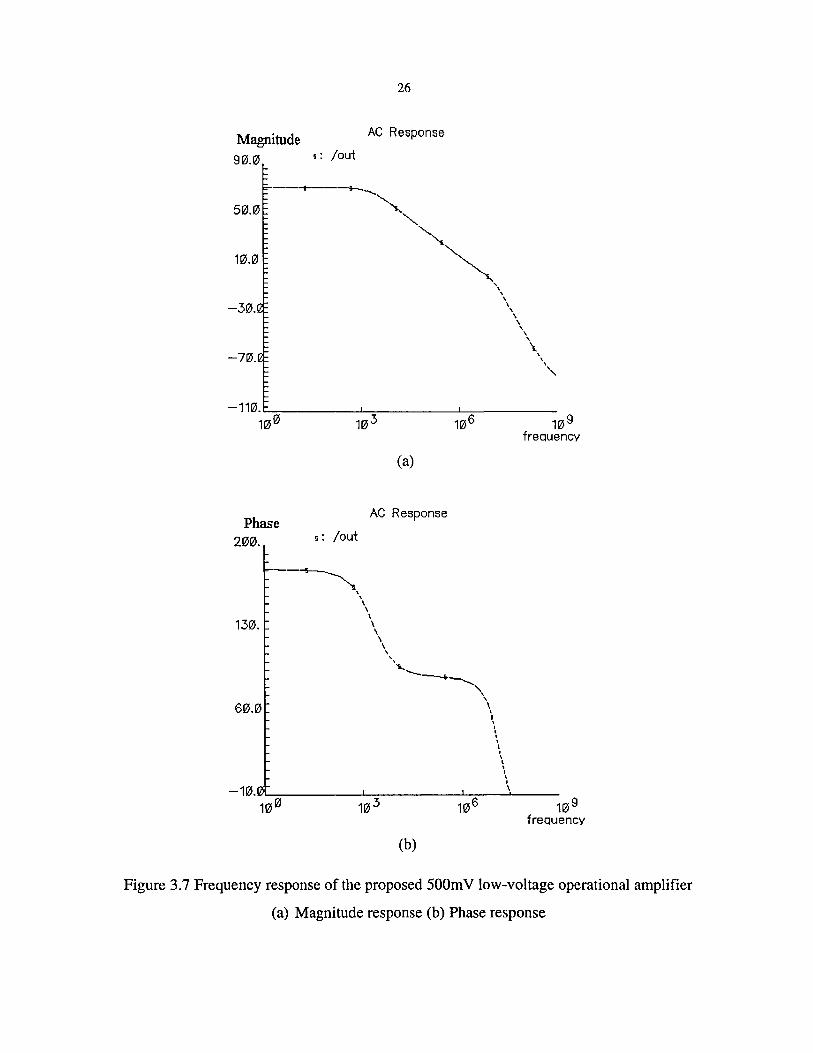
Figure 3.8 DC voltage source (a) Symbol (b) Circuit implementation 27
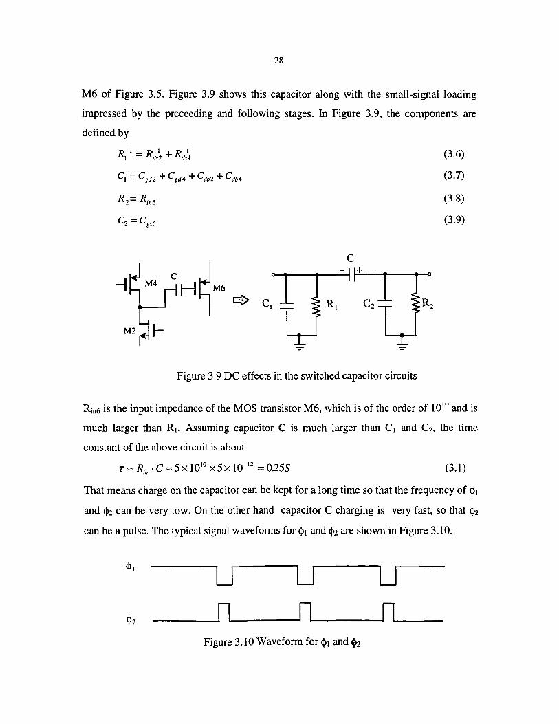
Figure 3.9 DC effects in the switched capacitor circuits 28
Figure 3.10 Waveform for <1>1 and <1>2 28
vi
Figure 3.11 Small-signal model considering the capacitor effects 29
Figure 3.12 Leakage current effects and discharge circuit 30
Figure 3.13 Simulation circuit for the switched capacitor 31
Figure 3.14 Frequency response of the 500mV low voltage operational amplifier (a) Magnitude response (b) Phase response 32
Figure 3.15 (a) Test circuit for unity gain DC transfer characteristics (b) Test circuit for unity gain step response 34
Figure 3.16 (a) Unity gain DC transfer characteristics of the 3.3V operational amplifier (b) Unity gain DC transfer characteristic of the 500mV operational amplifier 35
Figure 3.17 (a) Unity gain step response of the 3.3V operational amplifier (b) Unity gain step response of the 500mV operational amplifier 36
Figure 3.18 Layout of the 500m V low-voltage operational amplifier core 38
Figure 4.1 Low-voltage operational amplifier architecture 39
Figure 4.2 Threshold voltage variation effects 40
Figure 4.3 Threshold voltage extraction 41
Figure 4.4 Block diagram and circuit of an attenuator consisting of two nMOSFETs 42
Figure 4.5 DC transfer characteristic of the attenuator consisting of two nMOSFETs 43
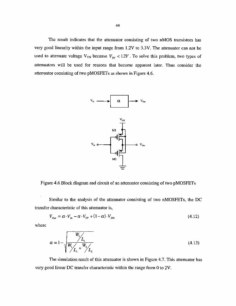
Figure 4.6 Block diagram and circuit of an attenuator consisting of two pMOSFETs 44
Figure 4.7 DC transfer characteristic of the attenuator consisting of two pMOSFETs 45
Figure 4.8 DC reference voltage generator for Approach I 46
Figure 4.9 DC reference voltage generator for Approach 2 47
Figure 4.10 (a)Charge pump circuit (b)Clock waveforms 48
Figure 4.11 Simulation results for the charge pump 49
Figure 4.12 Negative substrate voltage generator 49
Figure 4.13 Simulation result for the negative voltage generator 50
Figure 4.14 Ring oscillator 51
Vll
Figure 4.15 Cross section and top view of the floating gate transistor 52
Figure 4.16 A simplified capacitive equivalent circuit of the floating transistor 53
Figure 4.17 Circuit configuration of the bootstrapped buffer 54
Figure 4.18 Simulation results of the bootstrapped buffer 55
Figure 4.19 Nonoverlapping clock (a) Clock signals (b) Circuit implementation 55
Figure 4.20 Shift register as a pulse generator 56
VIII
LIST OF TABLES
Table 1.1 Low-voltage operational amplifier characteristics and techniques been used 4
Table 3.1 Device sizes used in the two-stage operational amplifier 22
Table 3.2 Simulated frequency response of the 500m V low-voltage operational amplifier 31
Table 3.3 Comparisons of performance parameters of the two operational amplifiers 34
Table 4.1 Power dissipation in the low-voltage operational amplifier circuits 54

IX
ACKNOWLEDGEMENTS
I would like to express my he artful appreciation to my major professor Dr.
Randall L. Geiger. I wish to thank him for his guidance, support and help throughout my
master program at Iowa State University. He introduced me to the challenging and
exciting Mixed-Signal and Analog VLSI field throughout his great course and research
guidance. He is always there ready for help whenever I have questions. His academic
excellence and foresight have been of great help to me and have had an important effect
on my life.
I would also like to express my thanks to my co-major professor Dr. Marwan
Hassoun. He br.ought me to Iowa State University and gave me a lot of encouragement. I
would like to express my appreciation to Dr. E. K. F. Lee for his constructive comments
and suggestions on the circuit implementation. I wish to acknowledge Dr. William Black
for his great course and instructions on the layout for the research project. I would also
like to thank Dr. David Kao for his time serving as my committee member.
Throughout my masters program, my colleagues gave me a lot of help, which
made my life enjoyable and productive. I would like to thank Huawen Jin for his
suggestions during various discussions which were of great help to my work. I would also
like to thank Xiaohong Du, Lin Wu and Yiqing Chen for being my course partners; we
really shared a lot of things together.
Lastly, I would like to thank my wife, parents and sisters for their endless love and
support in every respect.
x
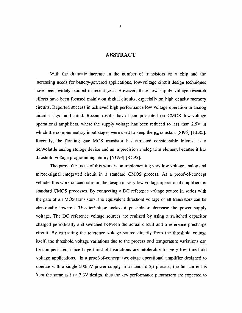
ABSTRACT
With the dramatic increase in the number of transistors on a chip and the
increasing needs for battery-powered applications, low-voltage circuit design techniques
have been widely studied in recent year. However, these low supply voltage research
efforts have been focused mainly on digital circuits, especially on high density memory
circuits. Reported success in achieved high performance low voltage operation in analog
circuits lags far behind. Recent results have been presented on CMOS low-voltage
operational amplifiers, where the supply voltage has been reduced to less than 2.SV in
which the complementary input stages were used to keep the gm constant [SI9S] [HL8S].
Recently, the floating gate MOS transistor has attracted considerable interest as a
nonvolatile analog storage device and as a precision analog trim element because it has
threshold voltage programming ability [YU93] [Re9S].
The particular focus of this work is on implementing very low voltage analog and
mixed-signal integrated circuit in a standard CMOS process. As a proof-of-concept
vehicle, this work concentrates on the design of very low voltage operational amplifiers in
standard CMOS processes. By connecting a DC reference voltage source in series with
the gate of all MOS transistors, the equivalent threshold voltage of all transistors can be
electrically lowered. This technique makes it possible to decrease the power supply
voltage. The DC reference voltage sources are realized by using a switched capacitor
charged periodically and switched between the actual circuit and a reference precharge
circuit. By extracting the reference voltage source directly from the threshold voltage
itself, the threshold voltage variations due to the process and temperature variations can
be compensated, since large threshold variations are intolerable for very low threshold
voltage applications. In a proof-of-concept two-stage operational amplifier designed to
operate with a single SOOmV power supply in a standard 2Jl process, the tail current is
kept the same as in a 3.3V design, thus the key performance parameters are expected to
xi
be maintained at reasonable values. The dramatic decrease of the power supply possible
with this approach is paralleled with a corresponding reduction in the power dissipation.
Simulation results of this 500m V operational amplifier show a 70dB DC gain, 7.8MHz
unity gain bandwidth and a 65° phase margin. Power dissipation is reduced by more than
90% from that of the corresponding 3.3V design.
Although the specific implementation is focused on the implementation of an
operational amplifier with comparable performance parameters to those with larger
supply voltage, the dominant applications of this technique are for designing a variety of
analog and mixed-signal systems that operate at very low voltages and with low power
dissipation.
CHAPTER 1. INTRODUCTION
This chapter gives the motivation behind this thesis work. The questions of why
low-voltage circuit design is important and why low-voltage operational amplifiers are
needed are answered. The chapter is concluded with a summary of the organization of
this thesis.
1.1 Low-voltage circuit design
During the past two decades, low supply voltage and low-power circuit design
techniques have attracted more and more interests and have been widely studied. The
motivation behind low-voltage and low-power circuit design is primarily due to three
reasons.
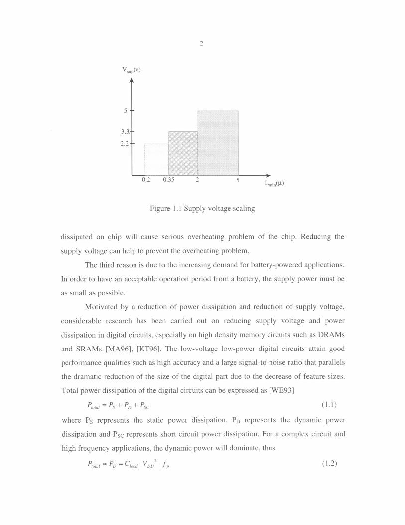
The first reason arises from constant reduction of the minimum feature size (i.e.
minimum gate length) of a MOS transistor. As the minimum channel length has been
scaled down to sub micron levels, the gate oxide thickness has been reduced to several
nanometers. With the decreasing thickness of gate oxide, the electric field strength in the
gate oxide for a fixed supply voltage increases sharply. To avoid gate breakdown and
ensure device reliability, the supply voltage has to be reduced. For the S micron to 2
micron range, SV supply voltage is widely used. Currently, 1.2 micron and O.S micron
processes use 3.3V to 2.SV supply voltages. It is expected that when minimum feature
sizes are scaled down to deep submicron levels, acceptable supply voltage will be 2.2V or
lower. This trend is illustrated in Figure 1.1.
The second reason emanates from the increasing density of components on chip.
With the increasing number of components integrated on a chip, more power will be
dissipated on chip if the same voltage and current levels are maintained. For example,
Pentium II has 7.S million transistors on chip and dissipates 43 Watts. Such high power
5
3
2.2
2
0.2 0.35 2 5
Figure 1.1 Supply voltage scaling
dissipated on chip will cause serious overheating problem of the chip. Reducing the
supply voltage can help to prevent the overheating problem.
The third reason is due to the increasing demand for battery-powered applications.
In order to have an acceptable operation period from a battery, the supply power must be
as small as possible.
Motivated by a reduction of power dissipation and reduction of supply voltage,
considerable research has been carried out on reducing supply voltage and power
dissipation in digital circuits, especially on high density memory circuits such as DRAMs
and SRAMs [MA96], [KT96]. The low-voltage low-power digital circuits attain good
performance qualities such as high accuracy and a large signal-to-noise ratio that parallels
the dramatic reduction of the size of the digital part due to the decrease of feature sizes.
Total power dissipation of the digital circuits can be expressed as [WE93]
(1.1 )
where Ps represents the static power dissipation, PD represents the dynamic power
dissipation and Psc represents short circuit power dissipation. For a complex circuit and
high frequency applications, the dynamic power will dominate, thus
(1.2)
3
where C)oad is the total load capacitance and fp is the operation frequency.
Equation (1.2) shows that the power dissipation is quadratically dependent on the
supply voltage VDD. Potential power reduction can be achieved by lowing the supply
voltage.
Paralleling the increasing role of digital circuits in current signal processing
systems are increasing perfonnance expectations being placed on analog circuits. This is
placing increasing demands on analog designers because the computer-aided analog
design tools have not reached the maturity of their digital counterparts. The necessity of
building these high perfonnance analog circuits becomes apparent by observing that
living in a real world, the signals to and from devices such as the sensors and actuators
which communicate with the outside world, are inherently analog. In order to keep pace
with the developments in digital circuit design, low-voltage low-power analog circuit
design become~ critical.
Low-voltage operation is being paralleled with the scaling of threshold voltages.
One of the most challenging difficulties imposed with the scaling of threshold voltages is
the increased relative threshold voltage variation. Threshold voltage scaling requires
complicated technology known as "substrate engineering" and the costs associated with
developing new and specialized processes that are sufficiently stable to support high
voltage commercial production are enonnous. A new method to electrically lower the
threshold voltage while still maintaining a standard process will be presented in this
work.
One of the most important analog building blocks is the operational amplifier. It
has found its way into numerous applications, such as switched capacitor filters, active
filters, charge amplifiers, data converters and more. The design of high performance low
voltage low-power operational amplifiers is one of the most challenging areas facing
analog circuit designers today. Many papers and books have been published on this
subject [HH96], [SI95].
A technique for dramatically reducing the power supply voltage for analog and
mixed-signal circuits will be introduced in this thesis. As a "proof of concept" for
4
employing this technique, a very-low-voltage operational amplifier will be designed.
Although the major emphasis in this is on the design of the operational amplifier, the
major contribution is in establishing that this basic approach to very-low-voltage design
is possible.
Low-voltage operational amplifier design can be divided into three groups, low
voltage, very-low-voltage and ultra-low-voltage. Operational amplifiers in the first group
can operate on supply voltages between 2V and 5V. At the lower end of this range, this
corresponds to about two stacked gate-source voltages and two stacked saturation
voltages. Operational amplifiers in the second group have supply voltages between 1 V
and 2V and typically provide the designer with only one gate-source voltage and one
saturation voltage. Operational amplifiers in the third group operate on supply voltages
below 1 V. There is little literature available in the ultra-low voltage range.
Most of previous work on low-voltage operational amplifier design belonged to
the previous two groups. Table 1.1 summarizes some previous work in the area and the
performance parameters they achieved.
Table 1.1: Low-voltage operational amplifier characteristics and techniques been used
VDD-VSS Gain Pdiss (W) Year Technique (dB)
Eggerrnont [EC96] 2 65 100Jl 1996 SOl CMOS & gmn+gmp
Huijsing [HL85] 1.5 100 0.3m 1985 BiCMOS & gmn+gmp
Fonderie [FM89] 1 100 10m 1989 BiCMOS & gmn+gmp
Huang [HC97] 1.5 100 0.89m 1997 BiCMOS & gmn+gmp
Sakurai [SI96] 2.5 80 -1m 1996 gmn+gmp
Allen [AB95] 1 >50 45Jl 1995 Bulk driven MOSFET
Angulo [AC95] 1.5 N/A N/A 1995 Floating gate
Figure 1.2 illustrates the power supply voltage and power dissipation achieved in
the previous work. We can see that the power supply voltage in all previous work was
higher than IV. No one has been successful at pushing the supply voltage down to lower
than IV. It can be further observed that progress in power supply voltage scaling has
slowed as designers approached the 1 V hurdle with 100m V decreases in power supply
Power
This work
•
I
•
•
5
• • Previous work
• • 2
Supply
Figure 1.2 Power supply and power dissipation in previous work
voltage being viewed as significant contributions. For the low supply voltage work
referenced, all approaches either utilized complementary input stages or utilized
specialized processes that are not widely available for commercial production.
This thesis presents a new method for designing ultra low-voltage operational
amplifiers. Some of the merits are list below:
• Utilizes existing standard process
• Ultra low supply voltage-O.5V
• Comparable key performance parameters to high-voltage designs
• Low power dissipation
1.2 Organization of the thesis
The main focus of this thesis will be to design a very low-voltage operational
amplifiers. Following this introduction, Chapter 2 will describe some general background
on MOSFETs and the design of operational amplifiers. Chapter 3 gives a literature review
on low-voltage operational amplifier design. This is followed by a discussion of the
proposed ultra low-voltage operational amplifier. In this chapter, design considerations
will be explained in detail. Chapter 4 provides the supplementary circuits that support the
6
ultra low-voltage operational amplifier. The threshold voltage variation compensation
technique is also described in more detail. Finally, Chapter 5 addresses conclusions and
future work on this topic.
7
CHAPTER 2. MOSFET AND TWO-STAGE OPERATIONAL
AMPLIFIER DESIGN
Before I start a discussion of the proposed operational amplifier structure, some
basic details regarding MOSFET operation will be given. The design procedure of a two
stage operational amplifier will follow.
2.1 Basic MOSFET operation
CMOS technology is widely used for designing integrated circuits over Bipolar
and MESFET technology due to the advantages such as greater density and simpler
process technology. CMOS technology provides two types of transistors, an n-type
transistor (nMOS) and a p-type transistor (pMOS) where electrons and holes provide the
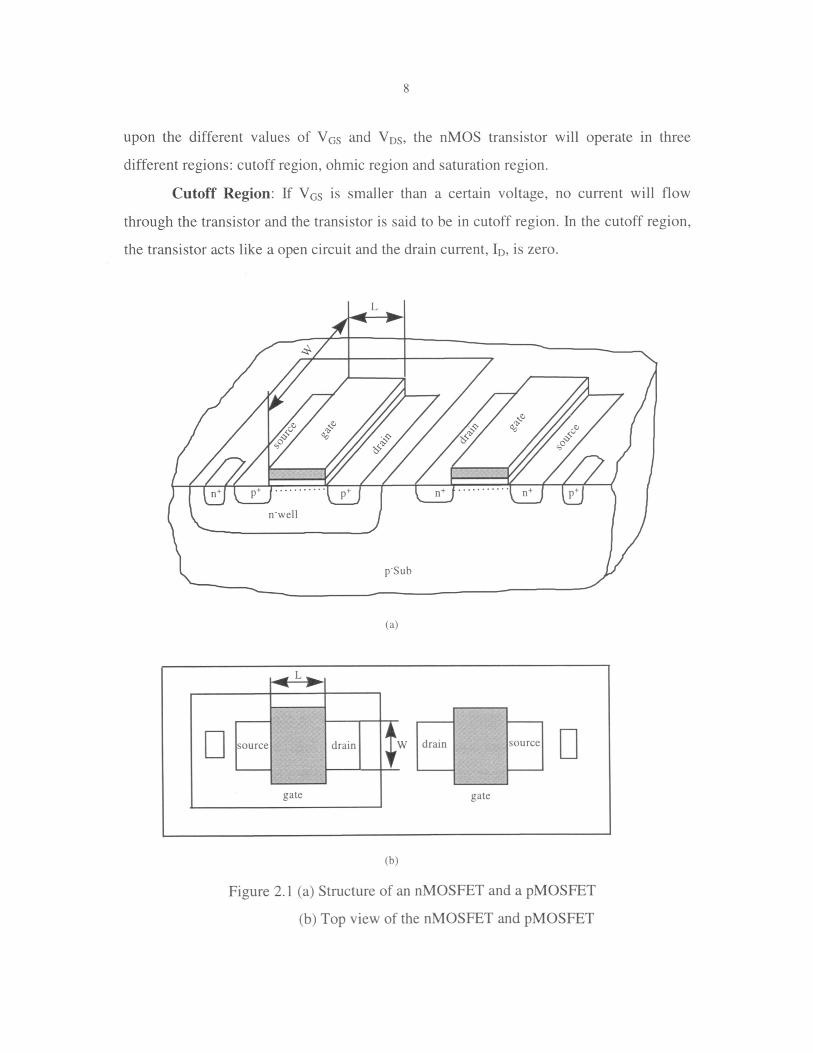
conduction mechanisms respectively. Figure 2.1 shows the typical physical structures for
the two types of MOS transistors. For the nMOS transistor, the lightly doped p- material
is called the substrate or bulk. The two heavily doped p+ regions diffused in the substrate
are called the drain and source regions respectively and are separated by a distance of L
(referred to as the device length). At the surface between the drain and the source lies a
gate electrode that is separated from the silicon by a thin dielectric material. Similarly, the
pMOS transistor is formed by two heavily doped p+ regions separating the lightly doped
n- well with a gate bridging the drain and the source.
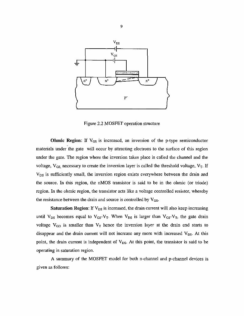
The MOSFET is fundamentally a voltage controlled current source with the
controlling voltage applied between the gate and the source. The basic operation of MOS
transistors will be for an nMOS transistor. The basic operation of a pMOS transistor is
the same. In Figure 2.2(a), we show an nMOS transistor where the source and the
substrate are grounded and the drain and the gate are tied to separate voltages. Based
8
upon the different values of VGS and VDS, the nMOS transistor will operate in three
different regions: cutoff region, ohmic region and saturation region.
Cutoff Region: If V GS is smaller than a certain voltage, no current will flow
through the transistor and the transistor is said to be in cutoff region. In the cutoff region,
the transistor acts like a open circuit and the drain current, ID, is zero.
D
L
(a)
,. L "", - ,.
- ~
A~ drain D Isource drain "w source
'--- -gate gate
(b)
Figure 2.1 (a) Structure of an nMOSFET and a pMOSFET
(b) Top view of the nMOSFET and pMOSFET
9
Figure 2.2 MOSFET operation structure
Ohmic Region: If V GS is increased, an inversion of the p-type semiconductor -
materials under the gate will occur by attracting electrons to the surface of this region
under the gate. The region where the inversion takes place is called the channel and the
voltage, V GS, necessary to create the inversion layer is called the threshold voltage, VT. If
Vos is sufficiently small, the inversion region exists everywhere between the drain and
the source. In this region, the nMOS transistor is said to be in the ohmic (or triode)
region. In the ohmic region, the transistor acts like a voltage controlled resistor, whereby
the resistance between the drain and source is controlled by V GS.
Saturation Region: If Vos is increased, the drain current will also keep increasing
until Vos becomes equal to VGS-VT• When Vos is larger than VGS-VT, the gate drain
voltage V GO is smaller than VT hence the inversion layer at the drain end starts to
disappear and the drain current will not increase any more with increased Vos. At this
point, the drain current is independent of Vos. At this point, the transistor is said to be
operating in saturation region.
A summary of the MOSFET model for both n-channel and p-channel devices is
given as follows:
10
nMOS transistor
o V GS < V T' V os ~ 0 (cutoff)
J1n.Cox .W(v -v - VDS).v (l+A..V ) L GS T 2 DS DS V GS > V T' 0 < V DS < V GS - V T (ohmic)
J1n' Cox' W (v _ V )2. (1 + A.. V ) 2. L GS T DS
(2.1)
where,
pMOS transistor
o V GS > VT, Vos ~ 0 (cutoff)
_/lP.Cox.W(v -v _ VDS).v (l-A..V ) L GS T 2 DS DS V GS < V T' 0 > V DS > V GS - V T ( ohmic)
_ /lP,Cox 'W(v _V)2 .(l-A..V ) 2. L GS T DS V GS < V T' Vos < V GS - V T(saturation)
where,
The various parameters used in above equation are defined as
Jln = surface mobility of the channel for the nMOS transistor
Jlp = surface mobility of the channel for the pMOS transistor
Cox = capacitance per unit area of the gate oxide
W = effective channel width
L = effective channel length
A = channel length modulation parameter
'Y = bulk threshold parameter
<I> = strong inversion surface potential
(2.2)
The output characteristics of the MOS transistor can be developed from the above
equations. Figure 2.3 shows these characteristics. The solid line in the figure corresponds
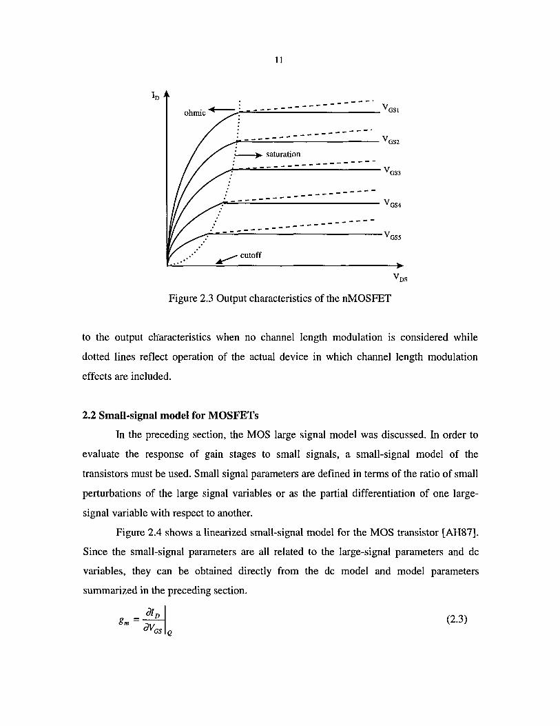
11
-- - -' +-: __ - - - - - - - - - - - V GSI ohmic -:;...-......... ::...::;.."'-----------
-- -' ----~ .... -:...:-::...;:;.-.;;..-_-_-_-_-_-_-_-_____ V GS2
.~ saturation
--------------~---=-=...;;;...-------- VGS3
---------------~o..:...;-::...;;;.---------------- V GS4
---------------------·---=--..:;.-..;;--------------V GS5
~cutoff
Figure 2.3 Output characteristics of the nMOSFET
to the output cliaracteristics when no channel length modulation is considered while
dotted lines reflect operation of the actual device in which channel length modulation
effects are included.
2.2 Small-signal model for MOSFETs
In the preceding section, the MOS large signal model was discussed. In order to
evaluate the response of gain stages to small signals, a small-signal model of the
transistors must be used. Small signal parameters are defined in terms of the ratio of small
perturbations of the large signal variables or as the partial differentiation of one large
signal variable with respect to another.
Figure 2.4 shows a linearized small-signal model for the MOS transistor [AH87].
Since the small-signal parameters are all related to the large-signal parameters and dc
variables, they can be obtained directly from the dc model and model parameters
summarized in the preceding section.
~IJD g = m avGS Q
(2.3)
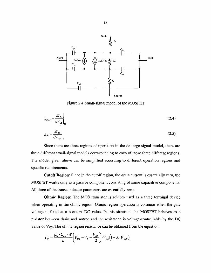
Gate
~IJD gmbs = av BS Q
g,,= JED I avDS Q
12
Bulk
Source
Figure 2.4 Small-signal model of the MOSFET
(2.4)
(2.5)
Since there are three regions of operation in the dc large-signal model, there are
three different small-signal models corresponding to each of these three different regions.
The model given above can be simplified according to different operation regions and
specific requirements.
Cutoff Region: Since in the cutoff region, the drain current is essentially zero, the
MOSFET works only as a passive component consisting of some capacitive components.
All three of the transconductor parameters are essentially zero.
Ohmic Region: The MOS transistor is seldom used as a three terminal device
when operating in the ohmic region. Ohmic region operation is common when the gate
voltage is fixed at a constant DC value. In this situation, the MOSFET behaves as a
resistor between drain and source and the resistance is voltage-controllable by the DC
value of V GS. The ohmic region resistance can be obtained from the equation
13
neglecting the /.. effect, we obtain the resistance
RFET =::S = /L. C" {:} (VGS - VT - VDS ) (2.6)
For the case V ds is very close to zero,
(2.7)
The MOSFET normally will not be biased in the ohmic region due to the performance
limitation.
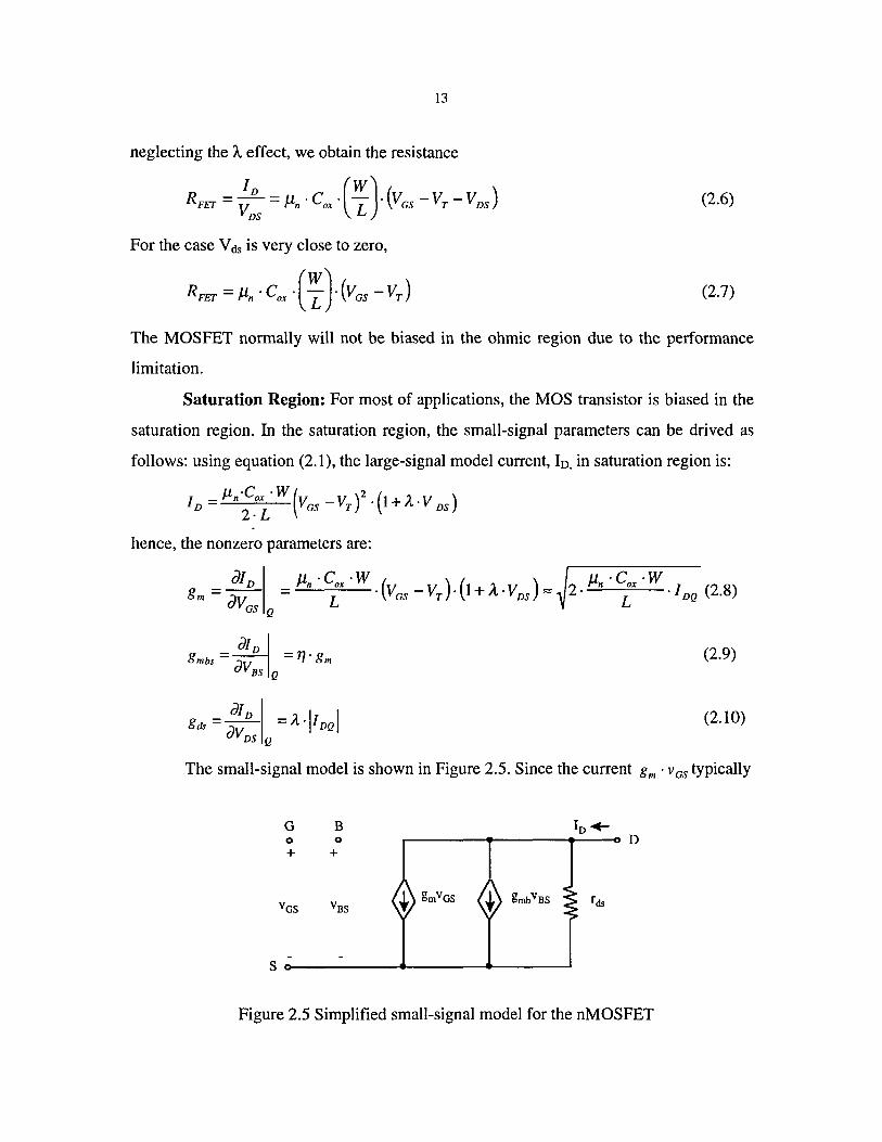
Saturation Region: For most of applications, the MOS transistor is biased in the
saturation region. In the saturation region, the small-signal parameters can be drived as
follows: using equation (2.1), the large-signal model current, ID, in saturation region is:
hence, the nonzero parameters are:
(2.9)
gds = dID =l·IIDQI avDS Q
(2.10)
The small-signal model is shown in Figure 2.5. Since the current gm . VGS typically
G o +
B o ~-------.------~~---o D
+
s ~--------~~------~------~
Figure 2.5 Simplified small-signal model for the nMOSFET
14
will dominate the drain current, the small-signal MOS transistor is inherently a good
transconductance amplifier [GA90].
2.3 MOS transistor as a transmission gate
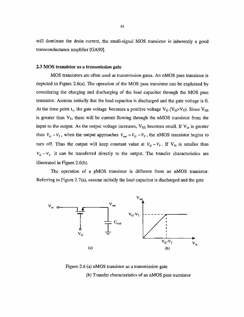
MOS transistors are often used as transmission gates. An nMOS pass transistor is
depicted in Figure 2.6(a). The operation of the MOS pass transistor can be explained by
considering the charging and discharging of the load capacitor through the MOS pass
transistor. Assume initially that the load capacitor is discharged and the gate voltage is O.
At the time point t}, the gate voltage becomes a positive voltage Vo (VO>VT). Since Vos
is greater than VT, there will be current flowing through the nMOS transistor from the
input to the output. As the output voltage increases, Vos becomes small. If Yin is greater
than VG - Vr , when the output approaches Vaut = V G - Vr , the nMOS transistor begins to
tum off. Thus the output will keep constant value at VG - Vr . If Yin is smaller than
VG - Vr it can be transferred directly to the output. The transfer characteristics are
illustrated in Figure 2.6(b).
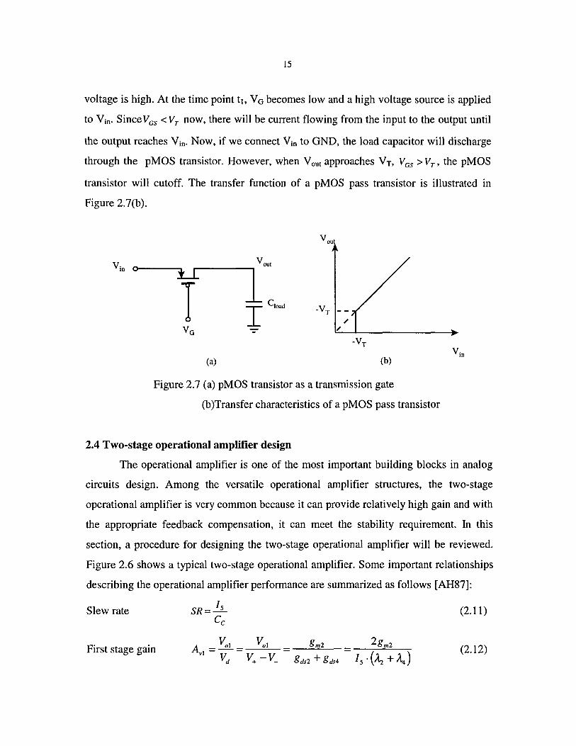
The operation of a pMOS transistor is different from an nMOS transistor.
Referring to Figure 2.7(a), assume initially the load capacitor is discharged and the gate
YOU!
V yOU!
in O-----,L!.Tr------,l VO-VT
I C10ad
(a) (b)
Figure 2.6 (a) nMOS transistor as a transmission gate
(b) Transfer characteristics of an nMOS pass transistor
15
voltage is high. At the time point tl, Vo becomes low and a high voltage source is applied
to Yin. Since Vos < Vr now, there will be current flowing from the input to the output until
the output reaches Yin. Now, if we connect Yin to GND, the load capacitor will discharge
through the pMOS transistor. However, when Vout approaches VT, Vos > Vp the pMOS
transistor will cutoff. The transfer function of a pMOS pass transistor is illustrated in
Figure 2.7(b).
Yin 0
YOU!
yOU!
i..J: 1 T I C10ad -VT
/
VG - /
-VT
(a) (b)
Figure 2.7 (a) pMOS transistor as a transmission gate
(b)Transfer characteristics of a pMOS pass transistor
2.4 Two-stage operational amplifier design
The operational amplifier is one of the most important building blocks in analog
circuits design. Among the versatile operational amplifier structures, the two-stage
operational amplifier is very common because it can provide relatively high gain and with
the appropriate feedback compensation, it can meet the stability requirement. In this
section, a procedure for designing the two-stage operational amplifier will be reviewed.
Figure 2.6 shows a typical two-stage operational amplifier. Some important relationships
describing the operational amplifier performance are summarized as follows [AH87]:
SR=!2. Cc
Slew rate (2.11)
First stage gain (2.12)
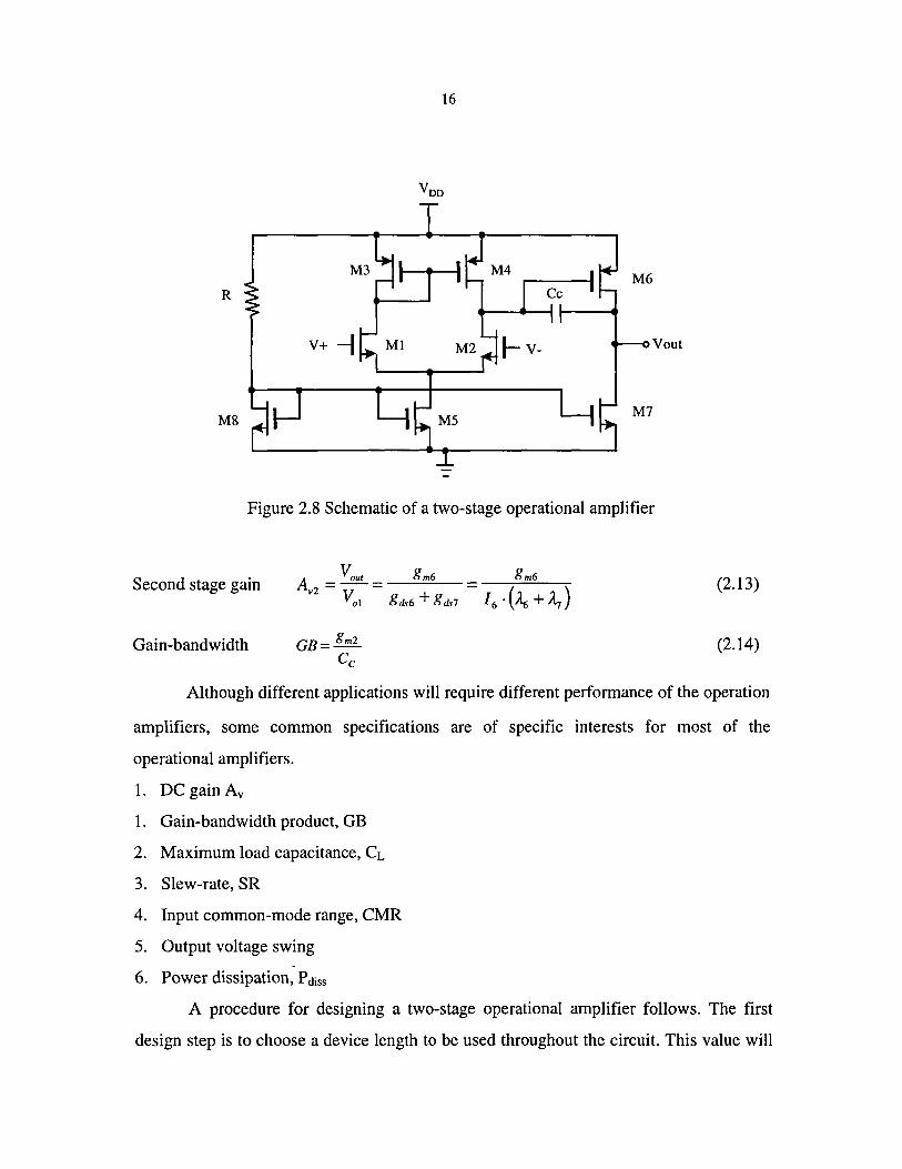
16
M3 M4 M6
R
I- v- Vout
M8 M7
Figure 2.8 Schematic of a two-stage operational amplifier
Second stage gain
Gain-bandwidth GB= gm2
Cc
(2.13)
(2.14)
Although different applications will require different performance of the operation
amplifiers, some common specifications are of specific interests for most of the
operational amplifiers.
1. DC gain Av
1. Gain-bandwidth product, GB
2. Maximum load capacitance, CL
3. Slew-rate, SR
4. Input common-mode range, CMR
5. Output voltage swing .
6. Power dissipation, P diss
A procedure for designing a two-stage operational amplifier follows. The first
design step is to choose a device length to be used throughout the circuit. This value will
17
detennine the value of channel length modulation parameter A, which is a critical
parameter in the calculation of the amplifier gain.
The next design step is to detennine the value of the compensation capacitor Ce. It
was known that in two pole systems, in order to obtain a 60° phase margin, the second
pole has to be beyond 2.2 times of the unit gain bandwidth GB. It was shown that such
pole requirement will result in the minimum value for the compensation capacitor
[AH87].
Cc~0.22· CL (2.15)
For the certain application, CL is known, hence the compensation capacitor can be easily
obtained.
The following step in the design is to detennine the tail current Is. From the
equation (2.13), we can see that the tail current can be obtained based upon the
knowledge of cOI1lpensation capacitor Ce and slew rate requirement,
Is = SR(slewrate)· Cc (2.16)
The tail current is mirrored from the current mirror consisting of transistor Ms andMg,
assume the size of the two transistors are same, the drain current of transistor M8 is
known, acccordingly, the value of the resistor R can be obtained.
R "" V DD - VdratM8
Is (2.17)
The size of the M2 can be detennined by using the requirement for the unit gain
bandwidth.
(2.18)
(2.19)
With Cc and I DS2 = I DS;1, available, solving the above equations gives the ratio of
(%)2' Since Ml and M2 are matched, (~)l is also obtained.
18
In order to make the zero due to the Miller compensation larger than the second
pole, we choose / DS6 = / DS7 = 5 . / DS2 = 5 . / DSI' since / DSI = / DS2 = / DSj{, we can easily
obtain the size of the M7.
(2.20)
Using the equation for the DC gain
(2.21)
we can solve the size of M6 since we have all of other parameters used in this equation.
The final parameter to be solved is the size of M3 and M4. If we force the V GS3 to
be equal to V Gs~[GA90], following equation has to be met.
(2.22)
Since / DS3 = / DS4 = / DSj{ , the above equation becomes,
(W) = (o/zl.~ L 3 2 /6
(2.23)
Since M4 and M3 are matched, the size of M4 is also obtained.
In the above discussion, we chose one specification to determine relevant
parameters at each design step. However, other specifications must be checked at each
design step. If some of the specifications haven't been met, adjustments must be made to
insure all specifications have been met.
19
CHAPTER 3. LOW-VOLTAGE OPERATIONAL AMPLIFIER
DESIGN
In Chapter 2, some basic knowledge of the MOSFET and design procedures for
two-stage operational amplifiers were introduced. In this chapter, design details of a
500mV low-voltage operational amplifier will be discussed. I will begin with reviewing
previous work regarding low-voltage operational amplifiers design, followed by an
introduction of the proposed structure for 500m V low-voltage operational amplifier.
3.1 Previous work
Many papers and books have been published on low-voltage operational
amplifiers [EC96] [FM89] [HL85] [AB95]. With reduced power supply voltage, many
operational amplifier architectures will lose operational range especially at their input
stages. Thus operational amplifiers with large input signal swing are greatly desired. Such
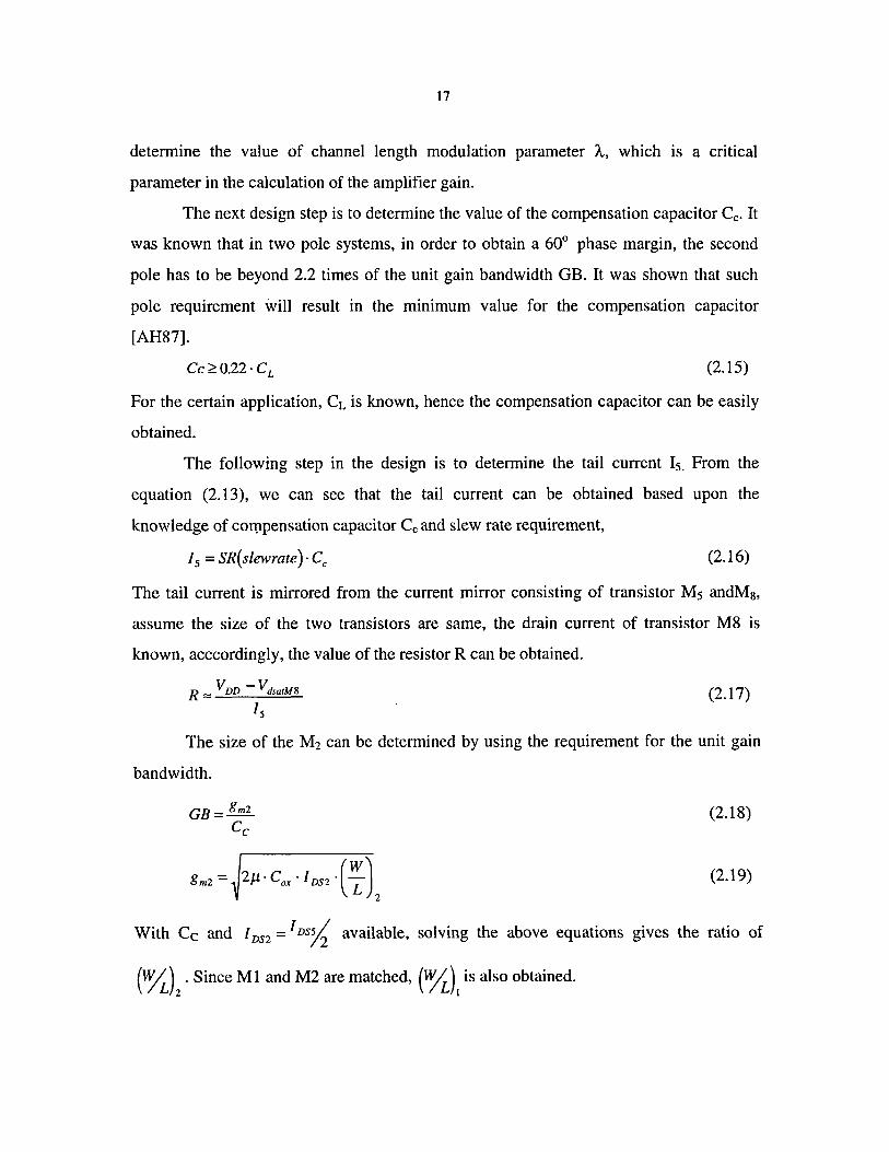
operational amplifiers often employed complementary differential pairs as an input stage
as shown in Figure 3.1 [SI95], [HL85].
v"
Figure 3.1 Complementary differential input stage
20
By connecting an n-channel differential pair and a p-channel differential pair in
parallel, the input stage can reach rail-to-rail. When the common mode voltage, VeM• is
near the negative power supply voltage, only the p-channel pair is functional. When the
common mode voltage, V CM. is near the positive power supply voltage, only the n-channel
pair is functional. When V CM is intennediate between the negative supply and positive
supply, both the n-channel pair and p-channel pair will operate. An important design
consideration associated with this kind of circuit is to keep the sum of transconductances
of the comElementary differential pairs (gm = gmn + gmp) constant in order to guarantee a
co_ostanLgain-bandwidth product under different common-mode input voltages. The
methods to keep gm constant can be found in Satoshi Sakurai's work [SI95].
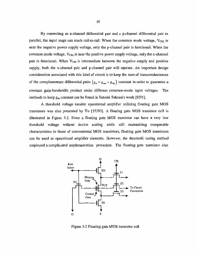
A threshold voltage tunable operational amplifier utilizing floating gate MOS
transistors was also presented by Yu [YU93]. A floating gate MOS transistor cell is
illustrated in Figure 3.2. Since a floating gate MOS transistor can have a very low
threshold voltage without device scaling while still maintaining comparable
characteristics to those of conventional MOS transistors, floating gate MOS transistors
can be used as operational amplifier elements. However, the threshold tuning method
employed a complicated implementation procedure. The floating gate transistor also
Row Select
G
D
s
CE
To Circuit Connection
Figure 3.2 Floating gate MOS transistor cell
21
does not compensate for temperature variation. Most importantly, the floating gate device
requires specified processing steps that are normally not available in most of existing
standard commercial semiconductor processes.
3.2 Threshold voltage tuning
Generally, the threshold voltage and the saturation voltage of MOS transistors for
operation in the strong inversion region limits the minimum supply voltage. This
limitation is given by the expression,
(3.1)
For a current standard CMOS technology, this limitation will result in a minimum supply
voltage of approximately I.5V [MU96].
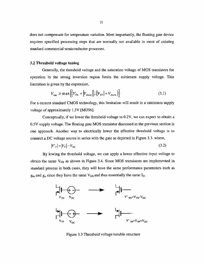
Conceptually, if we lower the threshold voltage to O.2V, we can expect to obtain a
O.5V supply voltage. The floating gate MOS transistor discussed in the previous section is
one approach. Another way to electrically lower the effective threshold voltage is to
connect a DC voltage source in series with the gate as depicted in Figure 3.3. where,
(3.2)
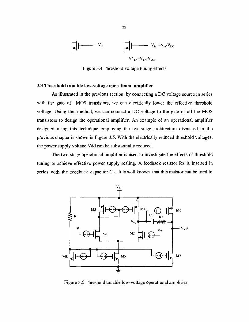
By lowing the threshold voltage, we can apply a lower effective input voltage to
obtain the same V GS as shown in Figure 3.4. Since MOS transistors are implemented in
standard process in both cases, they will have the same performance parameters such as
gm and go since they have the same V GS and thus essentially the same ID.
~II---V· TP=vTP+voc
Figure 3.3 Threshold voltage tunable structure
22
~I---I ~II---
Figure 3.4 Threshold voltage tuning effects
3.3 Threshold tunable low-voltage operational amplifier
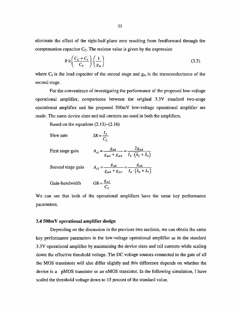
As illustrated in the previous section, by connecting a DC voltage source in series
with the gate of MOS transistors, we can electrically lower the effective threshold
voltage. Using this method, we can connect a DC voltage to the gate of all the MOS
transistors to design the operational amplifier. An example of an operational amplifier
designed using this technique employing the two-stage architecture discussed in the
previous chapter is shown in Figure 3.5. With the electrically reduced threshold voltages,
the power supply voltage Vdd can be substantially reduced.
The two-stage operational amplifier is used to investigate the effects of threshold
tuning to achieve effective power supply scaling. A feedback resistor Rz is inserted in
series with the feedback capacitor Ce. It is well known that this resistor can be used to
M3 M6
R
V- Vout
-B--I
M8 M5 M7
Figure 3.5 Threshold tunable low-voltage operational amplifier
23
eliminate the effect of the right-half-plane zero resulting from feedforward through the
compensation capacitor Ce. The resistor value is given by the expression
(3.3)
where CI is the load capacitor of the second stage and gm is the transconductance of the
second stage.
For the convenience of investigating the performance of the proposed low-voltage
operational amplifier, comparisons between the original 3.3V standard two-stage
operational amplifier and the proposed 500m V low-voltage operational amplifier are
made. The same device sizes and tail currents are used in both the amplifiers.
Based on the equations (2.13)-(2.16)
Slew rate
First stage gain
Second stage gain
Gain-bandwidth
SR=~ Cc
Av2 = _....;;.g..:;.;m.:;.,..6 -
gds6 + gds7
GB= gm2
Cc
We can see that both of the operational amplifiers have the same key performance
parameters.
3.4 50 Om V operational amplifier design
Depending on the discussion in the previous two sections, we can obtain the same
key performance parameters in the low-voltage operational amplifier as in the standard
3.3V operational amplifier by maintaining the device sizes and tail currents while scaling
down the effective threshold voltage. The DC voltage sources connected to the gate of all
the MaS transistors will also differ slightly and this difference depends on whether the
device is a pMOS transistor or an nMOS transistor. In the following simulation, I have
scaled the threshold voltage down to 15 percent of the standard value.
24
The device sizes used in the simulation are given in Table 2.1. These sizes were
determined by following the procedure given in Chapter 2.
Level 13 0.5~ CMOS models were used in the simulation. Although the minimum
size used in the design is 2~, due to available MOSIS HP technologies and fabrication
schedule, the circuit was supposed to fabricated in 0.5~ CMOS process. However, level 3
0.5~ CMOS models were also used in simulation for comparison purpose.
Table 3.1 Device sizes used in the two-stage operational amplifier
M1 M2 M3 M4 M5 M6 M7 M8 15 Rz Cc
W(~) 20 20 80 80 20 398 48 20 20~A 12K 2P
L(~) 2 2 2 2 2 2 2 2
Figure 3.6 shows the frequency response of the original 3.3V two-stage
operational amplifier operating at T=250C, (a) shows the magnitude response while (b)
shows phase response. In order to have 20uA tail current, the biasing resistor R is equal to
R z VDD - VT z 3.3 - 0.8 125K 18 20
(3.4)
Figure 3.7 shows the preliminary frequency response of the proposed 500mV low
voltage operational amplifier also operating at T=25°C. (a) shows the magnitude response
and (b) shows phase response. In order to provide the same tail current, the biasing
resistor R in the 500m V design is
R z V DD - V T z 05 - 0.15 z 17 K 18 20
(3.5)
From comparisons between Figure 3.6 and Figure 3.7, we can see that the
proposed 500m V low-voltage amplifier has comparable magnitude and phase
performance to that of the original 3.3V structure. The original 3.3V operational amplifier
demonstrates 75dB DC gain, lOMHz unity gain bandwidth and a 60° phase margin. The
proposed 500mV low-voltage operational amplifier achieves 70dB DC gain, 8MHz unity
gain bandwidth and a 62° phase margin.
25
Magnitude AC Response
90.0 5: lout
-30_
-70.
Phase
200. 5: lout
~" "',
(a)
AC Response
\
130.
60.0
\ \ \ \ \ \ \
\
\''s...
---+--", \
\ \ , \ , \ , \ \ , l
" '.
109 freauenr:v
-10.0L_-::: ____ --L-=-____ -1--::--_->' ___ _
100 103 106 109 frequency
(b)
Figure 3.6 Frequency response of the original two-stage operational amplifier
(a) Magnitude response (b) Phase response
26
Magnitude 90.0
AC Response
-30.
-70.
Phase 200.
130.
60.0
§: lout
§: lout
~ , , \ \
(a)
AC Response
\ \ \
\ \
\ , ''i.,.
--~ ~" , \ \ ,
I , " I I \ . I l I . \ .
10 9 frequency
-10.0~ ________ ~~ ________ ~~ __ ~\ ____ _
10 0 10 3 106 10 9 frequency
(b)
Figure 3.7 Frequency response of the proposed 500mV low-voltage operational amplifier
(a) Magnitude response (b) Phase response
27
3.5 DC voltage source
Ideal DC voltage sources were connected to the gate of MOS transistors in the
preliminary simulation. However, these DC voltage sources are implemented with
capacitors charged periodically to keep the voltage on the capacitors constant. Figure 3.8
shows the basic approach for this implementation.
~ In ~~L Out
0 0
<1>1 C <1>1
(a)
r---{- +)------,
MS3 MS4
c M
Vss
(b)
Figure 3.8 DC voltage source (a) Symbol (b) Circuit implementation
Figure 3.8 (a) shows the DC voltage representation. Figure 3.8 (b) shows a circuit
implementation. Signals <\>1 and <\>2 are two phase nonoverlapping clocks. During <\>2, the
reference voltage will charge the capacitor C to VDC• During <\>1, the capacitor charged to
VDC will be connected to the gate of MOSFET M in the operational amplifier circuit and
works as the DC voltage source in Figure 3.5. Since the input resistance of MOS
transistors is very large, the charge on the capacitor C can be maintained for a log time.
The nonideal effects of limited time storage of charge on C must nonetheless be
investigated. To investigate these effects, consider the capacitor in series with the gate of
28
M6 of Figure 3.5. Figure 3.9 shows this capacitor along with the small-signal loading
impressed by the preceeding and following stages. In Figure 3.9, the components are
defined by
R-1 R-1 R-1 1 = ds2 + ds4
R 2= R;n6
C2 = Cgs6
C +
M6
Figure 3.9 DC effects in the switched capacitor circuits
(3.6)
(3.7)
(3.8)
(3.9)
Rin6 is the input impedance of the MaS transistor M6, which is of the order of 1010 and is
much larger than RI• Assuming capacitor C is much larger than CI and C2, the time
constant of the above circuit is about
'r::::: R;n . C::::: 5x lOto x5x 10-12 = 0.25S (3.1)
That means charge on the capacitor can be kept for a long time so that the frequency of CPI
and c1>2 can be very low. On the other hand capacitor C charging is very fast, so that c1>2
can be a pulse. The typical signal waveforms for CPI and c1>2 are shown in Figure 3.10.
u u U _-----InL------Inl----~n'____
Figure 3.10 Waveform for CPI and <l>2
29
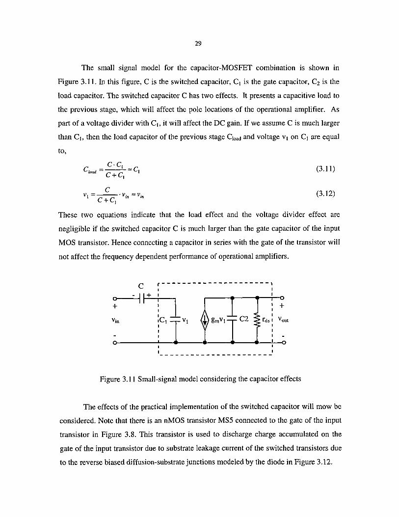
The small signal model for the capacitor-MOSFET combination is shown in
Figure 3.11. In this figure, C is the switched capacitor, CI is the gate capacitor, C2 is the
load capacitor. The switched capacitor C has two effects. It presents a capacitive load to
the previous stage, which will affect the pole locations of the operational amplifier. As
part of a voltage divider with C I , it will affect the DC gain. If we assume C is much larger
than CI, then the load capacitor of the previous stage Cload and voltage VI on CI are equal
to,
c·c) C1d = =C)
oa c+c )
(3.11)
(3.12)
These two equations indicate that the load effect and the voltage divider effect are
negligible if the switched capacitor C is much larger than the gate capacitor of the input
MOS transistor. Hence connecting a capacitor in series with the gate of the transistor will
not affect the frequency dependent performance of operational amplifiers.
r---------------------, C I I
~---II~ ICt Vt C2 I
I + I I
rds I Vout I I
Figure 3.11 Small-signal model considering the capacitor effects
The effects of the practical implementation of the switched capacitor will mow be
considered. Note that there is an nMOS transistor MS5 connected to the gate of the input
transistor in Figure 3.8. This transistor is used to discharge charge accumulated on the
gate of the input transistor due to substrate leakage current of the switched transistors due
to the reverse biased diffusion-substrate junctions modeled by the diode in Figure 3.12.
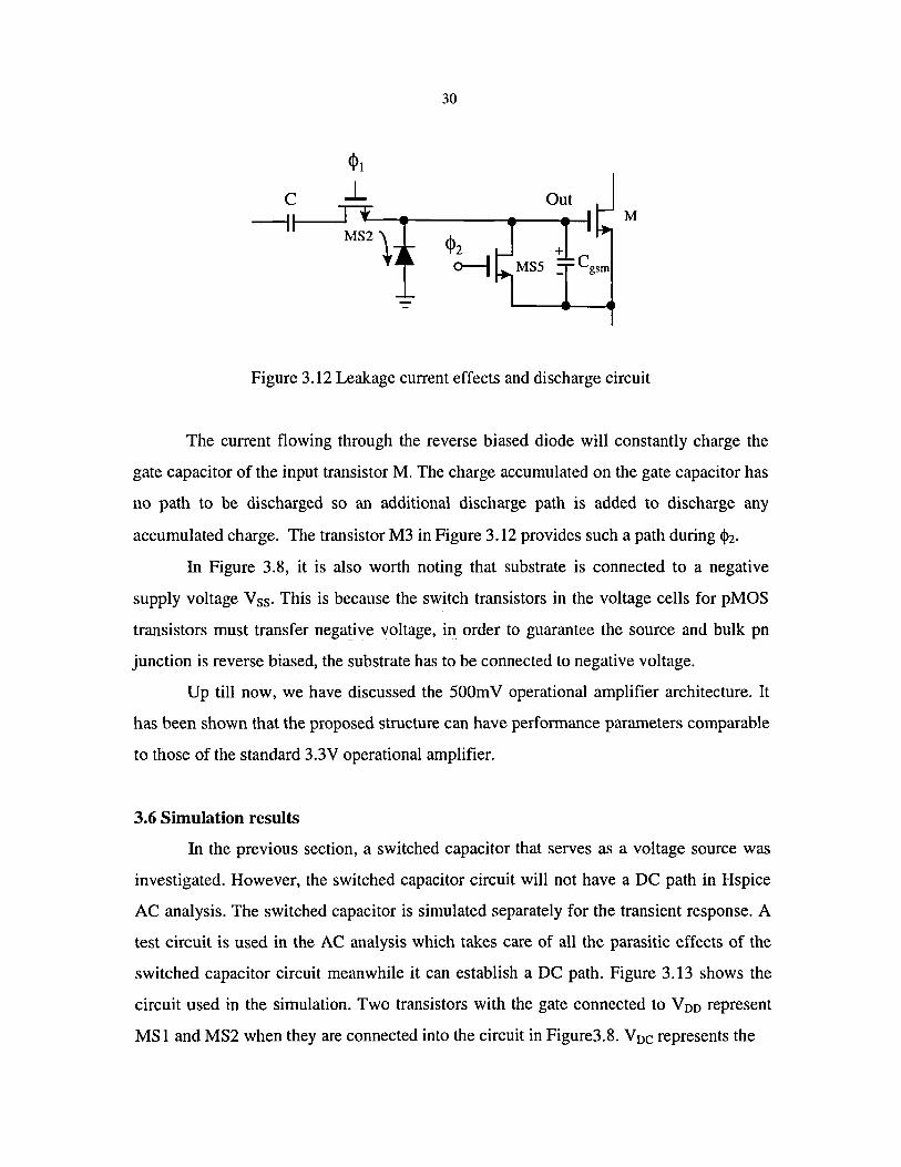
30
<1>1
..L M
Figure 3.12 Leakage current effects and discharge circuit
The current flowing through the reverse biased diode will constantly charge the
gate capacitor of the input transistor M. The charge accumulated on the gate capacitor has
no path to be discharged so an additional discharge path is added to discharge any
accumulated charge. The transistor M3 in Figure 3.12 provides such a path during <1>2.
In Figure 3.8, it is also worth noting that substrate is connected to a negative
supply voltage V ss. This is because the switch transistors in the voltage cells for pMOS
transistors must transfer negative voltage, in order to guarantee the source and bulk pn
junction is reverse biased, the substrate has to be connected to negative voltage.
Up till now, we have discussed the 500m V operational amplifier architecture. It
has been shown that the proposed structure can have performance parameters comparable
to those of the standard 3.3V operational amplifier.
3.6 Simulation results
In the previous section, a switched capacitor that serves as a voltage source was
investigated. However, the switched capacitor circuit will not have a DC path in Hspice
AC analysis. The switched capacitor is simulated separately for the transient response. A
test circuit is used in the AC analysis which takes care of all the parasitic effects of the
switched capacitor circuit meanwhile it can establish a DC path. Figure 3.13 shows the
circuit used in the simulation. Two transistors with the gate connected to Voo represent
MS 1 and MS2 when they are connected into the circuit in Figure3.8. Voc represents the
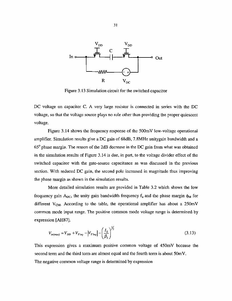
31
VDD VDD
I C I In 00--------.-1 :: I ~~O Out
R VDC
Figure 3.13 Simulation circuit for the switched capacitor
DC voltage on capacitor C. A very large resistor is connected in series with the DC
voltage, so that the voltage source plays no role other than providing the proper quiescent
voltage.
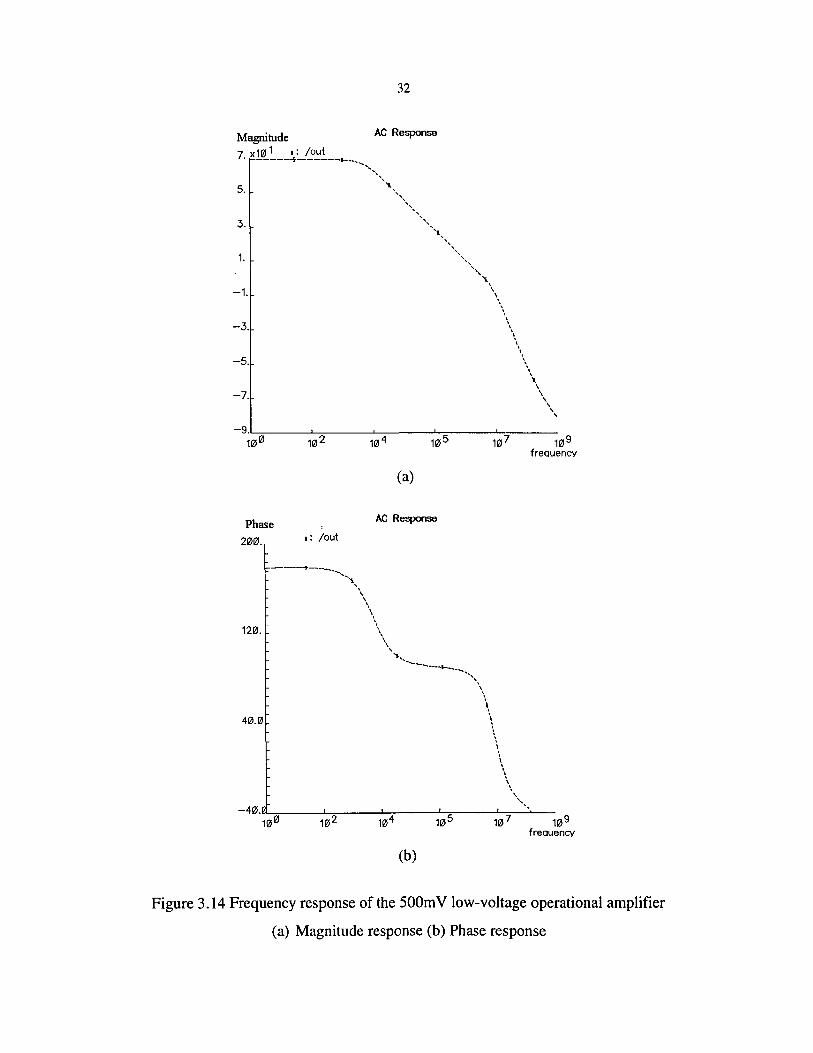
Figure 3.14 shows the frequency response of the 500mV low-voltage operational
amplifier. Simulation results give a DC gain of 68dB, 7.8MHz unitygain bandwidth and a
65° phase margin. The reason of the 2dB decrease in the DC gain from what was obtained
in the simulation results of Figure 3.14 is due, in part, to the voltage divider effect of the
switched capacitor with the gate-source capacitance as was discussed in the previous
section. With reduced DC gain, the second pole increased in magnitude thus improving
the phase margin as shown in the simulation results.
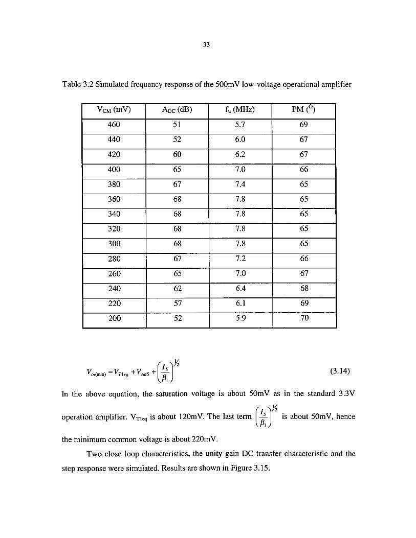
More detailed simulation results are provided in Table 3.2 which shows the low
frequency gain ADc, the unity gain bandwidth frequency fu and the phase margin <PM for
different V CM. According to the table, the operational amplifier has about a 250m V
common mode input range. The positive common mode voltage range is determined by
expression [AH87].
(3.13)
This expression gives a maximum positive common voltage of 450m V because the
second term and the third term are almost equal and the fourth term is about 50mV.
The negative common voltage range is determined by expression
32
AC Response
3.
1.
-1.
-3.
-5.
-7.
-9. 10 0 10 2 10 4 105 107 10 9
freauency
(a)
Phase AC Response
200. ,: lout
(b)
Figure 3.14 Frequency response of the 500mV low-voltage operational amplifier
(a) Magnitude response (b) Phase response
33
Table 3.2 Simulated frequency response of the 500m V low-voltage operational amplifier
VCM (mV) ADC (dB) fu (MHz) PM (0)
460 51 5.7 69
440 52 6.0 67
420 60 6.2 67
400 65 7.0 66
380 67 7.4 65
360 68 7.8 65
340 68 7.8 65
320 68 7.8 65
300 68 7.8 65
280 67 7.2 66
260 65 7.0 67
240 62 6.4 68
220 57 6.1 69
200 52 5.9 70
(I ),x
Vin(min) = V Tleq + V sat5 + A (3.14)
In the above equation, the saturation voltage is about 50mV as in the standard 3.3V
operation amplifier. VTI<q is about 120mV. The last teno (i,)!1 is about 50mV, hence
the minimum common voltage is about 220mV.
Two close loop characteristics, the unity gain DC transfer characteristic and the
step response were simulated. Results are shown in Figure 3.15.
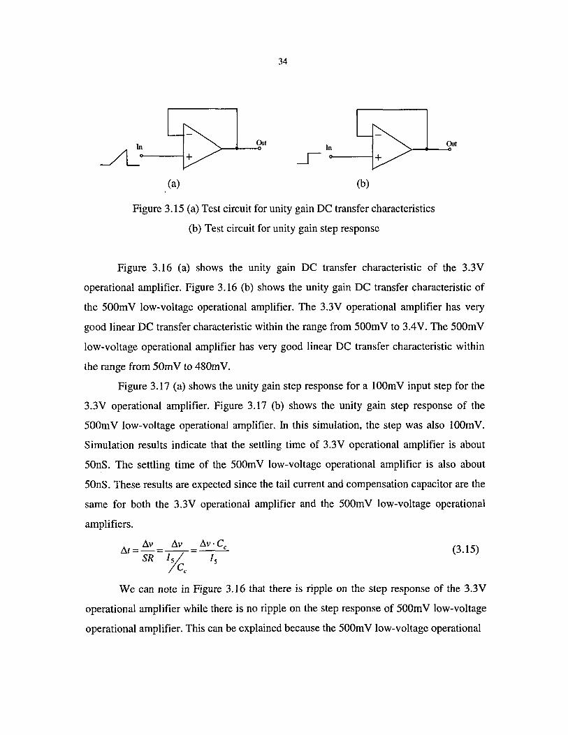
34
Ao----;+ CM
(a)
In
~
(b)
OJ! >-_--0
Figure 3.15 (a) Test circuit for unity gain DC transfer characteristics
(b) Test circuit for unity gain step response
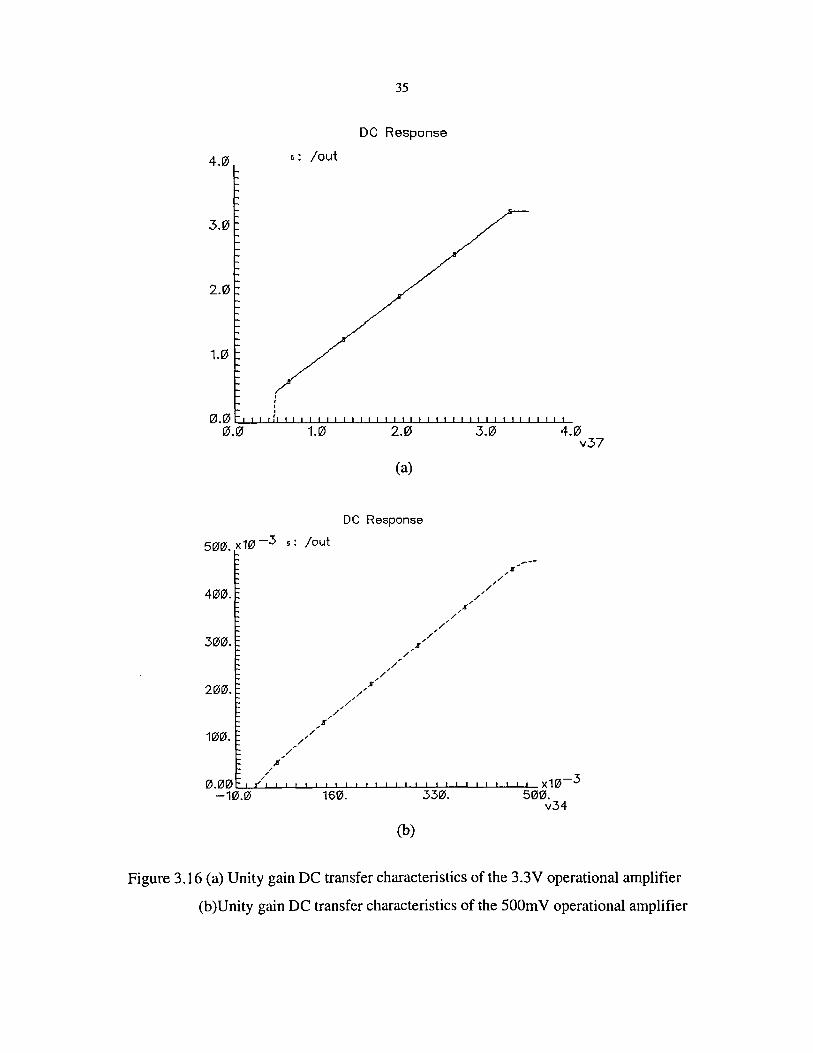
Figure 3.16 (a) shows the unity gain DC transfer characteristic of the 3.3V
operational amplifier. Figure 3.16 (b) shows the unity gain DC transfer characteristic of
the 500m V low-voltage operational amplifier. The 3.3V operational amplifier has very
good linear DC transfer characteristic within the range from 500mV to 3.4V. The 500mV
low-voltage operational amplifier has very good linear DC transfer characteristic within
the range from 50mV to 480mV.
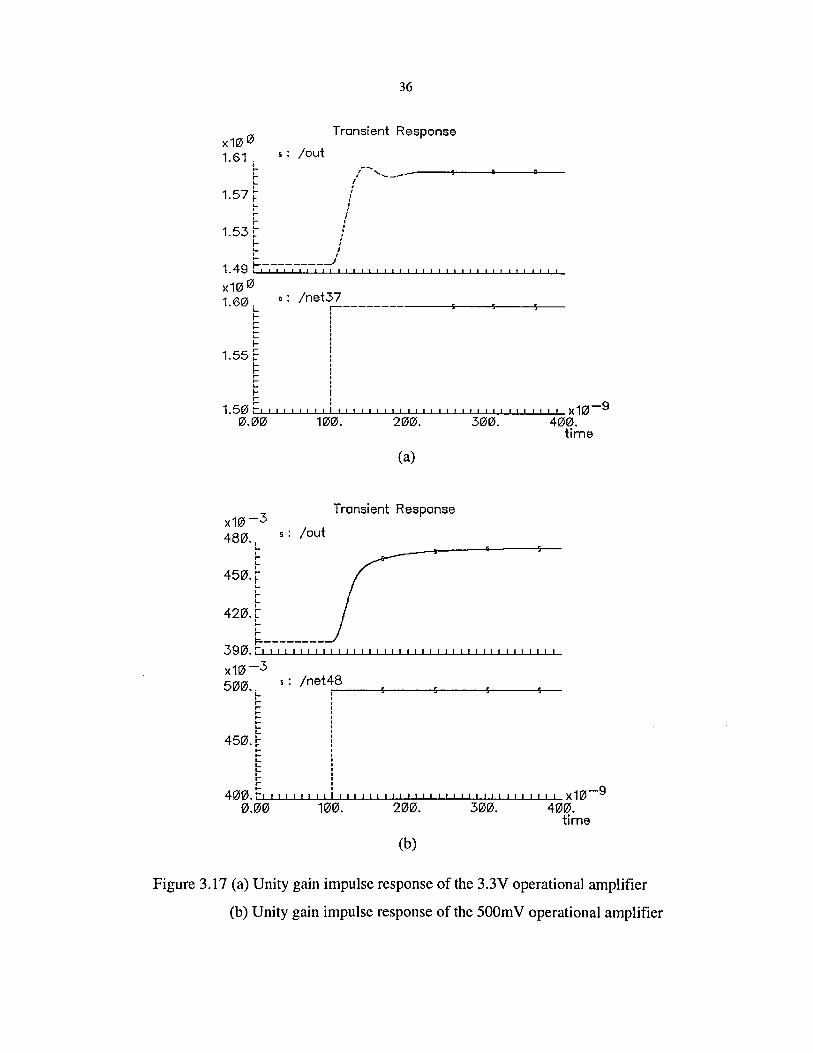
Figure 3.17 (a) shows the unity gain step response for a 100mV input step for the
3.3V operational amplifier. Figure 3.17 (b) shows the unity gain step response of the
500m V low-voltage operational amplifier. In this simulation, the step was also 100m V.
Simulation results indicate that the settling time of 3.3V operational amplifier is about
50nS. The settling time of the 500mV low-voltage operational amplifier is also about
50nS. These results are expected since the tail current and compensation capacitor are the
same for both the 3.3V operational amplifier and the 500mV low-voltage operational
amplifiers.
I1t= I1v =~= I1v· Cc
SR 15/ Is ICc
(3.15)
We can note in Figure 3.16 that there is ripple on the step response of the 3.3V
operational amplifier while there is no ripple on the step response of 500m V low-voltage
operational amplifier. This can be explained because the 500m V low-voltage operational
35
DC Response
4.10 ~: lout
3.10
2.10
1.10
(a)
DC Response
51010. x110 -3 5: lout
(b)
Figure 3.16 (a) Unity gain DC transfer characteristics of the 3.3V operational amplifier
(b )Unity gain DC transfer characteristics of the 500m V operational amplifier
36
x10 0 Transient Response
1.61 ; ~: lout ~ -~ t ,/ ,----
1.57 t / ~ l
1~53 t 1 I- , L. I , , t.. ________ -'
1.49 r, 1 , , , I I I I t I' , , I , I I I I I I I , I "" , , I
x10 0 1.60.
L.
~ I-
1.55r ~ ... ~ L.
t-
~: Inet37 r---, : :
I i
~ : 1.50:-, r I I I I I I I I I I ! r I I I I I I I I I I I I I I I I I I
0.00 100. 200. 300.
x10-3
480., ... , ... L.
450.[ L. I-L.
420.[ I-
(a)
Transient Response
~: lout
I I I
I I I
I I I I
I I I I x10-9 400.
time
~--------3910 .. ;1 I I I I I I I I I I I I I I I I I I I I I I I I I I I I I I I I I I I I I I
x10-3 51010.. ~: /net4;-8 __ +--_~r--_-+-__ -+-_
~ ... ~ ~ ... L. L
451O.~ ~ ... L. L
~ ... 400 .. F, 11 I I r I I I I 11111 I I I III I I I I I I I III
10.1010 11010. 21010. 31010.
(b)
I I I I I I I x11O-9 41010.
time
Figure 3.17 (a) Unity gain impulse response of the 3.3V operational amplifier
(b) Unity gain impulse response of the 500mV operational amplifier
37
amplifier has a larger phase margin than the 3.3V operational amplifier. A modest
reduction in the compensation capacitor for the 500m V operational amplifier should
provide some improvement in the settling time.
3.7 Conclusions
A 500m V low-voltage operational amplifier design was investigated in this
chapter. A circuit implementation was presented and parasitic effects are considered.
Simulations results indicated that the 500m V low-voltage amplifier has comparable key
performance parameters to a 3.3V operational amplifier as can be seen from the
summarizes in Table 3.3.
Table 3.3 Comparisons of performance parameters of the two operational amplifiers
Standard Proposed
amplifier amplifier
Supply voltage 3.3V 0.5V
DC-gain 75dB 68dB
GBW 10MHz 7.8MHz
PM 60° 65°
Tail current 20JlA 20JlA
Power dissipation 200JlW 35JlW
As anticipated, simulation results also indicated that these two operational
amplifiers have similar unity gain close loop performance. Although the 500m V low
voltage operational amplifier has a much smaller common mode input range, it is still
reasonable for such a low supply voltage.
Figure 3.18 shows the layout of the 500m V low-voltage operational amplifier core
and the switched capacitor voltage sources. This layout was done in a 0.5Jl CMOS
process.
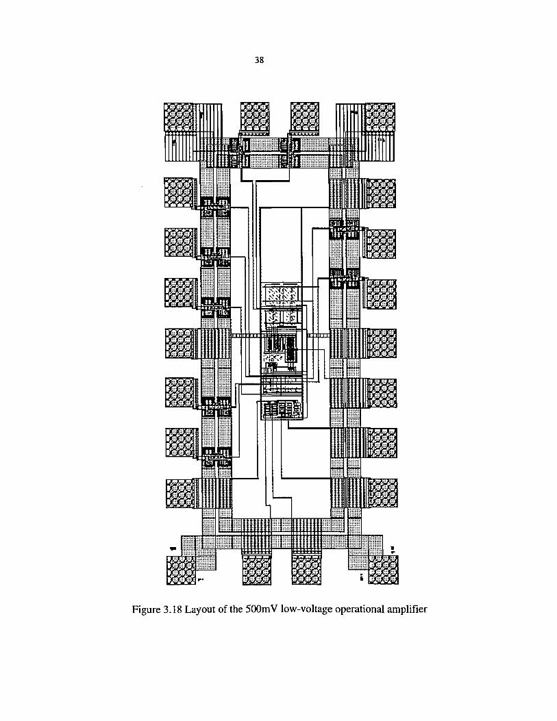
38
Figure 3.18 Layout of the 500mV low-voltage operational amplifier
39
CHAPTER 4. SUPPLEMENTARY CIRCUIT
IMPLEMENTATIONS
In Chapter 3, we discussed the design of the 500mV low-voltage operational
amplifier. Methods for generating the negative voltage V ss, for determining the voltage
V DC that is stored on the series capacitor C and generation of the clocks <1>1 and <\>2 were
not considered. In this chapter, the supplementary circuits need to realize these functions
for the low-voltage operational amplifier will be given.
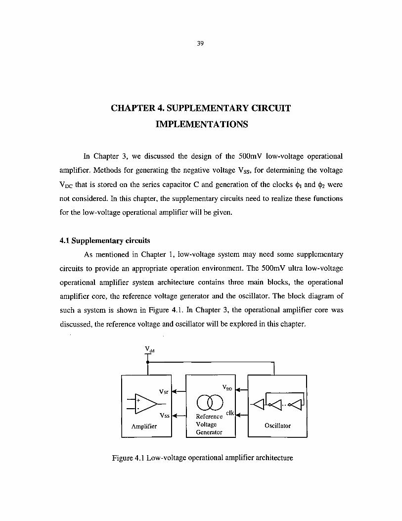
4.1 Supplementary circuits
As mentioned in Chapter 1, low-voltage system may need some supplementary
circuits to provide an appropriate operation environment. The 500mV ultra low-voltage
operational amplifier system architecture contains three main blocks, the operational
amplifier core, the reference voltage generator and the oscillator. The block diagram of
such a system is shown in Figure 4.1. In Chapter 3, the operational amplifier core was
discussed, the reference voltage and oscillator will be explored in this chapter.
-
I
~' ..- VDD ~
ODclk -4<].·<}J Vss +- Reference ~
Amplifier Voltage Oscillator Generator
Figure 4.1 Low-voltage operational amplifier architecture
40
The reference voltage generator provides the DC voltage source and the negative
supply voltage for the operational amplifier. The oscillator provides clocks for the
switched capacitors and the charge pump which pumps the 500m V supply voltage up to
3.3V. The 3.3V supply is needed to extract the reference DC voltage. Throughout the
text, VDD refers to 3.3V supply voltage and Vdd refers to 500mV supply voltage.
4.2 Reference voltage generation
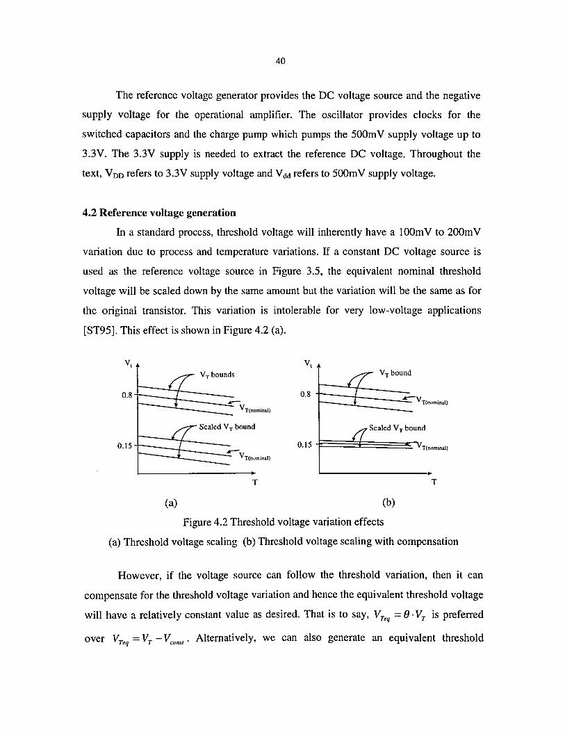
In a standard process, threshold voltage will inherently have a 100m V to 200m V
variation due to process and temperature variations. If a constant DC voltage source is
used as the reference voltage source in Figure 3.5, the equivalent nominal threshold
voltage will be scaled down by the same amount but the variation will be the same as for
the original transistor. This variation is intolerable for very low-voltage applications
[ST95]. This effect is shown in Figure 4.2 (a).
vT bounds vT bound
0,8 -C:---1---= _ V T(nominal)
0,8 L--jL-__ ~ I--l~ ___ -=-VT(nominal)
Scaled V T bound Scaled V T bound
O,151:=_-t ___ ~_ V T(nominal)
0,15 -F===t:===~~ T(nominal)
T T
(a) (b)
Figure 4.2 Threshold voltage variation effects
(a) Threshold voltage scaling (b) Threshold voltage scaling with compensation
However, if the voltage source can follow the threshold variation, then it can
compensate for the threshold voltage variation and hence the equivalent threshold voltage
will have a relatively constant value as desired. That is to say, VTeq = e· VT is preferred
over VTeq
= VT - Vconst • Alternatively, we can also generate an equivalent threshold
41
voltage that is independent of Vr. The desired threshold scaling is shown in Figure 4.2
(b). Both approaches will be considered.
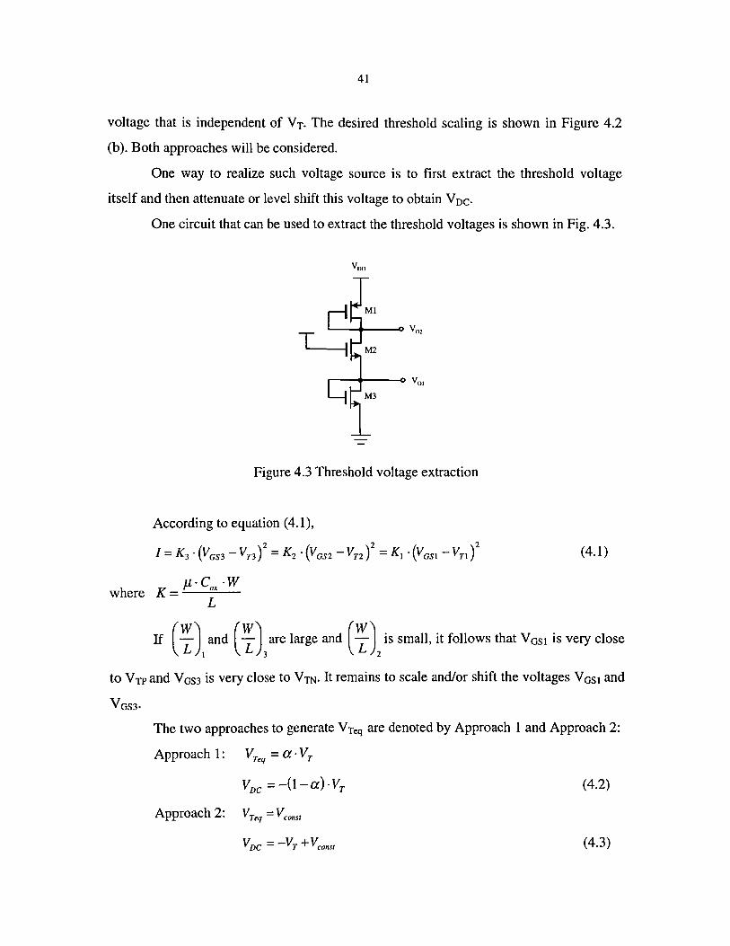
One way to realize such voltage source is to first extract the threshold voltage
itself and then attenuate or level shift this voltage to obtain V DC.
One circuit that can be used to extract the threshold voltages is shown in Fig. 4.3.
T
Figure 4.3 Threshold voltage extraction
According to equation (4.1),
1= K3 . (VGS3 - Vn )2 = K2 . (VGS2 - VT2 )2 = K) . (VGS) - Vn )2 (4.1)
P·e ·w where K = ox
L
If (:). and (:) 3 are large and (:), is small, it follows that VOS! is very close
to VTP and V OS3 is very close to VTN• It remains to scale and/or shift the voltages V OSI and
VOS3•
The two approaches to generate V Teq are denoted by Approach 1 and Approach 2:
Approach 1: V =a·V Teq T
(4.2)
Approach 2: VTeq = Vconsl
(4.3)
42
In Approach 1, the equivalent threshold voltage is a portion of the original
threshold voltage, so that the threshold voltage maintains the same relative variation as
the original one. In Approach 2, the threshold voltage variation is eliminated and the
equivalent threshold voltage is a constant voltage. Both approaches will be discussed
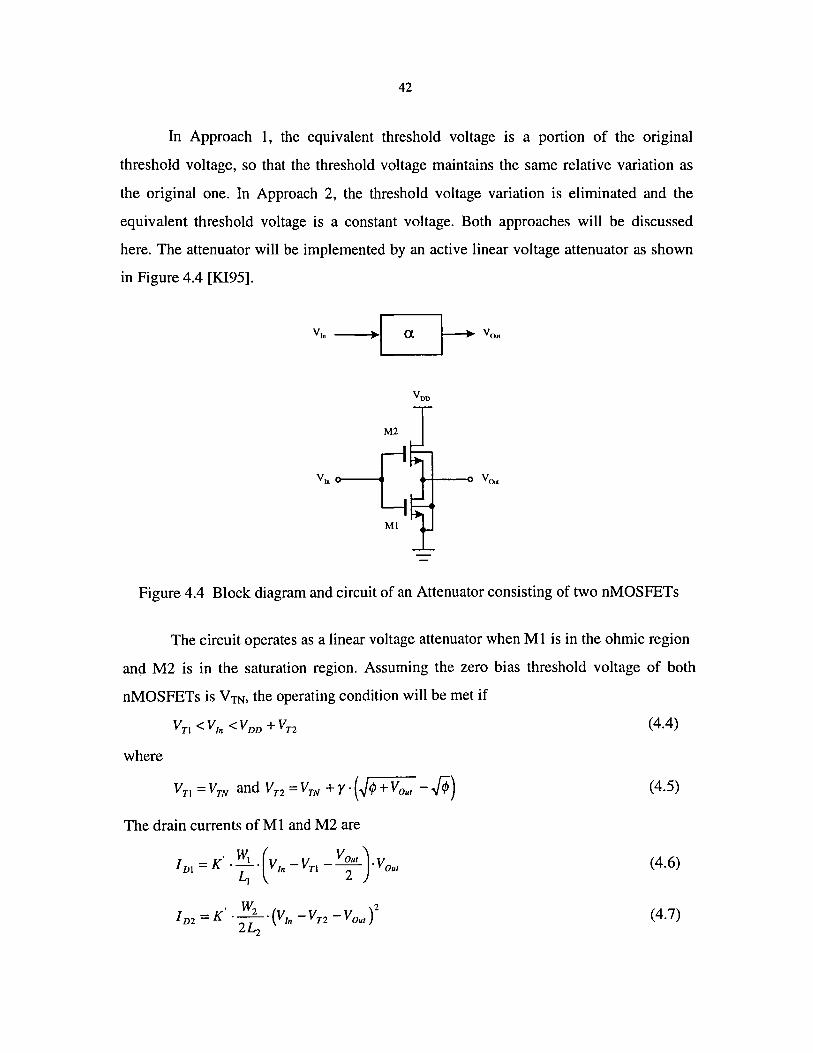
here. The attenuator will be implemented by an active linear voltage attenuator as shown
in Figure 4.4 [KJ95].
M2
...-r--o VOul
Ml
Figure 4.4 Block diagram and circuit of an Attenuator consisting of two nMOSFETs
The circuit operates as a linear voltage attenuator when M 1 is in the ohmic region
and M2 is in the saturation region. Assuming the zero bias threshold voltage of both
nMOSFETs is VTN, the operating condition will be met if
(4.4)
where
(4.5)
The drain currents of M 1 and M2 are
. WI ( Vout ) V 1m = K '-' YIn -Vn --- . Out LI 2
(4.6)
. W2 ( )2 I D2 = K . --' Vln - V T2 - VOut 2~
(4.7)
43
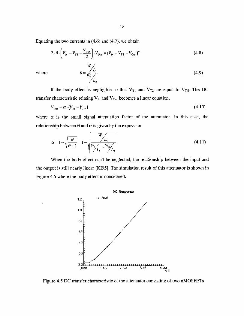
Equating the two currents in (4.6) and (4.7), we obtain
2.e{V1n -Vn - V~ut }Vout = (Vln -Vn -Vout )2
where
(4.8)
(4.9)
If the body effect is negligible so that Vn and VTI are equal to VTN• The DC
transfer characteristic relating YIn and Vout becomes a linear equation,
(4.10)
where ex is the small signal attenuation factor of the attenuator. In this case, the
relationship between e and ex is given by the expression
(4.11)
When the body effect can't be neglected, the relationship between the input and
the output is still nearly linear [KI95]. The simulation result of this attenuator is shown in
Figure 4.5 where the body effect is considered.
1.2 I: lout
1.0
.80
.60
.40
.20
1.45
DC Response
2.30 3.15 4.00 v11
Figure 4.5 DC transfer characteristic of the attenuator consisting of two nMOSFETs
44
The result indicates that the attenuator consisting of two nMOS transistors has
very good linearity within the input range from 1.2V to 3.3V. The attenuator can not be
used to attenuate voltage VTN because VTN < 1.2V . To solve this problem, two types of
attenuators will be used for reasons that become apparent later. Thus consider the
attenuator consisting of two pMOSFETs as shown in Figure 4.6.
Ml
~---o vOu!
M2
Figure 4.6 Block diagram and circuit of an attenuator consisting of two pMOSFETs
Similar to the analysis of the attenuator consisting of two nMOSFETs, the DC
transfer characteristic of this attenuator is,
where
a=l-~I W21 ILl + IL2
(4.12)
(4.13)
The simulation result of this attenuator is shown in Figure 4.7. This attenuator has
very good linear DC transfer characteristic within the range from 0 to 2V.
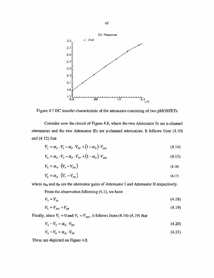
45
DC Re5pon5e
3.3 .: lout
.80 1.6 2.4 v11
Figure 4.7 DC transfer characteristic of the attenuator consisting of two pMOSFETs
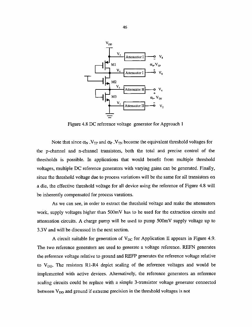
Consider now the circuit of Figure 4.8, where the two Attenuator 1's are n-channel
attenuators and the two Attenuator II's are p-channel attenuators. It follows from (4.10)
and (4.12) that
V2 =ap ,VI -ap ·VTP +(1-ap ),VDD
V4 = a P • V3 - a P • VTP + (1- a P ) • V DD
V6 = aN • (V5 - VTN )
Vs = aN . (V7 - VTN )
(4.14)
(4.15)
(4.16)
(4.17)
where aN and ap are the attenuator gains of Attenuator I and Attenuator II respectively.
From the observation following (4.1), we have
Finally, since VI = 0 and V7 = V DD ' it follows from (4.14)-(4.19) that
V4 -V2 =ap ·VTN
V6 - Vs = aN • VTP
These are depicted on Figure 4.8.
(4.18)
(4.19)
(4.20)
(4.21)
46
T
Figure 4.8 DC reference voltage generator for Approach 1
Note that since aN .VTP and ap .VTN become the equivalent threshold voltages for
the p-channel and n-channel transistors, both the total and precise control of the
thresholds is possible. In applications that would benefit from multiple threshold
voltages, multiple DC reference generators with varying gains can be generated. Finally,
since the threshold voltage due to process variations will be the same for all transistors on
a die, the effective threshold voltage for all device using the reference of Figure 4.8 will
be inherently compensated for process varations.
As we can see, in order to extract the threshold voltage and make the attenuators
work, supply voltages higher than 500mV has to be used for the extraction circuits and
attenuation circuits. A charge pump will be used to pump 500m V supply voltage up to
3.3V and will be discussed in the next section.
A circuit suitable for generation of VDC for Application II appears in Figure 4.9.
The two reference generators are used to generate a voltage reference. REFN generates
the reference voltage relative to ground and REFP generates the reference voltage relative
to VDD• The resistors RI-R4 depict scaling of the reference voltages and would be
implemented with active devices. Alternatively, the reference generators an reference
scaling circuits could be replace with a simple 3-transistor voltage generator connected
between V DD and ground if extreme precision in the threshold voltages is not
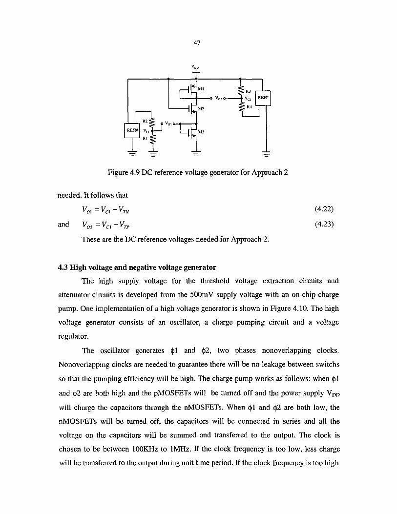
47
Figure 4.9 DC reference voltage generator for Approach 2
needed. It follows that
VOl = VCl - VTN
and V02 = VCl - VTP
These are the DC reference voltages needed for Approach 2.
4.3 High voltage and negative voltage generator
(4.22)
(4.23)
The high supply voltage for the threshold voltage extraction circuits and
attenuator circuits is developed from the 500m V supply voltage with an on-chip charge
pump. One implementation of a high voltage generator is shown in Figure 4.10. The high
voltage generator consists of an oscillator, a charge pumping circuit and a voltage
regulator.
The oscillator generates <1>1 and <1>2, two phases nonoverlapping clocks.
Nonoverlapping clocks are needed to guarantee there will be no leakage between switchs
so that the pumping efficiency will be high. The charge pump works as follows: when <1>1
and <1>2 are both high and the pMOSFETs will be turned off and the power supply VDD
will charge the capacitors through the nMOSFETs. When <1>1 and <1>2 are both low, the
nMOSFETs will be turned off, the capacitors will be connected in series and all the
voltage on the capacitors will be summed and transferred to the output. The clock is
chosen to be between 100KHz to IMHz. If the clock frequency is too low, less charge
will be transferred to the output during unit time period. If the clock frequency is too high
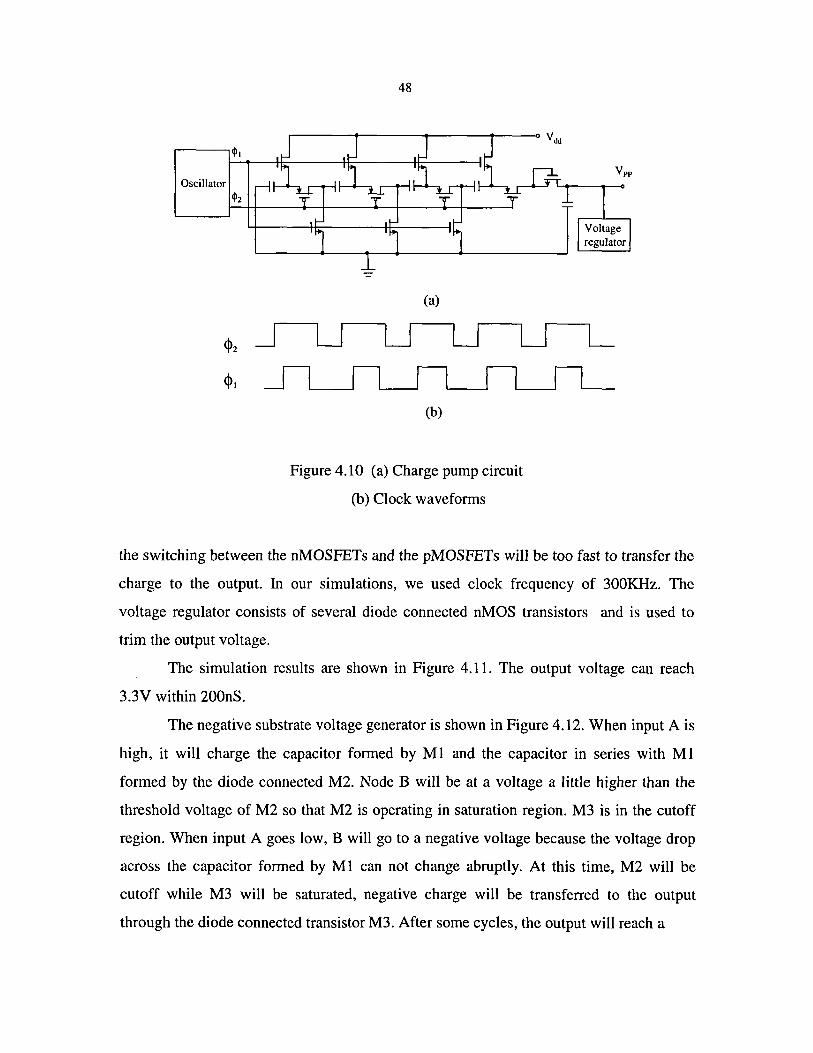
Oscillator $2
48
=
(a)
(b)
Figure 4.10 (a) Charge pump circuit
(b) Clock waveforms
the switching between the nMOSFETs and the pMOSFETs will be too fast to transfer the
charge to the output. In our simulations, we used clock frequency of 300KHz. The
voltage regulator consists of several diode connected nMOS transistors and is used to
trim the output voltage.
The simulation results are shown in Figure 4.11. The output voltage can reach
3.3V within 200nS.
The negative substrate voltage generator is shown in Figure 4.12. When input A is
high, it will charge the capacitor formed by Ml and the capacitor in series with Ml
formed by the diode connected M2. Node B will be at a voltage a little higher than the
threshold voltage of M2 so that M2 is operating in saturation region. M3 is in the cutoff
region. When input A goes low, B will go to a negative voltage because the voltage drop
across the capacitor formed by Ml can not change abruptly. At this time, M2 will be
cutoff while M3 will be saturated, negative charge will be transferred to the output
through the diode connected transistor M3. After some cycles, the output will reach a
4.0
2.0
1.0
49
Transient Response
I: lout
0.0 x1QJ-6 0. 0'-0'-'-'--'-~..L-L....L-2 0-::'-0-::'-. --'--I.-'--''-'-'--'-4-'-0.L...0:'-• ..L-L....L--::'---'--I.-'--'e-00.
time
Figure 4.11 Simulation results for the charge pump
constant negative voltage. Since the input clock voltage level is only from 0 to 1.5V,
using normal nMOS transistors can't generate sufficient negative voltage, floating gate
MOS transistors will be used here. The floating gate MOS transistor can have a lower
threshold voltage than the regular transistors. The floating gate MOSFETs used here are
parasitic-type devices available in any standard process that has double polysilicon layers.
More detailed characteristics about the floating gate MOSFET will be discussed in the
following section.
A
0---11: B
Figure 4.12 Negative substrate voltage generator
50
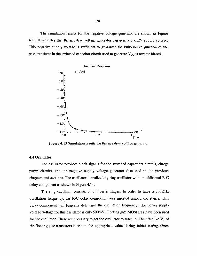
The simulation results for the negative voltage generator are shown in Figure
4.13. It indicates that the negative voltage generator can generate -1.2V supply voltage.
This negative supply voltage is sufficient to guarantee the bulk-source junction of the
pass transistor in the switched capacitor circuit used to generate V DC is reverse biased.
.210
10.10
Transient Response
s: lout
Figure 4.13 Simulation results for the negative voltage generator
4.4 Oscillator
The oscillator provides clock signals for the switched capacitors circuits, charge
pump circuits, and the negative supply voltage generator discussed in the previous
chapters and sections. The oscillator is realized by ring oscillator with an additional R-C
delay component as shown in Figure 4.14.
The ring oscillator consists of 5 inverter stages. In order to have a 300KHz
oscillation frequency, the R-C delay component was inserted among the stages. This
delay component will basically determine the oscillation frequency. The power supply
voltage voltage for this oscillator is only 500mV. Floating gate MOSFETs have been used
for the oscillator. These are necessary to get the oscillator to start up. The effective VT of
the floating gate transistors is set to the appropriate value during initial testing. Since
51
elk
Figure 4.14 Ring oscillator
the floating gate are nonvolatile, they thus retain the charge after they are removed from
the tester.
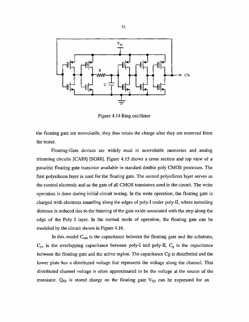
Floating-Gate devices are widely used in nonvolatile memories and analog
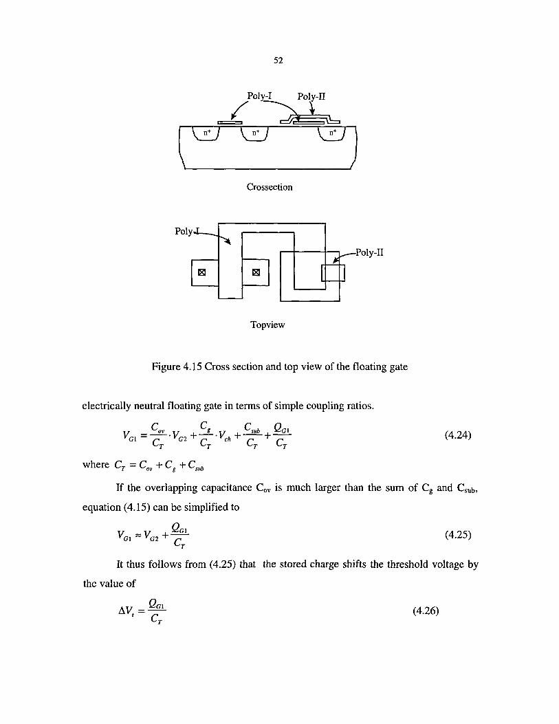
trimming circuits [CA89] [SG88]. Figure 4.15 shows a cross section and top view of a
parasitic floating gate transistor available in standard double poly CMOS processes. The
first polysilicon layer is used for the floating gate. The second polysilicon layer serves as
the control electrode and as the gate of all CMOS transistors used in the circuit. The write
operation is done during initial circuit testing. In the write operation, the floating gate is
charged with electrons tunneling along the edges of poly-I under poly-II, where tunneling
distance is reduced due to the thinning of the gate oxide associated with the step along the
edge of the Poly I layer. In the normal mode of operation, the floating gate can be
modeled by the circuit shown in Figure 4.16.
In this model Csub is the capacitance between the floating gate and the substrate,
COY is the overlapping capacitance between poly-I and poly-II, Cg is the capacitance
between the floating gate and the active region. The capacitance Cg is distributed and the
lower plate has a distributed voltage that represents the voltage along the channel. This
distributed channel voltage is often approximated to be the voltage at the source of the
transistor. QGI is stored charge on the floating gate. V G2 can be expressed for an
52
Poly--I Poly-II
1 ~i\S
Crossection
Poly-II
Topview
Figure 4.15 Cross section and top view of the floating gate
electrically neutral floating gate in terms of simple coupling ratios.
(4.24)
If the overlapping capacitance COy is much larger than the sum of Cg and Csub,
equation (4.15) can be simplified to
QGJ VG) "",VG2 +c
T
(4.25)
It thus follows from (4.25) that the stored charge shifts the threshold voltage by
the value of
llV = QGI t C
T
(4.26)
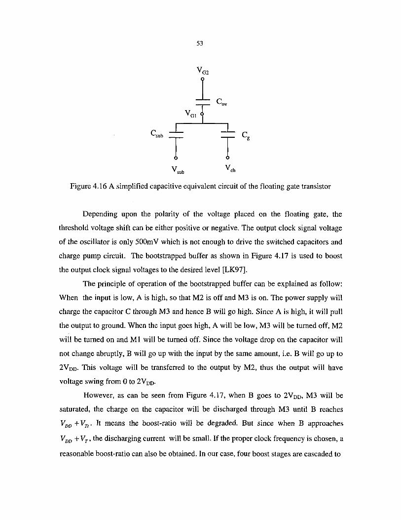
53
V02
1 COY
VOlT
Csub L l Cg
T T Vsub Vch
Figure 4.16 A simplified capacitive equivalent circuit of the floating gate transistor
Depending upon the polarity of the voltage placed on the floating gate, the
threshold voltage shift can be either positive or negative. The output clock signal voltage
of the oscillator is only 500m V which is not enough to drive the switched capacitors and
charge pump circuit. The bootstrapped buffer as shown in Figure 4.17 is used to boost
the output clock signal voltages to the desired level [LK97].
The principle of operation of the bootstrapped buffer can be explained as follow:
When the input is low, A is high, so that M2 is off and M3 is on. The power supply will
charge the capacitor C through M3 and hence B will go high. Since A is high, it will pull
the output to ground. When the input goes high, A will be low, M3 will be turned off, M2
will be turned on and MI will be turned off. Since the voltage drop on the capacitor will
not change abruptly, B will go up with the input by the same amount, i.e. B will go up to
2V DD. This voltage will be transferred to the output by M2, thus the output will have
voltage swing from 0 to 2VDD•
However, as can be seen from Figure 4.17, when B goes to 2VDD, M3 will be
saturated, the charge on the capacitor will be discharged through M3 until Breaches
VDD + VTt • It means the boost-ratio will be degraded. But since when B approaches
V DD + VT , the discharging current will be small. If the proper clock frequency is chosen, a
reasonable boost-ratio can also be obtained. In our case, four boost stages are cascaded to
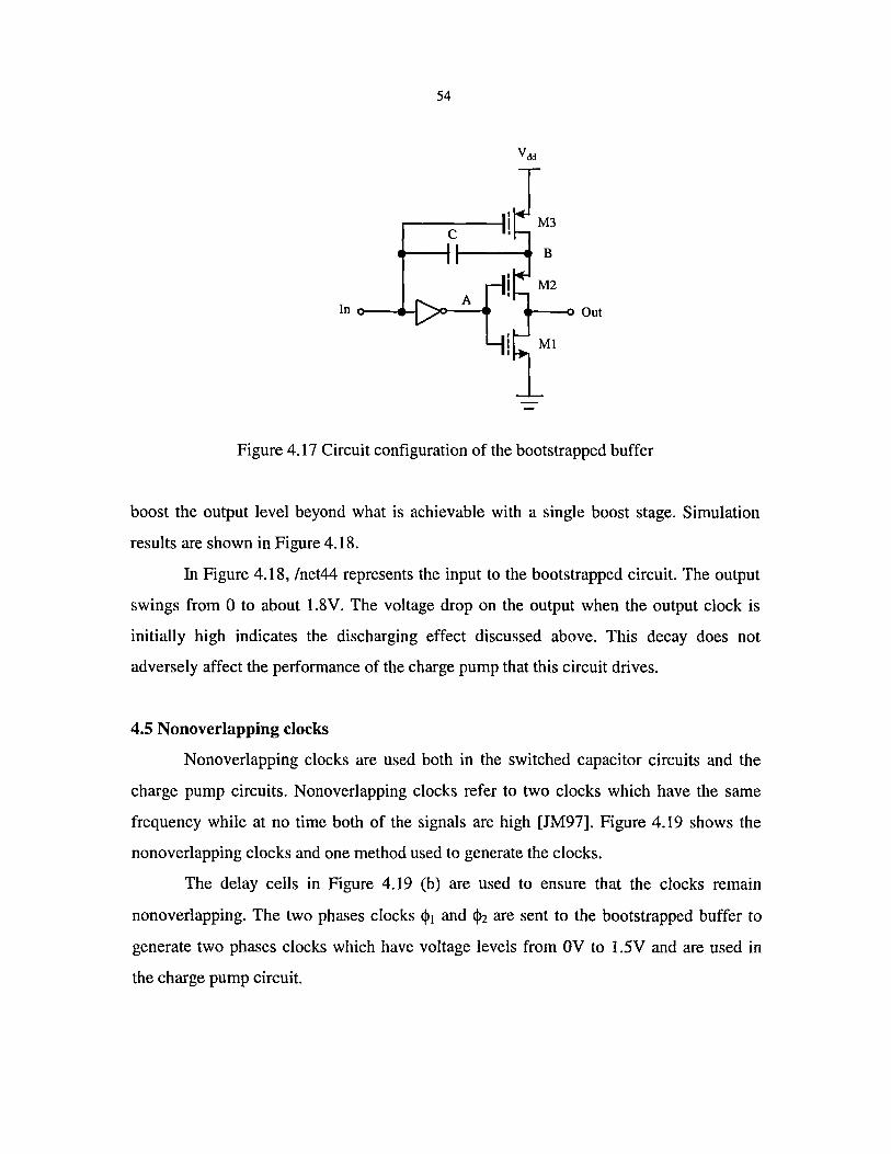
54
In o--~
M3
B
M2
'---0 Out
Ml
Figure 4.17 Circuit configuration of the bootstrapped buffer
boost the output level beyond what is achievable with a single boost stage. Simulation
results are shown in Figure 4.18.
In Figure 4.18, Inet44 represents the input to the bootstrapped circuit. The output
swings from 0 to about 1.8V. The voltage drop on the output when the output clock is
initially high indicates the discharging effect discussed above. This decay does not
adversely affect the performance of the charge pump that this circuit drives.
4.5 Nonoverlapping clocks
Nonoverlapping clocks are used both in the switched capacitor circuits and the
charge pump circuits. Nonoverlapping clocks refer to two clocks which have the same
frequency while at no time both of the signals are high [JM97]. Figure 4.19 shows the
nonoverlapping clocks and one method used to generate the clocks.
The delay cells in Figure 4.19 (b) are used to ensure that the clocks remain
nonoverlapping. The two phases clocks </>1 and <1>2 are sent to the bootstrapped buffer to
generate two phases clocks which have voltage levels from OV to 1.5V and are used in
the charge pump circuit.
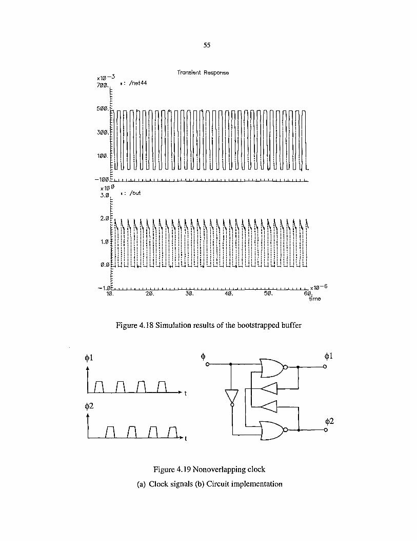
55
Transient Response
.: Inet44
I I I '" I I I I 1 "" I I I! 11", I lIt I I '" I I 1 I I "'" I! , 1 I
.: lout
~LL~'~'~'~'WI~'L'L'L'LILI~IJIJ'~'~'~'L'L'L'L'L'~'J'~I~'~' L'L'L'L'L'~'J'~'~'~' LILILILILI~I~I~I~x10-6 1121. 2121. 3121. 413. 50. 60.
time
Figure 4.18 Simulation results of the bootstrapped buffer
<\>1 <\>1
tn n n n • t
<\>2
t n n n n. t
<\>2
Figure 4.19 NonoverIapping clock
(a) Clock signals (b) Circuit implementation
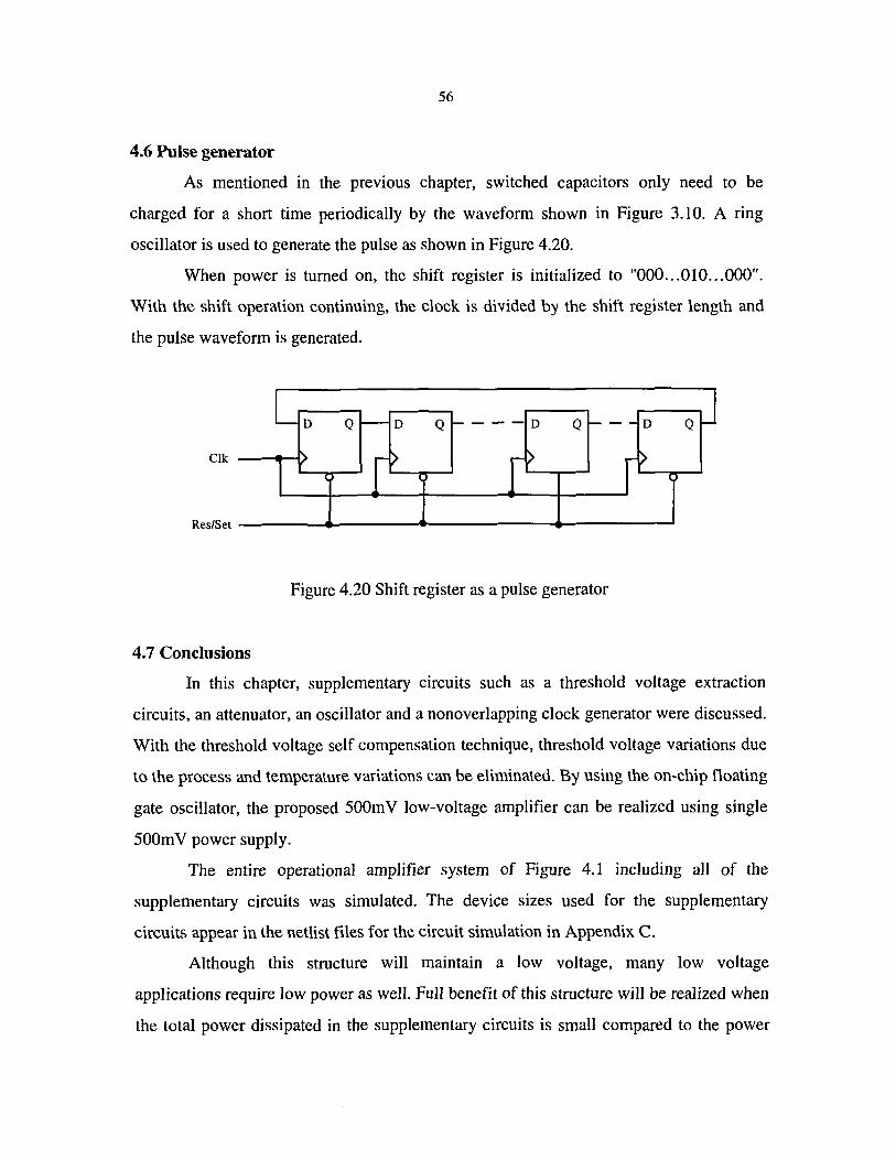
56
4.6 Pulse generator
As mentioned in the previous chapter, switched capacitors only need to be
charged for a short time periodically by the waveform shown in Figure 3.10. A ring
oscillator is used to generate the pulse as shown in Figure 4.20.
When power is turned on, the shift register is initialized to "000 ... 010 ... 000".
With the shift operation continuing, the clock is divided by the shift register length and
the pulse waveform is generated.
LD Q I-- D Q - --- D Q --- D QJ
elk 1 ~ ( [> r> >
Res/Set
Figure 4.20 Shift register as a pulse generator
4.7 Conclusions
In this chapter, supplementary circuits such as a threshold voltage extraction
circuits, an attenuator, an oscillator and a nonoverlapping clock generator were discussed.
With the threshold voltage self compensation technique, threshold voltage variations due
to the process and temperature variations can be eliminated. By using the on-chip floating
gate oscillator, the proposed 500m V low-voltage amplifier can be realized using single
500mV power supply.
The entire operational amplifier system of Figure 4.1 including all of the
supplementary circuits was simulated. The device sizes used for the supplementary
circuits appear in the netlist files for the circuit simulation in Appendix C.
Although this structure will maintain a low voltage, many low voltage
applications require low power as well. Full benefit of this structure will be realized when
the total power dissipated in the supplementary circuits is small compared to the power
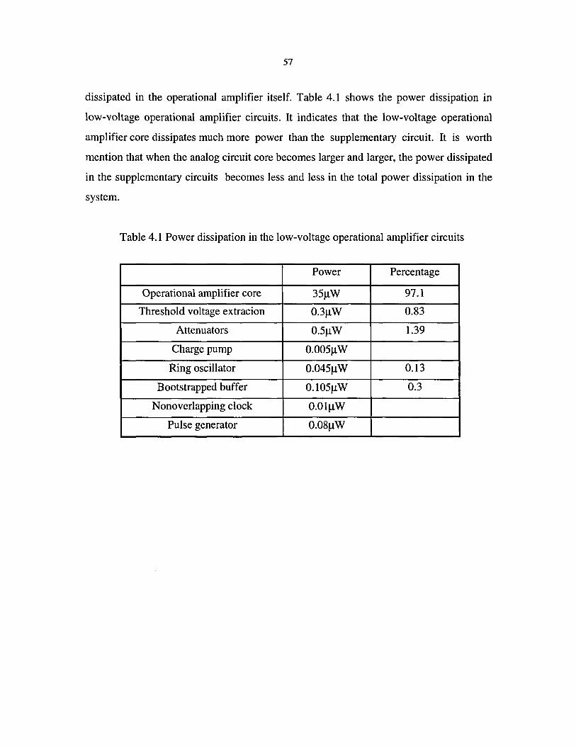
57
dissipated in the operational amplifier itself. Table 4.1 shows the power dissipation in
low-voltage operational amplifier circuits. It indicates that the low-voltage operational
amplifier core dissipates much more power than the supplementary circuit. It is worth
mention that when the analog circuit core becomes larger and larger, the power dissipated
in the supplementary circuits becomes less and less in the total power dissipation in the
system.
Table 4.1 Power dissipation in the low-voltage operational amplifier circuits
Power Percentage
Operational amplifier core 35JlW 97.1
Threshold voltage extracion 0.3JlW 0.S3
Attenuators 0.5JlW 1.39
Charge pump 0.005JlW
Ring oscillator 0.045JlW 0.13
Bootstrapped buffer 0.105JlW 0.3
Nonoverlapping clock O.OIJlW
Pulse generator O.OSJlW
58
CHAPTER 5. CONCLUSIONS
A new method for designing ultra-low-voltage integrated circuits in a standard
CMOS process was introduced. As a proof of concept vehicle, an ultra-low-voltage
operational amplifier was introduced.
Simulation results indicated that by lowering the effective threshold voltage, a
power supply voltage of 500m V for an operational amplifier can be used while still
maintaining comparable key performance parameters to the standard 3.3V operational
amplifier. The operational amplifier presented achieved a 68dB DC gain, 7.8MHz unit
gain bandwidth with a 65° phase margin compared to a 75dB DC gain, 10MHz unit-gain
bandwidth with a 60° phase margin for essentially the same amplifier designed to operate
with a standard 3.3V supply voltage.
To help place this work in perspective, there was considerable work on reducing
supply voltages to the 5V range in the mid-to-Iate 1980's. In the early 90's, linear circuits
that operated with 3.5V supplies started to appear with limited success with operation at
the 2V level. A small number of researchers have targeted the 1 V barrier with 100m V
power supply voltage reductions being viewed as substantial. These low-voltage circuits
often require very specialized processed. This work represents nearly a factor of 2
reduction in supply voltage down to the 500m V level while still using a standard
commercial CMOS process.
Although the focus in this thesis has been on maintaining performance parameters
comparable to those achievable with larger supply voltages and larger power dissipation,
it should be emphasized that the dominant applications of this technique will be for very
low-voltage systems. In these cases, substantial further decreases in power dissipation can
be attained paralleling a deterioration in amplifier bandwidth. This technique can also be
59
used for designing a variety of other analog and mixed-signal systems that operate at very
low-voltages and with low power levels.
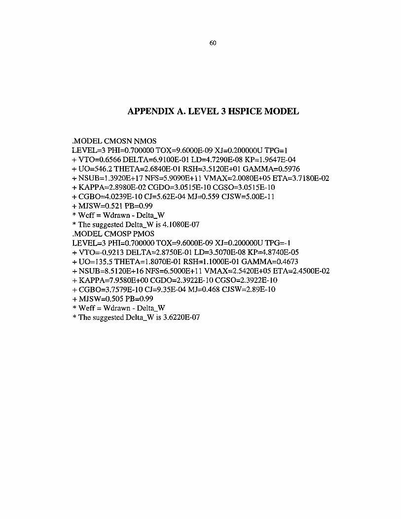
60
APPENDIX A. LEVEL 3 HSPICE MODEL
.MODEL CMOSN NMOS LEVEL=3 PHI=O.700000 TOX=9.6000E-09 XJ=O.200000U TPG=1 + VTO=O.6566 DELTA=6.9 lOOE-O 1 LD=4.7290E-08 KP=1.9647E-04 + UO=546.2 THETA=2.6840E-0l RSH=3.5120E+Ol GAMMA=O.5976 + NSUB= 1.3920E+ 17 NFS=5.9090E+ 11 VMAX=2.00S0E+05 ETA=3.71S0E-02 + KAPPA=2.89S0E-02 CGDO=3.0515E-1O CGSO=3.0515E-1O + CGBO=4.0239E-1O CJ=5.62E-04 MJ=O.559 CJSW=5.00E-ll + MJSW=O.521 PB=O.99 * Weff = Wdrawn - Delta_ W * The suggested Delta_ W is 4.1 OSOE-07 .MODEL CMOSP PMOS LEVEL:3 PHI=O.700000 TOX=9.6000E-09 XJ=O.200000U TPG=-1 + VTO=-O.9213 DELTA=2.S750E-Ol LD=3.5070E-08 KP=4.S740E-05 + UO=135.5 THETA=l.S070E-OI RSH=l.lOOOE-OI GAMMA=0.4673 + NSUB=8.5120E+ 16 NFS=6.5000E+ 11 VMAX=2.5420E+05 ET A=2.4500E-02 + KAPPA=7.9580E+OO CGDO=2.3922E-l 0 CGSO=2.3922E-l 0 + CGBO=3.7579E-1O CJ=9.35E-04 MJ=0.46S CJSW=2.S9E-1O + MJSW=0.505 PB=O.99 * Weff = W drawn - Delta_ W * The suggested Delta_ W is 3.6220E-07
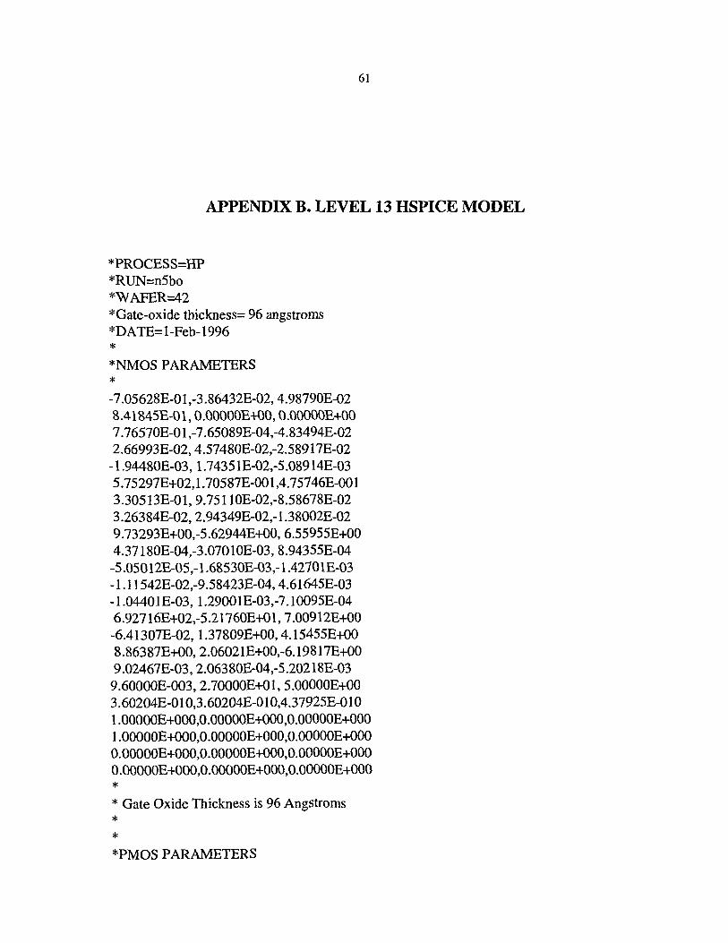
61
APPENDIX B. LEVEL 13 HSPICE MODEL
*PROCESS=HP *RUN=n5bo *WAFER=42 *Gate-oxide thickness= 96 angstroms *DATE= I-Feb-1996
* *NMOS PARAMETERS
* -7.05628E-Ol,-3.86432E-02,4.98790E-02 8.41845E-01, O.OooOOE+OO, O.OOOOOE+OO 7.76570E-Ol,-7.65089E-04,-4.83494E-02 2.66993E-02,4.57480E-02,-2.58917E-02
-1.94480E-03,1.74351E-02,-5.08914E-03 5.75297E+02,1.70587E-001,4.75746E-001 3.30513E-Ol,9.75110E-02,-8.58678E-02 3.26384E-02,2.94349E-02,-1.38oo2E-02 9.73293E+00,-5.62944E+00, 6.55955E+00 4.37180E-04,-3.07010E-03, 8.94355E-04 -5.050 12E-05,-1.68530E-03,-1.4270 lE-03 -1. 11542E-02,-9.58423E-04, 4.61645E-03 -1.04401E-03, 1.29001E-03,-7.1 0095E-04 6.92716E+02,-5.21760E+01,7.00912E+00
-6.41307E-02, 1.37809E+OO, 4. 15455E+00 8.86387E+00, 2.06021E+00,-6.19817E+00 9.02467E-03, 2.06380E-04,-5.20218E-03
9.60000E-003, 2.70000E+01, 5.00000E+00 3.60204E-OI0,3.60204E-OI0,4.37925E-OI0 1.00000E+000,0.00000E+000,0.00000E+000 1.00000E+000,0.00000E+000,0.00000E+OOO O.OOOOOE+OOO,O.OOOOOE+Ooo,O.ooOOOE+OOO O.OOOOOE+OOO,O.OOOOOE+OOO,O.OOOOOE+OOO
* * Gate Oxide Thickness is 96 Angstroms
* * *PMOS PARAMETERS
* -2.0261OE-Ol,3.59493E-02,-1.10651E-01 8.25364E-0 1, O.OOOOOE+OO, O.OOOOOE+OO 3.54162E-0 1 ,-6.88193E-02, 1.52476E-0 1
-4.51065E-02, 9.41324E-03, 3.52243E-02
62
-1.07507E-02, 1.96344E-02,-3.51067E-04 1.37992E+02,1.92169E-001,4.68470E-001 1.89331E-0 1, 6.30898E-02,-6.38388E-02 1.31710E-02, 1.44096E-02, 6.92372E-04 6.57709E+00,-1.56096E+00, 1.13564E+00 4.68478E-05,-1.09352E-03,-1.53111E-04 7.76679E-04,-1.97213E-04,-1.12034E-03 8.71439E-03,-1.92306E-03, 1.86243E-03 5.98941E-04, 4.54922E-04, 3. 11 794E-04 1.49460E+02, 1.36152E+01, 3.55246E+00 6.37235E+00,-6.63305E-Ol, 2.25929E+00
-1.21135E-02, 1.92973E+00, 1.00182E+00 -1. 16599E-03,-5.08278E-04, 9.56791E-04 9.60000E-003, 2.70000E+01, 5.00000E+00 4. 18427E-OI0,4. 18427E-OI0,4.33943E-OI0 1.00000E+000,0.00000E+000,0.00000E+000 1.00000E+000,0.00000E+000,0.00000E+000 O.OOOOOE+OOO,O.OOOOOE+OOO,O.OOOOOE+OOO O.OOOOOE+OOO,O.OOOOOE+OOO,O.OOOOOE+OOO
* *N+ diffusion::
* 2.1, 3.500000e-04, 2.900000e-10, le-08, 0.8 0.8, 0.44, 0.26, 0, 0
* *p+ diffusion::
* 2, 9.452900e-04, 2.458300e-1O, 1 e-08, 0.85 0.85, 0.439735, 0.237251, 0, 0
* *MET AL LAYER -- 1
* 0.07, 2.6e-05, 0, 0, 0 0, 0, 0, 0, 0
* *MET AL LAYER -- 2
* 0.07, 1.3e-05, 0, 0, 0 0, 0, 0, 0, 0
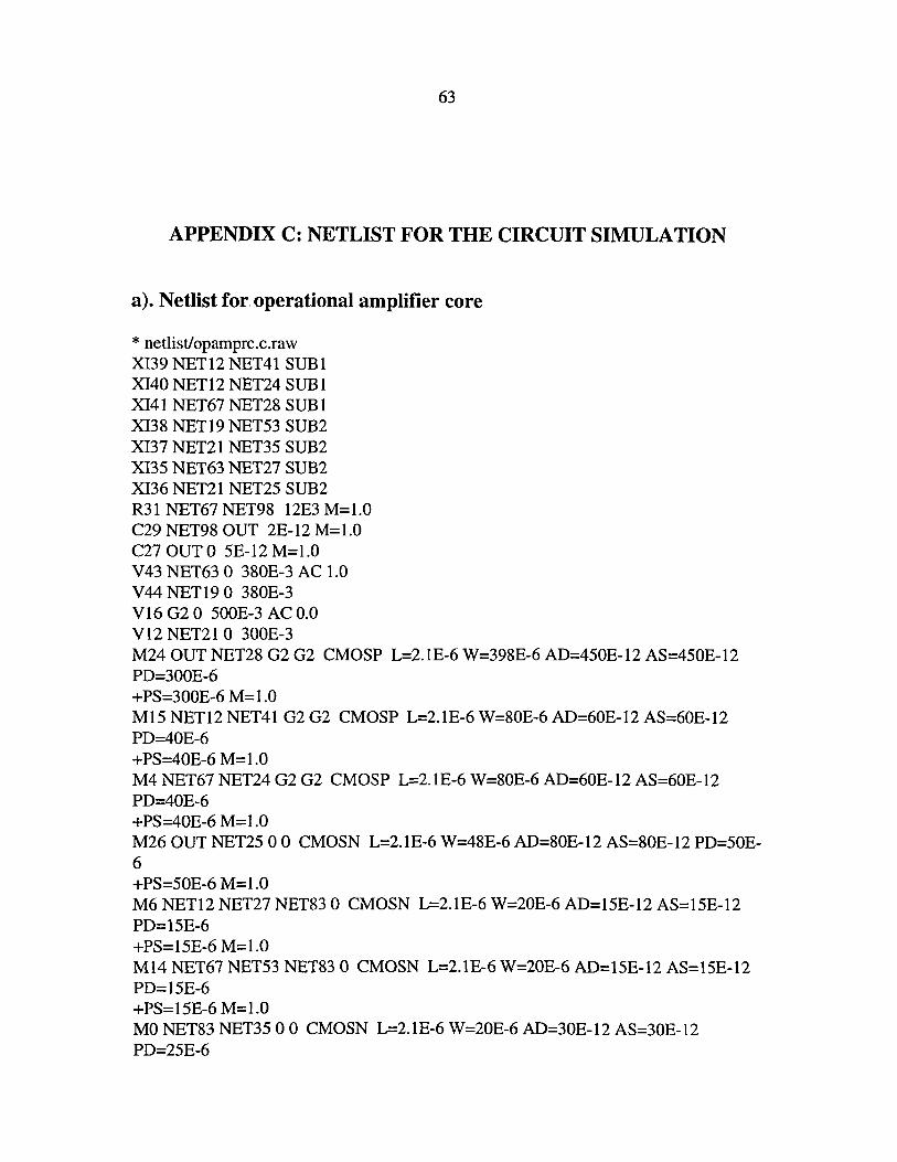
63
APPENDIX C: NETLIST FOR THE CIRCUIT SIMULATION
a). Netlist for, operational amplifier core
* netlist/opamprc.c.raw XI39 NET 12 NET41 SUB1 XI40 NET12 NET24 SUB 1 XI41 NET67 NET28 SUB 1 XI38 NET19 NET53 SUB2 XI37 NET21 NET35 SUB2 XI35 NET63 NET27 SUB2 XI36 NET21 NET25 SUB2 R31 NET67 NET98 12E3 M=l.O C29 NET98 OUT 2E-12 M=l.O C270UTO 5E-12 M=l.O V43 NET63 0 380E-3 AC 1.0 V44 NET19 0 380E-3 V16 G2 0 500E-3 AC 0.0 V12 NET21 0 300E-3 M24 OUT NET28 G2 G2 CMOSP L=2.1E-6 W=398E-6 AD=450E-12 AS=450E-12 PD=300E-6 +PS=300E-6 M= 1.0 M15 NET12 NET41 G2 G2 CMOSP L=2.1E-6 W=80E-6 AD=60E-12 AS=60E-12 PD=40E-6 +PS=40E-6 M=l.O M4 NET67 NET24 G2 G2 CMOSP L=2.1E-6 W=80E-6 AD=60E-12 AS=60E-12 PD=40E-6 +PS=40E-6 M=I.0 M26 OUT NET25 00 CMOSN L=2.1E-6 W=48E-6 AD=80E-12 AS=80E-12 PD=50E-6 +PS=50E-6 M=I.0 M6 NET12 NET27 NET83 0 CMOSN L=2.1E-6 W=20E-6 AD=15E-12 AS=15E-12 PD=15E-6 +PS=15E-6 M=1.0 M14 NET67 NET53 NET83 0 CMOSN L=2.1E-6 W=20E-6 AD=15E-12 AS=15E-12 PD=15E-6 +PS=15E-6 M=l.O MO NET83 NET35 0 0 CMOSN L=2.1E-6 W=20E-6 AD=30E-12 AS=30E-12 PD=25E-6
+PS=25E-6 M=I.O
.SUBCKT SUB I IN OUT VII NETl4 OUT 800E-3 RIO IN NET 14 100E9 M=1.0 Cl3 0 IN IE-I5 M=1.0 C70 OUT IE-I5 M=1.0 CO IN OUT lOE-12 M=1.0 .ENDS SUB I
.SUBCKT SUB2 IN OUT Vll OUT NET14 670E-3 RIO IN NETl4 lOE9 M=1.0 C13 0 IN IE-I5 M=1.0 C7 0 OUT IE-IS M=1.0 CO IN OUT 100E-12 M= 1.0 .ENDSSUB2
64
.AC DEC 10.0000 1.00000 1.000000E+ 10
.TEMP 25.0000
.OP
.save
.OPTION INGOLD=2 ARTIST=2 PSF=2 + PROBE=O + LIST + ACOUT = .OOOOOE+OO .END
65
b). Netlist for reference voltage generation circuits
* Threshold.c.raw .GLOBALGI XI17 NET 10 V3 SUB 1 XI16 Gl V4 SUB 1 XI15 0 VI SUB2 XI14 NET44 V2 SUB2 V8 010 3.3 M5 NETlO NETI0 Gl Gl CMOSP L=6E-6 W=24E-6 AD=36E-12 AS=36E-12 PD=50E-6 +PS=50E-6 M=I.0 M13 NETto Gl NET44 0 CMOSN L=180E-6 W=900E-9 AD=2E-12 AS=2E-12 PD=4.8E-6 +PS=4.8E-6 M=l.O MI NET44 NET44 0 0 CMOSN L=6E-6 W=6E-6 AD=9E-12 AS=9E-12 PD=15E-6 PS=15E-6 +M=1.0
.SUBCKT SUB 1 IN OUT M5 Gl IN OUT 0 CMOSN L=6E-6 W=6E-6 AD=9E-12 AS=O.O PD=15E-6 PS=15E-6 M=l.O MO OUT IN 0 0 CMOSN L=178E-6 W=900E-9 AD=2E-12 AS=2E-12 PD=4.8E-6 PS=4.8E-6 +M=I.O .ENDS SUBI
.SUBCKT SUB2 IN OUT Ml4 OUT IN 0101 CMOSP L=178E-6 W=900E-9 AD=2E-12 AS=2E-12 PD=4.8E-6 +PS=4.8E-6 M=1.0 Ml5 0 IN OUT Gl CMOSP L=6E-6 W=6E-6 AD=9E-12 AS=9E-12 PD=15E-6 PS=15E-6 +M=1.0 .ENDS SUB2
.TEMP 25.0000
.OP
.save
.OPTION INGOLD=2 ARTIST=2 PSF=2
66
+ PROBE=O + LIST + ACOUT = .OOOOOE+OO . END
67
c). Netlist for oscillator and bootstrapping circuits
* netlist/osc.c.raw .GLOBALGI V22 01 0 500E-3 R20 NET55 NET50 100E3 M=l.O ClOl NET198 NET153 lOE-12 M=1.0 C84 NET94 NET61 1 OE-12 M= 1.0 Cl18 NET114 NET65 lOE-12 M=l.O C83 NET106 NET133 lOE-12 M=1.0 C19 NET50 0 lOE-12 IC=l.O M=l.O M103 OUT NET161 00 CMOSN L=2E-6 W=lOE-6 AD=4.5E-12 AS=4.5E-12 PD=6E-6 +PS=6E-6 M=1.0 M37 NET153 NET161 00 CMOSN L=2E-6 W=lOE-6 AD=4.5E-12 AS=4.5E-12 PD=6E-6 +PS=6E-6 M=1.0 M94 NET 13 1 NET44 0 0 CMOSN L=2E-6 W=6E-6 AD=4.5E-12 AS=4.5E-12 PD=6E-6 +PS=6E-6 M=1.0 M99 NET161 NET131 00 CMOSN L=2E-6 W=18E-6 AD=4.5E-12 AS=4.5E-12 PD=6E-6 +PS=6E-6 M=1.0 M96 NET133 NET161 00 CMOSN L=2E-6 W=40E-6 AD=4.5E-12 AS=4.5E-12 PD=6E-6 +PS=6E-6 M=1.0 M97 NET61 NET161 00 CMOSN L=2E-6 W=lOE-6 AD=4.5E-12 AS=4.5E-12 PD=6E-6 +PS=6E-6 M=1.0 M36 NET65 NET161 00 CMOSN L=2E-6 W=lOE-6 AD=4.5E-12 AS=4.5E-12 PD=6E-6 +PS=6E-6 M=1.0 M124 NET44 NET40 0 0 CMOSN L=2E-6 W=3E-6 AD=4.5E-12 AS=4.5E-12 PD=6E-6 +PS=6E-6 M=1.0 M127 NET55 NET59 0 0 CMOSN L=2E-6 W=3E-6 AD=4.5E-12 AS=4.5E-12 PD=6E-6 +PS=6E-6 M=1.0 M125 NET 10 NET44 00 CMOSN L=2E-6 W=3E-6 AD=4.5E-12 AS=4.5E-12 PD=6E-6
68
+PS=6E-6 M= 1.0 M73 NET40 NETSO 0 0 CMOSN 1.=2E-6 W=3E-6 AD=4.5E-12 AS=4.5E-12 PD=6E-6 +PS=6E-6 M= 1.0 M126 NET59 NETlO 0 0 CMOSN L=2E-6 W=3E-6 AD=4.5E-12 AS=4.SE-12 PD=6E-6 +PS=6E-6 M= 1.0 M122 NET59 NETlO Gl G1 CMOSP L=2E-6 W=6E-6 AD=12E-12 AS=12E-12 PD=lOE-6 +PS=10E-6 M=l.O M12l NETlO NET44 Gl G1 CMOSP L=2E-6 W=6E-6 AD=12E-12 AS=12E-12 PD=10E-6 +PS=lOE-6 M=l.O MI20 NET44 NET40 GI Gl CMOSP L=2E-6 W=6E-6 AD=12E-12 AS=I2E-12 PD=lOE-6 +PS=10E-6 M=l.O MIll GI NETIS3 NETl98 NETl98 CMOSP L=2E-6 W=SE-6 AD=12E-12 AS=12E-12 +PD=10E-6 PS=10E-6 M=l.O M98 NET 13 I NET44 Gl Gl CMOSP L=2E-6 W=lSE-6 AD=12E-12 AS=12E-12 PD=lOE-6 +PS=lOE-6 M=l.O M69 NET40 NETSO GI Gl CMOSP L=2E-6 W=6E-6 AD=12E-12 AS=12E-12 PD=lOE-6 +PS=lOE-6 M=l.O MI05 OUTNET161 NETl98 NET198 CMOSP L=2E-6 W=30E-6 AD=4.SE-12 AS=4.5E-12 +PD=8E-6 PS::::8E-6 M= 1.0 M92 Gl NET133 NET 106 NET 106 CMOSP 1.=2E-6 W=3E-6 AD=12E-12 AS=12E-12 PD=lOE-6 +PS=lOE-6 M=l.O M34 NET65 NET161 NET94 NET94 CMOSP L=2E-6 W=30E-6 AD=4.5E-12 AS=4.5E-12 +PD=8E-6 PS=8E-6 M= 1.0 M35 NET153 NET161 NET114 NETl14 CMOSP L=2E-6 W=30E-6 AD=4.5E-12 AS=4.SE-12 +PD=8E-6 PS=8E-6 M=1.0 M91 NET133 NET161 GI GI CMOSP L=2E-6 W=60E-6 AD=12E-12 AS=12E-12 PD=10E-6 +PS=lOE-6 M=l.O M93 NET61 NETl61 NET 106 NET 106 CMOSP L=2E-6 W=30E-6 AD=4.SE-12 AS=4.5E-12 +PD=8E-6 PS=8E-6 M= 1.0 M109 G1 NET61 NET94 NET94 CMOSP L=2E-6 W=5E-6 AD=12E-12 AS=12E-12 PD=lOE-6
69
+PS=lOE-6 M=1.0 MIlO Gl NET65 NET114 NET114 CMOSP L=2E-6 W=5E-6 AD=12E-12 AS=12E-l2 PD=10E-6 +PS=lOE-6 M=1.0 Ml23 NET55 NET59 Gl Gl CMOSP L=2E-6 W=6E-6 AD=12E-12 AS=12E-12 PD=lOE-6 +PS=lOE-6 M=1.0 M85 NETl6l N;ET13 1 Gl Gl CMOSP L=2E-6 W=30E-6 AD=12E-12 AS=12E-12 PD=10E-6 +PS=lOE-6 M=1.0
.AC DEC 10.0000 1.00000 1.000000E+ 1 0
.TEMP 25.0000
.OP
.save
.OPTION INGOLD=2 ARTIST=2 PSF=2 + PROBE=O + LIST + ACOUT = .OOOOOE+OO .END
70
d). Netlist for the charge pump circuit
* cp.c.raw M13I NET220 PHI NET133 G1 CMOSP L=900E-9 W=6E-6 AD=9E-12 AS=9E-12 PD=I5E-6 +PS=15E-6 M=l.O M130 NET219 PHI NET125 Gl CMOSP L=900E-9 W=6E-6 AD=9E-12 AS=9E-12 PD=15E-6 +PS=15E-6 M=l.O M129 NET36 PHI NET157 G1 CMOSP L=900E-9 W=6E-6 AD=9E-12 AS=9E-12 PD=I5E-6 +PS=I5E-6 M=l.O M128 NET38 PHI NET7I G1 CMOSP L=900E-9 W=6E-6 AD=9E-12 AS=9E-12 PD=I5E-6 +PS=15E-6 M=l.O M127 NET42 PHI NET75 Gl CMOSP L=900E-9 W=6E-6 AD=9E-12 AS=9E-12 PD=I5E-6 +PS=15E-6 M=l.O M126 NET40 PHI NET9I Gl CMOSP L=900E-9 W=6E-6 AD=9E-12 AS=9E-12 PD=1 5E-6 +PS=15E-6 M=l.O M125 NET44 PHI NET87 GI CMOSP L=900E-9 W=6E-6 AD=9E-I2 AS=9E-12 PD=I5E-6 +PS=15E-6 M=l.O M124 NET46 PHI NET103 G1 CMOSP L=900E-9 W=6E-6 AD=9E-12 AS=9E-12 PD=15E-6 +PS=15E-6 M=l.O C106 NET2I9 NET157 lOOE-12 M=l.O ClIO NET220 NET125 lOOE-12 M=l.O C74 NET36 NET71 100E-12 M=l.O C35 OUT 0 1 OE-12 IC=O.O M= 1.0 C65 NET38 NET75 100E-12 M=l.O C64 NET42 NET9l lOOE-12 M=l.O C62 NET44 NETI03 100E-12 M=l.O C63 NET40 NET87 100E-12 M=l.O C7 NET46 0 100E-12 M=l.O MllI Gl PH2 NET220 0 CMOSN L=2E-6 W=3E-6 AD=4.5E-I2 AS=4.5E-12 PD=8E-6 +PS=8E-6 M=l.O
71
M107 G1 PH2 NET219 0 CMOSN L=2E-6 W=3E-6 AD=4.SE-12 AS=4.SE-12 PD=8E-6 +PS=8E-6 M=l.O MI08 NETl57 PH2 00 CMOSN L=2E-6 W=3E-6 AD=4.SE-12 AS=4.SE-12 PD=8E-6 +PS=8E-6 M=l.O Ml12 NET125 PH2 0 0 CMOSN L=2E-6 W=3E-6 AD=4.SE-12 AS=4.SE-12 PD=8E-6 +PS=8E-6 M= 1.0 Ml17 NET279 NET279 NET27S 0 CMOSN L=2E-6 W=3E-6 AD=4.5E-12 AS=4.SE-12 +PD=8E-6 PS=8E-6 M=l.O Ml18 NET27S NET27S NET287 0 CMOSN L=2E-6 W=3E-6 AD=4.5E-12 AS=4.SE-12 +PD=8E-6 PS=8E-6 M=l.O Ml19 NET287 NET287 00 CMOSN L=2E-6 W=3E-6 AD=4.5E-12 AS=4.SE-12 PD=8E-6 +PS=8E-6 M=l.O M120 OUT OUT NET279 0 CMOSN L=2E-6 W=3E-6 AD=4.5E-12 AS=4.SE-12 PD=8E-6 +PS=8E-6 M= 1.0 MS8 G 1 PH2 NET44 0 CMOSN L=2E-6 W=3E-6 AD=4.SE-12 AS=4.SE-12 PD=8E-6 PS=8E-6 +M=l.O MS9 GI PH2 NET40 0 CMOSN L=2E-6 W=3E-6 AD=4.SE-12 AS=4.SE-12 PD=8E-6 PS=8E-6 +M=l.O M71 G1 PH2 NET36 0 CMOSN L=2E-6 W=3E-6 AD=4.SE-12 AS=4.SE-12 PD=8E-6 PS=8E-6 +M=l.O M60 G1 PH2 NET42 0 CMOSN L=2E-6 W=3E-6 AD=4.SE-12 AS=4.SE-12 PD=8E-6 PS=8E-6 +M=l.O M30 NET133 NET133 OUT 0 CMOSN L=600E-9 W=3E-6 M=l.O M70 NET71 PH2 0 0 CMOSN L=2E-6 W=3E-6 AD=4.5E-12 AS=4.SE-12 PD=8E-6 PS=8E-6 +M=1.0 M69 NET75 PH2 00 CMOSN L=2E-6 W=3E-6 AD=4.SE-12 AS=4.5E-12 PD=8E-6 PS=8E-6 +M=l.O M67 NET87 PH2 00 CMOSN L=2E-6 W=3E-6 AD=4.SE-12 AS=4.SE-12 PD=8E-6 PS=8E-6 +M=l.O M68 NET91 PH2 0 0 CMOSN L=2E-6 W=3E-6 AD=4.SE-12 AS=4.SE-12 PD=8E-6 PS=8E-6 +M=l.O
72
M66 NET 103 PH20 0 CMOSN L=2E-6 W=3E-6 AD=4.SE-12 AS=4.SE-12 PD=8E-6 PS=8E-6 +M=l.O M61 Gl PH2 NET38 0 CMOSN L=2E-6 W=3E-6 AD=4.SE-12 AS=4.SE-12 PD=8E-6 PS=8E-6 +M=l.O M5 Gl PH2 NET46 0 CMOSN L=2E-6 W=3E-6 AD=4.5E-12 AS=4.SE-12 PD=8E-6 PS=8E-6 +M=l.O V2 G 1 0 500E-3 .AC DEC 10.0000 1.00000 1.000000E+ 10 .TEMP 2S.0000 .OP .save .OPTION INGOLD=2 ARTIST=2 PSF=2 + PROBE=O + LIST + ACOUT = .OOOOOE+OO . END
73
BIBLIOGRAPHY
[AB95] Phillip E. Allen, Benjamin J. Blalock and Gabriel A. Rincon, "A IV CMOS
Opamp' Using Bulk-Driven MOSFETs " , IEEE Int. Solid-State Circuits Conf.,
pp. 192-3, 1995.
[AC95] J. Ramirez-Angulo, S. C. Choi, and G. Gonzalez-Altamirano, "Low-Voltage
Circuits Building Blocks Using Multiple-Input Floating-Gate Transistors", IEEE
Transactions on Circuits and System-I: Fundamental Theory and Applications,
Vol. 42, No. 11, pp. 971-4, Nov. 1995.
[AH87] Phillip E. Allen and Douglas R. Holberg, CMOS Analog Circuit Design, Holt,
Rinehart and Winston, New York, 1987.
[CA89] L. Richard Carley, "Trimming Analog Circuits Using Floating-Gate Analog
MOS Memory", IEEE Int. Solid-State Circuits Conf., pp. 202-3, 1989.
[EC96] Jean-Paul Eggermont, Denis De Ceuster, et aI., "Design of SOl CMOS
Operational Amplifiers for Applications up to 300°C", IEEE J. Solid-State
Circuits, Vol. 31, No.2, pp. 179-86, Feb. 1996.
[FM89] Jeroen Fonderie, Marinus G. Maris and Johan H. Huijsing, "I-Volt Operation am
Amplifier with Rail-to-Rail Input and Output Ranges", IEEE Int. Solid-State
Circuits Conf., pp. 64-5, 1989.
[GA90] Randall L. Geiger, Phillip E. Allen and Neol R. Strader, VLSI Design
Techniques for Analog and Digital Circuits, McGraw-Hill, New York, 1990.
[HC97] Shu-Chuan Huang and Chin-Chun Chang, "Design of a BiCMOS Constant-gm
Rail-to-Rail Operational Amplifier for Low-Voltage Applications", IEEE IntI.
Symp. Circuits and Syst., Vol. 1, pp. 161-4, 1997.
[HH96] Ron Hogevorst and lohan H. Huijsing, Design of Low-Voltage, Low-Power
Operational Amplifier Cells, Kluwer Academic, The Netherlands, 1996.
74
[HL85] Johan H. Huijsing and Daniel Linebarger, "Low-Voltage Operational Amplifier
with Rail-to-Rail Input and Output Ranges", IEEE J. Solid-State Circuits, Vol.
SC-20, No.6, pp. 1144-49, Dec. 1985.
[JM97] David A. Johns and Ken Martin, Analog Integrated Circuit Design, John Wiley
and Sons, New York, 1997.
[KJ95] Joon-Yub Kim, Monolithic Finite Gain Amplifiers Employing Active Voltage
Attenuators in the Feedback and a Charge Conserving Macromodel for
MOSFETs, Ph.D dissertation, Iowa State University, 1995.
[KT96] Shigeru Kuhara, Hideo Toyoshima et al. "6nS 1.5V 4Mb BiCMOS SRAM",
Proc. IEEE Inter. Solid-State Circuits Conf., pp. 104-5, 1996.
[LK97] J. H. Lou and J. B. Kuo, "A 1.5-V Full-Swing Bootstrapped CMOS Large
Capacitive-Load Driver Circuit Suitable for Low-Voltage CMOS VLSI", IEEE
J. Solid-State Circuits, Vol. 32, No.1, pp. 119-21, Jan. 1997.
[MA96] Saqib Q. Malik, Design Methodology for Very Low Voltage CMOS Digital
Circuits, M.S thesis, Iowa State University, 1996.
[MU96] Igor Mucha, "Low-Voltage Current Operational Amplifier with A Very Low
Current Consumption", Proc. IEEE Inter. SYIVp. Cjrcuits and Syst., Vol. 1, - ...... ..-..- .... _¥ ..
pp525-28, 1996.
[RC95] J. Ramirez-Angulo, S. C. Choi and Gonzalez-Altamirano, "Low-Voltage
Circuits Building Blocks Using Multiple-Input Floating-Gate Transistors", IEEE
Transactions on Circuits and Systems I: Fundamental Theory and Application,
Vol. 42, No. 11, pp. 971-73) Nov, 1995.
[SG88] Eduard Sackinger and Walter Guggenbuhl, "An Analog Trimming Circuit Based
on a Floating-Gate Device", IEEE J. Solid-State Circuit, Vol. 23, No.6,
ppI437-40, Dec. 1988.
[SI95] Satoshi Sakurai and Mohammed Ismail, Low-voltage CMOS Operational
Amplifiers, Theory, Design and Implementation, Kluwer Academic, Boston,
1995.
75
[SI96] Satoshi Sakurai and Mohammed Ismail, "Robust Design of Rail-to-Rail CMOS
Operational Amplifiers for a Low Power Supply Voltage", IEEE J. of Solid
State and Circuits, Vol. 31, No.2, pp. 146-56, Feb. 1996.
[ST95] Shih-Wei Sun and Paul G. Y. Tsui, "Limitation of CMOS Supply-Voltage
Scaling by MOSFET Threshold-Voltage Variation", IEEE J. of Solid-Stage
Circuits, Vol. 30, No.8, pp. 947-49, Aug. 1995.
[WE93] Neil H. E. Weste and Kamran, Eshraghian, Principle of CMOS VLSI Design, a
System Perspective. Second Edition, Anderson-Wesley, New York, 1993.
[YU93] Chong-Gun Yu, A Digital Tuning Scheme for Digitally Programmable
Integrated Continuous-Time Filters and Techniques for High-Precision
Monolithic Linear Circuit Design and Implementation, Ph.D Dissertation, Iowa
State University, 1993.
Related Documents