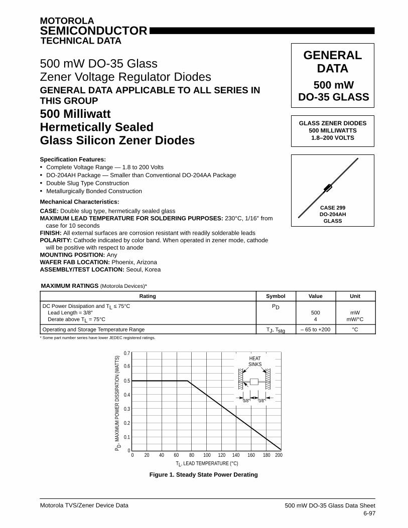
MOTOROLA SEMICONDUCTOR TECHNICAL DATA Motorola TVS/Zener Device Data 6-97 500 mW DO-35 Glass Data Sheet 500 mW DO-35 Glass Zener Voltage Regulator Diodes GENERAL DATA APPLICABLE TO ALL SERIES IN THIS GROUP 500 Milliwatt Hermetically Sealed Glass Silicon Zener Diodes Specification Features: • Complete Voltage Range — 1.8 to 200 Volts • DO-204AH Package — Smaller than Conventional DO-204AA Package • Double Slug Type Construction • Metallurgically Bonded Construction Mechanical Characteristics: CASE: Double slug type, hermetically sealed glass MAXIMUM LEAD TEMPERATURE FOR SOLDERING PURPOSES: 230°C, 1/16″ from case for 10 seconds FINISH: All external surfaces are corrosion resistant with readily solderable leads POLARITY: Cathode indicated by color band. When operated in zener mode, cathode will be positive with respect to anode MOUNTING POSITION: Any WAFER FAB LOCATION: Phoenix, Arizona ASSEMBLY/TEST LOCATION: Seoul, Korea MAXIMUM RATINGS (Motorola Devices)* Rating Symbol Value Unit DC Power Dissipation and T L ≤ 75°C Lead Length = 3/8″ Derate above T L = 75°C P D 500 4 mW mW/°C Operating and Storage Temperature Range T J , T stg – 65 to +200 °C * Some part number series have lower JEDEC registered ratings. 0.7 0.6 0.5 0.4 0.3 0.2 0.1 0 0 20 40 60 80 100 120 140 160 180 200 T L , LEAD TEMPERATURE (°C) P D , MAXIMUM POWER DISSIPATION (WATTS) Figure 1. Steady State Power Derating HEAT SINKS 3/8” 3/8” GENERAL DATA CASE 299 DO-204AH GLASS 500 mW DO-35 GLASS GLASS ZENER DIODES 500 MILLIWATTS 1.8–200 VOLTS

Welcome message from author
This document is posted to help you gain knowledge. Please leave a comment to let me know what you think about it! Share it to your friends and learn new things together.
Transcript
MOTOROLASEMICONDUCTORTECHNICAL DATA
Motorola TVS/Zener Device Data6-97
500 mW DO-35 Glass Data Sheet
500 mW DO-35 GlassZener Voltage Regulator DiodesGENERAL DATA APPLICABLE TO ALL SERIES INTHIS GROUP
500 MilliwattHermetically SealedGlass Silicon Zener DiodesSpecification Features:• Complete Voltage Range — 1.8 to 200 Volts• DO-204AH Package — Smaller than Conventional DO-204AA Package• Double Slug Type Construction• Metallurgically Bonded Construction
Mechanical Characteristics:
CASE: Double slug type, hermetically sealed glassMAXIMUM LEAD TEMPERATURE FOR SOLDERING PURPOSES: 230°C, 1/16″ from
case for 10 secondsFINISH: All external surfaces are corrosion resistant with readily solderable leadsPOLARITY: Cathode indicated by color band. When operated in zener mode, cathode
will be positive with respect to anodeMOUNTING POSITION: AnyWAFER FAB LOCATION: Phoenix, ArizonaASSEMBLY/TEST LOCATION: Seoul, Korea
MAXIMUM RATINGS (Motorola Devices)*
Rating Symbol Value Unit
DC Power Dissipation and TL ≤ 75°CLead Length = 3/8″Derate above TL = 75°C
PD5004
mWmW/°C
Operating and Storage Temperature Range TJ, Tstg – 65 to +200 °C* Some part number series have lower JEDEC registered ratings.
0.7
0.6
0.5
0.4
0.3
0.2
0.1
00 20 40 60 80 100 120 140 160 180 200
TL, LEAD TEMPERATURE (°C)
P D, M
AXIM
UM
PO
WER
DIS
SIPA
TIO
N (W
ATTS
)
Figure 1. Steady State Power Derating
HEATSINKS
3/8” 3/8”
GENERALDATA
CASE 299DO-204AH
GLASS
500 mWDO-35 GLASS
GLASS ZENER DIODES500 MILLIWATTS1.8–200 VOLTS

GENERAL DATA — 500 mW DO-35 GLASS
Motorola TVS/Zener Device Data6-98500 mW DO-35 Glass Data Sheet
APPLICATION NOTE — ZENER VOLTAGE
Since the actual voltage available from a given zener diodeis temperature dependent, it is necessary to determine junc-tion temperature under any set of operating conditions in orderto calculate its value. The following procedure is recom-mended:
Lead Temperature, TL, should be determined from:
TL = θLAPD + TA.
θLA is the lead-to-ambient thermal resistance (°C/W) and PD isthe power dissipation. The value for θLA will vary and dependson the device mounting method. θLA is generally 30 to 40°C/Wfor the various clips and tie points in common use and forprinted circuit board wiring.
The temperature of the lead can also be measured using athermocouple placed on the lead as close as possible to the tiepoint. The thermal mass connected to the tie point is normallylarge enough so that it will not significantly respond to heatsurges generated in the diode as a result of pulsed operationonce steady-state conditions are achieved. Using the mea-sured value of TL, the junction temperature may be deter-mined by:
TJ = TL + ∆TJL.
∆TJL is the increase in junction temperature above the leadtemperature and may be found from Figure 2 for dc power:
∆TJL = θJLPD.
For worst-case design, using expected limits of IZ, limits ofPD and the extremes of TJ(∆TJ) may be estimated. Changes involtage, VZ, can then be found from:
∆V = θVZTJ.
θVZ, the zener voltage temperature coefficient, is found fromFigures 4 and 5.
Under high power-pulse operation, the zener voltage willvary with time and may also be affected significantly by thezener resistance. For best regulation, keep current excursionsas low as possible.
Surge limitations are given in Figure 7. They are lower thanwould be expected by considering only junction temperature,as current crowding effects cause temperatures to be ex-tremely high in small spots, resulting in device degradationshould the limits of Figure 7 be exceeded.
L L
500
400
300
200
100
00 0.2 0.4 0.6 0.8 1
2.4–60 V
62–200 V
L, LEAD LENGTH TO HEAT SINK (INCH)JL, J
UN
CTI
ON
-TO
-LEA
D T
HER
MAL
RES
ISTA
NC
E (
C/W
)θ
°
Figure 2. Typical Thermal Resistance
TYPICAL LEAKAGE CURRENTAT 80% OF NOMINALBREAKDOWN VOLTAGE
+25°C
+125°C
100070005000
2000
1000700500
200
1007050
20
1075
2
10.70.5
0.2
0.10.070.05
0.02
0.010.0070.005
0.002
0.0013 4 5 6 7 8 9 10 11 12 13 14 15
VZ, NOMINAL ZENER VOLTAGE (VOLTS)
I, L
EAKA
GE
CU
RR
ENT
(A)µ
R
Figure 3. Typical Leakage Current
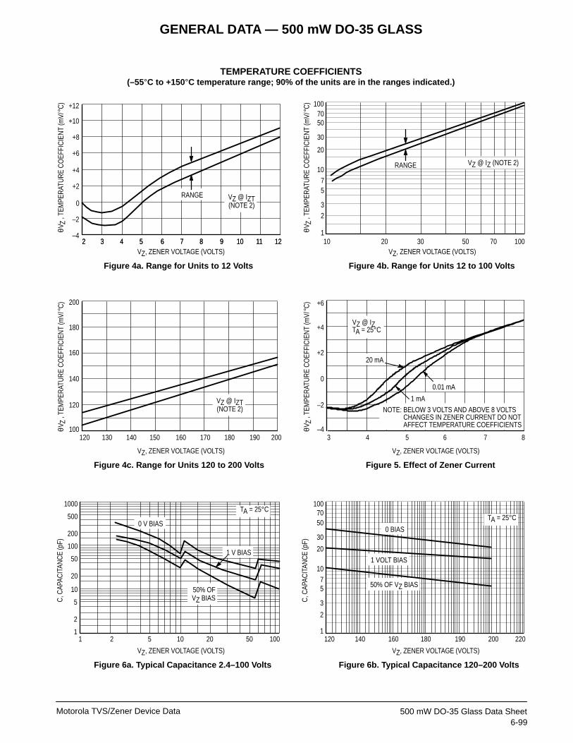
GENERAL DATA — 500 mW DO-35 GLASS
Motorola TVS/Zener Device Data6-99
500 mW DO-35 Glass Data Sheet
+12
+10
+8
+6
+4
+2
0
–2
–42 3 4 5 6 7 8 9 10 11 12
VZ, ZENER VOLTAGE (VOLTS)
Figure 4a. Range for Units to 12 Volts
VZ @ IZT(NOTE 2)
RANGE
TEMPERATURE COEFFICIENTS(–55°C to +150°C temperature range; 90% of the units are in the ranges indicated.)
1007050
30
20
10
75
3
2
12 3 4 5 6 7 8 9 10 11 12 10 20 30 50 70 100
VZ, ZENER VOLTAGE (VOLTS)
Figure 4b. Range for Units 12 to 100 Volts
RANGE VZ @ IZ (NOTE 2)
120 130 140 150 160 170 180 190 200
200
180
160
140
120
100
VZ, ZENER VOLTAGE (VOLTS)
Figure 4c. Range for Units 120 to 200 Volts
VZ @ IZT(NOTE 2)
+6
+4
+2
0
–2
–43 4 5 6 7 8
VZ, ZENER VOLTAGE (VOLTS)
Figure 5. Effect of Zener Current
NOTE: BELOW 3 VOLTS AND ABOVE 8 VOLTSNOTE: CHANGES IN ZENER CURRENT DO NOTNOTE: AFFECT TEMPERATURE COEFFICIENTS
1 mA
0.01 mA
VZ @ IZTA = 25°C
1000
C, C
APAC
ITAN
CE
(pF)
500
200
100
50
20
10
5
2
11 2 5 10 20 50 100
VZ, ZENER VOLTAGE (VOLTS)
Figure 6a. Typical Capacitance 2.4–100 Volts
TA = 25°C
0 V BIAS
1 V BIAS
50% OFVZ BIAS
1007050
30
20
1075
3
2
1120 140 160 180 190 200 220
VZ, ZENER VOLTAGE (VOLTS)
Figure 6b. Typical Capacitance 120–200 Volts
TA = 25°C
1 VOLT BIAS
50% OF VZ BIAS
0 BIAS
θVZ
, TEM
PER
ATU
RE
CO
EFFI
CIE
NT
(mV/
°C)
20 mA
C, C
APAC
ITAN
CE
(pF)
θVZ
, TEM
PER
ATU
RE
CO
EFFI
CIE
NT
(mV/
°C)
θVZ
, TEM
PER
ATU
RE
CO
EFFI
CIE
NT
(mV/
°C)
θVZ
, TEM
PER
ATU
RE
CO
EFFI
CIE
NT
(mV/
°C)
GENERAL DATA — 500 mW DO-35 GLASS
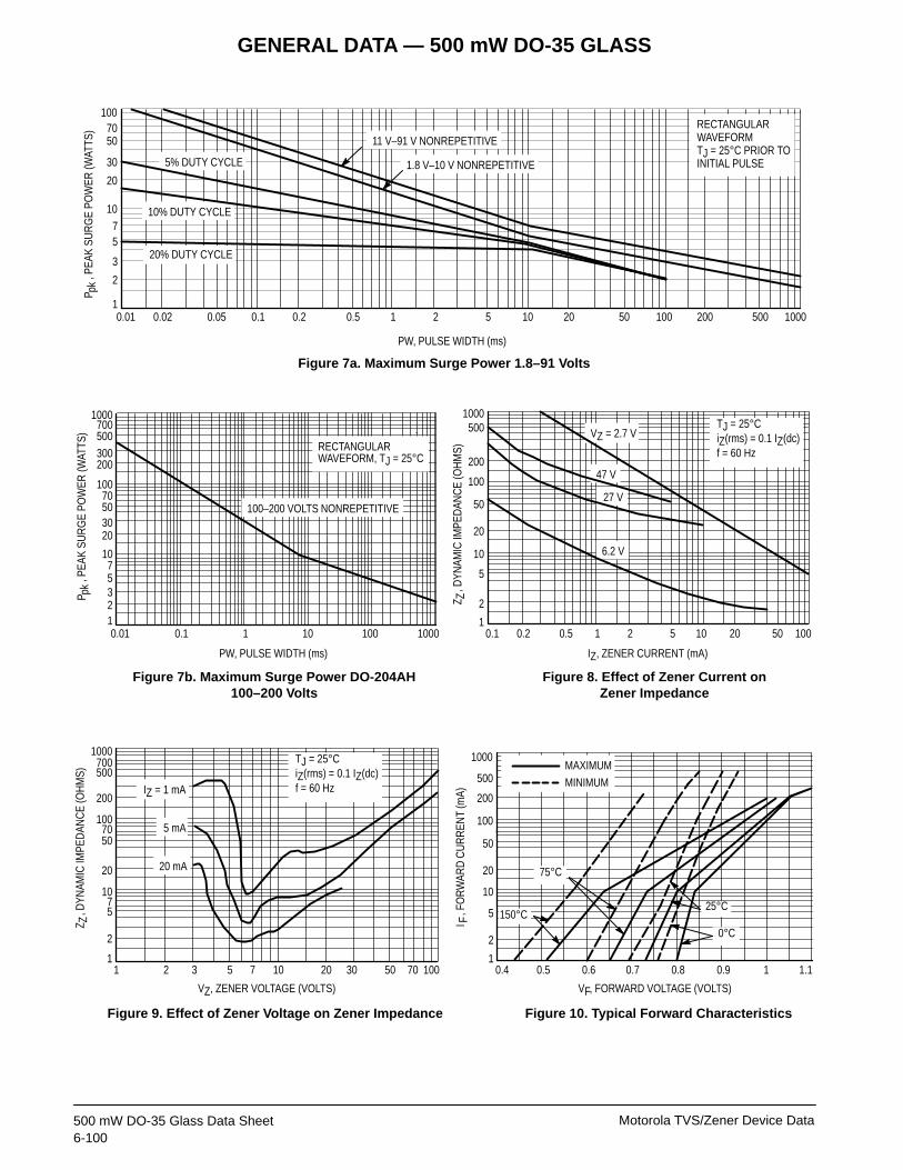
Motorola TVS/Zener Device Data6-100500 mW DO-35 Glass Data Sheet
1007050
30
20
1075
3
2
10.01 0.02 0.05 0.1 0.2 0.5 1 2 5 10 20 50 100 200 500 1000
P pk
, PEA
K SU
RG
E PO
WER
(WAT
TS)
PW, PULSE WIDTH (ms)
5% DUTY CYCLE
10% DUTY CYCLE
20% DUTY CYCLE
11 V–91 V NONREPETITIVE
1.8 V–10 V NONREPETITIVE
RECTANGULARWAVEFORMTJ = 25°C PRIOR TOINITIAL PULSE
Figure 7a. Maximum Surge Power 1.8–91 Volts
1000700500300200
10070503020
10753210.01 0.1 1 10 100 1000
P pk
, PEA
K SU
RG
E PO
WER
(WAT
TS)
PW, PULSE WIDTH (ms)
Figure 7b. Maximum Surge Power DO-204AH100–200 Volts
1000500
200
100
50
20
10
1
2
5
0.1 0.2 0.5 1 2 5 10 20 50 100
IZ, ZENER CURRENT (mA)
Figure 8. Effect of Zener Current onZener Impedance
Z Z, D
YNAM
IC IM
PED
ANC
E (O
HM
S)
Z Z, D
YNAM
IC IM
PED
ANC
E (O
HM
S)
1000700500
200
1007050
20
1075
2
11 2 3 5 7 10 20 30 50 70 100
VZ, ZENER VOLTAGE (VOLTS)
Figure 9. Effect of Zener Voltage on Zener Impedance Figure 10. Typical Forward Characteristics
RECTANGULARWAVEFORM, TJ = 25°C
100–200 VOLTS NONREPETITIVE
TJ = 25°CiZ(rms) = 0.1 IZ(dc)f = 60 HzIZ = 1 mA
5 mA
20 mA
TJ = 25°CiZ(rms) = 0.1 IZ(dc)f = 60 Hz
VZ = 2.7 V
47 V
27 V
6.2 V
VF, FORWARD VOLTAGE (VOLTS)
0.4 0.5 0.6 0.7 0.8 0.9 1 1.1
1000
500
200
100
50
20
10
5
2
1
I F, F
OR
WAR
D C
UR
REN
T (m
A)
MINIMUM
MAXIMUM
150°C
75°C
0°C
25°C

GENERAL DATA — 500 mW DO-35 GLASS
Motorola TVS/Zener Device Data6-101
500 mW DO-35 Glass Data Sheet
Figure 11. Zener Voltage versus Zener Current — V Z = 1 thru 16 Volts
VZ, ZENER VOLTAGE (VOLTS)
I Z, Z
ENER
CU
RR
ENT
(mA)
20
10
1
0.1
0.011 2 3 4 5 6 7 8 9 10 11 12 13 14 15 16
TA = 25°
Figure 12. Zener Voltage versus Zener Current — V Z = 15 thru 30 Volts
VZ, ZENER VOLTAGE (VOLTS)
15 16 17 18 19 20 21 22 23 24 25 26 27 28 29 30
10
1
0.1
0.01
TA = 25°
I Z, Z
ENER
CU
RR
ENT
(mA)
GENERAL DATA — 500 mW DO-35 GLASS
Motorola TVS/Zener Device Data6-102500 mW DO-35 Glass Data Sheet
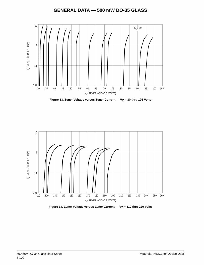
Figure 13. Zener Voltage versus Zener Current — V Z = 30 thru 105 Volts
VZ, ZENER VOLTAGE (VOLTS)
10
1
0.1
0.0130 35 40 45 50 55 60 70 75 80 85 90 95 100
Figure 14. Zener Voltage versus Zener Current — V Z = 110 thru 220 Volts
VZ, ZENER VOLTAGE (VOLTS)
110 120 130 140 150 160 170 180 190 200 210 220 230 240 250 260
10
1
0.1
0.01
TA = 25°
65 105
I Z, Z
ENER
CU
RR
ENT
(mA)
I Z, Z
ENER
CU
RR
ENT
(mA)
GENERAL DATA — 500 mW DO-35 GLASS
Motorola TVS/Zener Device Data6-103
500 mW DO-35 Glass Data Sheet
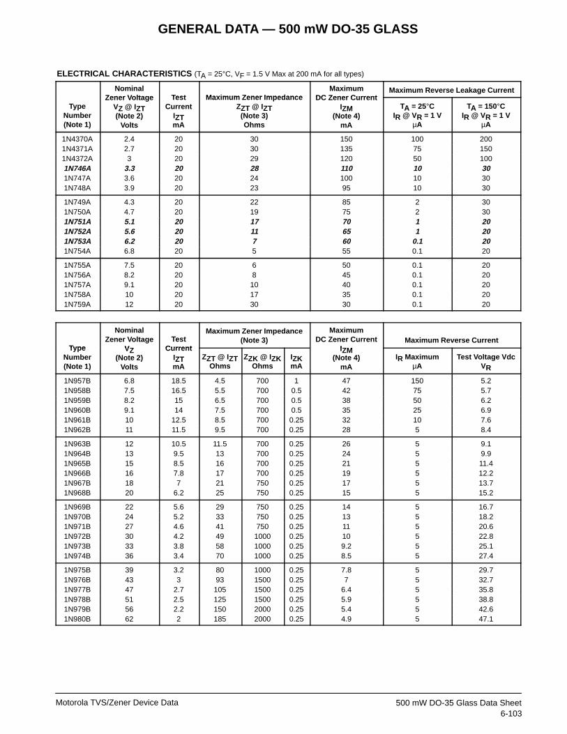
ELECTRICAL CHARACTERISTICS (TA = 25°C, VF = 1.5 V Max at 200 mA for all types)
T
NominalZener Voltage Test Maximum Zener Impedance
MaximumDC Zener Current
Maximum Reverse Leakage Current
TypeNumber(Note 1)
Zener VoltageVZ @ IZT(Note 2)
Volts
TestCurrent
IZTmA
Maximum Zener ImpedanceZZT @ IZT
(Note 3)Ohms
DC Zener Curren tIZM
(Note 4)mA
TA = 25°CIR @ VR = 1 V
µA
TA = 150°CIR @ VR = 1 V
µA
1N4370A 2.4 20 30 150 100 2001N4371A 2.7 20 30 135 75 1501N4372A 3 20 29 120 50 1001N746A 3.3 20 28 110 10 301N747A 3.6 20 24 100 10 301N748A 3.9 20 23 95 10 30
1N749A 4.3 20 22 85 2 301N750A 4.7 20 19 75 2 301N751A 5.1 20 17 70 1 201N752A 5.6 20 11 65 1 201N753A 6.2 20 7 60 0.1 201N754A 6.8 20 5 55 0.1 20
1N755A 7.5 20 6 50 0.1 201N756A 8.2 20 8 45 0.1 201N757A 9.1 20 10 40 0.1 201N758A 10 20 17 35 0.1 201N759A 12 20 30 30 0.1 20
Type
NominalZener Voltage
VZ
TestCurrent
Maximum Zener Impedance(Note 3)
MaximumDC Zener Current
IZMMaximum Reverse Current
TypeNumber(Note 1)
VZ(Note 2)
Volts
Curren tIZTmA
ZZT @ IZTOhms
ZZK @ IZKOhms
IZKmA
IZM(Note 4)
mAIR Maximum
µATest Voltage Vdc
VR
1N957B 6.8 18.5 4.5 700 1 47 150 5.21N958B 7.5 16.5 5.5 700 0.5 42 75 5.71N959B 8.2 15 6.5 700 0.5 38 50 6.21N960B 9.1 14 7.5 700 0.5 35 25 6.91N961B 10 12.5 8.5 700 0.25 32 10 7.61N962B 11 11.5 9.5 700 0.25 28 5 8.4
1N963B 12 10.5 11.5 700 0.25 26 5 9.11N964B 13 9.5 13 700 0.25 24 5 9.91N965B 15 8.5 16 700 0.25 21 5 11.41N966B 16 7.8 17 700 0.25 19 5 12.21N967B 18 7 21 750 0.25 17 5 13.71N968B 20 6.2 25 750 0.25 15 5 15.2
1N969B 22 5.6 29 750 0.25 14 5 16.71N970B 24 5.2 33 750 0.25 13 5 18.21N971B 27 4.6 41 750 0.25 11 5 20.61N972B 30 4.2 49 1000 0.25 10 5 22.81N973B 33 3.8 58 1000 0.25 9.2 5 25.11N974B 36 3.4 70 1000 0.25 8.5 5 27.4
1N975B 39 3.2 80 1000 0.25 7.8 5 29.71N976B 43 3 93 1500 0.25 7 5 32.71N977B 47 2.7 105 1500 0.25 6.4 5 35.81N978B 51 2.5 125 1500 0.25 5.9 5 38.81N979B 56 2.2 150 2000 0.25 5.4 5 42.61N980B 62 2 185 2000 0.25 4.9 5 47.1

GENERAL DATA — 500 mW DO-35 GLASS
Motorola TVS/Zener Device Data6-104500 mW DO-35 Glass Data Sheet
Type
NominalZener Voltage
VZ
TestCurrent
Maximum Zener Impedance(Note 3)
MaximumDC Zener Current
IZMMaximum Reverse Leakage Current
TypeNumber(Note 1)
VZ(Note 2)
Volts
Curren tIZTmA
ZZT @ IZTOhms
ZZK @ IZKOhms
IZKmA
IZM(Note 4)
mAIR Maximum
µATest Voltage Vdc
VR
1N981B 68 1.8 230 2000 0.25 4.5 5 51.71N982B 75 1.7 270 2000 0.25 4.1 5 561N983B 82 1.5 330 3000 0.25 3.7 5 62.21N984B 91 1.4 400 3000 0.25 3.3 5 69.21N985B 100 1.3 500 3000 0.25 3 5 761N986B 110 1.1 750 4000 0.25 2.7 5 83.6
1N987B 120 1 900 4500 0.25 2.5 5 91.21N988B 130 0.95 1100 5000 0.25 2.3 5 98.81N989B 150 0.85 1500 6000 0.25 2 5 1141N990B 160 0.8 1700 6500 0.25 1.9 5 121.61N991B 180 0.68 2200 7100 0.25 1.7 5 136.81N992B 200 0.65 2500 8000 0.25 1.5 5 152
NOTE 1. TOLERANCE AND VOLTAGE DESIGNATION
Tolerance DesignationThe type numbers shown have tolerance designations as follows:1N4370A series: ±5% units, C for ±2%, D for ±1%.1N746A series: ±5% units, C for ±2%, D for ±1%.1N957B series: ±5% units, C for ±2%, D for ±1%.
NOTE 2. ZENER VOLTAGE (VZ) MEASUREMENT
Nominal zener voltage is measured with the device junction in thermal equilibrium at the leadtemperature of 30°C ±1°C and 3/8″ lead length.
NOTE 3. ZENER IMPEDANCE (ZZ) DERIVATION
ZZT and ZZK are measured by dividing the ac voltage drop across the device by the ac currentapplied. The specified limits are for IZ(ac) = 0.1 IZ(dc) with the ac frequency = 60 Hz.
NOTE 4. MAXIMUM ZENER CURRENT RATINGS (IZM)
Values shown are based on the JEDEC rating of 400 mW. Where the actual zener voltage(VZ) is known at the operating point, the maximum zener current may be increased and islimited by the derating curve.

GENERAL DATA — 500 mW DO-35 GLASS
Motorola TVS/Zener Device Data6-105
500 mW DO-35 Glass Data Sheet
Low level oxide passivated zener diodes for applications re-quiring extremely low operating currents, low leakage, andsharp breakdown voltage.
• Zener Voltage Specified @ IZT = 50 µA• Maximum Delta VZ Given from 10 to 100 µA
ELECTRICAL CHARACTERISTICS (TA = 25°C, VF = 1.5 V Max at IF = 100 mA for all types)
TypeNumber
Zener VoltageVZ @ IZT = 50 µA
Volts
MaximumReverse Current
IR µA
TestVoltageVR Volts
MaximumZener Current
IZM mA
MaximumVoltage Change
∆VZ VoltsNumber(Note 1) Nom (Note 1) Min Max (Note 3)
IZM mA(Note 2)
∆VZ Volts(Note 4)
1N4678 1.8 1.71 1.89 7.5 1 120 0.71N4679 2 1.9 2.1 5 1 110 0.71N4680 2.2 2.09 2.31 4 1 100 0.751N4681 2.4 2.28 2.52 2 1 95 0.81N4682 2.7 2.565 2.835 1 1 90 0.85
1N4683 3 2.85 3.15 0.8 1 85 0.91N4684 3.3 3.135 3.465 7.5 1.5 80 0.951N4685 3.6 3.42 3.78 7.5 2 75 0.951N4686 3.9 3.705 4.095 5 2 70 0.971N4687 4.3 4.085 4.515 4 2 65 0.99
1N4688 4.7 4.465 4.935 10 3 60 0.991N4689 5.1 4.845 5.355 10 3 55 0.971N4690 5.6 5.32 5.88 10 4 50 0.961N4691 6.2 5.89 6.51 10 5 45 0.951N4692 6.8 6.46 7.14 10 5.1 35 0.9
1N4693 7.5 7.125 7.875 10 5.7 31.8 0.751N4694 8.2 7.79 8.61 1 6.2 29 0.51N4695 8.7 8.265 9.135 1 6.6 27.4 0.11N4696 9.1 8.645 9.555 1 6.9 26.2 0.081N4697 10 9.5 10.5 1 7.6 24.8 0.1
1N4698 11 10.45 11.55 0.05 8.4 21.6 0.111N4699 12 11.4 12.6 0.05 9.1 20.4 0.121N4700 13 12.35 13.65 0.05 9.8 19 0.131N4701 14 13.3 14.7 0.05 10.6 17.5 0.141N4702 15 14.25 15.75 0.05 11.4 16.3 0.15
1N4703 16 15.2 16.8 0.05 12.1 15.4 0.161N4704 17 16.15 17.85 0.05 12.9 14.5 0.171N4705 18 17.1 18.9 0.05 13.6 13.2 0.181N4706 19 18.05 19.95 0.05 14.4 12.5 0.191N4707 20 19 21 0.01 15.2 11.9 0.2
1N4708 22 20.9 23.1 0.01 16.7 10.8 0.221N4709 24 22.8 25.2 0.01 18.2 9.9 0.241N4710 25 23.75 26.25 0.01 19 9.5 0.251N4711 27 25.65 28.35 0.01 20.4 8.8 0.271N4712 28 26.6 29.4 0.01 21.2 8.5 0.28
1N4713 30 28.5 31.5 0.01 22.8 7.9 0.31N4714 33 31.35 34.65 0.01 25 7.2 0.331N4715 36 34.2 37.8 0.01 27.3 6.6 0.361N4716 39 37.05 40.95 0.01 29.6 6.1 0.391N4717 43 40.85 45.15 0.01 32.6 5.5 0.43
NOTE 1. TOLERANCE AND VOLTAGE DESIGNATION (V Z)
The type numbers shown have a standard tolerance of ±5% on the nominal Zener voltage,C for ±2%, D for ±1%.
NOTE 2. MAXIMUM ZENER CURRENT RATINGS (IZM)
Maximum Zener current ratings are based on maximum Zener voltage of the individual unitsand JEDEC 250 mW rating.
NOTE 3. REVERSE LEAKAGE CURRENT (I R)
Reverse leakage currents are guaranteed and measured at VR as shown on the table.
NOTE 4. MAXIMUM VOLTAGE CHANGE ( ∆VZ)
Voltage change is equal to the difference between VZ at 100 µA and VZ at 10 µA.
NOTE 5. ZENER VOLTAGE (VZ) MEASUREMENT
Nominal Zener voltage is measured with the device junction in thermal equilibrium at the leadtemperature at 30°C ±1°C and 3/8″ lead length.

GENERAL DATA — 500 mW DO-35 GLASS
Motorola TVS/Zener Device Data6-106500 mW DO-35 Glass Data Sheet
ELECTRICAL CHARACTERISTICS (TA = 25°C unless otherwise noted. Based on dc measurements at thermal equilibrium; lead length= 3/8″; thermal resistance of heat sink = 30°C/W) VF = 1.1 Max @ IF = 200 mA for all types.
JEDEC
NominalZener Voltage
VZ @ IZT
TestCurrent
Max Zener Impedance(Note 4)
Max ReverseLeakage Current Max Zener Voltage
Temperature CoeffJEDECType No.(Note 1)
VZ @ IZTVolts
(Note 3)
Curren tIZTmA
ZZT @ IZTOhms
ZZK @ IZK = 0.25 mAOhms
IRµA
VRVolts
Tempera ture Coeff .θVZ (%/°C)
(Note 2)
1N5221B 2.4 20 30 1200 100 1 –0.0851N5222B 2.5 20 30 1250 100 1 –0.0851N5223B 2.7 20 30 1300 75 1 –0.081N5224B 2.8 20 30 1400 75 1 –0.081N5225B 3 20 29 1600 50 1 –0.075
1N5226B 3.3 20 28 1600 25 1 –0.071N5227B 3.6 20 24 1700 15 1 –0.0651N5228B 3.9 20 23 1900 10 1 –0.061N5229B 4.3 20 22 2000 5 1 ±0.0551N5230B 4.7 20 19 1900 5 2 ±0.03
1N5231B 5.1 20 17 1600 5 2 ±0.031N5232B 5.6 20 11 1600 5 3 +0.0381N5233B 6 20 7 1600 5 3.5 +0.0381N5234B 6.2 20 7 1000 5 4 +0.0451N5235B 6.8 20 5 750 3 5 +0.05
1N5236B 7.5 20 6 500 3 6 +0.0581N5237B 8.2 20 8 500 3 6.5 +0.0621N5238B 8.7 20 8 600 3 6.5 +0.0651N5239B 9.1 20 10 600 3 7 +0.0681N5240B 10 20 17 600 3 8 +0.075
1N5241B 11 20 22 600 2 8.4 +0.0761N5242B 12 20 30 600 1 9.1 +0.0771N5243B 13 9.5 13 600 0.5 9.9 +0.0791N5244B 14 9 15 600 0.1 10 +0.0821N5245B 15 8.5 16 600 0.1 11 +0.082
1N5246B 16 7.8 17 600 0.1 12 +0.0831N5247B 17 7.4 19 600 0.1 13 +0.0841N5248B 18 7 21 600 0.1 14 +0.0851N5249B 19 6.6 23 600 0.1 14 +0.0861N5250B 20 6.2 25 600 0.1 15 +0.086
1N5251B 22 5.6 29 600 0.1 17 +0.0871N5252B 24 5.2 33 600 0.1 18 +0.0881N5253B 25 5 35 600 0.1 19 +0.0891N5254B 27 4.6 41 600 0.1 21 +0.091N5255B 28 4.5 44 600 0.1 21 +0.091
1N5256B 30 4.2 49 600 0.1 23 +0.0911N5257B 33 3.8 58 700 0.1 25 +0.0921N5258B 36 3.4 70 700 0.1 27 +0.0931N5259B 39 3.2 80 800 0.1 30 +0.0941N5260B 43 3 93 900 0.1 33 +0.095
1N5261B 47 2.7 105 1000 0.1 36 +0.0951N5262B 51 2.5 125 1100 0.1 39 +0.0961N5263B 56 2.2 150 1300 0.1 43 +0.0961N5264B 60 2.1 170 1400 0.1 46 +0.0971N5265B 62 2 185 1400 0.1 47 +0.097
(continued)

GENERAL DATA — 500 mW DO-35 GLASS
Motorola TVS/Zener Device Data6-107
500 mW DO-35 Glass Data Sheet
ELECTRICAL CHARACTERISTICS — continued (TA = 25°C unless otherwise noted. Based on dc measurements at thermal equi-librium; lead length = 3/8″; thermal resistance of heat sink = 30°C/W) VF = 1.1 Max @ IF = 200 mA for all types.
JEDEC
NominalZener Voltage
VZ @ IZT
TestCurrent
Max Zener Impedance(Note 4)
Max ReverseLeakage Current Max Zener Voltage
Temperature CoeffJEDECType No.(Note 1)
VZ @ IZTVolts
(Note 3)
Curren tIZTmA
ZZT @ IZTOhms
ZZK @ IZK = 0.25 mAOhms
IRµA
VRVolts
Tempera ture Coeff .θVZ (%/°C)
(Note 2)
1N5266B 68 1.8 230 1600 0.1 52 +0.0971N5267B 75 1.7 270 1700 0.1 56 +0.0981N5268B 82 1.5 330 2000 0.1 62 +0.0981N5269B 87 1.4 370 2200 0.1 68 +0.0991N5270B 91 1.4 400 2300 0.1 69 +0.099
1N5271B 100 1.3 500 2600 0.1 76 +0.111N5272B 110 1.1 750 3000 0.1 84 +0.111N5273B 120 1 900 4000 0.1 91 +0.111N5274B 130 0.95 1100 4500 0.1 99 +0.111N5275B 140 0.9 1300 4500 0.1 106 +0.11
1N5276B 150 0.85 1500 5000 0.1 114 +0.111N5277B 160 0.8 1700 5500 0.1 122 +0.111N5278B 170 0.74 1900 5500 0.1 129 +0.111N5279B 180 0.68 2200 6000 0.1 137 +0.111N5280B 190 0.66 2400 6500 0.1 144 +0.111N5281B 200 0.65 2500 7000 0.1 152 +0.11
NOTE 1. TOLERANCE
The JEDEC type numbers shown indicate a tolerance of ±5%. For tighter tolerance devicesuse suffixes “C” for ±2% and “D” for ±1%.
NOTE 2. TEMPERATURE COEFFICIENT (θVZ)
Test conditions for temperature coefficient are as follows:a. IZT = 7.5 mA, T1 = 25°C,a. T2 = 125°C (1N5221B through 1N5242B).b. IZT = Rated IZT, T1 = 25°C,a. T2 = 125°C (1N5243B through 1N5281B).
Device to be temperature stabilized with current applied prior to reading breakdown voltageat the specified ambient temperature.
NOTE 3. ZENER VOLTAGE (VZ) MEASUREMENT
Nominal zener voltage is measured with the device junction in thermal equilibrium at the leadtemperature of 30°C ±1°C and 3/8″ lead length.
NOTE 4. ZENER IMPEDANCE (ZZ) DERIVATION
ZZT and ZZK are measured by dividing the ac voltage drop across the device by the ac currentapplied. The specified limits are for IZ(ac) = 0.1 IZ(dc) with the ac frequency = 60 Hz.
For more information on special selections contact your nearest Motorola representa-tive.
GENERAL DATA — 500 mW DO-35 GLASS
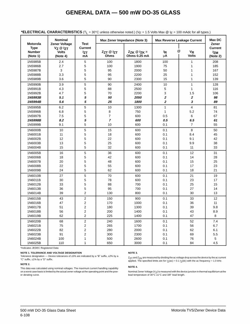
Motorola TVS/Zener Device Data6-108500 mW DO-35 Glass Data Sheet
*ELECTRICAL CHARACTERISTICS (TL = 30°C unless otherwise noted.) (VF = 1.5 Volts Max @ IF = 100 mAdc for all types.)
MotorolaNominal
Zener Voltage TestMax Zener Impedance (Note 3) Max Reverse Leakage Current Max DC
ZenerMotorolaType
Number(Note 1)
Zener VoltageVZ @ IZT
Volts(Note 4)
TestCurrent
IZTmA
ZZT @ IZTOhms
ZZK @ IZK =Ohms 0.25 mA
IRµA
VRVolts
ZenerCurrent
IZM(Note 2)
1N5985B 2.4 5 100 1800 100 1 2081N5986B 2.7 5 100 1900 75 1 1851N5987B 3 5 95 2000 50 1 1671N5988B 3.3 5 95 2200 25 1 1521N5989B 3.6 5 90 2300 15 1 139
1N5990B 3.9 5 90 2400 10 1 1281N5991B 4.3 5 88 2500 5 1 1161N5992B 4.7 5 70 2200 3 1.5 1061N5993B 5.1 5 50 2050 2 2 981N5994B 5.6 5 25 1800 2 3 89
1N5995B 6.2 5 10 1300 1 4 811N5996B 6.8 5 8 750 1 5.2 741N5997B 7.5 5 7 600 0.5 6 671N5998B 8.2 5 7 600 0.5 6.5 611N5999B 9.1 5 10 600 0.1 7 55
1N6000B 10 5 15 600 0.1 8 501N6001B 11 5 18 600 0.1 8.4 451N6002B 12 5 22 600 0.1 9.1 421N6003B 13 5 25 600 0.1 9.9 381N6004B 15 5 32 600 0.1 11 33
1N6005B 16 5 36 600 0.1 12 311N6006B 18 5 42 600 0.1 14 281N6007B 20 5 48 600 0.1 15 251N6008B 22 5 55 600 0.1 17 231N6009B 24 5 62 600 0.1 18 21
1N6010B 27 5 70 600 0.1 21 191N6011B 30 5 78 600 0.1 23 171N6012B 33 5 88 700 0.1 25 151N6013B 36 5 95 700 0.1 27 141N6014B 39 2 130 800 0.1 30 13
1N6015B 43 2 150 900 0.1 33 121N6016B 47 2 170 1000 0.1 36 111N6017B 51 2 180 1300 0.1 39 9.81N6018B 56 2 200 1400 0.1 43 8.91N6019B 62 2 225 1400 0.1 47 8
1N6020B 68 2 240 1600 0.1 52 7.41N6021B 75 2 265 1700 0.1 56 6.71N6022B 82 2 280 2000 0.1 62 6.11N6023B 91 2 300 2300 0.1 69 5.51N6024B 100 1 500 2600 0.1 76 51N6025B 110 1 650 3000 0.1 84 4.5
*Indicates JEDEC Registered Data
NOTE 1. TOLERANCE AND VOLTAGE DESIGNATIONTolerance designation — Device tolerances of ±5% are indicated by a “B” suffix, ±2% by a“C” suffix, ±1% by a “D” suffix.
NOTE 2.
This data was calculated using nominal voltages. The maximum current handling capabilityon a worst case basis is limited by the actual zener voltage at the operating point and the pow-er derating curve.
NOTE 3.
ZZT and ZZK are measured by dividing the ac voltage drop across the device by the ac currentapplied. The specified limits are for IZ(ac) = 0.1 IZ(dc) with the ac frequency = 1.0 kHz.
NOTE 4.
Nominal Zener Voltage (VZ) is measured with the device junction in thermal equilibrium at thelead temperature of 30°C ±1°C and 3/8″ lead length.
@

GENERAL DATA — 500 mW DO-35 GLASS
Motorola TVS/Zener Device Data6-109
500 mW DO-35 Glass Data Sheet
ELECTRICAL CHARACTERISTICS (TL = 30°C unless otherwise noted.) (VF = 1.3 Volts Max, IF = 100 mAdc for all types.)
VZT at IZT(V)
Max ZenerImpedance
(Note 3)
I
Max ReverseLeakage Current
IR at VR(µA)
IMotorolaType
NumberMin
(Note 1)Max
(Note 1)
(Note 3)ZZT @ IZT
(Ohms)Max
IZT(mA)
Tamb25°CMax
Tamb125°CMax
VR(V)
IZM(mA)
(Note 2)
BZX55C2V4RL 2.28 2.56 85 5 50 100 1 155BZX55C2V7RL 2.5 2.9 85 5 10 50 1 135BZX55C3V0RL 2.8 3.2 85 5 4 40 1 125BZX55C3V3RL 3.1 3.5 85 5 2 40 1 115BZX55C3V6RL 3.4 3.8 85 5 2 40 1 105
BZX55C3V9RL 3.7 4.1 85 5 2 40 1 95BZX55C4V3RL 4 4.6 75 5 1 20 1 90BZX55C4V7RL 4.4 5 60 5 0.5 10 1 85BZX55C5V1RL 4.8 5.4 35 5 0.1 2 1 80BZX55C5V6RL 5.2 6 25 5 0.1 2 1 70
BZX55C6V2RL 5.8 6.6 10 5 0.1 2 2 64BZX55C6V8RL 6.4 7.2 8 5 0.1 2 3 58BZX55C7V5RL 7 7.9 7 5 0.1 2 5 53BZX55C8V2RL 7.7 8.7 7 5 0.1 2 6 47BZX55C9V1RL 8.5 9.6 10 5 0.1 2 7 43
BZX55C10RL 9.4 10.6 15 5 0.1 2 7.5 40BZX55C11RL 10.4 11.6 20 5 0.1 2 8.5 36BZX55C12RL 11.4 12.7 20 5 0.1 2 9 32BZX55C13RL 12.4 14.1 26 5 0.1 2 10 29BZX55C15RL 13.8 15.6 30 5 0.1 2 11 27
BZX55C16RL 15.3 17.1 40 5 0.1 2 12 24BZX55C18RL 16.8 19.1 50 5 0.1 2 14 21BZX55C20RL 18.8 21.1 55 5 0.1 2 15 20BZX55C22RL 20.8 23.3 55 5 0.1 2 17 18BZX55C24RL 22.8 25.6 80 5 0.1 2 18 16
BZX55C27RL 25.1 28.9 80 5 0.1 2 20 14BZX55C30RL 28 32 80 5 0.1 2 22 13BZX55C33RL 31 35 80 5 0.1 2 24 12BZX55C36RL 34 38 80 5 0.1 2 27 11BZX55C39RL 37 41 90 2.5 0.1 5 28 10
BZX55C43RL 40 46 90 2.5 0.1 5 32 9.2BZX55C47RL 44 50 110 2.5 0.1 5 35 8.5BZX55C51RL 48 54 125 2.5 0.1 10 38 7.8BZX55C56RL 52 60 135 2.5 0.1 10 42 7BZX55C62RL 58 66 150 2.5 0.1 10 47 6.4
BZX55C68RL 64 72 160 2.5 0.1 10 51 5.9BZX55C75RL 70 80 170 2.5 0.1 10 56 5.3BZX55C82RL 77 87 200 2.5 0.1 10 62 4.8BZX55C91RL 85 96 250 1 0.1 10 69 4.3
NOTE 1. TOLERANCE AND VOLTAGE DESIGNATION
Tolerance designation — The type numbers listed have zener voltage min/max limits asshown. Device tolerance of ±2% are indicated by a “B” instead of a “C”. Zener voltage is mea-sured with the device junction in thermal equilibrium at the lead temperature of 30°C ±1°Cand 3/8″ lead length.
NOTE 2.
This data was calculated using nominal voltages. The maximum current handling capability
on a worst case basis is limited by the actual zener voltage at the operating point and the pow-er derating curve.
NOTE 3.
ZZT and ZZK are measured by dividing the ac voltage drop across the device by the ac currentapplied. The specified limtis are for IZ(ac) = 0.1 IZ(dc) with the ac frequency = 1.0 kHz.
GENERAL DATA — 500 mW DO-35 GLASS
Motorola TVS/Zener Device Data6-110500 mW DO-35 Glass Data Sheet
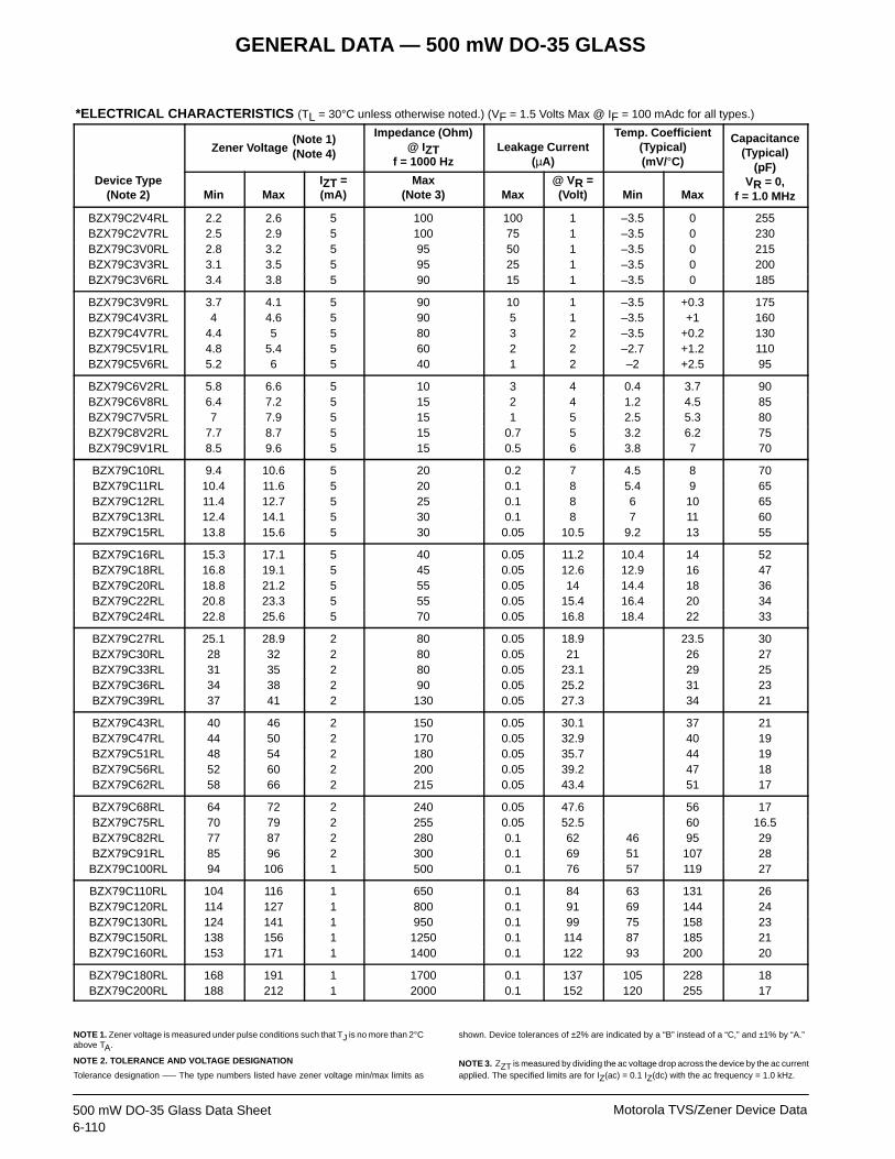
*ELECTRICAL CHARACTERISTICS (TL = 30°C unless otherwise noted.) (VF = 1.5 Volts Max @ IF = 100 mAdc for all types.)
D i T
Zener Voltage(Note 1)(Note 4)
Impedance (Ohm)@ IZT
f = 1000 HzLeakage Current
(µA)
Temp. Coefficient(Typical)(mV/°C)
Capacitance(Typical)
(pF)Device Type
(Note 2) Min MaxIZT =(mA)
Max(Note 3) Max
@ VR =(Volt) Min Max
(pF)VR = 0,
f = 1.0 MHz
BZX79C2V4RL 2.2 2.6 5 100 100 1 –3.5 0 255BZX79C2V7RL 2.5 2.9 5 100 75 1 –3.5 0 230BZX79C3V0RL 2.8 3.2 5 95 50 1 –3.5 0 215BZX79C3V3RL 3.1 3.5 5 95 25 1 –3.5 0 200BZX79C3V6RL 3.4 3.8 5 90 15 1 –3.5 0 185
BZX79C3V9RL 3.7 4.1 5 90 10 1 –3.5 +0.3 175BZX79C4V3RL 4 4.6 5 90 5 1 –3.5 +1 160BZX79C4V7RL 4.4 5 5 80 3 2 –3.5 +0.2 130BZX79C5V1RL 4.8 5.4 5 60 2 2 –2.7 +1.2 110BZX79C5V6RL 5.2 6 5 40 1 2 –2 +2.5 95
BZX79C6V2RL 5.8 6.6 5 10 3 4 0.4 3.7 90BZX79C6V8RL 6.4 7.2 5 15 2 4 1.2 4.5 85BZX79C7V5RL 7 7.9 5 15 1 5 2.5 5.3 80BZX79C8V2RL 7.7 8.7 5 15 0.7 5 3.2 6.2 75BZX79C9V1RL 8.5 9.6 5 15 0.5 6 3.8 7 70
BZX79C10RL 9.4 10.6 5 20 0.2 7 4.5 8 70BZX79C11RL 10.4 11.6 5 20 0.1 8 5.4 9 65BZX79C12RL 11.4 12.7 5 25 0.1 8 6 10 65BZX79C13RL 12.4 14.1 5 30 0.1 8 7 11 60BZX79C15RL 13.8 15.6 5 30 0.05 10.5 9.2 13 55
BZX79C16RL 15.3 17.1 5 40 0.05 11.2 10.4 14 52BZX79C18RL 16.8 19.1 5 45 0.05 12.6 12.9 16 47BZX79C20RL 18.8 21.2 5 55 0.05 14 14.4 18 36BZX79C22RL 20.8 23.3 5 55 0.05 15.4 16.4 20 34BZX79C24RL 22.8 25.6 5 70 0.05 16.8 18.4 22 33
BZX79C27RL 25.1 28.9 2 80 0.05 18.9 23.5 30BZX79C30RL 28 32 2 80 0.05 21 26 27BZX79C33RL 31 35 2 80 0.05 23.1 29 25BZX79C36RL 34 38 2 90 0.05 25.2 31 23BZX79C39RL 37 41 2 130 0.05 27.3 34 21
BZX79C43RL 40 46 2 150 0.05 30.1 37 21BZX79C47RL 44 50 2 170 0.05 32.9 40 19BZX79C51RL 48 54 2 180 0.05 35.7 44 19BZX79C56RL 52 60 2 200 0.05 39.2 47 18BZX79C62RL 58 66 2 215 0.05 43.4 51 17
BZX79C68RL 64 72 2 240 0.05 47.6 56 17BZX79C75RL 70 79 2 255 0.05 52.5 60 16.5BZX79C82RL 77 87 2 280 0.1 62 46 95 29BZX79C91RL 85 96 2 300 0.1 69 51 107 28BZX79C100RL 94 106 1 500 0.1 76 57 119 27
BZX79C110RL 104 116 1 650 0.1 84 63 131 26BZX79C120RL 114 127 1 800 0.1 91 69 144 24BZX79C130RL 124 141 1 950 0.1 99 75 158 23BZX79C150RL 138 156 1 1250 0.1 114 87 185 21BZX79C160RL 153 171 1 1400 0.1 122 93 200 20
BZX79C180RL 168 191 1 1700 0.1 137 105 228 18BZX79C200RL 188 212 1 2000 0.1 152 120 255 17
NOTE 1. Zener voltage is measured under pulse conditions such that TJ is no more than 2°Cabove TA.
NOTE 2. TOLERANCE AND VOLTAGE DESIGNATION
Tolerance designation —– The type numbers listed have zener voltage min/max limits as
shown. Device tolerances of ±2% are indicated by a “B” instead of a “C,” and ±1% by “A.”
NOTE 3. ZZT is measured by dividing the ac voltage drop across the device by the ac currentapplied. The specified limits are for IZ(ac) = 0.1 IZ(dc) with the ac frequency = 1.0 kHz.
GENERAL DATA — 500 mW DO-35 GLASS
Motorola TVS/Zener Device Data6-111
500 mW DO-35 Glass Data Sheet
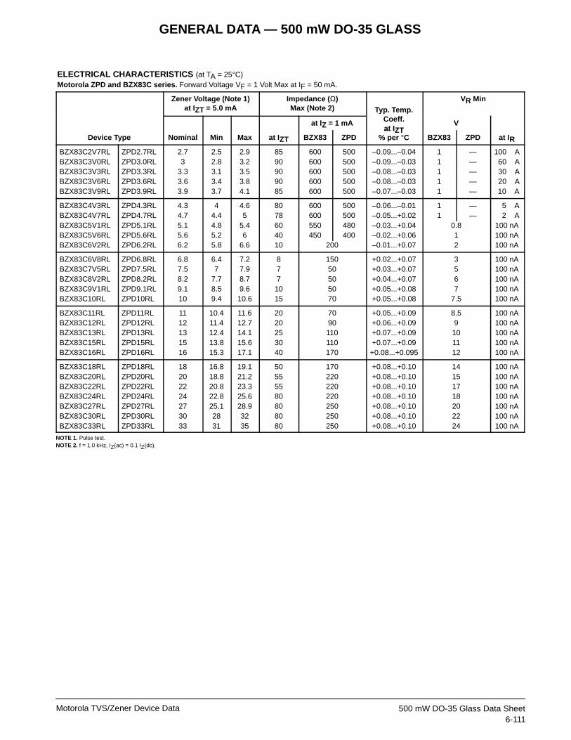
ELECTRICAL CHARACTERISTICS (at TA = 25°C)Motorola ZPD and BZX83C series. Forward Voltage VF = 1 Volt Max at IF = 50 mA.
Zener Voltage (Note 1)at IZT = 5.0 mA
Impedance ( Ω)Max (Note 2) Typ. Temp.
C ff
VR Min
at IZ = 1 mA
yp pCoeff.at IZT
V
Device Type Nominal Min Max at IZT BZX83 ZPDat IZT
% per °C BZX83 ZPD at IR
BZX83C2V7RL ZPD2.7RL 2.7 2.5 2.9 85 600 500 –0.09...–0.04 1 — 100 mABZX83C3V0RL ZPD3.0RL 3 2.8 3.2 90 600 500 –0.09...–0.03 1 — 160 mABZX83C3V3RL ZPD3.3RL 3.3 3.1 3.5 90 600 500 –0.08...–0.03 1 — 130 mABZX83C3V6RL ZPD3.6RL 3.6 3.4 3.8 90 600 500 –0.08...–0.03 1 — 120 mABZX83C3V9RL ZPD3.9RL 3.9 3.7 4.1 85 600 500 –0.07...–0.03 1 — 110 mA
BZX83C4V3RL ZPD4.3RL 4.3 4 4.6 80 600 500 –0.06...–0.01 1 — 115 mABZX83C4V7RL ZPD4.7RL 4.7 4.4 5 78 600 500 –0.05...+0.02 1 — 112 mABZX83C5V1RL ZPD5.1RL 5.1 4.8 5.4 60 550 480 –0.03...+0.04 0.8 100 nABZX83C5V6RL ZPD5.6RL 5.6 5.2 6 40 450 400 –0.02...+0.06 1 100 nABZX83C6V2RL ZPD6.2RL 6.2 5.8 6.6 10 200 –0.01...+0.07 2 100 nA
BZX83C6V8RL ZPD6.8RL 6.8 6.4 7.2 8 150 +0.02...+0.07 3 100 nABZX83C7V5RL ZPD7.5RL 7.5 7 7.9 7 50 +0.03...+0.07 5 100 nABZX83C8V2RL ZPD8.2RL 8.2 7.7 8.7 7 50 +0.04...+0.07 6 100 nABZX83C9V1RL ZPD9.1RL 9.1 8.5 9.6 10 50 +0.05...+0.08 7 100 nABZX83C10RL ZPD10RL 10 9.4 10.6 15 70 +0.05...+0.08 7.5 100 nA
BZX83C11RL ZPD11RL 11 10.4 11.6 20 70 +0.05...+0.09 8.5 100 nABZX83C12RL ZPD12RL 12 11.4 12.7 20 90 +0.06...+0.09 9 100 nABZX83C13RL ZPD13RL 13 12.4 14.1 25 110 +0.07...+0.09 10 100 nABZX83C15RL ZPD15RL 15 13.8 15.6 30 110 +0.07...+0.09 11 100 nABZX83C16RL ZPD16RL 16 15.3 17.1 40 170 +0.08...+0.095 12 100 nA
BZX83C18RL ZPD18RL 18 16.8 19.1 50 170 +0.08...+0.10 14 100 nABZX83C20RL ZPD20RL 20 18.8 21.2 55 220 +0.08...+0.10 15 100 nABZX83C22RL ZPD22RL 22 20.8 23.3 55 220 +0.08...+0.10 17 100 nABZX83C24RL ZPD24RL 24 22.8 25.6 80 220 +0.08...+0.10 18 100 nABZX83C27RL ZPD27RL 27 25.1 28.9 80 250 +0.08...+0.10 20 100 nABZX83C30RL ZPD30RL 30 28 32 80 250 +0.08...+0.10 22 100 nABZX83C33RL ZPD33RL 33 31 35 80 250 +0.08...+0.10 24 100 nA
NOTE 1. Pulse test.NOTE 2. f = 1.0 kHz, IZ(ac) = 0.1 IZ(dc).

@(Note 5)
GENERAL DATA — 500 mW DO-35 GLASS
Motorola TVS/Zener Device Data6-112500 mW DO-35 Glass Data Sheet
Designed for 250 mW applications requiring low leakage,low impedance. Same as 1N4099 through 1N4104 and1N4614 through 1N4627 except low noise test omitted.
• Voltage Range from 1.8 to 10 Volts• Zener Impedance and Zener Voltage Specified for Low-
Level Operation at IZT = 250 µA
ELECTRICAL CHARACTERISTICS (TA = 25°C unless otherwise specified. IZT = 250 µA and VF = 1 V Max @ IF = 200 mA for allELECTRICAL CHARACTERISTICS types)
TypeNumber(Note 1)
NominalZener Voltage
VZ(Note 2)(Volts)
Max ZenerImpedance
ZZT(Note 3)(Ohms)
MaxReverseCurrent
IR(µA)
TestVoltage
VR(Volts)
Max Zener CurrentIZM
(Note 4)(mA)
MZ4614 1.8 1200 7.5 1 120MZ4615 2 1250 5 1 110MZ4616 2.2 1300 4 1 100MZ4617 2.4 1400 2 1 95MZ4618 2.7 1500 1 1 90
MZ4619 3 1600 0.8 1 85MZ4620 3.3 1650 7.5 1.5 80MZ4621 3.6 1700 7.5 2 75MZ4622 3.9 1650 5 2 70MZ4623 4.3 1600 4 2 65
MZ4624 4.7 1550 10 3 60MZ4625 5.1 1500 10 3 55MZ4626 5.6 1400 10 4 50MZ4627 6.2 1200 10 5 45MZ4099 6.8 200 10 5.2 35
MZ4100 7.5 200 10 5.7 31.8MZ4101 8.2 200 1 6.3 29MZ4102 8.7 200 1 6.7 27.4MZ4103 9.1 200 1 7 26.2MZ4104 10 200 1 7.6 24.8
NOTE 1. TOLERANCE AND VOLTAGE DESIGNATIONThe type numbers shown have a standard tolerance of ±5% on the nominal zener voltage.
NOTE 2. ZENER VOLTAGE (VZ) MEASUREMENT
Nominal Zener Voltage is measured with the device junction in the thermal equilibrium withambient temperature of 25°C.
NOTE 3. ZENER IMPEDANCE (ZZT) DERIVATION
The zener impedance is derived from the 60 cycle ac voltage, which results when an ac cur-rent having an rms value equal to 10% of the dc zener current (IZT) is superimposed on IZT.
NOTE 4. MAXIMUM ZENER CURRENT RATINGS (IZM)
Maximum zener current ratings are based on maximum zener voltage of the individual units.
NOTE 5. REVERSE LEAKAGE CURRENT I RReverse leakage currents are guaranteed and are measured at VR as shown on the table.
NOTE 6. SPECIAL SELECTORS AVAILABLE INCLUDE:
A) Tighter voltage tolerances. Contact your nearest Motorola representative for more infor-mation.

GENERAL DATA — 500 mW DO-35 GLASS
Motorola TVS/Zener Device Data6-113
500 mW DO-35 Glass Data Sheet
Low Voltage Avalanche PassivatedSilicon Oxide Zener Regulator DiodesSame as 1N5520B through 1N5530B except low noise testspec omitted.• Low Maximum Regulation Factor• Low Zener Impedance• Low Leakage Current
ELECTRICAL CHARACTERISTICS (TA = 25°C unless otherwise specified. Based on dc measurements at thermal equilibrium;ELECTRICAL CHARACTERISTICS VF = 1.1 Max @ IF = 200 mA for all types.)
M l
NominalZener
TMax Zener
Max Reverse Leakage Current MaximumDC Zener Regulation Low
MotorolaType No.(Note 1)
ZenerVoltage
VZ @ IZTVolts
(Note 2)
TestCurrent
IZTmAdc
Max ZenerImpedanceZZT @ IZT
Ohms(Note 3)
IRµAdc
(Note 4) VR – Volts
DC ZenerCurrent
IZMmAdc
(Note 5)
RegulationFactor
∆VZVolts
(Note 6)
LowVZ
CurrentIZL
mAdc
MZ5520B 3.9 20 22 1 1 98 0.85 2.0MZ5521B 4.3 20 18 3 1.5 88 0.75 2.0MZ5522B 4.7 10 22 2 2 81 0.6 1.0MZ5523B 5.1 5 26 2 2.5 75 0.65 0.25MZ5524B 5.6 3 30 2 3.5 68 0.3 0.25
MZ5525B 6.2 1 30 1 5 61 0.2 0.01MZ5526B 6.8 1 30 1 6.2 56 0.1 0.01MZ5527B 7.5 1 35 0.5 6.8 51 0.05 0.01MZ5528B 8.2 1 40 0.5 7.5 46 0.05 0.01MZ5529B 9.1 1 45 0.1 8.2 42 0.05 0.01MZ5530B 10 1 60 0.05 9.1 38 0.1 0.01
NOTE 1. TOLERANCE AND VOLTAGE DESIGNATION
The “B” suffix type numbers listed are ±5% tolerance of nominal VZ.
NOTE 2. ZENER VOLTAGE (VZ) MEASUREMENT
Nominal zener voltage is measured with the device junction in thermal equilibrium with ambi-ent temperature of 25°C.
NOTE 3. ZENER IMPEDANCE (ZZ) DERIVATION
The zener impedance is derived from the 60 Hz ac voltage, which results when an ac currenthaving an rms value equal to 10% of the dc zener current (IZT) is superimposed on IZT.
NOTE 4. REVERSE LEAKAGE CURRENT I RReverse leakage currents are guaranteed and are measured at VR as shown on the table.
NOTE 5. MAXIMUM REGULATOR CURRENT (I ZM)
The maximum current shown is based on the maximum voltage of a ±5% type unit, therefore,it applies only to the “B” suffix device. The actual IZM for any device may not exceed the valueof 400 milliwatts divided by the actual VZ of the device.
NOTE 6. MAXIMUM REGULATION FACTOR ( ∆VZ)
∆VZ is the maximum difference between VZ at IZT and VZ at IZL measured with the devicejunction in thermal equilibrium.
NOTE 7. SPECIAL SELECTORS AVAILABLE INCLUDE:
A) Tighter voltage tolerances. Contact your nearest Motorola representative for more infor-mation.

GENERAL DATA — 500 mW DO-35 GLASS
Motorola TVS/Zener Device Data6-114500 mW DO-35 Glass Data Sheet
500 mW DO-35 Glass
MULTIPLE PACKAGE QUANTITY (MPQ)REQUIREMENTS
Zener Voltage Regulator Diodes — Axial Leaded
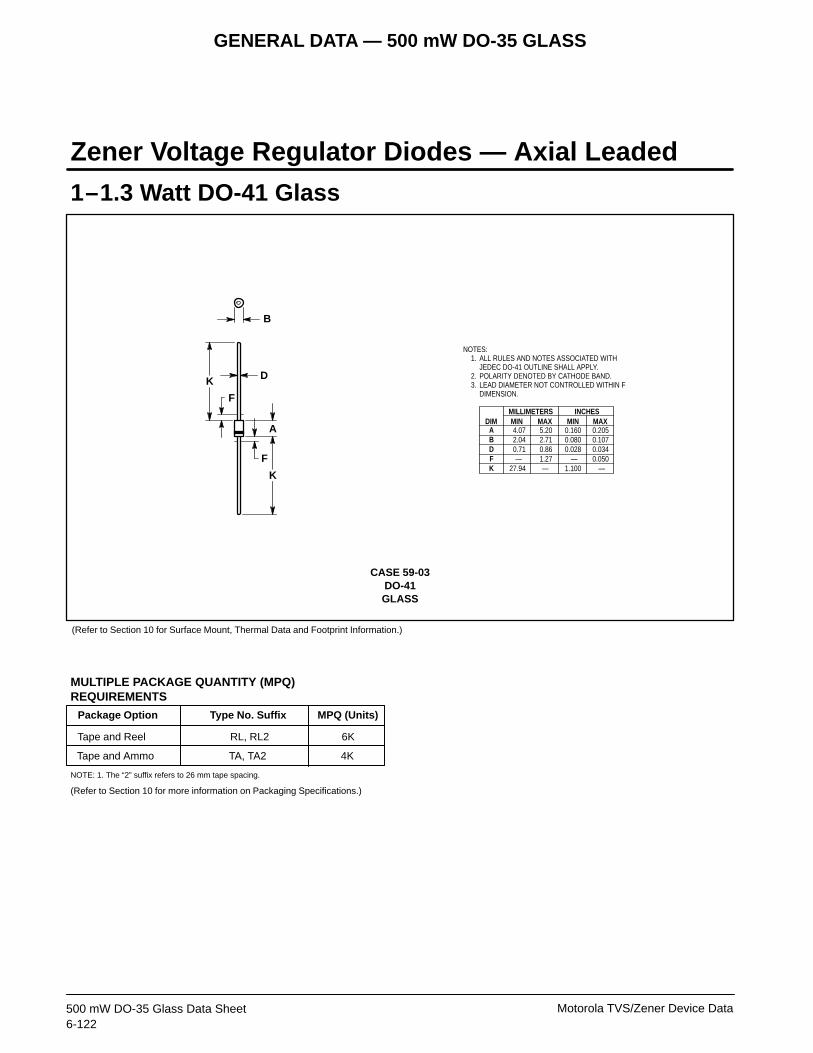
CASE 299-02DO-204AH
GLASS
(Refer to Section 10 for Surface Mount, Thermal Data and Footprint Information.)
Refer to Section 10 for more information on Packaging Specifications.
MIN MINMAX MAXMILLIMETERS INCHES
DIM3.051.520.46—
25.40
5.082.290.561.2738.10
0.1200.0600.018—
1.000
0.2000.0900.0220.0501.500
ABDFK
All JEDEC dimensions and notes apply.
NOTES:1. PACKAGE CONTOUR OPTIONAL WITHIN A AND B
HEAT SLUGS, IF ANY, SHALL BE INCLUDEDWITHIN THIS CYLINDER, BUT NOT SUBJECT TOTHE MINIMUM LIMIT OF B.
2. LEAD DIAMETER NOT CONTROLLED IN ZONE FTO ALLOW FOR FLASH, LEAD FINISH BUILDUPAND MINOR IRREGULARITIES OTHER THANHEAT SLUGS.
3. POLARITY DENOTED BY CATHODE BAND.4. DIMENSIONING AND TOLERANCING PER ANSI
Y14.5M, 1982.
B
A
KD
F
F
K
Package Option
Tape and Reel 5K
Type No. Suffix
RL, RL2(1)
MPQ (Units)
Tape and Ammo TA, TA2(1) 5K
NOTES: 1. The “2” suffix refers to 26 mm tape spacing.NOTES: 2. Radial Tape and Reel may be available. Please contact your MotorolaNOTES: 2. representative.
GENERAL DATA — 500 mW DO-35 GLASS
Motorola TVS/Zener Device Data6-115
500 mW DO-35 Glass Data Sheet
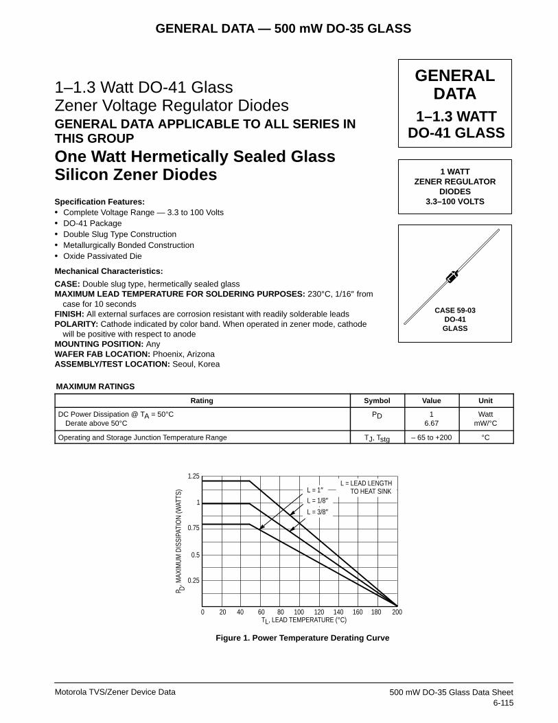
1–1.3 Watt DO-41 GlassZener Voltage Regulator DiodesGENERAL DATA APPLICABLE TO ALL SERIES INTHIS GROUP
One Watt Hermetically Sealed GlassSilicon Zener Diodes
Specification Features:• Complete Voltage Range — 3.3 to 100 Volts• DO-41 Package• Double Slug Type Construction• Metallurgically Bonded Construction• Oxide Passivated Die
Mechanical Characteristics:
CASE: Double slug type, hermetically sealed glassMAXIMUM LEAD TEMPERATURE FOR SOLDERING PURPOSES: 230°C, 1/16″ from
case for 10 secondsFINISH: All external surfaces are corrosion resistant with readily solderable leadsPOLARITY: Cathode indicated by color band. When operated in zener mode, cathode
will be positive with respect to anodeMOUNTING POSITION: AnyWAFER FAB LOCATION: Phoenix, ArizonaASSEMBLY/TEST LOCATION: Seoul, Korea
MAXIMUM RATINGS
Rating Symbol Value Unit
DC Power Dissipation @ TA = 50°CDerate above 50°C
PD 16.67
WattmW/°C
Operating and Storage Junction Temperature Range TJ, Tstg – 65 to +200 °C
Figure 1. Power Temperature Derating Curve
TL, LEAD TEMPERATURE (°C)
P ,
MAX
IMU
M D
ISSI
PATI
ON
(WAT
TS)
D
0 20 40 60 20080 100 120 140 160 180
0.25
0.5
0.75
1
1.25L = LEAD LENGTH TO HEAT SINK
L = 3/8″L = 1/8″L = 1″
GENERALDATA
CASE 59-03DO-41GLASS
1–1.3 WATTDO-41 GLASS
1 WATTZENER REGULATOR
DIODES3.3–100 VOLTS
GENERAL DATA — 500 mW DO-35 GLASS
Motorola TVS/Zener Device Data6-116500 mW DO-35 Glass Data Sheet
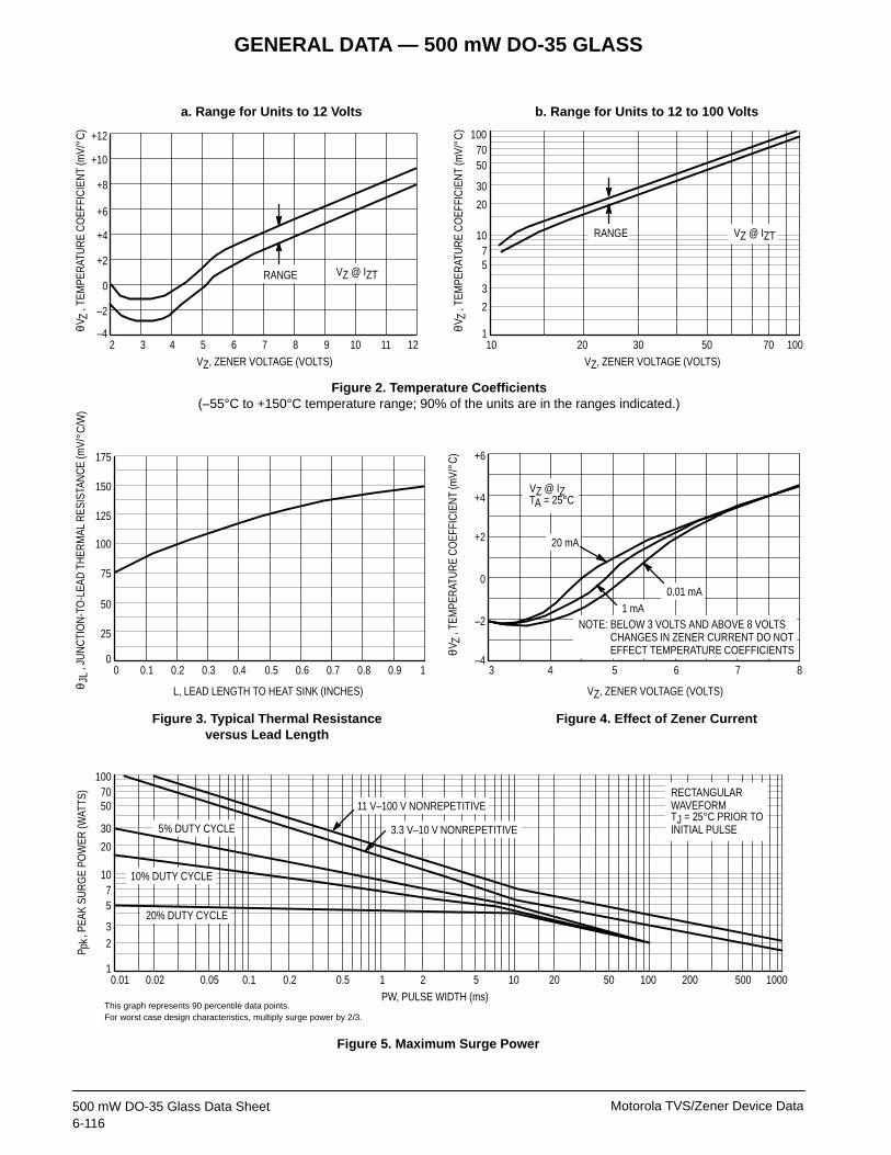
Figure 2. Temperature Coefficients(–55°C to +150°C temperature range; 90% of the units are in the ranges indicated.)
a. Range for Units to 12 Volts b. Range for Units to 12 to 100 Volts
+12
+10
+8
+6
+4
+2
0
–2
–42 3 4 5 6 7 8 9 10 11 12
VZ, ZENER VOLTAGE (VOLTS)
θVZ
, TEM
PER
ATU
RE
CO
EFFI
CIE
NT
(mV/
°C) 100
7050
30
20
1075
3
2
110 20 30 50 70 100
VZ, ZENER VOLTAGE (VOLTS)
θVZ
, TEM
PER
ATU
RE
CO
EFFI
CIE
NT
(mV/
°C)
VZ @ IZTRANGE
RANGE VZ @ IZT
Figure 3. Typical Thermal Resistanceversus Lead Length
Figure 4. Effect of Zener Current
175
150
125
100
75
50
25
00 0.1 0.2 0.3 0.4 0.5 0.6 0.7 0.8 0.9 1
L, LEAD LENGTH TO HEAT SINK (INCHES)θ JL
, JU
NC
TIO
N-T
O-L
EAD
TH
ERM
AL R
ESIS
TAN
CE
(mV/
°C/W
)
θVZ
, TEM
PER
ATU
RE
CO
EFFI
CIE
NT
(mV/
°C) +6
+4
+2
0
–2
–43 4 5 6 7 8
VZ, ZENER VOLTAGE (VOLTS)
VZ @ IZTA = 25°C
20 mA
0.01 mA1 mA
NOTE: BELOW 3 VOLTS AND ABOVE 8 VOLTSNOTE: CHANGES IN ZENER CURRENT DO NOTNOTE: EFFECT TEMPERATURE COEFFICIENTS
Figure 5. Maximum Surge Power
1007050
30
20
1075
32
10.01 0.02 0.05 0.1 0.2 0.5 1 2 5 10 20 50 100 200 500 1000
PW, PULSE WIDTH (ms)This graph represents 90 percentile data points.For worst case design characteristics, multiply surge power by 2/3.
P pk,
PEA
K SU
RG
E PO
WER
(WAT
TS)
11 V–100 V NONREPETITIVE
3.3 V–10 V NONREPETITIVE5% DUTY CYCLE
10% DUTY CYCLE
20% DUTY CYCLE
RECTANGULARWAVEFORMTJ = 25°C PRIOR TOINITIAL PULSE

GENERAL DATA — 500 mW DO-35 GLASS
Motorola TVS/Zener Device Data6-117
500 mW DO-35 Glass Data Sheet
Figure 10. Typical Forward Characteristics
VF, FORWARD VOLTAGE (VOLTS)
0.4 0.5 0.6 0.7 0.8 0.9 1 1.1
1000500
200
100
50
20
10
5
2
1
I F, F
OR
WAR
D C
UR
REN
T (m
A)
MAXIMUM
150°C
75°C
0°C
25°C
Figure 6. Effect of Zener Currenton Zener Impedance
Figure 7. Effect of Zener Voltageon Zener Impedance
Figure 9. Typical Capacitance versus V Z
Figure 8. Typical Leakage Current
1000500
200
100
50
20
10
5
2
10.1 0.2 0.5 1 2 5 10 20 50 100
IZ, ZENER CURRENT (mA)
ZZ
, DYN
AMIC
IMPE
DAN
CE
(OH
MS)
1000700500
200
1007050
20
1075
2
11 2 100
VZ, ZENER CURRENT (mA)3 5 7 10 20 30 50 70
ZZ
, DYN
AMIC
IMPE
DAN
CE
(OH
MS)
1000070005000
2000
1000700500
200
1007050
20
1075
2
10.70.5
0.2
0.10.070.05
0.02
0.010.0070.005
0.002
0.001
I R, L
EAKA
GE
CU
RR
ENT
(µA)
3 4 5 6 7 8 9 10 11 12 13 14 15
VZ, NOMINAL ZENER VOLTAGE (VOLTS)
+25°C
+125°C
TYPICAL LEAKAGE CURRENTAT 80% OF NOMINALBREAKDOWN VOLTAGE
TJ = 25°CiZ(rms) = 0.1 IZ(dc)f = 60 Hz
6.2 V
27 V
VZ = 2.7 V
47 V
TJ = 25°CiZ(rms) = 0.1 IZ(dc)f = 60 Hz
20 mA
5 mA
IZ = 1 mA
0 V BIAS
1 V BIAS
400300
200
100
50
20
108
41 2 5 10 20 50 100
VZ, NOMINAL VZ (VOLTS)
C, C
APAC
ITAN
CE
(pF)
50% OF BREAKDOWN BIAS
MINIMUM

GENERAL DATA — 500 mW DO-35 GLASS
Motorola TVS/Zener Device Data6-118500 mW DO-35 Glass Data Sheet
APPLICATION NOTE
Since the actual voltage available from a given zener diodeis temperature dependent, it is necessary to determine junc-tion temperature under any set of operating conditions in orderto calculate its value. The following procedure is recom-mended:
Lead Temperature, TL, should be determined from:
TL = θLAPD + TA.
θLA is the lead-to-ambient thermal resistance (°C/W) and PD isthe power dissipation. The value for θLA will vary and dependson the device mounting method. θLA is generally 30 to 40°C/Wfor the various clips and tie points in common use and forprinted circuit board wiring.
The temperature of the lead can also be measured using athermocouple placed on the lead as close as possible to the tiepoint. The thermal mass connected to the tie point is normallylarge enough so that it will not significantly respond to heatsurges generated in the diode as a result of pulsed operationonce steady-state conditions are achieved. Using the mea-sured value of TL, the junction temperature may be deter-mined by:
TJ = TL + ∆TJL.∆TJL is the increase in junction temperature above the lead
temperature and may be found as follows:
∆TJL = θJLPD.
θJL may be determined from Figure 3 for dc power condi-tions. For worst-case design, using expected limits of IZ, limitsof PD and the extremes of TJ(∆TJ) may be estimated. Changesin voltage, VZ, can then be found from:
∆V = θVZ ∆TJ.
θVZ, the zener voltage temperature coefficient, is found fromFigure 2.
Under high power-pulse operation, the zener voltage willvary with time and may also be affected significantly by thezener resistance. For best regulation, keep current excursionsas low as possible.
Surge limitations are given in Figure 5. They are lower thanwould be expected by considering only junction temperature,as current crowding effects cause temperatures to be ex-tremely high in small spots, resulting in device degradationshould the limits of Figure 5 be exceeded.

GENERAL DATA — 500 mW DO-35 GLASS
Motorola TVS/Zener Device Data6-119
500 mW DO-35 Glass Data Sheet
*ELECTRICAL CHARACTERISTICS (TA = 25°C unless otherwise noted) VF = 1.2 V Max, IF = 200 mA for all types.
JEDEC
NominalZener Voltage Test
Maximum Zener Impedance (Note 4) Leakage CurrentSurge Current @
JEDECType No.(Note 1)
Zener VoltageVZ @ IZT
Volts(Notes 2 and 3)
TestCurrent
IZTmA
ZZT @ IZTOhms
ZZK @ IZKOhms
IZKmA
IRµA Max
VRVolts
Surge Current @TA = 25°C
ir – mA(Note 5)
1N4728A 3.3 76 10 400 1 100 1 13801N4729A 3.6 69 10 400 1 100 1 12601N4730A 3.9 64 9 400 1 50 1 11901N4731A 4.3 58 9 400 1 10 1 10701N4732A 4.7 53 8 500 1 10 1 970
1N4733A 5.1 49 7 550 1 10 1 8901N4734A 5.6 45 5 600 1 10 2 8101N4735A 6.2 41 2 700 1 10 3 7301N4736A 6.8 37 3.5 700 1 10 4 6601N4737A 7.5 34 4 700 0.5 10 5 605
1N4738A 8.2 31 4.5 700 0.5 10 6 5501N4739A 9.1 28 5 700 0.5 10 7 5001N4740A 10 25 7 700 0.25 10 7.6 4541N4741A 11 23 8 700 0.25 5 8.4 4141N4742A 12 21 9 700 0.25 5 9.1 380
1N4743A 13 19 10 700 0.25 5 9.9 3441N4744A 15 17 14 700 0.25 5 11.4 3041N4745A 16 15.5 16 700 0.25 5 12.2 2851N4746A 18 14 20 750 0.25 5 13.7 2501N4747A 20 12.5 22 750 0.25 5 15.2 225
1N4748A 22 11.5 23 750 0.25 5 16.7 2051N4749A 24 10.5 25 750 0.25 5 18.2 1901N4750A 27 9.5 35 750 0.25 5 20.6 1701N4751A 30 8.5 40 1000 0.25 5 22.8 1501N4752A 33 7.5 45 1000 0.25 5 25.1 135
1N4753A 36 7 50 1000 0.25 5 27.4 1251N4754A 39 6.5 60 1000 0.25 5 29.7 1151N4755A 43 6 70 1500 0.25 5 32.7 1101N4756A 47 5.5 80 1500 0.25 5 35.8 951N4757A 51 5 95 1500 0.25 5 38.8 90
1N4758A 56 4.5 110 2000 0.25 5 42.6 801N4759A 62 4 125 2000 0.25 5 47.1 701N4760A 68 3.7 150 2000 0.25 5 51.7 651N4761A 75 3.3 175 2000 0.25 5 56 601N4762A 82 3 200 3000 0.25 5 62.2 551N4763A 91 2.8 250 3000 0.25 5 69.2 501N4764A 100 2.5 350 3000 0.25 5 76 45
*Indicates JEDEC Registered Data.
NOTE 1. TOLERANCE AND TYPE NUMBER DESIGNATION
The JEDEC type numbers listed have a standard tolerance on the nominal zener voltage of±5%. C for ±2%, D for ±1%.
NOTE 2. SPECIALS AVAILABLE INCLUDE:
Nominal zener voltages between the voltages shown and tighter voltage tolerances.
For detailed information on price, availability, and delivery, contact your nearest Motorola rep-resentative.
NOTE 3. ZENER VOLTAGE (VZ) MEASUREMENT
Motorola guarantees the zener voltage when measured at 90 seconds while maintaining thelead temperature (TL) at 30°C ± 1°C, 3/8″ from the diode body.
NOTE 4. ZENER IMPEDANCE (ZZ) DERIVATION
The zener impedance is derived from the 60 cycle ac voltage, which results when an ac cur-rent having an rms value equal to 10% of the dc zener current (IZT or IZK) is superimposedon IZT or IZK.
NOTE 5. SURGE CURRENT (ir) NON-REPETITIVE
The rating listed in the electrical characteristics table is maximum peak, non-repetitive, re-verse surge current of 1/2 square wave or equivalent sine wave pulse of 1/120 second dura-tion superimposed on the test current, IZT, per JEDEC registration; however, actual devicecapability is as described in Figure 5 of the General Data — DO-41 Glass.

GENERAL DATA — 500 mW DO-35 GLASS
Motorola TVS/Zener Device Data6-120500 mW DO-35 Glass Data Sheet
ELECTRICAL CHARACTERISTICS (TA = 25°C unless otherwise noted.) (VF = 1.2 V Max, IF = 200 mA for all types.)
T
Zener VoltageVZT (V)
(Notes 2 and 3) TestC t
Zener ImpedanceZZ (ohms)(Note 4)
LeakageCurrent
(µA)Surge
CurrentT 25 C
Type VZ VZCurrent
IZT MaxMax at IZ IR
TA = 25°Cir (mA)Type
(Note 1)VZMin
VZMax
IZT(mA)
Maxat IZT (mA) VR (V)
IRMax
ir (mA)(Note 5)
BZX85C3V3RL 3.1 3.5 80 20 400 1 1 60 1380BZX85C3V6RL 3.4 3.8 60 15 500 1 1 30 1260BZX85C3V9RL 3.7 4.1 60 15 500 1 1 5 1190BZX85C4V3RL 4 4.6 50 13 500 1 1 3 1070BZX85C4V7RL 4.4 5 45 13 600 1 1.5 3 970
BZX85C5V1RL 4.8 5.4 45 10 500 1 2 1 890BZX85C5V6RL 5.2 6 45 7 400 1 2 1 810BZX85C6V2RL 5.8 6.6 35 4 300 1 3 1 730BZX85C6V8RL 6.4 7.2 35 3.5 300 1 4 1 660BZX85C7V5RL 7 7.9 35 3 200 0.5 4.5 1 605
BZX85C8V2RL 7.7 8.7 25 5 200 0.5 5 1 550BZX85C9V1RL 8.5 9.6 25 5 200 0.5 6.5 1 500BZX85C10RL 9.4 10.6 25 7 200 0.5 7 0.5 454BZX85C11RL 10.4 11.6 20 8 300 0.5 7.7 0.5 414BZX85C12RL 11.4 12.7 20 9 350 0.5 8.4 0.5 380
BZX85C13RL 12.4 14.1 20 10 400 0.5 9.1 0.5 344BZX85C15RL 13.8 15.6 15 15 500 0.5 10.5 0.5 304BZX85C16RL 15.3 17.1 15 15 500 0.5 11 0.5 285BZX85C18RL 16.8 19.1 15 20 500 0.5 12.5 0.5 250BZX85C20RL 18.8 21.2 10 24 600 0.5 14 0.5 225
BZX85C22RL 20.8 23.3 10 25 600 0.5 15.5 0.5 205BZX85C24RL 22.8 25.6 10 25 600 0.5 17 0.5 190BZX85C27RL 25.1 28.9 8 30 750 0.25 19 0.5 170BZX85C30RL 28 32 8 30 1000 0.25 21 0.5 150BZX85C33RL 31 35 8 35 1000 0.25 23 0.5 135
BZX85C36RL 34 38 8 40 1000 0.25 25 0.5 125BZX85C39RL 37 41 6 45 1000 0.25 27 0.5 115BZX85C43RL 40 46 6 50 1000 0.25 30 0.5 110BZX85C47RL 44 50 4 90 1500 0.25 33 0.5 95BZX85C51RL 48 54 4 115 1500 0.25 36 0.5 90
BZX85C56RL 52 60 4 120 2000 0.25 39 0.5 80BZX85C62RL 58 66 4 125 2000 0.25 43 0.5 70BZX85C68RL 64 72 4 130 2000 0.25 47 0.5 65BZX85C75RL 70 80 4 150 2000 0.25 51 0.5 60BZX85C82RL 77 87 2.7 200 3000 0.25 56 0.5 55
BZX85C91RL 85 96 2.7 250 3000 0.25 62 0.5 50BZX85C100RL 96 106 2.7 350 3000 0.25 68 0.5 45
NOTE 1. TOLERANCE AND TYPE NUMBER DESIGNATION
The type numbers listed have zener voltage min/max limits as shown. Device tolerance of±2% are indicated by a “B” instead of “C.”
NOTE 2. SPECIALS AVAILABLE INCLUDE:
Nominal zener voltages between the voltages shown and tighter voltage tolerances.
For detailed information on price, availability, and delivery, contact your nearest Motorola rep-resentative.
NOTE 3. ZENER VOLTAGE (VZ) MEASUREMENTVZ is measured after the test current has been applied to 40 ± 10 msec., while maintainingthe lead temperature (TL) at 30°C ± 1°C, 3/8″ from the diode body.
NOTE 4. ZENER IMPEDANCE (ZZ) DERIVATION
The zener impedance is derived from the 1 kHz cycle ac voltage, which results when an accurrent having an rms value equal to 10% of the dc zener current (IZT) or (IZK) is superim-posed on IZT or IZK.
NOTE 5. SURGE CURRENT (ir) NON-REPETITIVE
The rating listed in the electrical characteristics table is maximum peak, non-repetitive, re-verse surge current of 1/2 square wave or equivalent sine wave pulse of 1/120 second dura-tion superimposed on the test current IZT. However, actual device capability is as describedin Figure 5 of General Data DO-41 glass.
GENERAL DATA — 500 mW DO-35 GLASS
Motorola TVS/Zener Device Data6-121
500 mW DO-35 Glass Data Sheet
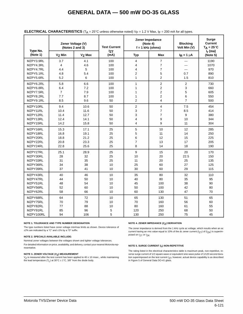
ELECTRICAL CHARACTERISTICS (TA = 25°C unless otherwise noted) VF = 1.2 V Max, IF = 200 mA for all types.
Type No
Zener Voltage (V)(Notes 2 and 3) Test Current
IZT
Zener Impedance(Note 4)
f = 1 kHz (ohms)Blocking
Volt Min (V)
SurgeCurrent
TA = 25°Ci (ma)Type No.
(Note 1) VZ Min VZ MaxIZT
(mA) Typ Max IR = 1 µAir (ma)
(Note 5)
MZPY3.9RL 3.7 4.1 100 4 7 — 1190MZPY4.3RL 4 4.6 100 4 7 — 1070MZPY4.7RL 4.4 5 100 4 7 — 970MZPY5.1RL 4.8 5.4 100 2 5 0.7 890MZPY5.6RL 5.2 6 100 1 2 1.5 810
MZPY6.2RL 5.8 6.6 100 1 2 2 730MZPY6.8RL 6.4 7.2 100 1 2 3 660MZPY7.5RL 7 7.9 100 1 2 5 605MZPY8.2RL 7.7 8.7 100 1 2 6 550MZPY9.1RL 8.5 9.6 50 2 4 7 500
MZPY10RL 9.4 10.6 50 2 4 7.5 454MZPY11RL 10.4 11.6 50 3 7 8.5 414MZPY12RL 11.4 12.7 50 3 7 9 380MZPY13RL 12.4 14.1 50 4 9 10 344MZPY15RL 14.2 15.8 50 4 9 11 304
MZPY16RL 15.3 17.1 25 5 10 12 285MZPY18RL 16.8 19.1 25 5 11 14 250MZPY20RL 18.8 21.2 25 6 12 15 225MZPY22RL 20.8 23.3 25 7 13 17 205MZPY24RL 22.8 25.6 25 8 14 18 190
MZPY27RL 25.1 28.9 25 9 15 20 170MZPY30RL 28 32 25 10 20 22.5 150MZPY33RL 31 35 25 11 20 25 135MZPY36RL 34 38 10 25 60 27 125MZPY39RL 37 41 10 30 60 29 115
MZPY43RL 40 46 10 35 80 32 110MZPY47RL 44 50 10 40 80 35 95MZPY51RL 48 54 10 45 100 38 90MZPY56RL 52 60 10 50 100 42 80MZPY62RL 58 66 10 60 130 47 70
MZPY68RL 64 72 10 65 130 51 65MZPY75RL 70 79 10 70 160 56 60MZPY82RL 77 88 10 80 160 61 55MZPY91RL 85 96 5 120 250 68 50MZPY100RL 94 106 5 130 250 75 45
NOTE 1. TOLERANCE AND TYPE NUMBER DESIGNATION
The type numbers listed have zener voltage min/max limits as shown. Device tolerance of±2% are indicated by a “C” and ±1% by a “D” suffix.
NOTE 2. SPECIALS AVAILABLE INCLUDE:
Nominal zener voltages between the voltages shown and tighter voltage tolerances.
For detailed information on price, availability, and delivery, contact your nearest Motorola rep-resentative.
NOTE 3. ZENER VOLTAGE (VZ) MEASUREMENTVZ is measured after the test current has been applied to 40 ± 10 msec., while maintainingthe lead temperature (TL) at 30°C ± 1°C, 3/8″ from the diode body.
NOTE 4. ZENER IMPEDANCE (ZZ) DERIVATION
The zener impedance is derived from the 1 kHz cycle ac voltage, which results when an accurrent having an rms value equal to 10% of the dc zener current (IZT) of (IZK) is superim-posed on IZT or IZK.
NOTE 5. SURGE CURRENT (ir) NON-REPETITIVE
The rating listed in the electrical characteristics table is maximum peak, non-repetitive, re-verse surge current of 1/2 square wave or equivalent sine wave pulse of 1/120 second dura-tion superimposed on the test current IZT, however, actual device capability is as describedin Figure 5 of General Data DO-41 glass.
GENERAL DATA — 500 mW DO-35 GLASS
Motorola TVS/Zener Device Data6-122500 mW DO-35 Glass Data Sheet
1–1.3 Watt DO-41 Glass
MULTIPLE PACKAGE QUANTITY (MPQ)REQUIREMENTS
Zener Voltage Regulator Diodes — Axial Leaded
CASE 59-03DO-41GLASS
(Refer to Section 10 for Surface Mount, Thermal Data and Footprint Information.)
(Refer to Section 10 for more information on Packaging Specifications.)
Package Option
Tape and Reel 6K
Type No. Suffix
RL, RL2
MPQ (Units)
Tape and Ammo TA, TA2 4K
NOTES:1. ALL RULES AND NOTES ASSOCIATED WITH
JEDEC DO-41 OUTLINE SHALL APPLY.2. POLARITY DENOTED BY CATHODE BAND.3. LEAD DIAMETER NOT CONTROLLED WITHIN F
DIMENSION.
K
K
F
A
F
D
MIN MINMAX MAXMILLIMETERS INCHES
DIM4.072.040.71—
27.94
5.202.710.861.27—
0.1600.0800.028
— 1.100
0.2050.1070.0340.050
—
ABDFK
B
NOTE: 1. The “2” suffix refers to 26 mm tape spacing.

GENERAL DATA — 500 mW DO-35 GLASS
Motorola TVS/Zener Device Data6-123
500 mW DO-35 Glass Data Sheet
1 to 3 Watt DO-41 Surmetic 30Zener Voltage Regulator DiodesGENERAL DATA APPLICABLE TO ALL SERIES INTHIS GROUP
1 to 3 Watt Surmetic 30Silicon Zener Diodes. . . a complete series of 1 to 3 Watt Zener Diodes with limits and operating characteristicsthat reflect the superior capabilities of silicon-oxide-passivated junctions. All this in anaxial-lead, transfer-molded plastic package offering protection in all common environmen-tal conditions.
Specification Features:• Surge Rating of 98 Watts @ 1 ms• Maximum Limits Guaranteed On Up To Six Electrical Parameters• Package No Larger Than the Conventional 1 Watt Package
Mechanical Characteristics:
CASE: Void-free, transfer-molded, thermosetting plasticFINISH: All external surfaces are corrosion resistant and leads are readily solderablePOLARITY: Cathode indicated by color band. When operated in zener mode, cathode
will be positive with respect to anodeMOUNTING POSITION: AnyWEIGHT: 0.4 gram (approx)WAFER FAB LOCATION: Phoenix, ArizonaASSEMBLY/TEST LOCATION: Seoul, Korea
MAXIMUM RATINGS
Rating Symbol Value Unit
DC Power Dissipation @ TL = 75°CLead Length = 3/8″Derate above 75°C
PD 3
24
Watts
mW/°C
DC Power Dissipation @ TA = 50°CDerate above 50°C
PD 16.67
WattmW/°C
Operating and Storage Junction Temperature Range TJ, Tstg – 65 to +200 °C
GENERALDATA
CASE 59-03DO-41
PLASTIC
1–3 WATTDO-41
SURMETIC 30
1 TO 3 WATTZENER REGULATOR
DIODES3.3–400 VOLTS
Figure 1. Power Temperature Derating Curve
TL, LEAD TEMPERATURE (°C)
P ,
MAX
IMU
M D
ISSI
PATI
ON
(WAT
TS)
D
0 20 40 60 20080 100 120 140 160 1800
1
2
3
4
5
L = 1/8″
L = 3/8″
L = 1″
L = LEAD LENGTH TO HEAT SINK
GENERAL DATA — 500 mW DO-35 GLASS
Motorola TVS/Zener Device Data6-124500 mW DO-35 Glass Data Sheet
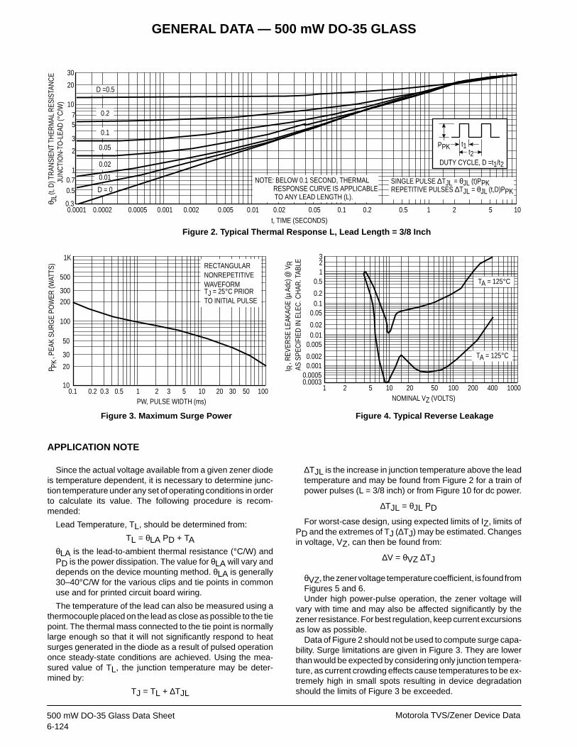
t, TIME (SECONDS)0.0001 0.0002 0.0005 0.001 0.002 0.005 0.01 0.02 0.05 0.1 0.2 0.5 1 2 5 10
0.3
0.50.7
1
2
3
57
10
20
30
D =0.5
0.2
0.1
0.05
0.01
D = 0
DUTY CYCLE, D =t1/t2
θ JL(t,
D) T
RAN
SIEN
T TH
ERM
AL R
ESIS
TAN
CE
JU
NC
TIO
N-T
O-L
EAD
( C
/W)
°
PPK t1
NOTE: BELOW 0.1 SECOND, THERMAL RESPONSE CURVE IS APPLICABLE
TO ANY LEAD LENGTH (L).
SINGLE PULSE ∆TJL = θJL (t)PPKREPETITIVE PULSES ∆TJL = θJL (t,D)PPK
t20.02
10
20
30
50
100
200
300
500
1K
0.1 0.2 0.3 0.5 1 2 3 5 10 20 30 50 100PW, PULSE WIDTH (ms)
P
, PE
AK S
UR
GE
POW
ER (W
ATTS
)PK
1 2 5 10 20 50 100 200 400 10000.00030.0005
0.0010.002
0.0050.010.02
0.050.10.2
0.5123
TA = 125°C
TA = 125°C
NOMINAL VZ (VOLTS)
AS S
PEC
IFIE
D IN
ELE
C. C
HAR
. TAB
LE
Figure 2. Typical Thermal Response L, Lead Length = 3/8 Inch
Figure 3. Maximum Surge Power Figure 4. Typical Reverse Leakage
I R, R
EVER
SE L
EAKA
GE
(µAd
c) @
VRRECTANGULAR
NONREPETITIVEWAVEFORMTJ = 25°C PRIORTO INITIAL PULSE
APPLICATION NOTE
Since the actual voltage available from a given zener diodeis temperature dependent, it is necessary to determine junc-tion temperature under any set of operating conditions in orderto calculate its value. The following procedure is recom-mended:
Lead Temperature, TL, should be determined from:
TL = θLA PD + TAθLA is the lead-to-ambient thermal resistance (°C/W) andPD is the power dissipation. The value for θLA will vary anddepends on the device mounting method. θLA is generally30–40°C/W for the various clips and tie points in commonuse and for printed circuit board wiring.
The temperature of the lead can also be measured using athermocouple placed on the lead as close as possible to the tiepoint. The thermal mass connected to the tie point is normallylarge enough so that it will not significantly respond to heatsurges generated in the diode as a result of pulsed operationonce steady-state conditions are achieved. Using the mea-sured value of TL, the junction temperature may be deter-mined by:
TJ = TL + ∆TJL
∆TJL is the increase in junction temperature above the leadtemperature and may be found from Figure 2 for a train ofpower pulses (L = 3/8 inch) or from Figure 10 for dc power.
∆TJL = θJL PD
For worst-case design, using expected limits of IZ, limits ofPD and the extremes of TJ (∆TJ) may be estimated. Changesin voltage, VZ, can then be found from:
∆V = θVZ ∆TJ
θVZ, the zener voltage temperature coefficient, is found fromFigures 5 and 6.Under high power-pulse operation, the zener voltage will
vary with time and may also be affected significantly by thezener resistance. For best regulation, keep current excursionsas low as possible.
Data of Figure 2 should not be used to compute surge capa-bility. Surge limitations are given in Figure 3. They are lowerthan would be expected by considering only junction tempera-ture, as current crowding effects cause temperatures to be ex-tremely high in small spots resulting in device degradationshould the limits of Figure 3 be exceeded.

GENERAL DATA — 500 mW DO-35 GLASS
Motorola TVS/Zener Device Data6-125
500 mW DO-35 Glass Data Sheet
Figure 5. Units To 12 Volts Figure 6. Units 10 To 400 Volts
Figure 7. V Z = 3.3 thru 10 Volts Figure 8. V Z = 12 thru 82 Volts
Figure 9. V Z = 100 thru 400 Volts Figure 10. Typical Thermal Resistance
ZENER VOLTAGE versus ZENER CURRENT(Figures 7, 8 and 9)
TEMPERATURE COEFFICIENT RANGES(90% of the Units are in the Ranges Indicated)
VZ, ZENER VOLTAGE @ IZT (VOLTS)3 4 5 6 7 8 9 10 11 12
10
8
6
4
2
0
–2
–4
RANGE
, TEM
PER
ATU
RE
CO
EFFI
CIE
NT
(mV/
C) @
IZT
VZ°
θ
1000
500
200
100
50
20
1010 20 50 100 200 400 1000
VZ, ZENER VOLTAGE @ IZT (VOLTS)
, TEM
PER
ATU
RE
CO
EFFI
CIE
NT
(mV/
C) @
I ZT
VZ°
θ
0 1 2 3 4 5 6 7 8 9 10
100
503020
10
1
0.50.30.2
0.1
VZ, ZENER VOLTAGE (VOLTS)
I , Z
ENER
CU
RR
ENT
(mA)
Z
2
53
0 10 20 30 40 50 60 70 80 90 100VZ, ZENER VOLTAGE (VOLTS)
I ,
ZEN
ER C
UR
REN
T (m
A)Z
100
503020
10
1
0.50.30.2
0.1
2
53
100 200 300 400250 350150
10
1
0.5
0.2
0.1
VZ, ZENER VOLTAGE (VOLTS)
2
5
I ,
ZEN
ER C
UR
REN
T (m
A)Z
0
10
20
30
40
50
60
70
80
L, LEAD LENGTH TO HEAT SINK (INCH)
PRIMARY PATH OFCONDUCTION IS THROUGH
THE CATHODE LEAD
0 1/8 1/4 3/8 1/2 5/8 3/4 7/8 1
TL
JL, J
UN
CTI
ON
-TO
-LEA
D T
HER
MAL
RES
ISTA
NC
Eθ
LL
( C
/W)
°

GENERAL DATA — 500 mW DO-35 GLASS
Motorola TVS/Zener Device Data6-126500 mW DO-35 Glass Data Sheet
*MAXIMUM RATINGS
Rating Symbol Value Unit
DC Power Dissipation @ TL = 75°C, Lead Length = 3/8″Derate above 75°C
PD 1.512
WattsmW/°C
*ELECTRICAL CHARACTERISTICS (TL = 30°C unless otherwise noted. VF = 1.5 Volts Max @ lF = 200 mAdc for all types.)
MotorolaType
NominalZener Voltage
VZ @ IZT
TestCurrent
Max. Zener Impedance (Note 4)Max. Reverse
Leakage CurrentMaximum DC
ZenerCurrentType
Number(Note 1)
VZ @ IZTVolts
(Note 2 and 3)
Curren tIZTmA
ZZT @ IZTOhms
ZZKOhms
IZKmA
@ IRµA
VRVolts
@Current
IZMmAdc
1N5913B 3.3 113.6 10 500 1 100 1 4541N5914B 3.6 104.2 9 500 1 75 1 4161N5915B 3.9 96.1 7.5 500 1 25 1 3841N5916B 4.3 87.2 6 500 1 5 1 3481N5917B 4.7 79.8 5 500 1 5 1.5 319
1N5918B 5.1 73.5 4 350 1 5 2 2941N5919B 5.6 66.9 2 250 1 5 3 2671N5920B 6.2 60.5 2 200 1 5 4 2411N5921B 6.8 55.1 2.5 200 1 5 5.2 2201N5922B 7.5 50 3 400 0.5 5 6 200
1N5923B 8.2 45.7 3.5 400 0.5 5 6.5 1821N5924B 9.1 41.2 4 500 0.5 5 7 1641N5925B 10 37.5 4.5 500 0.25 5 8 1501N5926B 11 34.1 5.5 550 0.25 1 8.4 1361N5927B 12 31.2 6.5 550 0.25 1 9.1 125
1N5928B 13 28.8 7 550 0.25 1 9.9 1151N5929B 15 25 9 600 0.25 1 11.4 1001N5930B 16 23.4 10 600 0.25 1 12.2 931N5931B 18 20.8 12 650 0.25 1 13.7 831N5932B 20 18.7 14 650 0.25 1 15.2 75
1N5933B 22 17 17.5 650 0.25 1 16.7 681N5934B 24 15.6 19 700 0.25 1 18.2 621N5935B 27 13.9 23 700 0.25 1 20.6 551N5936B 30 12.5 26 750 0.25 1 22.8 501N5937B 33 11.4 33 800 0.25 1 25.1 45
1N5938B 36 10.4 38 850 0.25 1 27.4 411N5939B 39 9.6 45 900 0.25 1 29.7 381N5940B 43 8.7 53 950 0.25 1 32.7 341N5941B 47 8 67 1000 0.25 1 35.8 311N5942B 51 7.3 70 1100 0.25 1 38.8 29
1N5943B 56 6.7 86 1300 0.25 1 42.6 261N5944B 62 6 100 1500 0.25 1 47.1 241N5945B 68 5.5 120 1700 0.25 1 51.7 221N5946B 75 5 140 2000 0.25 1 56 201N5947B 82 4.6 160 2500 0.25 1 62.2 18
(continued)
*Indicates JEDEC Registered Data.
GENERAL DATA — 500 mW DO-35 GLASS
Motorola TVS/Zener Device Data6-127
500 mW DO-35 Glass Data Sheet
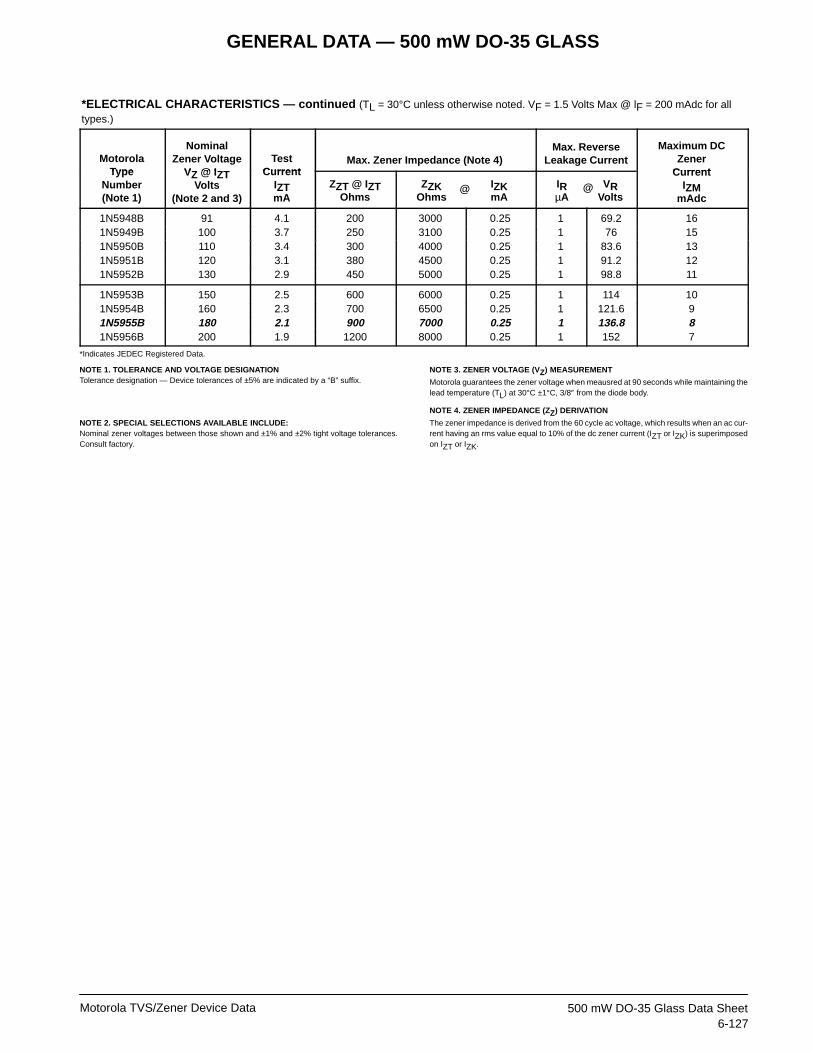
*ELECTRICAL CHARACTERISTICS — continued (TL = 30°C unless otherwise noted. VF = 1.5 Volts Max @ lF = 200 mAdc for alltypes.)
MotorolaType
NominalZener Voltage
VZ @ IZT
TestCurrent
Max. Zener Impedance (Note 4)Max. Reverse
Leakage CurrentMaximum DC
ZenerCurrentType
Number(Note 1)
VZ @ IZTVolts
(Note 2 and 3)
Curren tIZTmA
ZZT @ IZTOhms
ZZKOhms
IZKmA
@ IRµA
VRVolts
@Current
IZMmAdc
1N5948B 91 4.1 200 3000 0.25 1 69.2 161N5949B 100 3.7 250 3100 0.25 1 76 151N5950B 110 3.4 300 4000 0.25 1 83.6 131N5951B 120 3.1 380 4500 0.25 1 91.2 121N5952B 130 2.9 450 5000 0.25 1 98.8 11
1N5953B 150 2.5 600 6000 0.25 1 114 101N5954B 160 2.3 700 6500 0.25 1 121.6 91N5955B 180 2.1 900 7000 0.25 1 136.8 81N5956B 200 1.9 1200 8000 0.25 1 152 7
*Indicates JEDEC Registered Data.
NOTE 1. TOLERANCE AND VOLTAGE DESIGNATIONTolerance designation — Device tolerances of ±5% are indicated by a “B” suffix.
NOTE 2. SPECIAL SELECTIONS AVAILABLE INCLUDE:Nominal zener voltages between those shown and ±1% and ±2% tight voltage tolerances.Consult factory.
NOTE 3. ZENER VOLTAGE (VZ) MEASUREMENT
Motorola guarantees the zener voltage when meausred at 90 seconds while maintaining thelead temperature (TL) at 30°C ±1°C, 3/8″ from the diode body.
NOTE 4. ZENER IMPEDANCE (ZZ) DERIVATION
The zener impedance is derived from the 60 cycle ac voltage, which results when an ac cur-rent having an rms value equal to 10% of the dc zener current (IZT or IZK) is superimposedon IZT or IZK.

GENERAL DATA — 500 mW DO-35 GLASS
Motorola TVS/Zener Device Data6-128500 mW DO-35 Glass Data Sheet
ELECTRICAL CHARACTERISTICS (TA = 25°C unless otherwise noted) VF = 1.5 V Max, IF = 200 mA for all types)
Motorola
NominalZener Voltage
VZ @ IZT
TestCurrent
Max Zener Impedance(Note 3)
LeakageCurrent
MaximumZener
Current
SurgeCurrent
@ TA = 25°CMotoro laType No.(Note 1)
VZ @ IZTVolts
(Note 2)
Curren tIZTmA
ZZT @ IZTOhms
ZZK @ IZKOhms
IZKmA
IRµA Max
VRVolts
@Current
IZMmA
@ TA = 25°Cir – mA(Note 4)
3EZ3.9D5 3.9 192 4.5 400 1 80 1 630 4.43EZ4.3D5 4.3 174 4.5 400 1 30 1 590 4.13EZ4.7D5 4.7 160 4 500 1 20 1 550 3.83EZ5.1D5 5.1 147 3.5 550 1 5 1 520 3.5
3EZ5.6D5 5.6 134 2.5 600 1 5 2 480 3.33EZ6.2D5 6.2 121 1.5 700 1 5 3 435 3.13EZ6.8D5 6.8 110 2 700 1 5 4 393 2.93EZ7.5D5 7.5 100 2 700 0.5 5 5 360 2.66
3EZ8.2D5 8.2 91 2.3 700 0.5 5 6 330 2.443EZ9.1D5 9.1 82 2.5 700 0.5 3 7 297 2.23EZ10D5 10 75 3.5 700 0.25 3 7.6 270 23EZ11D5 11 68 4 700 0.25 1 8.4 245 1.82
3EZ12D5 12 63 4.5 700 0.25 1 9.1 225 1.663EZ13D5 13 58 4.5 700 0.25 0.5 9.9 208 1.543EZ14D5 14 53 5 700 0.25 0.5 10.6 193 1.433EZ15D5 15 50 5.5 700 0.25 0.5 11.4 180 1.33
3EZ16D5 16 47 5.5 700 0.25 0.5 12.2 169 1.253EZ17D5 17 44 6 750 0.25 0.5 13 159 1.183EZ18D5 18 42 6 750 0.25 0.5 13.7 150 1.113EZ19D5 19 40 7 750 0.25 0.5 14.4 142 1.05
3EZ20D5 20 37 7 750 0.25 0.5 15.2 135 13EZ22D5 22 34 8 750 0.25 0.5 16.7 123 0.913EZ24D5 24 31 9 750 0.25 0.5 18.2 112 0.833EZ27D5 27 28 10 750 0.25 0.5 20.6 100 0.74
3EZ28D5 28 27 12 750 0.25 0.5 21 96 0.713EZ30D5 30 25 16 1000 0.25 0.5 22.5 90 0.673EZ33D5 33 23 20 1000 0.25 0.5 25.1 82 0.613EZ36D5 36 21 22 1000 0.25 0.5 27.4 75 0.56
3EZ39D5 39 19 28 1000 0.25 0.5 29.7 69 0.513EZ43D5 43 17 33 1500 0.25 0.5 32.7 63 0.453EZ47D5 47 16 38 1500 0.25 0.5 35.6 57 0.423EZ51D5 51 15 45 1500 0.25 0.5 38.8 53 0.39
3EZ56D5 56 13 50 2000 0.25 0.5 42.6 48 0.363EZ62D5 62 12 55 2000 0.25 0.5 47.1 44 0.323EZ68D5 68 11 70 2000 0.25 0.5 51.7 40 0.293EZ75D5 75 10 85 2000 0.25 0.5 56 36 0.27
3EZ82D5 82 9.1 95 3000 0.25 0.5 62.2 33 0.243EZ91D5 91 8.2 115 3000 0.25 0.5 69.2 30 0.223EZ100D5 100 7.5 160 3000 0.25 0.5 76 27 0.23EZ110D5 110 6.8 225 4000 0.25 0.5 83.6 25 0.18
3EZ120D5 120 6.3 300 4500 0.25 0.5 91.2 22 0.163EZ130D5 130 5.8 375 5000 0.25 0.5 98.8 21 0.153EZ140D5 140 5.3 475 5000 0.25 0.5 106.4 19 0.143EZ150D5 150 5 550 6000 0.25 0.5 114 18 0.13
3EZ160D5 160 4.7 625 6500 0.25 0.5 121.6 17 0.123EZ170D5 170 4.4 650 7000 0.25 0.5 130.4 16 0.123EZ180D5 180 4.2 700 7000 0.25 0.5 136.8 15 0.113EZ190D5 190 4 800 8000 0.25 0.5 144.8 14 0.1
(continued)

GENERAL DATA — 500 mW DO-35 GLASS
Motorola TVS/Zener Device Data6-129
500 mW DO-35 Glass Data Sheet
ELECTRICAL CHARACTERISTICS — continued (TA = 25°C unless otherwise noted) VF = 1.5 V Max, IF = 200 mA for all types)
Motorola
NominalZener Voltage
VZ @ IZT
TestCurrent
Max Zener Impedance(Note 3)
LeakageCurrent
MaximumZener
Current
SurgeCurrent
@ TA = 25°CMotoro laType No.(Note 1)
VZ @ IZTVolts
(Note 2)
Curren tIZTmA
ZZT @ IZTOhms
ZZK @ IZKOhms
IZKmA
IRµA Max
VRVolts
@Current
IZMmA
@ TA = 25°Cir – mA(Note 4)
3EZ200D5 200 3.7 875 8000 0.25 0.5 152 13 0.13EZ220D5 220 3.4 1600 9000 0.25 1 167 12 0.093EZ240D5 240 3.1 1700 9000 0.25 1 182 11 0.093EZ270D5 270 2.8 1800 9000 0.25 1 205 10 0.08
3EZ300D5 300 2.5 1900 9000 0.25 1 228 9 0.073EZ330D5 330 2.3 2200 9000 0.25 1 251 8 0.063EZ360D5 360 2.1 2700 9000 0.25 1 274 8 0.063EZ400D5 400 1.9 3500 9000 0.25 1 304 7 0.06
NOTE 1. TOLERANCES
Suffix 5 indicates 5% tolerance. Any other tolerance will be considered as a special device.
NOTE 2. ZENER VOLTAGE (VZ) MEASUREMENTMotorola guarantees the zener voltage when measured at 40 ms ±10 ms 3/8″ from the diodebody, and an ambient temperature of 25°C (+8°C, –2°C)
NOTE 3. ZENER IMPEDANCE (ZZ) DERIVATION
The zener impedance is derived from the 60 cycle ac voltage, which results when an ac cur-rent having an rms value equal to 10% of the dc zener current (IZT or IZK) is superimposedon IZT or IZK.
NOTE 4. SURGE CURRENT (ir) NON-REPETITIVE
The rating listed in the electrical characteristics table is maximum peak, non-repetitive, re-verse surge current of 1/2 square wave or equivalent sine wave pulse of 1/120 second dura-tion superimposed on the test current, IZT, per JEDEC standards, however, actual device ca-pability is as described in Figure 3 of General Data sheet for Surmetic 30s.
NOTE 5. SPECIAL SELECTIONS AVAILABLE INCLUDE:Nominal zener voltages between those shown. Tight voltage tolerances such as ±1% and±2%. Consult factory.

GENERAL DATA — 500 mW DO-35 GLASS
Motorola TVS/Zener Device Data6-130500 mW DO-35 Glass Data Sheet
ELECTRICAL CHARACTERISTICS (TA = 25°C unless otherwise noted.) VF = 1.5 V Max, IF = 200 mA for all types.
Type No.
Zener Voltage(Note 2)
TestCurrent
IZT
Zener Impedance at I ZTf = 1000 Hz (Ohm)
Blocking VoltageTypical
TC
Surge Current@ TL = 25°C
ir – mAType No.(Note 1) Min Max
IZTmA Typ Max
Blocking VoltageIR = 1 µA
TC%/°C
ir – mA(Note 3)
MZD3.9 3.7 4.1 100 3.8 7 — –0.06 1380MZD4.3 4 4.6 100 3.8 7 — +0.055 1260MZD4.7 4.4 5 100 3.8 7 — +0.03 1190MZD5.1 4.8 5.4 100 2 5 — +0.03 1070MZD5.6 5.2 6 100 1 2 1.5 +0.038 970
MZD6.2 5.8 6.6 100 1 2 1.5 +0.045 890MZD6.8 6.4 7.2 100 1 2 2 +0.05 810MZD7.5 7 7.9 100 1 2 2 +0.058 730MZD8.2 7.7 8.7 100 1 2 3.5 +0.062 660MZD9.1 8.5 9.6 50 2 4 3.5 +0.068 605
MZD10 9.4 10.6 50 2 4 5 +0.075 550MZD11 10.4 11.6 50 4 7 5 +0.076 500MZD12 11.4 12.7 50 4 7 7 +0.077 454MZD13 12.4 14.1 50 5 10 7 +0.079 414MZD15 13.8 15.8 50 5 10 10 +0.082 380
MZD16 15.3 17.1 25 6 15 10 +0.083 344MZD18 16.8 19.1 25 6 15 10 +0.085 304MZD20 18.8 21.2 25 6 15 10 +0.086 285MZD22 20.8 23.3 25 6 15 12 +0.087 250MZD24 22.8 25.6 25 7 15 12 +0.088 225
MZD27 25.1 28.9 25 7 15 14 +0.09 205MZD30 28 32 25 8 15 14 +0.091 190MZD33 31 35 25 8 15 17 +0.092 170MZD36 34 38 10 21 40 17 +0.093 150MZD39 37 41 10 21 40 20 +0.094 135
MZD43 40 46 10 24 45 20 +0.095 125MZD47 44 50 10 24 45 24 +0.095 115MZD51 48 54 10 25 60 24 +0.096 110MZD56 52 60 10 25 60 28 +0.096 95MZD62 58 66 10 25 80 28 +0.097 90
MZD68 64 72 10 25 80 34 +0.097 80MZD75 70 79 10 30 100 34 +0.098 70MZD82 77 88 10 30 100 41 +0.098 65MZD91 85 96 5 60 200 41 +0.099 60MZD100 94 106 5 60 200 50 +0.11 55
MZD110 104 116 5 80 250 50 +0.11 50MZD120 114 127 5 80 250 60 +0.11 45MZD130 124 141 5 110 300 60 +0.11 —MZD150 138 156 5 110 300 75 +0.11 —MZD160 153 171 5 150 350 75 +0.11 —
MZD180 168 191 5 150 350 90 +0.11 —MZD200 188 212 5 150 350 90 +0.11 —
NOTE 1. TOLERANCE AND TYPE NUMBER DESIGNATIONThe type numbers listed have zener voltage min/max limits as shown.
NOTE 2. ZENER VOLTAGE (VZ) MEASUREMENTThe zener voltage is measured after the test current (IZT) has been applied for 40±10 millisec-onds, while maintaining a lead temperautre (TL) of 30°C at a point of 10 mm from the diodebody.
NOTE 3. (ir) NON-REPETITIVE SURGE CURRENT
Maximum peak, non-repetitive reverse surge current of half square wave or equivalent sinewave pulse of 50 ms duration, superimposed on the test current (IZT).
NOTE 4. SPECIAL SELECTIONS AVAILABLE INCLUDE:
Nominal zener voltages between those shown. Tight voltage tolerances such as ±1% and±2%. Consult factory.

GENERAL DATA — 500 mW DO-35 GLASS
Motorola TVS/Zener Device Data6-131
500 mW DO-35 Glass Data Sheet
ELECTRICAL CHARACTERISTICS (TA = 25°C unless otherwise noted) VF = 1.5 V Max, lF = 200 mA for all types
Motorola
NominalZener Voltage
VZ @ IZT Test Current
Max Zener Impedance(Note 3)
LeakageCurrent
SurgeCurrent
@ TA = 25°CMotoro laType No.(Note 1)
VZ @ IZTVolts
(Note 2)
Test Curren tIZTmA
ZZT @ IZTOhms
ZZK @ IZKOhms
IZKmA
IRµA Max
VRVolts
@
@ TA = 25°Cir – mA(Note 4)
MZP4728A 3.3 76 10 400 1 100 1 1380MZP4729A 3.6 69 10 400 1 100 1 1260MZP4730A 3.9 64 9 400 1 50 1 1190MZP4731A 4.3 58 9 400 1 10 1 1070MZP4732A 4.7 53 8 500 1 10 1 970
MZP4733A 5.1 49 7 550 1 10 1 890MZP4734A 5.6 45 5 600 1 10 2 810MZP4735A 6.2 41 2 700 1 10 3 730MZP4736A 6.8 37 3.5 700 1 10 4 660MZP4737A 7.5 34 4 700 0.5 10 5 605
MZP4738A 8.2 31 4.5 700 0.5 10 6 550MZP4739A 9.1 28 5 700 0.5 10 7 500MZP4740A 10 25 7 700 0.25 10 7.6 454MZP4741A 11 23 8 700 0.25 5 8.4 414MZP4742A 12 21 9 700 0.25 5 9.1 380
MZP4743A 13 19 10 700 0.25 5 9.9 344MZP4744A 15 17 14 700 0.25 5 11.4 304MZP4745A 16 15.5 16 700 0.25 5 12.2 285MZP4746A 18 14 20 750 0.25 5 13.7 250MZP4747A 20 12.5 22 750 0.25 5 15.2 225
MZP4748A 22 11.5 23 750 0.25 5 16.7 205MZP4749A 24 10.5 25 750 0.25 5 18.2 190MZP4750A 27 9.5 35 750 0.25 5 20.6 170MZP4751A 30 8.5 40 1000 0.25 5 22.8 150MZP4752A 33 7.5 45 1000 0.25 5 25.1 135
MZP4753A 36 7 50 1000 0.25 5 27.4 125MZP4754A 39 6.5 60 1000 0.25 5 29.7 115MZP4755A 43 6 70 1500 0.25 5 32.7 110MZP4756A 47 5.5 80 1500 0.25 5 35.8 95MZP4757A 51 5 95 1500 0.25 5 38.8 90
MZP4758A 56 4.5 110 2000 0.25 5 42.6 80MZP4759A 62 4 125 2000 0.25 5 47.1 70MZP4760A 68 3.7 150 2000 0.25 5 51.7 65MZP4761A 75 3.3 175 2000 0.25 5 56 60MZP4762A 82 3 200 3000 0.25 5 62.2 55
MZP4763A 91 2.8 250 3000 0.25 5 69.2 50MZP4764A 100 2.5 350 3000 0.25 5 76 451M110ZS5 110 2.3 450 4000 0.25 5 83.6 —1M120ZS5 120 2 550 4500 0.25 5 91.2 —1M130ZS5 130 1.9 700 5000 0.25 5 98.8 —
1M150ZS5 150 1.7 1000 6000 0.25 5 114 —1M160ZS5 160 1.6 1100 6500 0.25 5 121.6 —1M180ZS5 180 1.4 1200 7000 0.25 5 136.8 —1M200ZS5 200 1.2 1500 8000 0.25 5 152 —
The type numbers listed have a standard tolerance on the nominal zener voltage of ±5%. Thetolerance on the 1M type numbers is indicated by the digits following ZS in the part number.“5” indicates a ±5% VZ tolerance.
NOTE 1. TOLERANCE AND TYPE NUMBER DESIGNATION
NOTE 4. SURGE CURRENT (ir) NON-REPETITIVE
NOTE 2. ZENER VOLTAGE (VZ) MEASUREMENTMotorola guarantees the zener voltage when measured at 90 seconds while maintaining thelead temperature (TL) at 30°C ±1°C, 3/8″ from the diode body.
NOTE 3. ZENER IMPEDANCE (ZZ) DERIVATIONThe zener impedance is derived from the 60 cycle ac voltage, which results when an ac
The rating listed in the electrical characteristics table is maximum peak, non-repetitive,reverse surge current of 1/2 square wave or equivalent sine wave pulse of 1/120 secondduration superimposed on the test current, IZT, however, actual device capability is asdescribed in Figure 3 of General Data — Surmetic 30.
NOTE 5. SPECIAL SELECTIONS AVAILABLE INCLUDE:Nominal zener voltages between those shown. Tight voltage tolerances such as ±1% and±2%. Consult factory.
current having an rms value equal to 10% of the dc zener current (IZT or IZK) is superimposedon IZT or IZK.
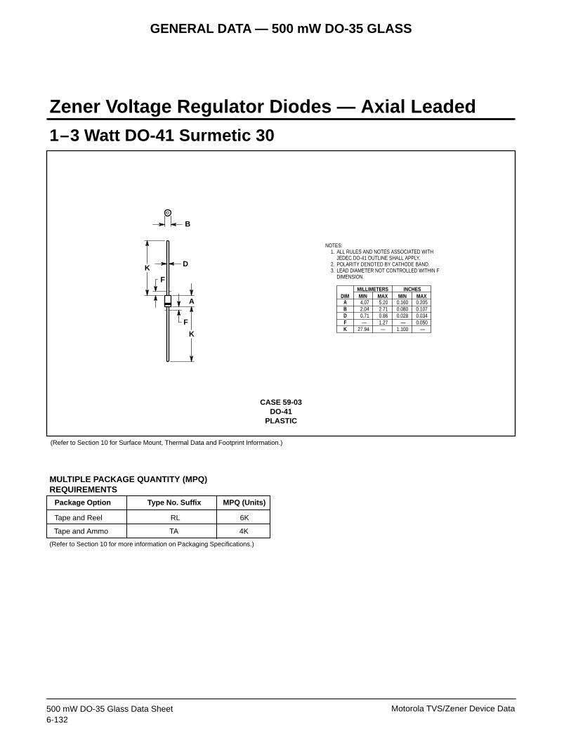
GENERAL DATA — 500 mW DO-35 GLASS
Motorola TVS/Zener Device Data6-132500 mW DO-35 Glass Data Sheet
1–3 Watt DO-41 Surmetic 30
MULTIPLE PACKAGE QUANTITY (MPQ)REQUIREMENTS
Zener Voltage Regulator Diodes — Axial Leaded
CASE 59-03DO-41
PLASTIC
(Refer to Section 10 for Surface Mount, Thermal Data and Footprint Information.)
(Refer to Section 10 for more information on Packaging Specifications.)
Package Option
Tape and Reel 6K
Type No. Suffix
RL
MPQ (Units)
Tape and Ammo TA 4K
NOTES:1. ALL RULES AND NOTES ASSOCIATED WITH
JEDEC DO-41 OUTLINE SHALL APPLY.2. POLARITY DENOTED BY CATHODE BAND.3. LEAD DIAMETER NOT CONTROLLED WITHIN F
DIMENSION.
K
K
F
A
F
D
MIN MINMAX MAXMILLIMETERS INCHES
DIM4.072.040.71—
27.94
5.202.710.861.27—
0.1600.0800.028
— 1.100
0.2050.1070.0340.050
—
ABDFK
B

MOTOROLASEMICONDUCTORTECHNICAL DATA
Motorola TVS/Zener Device Data6-1335 Watt Surmetic 40 Data Sheet
5 Watt Surmetic 40Silicon Zener Diodes
This is a complete series of 5 Watt Zener Diodes with tight limits and better operatingcharacteristics that reflect the superior capabilities of silicon-oxide-passivated junctions.All this is in an axial-lead, transfer-molded plastic package that offers protection in all com-mon environmental conditions.
Specification Features:• Up to 180 Watt Surge Rating @ 8.3 ms• Maximum Limits Guaranteed on Seven Electrical Parameters
Mechanical Characteristics:
CASE: Void-free, transfer-molded, thermosetting plasticFINISH: All external surfaces are corrosion resistant and leads are readily solderablePOLARITY: Cathode indicated by color band. When operated in zener mode, cathode
will be positive with respect to anodeMOUNTING POSITION: AnyWEIGHT: 0.7 gram (approx)WAFER FAB LOCATION: Phoenix, ArizonaASSEMBLY/TEST LOCATION: Seoul, Korea
MAXIMUM RATINGS
Rating Symbol Value Unit
DC Power Dissipation @ TL = 75°CLead Length = 3/8″Derate above 75°C
PD 5
40
Watts
mW/°C
Operating and Storage Junction Temperature Range TJ, Tstg – 65 to +200 °C
Figure 1. Power Temperature Derating Curve
TL, LEAD TEMPERATURE (°C)
PD
, MAX
IMU
M P
OW
ER D
ISSI
PATI
ON
(WAT
TS) 8
6
4
2
00 20 40 60 80 100 120 140 160 180 200
L = LEAD LENGTHL = TO HEAT SINKL = (SEE FIGURE 5)L = 1/8″
L = 3/8″
L = 1″
1N5333Bthrough1N5388B
CASE 17PLASTIC
5 WATTZENER REGULATOR
DIODES3.3–200 VOLTS

1N5333B through 1N5388B
Motorola TVS/Zener Device Data6-1345 Watt Surmetic 40 Data Sheet
Devices listed in bold, italic are Motorola preferred devices.
ELECTRICAL CHARACTERISTICS (TA = 25°C unless otherwise noted, VF = 1.2 Max @ IF = 1 A for all types)
JEDEC
NominalZener
Voltage TestMax Zener Impedance
Max ReverseLeakage Current Max
Surge Max Voltage
MaximumRegulatorCurrent
JEDECType No.(Note 1)
VoltageVZ @ IZT
Volts(Note 2)
TestCurrent
IZTmA
ZZT @IZTOhms
(Note 2)
ZZK @ IZK = 1 mAOhms
(Note 2)IRµA
VRVolts
@
SurgeCurrentir, Amps(Note 3)
Max VoltageRegulation∆VZ, Volt(Note 4)
Curren tIZMmA
(Note 5)
1N5333B 3.3 380 3 400 300 1 20 0.85 14401N5334B 3.6 350 2.5 500 150 1 18.7 0.8 13201N5335B 3.9 320 2 500 50 1 17.6 0.54 12201N5336B 4.3 290 2 500 10 1 16.4 0.49 11001N5337B 4.7 260 2 450 5 1 15.3 0.44 1010
1N5338B 5.1 240 1.5 400 1 1 14.4 0.39 9301N5339B 5.6 220 1 400 1 2 13.4 0.25 8651N5340B 6 200 1 300 1 3 12.7 0.19 7901N5341B 6.2 200 1 200 1 3 12.4 0.1 7651N5342B 6.8 175 1 200 10 5.2 11.5 0.15 700
1N5343B 7.5 175 1.5 200 10 5.7 10.7 0.15 6301N5344B 8.2 150 1.5 200 10 6.2 10 0.2 5801N5345B 8.7 150 2 200 10 6.6 9.5 0.2 5451N5346B 9.1 150 2 150 7.5 6.9 9.2 0.22 5201N5347B 10 125 2 125 5 7.6 8.6 0.22 475
1N5348B 11 125 2.5 125 5 8.4 8 0.25 4301N5349B 12 100 2.5 125 2 9.1 7.5 0.25 3951N5350B 13 100 2.5 100 1 9.9 7 0.25 3651N5351B 14 100 2.5 75 1 10.6 6.7 0.25 3401N5352B 15 75 2.5 75 1 11.5 6.3 0.25 315
1N5353B 16 75 2.5 75 1 12.2 6 0.3 2951N5354B 17 70 2.5 75 0.5 12.9 5.8 0.35 2801N5355B 18 65 2.5 75 0.5 13.7 5.5 0.4 2651N5356B 19 65 3 75 0.5 14.4 5.3 0.4 2501N5357B 20 65 3 75 0.5 15.2 5.1 0.4 237
1N5358B 22 50 3.5 75 0.5 16.7 4.7 0.45 2161N5359B 24 50 3.5 100 0.5 18.2 4.4 0.55 1981N5360B 25 50 4 110 0.5 19 4.3 0.55 1901N5361B 27 50 5 120 0.5 20.6 4.1 0.6 1761N5362B 28 50 6 130 0.5 21.2 3.9 0.6 170
1N5363B 30 40 8 140 0.5 22.8 3.7 0.6 1581N5364B 33 40 10 150 0.5 25.1 3.5 0.6 1441N5365B 36 30 11 160 0.5 27.4 3.3 0.65 1321N5366B 39 30 14 170 0.5 29.7 3.1 0.65 1221N5367B 43 30 20 190 0.5 32.7 2.8 0.7 110
1N5368B 47 25 25 210 0.5 35.8 2.7 0.8 1001N5369B 51 25 27 230 0.5 38.8 2.5 0.9 931N5370B 56 20 35 280 0.5 42.6 2.3 1 861N5371B 60 20 40 350 0.5 42.5 2.2 1.2 791N5372B 62 20 42 400 0.5 47.1 2.1 1.35 76
1N5373B 68 20 44 500 0.5 51.7 2 1.5 701N5374B 75 20 45 620 0.5 56 1.9 1.6 631N5375B 82 15 65 720 0.5 62.2 1.8 1.8 581N5376B 87 15 75 760 0.5 66 1.7 2 54.51N5377B 91 15 75 760 0.5 69.2 1.6 2.2 52.5
1N5378B 100 12 90 800 0.5 76 1.5 2.5 47.51N5379B 110 12 125 1000 0.5 83.6 1.4 2.5 431N5380B 120 10 170 1150 0.5 91.2 1.3 2.5 39.51N5381B 130 10 190 1250 0.5 98.8 1.2 2.5 36.61N5382B 140 8 230 1500 0.5 106 1.2 2.5 34
(continued)
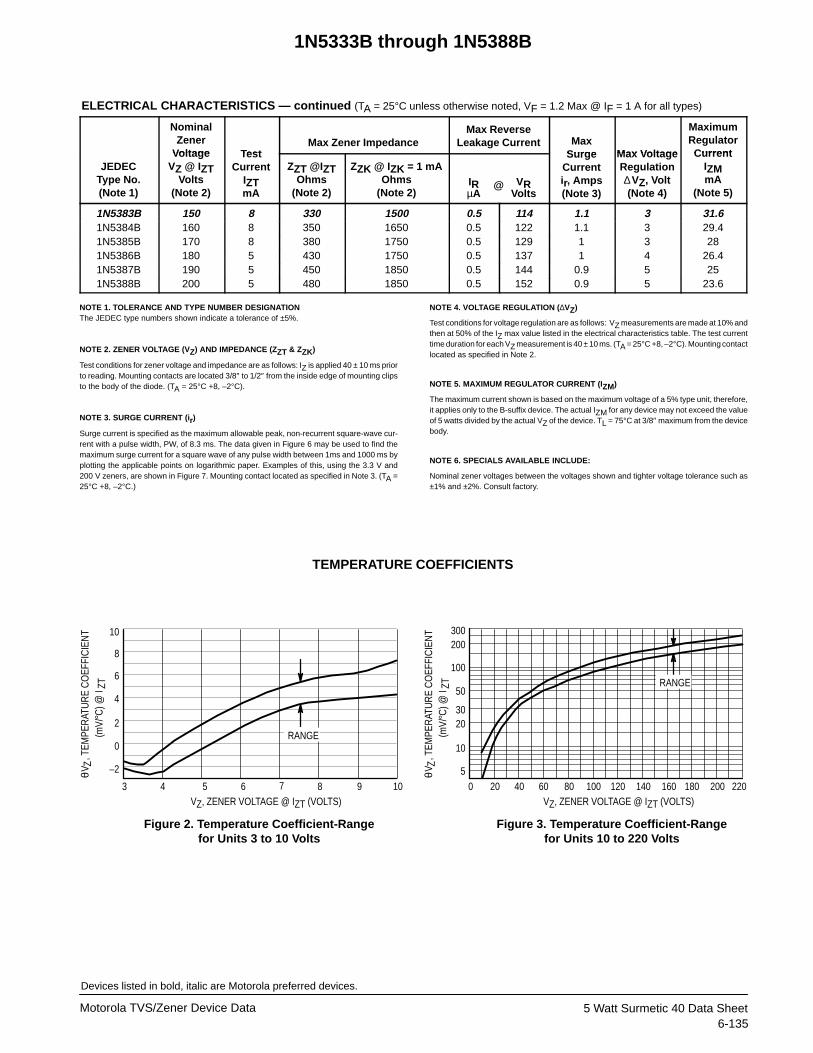
1N5333B through 1N5388B
Motorola TVS/Zener Device Data6-135
5 Watt Surmetic 40 Data Sheet
Devices listed in bold, italic are Motorola preferred devices.
ELECTRICAL CHARACTERISTICS — continued (TA = 25°C unless otherwise noted, VF = 1.2 Max @ IF = 1 A for all types)
JEDEC
NominalZener
Voltage TestMax Zener Impedance
Max ReverseLeakage Current Max
Surge Max Voltage
MaximumRegulatorCurrent
JEDECType No.(Note 1)
VoltageVZ @ IZT
Volts(Note 2)
TestCurrent
IZTmA
ZZT @IZTOhms
(Note 2)
ZZK @ IZK = 1 mAOhms
(Note 2)IRµA
VRVolts
@
SurgeCurrentir, Amps(Note 3)
Max VoltageRegulation∆VZ, Volt(Note 4)
Curren tIZMmA
(Note 5)
1N5383B 150 8 330 1500 0.5 114 1.1 3 31.61N5384B 160 8 350 1650 0.5 122 1.1 3 29.41N5385B 170 8 380 1750 0.5 129 1 3 281N5386B 180 5 430 1750 0.5 137 1 4 26.41N5387B 190 5 450 1850 0.5 144 0.9 5 251N5388B 200 5 480 1850 0.5 152 0.9 5 23.6
NOTE 1. TOLERANCE AND TYPE NUMBER DESIGNATIONThe JEDEC type numbers shown indicate a tolerance of ±5%.
NOTE 2. ZENER VOLTAGE (VZ) AND IMPEDANCE (ZZT & ZZK)
Test conditions for zener voltage and impedance are as follows: IZ is applied 40 ± 10 ms priorto reading. Mounting contacts are located 3/8″ to 1/2″ from the inside edge of mounting clipsto the body of the diode. (TA = 25°C +8, –2°C).
NOTE 3. SURGE CURRENT (ir)
Surge current is specified as the maximum allowable peak, non-recurrent square-wave cur-rent with a pulse width, PW, of 8.3 ms. The data given in Figure 6 may be used to find themaximum surge current for a square wave of any pulse width between 1ms and 1000 ms byplotting the applicable points on logarithmic paper. Examples of this, using the 3.3 V and200 V zeners, are shown in Figure 7. Mounting contact located as specified in Note 3. (TA =25°C +8, –2°C.)
NOTE 4. VOLTAGE REGULATION ( ∆VZ)
Test conditions for voltage regulation are as follows: VZ measurements are made at 10% andthen at 50% of the IZ max value listed in the electrical characteristics table. The test currenttime duration for each VZ measurement is 40 ± 10 ms. (TA = 25°C +8, –2°C). Mounting contactlocated as specified in Note 2.
NOTE 5. MAXIMUM REGULATOR CURRENT (I ZM)
The maximum current shown is based on the maximum voltage of a 5% type unit, therefore,it applies only to the B-suffix device. The actual IZM for any device may not exceed the valueof 5 watts divided by the actual VZ of the device. TL = 75°C at 3/8″ maximum from the devicebody.
NOTE 6. SPECIALS AVAILABLE INCLUDE:
Nominal zener voltages between the voltages shown and tighter voltage tolerance such as±1% and ±2%. Consult factory.
TEMPERATURE COEFFICIENTS
Figure 2. Temperature Coefficient-Rangefor Units 3 to 10 Volts
Figure 3. Temperature Coefficient-Rangefor Units 10 to 220 Volts
VZ, ZENER VOLTAGE @ IZT (VOLTS)
10
8
6
4
2
0
–2
3 4 5 6 7 8 9 10
RANGE
300200
100
50
3020
10
50 20 40 60 80 100 120 140 160 180 200 220
VZ, ZENER VOLTAGE @ IZT (VOLTS)
θVZ
, TEM
PER
ATU
RE
CO
EFFI
CIE
NT
(mV/
°C) @
IZT
θVZ
, TEM
PER
ATU
RE
CO
EFFI
CIE
NT
(mV/
°C) @
IZT RANGE

1N5333B through 1N5388B
Motorola TVS/Zener Device Data6-1365 Watt Surmetic 40 Data Sheet
Devices listed in bold, italic are Motorola preferred devices.
Figure 4. Typical Thermal ResponseL, Lead Length = 3/8 Inch
Figure 5. Typical Thermal Resistance Figure 6. Maximum Non-Repetitive Surge Currentversus Nominal Zener Voltage
(See Note 3)
θ JL
(t, D
), TR
ANSI
ENT
THER
MAL
RES
ISTA
NC
EJU
NC
TIO
N-T
O-L
EAD
( °C
/W)
20
10
5
2
1
0.5
0.20.00
10.00
50.01 0.05 0.1 0.5 1 5 10 20 50 100
D = 0.5
D = 0.2
D = 0.1
D = 0.05
D = 0.01
D = 0
NOTE: BELOW 0.1 SECOND, THERMALNOTE: RESPONSE CURVE IS APPLICABLENOTE: TO ANY LEAD LENGTH (L).
DUTY CYCLE, D = t1/t2SINGLE PULSE ∆ TJL = θJL(t)PPK
REPETITIVE PULSES ∆ TJL = θJL(t, D)PPK
PPK t1
t2
t, TIME (SECONDS)
40
30
20
10
00 0.2 0.4 0.6 0.8 1
PRIMARY PATH OFCONDUCTION IS THROUGH
THE CATHODE LEAD
L L
L, LEAD LENGTH TO HEAT SINK (INCH)JL, J
UN
CTI
ON
-TO
-LEA
D T
HER
MAL
RES
ISTA
NC
E (
θ°C
/W)
i r, P
EAK
SUR
GE
CU
RR
ENT
(AM
PS)
40
20
10
4
2
1
0.1
0.2
0.4
3 4 6 8 10 20 30 40 60 80 100 200
*SQUARE WAVE PW = 100 ms*
PW = 1000 ms*
PW = 1 ms*
PW = 8.3 ms*
NOMINAL VZ (V)
3020
10
0.1
0.2
0.5
1
2
5
1 10 100 1000
1000
100
10
1
0.11 2 3 4 5 6 7 8 9 10
I Z, Z
ENER
CU
RR
ENT
(mA)
PW, PULSE WIDTH (ms) VZ, ZENER VOLTAGE (VOLTS)
Figure 7. Peak Surge Current versus Pulse Width(See Note 3)
Figure 8. Zener Voltage versus Zener CurrentVZ = 3.3 thru 10 Volts
VZ = 200 V
VZ = 3.3 V
PLOTTED FROM INFORMATIONGIVEN IN FIGURE 6
TC = 25°C
T = 25°C
i r, P
EAK
SUR
GE
CU
RR
ENT
(AM
PS)
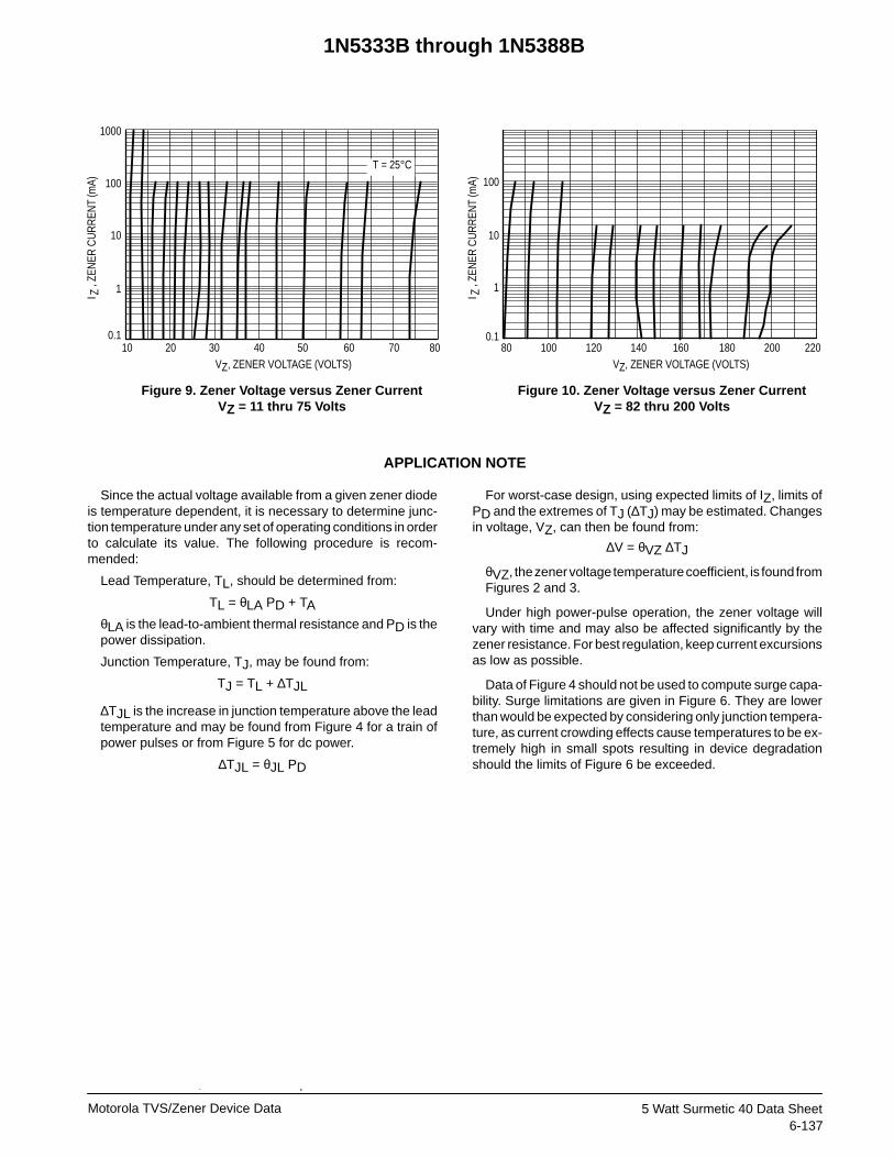
1N5333B through 1N5388B
Motorola TVS/Zener Device Data6-137
5 Watt Surmetic 40 Data Sheet
Devices listed in bold, italic are Motorola preferred devices.
I Z, Z
ENER
CU
RR
ENT
(mA)
VZ, ZENER VOLTAGE (VOLTS)
1000
100
10
1
0.110 20 30 40 50 60 70 80
100
10
1
0.180 100 120 140 160 180 200 220
VZ, ZENER VOLTAGE (VOLTS)
I Z, Z
ENER
CU
RR
ENT
(mA)
T = 25°C
Figure 9. Zener Voltage versus Zener CurrentVZ = 11 thru 75 Volts
Figure 10. Zener Voltage versus Zener CurrentVZ = 82 thru 200 Volts
APPLICATION NOTE
Since the actual voltage available from a given zener diodeis temperature dependent, it is necessary to determine junc-tion temperature under any set of operating conditions in orderto calculate its value. The following procedure is recom-mended:
Lead Temperature, TL, should be determined from:
TL = θLA PD + TAθLA is the lead-to-ambient thermal resistance and PD is thepower dissipation.
Junction Temperature, TJ, may be found from:
TJ = TL + ∆TJL
∆TJL is the increase in junction temperature above the leadtemperature and may be found from Figure 4 for a train ofpower pulses or from Figure 5 for dc power.
∆TJL = θJL PD
For worst-case design, using expected limits of IZ, limits ofPD and the extremes of TJ (∆TJ) may be estimated. Changesin voltage, VZ, can then be found from:
∆V = θVZ ∆TJ
θVZ, the zener voltage temperature coefficient, is found fromFigures 2 and 3.
Under high power-pulse operation, the zener voltage willvary with time and may also be affected significantly by thezener resistance. For best regulation, keep current excursionsas low as possible.
Data of Figure 4 should not be used to compute surge capa-bility. Surge limitations are given in Figure 6. They are lowerthan would be expected by considering only junction tempera-ture, as current crowding effects cause temperatures to be ex-tremely high in small spots resulting in device degradationshould the limits of Figure 6 be exceeded.

Motorola TVS/Zener Device Data6-138
5 Watt Surmetic 40 Data Sheet
5 Watt Surmetic 40
MULTIPLE PACKAGE QUANTITY (MPQ)REQUIREMENTS
Zener Voltage Regulator Diodes — Axial Leaded
CASE 17-02PLASTIC
(Refer to Section 10 for Surface Mount, Thermal Data and Footprint Information.)
(Refer to Section 10 for more information on Packaging Specifications.)
Package Option
Tape and Reel 4K
Type No. Suffix
RL
MPQ (Units)
Tape and Ammo TA 2K
B
A
K
D
FK
F1
2
NOTE:1. LEAD DIAMETER & FINISH NOT CONTROLLED
WITHIN DIM F.
MIN MINMAX MAXINCHES MILLIMETERS
DIM8.383.300.94—
25.40
8.893.681.091.27
31.75
0.3300.1300.037
— 1.000
0.3500.1450.0430.0501.250
ABDFK
Related Documents